ICGOO在线商城 > PTH03000WAD

 Datasheet下载
- 型号: PTH03000WAD
- 制造商: Texas Instruments
- 库位|库存: xxxx|xxxx
- 要求:
| 数量阶梯 | 香港交货 | 国内含税 |
| +xxxx | $xxxx | ¥xxxx |
查看当月历史价格
查看今年历史价格
PTH03000WAD产品简介:
ICGOO电子元器件商城为您提供PTH03000WAD由Texas Instruments设计生产,在icgoo商城现货销售,并且可以通过原厂、代理商等渠道进行代购。 提供PTH03000WAD价格参考以及Texas InstrumentsPTH03000WAD封装/规格参数等产品信息。 你可以下载PTH03000WAD参考资料、Datasheet数据手册功能说明书, 资料中有PTH03000WAD详细功能的应用电路图电压和使用方法及教程。
| 参数 | 数值 |
| 产品目录 | |
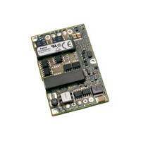
| 描述 | MODULE PIP 3.3VIN 6A ADJ T/H非隔离式DC/DC转换器 6A 3.3V-In Wide-Out Adj Plug-in Pwr Mdl |
| 产品分类 | DC DC ConvertersDC/DC转换器 |
| 品牌 | Texas Instruments |
| 产品手册 | |
| 产品图片 |
|
| rohs | 符合RoHS无铅 / 符合限制有害物质指令(RoHS)规范要求 |
| 产品系列 | 非隔离式DC/DC转换器,Texas Instruments PTH03000WADPTH03000W |
| 数据手册 | |
| 产品型号 | PTH03000WAD |
| 产品 | Non-Isolated / POL |
| 产品种类 | 非隔离式DC/DC转换器 |
| 其它名称 | 296-32711 |
| 制造商产品页 | http://www.ti.com/general/docs/suppproductinfo.tsp?distId=10&orderablePartNumber=PTH03000WAD |
| 功率(W)-制造系列 | 15W |
| 功率(W)-最大值 | 15W |
| 包装 | 托盘 |
| 商标 | Texas Instruments |
| 大小/尺寸 | 0.75" 长 x 0.50" 宽 x 0.34" 高(19.1mm x 12.7mm x 8.6mm) |
| 安装类型 | 通孔 |
| 安装风格 | Through Hole |
| 封装 | Tray |
| 封装/外壳 | 5-DIP 模块 |
| 封装/箱体尺寸 | Through Hole Module |
| 工作温度 | -40°C ~ 85°C |
| 工作温度范围 | - 40 C to + 85 C |
| 工厂包装数量 | 56 |
| 效率 | 93% |
| 标准包装 | 56 |
| 特性 | - |
| 电压-输入(最大值) | 3.6V |
| 电压-输入(最小值) | 3V |
| 电压-输出1 | 0.9 ~ 2.5 V |
| 电压-输出2 | - |
| 电压-输出3 | - |
| 电压-隔离 | - |
| 电流-输出(最大值) | 6A |
| 类型 | 非隔离 PoL 模块 |
| 系列 | PTH03000W |
| 输入电压—公称值 | 3.3 V |
| 输入电压范围 | 3 V to 3.6 V |
| 输出功率 | 115 W |
| 输出数 | 1 |
| 输出电压—通道1 | 0.9 V to 2.5 V |
| 输出电流—通道1 | 6 A |
| 输出端数量 | 1 |


PDF Datasheet 数据手册内容提取
PTH03000W —3.3-V Input 6-A, 3.3-V Input Non-Isolated Wide-Output Adjust Power Module SLTS200C – MAY 2003 – REVISED DECEMBER 2003 Features • Up to 6-A Output Current • Output Current Limit • 3.3 V Input Voltage • Over-Temperature Protection • Wide-Output Voltage Adjust • Operating Temp: –40 to +85 °C (0.9 V to 2.5 V) • Surface Mount Package • Efficiencies up to 95 % • Safety Agency Approvals (Pending): • 115 W/in³ Power Density UL 1950, CSA 22.2 950, EN60950 NOMINAL SIZE = 0.75 in x 0.5 in • On/Off Inhibit & VDE (19,05 mm x 12,7 mm) • Under-Voltage Lockout Description Pin Configuration The PTH03000 series of non-isolated Operating features include an on/off Pin Function power modules are small in size and high inhibit, output voltage adjust (trim), an 1 GND on performance. Using double-sided sur- output current limit, and over-temperature 2 Vin face mount construction and synchronous protection. 3 Inhibit * rectification technology, these regulators Target applications include telecom, 4 Vo Adjust deliver up to 6 A of output current while industrial, and general purpose circuits, 5 Vout occupying a PCB area of about half the including low-power dual-voltage systems * Denotes negative logic: size of a standard postage stamp. They that use a DSP, microprocessor, or ASIC. Open = Output On Ground = Output Off are an ideal choice for applications where Package options include both through- space, performance and cost are impor- hole and surface mount configurations. tant design constraints. The series operates from an input voltage of 3.3 V to provide step-down power conversion to any output voltage over the range, 0.9 V to 2.5 V. The out- put voltage of the PTH03000W is set within this range using a single resistor. Standard Application Rset =Required to set the output voltage to a value higher than 0.9 V (see spec. table for values) Cin =Required 100 µF capacitor Cout=Optional 100 µF capacitor VOUT 1 5 V PTH03000W IN 2 (Top View) 3 4 C C OUT IN 100 µF 1(R0e0q µuFired) R1 S%ET, 0.1 W E(Olepctitoronlaylt)ic (Required) Inhibit GND GND For technical support and further information visit http://power.ti.com
PTH03000W —3.3-V Input 6-A, 3.3-V Input Non-Isolated Wide-Output Adjust Power Module SLTS200C – MAY 2003 – REVISED DECEMBER 2003 Ordering Information Output Voltage (PTH03000(cid:1)xx) Package Options (PTH03000x(cid:1)(cid:1))(1) Code Voltage Code Description Pkg Ref. (2) W 0.9 V – 2.5 V (Adjust) AH Horiz. T/H (EUS) AS SMD, Standard (3) (EUT) Notes: (1) Add “T” to end of part number for tape and reel on SMD packages only. (2) Reference the applicable package reference drawing for the dimensions and PC board layout (3) “Standard” option specifies 63/37, Sn/Pb pin solder material. Pin Descriptions Vin: The positive input voltage power node to the mod- Vo Adjust: A 0.1 W 1 % resistor must be directly connected ule, which is referenced to common GND. between this pin and the GND pin to set the output voltage Vout: The regulated positive power output with respect to a value higher than 0.9 V. The temperature stability to the GND node. of the resistor should be 100 ppm/°C (or better). The set point range for the output voltage is from 0.9 V to 2.5 V. GND: This is the common ground connection for the The resistor required for a given output voltage may be ‘Vin’ and ‘Vout’ power connections. It is also the 0 VDC calculated from the following formula. If left open circuit, reference for the ‘Inhibit’ and ‘Vo Adjust’ control inputs. the output voltage will default to its lowest value. For Inhibit: The Inhibit pin is an open-collector/drain negative further information on output voltage adjustment, consult logic input that is referenced to GND. Applying a low- the related application note. level ground signal to this input disables the module’s output and turns off the output voltage. When the Inhibit control is active, the input current drawn by the regulator Rset = 10 kΩ · 0.891 V – 4.99 kΩ is significantly reduced. If the Inhibit pin is left open- Vout – 0.9 V circuit, the module will produce an output whenever a The specification table gives the preferred resistor values valid input source is applied. for a number of standard output voltages. For technical support and further information visit http://power.ti.com
PTH03000W —3.3-V Input 6-A, 3.3-V Input Non-Isolated Wide-Output Adjust Power Module SLTS200C– MAY 2003 – REVISED DECEMBER 2003 Environmental & Absolute Maximum Ratings Characteristics Symbols Conditions Min Typ Max Units Operating Temperature Range Ta Over Vin Range –40 (i) — +85 °C Solder Reflow Temperature Treflow Surface temperature of module body or pins 235 (ii) °C Storage Temperature Ts — –40 — +125 °C Over Temperature Protection OTP IC junction temperature — 150 — °C Mechanical Shock Per Mil-STD-883D, Method 2002.3 — 500 — G’s 1 msec, ½ sine, mounted Mechanical Vibration Mil-STD-883D, Method 2007.2 — 20 — G’s 20-2000 Hz Weight — — 2 — grams Flammability — Meets UL 94V-O Notes: (i) During reflow of SMD package version do not elevate peak temperature of the module, pins or internal components above the stated maximum. Electrical Specifications Unless otherwise stated, Ta =25 °C, Vin =3.3 V, Vo =2 V, Cin =100 µF, Cout =0 µF, and Io =Iomax PTH03000W Characteristics Symbols Conditions Min Typ Max Units Output Current Io 0.9 V ≤ Vo ≤ 2.5 V, Ta =60 °C, 200 LFM airflow 0 — 6 (1) A Ta =25 °C, natural convection 0 — 6 (1) Input Voltage Range Vin Over Io range 3 — 3.6 V Set-Point Voltage Tolerance Vo tol — — ±2 (2) %Vo Temperature Variation ∆Regtemp –40 °C <Ta < +85 °C — ±0.5 — %Vo Line Regulation ∆Regline Over Vin range — ±5 — mV Load Regulation ∆Regload Over Io range — ±5 — mV Total Output Variation ∆Regtot I–n4c0l u°dCe s≤ sTeta- ≤p o+i8n5t, °lCine, load, — — ±3 (2) %Vo Efficiency η Io =4 A RRRRRRSSSSSSEEEEEETTTTTT ====== 5349287...420876..97635 Ω kkkkkΩΩΩΩΩ VVVVVVoooooo ====== 221111......508520 VVVVVV —————— 999888310864 —————— % Vo Ripple (pk-pk) Vr 20 MHz bandwidth — 20 — mVpp Transient Response 1 A/µs load step, 50 to 100 % Iomax, Vo =1.8 V, Cout =100 µF t∆trVtr RVeo coovveerr/yu ntidmeershoot —— 17000 —— mµSVec Current Limit Ilim ∆Vo = –50 mV — 13 — A Under-Voltage Lockout UVLO Vin increasing — 2.95 3 V Vin decreasing 2.6 2.8 — Inhibit Control (pin 3) Referenced to GND Input High Voltage VIH Vin –0.5 — Open (3) V Input Low Voltage VIL –0.2 — 0.8 Input Low Current IIL Pin 3 to GND — –10 — µA Standby Input Current Iin inh pins 1 & 3 connected — 1 — mA Switching Frequency ƒs Over Vin and Io ranges — 700 — kHz External Input Capacitance Cin 100 (4) — — µF External Output Capacitance Cout Capacitance value non-ceramic 0 100 (5) 1,000 (6) µF ceramic 0 — 300 Equiv. series resistance (non-ceramic) 4 (7) — — mΩ Reliability MTBF Per Bellcore TR-332 28 — — 106 Hrs 50 % stress, Ta =40 °C, ground benign Notes:(1) See SOA curves or consult factory for appropriate derating. (2) The set-point voltage tolerance is affected by the tolerance and stability ofRSET. The stated limit is unconditionally met if RSET has a tolerance of 1 % with 100 ppm/°C or better temperature stability. (3) The Inhibit control (pin 3) has an internal pull-up to Vin, and if left open-circuit the module will operate when input power is applied. A small low- leakage (<100 nA) MOSFET is recommended to control this input. See application notes for more information. (4) The regulator requires a minimum of 100 µF input capacitor with a minimum 300 mArms ripple current rating. For further information, consult the related application note on Capacitor Recommendations. (5) An external output capacitor is not required for basic operation. Adding 100 µF of distributed capacitance at the load will improve the transient response. (6) This is the calculated maximum. The minimum ESR limitation will often result in a lower value. Consult the application notes for further guidance. (7) This is the typical ESR for all the electrolytic (non-ceramic) output capacitance. Use 7 mΩ as the minimum when using max-ESR values to calculate. For technical support and further information visit http://power.ti.com
PTH03000W —3.3-V Input Typical Characteristics 6-A, 3.3-V Input Non-Isolated Wide-Output Adjust Power Module SLTS200C – MAY 2003 – REVISED DECEMBER 2003 Characteristic Data; Vin =3.3V (See Note A) Safe Operating Area; Vin =3.3 V (See Note B) Efficiency vs Output Current All Output Voltages 100 90 80 90 VOUT C) Efficiency - % 7800 221111......508520 VV VVVV bient Temperature (°45670000 A1Nir0af0lto LCwFoMnv m 60 A 30 50 20 0 1 2 3 4 5 6 0 1 2 3 4 5 6 Iout - Amps Iout (A) Ripple vs Output Current 50 40 VOUT 1.0 V mV30 1.2 V ple - 11..58 VV Rip20 2.0 V 2.5 V 10 0 0 1 2 3 4 5 6 Iout (A) Power Dissipation vs Output Current 2 1.6 Watts1.2 Pd - 0.8 0.4 0 0 1 2 3 4 5 6 Iout (A) Note A: Characteristic data has been developed from actual products tested at 25°C. This data is considered typical data for the Converter. Note B: SOA curves represent the conditions at which internal components are at or below the manufacturer’s maximum operating temperatures. Derating limits apply to modules soldered directly to a 4 in. × 4 in. double-sided PCB with 1 oz. copper. For technical support and further information visit http://power.ti.com
Application Notes PTH03000W Capacitor Recommendations for the PTH03000W, Wide-Output Adjust Power Modules Input Capacitor T510 capacitor series are suggested over many other The recommended input capacitor(s) is determined by tantalum types due to their higher rated surge, power the 100 µF minimum capacitance and 300 mArms mini- dissipation, and ripple current capability. As a caution mum ripple current rating. many general purpose tantalum capacitors have consid- Ripple current, less than 300 mΩ equivalent series resis- erably higher ESR, reduced power dissipation and lower ripple current capability. These capacitors are also less tance (ESR), and temperature are the major considerations reliable as they have lower power dissipation and surge when selecting input capacitors. Unlike polymer tantalum, current ratings. Tantalum capacitors that do not have a regular tantalum capacitors have a recommended mini- mum voltage rating of 2 × (maximum DC voltage + AC stated ESR or surge current rating are not recommended for power applications. ripple). This is standard practice to ensure reliability. When specifying Os-Con and polymer tantalum capacitors For improved ripple reduction on the input bus, ceramic for the output, the minimum ESR limit will be encoun- capacitors [2] may used to complement electrolytic types tered well before the maximum capacitance value is and achieve the minimum required capacitance. reached. Output Capacitors (Optional) Capacitor Table For applications with load transients (sudden changes in Table 1-1 identifies the characteristics of capacitors from a load current), regulator response will benefit from an number of vendors with acceptable ESR and ripple current external output capacitance. The recommended output (rms) ratings. The recommended number of capacitors capacitance of 100 µF will allow the module to meet required at both the input and output buses is identified its transient response specification (see product data sheet). for each capacitor type. For most applications, a high quality computer-grade aluminum electrolytic capacitor is adequate. These capaci- This is not an extensive capacitor list. Capacitors from other tors provide decoupling over the frequency range, 2 kHz vendors are available with comparable specifications. Those to 150 kHz, and are suitable for ambient temperatures listed are for guidance. The RMS ripple current rating and above 0 °C. For operation below 0 °C tantalum, ceramic ESR (at 100 kHz) are critical parameters necessary to insure or Os-Con type capacitors are recommended. When using both optimum regulator performance and long capacitor life. one or more non-ceramic capacitors, the calculated equiva- lent ESR should be no lower than 4 mΩ (7 mΩ using the Designing for Very Fast Load Transients manufacturer’s maximum ESR for a single capacitor). A The transient response of the DC/DC converter has been list of preferred low-ESR type capacitors are identified characterized using a load transient with a di/dt of 1 A/µs. in Table 1-1. The typical voltage deviation for this load transient is given in the data sheet specification table using the Ceramic Capacitors optional value of output capacitance. As the di/dt of a Above 150 kHz the performance of aluminum electrolytic transient is increased, the response of a converter’s regu- capacitors becomes less effective. To further improve the lation circuit ultimately depends on its output capacitor reflected input ripple current [2] or the output transient decoupling network. This is an inherent limitation with response, multilayer ceramic capacitors can also be added. any DC/DC converter once the speed of the transient Ceramic capacitors have very low ESR and their resonant exceeds its bandwidth capability. If the target application frequency is higher than the bandwidth of the regulator. specifies a higher di/dt or lower voltage deviation, the When used on the output their combined ESR is not requirement can only be met with additional output critical as long as the total value of ceramic capacitance capacitor decoupling. In these cases special attention does not exceed 300 µF. Also, to prevent the formation of must be paid to the type, value and ESR of the capacitors local resonances, do not place more than five identical ce- selected. ramic capacitors in parallel with values of 10 µF or greater. If the transient performance requirements exceed that Tantalum Capacitors specified in the data sheet, the selection of output ca- pacitors becomes more important. For further guidance Tantalum type capacitors can be used at both the input consult the separate application note, “Selecting Output and output, and are recommended for applications where Capacitors for PTH Products in High-Performance Applica- the ambient operating temperature can be less than 0 °C. tions.” The AVX TPS, Sprague 593D/594/595 and Kemet T495/ For technical support and further information visit http://power.ti.com
Application Notes continued PTH03000W Table 1-1: Input/Output Capacitors CapacitorVendor,Type/ Capacitor Characteristics Quantity Series(Style) Working Max.Ripple Max.(ESR) PhysicalSize Input Output Voltage Value(µF) at85°C VendorNumber at100kHz (mm) Bus Bus Current(Irms) Panasonic FC,Aluminum(SMD) 25V 100µF 0.300Ω 450mA 8×10 1 1 EEVFC1E101P WA,Poly-Aluminum(SMD) 10V 120µF 0.035Ω 2800mA 8.3×6.9 1 ≤3 EEFWA1A121P Panasonic,Aluminum FC(Radial) 16V 220µF 0.150Ω 555mA 10×10.2 1 ≤5 EEUFC1C221 FK(SMD) 16V 330µF 0.160Ω 600mA 8×10.2 1 ≤3 EEVFK1C331P UnitedChemi–Con FS,Os-con(Radial) 10V 100µF 0.040Ω 2100mA 6.3×9.8 1 ≤3 10FS100M PXA,Poly-Alum(SMD) 10V 120µF 0.027Ω 2430mA 8×6.7 1 ≤3 PXA10VC121MH80TP MVZ,Aluminum(SMD) 16V 220µF 0.170Ω 450mA 8×10 1 ≤5 MVZ25VC221MH10TP PS,Poly-Alum.(Radial) 10V 100µF 0.024Ω 4420mA 8×11.5 1 ≤3 10PS270MH11 Nichicon,Aluminum WG,Aluminum(SMD) 35V 100µF 0.150Ω 670mA 10×10 1 1 UWG1V101MNR1GS PM,(Radial) 25V 150µF 0.160Ω 460mA 10×11.5 1 ≤5 UPM1E151MPH F55,Tantalum(SMD) 10V 100µF 0.055Ω 2000mA 7.7×4.3 1 ≤3 F551A107MN Sanyo SVP,Os-con(SMD) 10V 120µF 0.040Ω >2500mA 7×8 1 ≤3 10SVP120M SP,Os-con(Radial) 16V 100µF 0.025Ω >2800mA 6.3×9.8 1 ≤2 16SPS100M TPE,PoscapPolymer(SMD) 10V 220µF 0.025Ω >2400mA 7.3×5.7 1 ≤2 10TPE220ML AVX,Tantalum TPS(SMD) 10V 100µF 0.100Ω >1090mA 7.3L 1 ≤3 TPSD107M010R0100 10V 220µF 0.100Ω >1414mA ×4.3W×4.1H 1 ≤3 TPSV227M010R0100 Kemet T520,Poly-Alum(SMD) 10V 100µF 0.080Ω 1200mA 7.3L×5.7W 1 ≤4 T520D107M010AS T495,Tantalum(SMD) 10V 100µF 0.100Ω >1100mA ×4.0H 1 ≤4 T495X107M010AS A700-Poly-Alum.(SMD) 6.3V 100µF 0.018Ω 2900mA 1 ≤2 A700D107M006AT Vishay-Sprague 594D,Tantalum(SMD) 10V 150µF 0.090Ω 1100mA 7.3L 1 ≤4 594D157X0010C2T 595D,Tantalum(SMD) 10V 120µF 0.140Ω >1000mA ×6.0W×4.1H 1 ≤4 595D127X0010D2T 94SA,Os-con(Radial) 10V 100µF 0.030Ω 2670mA 8×10.5 1 ≤2 94SA107X0010EBP Kemet,CeramicX5R(SMD) 16V 10 0.002Ω — 1210case 1 ≤5 C1210C106M4PAC 6.3V 47 0.002Ω 3225mm 2[1] ≤2 C1210C476K9PAC Murata,CeramicX5R(SMD) 6.3V 100 0.002Ω — 1210case 1 ≤1 GRM32ER60J107M 6.3V 47 3225mm 2[1] ≤2 GRM32ER60J476M 16V 22 5 ≤3 GRM32ER61C226K 16V 10 1[2] ≤5 GRM32DR61C106K TDK,CeramicX5R(SMD) 6.3V 100 0.002Ω — 1210case 1 ≤1 C3225X5R0J107MT 6.3V 47 3225mm 2[1] ≤2 C3225X5R0J476MT 16V 22 5 ≤3 C3225X5R1C226MT 16V 10 1[2] ≤5 C3225X5R1C106MT [1] A total capacitance of 94 µF is acceptable based on the combined ripple current rating. [2] A ceramic capacitor may be used to complement electrolytic types at the input to further reduce high-frequency ripple current. For technical support and further information visit http://power.ti.com
Application Notes PTH03000W Adjusting the Output Voltage of the PTH03000W Wide-Output Adjust Power Modules The Vo Adjust control (pin 4) sets the output voltage of Table 2-2; Output Voltage Set-Point Resistor Values the PTH03000Wproduct. The adjustment range is Va Req’d Rset Va Req’d Rset from 0.9 V to 2.5 V. The adjustment method requires 0.900 Open 1.50 9.86 kΩ the addition of a single external resistor, Rset, that must 0.925 351 kΩ 1.55 8.72 kΩ be connected directly between the Vo Adjust and GND 0.950 173 kΩ 1.60 7.74 kΩ pins 1. Table 2-1 gives the preferred value of the external 0.975 114 kΩ 1.65 6.89 kΩ resistor for a number of standard voltages, along with the 1.000 84.1 kΩ 1.70 6.15 kΩ actual output voltage that this resistance value provides. 1.025 66.3 kΩ 1.75 5.49 kΩ 1.050 54.4 kΩ 1.80 4.91 kΩ For other output voltages the value of the required resistor 1.075 45.9 kΩ 1.85 4.39 kΩ can either be calculated using the following formula, or 1.100 39.6 kΩ 1.90 3.92 kΩ simply selected from the range of values given in Table 2-2. 1.125 34.6 kΩ 1.95 3.50 kΩ Figure 2-1 shows the placement of the required resistor. 1.150 30.7 kΩ 2.00 3.11 kΩ 1.175 27.4 kΩ 2.05 2.76 kΩ Rset = 10 kΩ · Vou0t .–8 901. 9V V – 4.99 kΩ 111...222025005 222042...574 kkkΩΩΩ 222...112050 221...418446 kkkΩΩΩ 1.275 18.8 kΩ 2.25 1.61 kΩ 1.300 17.3 kΩ 2.30 1.37 kΩ 1.325 16.0 kΩ 2.35 1.15 kΩ 1.350 14.8 kΩ 2.40 950 Ω Table 2-1; Preferred Values of R for Standard Output Voltages 1.375 13.8 kΩ 2.45 758 Ω set 1.400 12.8 kΩ 2.50 579 Ω Vout (Standard) Rset (Pref’d Value) Vout (Actual) 1.425 12.0 kΩ 2.5 V 576 Ω 2.501V 1.450 11.2 kΩ 2 V 3.09 kΩ 2.003 V 1.475 10.5 kΩ 1.8 V 4.87 kΩ 1.804 V 1.5 V 9.76 kΩ 1.504 V 1.2 V 24.3 kΩ 1.204 V Notes: 1 V 82.5 kΩ 1.002 V 1. Use a 0.1 W resistor. The tolerance should be 1 %, 0.9 V Open 0.9 V with a temperature stability of 100 ppm/°C (or better). Place the resistor as close to the regulator as possible. Connect the resistor directly between pins 4 and 1 using dedicated PCB traces. Figure 2-1; Vo Adjust Resistor Placement 2. Never connect capacitors from Vo Adjust to either GND or Vout. Any capacitance added to the Vo Adjust pin will affect the stability of the regulator. 4 V Adj O VIN 2 VIN PTH03000W VO 5 VOUT Inhibit GND 3 1 + C10IN0µF RSET + C10O0UµTF 0.1 W, 1 % (Required) (Optional) Inhibit GND GND For technical support and further information visit http://power.ti.com
Application Notes PTH03000 & PTH05000 Series Power-Up Characteristics Output On/Off Inhibit When configured per their standard application, the For applications requiring output voltage on/off control, PTH03000 and PTH05000 series of power modules will the PTH03000W & PTH05000W power modules in- produce a regulated output voltage following the appli- corporate an output on/off Inhibit control (pin 3). The cation of a valid input source voltage. During power up, inhibit feature can be used wherever there is a require- internal soft-start circuitry slows the rate that the output ment for the output voltage from the regulator to be voltage rises, thereby limiting the amount of in-rush turned off. current that can be drawn from the input source. The The power module functions normally when the Inhibit soft-start circuitry introduces a short time delay (typi- pin is left open-circuit, providing a regulated output cally 10 ms) into the power-up characteristic. This is whenever a valid source voltage is connected to Vin with from the point that a valid input source is recognized. respect to GND. Figure 3-1 shows the power-up waveforms for a PTH05000W (5-V input), with the output voltage set point adjusted for a Figure 3-2 shows the typical application of the inhibit 2-V output. The waveforms were measured with a 5-A function. Note the discrete transistor (Q1). The Inhibit resistive load. The initial rise in input current when the control has its own internal pull-up to Vin potential. An input voltage first starts to rise is the charge current drawn open-collector or open-drain device is recommended to by the input capacitors. control this input. Turning Q1 on applies a low voltage to the Inhibit control Figure 3-1 pin and disables the output of the module. If Q1 is then turned off, the module will execute a soft-start power-up sequence. A regulated output voltage is produced within 20 msec. Figure 3-3 shows the typical rise in the out- put voltage, following the turn-off of Q1. The turn off of Vin (2 V/Div) Q1 corresponds to the fall in the waveform, Q1 Vgs. The waveforms were measured with a 5-A resistive load. Vo (1 V/Div) Figure 3-2 4 V Adj Iin (2 A/Div) VIN =5 V 2 VIN PTH05000WO VO 5 VO =2 V Inhibit GND HORIZ SCALE: 5 ms/Div + CIN 3 1 + COUT 330 µF 100 µF (Required) (Optional) L 4k87 O Current Limit Protection QBS1S138 0.1 W, 1 % DA Inhibit The PTHxx000W modules protect against load faults with a continuous current limit characteristic. Under a GND GND load fault condition the output current cannot exceed the current limit value. Attempting to draw current that exceeds the current limit value causes the output voltage Figure 3-3 to be progressively reduced. Current is continuously supplied to the fault until it is removed. Upon removal of the fault, the output voltage will promptly recover. Thermal Shutdown Thermal shutdown protects the module’s internal circuitry Vo (1 V/Div) against excessively high temperatures. A rise in tempera- ture may be the result of a drop in airflow, a high ambient temperature, or a sustained current limit condition. If the junction temperature of the internal components exceed 150 °C, the module will shutdown. This reduces the output voltage to zero. The module will start up Q1 Vgs (10 V/Div) automatically, by initiating a soft-start power up when the sensed temperature decreases 10 °C below the thermal shutdown trip point. HORIZ SCALE: 5 ms/Div For technical support and further information visit http://power.ti.com
PACKAGE OPTION ADDENDUM www.ti.com 19-Dec-2019 PACKAGING INFORMATION Orderable Device Status Package Type Package Pins Package Eco Plan Lead/Ball Finish MSL Peak Temp Op Temp (°C) Device Marking Samples (1) Drawing Qty (2) (6) (3) (4/5) PTH03000WAD ACTIVE Through- EUS 5 56 RoHS (In SN N / A for Pkg Type Hole Module Work) & Green (In Work) PTH03000WAH ACTIVE Through- EUS 5 56 RoHS (In SN N / A for Pkg Type -40 to 85 Hole Module Work) & Green (In Work) PTH03000WAS ACTIVE Surface EUT 5 49 Non-RoHS SNPB Level-1-235C-UNLIM/ -40 to 85 Mount Module & Green Level-3-260C-168HRS (In Work) PTH03000WAST ACTIVE Surface EUT 5 250 Non-RoHS SNPB Level-1-235C-UNLIM/ Mount Module & Green Level-3-260C-168HRS (In Work) PTH03000WAZ ACTIVE Surface EUT 5 49 RoHS (In SNAGCU Level-3-260C-168 HR -40 to 85 Mount Module Work) & Green (In Work) PTH03000WAZT ACTIVE Surface EUT 5 250 RoHS (In SNAGCU Level-3-260C-168 HR -40 to 85 Mount Module Work) & Green (In Work) (1) The marketing status values are defined as follows: ACTIVE: Product device recommended for new designs. LIFEBUY: TI has announced that the device will be discontinued, and a lifetime-buy period is in effect. NRND: Not recommended for new designs. Device is in production to support existing customers, but TI does not recommend using this part in a new design. PREVIEW: Device has been announced but is not in production. Samples may or may not be available. OBSOLETE: TI has discontinued the production of the device. (2) RoHS: TI defines "RoHS" to mean semiconductor products that are compliant with the current EU RoHS requirements for all 10 RoHS substances, including the requirement that RoHS substance do not exceed 0.1% by weight in homogeneous materials. Where designed to be soldered at high temperatures, "RoHS" products are suitable for use in specified lead-free processes. TI may reference these types of products as "Pb-Free". RoHS Exempt: TI defines "RoHS Exempt" to mean products that contain lead but are compliant with EU RoHS pursuant to a specific EU RoHS exemption. Green: TI defines "Green" to mean the content of Chlorine (Cl) and Bromine (Br) based flame retardants meet JS709B low halogen requirements of <=1000ppm threshold. Antimony trioxide based flame retardants must also meet the <=1000ppm threshold requirement. (3) MSL, Peak Temp. - The Moisture Sensitivity Level rating according to the JEDEC industry standard classifications, and peak solder temperature. (4) There may be additional marking, which relates to the logo, the lot trace code information, or the environmental category on the device. Addendum-Page 1
PACKAGE OPTION ADDENDUM www.ti.com 19-Dec-2019 (5) Multiple Device Markings will be inside parentheses. Only one Device Marking contained in parentheses and separated by a "~" will appear on a device. If a line is indented then it is a continuation of the previous line and the two combined represent the entire Device Marking for that device. (6) Lead/Ball Finish - Orderable Devices may have multiple material finish options. Finish options are separated by a vertical ruled line. Lead/Ball Finish values may wrap to two lines if the finish value exceeds the maximum column width. Important Information and Disclaimer:The information provided on this page represents TI's knowledge and belief as of the date that it is provided. TI bases its knowledge and belief on information provided by third parties, and makes no representation or warranty as to the accuracy of such information. Efforts are underway to better integrate information from third parties. TI has taken and continues to take reasonable steps to provide representative and accurate information but may not have conducted destructive testing or chemical analysis on incoming materials and chemicals. TI and TI suppliers consider certain information to be proprietary, and thus CAS numbers and other limited information may not be available for release. In no event shall TI's liability arising out of such information exceed the total purchase price of the TI part(s) at issue in this document sold by TI to Customer on an annual basis. Addendum-Page 2
None
None
IMPORTANTNOTICEANDDISCLAIMER TIPROVIDESTECHNICALANDRELIABILITYDATA(INCLUDINGDATASHEETS),DESIGNRESOURCES(INCLUDINGREFERENCE DESIGNS),APPLICATIONOROTHERDESIGNADVICE,WEBTOOLS,SAFETYINFORMATION,ANDOTHERRESOURCES“ASIS” ANDWITHALLFAULTS,ANDDISCLAIMSALLWARRANTIES,EXPRESSANDIMPLIED,INCLUDINGWITHOUTLIMITATIONANY IMPLIEDWARRANTIESOFMERCHANTABILITY,FITNESSFORAPARTICULARPURPOSEORNON-INFRINGEMENTOFTHIRD PARTYINTELLECTUALPROPERTYRIGHTS. TheseresourcesareintendedforskilleddevelopersdesigningwithTIproducts.Youaresolelyresponsiblefor(1)selectingtheappropriate TIproductsforyourapplication,(2)designing,validatingandtestingyourapplication,and(3)ensuringyourapplicationmeetsapplicable standards,andanyothersafety,security,orotherrequirements.Theseresourcesaresubjecttochangewithoutnotice.TIgrantsyou permissiontousetheseresourcesonlyfordevelopmentofanapplicationthatusestheTIproductsdescribedintheresource.Other reproductionanddisplayoftheseresourcesisprohibited.NolicenseisgrantedtoanyotherTIintellectualpropertyrightortoanythird partyintellectualpropertyright.TIdisclaimsresponsibilityfor,andyouwillfullyindemnifyTIanditsrepresentativesagainst,anyclaims, damages,costs,losses,andliabilitiesarisingoutofyouruseoftheseresources. TI’sproductsareprovidedsubjecttoTI’sTermsofSale(www.ti.com/legal/termsofsale.html)orotherapplicabletermsavailableeitheron ti.comorprovidedinconjunctionwithsuchTIproducts.TI’sprovisionoftheseresourcesdoesnotexpandorotherwisealterTI’sapplicable warrantiesorwarrantydisclaimersforTIproducts. MailingAddress:TexasInstruments,PostOfficeBox655303,Dallas,Texas75265 Copyright©2019,TexasInstrumentsIncorporated