 Datasheet下载
- 型号: PS7206-1A-A
- 制造商: CEL
- 库位|库存: xxxx|xxxx
- 要求:
| 数量阶梯 | 香港交货 | 国内含税 |
| +xxxx | $xxxx | ¥xxxx |
查看当月历史价格
查看今年历史价格
PS7206-1A-A产品简介:
ICGOO电子元器件商城为您提供PS7206-1A-A由CEL设计生产,在icgoo商城现货销售,并且可以通过原厂、代理商等渠道进行代购。 PS7206-1A-A价格参考。CELPS7206-1A-A封装/规格:固态继电器, 固体继电器 继电器 SPST-NO(1 Form A) 4-SOP(0.173",4.40mm)。您可以下载PS7206-1A-A参考资料、Datasheet数据手册功能说明书,资料中有PS7206-1A-A 详细功能的应用电路图电压和使用方法及教程。
CEL品牌的PS7206-1A-A是一款固态继电器(SSR),主要应用于需要电气隔离和高可靠性的控制场合。该型号常用于工业自动化设备、仪器仪表、测试设备以及各类电气控制系统中,实现对交流或直流负载的无触点开关控制。

PS7206-1A-A具备良好的隔离性能和抗干扰能力,适用于对安全性要求较高的场景,如电源管理、加热控制、照明控制以及电机驱动等。其无机械触点设计,避免了传统继电器因电弧、磨损导致的寿命问题,提高了系统稳定性和使用寿命。

此外,该继电器适用于需要快速响应、频繁切换的控制场合,广泛用于自动化生产线、医疗设备、安防系统、通信设备等领域。由于其封装形式紧凑,也适合在空间受限的设备中使用。
| 参数 | 数值 |
| 产品目录 | |
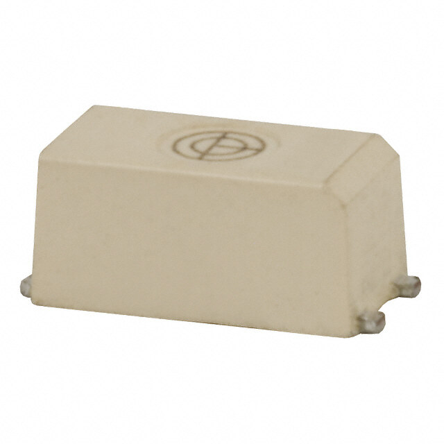
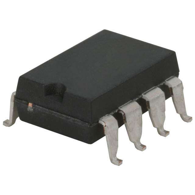
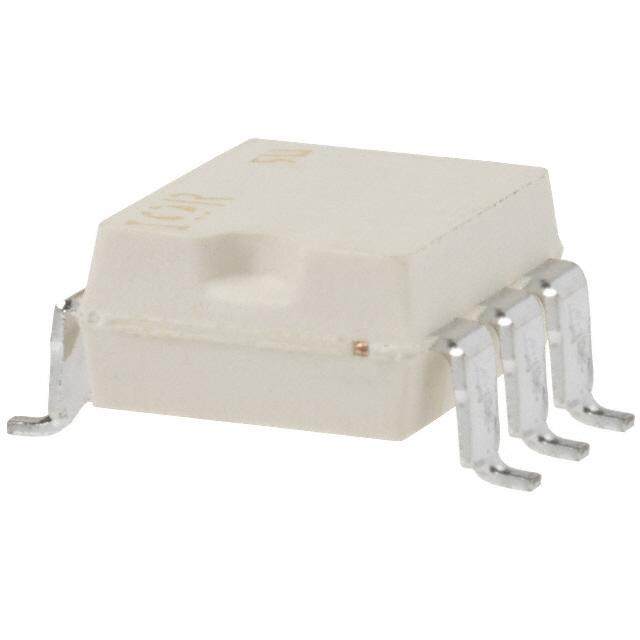
| 描述 | SSR OCMOS FET 600MA NO 4-SOP固态继电器-PCB安装 1-Ch Normally Open |
| 产品分类 | |
| 品牌 | CEL |
| 产品手册 | |
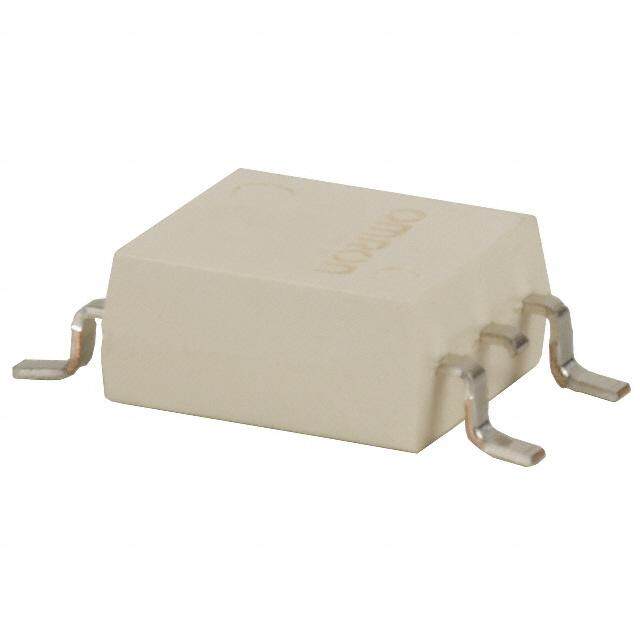
| 产品图片 |
|
| rohs | 符合RoHS无铅 / 符合限制有害物质指令(RoHS)规范要求 |
| 产品系列 | 固态继电器,固态继电器-PCB安装,CEL PS7206-1A-APS, OCMOS |
| 数据手册 | |
| 产品型号 | PS7206-1A-A |
| 产品 | Instrumentation Relays |
| 产品培训模块 | http://www.digikey.cn/PTM/IndividualPTM.page?site=cn&lang=zhs&ptm=14010 |
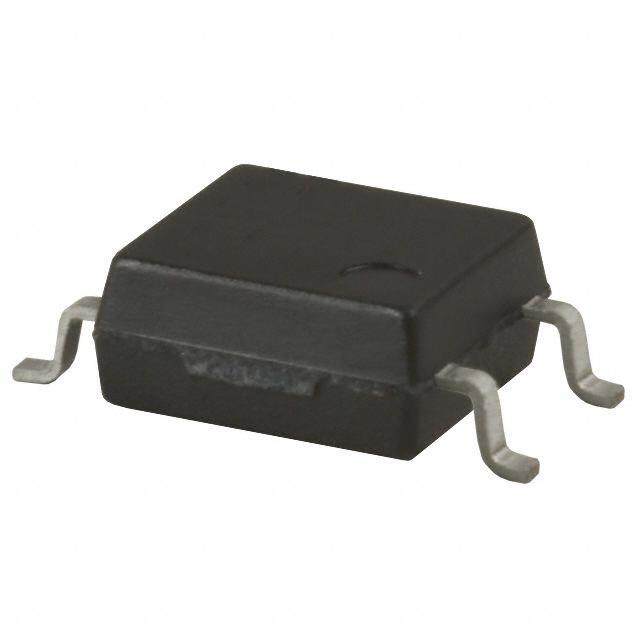
| 产品目录绘图 |
|
| 产品目录页面 | |
| 产品种类 | Solid State Relays |
| 产品类型 | PCB Mount |
| 供应商器件封装 | 4-SOP(2.54mm) |
| 其它名称 | PS7206-1AA |
| 包装 | 管件 |
| 商标 | CEL |
| 安装类型 | 表面贴装 |
| 安装风格 | SMD/SMT |
| 导通电阻 | 800 毫欧 |
| 封装 | Tube |
| 封装/外壳 | 4-SOP(0.173",4.40mm) |
| 封装/箱体 | SOP-4 |
| 工厂包装数量 | 100 |
| 标准包装 | 100 |
| 电压-负载 | 0 ~ 60 V |
| 电压-输入 | 1.2VDC |
| 电路 | SPST-NO(1 Form A) |
| 端子类型 | 鸥翼型 |
| 端接类型 | SMD/SMT |
| 系列 | PS |
| 继电器类型 | |
| 触点形式 | 1 Form A (SPST-NO) |
| 负载电压额定值 | 60 V |
| 负载电流 | 600mA |
| 负载电流额定值 | 600 mA |
| 输入电流 | 50 mA |
| 输入转输出绝缘方法 | Optocoupler |
| 输出类型 | AC,DC |
| 输出设备 | MOSFET |


- 商务部:美国ITC正式对集成电路等产品启动337调查
- 曝三星4nm工艺存在良率问题 高通将骁龙8 Gen1或转产台积电
- 太阳诱电将投资9.5亿元在常州建新厂生产MLCC 预计2023年完工
- 英特尔发布欧洲新工厂建设计划 深化IDM 2.0 战略
- 台积电先进制程称霸业界 有大客户加持明年业绩稳了
- 达到5530亿美元!SIA预计今年全球半导体销售额将创下新高
- 英特尔拟将自动驾驶子公司Mobileye上市 估值或超500亿美元
- 三星加码芯片和SET,合并消费电子和移动部门,撤换高东真等 CEO
- 三星电子宣布重大人事变动 还合并消费电子和移动部门
- 海关总署:前11个月进口集成电路产品价值2.52万亿元 增长14.8%


PDF Datasheet 数据手册内容提取
Solid State Relay OCMOS FET PS7206-1A 4-PIN SOP, 0.6 Ω LOW ON-STATE RESISTANCE D 600 mA CONTINUOUS LOAD CURRENT −NEPOC Series− 1-ch Optical Coupled MOS FET E DESCRIPTION The PS7206-1A is a low on-state resistance solid state relay containing GaAs LEDs on the light emitting side (input side) and MOS FETs on the output side. U It is suitable for PLC, etc. because of its large continuous load current and low on-state resistance. FEATURES • Low on-state resistance (Ron = 0.6 Ω TYP.) N • Large continuous load current (IL = 600 mA) PIN CONNECTION • 1 channel type (1 a output) (Top View) • Designed for AC/DC switching line changer 4 3 I • Small and thin package (4-pin SOP, Height = 2.1 mm) • High isolation voltage (BV = 1 500 Vr.m.s.) T 1.LED Anode 2.LED Cathode • Low offset voltage 3.MOS FET • Ordering number of taping product : PS7206-1A-E3, E4: 900 pcs/reel 4.MOS FET : PS7206-1A-F3, F4: 3 500 pcs/reel N • Pb-Free product 1 2 • Safety standards • UL approved: No. E72422 • BSI approved: No. 8241, 8242 O APPLICATIONS • Measurement equipment • FA equipment C S I D Document No. PN10297EJ03V0DS (3rd edition) Date Published February 2009 NS The mark <R> shows major revised points. The revised points can be easily searched by copying an "<R>" in the PDF file and specifying it in the "Find what:" field.
PS7206-1A PACKAGE DIMENSIONS (UNIT: mm) 4.0±0.5 D E U 7.0±0.3 4.4 N +0.0805–0.05 +0.100.15–0.05 2. I +0.085–0.05 2.54 T 0.5±0.3 0.0 0.40+–00..1005 0.25 M N <R> MARKING EXAMPLE (LASER MARKING) O 06-A Type Number N901 Assembly Lot *1 No.1 pin Mark C N 9 01 Week Assembled Year Assembled S (Last 1 Digit) Rank Code *1 Bar : Pb-Free I Remark Applicable type numbers are underlined below PS7206-1A D 2 Data Sheet PN10297EJ03V0DS
PS7206-1A ORDERING INFORMATION Part Number Order Number Solder Plating Packing Style Safety Standard Application Part Specification Approval Number*1 D PS7206-1A PS7206-1A-A Pb-Free Magazine case 100 pcs Standard products PS7206-1A PS7206-1A-E3 PS7206-1A-E3-A Embossed Tape 900 pcs/reel (UL, BSI approved) PS7206-1A-E4 PS7206-1A-E4-A E PS7206-1A-F3 PS7206-1A-F3-A Embossed Tape 3 500 pcs/reel PS7206-1A-F4 PS7206-1A-F4-A U *1 For the application of the Safety Standard, following part number should be used. ABSOLUTE MAXIMUM RATINGS (TA = 25°C, unless otherwise specified) N Parameter Symbol Ratings Unit Diode Forward Current (DC) IF 50 mA Reverse Voltage VR 5.0 V I Power Dissipation PD 50 mW T Peak Forward Current *1 IFP 1 A MOS FET Break Down Voltage VL 60 V Continuous Load Current IL N600 mA Pulse Load Current *2 ILP 1.2 A (AC/DC Connection) Power Dissipation PD 300 mW O Isolation Voltage *3 BV 1500 Vr.m.s. Total Power Dissipation PT 350 mW Operating Ambient Temperature TA −40 to +85 °C Storage Temperature CTstg −40 to +100 °C *1 PW = 100 µs, Duty Cycle = 1% *2 PW = 100 ms, 1 shot S *3 AC voltage for 1 minute at TA = 25°C, RH = 60% between input and output. Pins 1-2 shorted together, 3-4 shorted together. I D Data Sheet PN10297EJ03V0DS 3
PS7206-1A RECOMMENDED OPERATING CONDITIONS (TA = 25°C) Parameter Symbol MIN. TYP. MAX. Unit LED Operating Current IF 2 10 20 mA D LED Off Voltage VF 0 0.5 V ELECTRICAL CHARACTERISTICS (TA = 25°C) E Parameter Symbol Conditions MIN. TYP. MAX. Unit Diode Forward Voltage VF IF = 10 mA 1.2 1.4 V U Reverse Current IR VR = 5 V 5.0 µA MOS FET Off-state Leakage Current ILoff VD = 60 V 1.0 µA Output Capacitance Cout VD = 0 V, f = 1 MHz 70 pF N Coupled LED On-state Current IFon IL = 600 mA 2.0 mA <R> On-state Resistance Ron1 IF = 10 mA, IL = 100 mA 0.6 0.8 Ω Ron2 IF = 10 mA, IL = 600 mA, t ≤ 10 ms 0.6 0.8 I Turn-on Time*1, 2 ton IF = 10 mA, VO = 5 V, RL = 500 Ω, 0.4 2.0 ms Turn-off Time*1, 2 toff PW ≥ 10 ms T 0.08 0.5 Isolation Resistance RI-O VI-O = 1.0 kVDC 109 Ω Isolation Capacitance CI-O V = 0 V, f = 1 MHz 0.5 pF N *1 Test Circuit for Switching Time IF O Pulse Input VL Input 50 % 0 C VO = 5 V 90 % Input monitor VOmonitor Output SRin RL 10 % ton toff *2 The tuIrn-on time and turn-off time are specified as input-pulse width ≥ 10 ms. Be aware that when the device operates with an input-pulse width less than 10 ms, the turn-on time and turn-off D time will increase. 4 Data Sheet PN10297EJ03V0DS
PS7206-1A TYPICAL CHARACTERISTICS (TA = 25°C, unless otherwise specified) MAXIMUM FORWARD CURRENT vs. MAXIMUM LOAD CURRENT vs. AMBIENT TEMPERATURE AMBIENT TEMPERATURE 100 900 D A) m A) ent I (F 80 nt I (mL 600 E Curr 60 urre d C ar d w a or 40 Lo F m 300 U m u u m m 20 xi axi Ma M 0 0 –25 0 25 50 75 85 100 –25 N0 25 50 75 85 100 Ambient Temperature TA (°C) Ambient Temperature TA (°C) FORWARD VOLTAGE vs. OUTPUT CAPACITANCE vs. AMBIENT TEMPERATURE IAPPLIED VOLTAGE 1.8 200 T f = 1 MHz Voltage V (V)F 11..46 IF = 5321000051 mmmmmmAAAAAA N acitance C (pF)out 115000 d 1.2 p ar Ca Forw 1.0 O utput 50 O 0.8 –25 0 25 50 75 100 0 20 40 60 80 100 120 C Ambient Temperature TA (°C) Applied Voltage VD (V) OFF-STATE LEAKAGE CURRENT vs. AMBIENT TEMPERATURE LOAD CURRENT vs. LOAD VOLTAGE 10–6 S 900 nt I (A)Loff 10–7 I VD = 60 V mA) IIFL == 61000 m mAA, 600 e Curre 10–8D ent I (L 300 akag 10–9 Curr –0.8 –0.4 0 0.4 0.8 e Le oad –300 Off-stat10–10 L –600 10–11 –900 0 20 40 60 80 Ambient Temperature TA (°C) Load Voltage VL (V) Remark The graphs indicate nominal characteristics. Data Sheet PN10297EJ03V0DS 5
PS7206-1A NORMALIZED ON-STATE RESISTANCE vs. AMBIENT TEMPERATURE ON-STATE RESISTANCE DISTRIBUTION 3.0 30 Resistance Ron 22..05 IINaFLt o ==Tr mA61 00=a0 l mi2 zm5eA°dA,C t,o 1.0 pcs) 2205 InItFL = == 1 5610000 m 0 pm scmDAsA,, ate 1.5 er ( 15 E d On-st 1.0 Numb 10 e z mali 0.5 5 U or N 0.0 0 –25 0 25 50 75 100 0.4 0.6 0.8 Ambient Temperature TA (°C) On-state Resistance Ron (Ω) N TURN-ON TIME vs. FORWARD CURRENT TURN-OFF TIME vs. FORWARD CURRENT 3.0 0.30 VO = 5 V, I VO = 5 V, RL = 500 Ω RL = 500 Ω 2.5 0.25 T s) s) m m e t (on 2.0 e t (off 0.20 m 1.5 m0.15 Ti N Ti on off n- 1.0 n-0.10 ur ur T T 0.5 0.05 O 0 5 10 15 20 25 30 0 5 10 15 20 25 30 Forward Current IF (mA) Forward Current IF (mA) C TURN-ON TIME DISTRIBUTION TURN-OFF TIME DISTRIBUTION 30 30 n = 50 pcs, n = 50 pcs, 25 S IVF O= = 1 50 Vm,A, 25 IVF O= = 1 50 Vm,A, RL = 500 Ω RL = 500 Ω s) 20 s) 20 c c p p er ( 15 I er ( 15 b b m m u D u N 10 N 10 5 5 0 0 0.4 0.6 0.08 0.12 Turn-on Time ton (ms) Turn-off Time toff (ms) Remark The graphs indicate nominal characteristics. 6 Data Sheet PN10297EJ03V0DS
PS7206-1A NORMALIZED TURN-ON TIME vs. NORMALIZED TURN-OFF TIME vs. AMBIENT TEMPERATURE AMBIENT TEMPERATURE 3.0 3.0 Normalized to 1.0 Normalized to 1.0 at TA = 25°C, at TA = 25°C, Time ton 22..50 IVRF OL= == 1 5500 Vm0 AΩ, Time toff 22..50 IVRF OL= == 1 5500 Vm0, AΩ, D Turn-on 1.5 Turn-off 1.5 E malized 1.0 malized 1.0 Nor 0.5 Nor 0.5 U 0.0 0.0 –25 0 25 50 75 100 –25 0 25 50 75 100 Ambient Temperature TA (°C) Ambient Temperature TA (°C) N Remark The graphs indicate nominal characteristics. I T N O C S I D Data Sheet PN10297EJ03V0DS 7
PS7206-1A TAPING SPECIFICATIONS (in millimeters) D Outline and Dimensions (Tape) 1 0. 2.0±0.05 ± 5 4.0±0.1 1.5+–00. 1 1.7 2.9 MAX. E 5 2 5.5±0.0 12.0±0. 7.4±0.1 U 1.55±0.1 4.6±0.1 2.4±0.1 8.0±0.1 0.3 N Tape Direction I T PS7206-1A-E3 PS7206-1A-E4 N O Outline and Dimensions (Reel) 2.0±0.5 C 2.0±0.5 φ13.0±0.2 S φ+0 180–1.5 +160–0 R 1.0 φ φ21.0±0.8 I 13.5±1.0 D 17.5±1.0 11.9 to 15.4 Outer edge of Packing: 900 pcs/reel flange 8 Data Sheet PN10297EJ03V0DS
PS7206-1A Outline and Dimensions (Tape) D 1 0. 2.0±0.05 ± 5 4.0±0.1 1.5+–00. 1 1.7 2.9 MAX. 5 2 E 5.5±0.0 12.0±0. 7.4±0.1 1.55±0.1 4.6±0.1 2.4±0.1 U 8.0±0.1 0.3 N Tape Direction PS7206-1A-F3 IPS7206-1A-F4 T N Outline and DimensionOs (Reel) 2.0±0.5 C 2.0±0.5 φ13.0±0.2 0 0±2. 1.0 0.2 S 3 ± ± 3 0 0 R 1.0 φ21.0±0.8 φ φ10 φ13. 13.5±1.0 I 17.5±1.0 D 11.9 to 15.4 Outer edge of Packing: 3 500 pcs/reel flange Data Sheet PN10297EJ03V0DS 9
PS7206-1A RECOMMENDED SOLDERING CONDITIONS (1)Infrared reflow soldering • Peak reflow temperature 260°C or below (package surface temperature) • Time of peak reflow temperature 10 seconds or less D • Time of temperature higher than 220°C 60 seconds or less • Time to preheat temperature from 120 to 180°C 120±30 s • Number of reflows Three • Flux Rosin flux containing small amount of chlorineE (The flux with a maximum chlorine content of 0.2 Wt% is recommended.) Recommended Temperature Profile of Infrared Reflow U C) ° (heating)N T ( to 10 s e ur 260°C MAX. erat 220°C p m to 60 s e I T ace 180°C T Surf 120°C ge 120±30 s ka (preheating) c a N P O Time (s) (2)Wave soldering • Temperature 260°C or below (molten solder temperature) C • Time 10 seconds or less • Preheating conditions 120°C or below (package surface temperature) • Number of times One • Flux SRosin flux containing small amount of chlorine (The flux with a maximum chlorine content of 0.2 Wt% is recommended.) (3)Soldering by soldering iron I • Peak temperature (lead part temperature) 350°C or below • TimDe (each pins) 3 seconds or less • Flux Rosin flux containing small amount of chlorine (The flux with a maximum chlorine content of 0.2 Wt% is recommended.) (a)Soldering of leads should be made at the point 1.5 to 2.0 mm from the root of the lead. (b)Please be sure that the temperature of the package would not be heated over 100°C. (4)Cautions • Fluxes Avoid removing the residual flux with freon-based and chlorine-based cleaning solvent. 10 Data Sheet PN10297EJ03V0DS
PS7206-1A USAGE CAUTIONS 1. Protect against static electricity when handling. 2. Avoid storage at a high temperature and high humidity. D E U N I T N O C S I D Data Sheet PN10297EJ03V0DS 11
PS7206-1A This product uses gallium arsenide (GaAs). Caution GaAs Products GaAs vapor and powder are hazardous to human health if inhaled or ingested, so please observe the following points. •Follow related laws and ordinances when disposing of the product. If there are no applicable laws and/or ordinances, dispose of the product as recommended below. D 1.Commission a disposal company able to (with a license to) collect, transport and dispose of materials that contain arsenic and other such industrial waste materials. 2.Exclude the product from general industrial waste and household garbage, and ensure that the product is controlled (as industrial waste subject to special control) up until finEal disposal. •Do not burn, destroy, cut, crush, or chemically dissolve the product. •Do not lick the product or in any way allow it to enter the mouth. U N I T N O C S I D
NOTICE 1. Descriptions of circuits, software and other related information in this document are provided only to illustrate the operation of semiconductor products and application examples. You are fully responsible for the incorporation of these circuits, software, and information in the design of your equipment. California Eastern Laboratories and Renesas Electronics assumes no responsibility for any losses incurred by you or third parties arising from the use of thDese circuits, software, or information. 2. California Eastern Laboratories has used reasonable care in preparing the information included in this document, but California Eastern Laboratories does not warrant that such information is error free. California Eastern Laboratories and Renesas Electronics assumes no liability whatsoever for any damages incurred by you resulting from errors in or omissions from the information included herein. 3. California Eastern Laboratories and Renesas Electronics do not assume any liability for infringement of patents, copyrights, or other intellectual property E rights of third parties by or arising from the use of Renesas Electronics products or technical information described in this document. No license, express, implied or otherwise, is granted hereby under any patents, copyrights or other intellectual property rights of California Eastern Laboratories or Renesas Electronics or others. 4. You should not alter, modify, copy, or otherwise misappropriate any Renesas Electronics product, whether in whole or in part. California Eastern Laboratories and Renesas Electronics assume no responsibility for any losses incurred by you or third parties arising from such alteration, modification, copy or otherwise misappropriation of Renesas Electronics product. U 5. Renesas Electronics products are classified according to the following two quality grades: “Standard” and “High Quality”. The recommended applications for each Renesas Electronics product depends on the product’s quality grade, as indicated below. “Standard”: Computers; office equipment; communications equipment; test and measurement equipment; audio and visual equipment; home electronic appliances; machine tools; personal electronic equipment; and industrial robots etc. “High Quality”: Transportation equipment (automobiles, trains, ships, etc.); traffic control systems; anti-disaster systems; anti-crime systems; and safety equipment etc. Renesas Electronics products are neither intended nor authorized foNr use in products or systems that may pose a direct threat to human life or bodily injury (artificial life support devices or systems, surgical implantations etc.), or may cause serious property damages (nuclear reactor control systems, military equipment etc.). You must check the quality grade of each Renesas Electronics product before using it in a particular application. You may not use any Renesas Electronics product for any application for which it is not intended. California Eastern Laboratories and Renesas Electronics shall not be in any way liable for any damages or losses incurred by you or third parties arising from the use of any Renesas Electronics product for which the product is not intended by California Eastern Laboratories or Renesas Electronics. 6. You should use the Renesas Electronics products described in this document within the rIange specified by California Eastern Laboratories, especially with respect to the maximum rating, operating supply voltage range, movement power voltage range, heat radiation characteristics, installation and other product characteristics. California Eastern Laboratories shall have no liability for malfunctiTons or damages arising out of the use of Renesas Electronics products beyond such specified ranges. 7. Although Renesas Electronics endeavors to improve the quality and reliability of its products, semiconductor products have specific characteristics such as the occurrence of failure at a certain rate and malfunctions under certain use conditions. Further, Renesas Electronics products are not subject to radiation resistance design. Please be sure to implement safety measures to guard them against the possibility of physical injury, and injury or damage caused by N fire in the event of the failure of a Renesas Electronics product, such as safety design for hardware and software including but not limited to redundancy, fire control and malfunction prevention, appropriate treatment for aging degradation or any other appropriate measures. Because the evaluation of microcomputer software alone is very difficult, please evaluate the safety of the final products or systems manufactured by you. 8. Please contact a California Eastern Laboratories sales office for details as to environmental matters such as the environmental compatibility of each Renesas Electronics product. Please use Renesas Electronics products in compliance with all applicable laws and regulations that regulate the inclusion or use of controlled substances, including without limitation, the EOU RoHS Directive. California Eastern Laboratories and Renesas Electronics assume no liability for damages or losses occurring as a result of your noncompliance with applicable laws and regulations. 9. Renesas Electronics products and technology may not be used for or incorporated into any products or systems whose manufacture, use, or sale is prohibited under any applicable domestic or foreign laws or regulations. You should not use Renesas Electronics products or technology described in this document for any purpose relating to military applications or use by the military, including but not limited to the development of weapons of mass destruction. When exporting the Renesas Electronics products or technology described in this document, you should comply with the applicable export control laws and regulations and follow the procedures requCired by such laws and regulations. 10. It is the responsibility of the buyer or distributor of California Eastern Laboratories, who distributes, disposes of, or otherwise places the Renesas Electronics product with a third party, to notify such third party in advance of the contents and conditions set forth in this document, California Eastern Laboratories and Renesas Electronics assume no responsibility for any losses incurred by you or third parties as a result of unauthorized use of Renesas Electronics products. 11. This document may not be reproduced or duplicated in any form, in whole or in part, without prior written consent of California Eastern Laboratories. 12. Please contact a California Eastern Laboratories sales office if you have any questions regarding the information contained in this document or Renesas S Electronics products, or if you have any other inquiries. NOTE 1: “Renesas Electronics” as used in this document means Renesas Electronics Corporation and also includes its majority-owned subsidiaries. NOTE 2: “Renesas Electronics product(s)” means any product developed or manufactured by or for Renesas Electronics. NOTE 3: Products and product information are subject to change without notice. I D CEL Headquarters • 4590 Patrick Henry Drive, Santa Clara, CA 95054 • Phone (408) 919-2500 • www.cel.com For a complete list of sales offices, representatives and distributors, Please visit our website: www.cel.com/contactus