 Datasheet下载
- 型号: PS7122AL-1A-A
- 制造商: CEL
- 库位|库存: xxxx|xxxx
- 要求:
| 数量阶梯 | 香港交货 | 国内含税 |
| +xxxx | $xxxx | ¥xxxx |
查看当月历史价格
查看今年历史价格
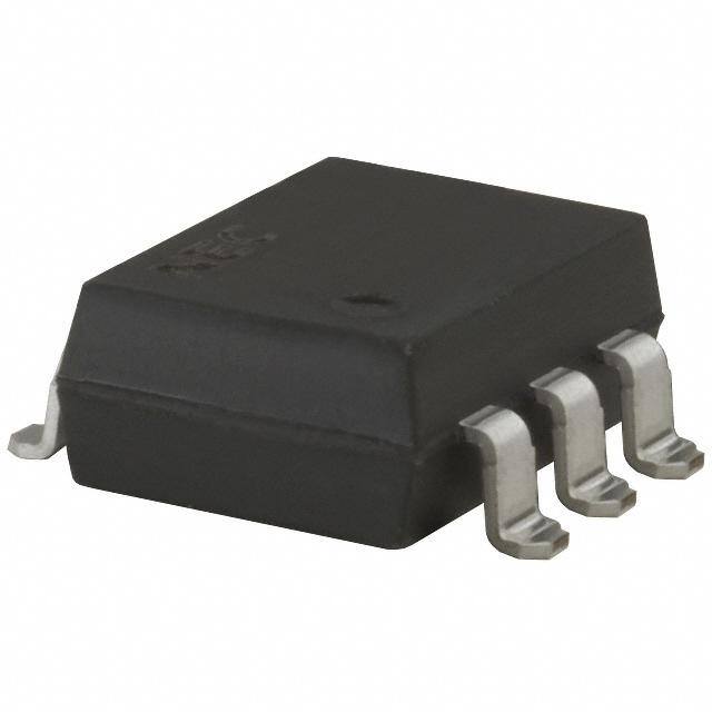
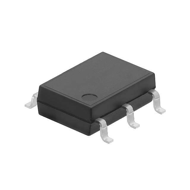
PS7122AL-1A-A产品简介:
ICGOO电子元器件商城为您提供PS7122AL-1A-A由CEL设计生产,在icgoo商城现货销售,并且可以通过原厂、代理商等渠道进行代购。 PS7122AL-1A-A价格参考。CELPS7122AL-1A-A封装/规格:固态继电器, Solid State Relay SPST-NO (1 Form A) 6-SMD (0.300", 7.62mm)。您可以下载PS7122AL-1A-A参考资料、Datasheet数据手册功能说明书,资料中有PS7122AL-1A-A 详细功能的应用电路图电压和使用方法及教程。
CEL PS7122AL-1A-A是一款固态继电器(SSR),属于无触点电子开关器件,具有高可靠性、长寿命和低噪声等优点。该型号采用光耦隔离技术,输入与输出之间电气隔离良好,适用于需要安全控制和抗干扰能力强的场合。

其典型应用场景包括:工业自动化控制系统中用于驱动交流负载,如加热器、电机、电磁阀和小型交流电动机的通断控制;在温度控制系统中作为加热回路的开关元件,广泛应用于塑料机械、包装设备、食品加工设备等;也可用于电源切换、照明控制及各类电器中的负载管理。

PS7122AL-1A-A支持交流输出,额定负载电流为1A,适合中小功率交流负载控制。由于其输入控制电压范围宽(通常为3–32VDC),可直接与PLC、单片机、微控制器等逻辑电路接口兼容,无需额外驱动电路,简化系统设计。

此外,该器件具备良好的耐浪涌能力和过零触发功能,可有效减少开关瞬间对电网和负载的冲击,提升系统稳定性和电磁兼容性。因此,它特别适用于对运行稳定性要求较高的环境,如精密仪器、医疗设备和通信电源系统。

综上所述,CEL PS7122AL-1A-A固态继电器广泛应用于工业控制、自动化设备、温控系统及各类需安全可靠开关交流负载的电子装置中。
| 参数 | 数值 |
| 产品目录 | |
| 描述 | SSR OCMOS FET 200MA 1CH NO 6-SMD |
| 产品分类 | |
| 品牌 | CEL |
| 数据手册 | |
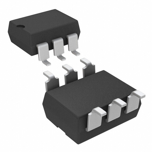
| 产品图片 |
|
| 产品型号 | PS7122AL-1A-A |
| rohs | 无铅 / 符合限制有害物质指令(RoHS)规范要求 |
| 产品系列 | PS, OCMOS |
| 产品目录绘图 |
|
| 产品目录页面 | |
| 供应商器件封装 | 6-DIP 鸥翼型 |
| 其它名称 | PS7122AL-1A |
| 包装 | 管件 |
| 安装类型 | 表面贴装 |
| 导通电阻 | 8 欧姆 |
| 封装/外壳 | 6-SMD(0.300",7.62mm) |
| 标准包装 | 50 |
| 电压-负载 | 0 ~ 250 V |
| 电压-输入 | 1.2VDC |
| 电路 | SPST-NO(1 A 形) |
| 端子类型 | 鸥翼型 |
| 继电器类型 | |
| 负载电流 | 200mA |
| 输出类型 | AC,DC |


.jpg)

- 商务部:美国ITC正式对集成电路等产品启动337调查
- 曝三星4nm工艺存在良率问题 高通将骁龙8 Gen1或转产台积电
- 太阳诱电将投资9.5亿元在常州建新厂生产MLCC 预计2023年完工
- 英特尔发布欧洲新工厂建设计划 深化IDM 2.0 战略
- 台积电先进制程称霸业界 有大客户加持明年业绩稳了
- 达到5530亿美元!SIA预计今年全球半导体销售额将创下新高
- 英特尔拟将自动驾驶子公司Mobileye上市 估值或超500亿美元
- 三星加码芯片和SET,合并消费电子和移动部门,撤换高东真等 CEO
- 三星电子宣布重大人事变动 还合并消费电子和移动部门
- 海关总署:前11个月进口集成电路产品价值2.52万亿元 增长14.8%
.jpg)
PDF Datasheet 数据手册内容提取
Solid State Relay OCMOS FET PS7122A-1A,-2A,PS7122AL-1A,-2A 6, 8-PIN DIP, 250 V BREAK DOWN VOLTAGE D NORMALLY OPEN TYPE −NEPOC Series− 1-ch, 2-ch Optical Coupled MOS FET E DESCRIPTION The PS7122A-1A, -2A and PS7122AL-1A, -2A are solid state relays containing GaAs LEDs on the light emitting U side (input side) and MOS FETs on the output side. They are suitable for analog signal control because of their low offset and high linearity. The PS7122AL-1A, -2A have a surface mount type lead. N FEATURES • 1 channel type (1 a output) or 2 channel type (1 a + 1 a output) • Low LED operating current (IF = 2 mA) • Designed for AC/DC switching line changer I • Small package (6, 8-pin DIP) T • Low offset voltage • Ordering number of taping product : PS7122AL-1A-E3, E4: 1 000 pcs/reel : PS7122AL-2A-E3, E4: 1 000 pcs/reel N <R> • Pb-Free product • Safety standards • UL approved: File No. E72422 • BSI approved: No. 8245/8246 O • CSA approved: No. CA 101391 APPLICATIONS • Exchange equipment C • Measurement equipment • FA/OA equipment S I D Document No. PN10273EJ02V0DS (2nd edition) Date Published July 2006 NS CP(K) The mark <R> shows major revised points. 1997, 2006 The revised points can be easily searched by copying an "<R>" in the PDF file and specifying it in the "Find what:" field.
PS7122A-1A,-2A,PS7122AL-1A,-2A PACKAGE DIMENSIONS (in millimeters) D PS7122A-1A PS7122AL-1A TOP VIEW TOP VIEW 9.25±0.5 6 5 4 9.25±0.5 6 5 4 E 1 2 3 U 1 2 3 1. LED Anode 1. LED Anode 2. LED Cathode 2. LED Cathode 3. NC 3. NC 4. MOS FET Drain 4. MOS FET Drain 5. MOS FET Source 5. MOS FET Source 6. MOS FET Drain N 6. MOS FET Drain 7.62 6.5±0.5 6.5±0.5 4.15±0.3 3.5±0.3 T3.5±0.3I +0.100.10–0.05 3 0.9±0.25 0. 1.34±0.1 2.54 ± 3.3 0.25 M 9.60±0.4 0 to 15˚ N 0.5±0.1 1.34±0.1 2.54 0.25 M O PS7122A-2A PS7122AL-2A TOP VIEW TOP VIEW 9.25±0.5 8 7 6 5 9.25±0.5 8 7 6 5 C S 1 2 3 4 1 2 3 4 1. LED Anode 5. MOS FET 1. LED Anode 5. MOS FET 2. LED Cathode 6. MOS FET 2. LED Cathode 6. MOS FET 3. LED Anode 7. MOS FET 3. LED Anode 7. MOS FET 4. LED Cathode 8. MOS FET 4. LED Cathode 8. MOS FET I 7.62 D 6.5±0.5 6.5±0.5 5±0.3 5±0.3 5±0.3 +0.100.10–0.05 4.1 3. 3. 3 0.9±0.25 ±0. 1.34±0.1 2.54 3 3. 0.25 M 9.60±0.4 0.5±0.1 0 to 15˚ 1.34±0.1 2.54 0.25 M 2 Data Sheet PN10273EJ02V0DS
PS7122A-1A,-2A,PS7122AL-1A,-2A <R> MARKING EXAMPLE PS7122A-1A PS7122A-2A D No. 1 pin No. 1 pin Mark Country Assembled Mark Country Assembled PS7122A-1A Type Number PS7122A-2A EType Number NL601 Assembly Lot NL601 Assembly Lot U N L 6 01 N L 6 01 Week Assembled Week Assembled Year Assembled Year Assembled (Last 1 Digit) N (Last 1 Digit) In-house Code In-house Code (L: Pb-Free) (L: Pb-Free) Rank Code Rank Code I T N O C S I D Data Sheet PN10273EJ02V0DS 3
PS7122A-1A,-2A,PS7122AL-1A,-2A <R> ORDERING INFORMATION Part Number Order Number Solder Plating Packing Style Safety Standard Application Specification Approval Part NuDmber*1 PS7122A-1A PS7122A-1A-A Pb-Free Magazine case 50 pcs Standard products PS7122A-1A PS7122AL-1A PS7122AL-1A-A (UL, BSI, CSA PS7122AL-1A-E3 PS7122AL-1A-E3-A Embossed Tape 1 000 pcs/reel approved) E PS7122AL-1A-E4 PS7122AL-1A-E4-A PS7122A-2A PS7122A-2A-A Magazine case 50 pcs PS7122A-2A U PS7122AL-2A PS7122AL-2A-A PS7122AL-2A-E3 PS7122AL-2A-E3-A Embossed Tape 1 000 pcs/reel PS7122AL-2A-E4 PS7122AL-2A-E4-A N *1 For the application of the Safety Standard, following part number should be used. I T N O C S I D 4 Data Sheet PN10273EJ02V0DS
PS7122A-1A,-2A,PS7122AL-1A,-2A ABSOLUTE MAXIMUM RATINGS (TA = 25°C, unless otherwise specified) Ratings D Parameter Symbol PS7122A-1A, PS7122A-2A, Unit PS7122AL-1A PS7122AL-2A Diode Forward Current (DC) IF 50 mA/ch Reverse Voltage VR 5.0 V E Power Dissipation PD 50 mW/ch Peak Forward Current *1 IFP 1 A/ch U MOS FET Break Down Voltage VL 250 V Continuous Connection A IL 200 mA/ch Load Current *2 Connection B 350 − N Connection C 500 − Pulse Load Current *3 ILP 400 mA/ch (AC/DC Connection) Power Dissipation PD 560 I375 mW/ch Isolation Voltage *4 BV 1 500 Vr.m.s. T Total Power Dissipation PT 610 850 mW Operating Ambient Temperature TA −40 to +85 °C Storage Temperature Tstg N −40 to +100 °C *1 PW = 100 µs, Duty Cycle = 1% *2 Conditions: IF ≥ 2 mA. The following types of load connections are available. O 6 1 Connection A 2 5 VL (AC/DC) 3 IL L 4 6 C 1 L + 2 5 IL – VL (DC) 3 4 Connection B 1 6 2 – S 3 54 IL L + VL (DC) 1 6 IL L + Connection C 2 5 – VL (DC) 3 IL + IL 4 IL I *3 DPW = 100 ms, 1 shot *4 AC voltage for 1 minute at TA = 25°C, RH = 60% between input and output Pins 1-3 shorted together, 4-6 shorted together. (PS7122A-1A) Pins 1-4 shorted together, 5-8 shorted together. (PS7122A-2A) Data Sheet PN10273EJ02V0DS 5
PS7122A-1A,-2A,PS7122AL-1A,-2A RECOMMENDED OPERATING CONDITIONS (TA = 25°C) Parameter Symbol MIN. TYP. MAX. Unit D LED Operating Current IF 2 10 20 mA LED Off Voltage VF 0 0.5 V E ELECTRICAL CHARACTERISTICS (TA = 25°C) Parameter Symbol Conditions MIN. TYP. MAX. Unit Diode Forward Voltage VF IF = 10 mA U1.2 1.4 V Reverse Current IR VR = 5 V 5.0 µA MOS FET Off-state Leakage ILoff VD = 250 V 0.03 1.0 µA Current N Output Capacitance Cout VD = 0 V, f = 1 MHz 120 pF/ch Coupled LED On-state Current IFon IL = 200 mA 2.0 mA On-state Resistance Ron1 IF = 10 mA, IL = 10 mA 4.5 8.0 Ω I Ron2 IF = 10 mA, IL = 200 mA, t ≤ 10 ms T Turn-on Time *1, 2 ton IF = 10 mA, VO = 5 V, RL = 500 Ω, 0.5 1.5 ms Turn-off Time *1, 2 toff PW ≥ 10 ms 0.04 0.2 Isolation Resistance RI-O VI-O = 1N.0 kVDC 109 Ω Isolation Capacitance CI-O V = 0 V, f = 1 MHz 1.1 pF/ch *1 Test Circuit for Switching Time O IF Pulse Input VL Input 50 % 0 C VO = 5 V 90 % Input monitor VOmonitor S Output Rin RL 10 % ton toff I <R> *2 DThe turn-on time and turn-off time are specified as input-pulse width ≥ 10 ms. Be aware that when the device operates with an input-pulse width less than 10 ms, the turn-on time and turn-off time will increase. 6 Data Sheet PN10273EJ02V0DS
PS7122A-1A,-2A,PS7122AL-1A,-2A TYPICAL CHARACTERISTICS (TA = 25°C, unless otherwise specified) MAXIMUM FORWARD CURRENT vs. MAXIMUM LOAD CURRENT vs. AMBIENT TEMPERATURE AMBIENT TEMPERATURE D 100 300 A) m A) ent I (F 80 nt I (mL 200 E Curr 60 urre d C ar d orw 40 Loa U F m 100 m u u m m 20 xi axi Ma M 0 0 N –25 0 25 50 7585 100 –25 0 25 50 7585 100 Ambient Temperature TA (˚C) Ambient Temperature TA (˚C) FORWARD VOLTAGE vs. OUTPUT CAPACITANCE vs. I AMBIENT TEMPERATURE APPLIED VOLTAGE 1.6 T400 f = 1 MHz F) V (V)F 1.4 N C (pout 300 Voltage 1.2 IF = 235000 mmmAAA acitance 200 ard O10 mA Cap Forw 1.0 51 mmAA utput 100 O 0.8 –25 0 25 C50 75 100 0 20 40 60 80 100 120 Ambient Temperature TA (˚C) Applied Voltage VD (V) OFF-STATE LEAKAGE CURRENT vs. APPLIEDS VOLTAGE LOAD CURRENT vs. LOAD VOLTAGE 10–5 IF =10 mA A) 200 nt I (Loff 10–6ITA = 85 ˚C mA) 100 e Curre D10–7 ent I (L ate Leakag 10–8 25 ˚C Load Curr –2.0 –1.0 0 –100 1.0 2.0 st Off- –200 10–9 0 50 100 150 200 250 Applied Voltage VD (V) Load Voltage VL (V) Remark The graphs indicate nominal characteristics. Data Sheet PN10273EJ02V0DS 7
PS7122A-1A,-2A,PS7122AL-1A,-2A NORMALIZED ON-STATE RESISTANCE vs. AMBIENT TEMPERATURE ON-STATE RESISTANCE DISTRIBUTION 3.0 30 Ron Normalized to 1.0 n = 50D pcs, nce 2.5 IaFt =T A1 0= m25A ˚, C, 25 IIFL == 1100 mmAA, Resista 2.0 IL = 10 mA pcs) 20 ate 1.5 er ( 15 E d On-st 1.0 Numb 10 e maliz 0.5 5 U or N 0.0 0 –25 0 25 50 75 100 4.3 4.4 4.5 4.6 4.7 Ambient Temperature TA (˚C) NOn-state Resistance Ron (Ω) TURN-ON TIME vs. FORWARD CURRENT TURN-OFF TIME vs. FORWARD CURRENT 12 I0.6 VO = 5 V VO = 5 V 10 T0.5 s) s) m m e t (on 8 N e t (off 0.4 m 6 m 0.3 Ti Ti on off n- 4 n- 0.2 ur ur T T 2 O 0.1 0 5 10 15 20 25 30 0 5 10 15 20 25 30 Forward Current IF (mA) Forward Current IF (mA) C TURN-ON TIME DISTRIBUTION TURN-OFF TIME DISTRIBUTION 30 30 S n = 50 pcs, n = 50 pcs, 25 IF = 10 mA, 25 IF = 10 mA, VO = 5 V VO = 5 V s) 20 s) 20 c c p I p er ( 15 er ( 15 b D b m m u u N 10 N 10 5 5 0 0 0.4 0.6 0.03 0.04 0.05 0.06 Turn-on Time ton (ms) Turn-off Time toff (ms) Remark The graphs indicate nominal characteristics. 8 Data Sheet PN10273EJ02V0DS
PS7122A-1A,-2A,PS7122AL-1A,-2A NORMALIZED TURN-ON TIME vs. NORMALIZED TURN-OFF TIME vs. AMBIENT TEMPERATURE AMBIENT TEMPERATURE 3.0 3.0 Normalized to 1.0 Normalized to 1.0 D at TA = 25 ˚C, at TA = 25 ˚C, me ton 2.5 IVF O= = 1 50 VmA, me toff 2.5 IVF O= = 1 50 VmA, Ti 2.0 Ti 2.0 Turn-on 1.5 Turn-off 1.5 E malized 1.0 malized 1.0 Nor 0.5 Nor 0.5 U 0.0 0.0 –25 0 25 50 75 100 –25 0 25 50 75 100 Ambient Temperature TA (˚C) NAmbient Temperature TA (˚C) Remark The graphs indicate nominal characteristics. I T N O C S I D Data Sheet PN10273EJ02V0DS 9
PS7122A-1A,-2A,PS7122AL-1A,-2A TAPING SPECIFICATIONS (in millimeters) D Outline and Dimensions (Tape) 1 0. 2.0±0.1 5± 7 4.0±0.1 1.5+–00.1 1. 4.5E MAX. 1 0. 3 7.5± 0±0. ±0.1 16. 0.3 U 1 1.55±0.1 10.4±0.1 4.0±0.1 12.0±0.1 N 0.3 I Tape Direction T PS7122AL-1A-E3 PS7122AL-1A-E4 PS7122AL-2A-E3 PS7122AL-2A-E4 N O Outline and Dimensions (Reel) 2.0±0.5 C 2.0±0.5 S 13.0±0.2 0 0 2. 1. ± ± 0 0 3 0 I R 1.0 3 1 21.0±0.8 17.5±1.0 D 21.5±1.0 15.9 to 19.4 Outer edge of Packing: 1 000 pcs/reel flange 10 Data Sheet PN10273EJ02V0DS
PS7122A-1A,-2A,PS7122AL-1A,-2A RECOMMENDED SOLDERING CONDITIONS (1) Infrared reflow soldering • Peak reflow temperature 260°C or below (package surface temperature) D • Time of peak reflow temperature 10 seconds or less • Time of temperature higher than 220°C 60 seconds or less • Time to preheat temperature from 120 to 180°C 120±30 s • Number of reflows Three E • Flux Rosin flux containing small amount of chlorine (The flux with a maximum chlorine content of 0.2 Wt% is recommended.) Recommended Temperature Profile of Infrared RUeflow C) N T (˚ (htoe a1t0in sg) e ur 260˚C MAX. erat 220˚C p I m to 60 s e T e T c 180˚C a urf S 120˚C ge 120±30 s ka (preheating)N c a P O Time (s) (2) Wave soldering C • Temperature 260°C or below (molten solder temperature) • Time 10 seconds or less • Preheating conditions 120°C or below (package surface temperature) • Number of timeSs One • Flux Rosin flux containing small amount of chlorine (The flux with a maximum chlorine content of 0.2 Wt% is recommended.) <R> (3) SoldeIring by soldering iron • PDeak temperature (lead part temperature) 350°C or below • Time (each pins) 3 seconds or less • Flux Rosin flux containing small amount of chlorine (The flux with a maximum chlorine content of 0.2 Wt% is recommended.) (a) Soldering of leads should be made at the point 1.5 to 2.0 mm from the root of the lead. (b) Please be sure that the temperature of the package would not be heated over 100°C. (4) Cautions • Fluxes Avoid removing the residual flux with freon-based and chlorine-based cleaning solvent. Data Sheet PN10273EJ02V0DS 11
PS7122A-1A,-2A,PS7122AL-1A,-2A <R> USAGE CAUTIONS 1. Protect against static electricity when handling. 2. Avoid storage at a high temperature and high humidity. D E U N I T N O C S I D 12 Data Sheet PN10273EJ02V0DS
PS7122A-1A,-2A,PS7122AL-1A,-2A D E • The information in this document is current as of July, 2006. The information is subject to change without notice. For actual design-in, refer to the latest publications of NEC Electronics data sheets or U data books, etc., for the most up-to-date specifications of NEC Electronics products. Not all products and/or types are available in every country. Please check with an NEC Electronics sales representative for availability and additional information. • No part of this document may be copied or reproduced in any form or by any means without the prior written consent of NEC Electronics. NEC Electronics assumes no reNsponsibility for any errors that may appear in this document. • NEC Electronics does not assume any liability for infringement of patents, copyrights or other intellectual property rights of third parties by or arising from the use of NEC Electronics products listed in this document or any other liability arising from the use of such products. No license, express, implied or otherwise, is granted under any patents, copyrights or other intellectual propeIrty rights of NEC Electronics or others. • Descriptions of circuits, software and other related information in this document are provided for illustrative T purposes in semiconductor product operation and application examples. The incorporation of these circuits, software and information in the design of a customer's equipment shall be done under the full responsibility of the customer. NEC Electronics assumes no responsibility for any losses incurred by customers or third parties arising from the use of these circuits, software and information. N • While NEC Electronics endeavors to enhance the quality, reliability and safety of NEC Electronics products, customers agree and acknowledge that the possibility of defects thereof cannot be eliminated entirely. To minimize risks of damage to property or injury (including death) to persons arising from defects in NEC Electronics products, customers must incorporate sufficient safety measures in their design, such as redundancy, fire-containment and antOi-failure features. • NEC Electronics products are classified into the following three quality grades: "Standard", "Special" and "Specific". The "Specific" quality grade applies only to NEC Electronics products developed based on a customer- designated "quality assurance program" for a specific application. The recommended applications of an NEC Electronics product depenCd on its quality grade, as indicated below. Customers must check the quality grade of each NEC Electronics product before using it in a particular application. "Standard": Computers, office equipment, communications equipment, test and measurement equipment, audio and visual equipment, home electronic appliances, machine tools, personal electronic equipment and industrial robots. S "Special": Transportation equipment (automobiles, trains, ships, etc.), traffic control systems, anti-disaster systems, anti-crime systems, safety equipment and medical equipment (not specifically designed for life support). "Specific": Aircraft, aerospace equipment, submersible repeaters, nuclear reactor control systems, life Isupport systems and medical equipment for life support, etc. ThDe quality grade of NEC Electronics products is "Standard" unless otherwise expressly specified in NEC Electronics data sheets or data books, etc. If customers wish to use NEC Electronics products in applications not intended by NEC Electronics, they must contact an NEC Electronics sales representative in advance to determine NEC Electronics' willingness to support a given application. (Note) (1) "NEC Electronics" as used in this statement means NEC Electronics Corporation and also includes its majority-owned subsidiaries. (2) "NEC Electronics products" means any product developed or manufactured by or for NEC Electronics (as defined above). M8E 02. 11-1 Data Sheet PN10273EJ02V0DS 13
PS7122A-1A,-2A,PS7122AL-1A,-2A This product uses gallium arsenide (GaAs). Caution GaAs Products GaAs vapor and powder are hazardous to human health if inhaled or ingested, so please observe the following points. • Follow related laws and ordinances when disposing of the product. If there are no applicaDble laws and/or ordinances, dispose of the product as recommended below. 1. Commission a disposal company able to (with a license to) collect, transport and dispose of materials that contain arsenic and other such industrial waste materials. 2. Exclude the product from general industrial waste and household garbageE, and ensure that the product is controlled (as industrial waste subject to special control) up until final disposal. • Do not burn, destroy, cut, crush, or chemically dissolve the product. • Do not lick the product or in any way allow it to enter the mouth. U N I T N O C S I D For further information, please contact NEC Compound Semiconductor Devices Hong Kong Limited E-mail: contact@ncsd-hk.necel.com Hong Kong Head Office TEL: +852-3107-7303 FAX: +852-3107-7309 Taipei Branch Office TEL: +886-2-8712-0478 FAX: +886-2-2545-3859 Korea Branch Office TEL: +82-2-558-2120 FAX: +82-2-558-5209 NEC Electronics (Europe) GmbH http://www.eu.necel.com/ TEL: +49-211-6503-0 FAX: +49-211-6503-1327 California Eastern Laboratories, Inc. http://www.cel.com/ TEL: +1-408-988-3500 FAX: +1-408-988-0279 Compound Semiconductor Devices Division NEC Electronics Corporation URL: http://www.ncsd.necel.com/ 0604