 Datasheet下载
- 型号: PR02000201502JR500
- 制造商: Vishay
- 库位|库存: xxxx|xxxx
- 要求:
| 数量阶梯 | 香港交货 | 国内含税 |
| +xxxx | $xxxx | ¥xxxx |
查看当月历史价格
查看今年历史价格
PR02000201502JR500产品简介:
ICGOO电子元器件商城为您提供PR02000201502JR500由Vishay设计生产,在icgoo商城现货销售,并且可以通过原厂、代理商等渠道进行代购。 PR02000201502JR500价格参考。VishayPR02000201502JR500封装/规格:通孔电阻器, 15 kOhms ±5% 2W 轴向 通孔电阻器 汽车级 AEC-Q200,阻燃涂层,安全 金属薄膜。您可以下载PR02000201502JR500参考资料、Datasheet数据手册功能说明书,资料中有PR02000201502JR500 详细功能的应用电路图电压和使用方法及教程。
Vishay BC Components的PR02000201502JR500是一款通孔电阻器,其应用场景广泛,主要应用于需要高功率、高稳定性和可靠性的电路中。以下是该型号电阻器的一些典型应用场景:

1. 电源管理:在开关电源(SMPS)、线性电源和不间断电源(UPS)等设备中,PR02000201502JR500可以用于限流、分压和能量吸收。它能够承受较大的功率波动,确保电源系统的稳定运行。

2. 工业控制:在工业自动化设备中,如可编程逻辑控制器(PLC)、伺服驱动器和变频器等,这款电阻器可以用于保护电路免受过电流和过电压的影响,同时提供精确的电阻值以确保系统的正常工作。

3. 电机驱动:在电机控制系统中,PR02000201502JR500可以用于制动电阻,帮助消耗电机停机时产生的再生能量,防止电压过高对系统造成损害。

4. 通信设备:在电信基站、路由器和交换机等通信设备中,这款电阻器可以用于信号调理和滤波电路,确保信号传输的稳定性和可靠性。

5. 汽车电子:在汽车电子系统中,如发动机控制单元(ECU)、车载充电器和逆变器等,PR02000201502JR500可以用于保护电路免受电磁干扰(EMI)和静电放电(ESD)的影响,同时提供稳定的电阻特性。

6. 医疗设备:在医疗设备中,如心电图机、超声波设备和X光机等,这款电阻器可以用于关键电路中的限流和分压,确保设备的安全性和准确性。

7. 测试与测量仪器:在示波器、万用表和其他测试设备中,PR02000201502JR500可以用于校准电路和参考电路,确保测量结果的精度和可靠性。

总之,Vishay BC Components的PR02000201502JR500通孔电阻器凭借其高功率、高稳定性和可靠性,适用于各种需要高性能电阻元件的场合,特别是在要求严格的工作环境中表现出色。
| 参数 | 数值 |
| 产品目录 | |
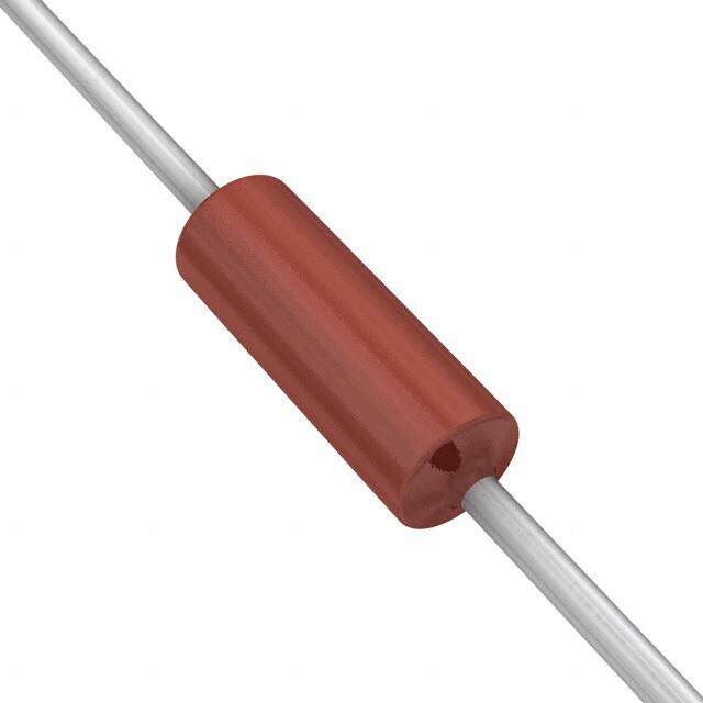
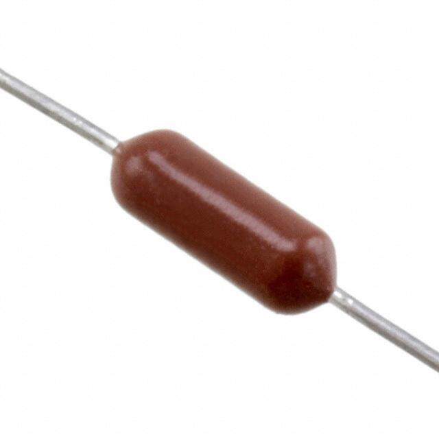
| 描述 | RES 15K OHM 2W 5% AXIAL金属膜电阻器 - 透孔 2watts 15Kohms 5% |
| 产品分类 | |
| 品牌 | Vishay / BC ComponentsVishay BC Components |
| 产品手册 | http://www.vishay.com/doc?28729 |
| 产品图片 |
|
| rohs | 符合RoHS无铅 / 符合限制有害物质指令(RoHS)规范要求 |
| 产品系列 | 薄膜电阻器,金属膜电阻器 - 透孔,Vishay / BC Components PR02000201502JR500PR02 |
| 数据手册 | |
| 产品型号 | PR02000201502JR500PR02000201502JR500 |
| 产品目录绘图 |
|
| 产品种类 | 金属膜电阻器 - 透孔 |
| 供应商器件封装 | 轴向 |
| 其它名称 | BC15KW-2CT |
| 功率(W) | 2W |
| 功率额定值 | 2 W |
| 包装 | 剪切带 (CT) |
| 商标 | Vishay / BC Components |
| 外壳直径 | 3.9 mm |
| 外壳长度 | 10 mm |
| 大小/尺寸 | 0.154" 直径 x 0.394" 长(3.90mm x 10.00mm) |
| 容差 | ±5%5 % |
| 封装 | Reel |
| 封装/外壳 | 轴向 |
| 工作温度范围 | - 55 C to + 175 C |
| 工厂包装数量 | 5000 |
| 引线直径 | 0.78 mm |
| 成分 | 金属薄膜 |
| 标准包装 | 1 |
| 温度系数 | ±250ppm/°C250 PPM / K |
| 特性 | 获得 AEC-Q200 汽车认证, 阻燃涂层 |
| 电压额定值 | 500 V |
| 电阻 | 15 kOhms |
| 电阻(Ω) | 15k |
| 端子数 | 2 |
| 端接类型 | Axial |
| 类型 | High power in small packages |
| 系列 | 5073 |
| 高度 | - |


- 商务部:美国ITC正式对集成电路等产品启动337调查
- 曝三星4nm工艺存在良率问题 高通将骁龙8 Gen1或转产台积电
- 太阳诱电将投资9.5亿元在常州建新厂生产MLCC 预计2023年完工
- 英特尔发布欧洲新工厂建设计划 深化IDM 2.0 战略
- 台积电先进制程称霸业界 有大客户加持明年业绩稳了
- 达到5530亿美元!SIA预计今年全球半导体销售额将创下新高
- 英特尔拟将自动驾驶子公司Mobileye上市 估值或超500亿美元
- 三星加码芯片和SET,合并消费电子和移动部门,撤换高东真等 CEO
- 三星电子宣布重大人事变动 还合并消费电子和移动部门
- 海关总署:前11个月进口集成电路产品价值2.52万亿元 增长14.8%

PDF Datasheet 数据手册内容提取
PR01, PR02, PR03 www.vishay.com Vishay BCcomponents Power Metal Film Leaded Resistors FEATURES • High power in small packages (1 W / 0207 size to 3 W / 0617 size) • Defined fusing characteristics • Technology: metal film • Meets active and passive flammability requirements as defined in IEC 60115-1 • AEC-Q200 qualified (PR01 and PR02) • Material categorization: for definitions of compliance please see www.vishay.com/doc?99912 DESIGN SUPPORT TOOLS click logo to get started APPLICATIONS • All general purpose power applications Models • Automotive electronics Available DESCRIPTION • Lighting ballast A homogeneous film of metal alloy is deposited on a high grade ceramic body. After a helical groove has been cut in the resistive layer, tinned connecting wires of electrolytic copper or copper-clad iron are welded to the end-caps. The resistors are coated with a red, non-flammable lacquer which provides electrical, mechanical and climatic protection. This coating is not resistant to aggressive fluxes and cleaning solvents. The encapsulation is resistant to all cleaning solvents in accordance with IEC 60068-2-45. TECHNICAL SPECIFICATIONS PR02 PR02 PR03 PR03 DESCRIPTION PR01 Cu-lead FeCu-lead Cu-lead FeCu-lead DIN size 0207 0411 0411 0617 0617 Resistance range (1) 0.22 to 1 M 0.33 to 1 M 1 to 1 M 0.68 to 1 M 1 to 1 M Resistance tolerance (2) ± 1 %; ± 5 % ± 1 %; ± 5 % ± 1 %; ± 5 % ± 1 %; ± 5 % ± 1 %; ± 5 % Temperature coefficient ± 250 ppm/K ± 250 ppm/K ± 250 ppm/K ± 250 ppm/K ± 250 ppm/K Rated dissipation, P70 1 R 1 W 2 W 1.3 W 3 W 2.5 W R < 1 0.6 W 1.2 W - 1.6 W - Thermal resistance (R ) 135 K/W 75 K/W 115 K/W 60 K/W 75 K/W th Operating voltage, U AC/DC 350 V 500 V 500 V 750 V 750 V max. E-series E24, E96 (± 1 %); E24 (± 5 %) Basic specification IEC 60115-1 Stability after: Endurance test (1000 h, P70) R max.: ± (5 % R + 0.1 ) Damp heat test (56 days) R max.: ± (3 % R + 0.1 ) Soldering (10 s, 260 °C) R max.: ± (1 % R + 0.05 ) Notes (1) R value is measured with probe distance of 24 mm ± 1 mm using 4-terminal method (2) 1 % tolerance is available for Rn-range from 1 upwards Revision: 11-Jul-2018 1 Document Number: 28729 For technical questions, contact: filmresistorsleaded@vishay.com THIS DOCUMENT IS SUBJECT TO CHANGE WITHOUT NOTICE. THE PRODUCTS DESCRIBED HEREIN AND THIS DOCUMENT ARE SUBJECT TO SPECIFIC DISCLAIMERS, SET FORTH AT www.vishay.com/doc?91000
PR01, PR02, PR03 www.vishay.com Vishay BCcomponents TERMINATION WIRE TYPES PRODUCT TYPE PACKAGING CODE STYLE MATERIAL WIRE DIAMETER PITCH A1, A5, R5 Axial Cu 0.58 mm n/a N4 Radial Cu 0.58 mm 4.8 mm PR01 L1 Radial Cu 0.58 mm 17.8 mm L1 Radial FeCu 0.58 mm 17.8 mm K1 Radial FeCu 0.58 mm 12.5 mm A1, R5 Axial Cu 0.78 mm n/a A1 Axial FeCu 0.58 mm n/a N3, R2 Radial Cu 0.78 mm 4.8 mm PR02 L1 Radial Cu 0.78 mm 17.8 mm L1 Radial FeCu 0.58 mm 17.8 mm B1 Radial FeCu 0.78 mm 15 mm AC Axial Cu 0.78 mm n/a AC Axial FeCu 0.58 mm n/a PR03 DC Radial Cu 0.78 mm 25.4 mm DC Radial FeCu 0.58 mm 25.4 mm PC Radial FeCu 0.78 mm 20 mm APPLICATION INFORMATION The power dissipation on the resistor generates a temperature rise against the local ambient, depending on the heat flow support of the printed-circuit board (thermal resistance). The rated dissipation applies only if the permitted film temperature is not exceeded. Furthermore, a high level of ambient temperature or of power dissipation may raise the temperature of the solder joint, hence special solder alloys or board materials may be required to maintain the reliability of the assembly. These resistors do not feature a limited lifetime when operated within the permissible limits. However, resistance value drift increasing over operating time may result in exceeding a limit acceptable to the specific application, thereby establishing a functional lifetime. The designer may estimate the performance of the particular resistor application or set certain load and temperature limits in order to maintain a desired stability. OPERATION MODE POWER P 70 PR01 1 W Rated dissipation PR02 2 W PR03 3 W Applied maximum film temperature, F max. 250 °C PR01 0.22 to 1 M Max. resistance change at rated PR02 0.33 to 1 M dissipation for resistance range: PR03 0.68 to 1 M |R/R|max. (at P70) after: 1000 h 5.0 % R + 0.1 Revision: 11-Jul-2018 2 Document Number: 28729 For technical questions, contact: filmresistorsleaded@vishay.com THIS DOCUMENT IS SUBJECT TO CHANGE WITHOUT NOTICE. THE PRODUCTS DESCRIBED HEREIN AND THIS DOCUMENT ARE SUBJECT TO SPECIFIC DISCLAIMERS, SET FORTH AT www.vishay.com/doc?91000
PR01, PR02, PR03 www.vishay.com Vishay BCcomponents PART NUMBER AND PRODUCT DESCRIPTION Part Number: PR02000201001JA100 P R 0 2 0 0 0 2 0 1 0 0 1 J A 1 0 0 TYPE/SIZE VARIANT WIRE TYPES TCR/MATERIAL RESISTANCE TOLERANCE PACKAGING SPECIAL PR0100 0 = neutral 1 = Cu 0.58 0 = standard 3 digit value F = ± 1 % N4 R2 00 = PR0200 Z = value (PR01) 1 digit multiplier J = ± 5 % N3 L1 standard PR0300 overflow 2 = Cu 0.78 Multiplier A5 DC (special) (PR02, PR03) 7 = *10-3 A1 K1 AC B1 3 = FeCu 0.58 8 = *10-2 R5 PC (PR01, PR02, 9 = *10-1 PR03) 0 = *100 4 = FeCu 0.78 1 = *101 (PR02, PR03) 2 = *102 3 = *103 4 = *104 Product Description: PR02 5 % A1 1K0 PR02 5 % A1 1K0 TYPE TOLERANCE PACKAGING RESISTANCE VALUE PR01 1 % N4 R2 1K0 = 1 k PR02 5 % N3 L1 4K75 = 4.75 k A5 DC PR03 A1 K1 AC B1 R5 PC Note • The products can be ordered using either the PRODUCT DESCRIPTION or the PART NUMBER PACKAGING PRODUCT TAPE CODE QUANTITY DESCRIPTION PITCH DIMENSION TYPE WIDTH A5 5000 Ammo pack acc. to IEC 60286-1 5 mm 52 mm 75 mm x 114 mm x 260 mm A1 1000 Ammo pack acc. to IEC 60286-1 5 mm 52 mm 78 mm x 31 mm x 260 mm N4 4000 Ammo pack acc. to IEC 60286-2 - - 45 mm x 262 mm x 330 mm PR01 L1 1000 Loose in bulk - - 105 mm x 70 mm x 205 mm K1 1000 Loose in bulk - - 105 mm x 70 mm x 205 mm R5 5000 Reel pack acc. to IEC 60286-1 5 mm 52 mm 93 mm x 300 mm x 298 mm A1 1000 Ammo pack acc. to IEC 60286-1 5 mm 52 mm 72 mm x 60 mm x 258 mm N3 3000 Ammo pack acc. to IEC 60286-2 - - 45 mm x 262 mm x 330 mm L1 1000 Loose in bulk - - 105 mm x 70 mm x 205 mm PR02 B1 1000 Loose in bulk - - 105 mm x 70 mm x 205 mm R5 5000 Reel pack acc. to IEC 60286-1 5 mm 52 mm 100 mm x 375 mm x 375 mm R2 2000 Reel pack acc. to IEC 60286-2 - - 90 mm x 375 mm x 375 mm AC 500 Ammo pack acc. to IEC 60286-1 10 mm 63 mm 83 mm x 58 mm x 256 mm PR03 DC 500 Loose in bulk - - 105 mm x 70 mm x 205 mm PC 500 Loose in bulk - - 105 mm x 70 mm x 205 mm Revision: 11-Jul-2018 3 Document Number: 28729 For technical questions, contact: filmresistorsleaded@vishay.com THIS DOCUMENT IS SUBJECT TO CHANGE WITHOUT NOTICE. THE PRODUCTS DESCRIBED HEREIN AND THIS DOCUMENT ARE SUBJECT TO SPECIFIC DISCLAIMERS, SET FORTH AT www.vishay.com/doc?91000
PR01, PR02, PR03 www.vishay.com Vishay BCcomponents DESCRIPTION ASSEMBLY Production is strictly controlled and follows an extensive The resistors are suitable for processing on automatic set of instructions established for reproducibility. A insertion equipment and cutting and bending machines. homogeneous film of metal alloy is deposited on a high Excellent solderability is proven, even after extended grade ceramic body and conditioned to achieve the desired storage. They are suitable for automatic soldering using temperature coefficient. Plated steel termination caps are wave or dipping. firmly pressed on the metalized rods. Mostly, a special laser The resistors are completely lead (Pb)-free, the pure tin is used to achieve the target value by smoothly cutting a plating provides compatibility with lead (Pb)-free and helical groove in the resistive layer without damaging the lead-containing soldering processes. The immunity of the ceramics. Connecting wires of electrolytic copper plated plating against tin whisker growth, in compliance with with 100 % pure tin are welded to the termination caps. IEC 60068-2-82, has been proven under extensive testing. The resistor elements are covered by a red, non-flammable The encapsulant is resistant to cleaning solvent specified in lacquer protective coating designed for electrical, IEC 60115-1. The suitability of conformal coatings, if mechanical, and climatic protection. Four or five color code applied, shall be qualified by appropriate means to ensure rings designate the resistance value and tolerance in the long-term stability of the whole system. accordance with IEC 60062. The result of the determined production is verified by an RELATED PRODUCTS extensive testing procedure performed on 100 % of the For a correlated range of Metal Film Resistors see the individual resistors. Only accepted products are stuck datasheet: directly on the adhesive tapes in accordance with IEC 60286-1 or for the radial versions in accordance to “High Ohmic / High Voltage Metal Film Leaded Resistors”, IEC 60286-2. www.vishay.com/doc?30260 For product that offers high power dissipation and metal MATERIALS oxide film technology see the datasheet: Vishay acknowledges the following systems for the “High Power Metal Oxide Leaded Resistors”, regulation of hazardous substances: www.vishay.com/doc?20128 • IEC 62474, Material Declaration for Products of and for the Electrotechnical Industry, with the list of declarable substances given therein (1) • The Global Automotive Declarable Substance List (GADSL) (2) • The REACH regulation (1907/2006/EC) and the related list of substances with very high concern (SVHC) (3) for its supply chain The products do not contain any of the banned substances as per IEC 62474, GADSL, or the SVHC list, see www.vishay.com/how/leadfree. Hence the products fully comply with the following directives: • 2000/53/EC End-of-Life Vehicle Directive (ELV) and Annex II (ELV II) • 2011/65/EU Restriction of the Use of Hazardous Substances Directive (RoHS) with amendment 2015/863/EU • 2012/19/EU Waste Electrical and Electronic Equipment Directive (WEEE) Vishay pursues the elimination of conflict minerals from its supply chain, see the Conflict Minerals Policy at www.vishay.com/doc?49037. Notes (1) The IEC 62474 list of declarable substances is maintained in a dedicated database, which is available at http://std.iec.ch/iec62474 (2) The Global Automotive Declarable Substance List (GADSL) is maintained by the American Chemistry Council, and available at www.gadsl.org (3) The SVHC list is maintained by the European Chemical Agency (ECHA) and available at http://echa.europa.eu/candidate-list-table Revision: 11-Jul-2018 4 Document Number: 28729 For technical questions, contact: filmresistorsleaded@vishay.com THIS DOCUMENT IS SUBJECT TO CHANGE WITHOUT NOTICE. THE PRODUCTS DESCRIBED HEREIN AND THIS DOCUMENT ARE SUBJECT TO SPECIFIC DISCLAIMERS, SET FORTH AT www.vishay.com/doc?91000
PR01, PR02, PR03 www.vishay.com Vishay BCcomponents FUNCTIONAL PERFORMANCE The power that the resistor can dissipate depends on the operating temperature. 100 % n r i e 80 w o P 60 40 20 0 -55 0 50 70 100 150 200 Ambient Temperature in °C Derating Maximum dissipation (P ) in percentage of rated power as a function of the ambient temperature (T ) max. amb 50 50 Δ T ΔT (K) 15 mm (K) 15 mm 40 40 20 mm 20 mm 30 30 20 20 10 10 0 0 0 0.4 0.8 P (W) 1.2 0 0.4 0.8 P (W) 1.2 Ø 0.58 mm Cu-leads Ø 0.58 mm FeCu-leads Minimum distance from resistor body to PCB = 1 mm Minimum distance from resistor body to PCB = 1 mm PR01 Temperature rise (T) at the lead end (soldering point) as a PR01 Temperature rise (T) at the lead end (soldering point) as a function of dissipated power at various lead lengths after mounting. function of dissipated power at various lead lengths after mounting. 70 100 Δ T Δ T (K) 15 mm (K) 60 80 15 mm 50 20 mm 60 40 20 mm 30 40 20 20 10 0 0 0 1 P (W) 2 0 1 P (W) 2 Ø 0.58 mm FeCu-leads Ø 0.78 mm Cu-leads Minimum distance from resistor body to PCB = 1 mm Minimum distance from resistor body to PCB = 1 mm PR02 Temperature rise (T) at the lead end (soldering point) as a PR02 Temperature rise (T) at the lead end (soldering point) as a function of dissipated power at various lead lengths after mounting. function of dissipated power at various lead lengths after mounting. Revision: 11-Jul-2018 5 Document Number: 28729 For technical questions, contact: filmresistorsleaded@vishay.com THIS DOCUMENT IS SUBJECT TO CHANGE WITHOUT NOTICE. THE PRODUCTS DESCRIBED HEREIN AND THIS DOCUMENT ARE SUBJECT TO SPECIFIC DISCLAIMERS, SET FORTH AT www.vishay.com/doc?91000
PR01, PR02, PR03 www.vishay.com Vishay BCcomponents 80 100 ΔT ΔT (K) (K) 15 mm 15 mm 80 20 mm 60 20 mm 60 40 40 20 20 0 0 0 0.2 0.4 0.6 0.8 1.0 1.2 1.4 1.6 1.8 2.0 2.2 0 1 2 P (W) 3 Ø 0.78 mm FeCu-leads P (W) Ø 0.78 mm Cu-leads Minimum distance from resistor body to PCB = 1 mm Minimum distance from resistor body to PCB = 1 mm PR02 Temperature rise (T) at the lead end (soldering point) as a PR03 Temperature rise (T) at the lead end (soldering point) as a function of dissipated power at various lead lengths after mounting. function of dissipated power at various lead lengths after mounting. 80 80 Δ T 10 mm ΔT (K) (K) 15 mm 60 60 15 mm 20 mm 20 mm 40 40 20 20 0 0 0 1 2 P (W) 3 0 0.8 1.6 2.4 P (W)3.2 Ø 0.58 mm FeCu-leads Ø 0.78 mm FeCu-leads Minimum distance from resistor body to PCB = 1 mm Minimum distance from resistor body to PCB = 1 mm PR03 Temperature rise (T) at the lead end (soldering point) as a PR03 Temperature rise (T) at the lead end (soldering point) as a function of dissipated power at various lead lengths after mounting. function of dissipated power at various lead lengths after mounting. Revision: 11-Jul-2018 6 Document Number: 28729 For technical questions, contact: filmresistorsleaded@vishay.com THIS DOCUMENT IS SUBJECT TO CHANGE WITHOUT NOTICE. THE PRODUCTS DESCRIBED HEREIN AND THIS DOCUMENT ARE SUBJECT TO SPECIFIC DISCLAIMERS, SET FORTH AT www.vishay.com/doc?91000
PR01, PR02, PR03 www.vishay.com Vishay BCcomponents ΔT ΔT (K) (K) 120 120 80 80 40 40 0 0 0 0.2 0.4 0.6 0.8 1.0 0 0.2 0.4 0.6 0.8 P (W) P (W) Ø 0.58 mm Cu-leads Ø 0.58 mm FeCu-leads PR01 Hot-spot temperature rise (T) as a function PR01 Hot-spot temperature rise (T) as a function of dissipated power. of dissipated power. 160 160 Δ T ΔT (K) (K) 120 120 80 80 40 40 0 0 0 0.4 0.8 1.2 1.6 2.0 0 0.2 0.4 0.6 0.8 1.0 1.2 1.4 P (W) P (W) Ø 0.78 mm Cu-leads Ø 0.78 mm FeCu-leads PR02 Hot-spot temperature rise (T) as a function PR02 Hot-spot temperature rise (T) as a function of dissipated power. of dissipated power. 160 200 Δ T Δ T (K) (K) 160 120 120 80 80 40 40 0 0 0 0.2 0.4 0.6 0.8 1.0 1.2 1.4 0 1 2 P (W) P (W) Ø 0.58 mm FeCu-leads Ø 0.58 mm FeCu-leads PR02 Hot-spot temperature rise (T) as a function PR03 Hot-spot temperature rise (T) as a function of dissipated power. of dissipated power. Revision: 11-Jul-2018 7 Document Number: 28729 For technical questions, contact: filmresistorsleaded@vishay.com THIS DOCUMENT IS SUBJECT TO CHANGE WITHOUT NOTICE. THE PRODUCTS DESCRIBED HEREIN AND THIS DOCUMENT ARE SUBJECT TO SPECIFIC DISCLAIMERS, SET FORTH AT www.vishay.com/doc?91000
PR01, PR02, PR03 www.vishay.com Vishay BCcomponents 200 200 ∆ T ΔT (K) (K) 160 160 120 120 80 80 40 40 0 0 0 1 2 P (W) 3 0 1 2 P (W) Ø 0.78 mm Cu-leads Ø 0.78 mm FeCu-leads PR03 Hot-spot temperature rise (T) as a function PR03 Hot-spot temperature rise (T) as a function of dissipated power. of dissipated power. Revision: 11-Jul-2018 8 Document Number: 28729 For technical questions, contact: filmresistorsleaded@vishay.com THIS DOCUMENT IS SUBJECT TO CHANGE WITHOUT NOTICE. THE PRODUCTS DESCRIBED HEREIN AND THIS DOCUMENT ARE SUBJECT TO SPECIFIC DISCLAIMERS, SET FORTH AT www.vishay.com/doc?91000
PR01, PR02, PR03 www.vishay.com Vishay BCcomponents The maximum permissible hot-spot temperature is 205 °C for PR01, 220 °C for PR02 and 250 °C for PR03. 1.00 Tamb = 40 °C 70 °C P (W) 100 °C 0.75 125 °C 0.50 155 °C 0.25 205 °C Tm (°C) 100 100 000 00h1 0h00 h > 3<0 <3 k0 1 Ωk k ΩΩ 10 5.0 2.0 1.0 0.5 0.2 0.1 % ΔR PR01 Drift nomogram 2.00 Tamb = 40 °C 7 0 °C P (W) 1.50 100 °C 125 °C 1.00 155 °C 0.50 220 °C 100 0100 0 01h000 0h0 h > <3 93< 9 k1 Ωk k ΩΩ Tm (°C) 10 5.0 2.0 1.0 0.5 0.2 0.1 % ΔR PR02 Drift nomogram 3.00 Tamb = 4 0 °C 7 0 °C P (W) 100 °C 2.25 125 °C 155 °C 1.50 0.75 2 50 °C 1010 0 01000000 00 h hh > 5≤ 15< 1 k1 Ωk kΩΩ Tm (°C) 10 5.0 2.0 1.0 0.5 0.2 0.1 % ΔR PR03 Drift nomogram Revision: 11-Jul-2018 9 Document Number: 28729 For technical questions, contact: filmresistorsleaded@vishay.com THIS DOCUMENT IS SUBJECT TO CHANGE WITHOUT NOTICE. THE PRODUCTS DESCRIBED HEREIN AND THIS DOCUMENT ARE SUBJECT TO SPECIFIC DISCLAIMERS, SET FORTH AT www.vishay.com/doc?91000
PR01, PR02, PR03 www.vishay.com Vishay BCcomponents 103 Pmax. (W) tp/ti = 1000 500 102 200 100 50 20 10 10 5 2 1 10-1 10-6 10-5 10-4 10-3 10-2 10-1 1 t(s) i ˆ PR01 Pulse on a regular basis; maximum permissible peak pulse power (P ) as a function of pulse duration (t) max. i 1200 Umax. (V) 1000 800 600 400 200 0 10-6 10-5 10-4 10-3 10-2 10-1 t(s) 1 i PR01 Pulse on a regular basis; maximum permissible peak pulse voltage (Û ) as a function of pulse duration (t) max. i 103 P max. (W) tp/ t i = 1005000 102 200 100 50 20 10 10 5 2 1 10-1 10-6 10-5 10-4 10-3 10-2 10-1 ti(s) 1 ˆ PR02 Pulse on a regular basis; maximum permissible peak pulse power (P ) as a function of pulse duration (t) max. i Revision: 11-Jul-2018 10 Document Number: 28729 For technical questions, contact: filmresistorsleaded@vishay.com THIS DOCUMENT IS SUBJECT TO CHANGE WITHOUT NOTICE. THE PRODUCTS DESCRIBED HEREIN AND THIS DOCUMENT ARE SUBJECT TO SPECIFIC DISCLAIMERS, SET FORTH AT www.vishay.com/doc?91000
PR01, PR02, PR03 www.vishay.com Vishay BCcomponents 1700 Umax. (V) 1500 1300 1100 900 700 500 10-6 10-5 10-4 10-3 10-2 10-1 1 t(s) i PR02 Pulse on a regular basis; maximum permissible peak pulse voltage (Û ) as a function of pulse duration (t) max. i 104 P max. (W) 103 t/t = 1000 p i 500200 100 102 50 20 10 5 10 2 1 10-6 10-5 10-4 10-3 10-2 10-1 1 t(s) i ˆ PR03 Pulse on a regular basis; maximum permissible peak pulse power (P ) as a function of pulse duration (t) max. i 2400 Umax. (V) 2000 1600 1200 800 400 0 10-6 10-5 10-4 10-3 10-2 10-1 1 t(s) i PR03 Pulse on a regular basis; maximum permissible peak pulse voltage (Û ) as a function of pulse duration (t) max. i Revision: 11-Jul-2018 11 Document Number: 28729 For technical questions, contact: filmresistorsleaded@vishay.com THIS DOCUMENT IS SUBJECT TO CHANGE WITHOUT NOTICE. THE PRODUCTS DESCRIBED HEREIN AND THIS DOCUMENT ARE SUBJECT TO SPECIFIC DISCLAIMERS, SET FORTH AT www.vishay.com/doc?91000
PR01, PR02, PR03 www.vishay.com Vishay BCcomponents 102 10 2 t t (s) (s) 10 10 1 1 10-1 10-1 0 10 20 30 Pover4lo0ad(W) 50 0 10 20 30 Pover4lo0a d (W)50 PR01 Time to interruption as a function of overload power PR01 Time to interruption as a function of overload power for range: 0.22 Rn 1 for range: 16 Rn 560 This graph is based on measured data under constant voltage This graph is based on measured data under constant voltage conditions; the data may deviate according to the applications. conditions; the data may deviate according to the applications. 10 2 10 2 t t (s) (s) 10 10 1 1 10 - 1 10-1 0 10 20 30 40 50 0 20 40 60 80 100 120 P (W) P (W) overload overload PR01 Time to interruption as a function of overload power PR02 Time to interruption as a function of overload power for range: 1 Rn 15 for range: 0.33 Rn 5 This graph is based on measured data under constant voltage This graph is based on measured data under constant voltage conditions; the data may deviate according to the applications. conditions; the data may deviate according to the applications. 10 2 10 2 t t (s) (s) 10 10 1 1 10-1 10-1 0 20 40 60 80 100 120 0 20 40 60 80 100 120 P (W) P (W) overload overload PR02 Time to interruption as a function of overload power PR02 Time to interruption as a function of overload power for range: 5 Rn 68 for range: 68 Rn 560 This graph is based on measured data under constant voltage This graph is based on measured data under constant voltage conditions; the data may deviate according to the applications. conditions; the data may deviate according to the applications. Revision: 11-Jul-2018 12 Document Number: 28729 For technical questions, contact: filmresistorsleaded@vishay.com THIS DOCUMENT IS SUBJECT TO CHANGE WITHOUT NOTICE. THE PRODUCTS DESCRIBED HEREIN AND THIS DOCUMENT ARE SUBJECT TO SPECIFIC DISCLAIMERS, SET FORTH AT www.vishay.com/doc?91000
PR01, PR02, PR03 www.vishay.com Vishay BCcomponents 10 2 t (s) 10 1 10-1 0 50 100 150 200 250 P (W) overload PR03 Time to interruption as a function of overload power for range: 0.68 Rn 560 This graph is based on measured data under constant voltage conditions; the data may deviate according to the applications. Revision: 11-Jul-2018 13 Document Number: 28729 For technical questions, contact: filmresistorsleaded@vishay.com THIS DOCUMENT IS SUBJECT TO CHANGE WITHOUT NOTICE. THE PRODUCTS DESCRIBED HEREIN AND THIS DOCUMENT ARE SUBJECT TO SPECIFIC DISCLAIMERS, SET FORTH AT www.vishay.com/doc?91000
PR01, PR02, PR03 www.vishay.com Vishay BCcomponents 10 2 Z R R n = 1 Ω 10 R n = 24 Ω 1 R n = 12 kΩ 10 -1 R n = 100 kΩ 10 -2 10-1 1 10 10 2 f (MHz) 10 3 PR01 Impedance as a function of applied frequency 10 2 Z R R n = 1.2 Ω 10 R n = 10 Ω 1 R n = 22 kΩ 10 -1 R n = 124 kΩ 10 -2 10 -1 1 10 10 2 f (MHz) 10 3 PR02 Impedance as a function of applied frequency 10 2 Z R R n = 1.5 Ω 10 R n = 18 Ω 1 R n = 1.3 kΩ 10-1 R n = 20 kΩ R n = 100 kΩ 10-2 1 10 102 f (MHz) 103 PR03 Impedance as a function of applied frequency Revision: 11-Jul-2018 14 Document Number: 28729 For technical questions, contact: filmresistorsleaded@vishay.com THIS DOCUMENT IS SUBJECT TO CHANGE WITHOUT NOTICE. THE PRODUCTS DESCRIBED HEREIN AND THIS DOCUMENT ARE SUBJECT TO SPECIFIC DISCLAIMERS, SET FORTH AT www.vishay.com/doc?91000
PR01, PR02, PR03 www.vishay.com Vishay BCcomponents TESTS PROCEDURES AND REQUIREMENTS All tests are carried out in accordance with the following Unless otherwise specified the following values apply: specifications: • Temperature: 15 °C to 35 °C • IEC 60115-1, generic specification (includes tests) • Relative humidity: 45 % to 75 % The test and requirements table contains only the most • Air pressure: 86 kPa to 106 kPa (860 mbar to 1060 mbar). important tests. For the full test schedule refer to the documents listed above. For performing some of the tests, the components are mounted on a test board in accordance with IEC 60115-1, The tests are carried out in accordance with IEC 60068-2-xx 4.31. test method and under standard atmospheric conditions in accordance with IEC 60068-1, 5.3. In test procedures and requirements table, only the tests and requirements are listed with reference to the relevant Climatic category LCT / UCT / 56 (rated temperature range: clauses of IEC 60115-1 and IEC 60068-2-xx test methods. lower category temperature, upper category temperature; A short description of the test procedure is also given. damp heat, steady state, test duration: 56 days) is valid. TEST PROCEDURES AND REQUIREMENTS IEC IEC REQUIREMENTS PERMISSIBLE 60068-2- 60115-1 TEST PROCEDURE CHANGE TEST CLAUSE METHOD (Rmax.) 4.4.1 - Visual examination No holes; clean surface; no damage See Straight and Kinked Dimensions 4.4.2 - Dimensions (outline) Gauge (mm) tables 4.5 - Resistance ± 5 % R Maximum voltage (DC) after 1 min; 4.6.1.1 - Insulation resistance metal block method Rins min.: 104 M 4.7 - Voltage proof U = U ; 60 s No breakdown or flashover RMS ins Temperature At (20 / -55 / 20) °C 4.8 - ± 250 ppm/K coefficient and (20 / 155 / 20) °C 21 (Ua ) 1 Robustness of No damage 4.16 21 (Ub) Tensile, bending, and torsion 21 (Uc) terminations Rmax.: ± (0.5 % R + 0.05 ) +235 °C; 2 s; Good tinning solder bath method; SnPb40 ( 95 % covered, no visible damage) 4.17 20 (Ta) Solderability +245 °C; 3 s; Good tinning solder bath method; SnAg3Cu0.5 ( 95 % covered, no visible damage) Resistance to Unmounted components 4.18.2 20 (Tb) soldering heat (260 ± 5) °C; (10 ± 1) s Rmax.: ± (1 % R + 0.05 ) No visual damage 4.19 14 (Na) Rapid change of 30 min at -55 °C and PR01: Rmax.: ± (1 % R + 0.05 ) temperature 30 min at +200 °C; 5 cycles PR02: Rmax.: ± (1 % R + 0.05 ) PR03: Rmax.: ± (2 % R + 0.05 ) No damage 4.20 29 (Eb) Bump 3 x 1500 bumps in three directions; 40 g Rmax.: ± (0.5 % R + 0.05 ) 10 sweep cycles per direction; No damage 4.22 6 (Fc) Vibration 10 Hz to 2000 Hz; 1.5 mm or 200 m/s2 Rmax.: ± (0.5 % R + 0.05 ) Revision: 11-Jul-2018 15 Document Number: 28729 For technical questions, contact: filmresistorsleaded@vishay.com THIS DOCUMENT IS SUBJECT TO CHANGE WITHOUT NOTICE. THE PRODUCTS DESCRIBED HEREIN AND THIS DOCUMENT ARE SUBJECT TO SPECIFIC DISCLAIMERS, SET FORTH AT www.vishay.com/doc?91000
PR01, PR02, PR03 www.vishay.com Vishay BCcomponents TEST PROCEDURES AND REQUIREMENTS IEC IEC REQUIREMENTS PERMISSIBLE 60068-2- 60115-1 TEST PROCEDURE CHANGE TEST CLAUSE METHOD (Rmax.) 4.23 Climatic sequence: 4.23.2 2 (Ba) Dry heat 200 °C; 16 h Damp heat, 55 °C; 24 h; 4.23.3 30 (Db) cyclic 90 % to 100 % RH; 1 cycle 4.23.4 1 (Aa) Cold -55 °C; 2 h Rins min.: 103 M Rmax.: ± (1.5 % R + 0.1 ) 8.5 kPa; 2 h; 4.23.5 13 (M) Low air pressure 15 °C to 35 °C Damp heat, 55 °C; 5 days; 4.23.6 30 (Db) cyclic 95 % to 100 % RH; 5 cycles Damp heat (40 ± 2) °C; 56 days; 4.24 78 (Cab) (steady state) (93 ± 3 )% RH Rmax.: ± (3 % R + 0.1 ) Endurance U = P x R or U = U ; 4.25.1 - (at 70 °C) 1.5 h on; 07.05 h off; 70 °C; 1m0ax0.0 h Rmax.: ± (5 % R + 0.1 ) No damage, 4.26 - Active flammability Accidental overload test no flamming of gauze cylinder Component solvent Isopropyl alcohol (used in industrial application) 4.29 45 (Xa) Marking legible; no visible damage resistance +23 °C; toothbrush method No ignition of product, 4.35 - Passive flammability Needle flame test no ignition of under layer burning time is less than 30 s Revision: 11-Jul-2018 16 Document Number: 28729 For technical questions, contact: filmresistorsleaded@vishay.com THIS DOCUMENT IS SUBJECT TO CHANGE WITHOUT NOTICE. THE PRODUCTS DESCRIBED HEREIN AND THIS DOCUMENT ARE SUBJECT TO SPECIFIC DISCLAIMERS, SET FORTH AT www.vishay.com/doc?91000
PR01, PR02, PR03 www.vishay.com Vishay BCcomponents DIMENSIONS D d L 1 L 2 Type with straight leads DIMENSIONS - Straight lead type and relevant physical dimensions; see straight leads outline TERMINATION WIRE MATERIAL (Cu OR FeCu) Ø D L L AND WIRE DIAMETER (Ø d) MASS TYPE MAX. 1 MAX. 2 MAX. (mm) (mm) (mm) Ø d (mg) MATERIAL (mm) Cu 0.58 ± 0.05 212 PR01 2.5 6.5 8.0 FeCu 0.58 ± 0.05 207 Cu 0.78 ± 0.05 504 PR02 3.9 10.0 12.0 FeCu 0.58 ± 0.05 455 FeCu 0.78 ± 0.05 496 Cu 0.78 ± 0.05 1192 PR03 5.2 16.7 19.5 FeCu 0.58 ± 0.05 1079 FeCu 0.78 ± 0.05 1185 P1 ± 0.5 Ø D P1 ± 0.5 8 + 2 L 1 L2 4.5 + 10 Ø d b P ± 3 S Ø B b1 2 ± 0.07 2 Type with double kink Dimensions in millimeters DIMENSIONS - Double kink lead type and relevant physical dimensions; see double kinked outline TERMINATION WIRE MATERIAL Ø D L L (Cu OR FeCu) AND MASS PITCH P P b b S Ø B TYPE (mMmA)X. (1m MmAX). (2m MmAX). WIRE DIAMETER (Ø d) (mg) (mm) (mm1) (mm2) (mm1 ) (mm2 ) (mMmAX). (mm) Ø d MATERIAL (mm) 0.58 17.8 17.8 1.10 1.45 0.8 Cu 212 17.8 2 ± 0.05 ± 0.5 ± 3 + 0.25 / - 0.20 + 0.25 / - 0.20 ± 0.07 0.58 12.5 12.5 1.10 1.45 0.8 PR01 2.5 6.5 8.0 FeCu 207 12.5 2 ± 0.05 ± 0.5 ± 3 + 0.25 / - 0.20 + 0.25 / - 0.20 ± 0.07 0.58 17.8 17.8 1.10 1.45 0.8 FeCu 207 17.8 2 ± 0.05 ± 0.5 ± 3 + 0.25 / - 0.20 + 0.25 / - 0.20 ± 0.07 0.78 17.8 17.8 1.10 1.45 1.0 Cu 504 17.8 2 ± 0.05 ± 0.5 ± 3 + 0.25 / - 0.20 + 0.25 / - 0.20 ± 0.07 0.58 17.8 17.8 1.10 1.45 0.8 PR02 3.9 10.0 12.0 FeCu 455 17.8 2 ± 0.05 ± 0.5 ± 3 + 0.25 / - 0.20 + 0.25 / - 0.20 ± 0.07 0.78 15.0 15.0 1.30 1.65 1.0 FeCu 496 15.0 2 ± 0.05 ± 0.5 ± 3 + 0.25 / - 0.20 + 0.25 / - 0.20 ± 0.07 0.78 25.4 25.4 1.10 1.65 1.0 Cu 1192 25.4 2 ± 0.05 ± 0.5 ± 3 + 0.25 / - 0.20 + 0.25 / - 0.20 ± 0.07 0.58 25.4 25.4 1.10 1.65 1.0 PR03 5.2 16.7 FeCu 1079 25.4 2 19.5 ± 0.05 ± 0.5 ± 3 + 0.25 / - 0.20 + 0.25 / - 0.20 ± 0.07 0.78 22.0 20.0 1.30 2.15 1.0 FeCu 1185 20 2 ± 0.05 ± 0.5 ± 3 + 0.25 / - 0.20 + 0.25 / - 0.20 ± 0.07 Revision: 11-Jul-2018 17 Document Number: 28729 For technical questions, contact: filmresistorsleaded@vishay.com THIS DOCUMENT IS SUBJECT TO CHANGE WITHOUT NOTICE. THE PRODUCTS DESCRIBED HEREIN AND THIS DOCUMENT ARE SUBJECT TO SPECIFIC DISCLAIMERS, SET FORTH AT www.vishay.com/doc?91000
PR01, PR02, PR03 www.vishay.com Vishay BCcomponents PR01, PR02 WITH RADIAL TAPING PR01 - Height for insertion (max.) = 32 mm DIMENSIONS in millimeters Pitch of components P 12.7 ± 1.0 P2 P Feed-hole pitch P 12.7 ± 0.2 0 Feed-hole centre to lead P 3.85 ± 0.5 at topside at the tape 1 Feed-hole center to body center P 6.35 ± 1.0 2 H Lead spacing F 4.8 +0.7/-0 1 Width of carrier tape W 18.0 ± 0.5 H H0LL1 W Minimum hold down tape width W0 5.5 0 Height for insertion (max.) H1 32 W Lead wire clinch height H 16.5 ± 0.5 0 Body to hole center H 19.5 ± 1 Feed-hole diameter D 4.0 ± 0.2 0 α α F P0 P1 D0 Height for cutting (max.) L 11.0 Minimum lead wire (tape portion) α = 30° to 40° shortest lead L1 2.5 a a PR02 - Height for insertion (max.) = 29 mm DIMENSIONS in millimeters Pitch of components P 12.7 ± 1.0 P2 P Feed-hole pitch P 12.7 ± 0.2 0 Feed-hole centre to lead P 3.85 ± 0.5 at topside at the tape 1 Feed-hole center to body center P 6.35 ± 1.0 2 H Lead spacing F 4.8 +0.7/-0 1 Width of carrier tape W 18.0 ± 0.5 H H0LL1 W Minimum hold down tape width W0 5.5 0 Height for insertion (max.) H1 29 W Lead wire clinch height H 16.5 ± 0.5 0 Body to hole center H 19.5 ± 1 Feed-hole diameter D 4.0 ± 0.2 0 α α F P0 P1 D0 Height for cutting (max.) L 11.0 Minimum lead wire (tape portion) α = 30° to 40° shortest lead L1 2.5 a a MARKING The nominal resistance and tolerance are marked on the resistor using four or five colored bands in accordance with IEC 60062, marking codes for resistors and capacitors. Revision: 11-Jul-2018 18 Document Number: 28729 For technical questions, contact: filmresistorsleaded@vishay.com THIS DOCUMENT IS SUBJECT TO CHANGE WITHOUT NOTICE. THE PRODUCTS DESCRIBED HEREIN AND THIS DOCUMENT ARE SUBJECT TO SPECIFIC DISCLAIMERS, SET FORTH AT www.vishay.com/doc?91000
PR01, PR02, PR03 www.vishay.com Vishay BCcomponents 12NC INFORMATION FOR HISTORICAL CODING REFERENCE The resistors have a 12-digit numeric code starting with 23 Last Digit of 12NC Indicating Resistance Decade For 5 % tolerance: RESISTANCE DECADE LAST DIGIT • The next 7 digits indicate the resistor type and packing 0.22 to 0.91 7 • The remaining 3 digits indicate the resistance value: 1 to 9.76 8 - The first 2 digits indicate the resistance value 10 to 97.6 9 - The last digit indicates the resistance decade 100 to 976 1 For 1 % tolerance: 1 to 9.76 k 2 10 to 97.6 k 3 • The next 6 digits indicate the resistor type and packing 100 to 976 k 4 • The remaining 4 digits indicate the resistance value: 1 M 5 - The first 3 digits indicate the resistance value 12NC Example - The last digit indicates the resistance decade The 12NC for resistor type PR02 with Cu leads and a value of 750 with 5 % tolerance, supplied on a bandolier of 1000 units in ammopack, is: 2306 198 53751. 12NC - Resistor Type and Packaging (1) 23.. ... ..... (BANDOLIER) AMMOPACK REEL LEAD Ø TOL. TYPE STRAIGHT LEADS mm (%) RADIAL TAPED RADIAL TAPED 52 mm 52 mm 63 mm 52 mm 4000 UNITS 3000 UNITS 5000 UNITS 1000 UNITS 500 UNITS 5000 UNITS 2000 UNITS 1 - - 22 196 1.... 06 191 2.... - 06 191 5.... - PR01 Cu 0.58 5 06 197 03... - 22 193 14... 06 197 53... - 06 197 23... - 1 - 22 197 2.... - 22 197 1.... - - 2322 197 5.... Cu 0.78 PR02 5 - 06 198 03... - 06 198 53... - - 2322 198 04... FeCu 0.58 5 - - - 22 194 54... - - - 5 - - - - 22 195 14... - - Cu 0.78 PR03 1 - - - - 06 199 6... - - FeCu 0.58 5 - - - - 22 195 54... - - Notes • Preferred types in bold (1) Other packaging versions are available on request 12NC - Resistor Type and Packaging 23.. ... ..... (LOOSE IN BOX) LEAD Ø TOL. DOUBLE KINK TYPE mm (%) PITCH = 17.8 mm PITCH = 25.4 mm PITCH (2)(3)(4) 1000 UNITS 500 UNITS 1000 UNITS 500 UNITS Cu 0.58 5 22 193 03... - - - PR01 FeCu 0.58 5 22 193 43... - 22 193 53... (2) - Cu 0.78 5 22 194 23... - - - PR02 FeCu 0.58 5 22 194 83... - - - FeCu 0.78 5 - - 22 194 63... (3) - Cu 0.78 5 - 22 195 23... - - PR03 FeCu 0.58 5 - 22 195 83... - - FeCu 0.78 5 - - - 22 195 63... (4) Notes • Preferred types in bold (2) PR01 pitch 12.5 mm (3) PR02 pitch 15.0 mm (4) PR03 pitch 20.0 mm, with reversed kinking direction as opposed to the drawing for the type with double kink figure Revision: 11-Jul-2018 19 Document Number: 28729 For technical questions, contact: filmresistorsleaded@vishay.com THIS DOCUMENT IS SUBJECT TO CHANGE WITHOUT NOTICE. THE PRODUCTS DESCRIBED HEREIN AND THIS DOCUMENT ARE SUBJECT TO SPECIFIC DISCLAIMERS, SET FORTH AT www.vishay.com/doc?91000
Legal Disclaimer Notice www.vishay.com Vishay Disclaimer ALL PRODUCT, PRODUCT SPECIFICATIONS AND DATA ARE SUBJECT TO CHANGE WITHOUT NOTICE TO IMPROV E RELIABILITY, FUNCTION OR DESIGN OR OTHERWISE. Vishay Intertechnology, Inc., its affiliates, agents, and employees, and all persons acting on its or their behalf (collectively, “Vishay”), disclaim any and all liability for any errors, inaccuracies or incompleteness contained in any datasheet or in any other disclosure relating to any product. Vishay makes no warranty, representation or guarantee regarding the suitability of the products for any particular purpose o r the continuing production of any product. To the maximum extent permitted by applicable law, Vishay disclaims (i) any and all liability arising out of the application or use of any product, (ii) any and all liability, including without limitation special, consequential or incidental damages, and (iii) any and all implied warranties, including warranties of fitness for particular purpose, non-infringement and merchantability. Statements regarding the suitability of products for certain types of applications are based on Vishay’s knowledge of typical requirements that are often placed on Vishay products in generic applications. Such statements are not binding statements about the suitability of products for a particular application. It is the customer’s responsibility to validate that a particular product with the properties described in the product specification is suitable for use in a particular application. Parameters provided in datasheets and / or specifications may vary in different applications and performance may vary over time. All operating parameters, including typical parameters, must be validated for each customer application by the customer’s technical experts. Product specifications do not expand or otherwise modify Vishay’s terms and conditions of purchase, including but not limited to the warranty expressed therein. Except as expressly indicated in writing, Vishay products are not designed for use in medical, life-saving, or life-sustainin g applications or for any other application in which the failure of the Vishay product could result in personal injury or death. Customers using or selling Vishay products not expressly indicated for use in such applications do so at their own risk . Please contact authorized Vishay personnel to obtain written terms and conditions regarding products designed for such applications. No license, express or implied, by estoppel or otherwise, to any intellectual property rights is granted by this documen t or by any conduct of Vishay. Product names and markings noted herein may be trademarks of their respective owners. © 2019 VISHAY INTERTECHNOLOGY, INC. ALL RIGHTS RESERVED Revision: 01-Jan-2019 1 Document Number: 91000
Mouser Electronics Authorized Distributor Click to View Pricing, Inventory, Delivery & Lifecycle Information: V ishay: PR01000101809JA500 PR02000205101JA100 PR02000302203JA100 PR01000101501JA500 PR03000202009FAC00 PR02000207501JA100 PR03000206807JAC00 PR02000202002JA100 PR02000202009JA100 PR02000203009JA100 PR01000104709JA500 PR01000105107JA500 PR01000105603JA100 PR01000106807JA100 PR02000202000JA100 PR02000203907JA100 PR02000206803JA100 PR01000102703JA100 PR01000105607JA100 PR01000105103JA100 PR02000302703JA100 PR01000101209JA100 PR01000101503JA500 PR01000101003JN400 PR01000103607JA500 PR01000102001JA100 PR02000207502JA100 PR02000207509JA100 PR02000202401JA100 PR02000203600JA100 PR02000204308JA100 PR01000103902JA500 PR02000206202JA100 PR02000201309JA100 PR02000204708FA100 PR02000201109JA100 PR02000201301JA100 PR01000101201JA500 PR02000201009FA100 PR01000103303JA500 PR01000105102JA100 PR01000105609JA500 PR01000107503JA100 PR01000108203JA100 PR02000201101JA100 PR01000101008JA500 PR01000101208JA500 PR02000202408JA100 PR02000202200FA100 PR01000102009JA500 PR01000102709JA500 PR01000105608JA500 PR01000104701JA500