ICGOO在线商城 > PQ20WZ11J00H
 Datasheet下载
- 型号: PQ20WZ11J00H
- 制造商: Sharp Microelectronics
- 库位|库存: xxxx|xxxx
- 要求:
| 数量阶梯 | 香港交货 | 国内含税 |
| +xxxx | $xxxx | ¥xxxx |
查看当月历史价格
查看今年历史价格
PQ20WZ11J00H产品简介:
ICGOO电子元器件商城为您提供PQ20WZ11J00H由Sharp Microelectronics设计生产,在icgoo商城现货销售,并且可以通过原厂、代理商等渠道进行代购。 提供PQ20WZ11J00H价格参考以及Sharp MicroelectronicsPQ20WZ11J00H封装/规格参数等产品信息。 你可以下载PQ20WZ11J00H参考资料、Datasheet数据手册功能说明书, 资料中有PQ20WZ11J00H详细功能的应用电路图电压和使用方法及教程。
| 参数 | 数值 |
| 产品目录 | 集成电路 (IC) |
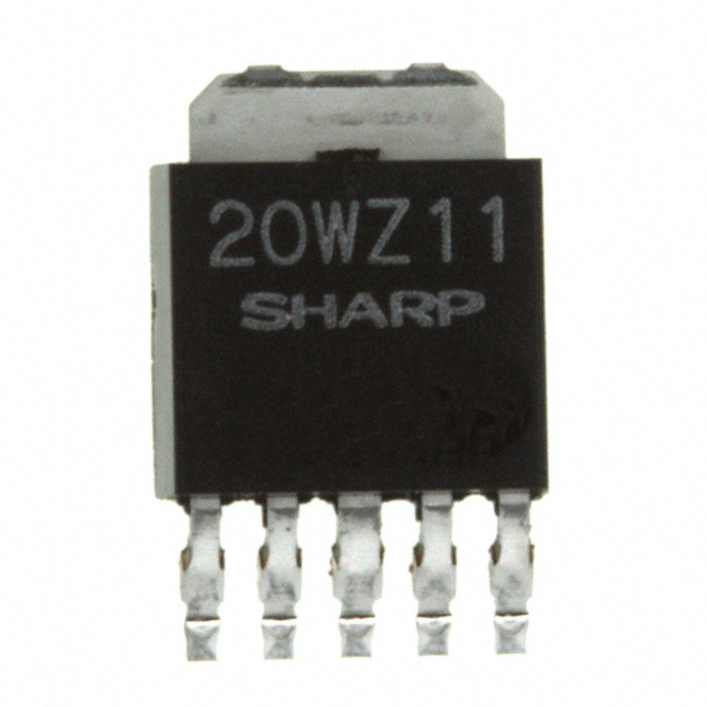
| 描述 | IC REG LDO ADJ 1A SC63 |
| 产品分类 | |
| 品牌 | Sharp Microelectronics |
| 数据手册 | http://www.sharpsma.com/webfm_send/1444 |
| 产品图片 |
|
| 产品型号 | PQ20WZ11J00H |
| rohs | 无铅 / 符合限制有害物质指令(RoHS)规范要求 |
| 产品系列 | - |
| 产品目录页面 | |
| 供应商器件封装 | SC-63 |
| 其它名称 | 425-2338-5 |
| 包装 | 管件 |
| 安装类型 | 表面贴装 |
| 封装/外壳 | TO-252-6,DPak(5 引线 + 接片) |
| 工作温度 | -20°C ~ 80°C |
| 标准包装 | 75 |
| 电压-跌落(典型值) | - |
| 电压-输入 | 3.5 V ~ 24 V |
| 电压-输出 | 3 V ~ 20 V |
| 电流-输出 | 1A |
| 电流-限制(最小值) | - |
| 稳压器拓扑 | 正,可调式 |
| 稳压器数 | 1 |


- 商务部:美国ITC正式对集成电路等产品启动337调查
- 曝三星4nm工艺存在良率问题 高通将骁龙8 Gen1或转产台积电
- 太阳诱电将投资9.5亿元在常州建新厂生产MLCC 预计2023年完工
- 英特尔发布欧洲新工厂建设计划 深化IDM 2.0 战略
- 台积电先进制程称霸业界 有大客户加持明年业绩稳了
- 达到5530亿美元!SIA预计今年全球半导体销售额将创下新高
- 英特尔拟将自动驾驶子公司Mobileye上市 估值或超500亿美元
- 三星加码芯片和SET,合并消费电子和移动部门,撤换高东真等 CEO
- 三星电子宣布重大人事变动 还合并消费电子和移动部门
- 海关总署:前11个月进口集成电路产品价值2.52万亿元 增长14.8%


PDF Datasheet 数据手册内容提取
PQ20WZ51J00H/PQ20WZ11J00H PQ20WZ51J00H PQ20WZ11J00H Variable Output,Surface Mount Type Low Power-Loss Voltage Regulators Features ■ Outline Dimensions (Unit : mm) 1.Low power-loss (Dropout voltage:MAX.0.5V) 2.Surface mount package 6.6MAX. 2.3±0.5 3.Output current (0.5A:PQ20WZ51J00H) 5.2±0.5 (0.5) 3 (1.0A:PQ20WZ11J00H) Epoxy resin 4.Reference voltage precision:±2.0% 20WZ51 Lead finish 56..VBaurilita-ibnl eO oNu/tOpFutF v cooltnatgroel( 3fu tnoc 2tio0nV) MAX. ±0.55.5 identification mark 7.Low dissipation current at OFF-state(Iqs:MAX.5μA) 9.7 H 1.7) ( 8.Built-in overcurrent and overheat protection functions N. (0~0.25) MI 9.RoHS directive compliant 2.5 0 . 5 +-00..12 (0.5) 9) 4–(1.27) 0. Applications ( ( ) : Typical dimensions 1.Personal computers Product mass:(0.3g) 2.CD-ROM drives 1 2 3 4 5 3.Power supplies for various OA equipment Internal connection diagram Model Line-up 1 3 ①②DOCN /iOnpFuFt c(oVnINtr)ol terminal (VC) Specific IC ③DC output (VO) Output Package 2 4 ④Output voltage adjustment Variable output 5 terminal (VADJ) current (IO) type ⑤GND Taping PQ20WZ5UJ00H Heat sink is common to terminal ③ (VO) 0.5A Sleeve PQ20WZ51J00H Taping PQ20WZ1UJ00H 1A Lead finish:Lead-free solder plating Sleeve PQ20WZ11J00H (Composition: Sn2Cu) Absolute Maximum Ratings (Ta=25°C) Parameter Symbol Rating Unit *1Input voltage VIN 24 V ON/OFF control terminal voltage VC 24 V *1Output adjustment terminal voltage VADJ 5 V Output PQ20WZ51J00H 0.5 current PQ20WZ11J00H IO 1 A *2Power dissipation PD 8 W *3Junction temperature Tj 150 ˚C Operating temperature Topr -20 to +80 ˚C Storage temperature Tstg -40 to +150 ˚C Soldering temperature Tsol 260(10s) ˚C *1 All are open except GND and applicable terminals. *2 PD: With infinite hea t sink *3 Overheat protection may operate at Tj:125°C to 150°C NoticeThe content of data sheet is subject to change without prior notice. In the absence of confirmation by device specification sheets, SHARP takes no responsibility for any defects that may occur in equipment using any SHARP devices shown in catalogs, data books, etc. Contact SHARP in order to obtain the latest device specification sheets before using any SHARP device. Sheet No.: OP06025 1
PQ20WZ51J00H/PQ20WZ11J00H Electrical Characteristics (Unless otherwise specified,condition shall be VIN=5V,VO=3.3, 4 ,R1=2kΩ,R2=500Ω,VC=2.7V,Ta=25°C) Parameter Symbol Conditions MIN. TYP. MAX. Unit Input voltage VIN - 3.5 - 24 V Output voltage VO - 3.0 - 20 V Load regulation RegL 5 - - 2.0 % Line regulation RegI VIN=4 to 10V , IO=5mA - - 2.5 % Ripple rejection RR Refer to Fig.2 45 60 - dB Reference voltage Vref 4 2.574 2.64 2.706 V Temperature coefficient of reference voltage TCVref Tj=0 to +125°C, IO=5mA - ±1.0 - % Dropout voltage VI-O 4, 6 - - 0.5 V - - Quiescent current Iq IO=0A 8 mA 7ON-state voltage for control VC(ON) - 2.0 - - V ON-state current for control IC(ON) - - - 200 μA OFF-state voltage for control VC(OFF) IO=0A - - 0.8 V OFF-state current for control IC(OFF) IO=0A,VC=0.4V - - 2.0 μA Output OFF-state consumption current Iqs IO=0A,VC=0.4V - - 5.0 μA 4 PQ20WZ51J00H:IO=0.3A,PQ20WZ11J00H:IO=0.5A 5 PQ20WZ51J00H:IO=5mA to 0.5A,PQ20WZ11J00H:IO=5mA to 1.0A 6 Input voltage shall be the value when output voltage is 95% in comparison with the initial value. 7In case of opening control terminal ② , output voltage turns off. Fig.1 Test Circuit VIN VO 1 3 R2 A IO VC Vref 2 + 4 5 V 0.33μF A 47μF IC A Iq R1 V RL 2kΩ VO=Vref×(1+R2/R1) [R1=2kΩ, VREF ≒ 2.64V] Fig.2 Test Circuit for Ripple Rejection + 1 3 ei ~ R2 IO VC 2 4 Vref + Veo ~ 0.33μF 5 47μF VIN R1 RL 2kΩ 2.7V f=120Hz (sine wave) ei(rms)=0.5V VIN=5V VO=3.3V(R1=2kΩ) IO=0.3A RR=20log(ei(rms)/eo(rms)) Sheet No.: OP06025 2
PQ20WZ51J00H/PQ20WZ11J00H Fig.3 Power Dissipation vs. Ambient Fig.4 Overcurrent Protection Characteristics Temperature (Typical Value)(PQ20WZ51J00H) 10 4 VO=3.3V W) PD:With infinite heat sink dissipation P (D 58 ut voltage V(V)O 32 VVVViiii––––OOOO====0123.VVV5V wer Outp o 1 P 0 0 -20 0 20 40 60 80 100 120 140150 0 0.5 1.0 1.5 2.0 Ambient temperature Ta (°C) Output current IO (A) Note) Oblique line portion:Overheat protection may operate in this area. Fig.5 Overcurrent Protection Characteristics Fig.6 Output Voltage Adjustment (Typical Value)(PQ20WZ11J00H) Characteristics 4 20 VO=3.3V Vi–O=0.5V R1=2kΩ V) 3 V)15 Output voltage V(O 21 VVViii–––OOO===123VVV Output voltage V(O 150 0 0 0 0.5 1.0 1.5 2.0 0.1 1 10 100 Output current IO (A) R2 (kΩ) Fig.7 Reference Voltage Deviation vs. Fig.8 Output Voltage vs. Input Voltage Junction Temperature (Typical Value) (PQ20WZ51J00H) 25 mV) 20 VVION==37.V3V(R1=2kΩ,R2=0.5kΩ) 8 RVC1==22k.7ΩV , R, C2=i=00.5.3k3ΩμF , C0=47μF (ef 15 IO=0.3A (PQ20WZ51J00H) 7 Tj=25°C oltage deviation ΔVr 1-5005 =0.5A (PQ20WZ11J00PHQ)20WZ11J00H ut Voltage V (V)O 5634 RL=∞Ω nce v--1150 PQ20WZ51J00H Outp 2 RL=11Ω e efer-20 1 RL=6.6Ω R -25 0 -25 0 25 50 75 100 125 0 1 2 3 4 5 6 7 8 Junction temperature Tj (˚C) Input Voltage VIN (V) Sheet No.: OP06025 3
PQ20WZ51J00H/PQ20WZ11J00H Fig.9 Output Voltage vs. Input Voltage Fig.10 Dropout Voltage vs. Junction (PQ20WZ11J00H) Temperature(PQ20WZ51J00H) 0.2 8 R1=2kΩ ,R2=0.5kΩ VIN=3.135V, Vc=2.7V, R1=2kΩ, R2=0.5kΩ, IO=0.3A VC=2.7V , Ci=0.33μF , C0=47μF 0.19 7 Tj=25°C V) 0.18 e V (V)O 56 age V(i-O 00..1167 utput Voltag 234 RL=∞Ω RL=6.6Ω Dropout volt 000...111543 O 0.12 1 RL=3.3Ω 0.11 0 0.1 0 1 2 3 4 5 6 7 8 -25 0 25 50 75 100 125 Input Voltage VIN (V) Junction temperature Tj (˚C) Fig.11 Dropout Voltage vs. Junction Fig.12 Quiescent Current vs. Junction Temperature(PQ20WZ11J00H) Temperature 0.18 5 VIN=5V 0.17 IO=0A ge V(V)i-O 00..1156 ent Iq(mA) 34 VRRC12===202k..57ΩkVΩ olta 0.14 curr out v 0.13 cent 2 p s o e Dr 0.12 ui Q 1 0.11 VIN=3.135V, Vc=2.7V, R1=2kΩ, R2=0.5kΩ, IO=0.5A 0.1 0 -25 0 25 50 75 100 125 -25 0 25 50 75 100 125 Junction temperature Tj (˚C) Junction temperature Tj (˚C) Fig.13 Ripple Rejection vs. Input Ripple Fig.14 Ripple Rejection vs. Output Frequency Current (PQ20WZ51J00H) 80 80 75 75 on RR (dB) 6750 PQ20WZ51J00H PQ20WZ11J00H n RR (dB) 6750 ecti 60 ctio 60 ej e ple r 55 e rej 55 Tj=25°C Rip 50 Tj=25°C IO=0.3A Rippl 50 VRI1N==25kVΩ 45 VRI1N==25kVΩ ,eRi(Rrm=s2)0= 0lo.g5(Vei((srmins)e/e wo(armvse))) 45 Rei2(r=m0s.)5=k0Ω.5V 40 R2=0.5kΩ 40 f=120Hz (sine wave) 0.1 1 10 100 0 0.1 0.2 0.3 0.4 0.5 0.6 0.70.8 0.9 1 Input ripple frequency f (kHz) Output current IO (A) Sheet No.: OP06025 4
PQ20WZ51J00H/PQ20WZ11J00H Fig.15 Ripple Rejection vs. Output Fig.16 Circuit Operating Current vs. Input Current (PQ20WZ11J00H) Voltage (PQ20WZ51J00H) 80 20 A) Vc=2.7V, 75 m R1=2kΩ, R2=0.5kΩ on RR (dB) 6750 urrent I (BIAS 15 (Vo=3.3V) Ripple rejecti 45565050 TVReRijI12(=Nr==m=22055sk.)V°5=ΩCk0Ω.5V Circuit operating c 105 RRRLLL ===61∞1.Ω6ΩΩ f=120Hz (sine wave) 40 0 0 0.1 0.2 0.3 0.4 0.5 0.6 0.70.8 0.9 1 0 1 2 3 4 5 6 Output current IO (A) Input voltage VIN (V) Fig.17 Circuit Operating Current vs. Input Voltage (PQ20WZ11J00H) 30 Vc=2.7V, mA) R1=2kΩ, R2=0.5kΩ (S 25 (Vo=3.3V) A BI ent I 20 RL=3.3Ω urr c 15 g n erati 10 RL=6.6Ω p o uit 5 RL= ∞Ω c Cir 0 0 1 2 3 4 5 6 7 8 Input voltage VIN (V) Fig.18 Power Dissipation vs. Ambient Temperature 3 W) Cu area 740mm2 (D P 2 n Mounting PCB o ati Cu area 180mm2 PCB p si Cu area 100mm2 Cu s di Cu area 70mm2 er 1 w Cu area 36mm2 Po Material : Glass-cloth epoxy resin Size : 50×50×1.6mm Cu thickness : 35μm 0 -20 0 20 40 60 80 100 Ambient temperature Ta (°C) Sheet No.: OP06025 5
PQ20WZ51J00H/PQ20WZ11J00H ■ Setting of Output Voltage Output voltage is able to set from 3V to 20V when resistors R1 and R2 are attached to ,③、④、⑤ terminals. As for the external resistors to set output voltage, refer to the figure below and Fig.6. VO 3 R2 VO=Vref×1+R2/R1 4 (R1=2kΩ,Vref≒2.64V) + R1 5 Vref ■ Typical Application DC Input 1 3 VO R2 CO + VIN CIN 2 4 5 47μF Load R1 2kΩ ON/OFF signal ⎞⎟ High:Output ON ⎞⎟ ⎠ Low or Open:Output OFF ⎠ Sheet No.: OP06025 6