ICGOO在线商城 > 分立半导体产品 > 二极管 - 整流器 - 单 > PMEG4010BEA,135
 Datasheet下载
- 型号: PMEG4010BEA,135
- 制造商: NXP Semiconductors
- 库位|库存: xxxx|xxxx
- 要求:
| 数量阶梯 | 香港交货 | 国内含税 |
| +xxxx | $xxxx | ¥xxxx |
查看当月历史价格
查看今年历史价格
PMEG4010BEA,135产品简介:
ICGOO电子元器件商城为您提供PMEG4010BEA,135由NXP Semiconductors设计生产,在icgoo商城现货销售,并且可以通过原厂、代理商等渠道进行代购。 PMEG4010BEA,135价格参考。NXP SemiconductorsPMEG4010BEA,135封装/规格:二极管 - 整流器 - 单, 肖特基 表面贴装 二极管 40V 1A(DC) SOD-323。您可以下载PMEG4010BEA,135参考资料、Datasheet数据手册功能说明书,资料中有PMEG4010BEA,135 详细功能的应用电路图电压和使用方法及教程。
PMEG4010BEA,135 是 Nexperia USA Inc. 生产的一款单个整流二极管,广泛应用于各种电力转换和保护电路中。其主要应用场景包括:

1. 电源适配器和充电器:在电源适配器和充电器中,该二极管用于将交流电(AC)转换为直流电(DC),以确保输出稳定的电压和电流。它能够承受较高的反向电压和较大的正向电流,适用于笔记本电脑、手机等设备的充电电路。

2. 开关电源(SMPS):在开关电源中,PMEG4010BEA,135 用于整流部分,将高频交流信号转换为直流信号。它具有低正向压降和快速恢复特性,能够提高电源效率并减少能量损耗。

3. 电机驱动电路:在电机驱动电路中,该二极管可以作为续流二极管,用于吸收电机绕组中的感应电流,防止电流突变对电路造成损坏。它能够有效保护晶体管和其他敏感元件,延长系统的使用寿命。

4. 太阳能逆变器:在太阳能发电系统中,该二极管用于将太阳能电池板产生的直流电转换为交流电,并将其馈入电网或负载。它能够在高电压和大电流条件下稳定工作,确保系统的高效运行。

5. 汽车电子系统:在汽车电子系统中,PMEG4010BEA,135 可用于车载充电器、发电机整流桥等应用,确保车辆电气系统的稳定性和可靠性。它具有良好的耐高温性能和抗干扰能力,适合复杂的汽车环境。

6. 工业控制和自动化设备:在工业控制系统中,该二极管用于电源模块和信号处理电路中,提供稳定的直流电源和保护功能。它能够承受恶劣的工作环境,确保设备的长期稳定运行。

总之,PMEG4010BEA,135 凭借其优异的电气性能和可靠性,广泛应用于各类电力转换和保护电路中,特别是在需要高效整流和大电流承载能力的场合。
| 参数 | 数值 |
| 产品目录 | |
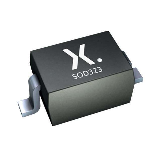
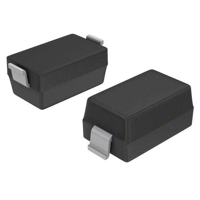
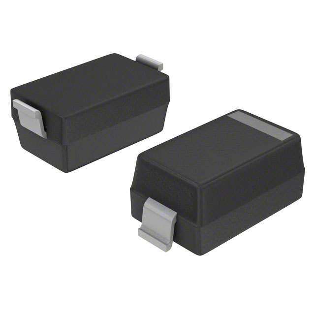
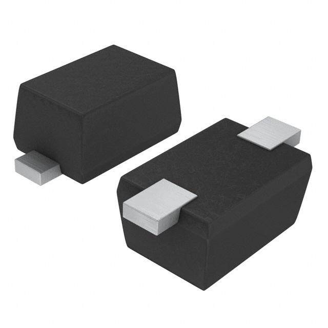
| 描述 | DIODE SCHOTTKY 40V 1A SOD323 |
| 产品分类 | 单二极管/整流器 |
| 品牌 | NXP Semiconductors |
| 数据手册 | |
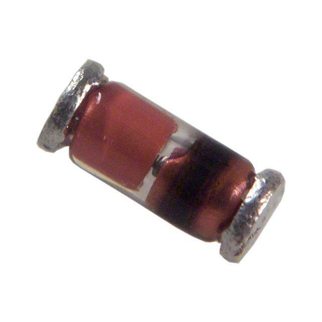
| 产品图片 |
|
| 产品型号 | PMEG4010BEA,135 |
| PCN封装 | |
| PCN设计/规格 | |
| rohs | 无铅 / 符合限制有害物质指令(RoHS)规范要求 |
| 产品系列 | - |
| 不同If时的电压-正向(Vf) | 640mV @ 1A |
| 不同 Vr、F时的电容 | 50pF @ 1V,1MHz |
| 不同 Vr时的电流-反向漏电流 | 100µA @ 40V |
| 二极管类型 | |
| 供应商器件封装 | SOD-323 |
| 其它名称 | 568-10388-2 |
| 包装 | 带卷 (TR) |
| 反向恢复时间(trr) | - |
| 安装类型 | 表面贴装 |
| 封装/外壳 | SC-76,SOD-323 |
| 工作温度-结 | 150°C (最大) |
| 标准包装 | 10,000 |
| 热阻 | 90°C/W Jl |
| 电压-DC反向(Vr)(最大值) | 40V |
| 电流-平均整流(Io) | 1A(DC) |
| 速度 | 快速恢复 =< 500 ns,> 200mA(Io) |


- 商务部:美国ITC正式对集成电路等产品启动337调查
- 曝三星4nm工艺存在良率问题 高通将骁龙8 Gen1或转产台积电
- 太阳诱电将投资9.5亿元在常州建新厂生产MLCC 预计2023年完工
- 英特尔发布欧洲新工厂建设计划 深化IDM 2.0 战略
- 台积电先进制程称霸业界 有大客户加持明年业绩稳了
- 达到5530亿美元!SIA预计今年全球半导体销售额将创下新高
- 英特尔拟将自动驾驶子公司Mobileye上市 估值或超500亿美元
- 三星加码芯片和SET,合并消费电子和移动部门,撤换高东真等 CEO
- 三星电子宣布重大人事变动 还合并消费电子和移动部门
- 海关总署:前11个月进口集成电路产品价值2.52万亿元 增长14.8%


PDF Datasheet 数据手册内容提取
Important notice Dear Customer, On 7 February 2017 the former NXP Standard Product business became a new company with the tradename Nexperia. Nexperia is an industry leading supplier of Discrete, Logic and PowerMOS semiconductors with its focus on the automotive, industrial, computing, consumer and wearable application markets In data sheets and application notes which still contain NXP or Philips Semiconductors references, use the references to Nexperia, as shown below. Instead of http://www.nxp.com, http://www.philips.com/ or http://www.semiconductors.philips.com/, use http://www.nexperia.com Instead of sales.addresses@www.nxp.com or sales.addresses@www.semiconductors.philips.com, use salesaddresses@nexperia.com (email) Replace the copyright notice at the bottom of each page or elsewhere in the document, depending on the version, as shown below: - © NXP N.V. (year). All rights reserved or © Koninklijke Philips Electronics N.V. (year). All rights reserved Should be replaced with: - © Nexperia B.V. (year). All rights reserved. If you have any questions related to the data sheet, please contact our nearest sales office via e-mail or telephone (details via salesaddresses@nexperia.com). Thank you for your cooperation and understanding, Kind regards, Team Nexperia
DISCRETE SEMICONDUCTORS DATA SHEET PMEGXX10BEA; PMEGXX10BEV 1 A very low V MEGA Schottky F barrier rectifier Product data sheet 2004 Jun 14 Supersedes data of 2004 Apr 02
NXP Semiconductors Product data sheet 1 A very low V MEGA Schottky PMEGXX10BEA; F barrier rectifier PMEGXX10BEV FEATURES QUICK REFERENCE DATA • Forward current: 1 A SYMBOL PARAMETER MAX. UNIT • Reverse voltages: 20 V, 30 V, 40 V I forward current 1 A F • Very low forward voltage V reverse voltage 20; 30; 40 V R • Ultra small and very small plastic SMD package • Power dissipation comparable to SOT23. PINNING PIN DESCRIPTION APPLICATIONS PMEGXX10BEA (see Fig.1) • High efficiency DC-to-DC conversion 1 cathode • Voltage clamping 2 anode • Protection circuits PMEGXX10BEV (see Fig.2) • Low voltage rectification 1, 2, 5, 6 cathode • Blocking diodes 3, 4 anode • Low power consumption applications. DESCRIPTION Planar Maximum Efficiency General Application (MEGA) 1 2 Schottky barrier rectifier with an integrated guard ring for 1 2 stress protection, encapsulated in a very small SOD323 (SC-76) and ultra small SOT666 SMD plastic package. sym001 MARKING TYPE NUMBER MARKING CODE The marking bar indicates the cathode. PMEG2010BEA V1 Fig.1 Simplified outline (SOD323; SC-76) and PMEG3010BEA V2 symbol. PMEG4010BEA V3 PMEG2010BEV G6 PMEG3010BEV G5 PMEG4010BEV G4 6 5 4 1,2 3, 4 5,6 sym038 1 2 3 Fig.2 Simplified outline (SOT666) and symbol. 2004 Jun 14 2
NXP Semiconductors Product data sheet 1 A very low V MEGA Schottky PMEGXX10BEA; F barrier rectifier PMEGXX10BEV ORDERING INFORMATION PACKAGE TYPE NUMBER NAME DESCRIPTION VERSION PMEGXX10BEA − plastic surface mounted package; 2 leads SOD323 PMEGXX10BEV plastic surface mounted package; 6 leads SOT666 LIMITING VALUES In accordance with the Absolute Maximum Rating System (IEC 60134). SYMBOL PARAMETER CONDITIONS MIN. MAX. UNIT V continuous reverse voltage R PMEG2010BEA/PMEG2010BEV − 20 V PMEG3010BEA/PMEG3010BEV − 30 V PMEG4010BEA/PMEG4010BEV − 40 V I continuous forward current T ≤ 55 °C; note 1 − 1 A F s I repetitive peak forward current t ≤ 1 ms; δ ≤ 0.5; note 2 − 3.5 A FRM p I non-repetitive peak forward current t = 8 ms; square wave; − 10 A FSM p note 2 T junction temperature note 3 − 150 °C j T operating ambient temperature note 3 −65 +150 °C amb T storage temperature −65 +150 °C stg Notes 1. Refer to SOD323 (SC-76) and SOT666 standard mounting conditions. 2. Only valid if pins 3 and 4 are connected in parallel (SOT666 package). 3. For Schottky barrier diodes thermal runaway has to be considered, as in some applications the reverse power losses P are a significant part of the total power losses. Nomograms for determining the reverse power losses P and I R R F(AV) rating will be available on request. 2004 Jun 14 3
NXP Semiconductors Product data sheet 1 A very low V MEGA Schottky PMEGXX10BEA; F barrier rectifier PMEGXX10BEV THERMAL CHARACTERISTICS SYMBOL PARAMETER CONDITIONS VALUE UNIT PMEGXX10BEA (SOD323) R thermal resistance from junction to in free air; notes 1 and 2 450 K/W th(j-a) ambient in free air; notes 2 and 3 210 K/W R thermal resistance from junction to note 4 90 K/W th(j-s) soldering point PMEGXX10BEV (SOT666) R thermal resistance from junction to in free air; notes 2 and 5 405 K/W th(j-a) ambient in free air; notes 2 and 6 215 K/W R thermal resistance from junction to note 4 80 K/W th(j-s) soldering point Notes 1. Refer to SOD323 (SC-76) standard mounting conditions. 2. For Schottky barrier diodes thermal runaway has to be considered, as in some applications the reverse power losses P are a significant part of the total power losses. Nomograms for determining the reverse power losses P and I R R F(AV) rating will be available on request. 3. Device mounted on an FR4 printed-circuit board with copper clad 10 × 10 mm. 4. Solder point of cathode tab. 5. Refer to SOT666 standard mounting conditions. 6. Only valid if pins 3 and 4 are connected in parallel (SOT666 package). CHARACTERISTICS T = 25 °C unless otherwise specified. amb PMEG2010BEA/ PMEG3010BEA/ PMEG4010BEA/ PMEG2010BEV PMEG3010BEV PMEG4010BEV SYMBOL PARAMETER CONDITIONS UNIT TYP. MAX. TYP. MAX. TYP. MAX. V forward voltage I = 0.1 mA 90 130 90 130 95 130 mV F F I = 1 mA 150 190 150 200 155 210 mV F I = 10 mA 210 240 215 250 220 270 mV F I = 100 mA 280 330 285 340 295 350 mV F I = 500 mA 355 390 380 430 420 470 mV F I = 1 000 mA 420 500 450 560 540 640 mV F I continuous V = 10 V; note 1 15 40 12 30 7 20 μA R R reverse current V = 20 V; note 1 40 200 − − − − μA R V = 30 V; note 1 − − 40 150 − − μA R V = 40 V; note 1 − − − − 30 100 μA R C diode capacitance V = 1 V; f = 1 MHz 66 80 55 70 43 50 pF d R Note 1. Pulse test: t ≤ 300 μs; δ ≤ 0.02. p 2004 Jun 14 4
NXP Semiconductors Product data sheet 1 A very low V MEGA Schottky PMEGXX10BEA; F barrier rectifier PMEGXX10BEV GRAPHICAL DATA 104 MHC673 105 MHC674 handbook, halfpage handbook, halfpage IF IR (mA) (μA) (1) 103 104 102 (1) (2) (3) 103 (2) 10 102 (3) 1 10 10−1 1 0 0.2 0.4 0.6 0 5 10 15 20 VF (V) VR (V) PMEG2010BEA/PMEG2010BEV PMEG2010BEA/PMEG2010BEV (1) Tamb = 150 °C. (1) Tamb = 150 °C. (2) Tamb = 85 °C. (2) Tamb = 85 °C. (3) Tamb = 25 °C. (3) Tamb = 25 °C. Fig.3 Forward current as a function of forward Fig.4 Reverse current as a function of reverse voltage; typical values. voltage; typical values. 140 MHC675 104 MHC676 handbCoodk, halfpage handbooIkF, halfpage (pF) (mA) 120 103 100 102 (1) (2) (3) 80 60 10 40 1 20 0 10−1 0 5 10 15 20 0 0.2 0.4 0.6 VR (V) VF (V) PMEG3010BEA/PMEG3010BEV (1) Tamb = 150 °C. PMEG2010BEA/PMEG2010BEV (2) Tamb = 85 °C. Tamb = 25 °C; f = 1 MHz. (3) Tamb = 25 °C. Fig.5 Diode capacitance as a function of reverse Fig.6 Forward current as a function of forward voltage; typical values. voltage; typical values. 2004 Jun 14 5
NXP Semiconductors Product data sheet 1 A very low V MEGA Schottky PMEGXX10BEA; F barrier rectifier PMEGXX10BEV 105 MHC677 120 MHC678 IR handbCoodk, halfpage (μA) (1) (pF) 100 104 80 103 (2) 60 102 40 (3) 10 20 1 0 0 5 10 15 20 25 30 0 5 10 15 20 VR (V) VR (V) PMEG3010BEA/PMEG3010BEV (1) Tamb = 150 °C. (2) Tamb = 85 °C. PMEG3010BEA/PMEG3010BEV (3) Tamb = 25 °C. Tamb = 25 °C; f = 1 MHz. Fig.7 Reverse current as a function of reverse Fig.8 Diode capacitance as a function of reverse voltage; typical values. voltage; typical values. 104 MHC679 105 MHC680 handbooIkF, halfpage handboIoRk, halfpage (mA) (μA) (1) 103 104 102 (1) (2) (3) 103 (2) 10 102 1 10 (3) 10−1 1 0 0.2 0.4 0.6 0 10 20 30 40 VF (V) VR (V) PMEG4010BEA/PMEG4010BEV PMEG4010BEA/PMEG4010BEV (1) Tamb = 150 °C. (1) Tamb = 150 °C. (2) Tamb = 85 °C. (2) Tamb = 85 °C. (3) Tamb = 25 °C. (3) Tamb = 25 °C. Fig.9 Forward current as a function of forward Fig.10 Reverse current as a function of reverse voltage; typical values. voltage; typical values. 2004 Jun 14 6
NXP Semiconductors Product data sheet 1 A very low V MEGA Schottky PMEGXX10BEA; F barrier rectifier PMEGXX10BEV MHC681 100 handbook, halfpage Cd (pF) 80 60 40 20 0 0 5 10 15 20 VR (V) PMEG4010BEA/PMEG4010BEV Tamb = 25 °C; f = 1 MHz. Fig.11 Diode capacitance as a function of reverse voltage; typical values. 2004 Jun 14 7
NXP Semiconductors Product data sheet 1 A very low V MEGA Schottky PMEGXX10BEA; F barrier rectifier PMEGXX10BEV PACKAGE OUTLINES Plastic surface-mounted package; 2 leads SOD323 D A E X HD v M A Q 1 2 bp A A1 (1) c Lp detail X 0 1 2 mm scale DIMENSIONS (mm are the original dimensions) UNIT A mAa1x bp c D E HD Lp Q v 1.1 0.40 0.25 1.8 1.35 2.7 0.45 0.25 mm 0.05 0.2 0.8 0.25 0.10 1.6 1.15 2.3 0.15 0.15 Note 1. The marking bar indicates the cathode OUTLINE REFERENCES EUROPEAN ISSUE DATE VERSION IEC JEDEC JEITA PROJECTION 03-12-17 SOD323 SC-76 06-03-16 2004 Jun 14 8
NXP Semiconductors Product data sheet 1 A very low V MEGA Schottky PMEGXX10BEA; F barrier rectifier PMEGXX10BEV Plastic surface-mounted package; 6 leads SOT666 D A E X S Y S HE 6 5 4 pin 1 index A 1 2 3 c e1 bp w M A Lp e detail X 0 1 2 mm scale DIMENSIONS (mm are the original dimensions) UNIT A bp c D E e e1 HE Lp w y 0.6 0.27 0.18 1.7 1.3 1.7 0.3 mm 1.0 0.5 0.1 0.1 0.5 0.17 0.08 1.5 1.1 1.5 0.1 OUTLINE REFERENCES EUROPEAN ISSUE DATE VERSION IEC JEDEC JEITA PROJECTION 04-11-08 SOT666 06-03-16 2004 Jun 14 9
NXP Semiconductors Product data sheet 1 A very low V MEGA Schottky PMEGXX10BEA; F barrier rectifier PMEGXX10BEV DATA SHEET STATUS DOCUMENT PRODUCT DEFINITION STATUS(1) STATUS(2) Objective data sheet Development This document contains data from the objective specification for product development. Preliminary data sheet Qualification This document contains data from the preliminary specification. Product data sheet Production This document contains the product specification. Notes 1. Please consult the most recently issued document before initiating or completing a design. 2. The product status of device(s) described in this document may have changed since this document was published and may differ in case of multiple devices. The latest product status information is available on the Internet at URL http://www.nxp.com. DISCLAIMERS above those given in the Characteristics sections of this document is not implied. Exposure to limiting values for General ⎯ Information in this document is believed to be extended periods may affect device reliability. accurate and reliable. However, NXP Semiconductors does not give any representations or warranties, Terms and conditions of sale ⎯ NXP Semiconductors expressed or implied, as to the accuracy or completeness products are sold subject to the general terms and of such information and shall have no liability for the conditions of commercial sale, as published at consequences of use of such information. http://www.nxp.com/profile/terms, including those pertaining to warranty, intellectual property rights Right to make changes ⎯ NXP Semiconductors infringement and limitation of liability, unless explicitly reserves the right to make changes to information otherwise agreed to in writing by NXP Semiconductors. In published in this document, including without limitation case of any inconsistency or conflict between information specifications and product descriptions, at any time and in this document and such terms and conditions, the latter without notice. This document supersedes and replaces all will prevail. information supplied prior to the publication hereof. No offer to sell or license ⎯ Nothing in this document Suitability for use ⎯ NXP Semiconductors products are may be interpreted or construed as an offer to sell products not designed, authorized or warranted to be suitable for that is open for acceptance or the grant, conveyance or use in medical, military, aircraft, space or life support implication of any license under any copyrights, patents or equipment, nor in applications where failure or malfunction other industrial or intellectual property rights. of an NXP Semiconductors product can reasonably be expected to result in personal injury, death or severe Export control ⎯ This document as well as the item(s) property or environmental damage. NXP Semiconductors described herein may be subject to export control accepts no liability for inclusion and/or use of NXP regulations. Export might require a prior authorization from Semiconductors products in such equipment or national authorities. applications and therefore such inclusion and/or use is at Quick reference data ⎯ The Quick reference data is an the customer’s own risk. extract of the product data given in the Limiting values and Applications ⎯ Applications that are described herein for Characteristics sections of this document, and as such is any of these products are for illustrative purposes only. not complete, exhaustive or legally binding. NXP Semiconductors makes no representation or warranty that such applications will be suitable for the specified use without further testing or modification. Limiting values ⎯ Stress above one or more limiting values (as defined in the Absolute Maximum Ratings System of IEC 60134) may cause permanent damage to the device. Limiting values are stress ratings only and operation of the device at these or any other conditions 2004 Jun 14 10
NXP Semiconductors Customer notification This data sheet was changed to reflect the new company name NXP Semiconductors, including new legal definitions and disclaimers. No changes were made to the technical content, except for package outline drawings which were updated to the latest version. Contact information For additional information please visit: http://www.nxp.com For sales offices addresses send e-mail to: salesaddresses@nxp.com © NXP B.V. 2009 All rights are reserved. Reproduction in whole or in part is prohibited without the prior written consent of the copyright owner. The information presented in this document does not form part of any quotation or contract, is believed to be accurate and reliable and may be changed without notice. No liability will be accepted by the publisher for any consequence of its use. Publication thereof does not convey nor imply any license under patent- or other industrial or intellectual property rights. Printed in The Netherlands R76/04/pp11 Date of release: 2004 Jun 14 Document order number: 9397 750 13234