ICGOO在线商城 > PMDPB80XP,115

 Datasheet下载
- 型号: PMDPB80XP,115
- 制造商: NXP Semiconductors
- 库位|库存: xxxx|xxxx
- 要求:
| 数量阶梯 | 香港交货 | 国内含税 |
| +xxxx | $xxxx | ¥xxxx |
查看当月历史价格
查看今年历史价格
PMDPB80XP,115产品简介:
ICGOO电子元器件商城为您提供PMDPB80XP,115由NXP Semiconductors设计生产,在icgoo商城现货销售,并且可以通过原厂、代理商等渠道进行代购。 提供PMDPB80XP,115价格参考以及NXP SemiconductorsPMDPB80XP,115封装/规格参数等产品信息。 你可以下载PMDPB80XP,115参考资料、Datasheet数据手册功能说明书, 资料中有PMDPB80XP,115详细功能的应用电路图电压和使用方法及教程。
| 参数 | 数值 |
| 产品目录 | |
| ChannelMode | Enhancement |
| 描述 | MOSFET 2P-CH 20V 2.7A HUSON6MOSFET 20V, Dual P-Channel Trench MOSFET |
| 产品分类 | FET - 阵列分离式半导体 |
| FET功能 | 逻辑电平栅极,1.8V 驱动 |
| FET类型 | 2 个 P 沟道(双) |
| Id-ContinuousDrainCurrent | - 3.7 A |
| Id-连续漏极电流 | - 3.7 A |
| 品牌 | NXP Semiconductors |
| 产品手册 | |
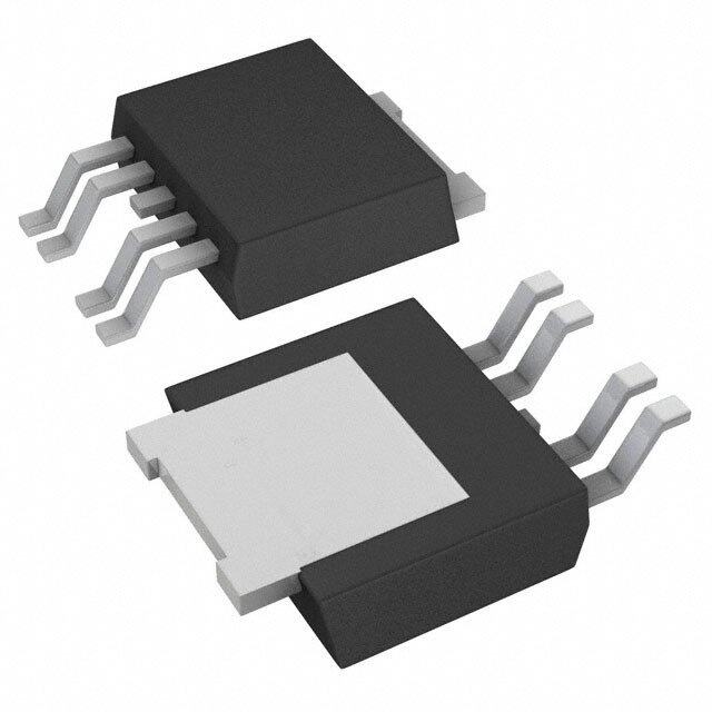
| 产品图片 |
|
| 产品系列 | 晶体管,MOSFET,NXP Semiconductors PMDPB80XP,115- |
| 数据手册 | |
| 产品型号 | PMDPB80XP,115 |
| Pd-PowerDissipation | 6250 mW |
| Pd-功率耗散 | 6.25 W |
| Qg-GateCharge | 5.7 nC |
| Qg-栅极电荷 | 5.7 nC |
| RdsOn-Drain-SourceResistance | 80 mOhms |
| RdsOn-漏源导通电阻 | 80 mOhms |
| rohs | 无铅 / 符合限制有害物质指令(RoHS)规范要求 |
| Vds-Drain-SourceBreakdownVoltage | - 20 V |
| Vds-漏源极击穿电压 | - 20 V |
| Vgsth-Gate-SourceThresholdVoltage | - 0.6 V |
| Vgsth-栅源极阈值电压 | - 0.6 V |
| 上升时间 | 14 ns |
| 下降时间 | 50 ns |
| 不同Id时的Vgs(th)(最大值) | 1V @ 250µA |
| 不同Vds时的输入电容(Ciss) | 550pF @ 10V |
| 不同Vgs时的栅极电荷(Qg) | 8.6nC @ 4.5V |
| 不同 Id、Vgs时的 RdsOn(最大值) | 102 毫欧 @ 2.7A, 4.5V |
| 产品种类 | MOSFET |
| 供应商器件封装 | 6-HUSON(2X2) |
| 其它名称 | 568-10763-6 |
| 典型关闭延迟时间 | 120 ns |
| 功率-最大值 | 485mW |
| 包装 | Digi-Reel® |
| 商标 | NXP Semiconductors |
| 安装类型 | 表面贴装 |
| 安装风格 | SMD/SMT |
| 封装 | Reel |
| 封装/外壳 | 6-UDFN 裸露焊盘 |
| 封装/箱体 | DFN2020-6 |
| 工厂包装数量 | 3000 |
| 晶体管极性 | P-Channel |
| 最大工作温度 | + 150 C |
| 最小工作温度 | - 55 C |
| 标准包装 | 1 |
| 漏源极电压(Vdss) | 20V |
| 电流-连续漏极(Id)(25°C时) | 2.7A |
| 通道模式 | Enhancement |
| 配置 | Dual |


.GN.jpg)


PDF Datasheet 数据手册内容提取
PMDPB80XP 20 V, dual P-channel Trench MOSFET Rev. 1 — 30 May 2012 Product data sheet 1. Product profile 1.1 General description Dual P-channel enhancement mode Field-Effect Transistor (FET) in a small and leadless ultra thin DFN2020-6 (SOT1118) Surface-Mounted Device (SMD) plastic package using Trench MOSFET technology. 1.2 Features and benefits 1.8 V R rated for low voltage Small and leadless ultra thin SMD DSon gate drive plastic package: 2 x 2 x 0.65 mm Trench MOSFET technology Exposed drain pad for excellent thermal conduction 1.3 Applications Charging switch for portable devices Power management in battery-driven portables DC/DC converters Hard disc and computing power Small brushless DC motor drive management 1.4 Quick reference data Table 1. Quick refere nce data Symbol Parameter Conditions Min Typ Max Unit Per transistor V drain-source voltage T =25°C - - -20 V DS j V gate-source voltage -12 - 12 V GS I drain current V =-4.5V; T =25°C; t ≤ 5 s [1] - - -3.7 A D GS amb Static characteristics (per transistor) R drain-source on-state V =-4.5V; I =-2.7A; T =25°C - 80 102 mΩ DSon GS D j resistance [1] Device mounted on an FR4 Printed-Circuit Board (PCB), single-sided copper, tin-plated, mounting pad for drain 6 cm2.
PMDPB80XP Nexperia 20 V, dual P-channel Trench MOSFET 2. Pinning information Table 2. Pinning infor mation Pin Symbol Description Simplified outline Graphic symbol 1 S1 source TR1 6 5 4 D1 D2 2 G1 gate TR1 3 D2 drain TR2 4 S2 source TR2 7 8 5 G2 gate TR2 6 D1 drain TR1 1 2 3 G1 S1 S2 G2 7 D1 drain TR1 Transparent top view 017aaa258 SOT1118 (DFN2020-6) 8 D2 drain TR2 3. Ordering information Table 3. Ordering info rmation Type number Package Name Description Version PMDPB80XP DFN2020-6 plastic thermal enhanced ultra thin small outline package; SOT1118 no leads; 6 terminals 4. Marking Table 4. Marking cod es Type number Marking code PMDPB80XP 1U PMDPB80XP All information provided in this document is subject to legal disclaimers. © Nexperia B.V. 2017. All rights reserved Product data sheet Rev. 1 — 30 May 2012 2 of 15
PMDPB80XP Nexperia 20 V, dual P-channel Trench MOSFET 5. Limiting values Table 5. Limiting valu es In accordance with the Absolute Maximum Rating System (IEC 60134). Symbol Parameter Conditions Min Max Unit Per transistor V drain-source voltage T =25°C - -20 V DS j V gate-source voltage -12 12 V GS I drain current V =-4.5V; T =25°C; t ≤ 5 s [1] - -3.7 A D GS amb V =-4.5V; T =25°C [1] - -2.7 A GS amb V =-4.5V; T =100°C [1] - -1.7 A GS amb I peak drain current T =25°C; single pulse; t ≤10µs - -11 A DM amb p P total power dissipation T =25°C [2] - 485 mW tot amb [1] - 1100 mW T =25°C - 6250 mW sp Source-drain diode I source current T =25°C [1] - -1.1 A S amb Per device T junction temperature -55 150 °C j T ambient temperature -55 150 °C amb T storage temperature -65 150 °C stg [1] Device mounted on an FR4 Printed-Circuit Board (PCB), single-sided copper, tin-plated, mounting pad for drain 6 cm2. [2] Device mounted on an FR4 Printed-Circuit Board (PCB), single-sided copper, tin-plated and standard footprint. 017aaa123 017aaa124 120 120 Pder Ider (%) (%) 80 80 40 40 0 0 −75 −25 25 75 125 175 −75 −25 25 75 125 175 Tj (°C) Tj (°C) Fig 1. Normalized total power dissipation as a Fig 2. Normalized continuous drain current as a function of junction temperature function of junction temperature PMDPB80XP All information provided in this document is subject to legal disclaimers. © Nexperia B.V. 2017. All rights reserved Product data sheet Rev. 1 — 30 May 2012 3 of 15
PMDPB80XP Nexperia 20 V, dual P-channel Trench MOSFET 017aaa563 -102 ID (A) Limit RDSon = VDS/ID -10 tp = 10 μs tp = 100 μs -1 tp = 10 ms DC; Tsp = 25 °C tp = 100 ms -10-1 DC; Tamb = 25 °C; drain mounting pad 6 cm2 -10-2 -10-1 -1 -10 -102 VDS (V) I = single pulse DM Fig 3. Safe operating area; junction to ambient; continuous and peak drain currents as a function of drain-source voltage 6. Thermal characteristics Table 6. Thermal cha racteristics Symbol Parameter Conditions Min Typ Max Unit Per transistor R thermal resistance in free air [1] - 225 260 K/W th(j-a) from junction to [2] - 99 115 K/W ambient in free air; t ≤ 5 s [2] - 54 62 K/W R thermal resistance in free air - 16 20 K/W th(j-sp) from junction to solder point [1] Device mounted on an FR4 PCB, single-sided copper, tin-plated and standard footprint. [2] Device mounted on an FR4 PCB, single-sided copper, tin-plated, mounting pad for drain 6 cm2. PMDPB80XP All information provided in this document is subject to legal disclaimers. © Nexperia B.V. 2017. All rights reserved Product data sheet Rev. 1 — 30 May 2012 4 of 15
PMDPB80XP Nexperia 20 V, dual P-channel Trench MOSFET 017aaa564 103 Zth(j-a) duty cycle = 1 (K/W) 0.75 102 0.5 0.33 0.25 0.2 0.1 10 0.05 0.02 0.01 1 0 10-1 10-5 10-4 10-3 10-2 10-1 1 10 102 103 tp (s) FR4 PCB, standard footprint Fig 4. Transient thermal impedance from junction to ambient as a function of pulse duration; typical values 017aaa565 103 Zth(j-a) (K/W) duty cycle = 1 102 0.75 0.5 0.33 0.25 0.2 10 0.1 0.05 0.02 1 0.01 0 10-1 10-5 10-4 10-3 10-2 10-1 1 10 102 103 tp (s) FR4 PCB, mounting pad for drain 6 cm2 Fig 5. Transient thermal impedance from junction to ambient as a function of pulse duration; typical values PMDPB80XP All information provided in this document is subject to legal disclaimers. © Nexperia B.V. 2017. All rights reserved Product data sheet Rev. 1 — 30 May 2012 5 of 15
PMDPB80XP Nexperia 20 V, dual P-channel Trench MOSFET 7. Characteristics Table 7. Characterist ics Symbol Parameter Conditions Min Typ Max Unit Static characteristics (per transistor) V drain-source I =-250µA; V =0V; T =25°C -20 - - V (BR)DSS D GS j breakdown voltage V gate-source threshold I =-250µA; V =V ; T =25°C -0.4 -0.6 -1 V GSth D DS GS j voltage I drain leakage current V =-20V; V =0V; T =25°C - - -1 µA DSS DS GS j V =-20V; V =0V; T =150°C - - -10 µA DS GS j I gate leakage current V =12V; V =0V; T =25°C - - 100 nA GSS GS DS j V =-12V; V =0V; T =25°C - - 100 nA GS DS j R drain-source on-state V =-4.5V; I =-2.7A; T =25°C - 80 102 mΩ DSon GS D j resistance V =-4.5V; I =-2.7A; T =150°C - 116 148 mΩ GS D j V =-2.5V; I =-2.5A; T =25°C - 95 125 mΩ GS D j V =-1.8V; I =-1.1A; T =25°C - 120 156 mΩ GS D j g forward V =-10V; I =-2.7A; T =25°C - 15 - S fs DS D j transconductance Dynamic characteristics (per transistor) Q total gate charge V =-10V; I =-2.7A; V =-4.5V; - 5.7 8.6 nC G(tot) DS D GS T =25°C Q gate-source charge j - 0.7 - nC GS Q gate-drain charge - 0.96 - nC GD C input capacitance V =-10V; f=1MHz; V =0V; - 550 - pF iss DS GS T =25°C C output capacitance j - 63 - pF oss C reverse transfer - 53 - pF rss capacitance t turn-on delay time V =-10V; I =-2.7A; V =-4.5V; - 6 - ns d(on) DS D GS R =6Ω; T =25°C t rise time G(ext) j - 14 - ns r t turn-off delay time - 120 - ns d(off) t fall time - 50 - ns f Source-drain diode (per transistor) V source-drain voltage I =-1.1A; V =0V; T =25°C - -0.8 -1.2 V SD S GS j PMDPB80XP All information provided in this document is subject to legal disclaimers. © Nexperia B.V. 2017. All rights reserved Product data sheet Rev. 1 — 30 May 2012 6 of 15
PMDPB80XP Nexperia 20 V, dual P-channel Trench MOSFET 017aaa531 017aaa532 -10 -10-3 -10 V (IAD) -4.5 V -2 V VGS = -1.8 V -8 -2.5 V ID (A) -1.6 V -6 min typ max -1.5 V -10-4 -4 -1.4 V -2 -1.2 V -1 V 0 -10-5 0 -1 -2 -3 -4 0 -0.25 -0.50 -0.75 -1.00 VDS (V) VGS (V) T = 25 °C T = 25 °C; V = -5 V j j DS Fig 6. Output characteristics: drain current as a Fig 7. Sub-threshold drain current as a function of function of drain-source voltage; typical values gate-source voltage 017aaa533 017aaa534 0.25 0.4 R(DΩS)on -1.3 V VGS = -1.4 V RDSon (Ω) 0.20 -1.6 V 0.3 0.15 -1.8 V 0.2 -2.5 V Tj = 25 °C 0.10 -4.5 V 0.1 0.05 Tj = 150 °C 0 0 0 -1 -2 -3 -4 0 -1 -2 -3 -4 ID (A) VGS (V) T = 25 °C I = -3 A j D Fig 8. Drain-source on-state resistance as a function Fig 9. Drain-source on-state resistance as a function of drain current; typical values of gate-source voltage; typical values PMDPB80XP All information provided in this document is subject to legal disclaimers. © Nexperia B.V. 2017. All rights reserved Product data sheet Rev. 1 — 30 May 2012 7 of 15
PMDPB80XP Nexperia 20 V, dual P-channel Trench MOSFET 017aaa535 017aaa536 -10 2.0 ID a (A) -8 1.5 -6 1.0 -4 0.5 -2 Tj = 150 °C Tj = 25 °C 0 0 0 -0.5 -1.0 -1.5 -2.0 -2.5 -60 0 60 120 180 VGS (V) Tj (°C) V > I × R DS D DSon Fig 10. Transfer characteristics: drain current as a Fig 11. Normalized drain-source on-state resistance as function of gate-source voltage; typical values a function of junction temperature; typical values 017aaa537 017aaa538 -2.0 103 VGS(th) (V) Ciss C -1.5 max (pF) -1.0 102 typ min Coss -0.5 Crss 0 10 -60 0 60 120 180 -10-1 -1 -10 -102 Tj (°C) VDS (V) I = -0.25 mA; V = V f = 1 MHz; V = 0 V D DS GS GS Fig 12. Gate-source threshold voltage as a function of Fig 13. Input, output and reverse transfer capacitances junction temperature as a function of drain-source voltage; typical values PMDPB80XP All information provided in this document is subject to legal disclaimers. © Nexperia B.V. 2017. All rights reserved Product data sheet Rev. 1 — 30 May 2012 8 of 15
PMDPB80XP Nexperia 20 V, dual P-channel Trench MOSFET 017aaa539 -12 VDS VGS (V) ID -8 VGS(pl) VGS(th) VGS -4 QGS1 QGS2 QGS QGD QG(tot) 017aaa137 0 0 3 6 9 12 QG (nC) I = -3 A; V = -10 V; T = 25 °C D DS amb Fig 14. Gate-source voltage as a function of gate Fig 15. Gate charge waveform definitions charge; typical values 017aaa540 -4 IS (A) -3 -2 -1 Tj = 150 °C Tj = 25 °C 0 0 -0.4 -0.8 -1.2 -1.4 VDS (V) V = 0 V GS Fig 16. Source current as a function of source-drain voltage; typical values PMDPB80XP All information provided in this document is subject to legal disclaimers. © Nexperia B.V. 2017. All rights reserved Product data sheet Rev. 1 — 30 May 2012 9 of 15
PMDPB80XP Nexperia 20 V, dual P-channel Trench MOSFET 8. Test information P duty cycle δ = t1 t2 t2 t1 t 006aaa812 Fig 17. Duty cycle definition 9. Package outline 2.1 0.65 1.9 max 1.1 0.04 0.9 max 0.77 0.57 3 4 (2×) 0.65 2.1 (4×) 1.9 0.54 0.44 0.35 (2×) 1 6 0.25 (6×) 0.3 0.2 Dimensions in mm 10-05-31 Fig 18. Package outline SOT1118 (DFN2020-6) PMDPB80XP All information provided in this document is subject to legal disclaimers. © Nexperia B.V. 2017. All rights reserved Product data sheet Rev. 1 — 30 May 2012 10 of 15
PMDPB80XP Nexperia 20 V, dual P-channel Trench MOSFET 10. Soldering 2.1 0.65 0.65 0.49 0.49 0.3 0.4 (6×) (6×) solder lands 0.875 solder paste 1.05 1.15 2.25 (2×) (2×) solder resist 0.875 occupied area Dimensions in mm 0.35 0.72 (6×) (2×) 0.45 0.82 (6×) (2×) sot1118_fr Fig 19. Reflow soldering footprint for SOT1118 (DFN2020-6) PMDPB80XP All information provided in this document is subject to legal disclaimers. © Nexperia B.V. 2017. All rights reserved Product data sheet Rev. 1 — 30 May 2012 11 of 15
PMDPB80XP Nexperia 20 V, dual P-channel Trench MOSFET 11. Revision history Table 8. Revision his tory Document ID Release date Data sheet status Change notice Supersedes PMDPB80XP v.1 20120530 Product data sheet - - PMDPB80XP All information provided in this document is subject to legal disclaimers. © Nexperia B.V. 2017. All rights reserved Product data sheet Rev. 1 — 30 May 2012 12 of 15
PMDPB80XP Nexperia 20 V, dual P-channel Trench MOSFET 12. Legal information 12.1 Data sheet status Document status[1] [2] Product status[3] Definition Objective [short] data sheet Development This document contains data from the objective specification for product development. Preliminary [short] data sheet Qualification This document contains data from the preliminary specification. Product [short] data sheet Production This document contains the product specification. [1] Please consult the most recently issued document before initiating or completing a design. [2] The term 'short data sheet' is explained in section "Definitions". [3] The product status of device(s) described in this document may have changed since this document was published and may differ in case of multiple devices. The latest product status information is available on the Internet at URL http://www.nexperia.com. 12.2 Definitions Right to make changes — Nexperia reserves the right to make changes to information published in this document, including without Preview — The document is a preview version only. The document is still limitation specifications and product descriptions, at any time and without subject to formal approval, which may result in modifications or additions. notice. This document supersedes and replaces all information supplied prior Nexperia does not give any representations or warranties as to to the publication hereof. the accuracy or completeness of information included herein and shall have no liability for the consequences of use of such information. Suitability for use — Nexperia products are not designed, authorized or warranted to be suitable for use in life support, life-critical or Draft — The document is a draft version only. The content is still under safety-critical systems or equipment, nor in applications where failure or internal review and subject to formal approval, which may result in malfunction of a Nexperia product can reasonably be expected modifications or additions. Nexperia does not give any to result in personal injury, death or severe property or environmental representations or warranties as to the accuracy or completeness of damage. Nexperia and its suppliers accept no liability for information included herein and shall have no liability for the consequences of inclusion and/or use of Nexperia products in such equipment or use of such information. applications and therefore such inclusion and/or use is at the customer’s own risk. Short data sheet — A short data sheet is an extract from a full data sheet with the same product type number(s) and title. A short data sheet is intended Quick reference data — The Quick reference data is an extract of the for quick reference only and should not be relied upon to contain detailed and product data given in the Limiting values and Characteristics sections of this full information. For detailed and full information see the relevant full data document, and as such is not complete, exhaustive or legally binding. sheet, which is available on request via the local Nexperia sales office. In case of any inconsistency or conflict with the short data sheet, the Applications — Applications that are described herein for any of these full data sheet shall prevail. products are for illustrative purposes only. Nexperia makes no representation or warranty that such applications will be suitable for the Product specification — The information and data provided in a Product specified use without further testing or modification. data sheet shall define the specification of the product as agreed between Nexperia and its customer, unless Nexperia and Customers are responsible for the design and operation of their applications customer have explicitly agreed otherwise in writing. In no event however, and products using Nexperia products, and Nexperia shall an agreement be valid in which the Nexperia product is accepts no liability for any assistance with applications or customer product deemed to offer functions and qualities beyond those described in the design. It is customer’s sole responsibility to determine whether the Nexperia Product data sheet. product is suitable and fit for the customer’s applications and products planned, as well as for the planned application and use of customer’s third party customer(s). Customers should provide appropriate 12.3 Disclaimers design and operating safeguards to minimize the risks associated with their applications and products. Limited warranty and liability — Information in this document is believed to be accurate and reliable. However, Nexperia does not give any Nexperia does not accept any liability related to any default, representations or warranties, expressed or implied, as to the accuracy or damage, costs or problem which is based on any weakness or default in the completeness of such information and shall have no liability for the customer’s applications or products, or the application or use by customer’s consequences of use of such information. Nexperia takes no third party customer(s). Customer is responsible for doing all necessary responsibility for the content in this document if provided by an information testing for the customer’s applications and products using Nexperia source outside of Nexperia. products in order to avoid a default of the applications and the products or of the application or use by customer’s third party In no event shall Nexperia be liable for any indirect, incidental, customer(s). Nexperia does not accept any liability in this respect. punitive, special or consequential damages (including - without limitation - lost profits, lost savings, business interruption, costs related to the removal or Limiting values — Stress above one or more limiting values (as defined in replacement of any products or rework charges) whether or not such the Absolute Maximum Ratings System of IEC 60134) will cause permanent damages are based on tort (including negligence), warranty, breach of damage to the device. Limiting values are stress ratings only and (proper) contract or any other legal theory. operation of the device at these or any other conditions above those given in the Recommended operating conditions section (if present) or the Notwithstanding any damages that customer might incur for any reason Characteristics sections of this document is not warranted. Constant or whatsoever, Nexperia’s aggregate and cumulative liability towards repeated exposure to limiting values will permanently and irreversibly affect customer for the products described herein shall be limited in accordance the quality and reliability of the device. with theTerms and conditions of commercial sale of Nexperia. PMDPB80XP All information provided in this document is subject to legal disclaimers. © Nexperia B.V. 2017. All rights reserved Product data sheet Rev. 1 — 30 May 2012 13 of 15
PMDPB80XP Nexperia 20 V, dual P-channel Trench MOSFET Terms and conditions of commercial sale — Nexperia product for such automotive applications, use and specifications, and (b) products are sold subject to the general terms and conditions of commercial whenever customer uses the product for automotive applications beyond sale, as published at http://www.nexperia.com/profile/terms, unless otherwise Nexperia’s specifications such use shall be solely at customer’s agreed in a valid written individual agreement. In case an individual own risk, and (c) customer fully indemnifies Nexperia for any agreement is concluded only the terms and conditions of the respective liability, damages or failed product claims resulting from customer design and agreement shall apply. Nexperia hereby expressly objects to use of the product for automotive applications beyond Nexperia’s applying the customer’s general terms and conditions with regard to the standard warranty and Nexperia’s product specifications. purchase of Nexperia products by customer. Translations — A non-English (translated) version of a document is for No offer to sell or license — Nothing in this document may be interpreted or reference only. The English version shall prevail in case of any discrepancy construed as an offer to sell products that is open for acceptance or the grant, between the translated and English versions. conveyance or implication of any license under any copyrights, patents or other industrial or intellectual property rights. 12.4 Trademarks Export control — This document as well as the item(s) described herein may be subject to export control regulations. Export might require a prior Notice: All referenced brands, product names, service names and trademarks authorization from competent authorities. are the property of their respective owners. Non-automotive qualified products — Unless this data sheet expressly states that this specific Nexperia product is automotive qualified, the product is not suitable for automotive use. It is neither qualified nor tested in accordance with automotive testing or application requirements. Nexperia accepts no liability for inclusion and/or use of non-automotive qualified products in automotive equipment or applications. In the event that customer uses the product for design-in and use in automotive applications to automotive specifications and standards, customer (a) shall use the product without Nexperia’s warranty of the 13. Contact information For more information, please visit:http://www.nexperia.com For sales office addresses, please send an email to:salesaddresses@nexperia.com PMDPB80XP All information provided in this document is subject to legal disclaimers. © Nexperia B.V. 2017. All rights reserved Product data sheet Rev. 1 — 30 May 2012 14 of 15
PMDPB80XP Nexperia 20 V, dual P-channel Trench MOSFET 14. Contents 1 Product profile. . . . . . . . . . . . . . . . . . . . . . . . . . .1 1.1 General description . . . . . . . . . . . . . . . . . . . . . .1 1.2 Features and benefits. . . . . . . . . . . . . . . . . . . . .1 1.3 Applications . . . . . . . . . . . . . . . . . . . . . . . . . . . .1 1.4 Quick reference data . . . . . . . . . . . . . . . . . . . . .1 2 Pinning information. . . . . . . . . . . . . . . . . . . . . . .2 3 Ordering information. . . . . . . . . . . . . . . . . . . . . .2 4 Marking. . . . . . . . . . . . . . . . . . . . . . . . . . . . . . . . .2 5 Limiting values. . . . . . . . . . . . . . . . . . . . . . . . . . .3 6 Thermal characteristics . . . . . . . . . . . . . . . . . . .4 7 Characteristics. . . . . . . . . . . . . . . . . . . . . . . . . . .6 8 Test information. . . . . . . . . . . . . . . . . . . . . . . . .10 9 Package outline. . . . . . . . . . . . . . . . . . . . . . . . .10 10 Soldering . . . . . . . . . . . . . . . . . . . . . . . . . . . . . .11 11 Revision history. . . . . . . . . . . . . . . . . . . . . . . . .12 12 Legal information. . . . . . . . . . . . . . . . . . . . . . . .13 12.1 Data sheet status . . . . . . . . . . . . . . . . . . . . . . .13 12.2 Definitions. . . . . . . . . . . . . . . . . . . . . . . . . . . . .13 12.3 Disclaimers. . . . . . . . . . . . . . . . . . . . . . . . . . . .13 12.4 Trademarks. . . . . . . . . . . . . . . . . . . . . . . . . . . .14 13 Contact information. . . . . . . . . . . . . . . . . . . . . .14 © Nexperia B.V. 2017. All rights reserved For more information, please visit: http://www.nexperia.com For sales office addresses, please send an email to: salesaddresses@nexperia.com Date of release: 30 May 2012
Mouser Electronics Authorized Distributor Click to View Pricing, Inventory, Delivery & Lifecycle Information: N experia: PMDPB80XP,115