ICGOO在线商城 > PIC18F2539-I/SO

 Datasheet下载
- 型号: PIC18F2539-I/SO
- 制造商: Microchip
- 库位|库存: xxxx|xxxx
- 要求:
| 数量阶梯 | 香港交货 | 国内含税 |
| +xxxx | $xxxx | ¥xxxx |
查看当月历史价格
查看今年历史价格
PIC18F2539-I/SO产品简介:
ICGOO电子元器件商城为您提供PIC18F2539-I/SO由Microchip设计生产,在icgoo商城现货销售,并且可以通过原厂、代理商等渠道进行代购。 提供PIC18F2539-I/SO价格参考以及MicrochipPIC18F2539-I/SO封装/规格参数等产品信息。 你可以下载PIC18F2539-I/SO参考资料、Datasheet数据手册功能说明书, 资料中有PIC18F2539-I/SO详细功能的应用电路图电压和使用方法及教程。
| 参数 | 数值 |
| 产品目录 | 集成电路 (IC) |
| 描述 | IC MCU 8BIT 24KB FLASH 28SOIC |
| EEPROM容量 | 256 x 8 |
| 产品分类 | |
| I/O数 | 21 |
| 品牌 | Microchip Technology |
| 数据手册 | http://www.microchip.com/mymicrochip/filehandler.aspx?ddocname=en011639点击此处下载产品Datasheethttp://www.microchip.com/mymicrochip/filehandler.aspx?ddocname=en531149http://www.microchip.com/mymicrochip/filehandler.aspx?ddocname=en012497 |
| 产品图片 |
|
| 产品型号 | PIC18F2539-I/SO |
| PCN组件/产地 | http://www.microchip.com/mymicrochip/NotificationDetails.aspx?id=5514&print=viewhttp://www.microchip.com/mymicrochip/NotificationDetails.aspx?id=5701&print=viewhttp://www.microchip.com/mymicrochip/NotificationDetails.aspx?id=5775&print=view |
| RAM容量 | 1408 x 8 |
| rohs | 含铅 / 不符合限制有害物质指令(RoHS)规范要求 |
| 产品系列 | PIC® 18F |
| 产品培训模块 | http://www.digikey.cn/PTM/IndividualPTM.page?site=cn&lang=zhs&ptm=2046http://www.digikey.cn/PTM/IndividualPTM.page?site=cn&lang=zhs&ptm=25053 |
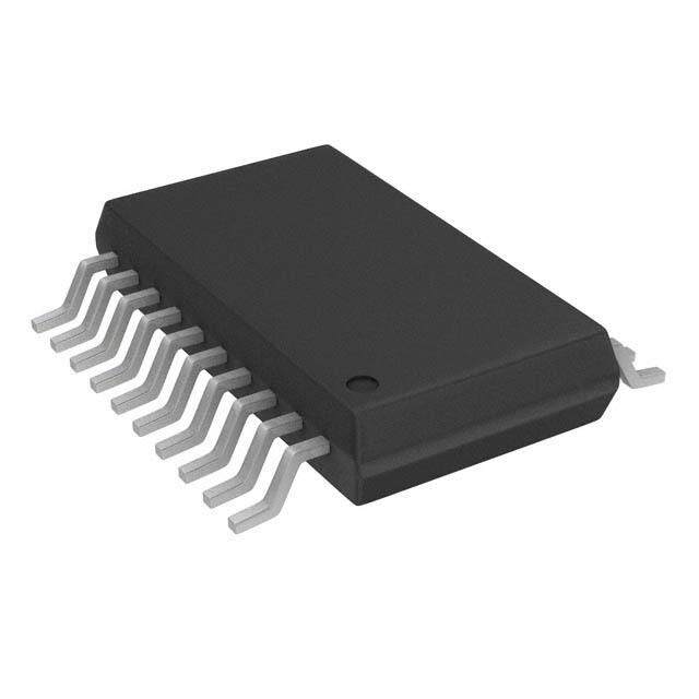
| 供应商器件封装 | 28-SOIC |
| 包装 | 管件 |
| 外设 | 欠压检测/复位,LVD,POR,PWM,WDT |
| 封装/外壳 | 28-SOIC(0.295",7.50mm 宽) |
| 工作温度 | -40°C ~ 85°C |
| 振荡器类型 | 内部 |
| 数据转换器 | A/D 5x10b |
| 标准包装 | 27 |
| 核心处理器 | PIC |
| 核心尺寸 | 8-位 |
| 电压-电源(Vcc/Vdd) | 4.2 V ~ 5.5 V |
| 程序存储器类型 | 闪存 |
| 程序存储容量 | 24KB(12K x 16) |
| 连接性 | I²C, SPI, UART/USART |
| 速度 | 40MHz |


- 商务部:美国ITC正式对集成电路等产品启动337调查
- 曝三星4nm工艺存在良率问题 高通将骁龙8 Gen1或转产台积电
- 太阳诱电将投资9.5亿元在常州建新厂生产MLCC 预计2023年完工
- 英特尔发布欧洲新工厂建设计划 深化IDM 2.0 战略
- 台积电先进制程称霸业界 有大客户加持明年业绩稳了
- 达到5530亿美元!SIA预计今年全球半导体销售额将创下新高
- 英特尔拟将自动驾驶子公司Mobileye上市 估值或超500亿美元
- 三星加码芯片和SET,合并消费电子和移动部门,撤换高东真等 CEO
- 三星电子宣布重大人事变动 还合并消费电子和移动部门
- 海关总署:前11个月进口集成电路产品价值2.52万亿元 增长14.8%


PDF Datasheet 数据手册内容提取
PIC18FXX39 Enhanced FLASH Microcontrollers with Single Phase Induction Motor Control Kernel High Performance RISC CPU: Peripheral Features: • Linear program memory addressing to 24 Kbytes • High current sink/source 25mA/25mA • Linear data memory addressing to 1.4 Kbytes • Three external interrupt pins • 20 MHz operation (5 MIPs): • Timer0 module: 8-bit/16-bit timer/counter with - 20MHz oscillator/clock input 8-bit programmable prescaler - 5MHz oscillator/clock input with PLL active • Timer1 module: 16-bit timer/counter • Timer3 module: 16-bit timer/counter • 16-bit wide instructions, 8-bit wide data path • Secondary oscillator clock option - Timer1/Timer3 • 8 x 8 Single Cycle Hardware Multiplier • Two PWM modules: Special Microcontroller Features: - Resolution is 1- to 10-bit, • 100,000 erase/write cycle Enhanced FLASH Max. PWM freq. @ 8-bit resolution = 156kHz program memory typical 10-bit resolution = 39kHz • 1,000,000 erase/write cycle Data EEPROM memory • Single Phase Induction Motor Control kernel • FLASH/Data EEPROM Retention: > 100 years - Programmable Motor Control Technology • Power-on Reset (POR), Power-up Timer (PWRT) (ProMPT™) provides open loop Variable and Oscillator Start-up Timer (OST) Frequency (VF) control • Programmable code protection - User programmable Voltage vs. Frequency • Power saving SLEEP mode curve • Single supply 5V In-Circuit Serial Programming™ - Most suitable for shaded pole and permanent (ICSP™) via two pins split capacitor type motors • In-Circuit Debug (ICD) via two pins • Master Synchronous Serial Port (MSSP) module with two modes of operation: Analog Features: - 3-wire SPI (supports all 4 SPI modes) • Compatible 10-bit Analog-to-Digital Converter - I2C™ Master and Slave mode module (A/D) with: • Addressable USART module: - Fast sampling rate - Supports RS-485 and RS-232 - Conversion available during SLEEP • Parallel Slave Port (PSP) module - DNL = ±1LSb, INL = ±1LSb • Programmable Low Voltage Detection (PLVD) CMOS Technology: - Supports interrupt on Low Voltage Detection • Low power, high speed FLASH/EEPROM • Programmable Brown-out Reset (BOR) technology • Fully static design • Wide operating voltage range (2.0V to 5.5V) • Industrial and Extended temperature ranges Program Memory Data Memory MSSP I/O 10-bit PWM Timers Device SRAM EEPROM Master AUSART Bytes Words Pins A/D (ch) 10-bit SPI 16-bit/WDT (Bytes) (Bytes) I2C PIC18F2439 12K 6144 640 256 21 5 2 Yes Yes Yes 3/1 PIC18F2539 24K 12288 1408 256 21 5 2 Yes Yes Yes 3/1 PIC18F4439 12K 6144 640 256 32 8 2 Yes Yes Yes 3/1 PIC18F4539 24K 12288 1408 256 32 8 2 Yes Yes Yes 3/1 Preliminary 2002-2013 Microchip Technology Inc. DS30485B-page 1
PIC18FXX39 Pin Diagrams 44-Pin TQFP X/CKDODI/SDASP3SP2SP1SP0CK/SCL TSSPPPPS12 C6/C5/C4/D3/D2/D1/D0/C3/WMWMC RRRRRRRRPPN 43210987654 44444333333 RC7/RX/DT 1 33 NC RD4/PSP4 2 32 RC0/T13CKI RD5/PSP5 3 31 OSC2/CLKO/RA6 RD6/PSP6 4 30 OSC1/CLKI RD7/PSP7 5 PIC18F4439 29 VSS VSS 6 28 VDD VDD 7 PIC18F4539 27 RE2/AN7/CS RB0/INT0 8 26 RE1/AN6/WR RB1/INT1 9 25 RE0/AN5/RD RB2/INT2 10 24 RA5/AN4/SS/LVDIN RB3 11 23 RA4/T0CKI 11111111222 23456789012 NNRRRRMRRRR CCBBBBCAAAA 45/P6/P7/PLR0/A1/A2/A3/A GGG/VNNNN MCDPP012/V3/V RR EE FF -+ 44-Pin QFN C6/TX/CKC5/SDOC4/SDI/SDAD3/PSP3D2/PSP2D1/PSP1D0/PSP0C3/SCK/SCLWM2WM1C0/T13CKI RRRRRRRRPPR 43210987654 RC7/RX/DT 1 4444433333333 OSC2/CLKO/RA6 RD4/PSP4 2 32 OSC1/CLKI RD5/PSP5 3 31 VSS RD6/PSP6 4 30 AVSS RD7/PSP7 5 PIC18F4439 29 VDD VSS 6 PIC18F4539 28 VDD VDD 7 27 RE2/AN7/CS AVDD 8 26 RE1/AN6/WR RB0/INT0 9 25 RE0/AN5/RD RB1/INT1 10 24 RA5/AN4/SS/LVDIN RB2/INT2 11 23 RA4/T0CKI 11111111222 23456789012 RNRRRRMRRRR BCBBBBCAAAA 3 45/P6/P7/PLR0/A1/A2/A3/A GMGCGD/VPPN0N1N2/VN3/V -REF+REF Preliminary DS30485B-page 2 2002-2013 Microchip Technology Inc.
PIC18FXX39 Pin Diagrams (Cont.’d) 40-Pin DIP MCLR/VPP 1 40 RB7/PGD RA0/AN0 2 39 RB6/PGC RA1/AN1 3 38 RB5/PGM RA2/AN2/VREF- 4 37 RB4 RA3/AN3/VREF+ 5 36 RB3 RA4/T0CKI 6 35 RB2/INT2 RA5/AN4/SS/LVDIN 7 34 RB1/INT1 9 9 RE0/AN5/RD 8 3 3 33 RB0/INT0 RE1/AN6/WR 9 44 45 32 VDD RE2/AN7/CS 10 F F 31 VSS VDD 11 18 18 30 RD7/PSP7 VSS 12 C C 29 RD6/PSP6 OSC1/CLKI 13 PI PI 28 RD5/PSP5 OSC2/CLKO/RA6 14 27 RD4/PSP4 RC0/T13CKI 15 26 RC7/RX/DT PWM2 16 25 RC6/TX/CK PWM1 17 24 RC5/SDO RC3/SCK/SCL 18 23 RC4/SDI/SDA RD0/PSP0 19 22 RD3/PSP3 RD1/PSP1 20 21 RD2/PSP2 28-Pin DIP, SOIC MCLR/VPP 1 28 RB7/PGD RA0/AN0 2 27 RB6/PGC RA1/AN1 3 26 RB5/PGM RA2/AN2/VREF- 4 25 RB4 RA3/AN3/VREF+ 5 39 39 24 RB3 RA4/T0CKI 6 24 25 23 RB2/INT2 RA5/AN4/SS/LVDIN 7 F F 22 RB1/INT1 VSS 8 18 18 21 RB0/INT0 OSC1/CLKI 9 C C 20 VDD OSC2/CLKO/RA6 10 PI PI 19 VSS RC0/T13CKI 11 18 RC7/RX/DT PWM2 12 17 RC6/TX/CK PWM1 13 16 RC5/SDO RC3/SCK/SCL 14 15 RC4/SDI/SDA Preliminary 2002-2013 Microchip Technology Inc. DS30485B-page 3
PIC18FXX39 Table of Contents 1.0 Device Overview..........................................................................................................................................................................7 2.0 Oscillator Configurations............................................................................................................................................................19 3.0 Reset..........................................................................................................................................................................................23 4.0 Memory Organization.................................................................................................................................................................33 5.0 FLASH Program Memory...........................................................................................................................................................51 6.0 Data EEPROM Memory.............................................................................................................................................................61 7.0 8 X 8 Hardware Multiplier...........................................................................................................................................................67 8.0 Interrupts....................................................................................................................................................................................69 9.0 I/O Ports.....................................................................................................................................................................................83 10.0 Timer0 Module...........................................................................................................................................................................99 11.0 Timer1 Module.........................................................................................................................................................................103 12.0 Timer2 Module.........................................................................................................................................................................107 13.0 Timer3 Module.........................................................................................................................................................................109 14.0 Single Phase Induction Motor Control Kernel..........................................................................................................................113 15.0 Pulse Width Modulation (PWM) Modules.................................................................................................................................123 16.0 Master Synchronous Serial Port (MSSP) Module....................................................................................................................125 17.0 Addressable Universal Synchronous Asynchronous Receiver Transmitter (USART)..............................................................165 18.0 Compatible 10-bit Analog-to-Digital Converter (A/D) Module...................................................................................................181 19.0 Low Voltage Detect..................................................................................................................................................................189 20.0 Special Features of the CPU....................................................................................................................................................195 21.0 Instruction Set Summary..........................................................................................................................................................211 22.0 Development Support...............................................................................................................................................................253 23.0 Electrical Characteristics..........................................................................................................................................................259 24.0 DC and AC Characteristics Graphs and Tables.......................................................................................................................287 25.0 Packaging Information..............................................................................................................................................................297 Appendix A: Revision History.............................................................................................................................................................305 Appendix B: Device Differences.........................................................................................................................................................305 Appendix C: Conversion Considerations...........................................................................................................................................306 Appendix D: Migration from High-End to Enhanced Devices.............................................................................................................307 Index..................................................................................................................................................................................................309 On-Line Support.................................................................................................................................................................................317 Systems Information and Upgrade Hot Line......................................................................................................................................317 Reader Response..............................................................................................................................................................................318 PIC18FXX39 Product Identification System.......................................................................................................................................319 Preliminary DS30485B-page 4 2002-2013 Microchip Technology Inc.
PIC18FXX39 TO OUR VALUED CUSTOMERS It is our intention to provide our valued customers with the best documentation possible to ensure successful use of your Microchip products. To this end, we will continue to improve our publications to better suit your needs. Our publications will be refined and enhanced as new volumes and updates are introduced. If you have any questions or comments regarding this publication, please contact the Marketing Communications Department via E-mail at docerrors@mail.microchip.com or fax the Reader Response Form in the back of this data sheet to (480) 792-4150. We welcome your feedback. Most Current Data Sheet To obtain the most up-to-date version of this data sheet, please register at our Worldwide Web site at: http://www.microchip.com You can determine the version of a data sheet by examining its literature number found on the bottom outside corner of any page. The last character of the literature number is the version number, (e.g., DS30000A is version A of document DS30000). Errata An errata sheet, describing minor operational differences from the data sheet and recommended workarounds, may exist for current devices. As device/documentation issues become known to us, we will publish an errata sheet. The errata will specify the revision of silicon and revision of document to which it applies. To determine if an errata sheet exists for a particular device, please check with one of the following: • Microchip’s Worldwide Web site; http://www.microchip.com • Your local Microchip sales office (see last page) • The Microchip Corporate Literature Center; U.S. FAX: (480) 792-7277 When contacting a sales office or the literature center, please specify which device, revision of silicon and data sheet (include liter- ature number) you are using. Customer Notification System Register on our web site at www.microchip.com/cn to receive the most current information on all of our products. Preliminary 2002-2013 Microchip Technology Inc. DS30485B-page 5
PIC18FXX39 NOTES: Preliminary DS30485B-page 6 2002-2013 Microchip Technology Inc.
PIC18FXX39 1.0 DEVICE OVERVIEW 1.2 Details on Individual Family Members This document contains device specific information for the following devices: Devices in the PIC18FXX39 family are available in 28-pin (PIC18F2X39) and 40/44-pin (PIC18F4X39) • PIC18F2439 • PIC18F4439 packages. Block diagrams for the two groups are • PIC18F2539 • PIC18F4539 shown in Figure1-1 and Figure1-2. This family offers the advantages of all PIC18 micro- The devices are differentiated from each other in four controllers - namely, high computational performance ways: at an economical price - with the addition of high-endur- 1. FLASH program memory and data RAM ance Enhanced FLASH program memory. The (12Kbytes and 640bytes for PIC18FX439 PIC18FXX39 family also provides an off-the-shelf solu- devices, 24Kbytes and 1408bytes for tion for simple motor control applications, allowing PIC18FX539) users to create speed control solutions with small part 2. A/D channels (5 for PIC18F2X39 devices, 8 for counts and short development times. PIC18F4X39) 1.1 Key Features 3. I/O ports (3 ports on PIC18F2X39, 5 ports on PIC18F4X39 devices) 1.1.1 PROGRAMMABLE MOTOR 4. Parallel Slave Port (present only on PROCESSOR TECHNOLOGY PIC18F4X39 devices) (ProMPT™) MOTOR CONTROL All other features for devices in this family are identical. The integrated motor control kernel uses on-chip Pulse These are summarized in Table1-1. Width Modulation (PWM) to provide speed control for The pinouts for all devices are listed in Table1-2 and single phase induction motors. Through a convenient Table1-3. set of Application Program Interfaces (APIs) and vari- able frequency technology for open loop control, users can develop applications with little or no previous expe- rience in motor control techniques. ProMPT motor con- trol provides modulated output over a range of 0 to 127Hz, and has a pre-defined V/F curve that can be reprogrammed to suit the application. 1.1.2 OTHER PIC18FXX39 FEATURES • Memory Endurance: The Enhanced FLASH cells for both program memory and data EEPROM are rated to last for many thousands of erase/write cycles - up to 100,000 for program memory, and 1,000,000 for EEPROM. Data retention without refresh is conservatively estimated to be greater than 100 years at 25°C. • Self-programmability: These devices can write to their own program memory spaces under internal software control. By using a bootloader routine located in the protected Boot Block at the top of pro- gram memory, it becomes possible to create an application that can update itself in the field. • Addressable USART: This serial communication module is capable of standard RS-232 operation using the internal oscillator block, removing the need for an external crystal (and its accompanying power requirement) in applications that talk to the outside world. • 10-bit A/D Converter: This module offers up to 8conversion channels for flexibility in sensor monitoring and control, as well as the ability to do conversions while the device is in SLEEP mode. Preliminary 2002-2013 Microchip Technology Inc. DS30485B-page 7
PIC18FXX39 TABLE 1-1: PIC18FXX39 DEVICE FEATURES Features PIC18F2439 PIC18F2539 PIC18F4439 PIC18F4539 Operating Frequency DC - 40 MHz DC - 40 MHz DC - 40 MHz DC - 40 MHz Program Memory (Bytes) 12K 24K 12K 24K Program Memory (Instructions) 6144 12288 6144 12288 Data Memory (Bytes) 640 1408 640 1408 Data EEPROM Memory (Bytes) 256 256 256 256 Interrupt Sources 15 15 16 16 I/O Ports Ports A, B, C Ports A, B, C Ports A, B, C, D, E Ports A, B, C, D, E Timers 3 3 3 3 PWM Modules(1) 2 2 2 2 Single Phase Induction Yes Yes Yes Yes Motor Control MSSP, MSSP, MSSP, MSSP, Serial Communications Addressable Addressable Addressable Addressable USART USART USART USART Parallel Communications — — PSP PSP 10-bit Analog-to-Digital Module 5 input channels 5 input channels 8 input channels 8 input channels POR, BOR, POR, BOR, POR, BOR, POR, BOR, RESET Instruction, RESET Instruction, RESET Instruction, RESET Instruction, RESETS (and Delays) Stack Full, Stack Full, Stack Full, Stack Full, Stack Underflow Stack Underflow Stack Underflow Stack Underflow (PWRT, OST) (PWRT, OST) (PWRT, OST) (PWRT, OST) Programmable Low Voltage Yes Yes Yes Yes Detect Programmable Brown-out Reset Yes Yes Yes Yes Instruction Set 75 Instructions 75 Instructions 75 Instructions 75 Instructions 40-pin DIP 40-pin DIP 28-pin DIP 28-pin DIP Packages 44-pin TQFP 44-pin TQFP 28-pin SOIC 28-pin SOIC 44-pin QFN 44-pin QFN Note 1: PWM modules are used exclusively in conjunction with the motor control kernel, and are not available for other applications. Preliminary DS30485B-page 8 2002-2013 Microchip Technology Inc.
PIC18FXX39 FIGURE 1-1: PIC18F2X39 BLOCK DIAGRAM Data Bus<8> PORTA 21 Table Pointer Data Latch RA0/AN0 8 8 8 Data RAM RA1/AN1 21 inc/dec logic RA2/AN2/VREF- RA3/AN3/VREF+ Address Latch RA4/T0CKI Address Latch 21 PCLATU PCLATH 12(2) RA5/AN4/SS/LVDIN RA6 Program Memory Address<12> (up to 2 Mbytes) PCU PCH PCL Program Counter 4 12 4 Data Latch BSR FSR0 Bank0, F 31 Level Stack FSR1 FSR2 12 PORTB 16 inc/dec Table Latch Decode logic RB0/INT0 RB1/INT1 RB2/INT2 8 ROM Latch RB3 RB4 RB5/PGM RB6/PGC Instruction Register RB7/PGD 8 Instruction Decode & Control PRODH PRODL OSC2/CLKO OSC1/CLKI 3 8 x 8 Multiply Power-up 8 Timer T1OSCI Timing Oscillator BIT OP WREG PORTC T1OSCO Generation Start-up Timer 8 8 8 RC0/T13CKI Power-on RC3/SCK/SCL Reset 8 RC4/SDI/SDA 4X PLL Watchdog RC5/SDO Timer ALU<8> RC6/TX/CK RC7/RX/DT Brown-out Precision 8 Reset Voltage Reference Low Voltage MCLR Programming In-Circuit PWM1 VDD, VSS Debugger PWM2 Timer0 Timer1 Timer2 Timer3 A/D Converter Master Addressable PWM1 PWM2 Synchronous Data EEPROM USART Serial Port Note 1: The high order bits of the Direct Address for the RAM are from the BSR register (except for the MOVFF instruction). 2: Many of the general purpose I/O pins are multiplexed with one or more peripheral module functions. The multiplexing combinations are device dependent. Preliminary 2002-2013 Microchip Technology Inc. DS30485B-page 9
PIC18FXX39 FIGURE 1-2: PIC18F4X39 BLOCK DIAGRAM Data Bus<8> PORTA RA0/AN0 Table Pointer Data Latch RA1/AN1 21 RA2/AN2/VREF- 8 8 8 D(uapta t oR 4AKM RA3/AN3/VREF+ 21 inc/dec logic address reach) RA4/T0CKI RA5/AN4/SS/LVDIN Address Latch RA6 Address Latch 21 PCLAT U PCLATH 12(2) Program Memory Address<12> PORTB (up to 2 Mbytes) PCU PCH PCL RB0/INT0 Data Latch Program Counter 4 12 4 RB1/INT1 BSR FSR0 Bank0, F RB2/INT2 31 Level Stack FSR1 RB3 FSR2 RB4 12 RB5/PGM RB6/PGC 16 inc/dec RB7/PGD Decode logic Table Latch PORTC 8 ROM Latch RC0/T13CKI RC3/SCK/SCL RC4/SDI/SDA Instruction RC5/SDO Register RC6/TX/CK RC7/RX/DT 8 Instruction Decode & Control PRODH PRODL OSC2/CLKO PORTD OSC1/CLKI 3 8 x 8 Multiply RD0/PSP0 Power-up 8 RD1/PSP1 Timer RD2/PSP2 T1OSCI Timing Oscillator BIT OP WREG RD3/PSP3 T1OSCO Generation Start-up Timer 8 8 8 RD4/PSP4 Power-on RD5/PSP5 Reset RD6/PSP6 8 RD7/PSP7 4X PLL Watchdog ALU<8> Timer PORTE Brown-out Precision 8 Reset Voltage RE0/AN5/RD Reference Low Voltage MCLR Programming RE1/AN6/WR RE2/AN7/CS In-Circuit VDD, VSS Debugger PWM1 PWM2 Timer0 Timer1 Timer2 Timer3 A/D Converter Master PWM1 PWM2 Synchronous Addressable Parallel Slave Port Data EEPROM USART Serial Port Note 1: The high order bits of the Direct Address for the RAM are from the BSR register (except for the MOVFF instruction). 2: Many of the general purpose I/O pins are multiplexed with one or more peripheral module functions. The multiplexing combinations are device dependent. Preliminary DS30485B-page 10 2002-2013 Microchip Technology Inc.
PIC18FXX39 TABLE 1-2: PIC18F2X39 PINOUT I/O DESCRIPTIONS Pin Number Pin Buffer Pin Name Description Type Type DIP SOIC MCLR/VPP 1 1 Master Clear (input) or high voltage ICSP programming enable pin. MCLR I ST Master Clear (Reset) input. This pin is an active low RESET to the device. VPP I ST High voltage ICSP programming enable pin. NC — — — — These pins should be left unconnected. OSC1/CLKI 9 9 Oscillator crystal or external clock input. OSC1 I CMOS Oscillator crystal input or external clock source input. CLKI I CMOS External clock source input. Always associated with pin function OSC1. (See related OSC1/CLKI, OSC2/CLKO pins.) OSC2/CLKO/RA6 10 10 Oscillator crystal or clock output. OSC2 O — Oscillator crystal output. Connects to crystal or resonator in Crystal Oscillator mode. CLKO O — In EC mode, OSC2 pin outputs CLKO which has 1/4 the frequency of OSC1, and denotes the instruction cycle rate. RA6 I/O TTL General purpose I/O pin. PORTA is a bi-directional I/O port. RA0/AN0 2 2 RA0 I/O TTL Digital I/O. AN0 I Analog Analog input 0. RA1/AN1 3 3 RA1 I/O TTL Digital I/O. AN1 I Analog Analog input 1. RA2/AN2/VREF- 4 4 RA2 I/O TTL Digital I/O. AN2 I Analog Analog input 2. VREF- I Analog A/D Reference Voltage (Low) input. RA3/AN3/VREF+ 5 5 RA3 I/O TTL Digital I/O. AN3 I Analog Analog input 3. VREF+ I Analog A/D Reference Voltage (High) input. RA4/T0CKI 6 6 RA4 I/O ST/OD Digital I/O. Open drain when configured as output. T0CKI I ST Timer0 external clock input. RA5/AN4/SS/LVDIN 7 7 RA5 I/O TTL Digital I/O. AN4 I Analog Analog input 4. SS I ST SPI Slave Select input. LVDIN I Analog Low Voltage Detect input. RA6 See the OSC2/CLKO/RA6 pin. Legend: TTL = TTL compatible input CMOS= CMOS compatible input or output ST = Schmitt Trigger input with CMOS levels I = Input O = Output P = Power OD = Open Drain (no P diode to VDD) Preliminary 2002-2013 Microchip Technology Inc. DS30485B-page 11
PIC18FXX39 TABLE 1-2: PIC18F2X39 PINOUT I/O DESCRIPTIONS (CONTINUED) Pin Number Pin Buffer Pin Name Description Type Type DIP SOIC PORTB is a bi-directional I/O port. PORTB can be software programmed for internal weak pull-ups on all inputs. RB0/INT0 21 21 RB0 I/O TTL Digital I/O. INT0 I ST External interrupt 0. RB1/INT1 22 22 RB1 I/O TTL Digital I/O. INT1 I ST External interrupt 1. RB2/INT2 23 23 RB2 I/O TTL Digital I/O. INT2 I ST External interrupt 2. RB3 24 24 I/O TTL Digital I/O. RB4 25 25 I/O TTL Digital I/O. Interrupt-on-change pin. RB5/PGM 26 26 RB5 I/O TTL Digital I/O. Interrupt-on-change pin. PGM I/O ST Low Voltage ICSP programming enable pin. RB6/PGC 27 27 RB6 I/O TTL Digital I/O. Interrupt-on-change pin. PGC I/O ST In-Circuit Debugger and ICSP programming clock pin. RB7/PGD 28 28 RB7 I/O TTL Digital I/O. Interrupt-on-change pin. PGD I/O ST In-Circuit Debugger and ICSP programming data pin. Legend: TTL = TTL compatible input CMOS= CMOS compatible input or output ST = Schmitt Trigger input with CMOS levels I = Input O = Output P = Power OD = Open Drain (no P diode to VDD) Preliminary DS30485B-page 12 2002-2013 Microchip Technology Inc.
PIC18FXX39 TABLE 1-2: PIC18F2X39 PINOUT I/O DESCRIPTIONS (CONTINUED) Pin Number Pin Buffer Pin Name Description Type Type DIP SOIC PORTC is a bi-directional I/O port. RC0/T13CKI 11 11 RC0 I/O ST Digital I/O. T13CKI I ST Timer1/Timer3 external clock input. RC3/SCK/SCL 14 14 RC3 I/O ST Digital I/O. SCK I/O ST Synchronous serial clock input/output for SPI mode. SCL I/O ST Synchronous serial clock input/output for I2C mode. RC4/SDI/SDA 15 15 RC4 I/O ST Digital I/O. SDI I ST SPI Data in. SDA I/O ST I2C Data I/O. RC5/SDO 16 16 RC5 I/O ST Digital I/O. SDO O — SPI Data out. RC6/TX/CK 17 17 RC6 I/O ST Digital I/O. TX O — USART Asynchronous Transmit. CK I/O ST USART Synchronous Clock (see related RX/DT). RC7/RX/DT 18 18 RC7 I/O ST Digital I/O. RX I ST USART Asynchronous Receive. DT I/O ST USART Synchronous Data (see related TX/CK). PWM1 13 13 O — PWM Channel 1 (motor control) output. PWM2 12 12 O — PWM Channel 2 (motor control) output. VSS 8, 19 8, 19 P — Ground reference for logic and I/O pins. VDD 20 20 P — Positive supply for logic and I/O pins. Legend: TTL = TTL compatible input CMOS= CMOS compatible input or output ST = Schmitt Trigger input with CMOS levels I = Input O = Output P = Power OD = Open Drain (no P diode to VDD) Preliminary 2002-2013 Microchip Technology Inc. DS30485B-page 13
PIC18FXX39 TABLE 1-3: PIC18F4X39 PINOUT I/O DESCRIPTIONS Pin Number Pin Buffer Pin Name Description Type Type DIP QFN TQFP MCLR/VPP 1 18 18 Master Clear (input) or high voltage ICSP programming enable pin. MCLR I ST Master Clear (Reset) input. This pin is an active low RESET to the device. VPP I ST High voltage ICSP programming enable pin. OSC1/CLKI 13 32 30 Oscillator crystal or external clock input. OSC1 I CMOS Oscillator crystal input or external clock source input. CLKI I CMOS External clock source input. Always associated with pin function OSC1. (See related OSC1/CLKI, OSC2/CLKO pins.) OSC2/CLKO/RA6 14 33 31 Oscillator crystal or clock output. OSC2 O — Oscillator crystal output. Connects to crystal or resonator in Crystal Oscillator mode. CLKO O — In EC mode, OSC2 pin outputs CLKO, which has 1/4 the frequency of OSC1 and denotes the instruction cycle rate. RA6 I/O TTL General purpose I/O pin. PORTA is a bi-directional I/O port. RA0/AN0 2 19 19 RA0 I/O TTL Digital I/O. AN0 I Analog Analog input 0. RA1/AN1 3 20 20 RA1 I/O TTL Digital I/O. AN1 I Analog Analog input 1. RA2/AN2/VREF- 4 21 21 RA2 I/O TTL Digital I/O. AN2 I Analog Analog input 2. VREF- I Analog A/D Reference Voltage (Low) input. RA3/AN3/VREF+ 5 22 22 RA3 I/O TTL Digital I/O. AN3 I Analog Analog input 3. VREF+ I Analog A/D Reference Voltage (High) input. RA4/T0CKI 6 23 23 RA4 I/O ST/OD Digital I/O. Open drain when configured as output. T0CKI I ST Timer0 external clock input. RA5/AN4/SS/LVDIN 7 24 24 RA5 I/O TTL Digital I/O. AN4 I Analog Analog input 4. SS I ST SPI Slave Select input. LVDIN I Analog Low Voltage Detect input. RA6 (See the OSC2/CLKO/RA6 pin.) Legend: TTL = TTL compatible input CMOS = CMOS compatible input or output ST = Schmitt Trigger input with CMOS levels I = Input O = Output P = Power OD = Open Drain (no P diode to VDD) Preliminary DS30485B-page 14 2002-2013 Microchip Technology Inc.
PIC18FXX39 TABLE 1-3: PIC18F4X39 PINOUT I/O DESCRIPTIONS (CONTINUED) Pin Number Pin Buffer Pin Name Description Type Type DIP QFN TQFP PORTB is a bi-directional I/O port. PORTB can be software programmed for internal weak pull-ups on all inputs. RB0/INT0 33 9 8 RB0 I/O TTL Digital I/O. INT0 I ST External interrupt 0. RB1/INT1 34 10 9 RB1 I/O TTL Digital I/O. INT1 I ST External interrupt 1. RB2/INT2 35 11 10 RB2 I/O TTL Digital I/O. INT2 I ST External interrupt 2. RB3 36 12 11 I/O TTL Digital I/O. RB4 37 14 14 I/O TTL Digital I/O. Interrupt-on-change pin. RB5/PGM 38 15 15 RB5 I/O TTL Digital I/O. Interrupt-on-change pin. PGM I/O ST Low Voltage ICSP programming enable pin. RB6/PGC 39 16 16 RB6 I/O TTL Digital I/O. Interrupt-on-change pin. PGC I/O ST In-Circuit Debugger and ICSP programming clock pin. RB7/PGD 40 17 17 RB7 I/O TTL Digital I/O. Interrupt-on-change pin. PGD I/O ST In-Circuit Debugger and ICSP programming data pin. Legend: TTL = TTL compatible input CMOS = CMOS compatible input or output ST = Schmitt Trigger input with CMOS levels I = Input O = Output P = Power OD = Open Drain (no P diode to VDD) Preliminary 2002-2013 Microchip Technology Inc. DS30485B-page 15
PIC18FXX39 TABLE 1-3: PIC18F4X39 PINOUT I/O DESCRIPTIONS (CONTINUED) Pin Number Pin Buffer Pin Name Description Type Type DIP QFN TQFP PORTC is a bi-directional I/O port. RC0/T13CKI 15 34 32 RC0 I/O ST Digital I/O. T13CKI I ST Timer1/Timer3 external clock input. RC3/SCK/SCL 18 37 37 RC3 I/O ST Digital I/O. SCK I/O ST Synchronous serial clock input/output for SPI mode. SCL I/O ST Synchronous serial clock input/output for I2C mode. RC4/SDI/SDA 23 42 42 RC4 I/O ST Digital I/O. SDI I ST SPI Data in. SDA I/O ST I2C Data I/O. RC5/SDO 24 43 43 RC5 I/O ST Digital I/O. SDO O — SPI Data out. RC6/TX/CK 25 44 44 RC6 I/O ST Digital I/O. TX O — USART Asynchronous Transmit. CK I/O ST USART Synchronous Clock (see related RX/DT). RC7/RX/DT 26 1 1 RC7 I/O ST Digital I/O. RX I ST USART Asynchronous Receive. DT I/O ST USART Synchronous Data (see related TX/CK). PWM1 17 35 36 O — PWM Channel 1 (motor control) output. PWM2 16 36 35 O — PWM Channel 2 (motor control) output. Legend: TTL = TTL compatible input CMOS = CMOS compatible input or output ST = Schmitt Trigger input with CMOS levels I = Input O = Output P = Power OD = Open Drain (no P diode to VDD) Preliminary DS30485B-page 16 2002-2013 Microchip Technology Inc.
PIC18FXX39 TABLE 1-3: PIC18F4X39 PINOUT I/O DESCRIPTIONS (CONTINUED) Pin Number Pin Buffer Pin Name Description Type Type DIP QFN TQFP PORTD is a bi-directional I/O port, or a Parallel Slave Port (PSP) for interfacing to a microprocessor port. These pins have TTL input buffers when PSP module is enabled. RD0/PSP0 19 38 38 I/O RD0 ST Digital I/O. PSP0 TTL Parallel Slave Port Data. RD1/PSP1 20 39 39 I/O RD1 ST Digital I/O. PSP1 TTL Parallel Slave Port Data. RD2/PSP2 21 40 40 I/O RD2 ST Digital I/O. PSP2 TTL Parallel Slave Port Data. RD3/PSP3 22 41 41 I/O RD3 ST Digital I/O. PSP3 TTL Parallel Slave Port Data. RD4/PSP4 27 2 2 I/O RD4 ST Digital I/O. PSP4 TTL Parallel Slave Port Data. RD5/PSP5 28 3 3 I/O RD5 ST Digital I/O. PSP5 TTL Parallel Slave Port Data. RD6/PSP6 29 4 4 I/O RD6 ST Digital I/O. PSP6 TTL Parallel Slave Port Data. RD7/PSP7 30 5 5 I/O RD7 ST Digital I/O. PSP7 TTL Parallel Slave Port Data. Legend: TTL = TTL compatible input CMOS = CMOS compatible input or output ST = Schmitt Trigger input with CMOS levels I = Input O = Output P = Power OD = Open Drain (no P diode to VDD) Preliminary 2002-2013 Microchip Technology Inc. DS30485B-page 17
PIC18FXX39 TABLE 1-3: PIC18F4X39 PINOUT I/O DESCRIPTIONS (CONTINUED) Pin Number Pin Buffer Pin Name Description Type Type DIP QFN TQFP PORTE is a bi-directional I/O port. RE0/RD/AN5 8 25 25 I/O RE0 ST Digital I/O. RD TTL Read control for parallel slave port (see also WR and CS pins). AN5 Analog Analog input 5. RE1/WR/AN6 9 26 26 I/O RE1 ST Digital I/O. WR TTL Write control for parallel slave port (see CS and RD pins). AN6 Analog Analog input 6. RE2/CS/AN7 10 27 27 I/O RE2 ST Digital I/O. CS TTL Chip Select control for parallel slave port (see related RD and WR). AN7 Analog Analog input 7. VSS 12, 31 6, 31 6, 29 P — Ground reference for logic and I/O pins. VDD 11, 32 7, 28, 7, 28 P — Positive supply for logic and I/O pins. 29 AVSS — 30 — P — Ground reference for analog modules. AVDD — 8 — P — Positive supply for analog modules. NC — 13 12, 13, — — These pins should be left unconnected. 33, 34 Legend: TTL = TTL compatible input CMOS = CMOS compatible input or output ST = Schmitt Trigger input with CMOS levels I = Input O = Output P = Power OD = Open Drain (no P diode to VDD) Preliminary DS30485B-page 18 2002-2013 Microchip Technology Inc.
PIC18FXX39 2.0 OSCILLATOR FIGURE 2-1: CRYSTAL/CERAMIC CONFIGURATIONS RESONATOR OPERATION (HS CONFIGURATION) 2.1 Oscillator Types C1(1) OSC1 The PIC18FXX39 can be operated in four different To Oscillator modes at a frequency of 20 MHz. The user Internal can program three configuration bits (FOSC2, FOSC1, XTAL RF(3) Logic and FOSC0) to select one of these four modes: SLEEP 1. HS High Speed Crystal/Resonator RS(2) 2. HS + PLL High Speed Crystal/Resonator C2(1) OSC2 PIC18FXX39 with PLL enabled using 5 MHz crystal Note 1: See Table2-1 for recommended values of C1 and C2. 3. EC External Clock 2: A series resistor (RS) may be required for 4. ECIO External Clock with I/O pin AT strip cut crystals. enabled 3: RF varies with the Oscillator mode chosen. Note: The operation of the Motor Control kernel and its APIs (Section14.0) is based on an An external clock source may also be connected to the assumed clock frequency of 20MHz. OSC1 pin in the HS mode, as shown in Figure2-2. Changing the oscillator frequency will change the timing used in the Motor Con- FIGURE 2-2: EXTERNAL CLOCK INPUT trol kernel accordingly. To achieve the best OPERATION (HS OSC results in motor control applications, a CONFIGURATION) clock frequency of 20MHz is highly recommended. Clock from OSC1 2.2 Crystal Oscillator/Ceramic Ext. System PIC18FXX39 Resonators Open OSC2 In HS or HS+PLL Oscillator modes, a crystal or ceramic resonator is connected to the OSC1 and OSC2 pins to establish oscillation. Figure2-1 shows the pin connections. Note 1: Higher capacitance increases the stability The PIC18FXX39 oscillator design requires the use of of the oscillator, but also increases the a parallel cut crystal. start-up time. Note: Use of a series cut crystal may give a fre- 2: Since each resonator/crystal has its own quency out of the crystal manufacturers characteristics, the user should consult the specifications. resonator/crystal manufacturer for appro- priate values of external components, or verify oscillator performance. Preliminary 2002-2013 Microchip Technology Inc. DS30485B-page 19
PIC18FXX39 TABLE 2-1: CAPACITOR SELECTION FOR FIGURE 2-3: EXTERNAL CLOCK INPUT CRYSTAL OSCILLATOR OPERATION (EC CONFIGURATION) Ranges Tested: Mode Freq C1 C2 Clock from OSC1 HS 20.0 MHz 15-33 pF 15-33 pF Ext. System PIC18FXX39 These values are for design guidance only. FOSC/4 OSC2 See notes following this table. Crystals Used The ECIO Oscillator mode functions like the EC mode, 20.0 MHz Epson CA-301 20.000M-C ± 30 PPM except that the OSC2 pin becomes an additional gen- eral purpose I/O pin. The I/O pin becomes bit 6 of PORTA (RA6). Figure2-4 shows the pin connections Note 1: Higher capacitance increases the stability for the ECIO Oscillator mode. of the oscillator, but also increases the start-up time. FIGURE 2-4: EXTERNAL CLOCK INPUT OPERATION 2: Rs may be required in HS mode to avoid (ECIO CONFIGURATION) overdriving crystals with low drive level specification. 3: Since each resonator/crystal has its own Clock from OSC1 characteristics, the user should consult the Ext. System PIC18FXX39 resonator/crystal manufacturer for appro- RA6 I/O (OSC2) priate values of external components, or verify oscillator performance. 2.4 HS/PLL 2.3 External Clock Input A Phase Locked Loop circuit is provided as a program- mable option for users that want to multiply the fre- The EC and ECIO Oscillator modes require an external quency of the incoming crystal oscillator signal by 4. clock source to be connected to the OSC1 pin. The For an input clock frequency of 5 MHz, the internal feedback device between OSC1 and OSC2 is turned clock frequency will be multiplied to 20 MHz. This is off in these modes to save current. There is no oscilla- useful for customers who are concerned with EMI due tor start-up time required after a Power-on Reset or to high frequency crystals. after a recovery from SLEEP mode. The PLL can only be enabled when the oscillator con- In the EC Oscillator mode, the oscillator frequency figuration bits are programmed for HS mode. If they are divided by 4 is available on the OSC2 pin. This signal programmed for any other mode, the PLL is not may be used for test purposes or to synchronize other enabled and the system clock will come directly from logic. Figure2-3 shows the pin connections for the EC OSC1. Oscillator mode. The PLL is one of the modes specified by the FOSC<2:0> configuration bits. The Oscillator mode is specified during device programming. A PLL lock timer is used to ensure that the PLL has locked before device execution starts. The PLL lock timer has a time-out that is called TPLL. Preliminary DS30485B-page 20 2002-2013 Microchip Technology Inc.
PIC18FXX39 FIGURE 2-5: PLL BLOCK DIAGRAM HS Osc (from Configuration bit Register) PLL Enable Phase OSC2 Comparator FIN Loop Crystal VCO Filter Osc FOUT SYSCLK X U M OSC1 4 2.5 Effects of SLEEP Mode on the The first timer is the Power-up Timer (PWRT), which On-Chip Oscillator optionally provides a fixed delay of 72 ms (nominal) on power-up only (POR and BOR). The second timer is When the device executes a SLEEP instruction, the the Oscillator Start-up Timer (OST), intended to keep oscillator is turned off and the device is held at the the chip in RESET until the crystal oscillator is stable. beginning of an instruction cycle (Q1 state). With the With the PLL enabled (HS/PLL Oscillator mode), the oscillator off, the OSC1 and OSC2 signals will stop time-out sequence following a Power-on Reset is differ- oscillating. Since all the transistor switching currents ent from other Oscillator modes. The time-out have been removed, SLEEP mode achieves the lowest sequence is as follows: current consumption of the device (only leakage cur- rents). Enabling any on-chip feature that will operate 1. The PWRT time-out is invoked after a POR time during SLEEP will increase the current consumed dur- delay has expired. ing SLEEP. The user can wake from SLEEP through 2. The Oscillator Start-up Timer (OST) is invoked. external RESET, Watchdog Timer Reset, or through an However, this is still not a sufficient amount of interrupt. time to allow the PLL to lock at high frequencies. 3. The PWRT timer is used to provide an additional 2.6 Power-up Delays fixed 2 ms (nominal) time-out to allow the PLL ample time to lock to the incoming clock Power-up delays are controlled by two timers, so that frequency. no external RESET circuitry is required for most appli- cations. The delays ensure that the device is kept in RESET, until the device power supply and clock are stable. For additional information on RESET operation, see Section3.0. TABLE 2-2: OSC1 AND OSC2 PIN STATES IN SLEEP MODE OSC Mode OSC1 Pin OSC2 Pin ECIO Floating Configured as PORTA, bit 6 EC Floating At logic low HS Feedback inverter disabled, at quiescent Feedback inverter disabled, at quiescent voltage level voltage level Note: See Table3-1 in the “Reset” section, for time-outs due to SLEEP and MCLR Reset. Preliminary 2002-2013 Microchip Technology Inc. DS30485B-page 21
PIC18FXX39 NOTES: Preliminary DS30485B-page 22 2002-2013 Microchip Technology Inc.
PIC18FXX39 3.0 RESET Most registers are not affected by a WDT wake-up, since this is viewed as the resumption of normal oper- The PIC18FXX39 differentiates between various kinds ation. Status bits from the RCON register, RI, TO, PD, of RESET: POR and BOR, are set or cleared differently in different a) Power-on Reset (POR) RESET situations, as indicated in Table3-2. These bits are used in software to determine the nature of the b) MCLR Reset during normal operation RESET. See Table3-3 for a full description of the c) MCLR Reset during SLEEP RESET states of all registers. d) Watchdog Timer (WDT) Reset (during normal A simplified block diagram of the On-Chip Reset Circuit operation) is shown in Figure3-1. e) Programmable Brown-out Reset (BOR) The Enhanced MCU devices have a MCLR noise filter f) RESET Instruction in the MCLR Reset path. The filter will detect and g) Stack Full Reset ignore small pulses. h) Stack Underflow Reset The MCLR pin is not driven low by any internal Most registers are unaffected by a RESET. Their status RESETS, including the WDT. is unknown on POR and unchanged by all other RESETS. The other registers are forced to a “RESET state” on Power-on Reset, MCLR, WDT Reset, Brown- out Reset, MCLR Reset during SLEEP and by the RESET instruction. FIGURE 3-1: SIMPLIFIED BLOCK DIAGRAM OF ON-CHIP RESET CIRCUIT RESET Instruction Stack Pointer Stack Full/Underflow Reset External Reset MCLR SLEEP WDT WDT Module Time-out Reset VDD Rise Detect Power-on Reset VDD Brown-out Reset BOREN S OST/PWRT OST Chip_Reset 10-bit Ripple Counter R Q OSC1 PWRT On-chip RC OSC(1) 10-bit Ripple Counter Enable PWRT Enable OST(2) Note 1: This is a separate oscillator from the RC oscillator of the CLKI pin. 2: See Table3-1 for time-out situations. Preliminary 2002-2013 Microchip Technology Inc. DS30485B-page 23
PIC18FXX39 3.1 Power-on Reset (POR) 3.3 Oscillator Start-up Timer (OST) A Power-on Reset pulse is generated on-chip when The Oscillator Start-up Timer (OST) provides a 1024 VDD rise is detected. To take advantage of the POR cir- oscillator cycle (from OSC1 input) delay after the cuitry, just tie the MCLR pin directly (or through a resis- PWRT delay is over (parameter32). This ensures that tor) to VDD. This will eliminate external RC components the crystal oscillator or resonator has started and usually needed to create a Power-on Reset delay. A stabilized. minimum rise rate for VDD is specified The OST time-out is invoked only for XT, LP and HS (parameterD004). For a slow rise time, see Figure3-2. modes and only on Power-on Reset or wake-up from When the device starts normal operation (i.e., exits the SLEEP. RESET condition), device operating parameters (volt- age, frequency, temperature, etc.) must be met to 3.4 PLL Lock Time-out ensure operation. If these conditions are not met, the With the PLL enabled, the time-out sequence following device must be held in RESET until the operating a Power-on Reset is different from other Oscillator conditions are met. modes. A portion of the Power-up Timer is used to pro- vide a fixed time-out that is sufficient for the PLL to lock FIGURE 3-2: EXTERNAL POWER-ON to the main oscillator frequency. This PLL lock time-out RESET CIRCUIT (FOR (TPLL) is typically 2 ms and follows the Oscillator SLOW VDD POWER-UP) Start-up Time-out (OST). 3.5 Brown-out Reset (BOR) VDD A configuration bit, BOREN, can disable (if clear/ D R programmed), or enable (if set) the Brown-out Reset R1 circuitry. If VDD falls below parameterD005 for greater MCLR than parameter35, the brown-out situation will reset C PIC18FXXXX the chip. A RESET may not occur if VDD falls below parameterD005 for less than parameter35. The chip will remain in Brown-out Reset until VDD rises above BVDD. If the Power-up Timer is enabled, it will be invoked after VDD rises above BVDD; it then will keep the chip in RESET for an additional time delay Note 1: External Power-on Reset circuit is required only if the VDD power-up slope is too slow. (parameter33). If VDD drops below BVDD while the The diode D helps discharge the capacitor Power-up Timer is running, the chip will go back into a quickly when VDD powers down. Brown-out Reset and the Power-up Timer will be initial- 2: R < 40 k is recommended to make sure that ized. Once VDD rises above BVDD, the Power-up Timer the voltage drop across R does not violate will execute the additional time delay. the device’s electrical specification. 3.6 Time-out Sequence 3: R1 = 100 to 1 k will limit any current flow- ing into MCLR from external capacitor C, in On power-up, the time-out sequence is as follows: the event of MCLR/VPP pin breakdown due to First, PWRT time-out is invoked after the POR time Electrostatic Discharge (ESD) or Electrical delay has expired. Then, OST is activated. The total Overstress (EOS). time-out will vary based on oscillator configuration and the status of the PWRT. For example, in RC mode with 3.2 Power-up Timer (PWRT) the PWRT disabled, there will be no time-out at all. Figure3-3, Figure3-4, Figure3-5, Figure3-6 and The Power-up Timer provides a fixed nominal time-out Figure3-7 depict time-out sequences on power-up. (parameter33) only on power-up from the POR. The Power-up Timer operates on an internal RC oscillator. Since the time-outs occur from the POR pulse, if MCLR The chip is kept in RESET as long as the PWRT is is kept low long enough, the time-outs will expire. active. The PWRT’s time delay allows VDD to rise to an Bringing MCLR high will begin execution immediately acceptable level. A configuration bit is provided to (Figure3-5). This is useful for testing purposes or to enable/disable the PWRT. synchronize more than one PIC18FXXX device operating in parallel. The power-up time delay will vary from chip-to-chip due to VDD, temperature and process variation. See DC Table3-2 shows the RESET conditions for some parameterD033 for details. Special Function Registers, while Table3-3 shows the RESET conditions for all the registers. Preliminary DS30485B-page 24 2002-2013 Microchip Technology Inc.
PIC18FXX39 TABLE 3-1: TIME-OUT IN VARIOUS SITUATIONS Power-up(2) Wake-up from Oscillator Brown-out SLEEP or Configuration PWRTE = 0 PWRTE = 1 Oscillator Switch HS with PLL enabled(1) 72 ms + 1024 TOSC 1024 TOSC 72 ms(2) + 1024 TOSC 1024 TOSC + 2 ms + 2ms + 2 ms + 2ms HS, XT, LP 72 ms + 1024 TOSC 1024 TOSC 72 ms(2) + 1024 TOSC 1024 TOSC EC 72 ms — 72 ms(2) — External RC 72 ms — 72 ms(2) — Note 1: 2 ms is the nominal time required for the 4x PLL to lock. 2: 72 ms is the nominal power-up timer delay, if implemented. REGISTER 3-1: RCON REGISTER BITS AND POSITIONS R/W-0 U-0 U-0 R/W-1 R-1 R-1 R/W-0 R/W-0 IPEN — — RI TO PD POR BOR bit 7 bit 0 Note 1: Refer to Section4.14 (page 50) for bit definitions. TABLE 3-2: STATUS BITS, THEIR SIGNIFICANCE AND THE INITIALIZATION CONDITION FOR RCON REGISTER Program RCON Condition RI TO PD POR BOR STKFUL STKUNF Counter Register Power-on Reset 0000h 0--1 1100 1 1 1 0 0 u u MCLR Reset during normal 0000h 0--u uuuu u u u u u u u operation Software Reset during normal 0000h 0--0 uuuu 0 u u u u u u operation Stack Full Reset during normal 0000h 0--u uu11 u u u u u u 1 operation Stack Underflow Reset during 0000h 0--u uu11 u u u u u 1 u normal operation MCLR Reset during SLEEP 0000h 0--u 10uu u 1 0 u u u u WDT Reset 0000h 0--u 01uu 1 0 1 u u u u WDT Wake-up PC + 2 u--u 00uu u 0 0 u u u u Brown-out Reset 0000h 0--1 11u0 1 1 1 1 0 u u Interrupt wake-up from SLEEP PC + 2(1) u--u 00uu u 1 0 u u u u Legend: u = unchanged, x = unknown, - = unimplemented bit, read as '0' Note 1: When the wake-up is due to an interrupt and the GIEH or GIEL bits are set, the PC is loaded with the interrupt vector (0x000008h or 0x000018h). Preliminary 2002-2013 Microchip Technology Inc. DS30485B-page 25
PIC18FXX39 TABLE 3-3: INITIALIZATION CONDITIONS FOR ALL REGISTERS MCLR Resets Power-on Reset, WDT Reset Wake-up via WDT Register Applicable Devices Brown-out Reset RESET Instruction or Interrupt Stack Resets TOSU 2439 4439 2539 4539 ---0 0000 ---0 0000 ---0 uuuu(1) TOSH 2439 4439 2539 4539 0000 0000 0000 0000 uuuu uuuu(1) TOSL 2439 4439 2539 4539 0000 0000 0000 0000 uuuu uuuu(1) STKPTR 2439 4439 2539 4539 00-0 0000 uu-0 0000 uu-u uuuu(1) PCLATU 2439 4439 2539 4539 ---0 0000 ---0 0000 ---u uuuu PCLATH 2439 4439 2539 4539 0000 0000 0000 0000 uuuu uuuu PCL 2439 4439 2539 4539 0000 0000 0000 0000 PC + 2(2) TBLPTRU 2439 4439 2539 4539 --00 0000 --00 0000 --uu uuuu TBLPTRH 2439 4439 2539 4539 0000 0000 0000 0000 uuuu uuuu TBLPTRL 2439 4439 2539 4539 0000 0000 0000 0000 uuuu uuuu TABLAT 2439 4439 2539 4539 0000 0000 0000 0000 uuuu uuuu PRODH 2439 4439 2539 4539 xxxx xxxx uuuu uuuu uuuu uuuu PRODL 2439 4439 2539 4539 xxxx xxxx uuuu uuuu uuuu uuuu INTCON 2439 4439 2539 4539 0000 000x 0000 000u uuuu uuuu(3) INTCON2 2439 4439 2539 4539 1111 -1-1 1111 -1-1 uuuu -u-u(3) INTCON3 2439 4439 2539 4539 11-0 0-00 11-0 0-00 uu-u u-uu(3) INDF0 2439 4439 2539 4539 N/A N/A N/A POSTINC0 2439 4439 2539 4539 N/A N/A N/A POSTDEC0 2439 4439 2539 4539 N/A N/A N/A PREINC0 2439 4439 2539 4539 N/A N/A N/A PLUSW0 2439 4439 2539 4539 N/A N/A N/A FSR0H 2439 4439 2539 4539 ---- xxxx ---- uuuu ---- uuuu FSR0L 2439 4439 2539 4539 xxxx xxxx uuuu uuuu uuuu uuuu WREG 2439 4439 2539 4539 xxxx xxxx uuuu uuuu uuuu uuuu INDF1 2439 4439 2539 4539 N/A N/A N/A POSTINC1 2439 4439 2539 4539 N/A N/A N/A POSTDEC1 2439 4439 2539 4539 N/A N/A N/A PREINC1 2439 4439 2539 4539 N/A N/A N/A PLUSW1 2439 4439 2539 4539 N/A N/A N/A Legend: u = unchanged, x = unknown, - = unimplemented bit, read as '0', q = value depends on condition. Shaded cells indicate conditions do not apply for the designated device. * These registers are retained to maintain compatibility with PIC18FXX2 devices; however, one or more bits are reserved. Users should not modify the value of these bits. See Section4.9.2 for details. Note 1: When the wake-up is due to an interrupt and the GIEL or GIEH bit is set, the TOSU, TOSH and TOSL are updated with the current value of the PC. The STKPTR is modified to point to the next location in the hardware stack. 2: When the wake-up is due to an interrupt and the GIEL or GIEH bit is set, the PC is loaded with the interrupt vector (0008h or 0018h). 3: One or more bits in the INTCONx or PIRx registers will be affected (to cause wake-up). 4: See Table3-2 for RESET value for specific condition. 5: Bit 6 of PORTA, LATA, and TRISA are enabled in ECIO and RCIO Oscillator modes only. In all other Oscillator modes, they are disabled and read ‘0’. 6: Bit 6 of PORTA, LATA and TRISA are not available on all devices. When unimplemented, they are read ‘0’. Preliminary DS30485B-page 26 2002-2013 Microchip Technology Inc.
PIC18FXX39 TABLE 3-3: INITIALIZATION CONDITIONS FOR ALL REGISTERS (CONTINUED) MCLR Resets Power-on Reset, WDT Reset Wake-up via WDT Register Applicable Devices Brown-out Reset RESET Instruction or Interrupt Stack Resets FSR1H 2439 4439 2539 4539 ---- xxxx ---- uuuu ---- uuuu FSR1L 2439 4439 2539 4539 xxxx xxxx uuuu uuuu uuuu uuuu BSR 2439 4439 2539 4539 ---- 0000 ---- 0000 ---- uuuu INDF2 2439 4439 2539 4539 N/A N/A N/A POSTINC2 2439 4439 2539 4539 N/A N/A N/A POSTDEC2 2439 4439 2539 4539 N/A N/A N/A PREINC2 2439 4439 2539 4539 N/A N/A N/A PLUSW2 2439 4439 2539 4539 N/A N/A N/A FSR2H 2439 4439 2539 4539 ---- xxxx ---- uuuu ---- uuuu FSR2L 2439 4439 2539 4539 xxxx xxxx uuuu uuuu uuuu uuuu STATUS 2439 4439 2539 4539 ---x xxxx ---u uuuu ---u uuuu TMR0H 2439 4439 2539 4539 0000 0000 uuuu uuuu uuuu uuuu TMR0L 2439 4439 2539 4539 xxxx xxxx uuuu uuuu uuuu uuuu T0CON 2439 4439 2539 4539 1111 1111 1111 1111 uuuu uuuu OSCCON* 2439 4439 2539 4539 ---- ---0 ---- ---0 ---- ---u LVDCON 2439 4439 2539 4539 --00 0101 --00 0101 --uu uuuu WDTCON 2439 4439 2539 4539 ---- ---0 ---- ---0 ---- ---u RCON(4) 2439 4439 2539 4539 0--q 11qq 0--q qquu u--u qquu TMR1H 2439 4439 2539 4539 xxxx xxxx uuuu uuuu uuuu uuuu TMR1L 2439 4439 2539 4539 xxxx xxxx uuuu uuuu uuuu uuuu T1CON 2439 4439 2539 4539 0-00 0000 u-uu uuuu u-uu uuuu TMR2* 2439 4439 2539 4539 0000 0000 0000 0000 uuuu uuuu PR2* 2439 4439 2539 4539 1111 1111 1111 1111 1111 1111 T2CON* 2439 4439 2539 4539 -000 0000 -000 0000 -uuu uuuu SSPBUF 2439 4439 2539 4539 xxxx xxxx uuuu uuuu uuuu uuuu SSPADD 2439 4439 2539 4539 0000 0000 0000 0000 uuuu uuuu SSPSTAT 2439 4439 2539 4539 0000 0000 0000 0000 uuuu uuuu SSPCON1 2439 4439 2539 4539 0000 0000 0000 0000 uuuu uuuu SSPCON2 2439 4439 2539 4539 0000 0000 0000 0000 uuuu uuuu Legend: u = unchanged, x = unknown, - = unimplemented bit, read as '0', q = value depends on condition. Shaded cells indicate conditions do not apply for the designated device. * These registers are retained to maintain compatibility with PIC18FXX2 devices; however, one or more bits are reserved. Users should not modify the value of these bits. See Section4.9.2 for details. Note 1: When the wake-up is due to an interrupt and the GIEL or GIEH bit is set, the TOSU, TOSH and TOSL are updated with the current value of the PC. The STKPTR is modified to point to the next location in the hardware stack. 2: When the wake-up is due to an interrupt and the GIEL or GIEH bit is set, the PC is loaded with the interrupt vector (0008h or 0018h). 3: One or more bits in the INTCONx or PIRx registers will be affected (to cause wake-up). 4: See Table3-2 for RESET value for specific condition. 5: Bit 6 of PORTA, LATA, and TRISA are enabled in ECIO and RCIO Oscillator modes only. In all other Oscillator modes, they are disabled and read ‘0’. 6: Bit 6 of PORTA, LATA and TRISA are not available on all devices. When unimplemented, they are read ‘0’. Preliminary 2002-2013 Microchip Technology Inc. DS30485B-page 27
PIC18FXX39 TABLE 3-3: INITIALIZATION CONDITIONS FOR ALL REGISTERS (CONTINUED) MCLR Resets Power-on Reset, WDT Reset Wake-up via WDT Register Applicable Devices Brown-out Reset RESET Instruction or Interrupt Stack Resets ADRESH 2439 4439 2539 4539 xxxx xxxx uuuu uuuu uuuu uuuu ADRESL 2439 4439 2539 4539 xxxx xxxx uuuu uuuu uuuu uuuu ADCON0 2439 4439 2539 4539 0000 00-0 0000 00-0 uuuu uu-u ADCON1 2439 4439 2539 4539 00-- 0000 00-- 0000 uu-- uuuu CCPR1H 2439 4439 2539 4539 xxxx xxxx uuuu uuuu uuuu uuuu CCPR1L* 2439 4439 2539 4539 xxxx xxxx uuuu uuuu uuuu uuuu CCP1CON* 2439 4439 2539 4539 --00 0000 --00 0000 --uu uuuu CCPR2H 2439 4439 2539 4539 xxxx xxxx uuuu uuuu uuuu uuuu CCPR2L* 2439 4439 2539 4539 xxxx xxxx uuuu uuuu uuuu uuuu CCP2CON* 2439 4439 2539 4539 --00 0000 --00 0000 --uu uuuu TMR3H 2439 4439 2539 4539 xxxx xxxx uuuu uuuu uuuu uuuu TMR3L 2439 4439 2539 4539 xxxx xxxx uuuu uuuu uuuu uuuu T3CON 2439 4439 2539 4539 0000 0000 uuuu uuuu uuuu uuuu SPBRG 2439 4439 2539 4539 0000 0000 0000 0000 uuuu uuuu RCREG 2439 4439 2539 4539 0000 0000 0000 0000 uuuu uuuu TXREG 2439 4439 2539 4539 0000 0000 0000 0000 uuuu uuuu TXSTA 2439 4439 2539 4539 0000 -010 0000 -010 uuuu -uuu RCSTA 2439 4439 2539 4539 0000 000x 0000 000x uuuu uuuu EEADR 2439 4439 2539 4539 0000 0000 0000 0000 uuuu uuuu EEDATA 2439 4439 2539 4539 0000 0000 0000 0000 uuuu uuuu EECON1 2439 4439 2539 4539 xx-0 x000 uu-0 u000 uu-0 u000 EECON2 2439 4439 2539 4539 ---- ---- ---- ---- ---- ---- Legend: u = unchanged, x = unknown, - = unimplemented bit, read as '0', q = value depends on condition. Shaded cells indicate conditions do not apply for the designated device. * These registers are retained to maintain compatibility with PIC18FXX2 devices; however, one or more bits are reserved. Users should not modify the value of these bits. See Section4.9.2 for details. Note 1: When the wake-up is due to an interrupt and the GIEL or GIEH bit is set, the TOSU, TOSH and TOSL are updated with the current value of the PC. The STKPTR is modified to point to the next location in the hardware stack. 2: When the wake-up is due to an interrupt and the GIEL or GIEH bit is set, the PC is loaded with the interrupt vector (0008h or 0018h). 3: One or more bits in the INTCONx or PIRx registers will be affected (to cause wake-up). 4: See Table3-2 for RESET value for specific condition. 5: Bit 6 of PORTA, LATA, and TRISA are enabled in ECIO and RCIO Oscillator modes only. In all other Oscillator modes, they are disabled and read ‘0’. 6: Bit 6 of PORTA, LATA and TRISA are not available on all devices. When unimplemented, they are read ‘0’. Preliminary DS30485B-page 28 2002-2013 Microchip Technology Inc.
PIC18FXX39 TABLE 3-3: INITIALIZATION CONDITIONS FOR ALL REGISTERS (CONTINUED) MCLR Resets Power-on Reset, WDT Reset Wake-up via WDT Register Applicable Devices Brown-out Reset RESET Instruction or Interrupt Stack Resets IPR2 2439 4439 2539 4539 ---1 1111 ---1 1111 ---u uuuu PIR2 2439 4439 2539 4539 ---0 0000 ---0 0000 ---u uuuu(3) PIE2 2439 4439 2539 4539 ---0 0000 ---0 0000 ---u uuuu 2439 4439 2539 4539 1111 1111 1111 1111 uuuu uuuu IPR1 2439 4439 2539 4539 -111 1111 -111 1111 -uuu uuuu 2439 4439 2539 4539 0000 0000 0000 0000 uuuu uuuu(3) PIR1 2439 4439 2539 4539 -000 0000 -000 0000 -uuu uuuu(3) 2439 4439 2539 4539 0000 0000 0000 0000 uuuu uuuu PIE1 2439 4439 2539 4539 -000 0000 -000 0000 -uuu uuuu TRISE 2439 4439 2539 4539 0000 -111 0000 -111 uuuu -uuu TRISD 2439 4439 2539 4539 1111 1111 1111 1111 uuuu uuuu TRISC* 2439 4439 2539 4539 1111 1111 1111 1111 uuuu uuuu TRISB 2439 4439 2539 4539 1111 1111 1111 1111 uuuu uuuu TRISA(5,6) 2439 4439 2539 4539 -111 1111(5) -111 1111(5) -uuu uuuu(5) LATE 2439 4439 2539 4539 ---- -xxx ---- -uuu ---- -uuu LATD 2439 4439 2539 4539 xxxx xxxx uuuu uuuu uuuu uuuu LATC* 2439 4439 2539 4539 xxxx xxxx uuuu uuuu uuuu uuuu LATB 2439 4439 2539 4539 xxxx xxxx uuuu uuuu uuuu uuuu LATA(5,6) 2439 4439 2539 4539 -xxx xxxx(5) -uuu uuuu(5) -uuu uuuu(5) PORTE 2439 4439 2539 4539 ---- -000 ---- -000 ---- -uuu PORTD 2439 4439 2539 4539 xxxx xxxx uuuu uuuu uuuu uuuu PORTC* 2439 4439 2539 4539 xxxx xxxx uuuu uuuu uuuu uuuu PORTB 2439 4439 2539 4539 xxxx xxxx uuuu uuuu uuuu uuuu PORTA(5,6) 2439 4439 2539 4539 -x0x 0000(5) -u0u 0000(5) -uuu uuuu(5) Legend: u = unchanged, x = unknown, - = unimplemented bit, read as '0', q = value depends on condition. Shaded cells indicate conditions do not apply for the designated device. * These registers are retained to maintain compatibility with PIC18FXX2 devices; however, one or more bits are reserved. Users should not modify the value of these bits. See Section4.9.2 for details. Note 1: When the wake-up is due to an interrupt and the GIEL or GIEH bit is set, the TOSU, TOSH and TOSL are updated with the current value of the PC. The STKPTR is modified to point to the next location in the hardware stack. 2: When the wake-up is due to an interrupt and the GIEL or GIEH bit is set, the PC is loaded with the interrupt vector (0008h or 0018h). 3: One or more bits in the INTCONx or PIRx registers will be affected (to cause wake-up). 4: See Table3-2 for RESET value for specific condition. 5: Bit 6 of PORTA, LATA, and TRISA are enabled in ECIO and RCIO Oscillator modes only. In all other Oscillator modes, they are disabled and read ‘0’. 6: Bit 6 of PORTA, LATA and TRISA are not available on all devices. When unimplemented, they are read ‘0’. Preliminary 2002-2013 Microchip Technology Inc. DS30485B-page 29
PIC18FXX39 FIGURE 3-3: TIME-OUT SEQUENCE ON POWER-UP (MCLR TIED TO VDD) VDD MCLR INTERNAL POR TPWRT PWRT TIME-OUT TOST OST TIME-OUT INTERNAL RESET FIGURE 3-4: TIME-OUT SEQUENCE ON POWER-UP (MCLR NOT TIED TO VDD): CASE 1 VDD MCLR INTERNAL POR TPWRT PWRT TIME-OUT TOST OST TIME-OUT INTERNAL RESET FIGURE 3-5: TIME-OUT SEQUENCE ON POWER-UP (MCLR NOT TIED TO VDD): CASE 2 VDD MCLR INTERNAL POR TPWRT PWRT TIME-OUT TOST OST TIME-OUT INTERNAL RESET Preliminary DS30485B-page 30 2002-2013 Microchip Technology Inc.
PIC18FXX39 FIGURE 3-6: SLOW RISE TIME (MCLR TIED TO VDD) 5V VDD 0V 1V MCLR INTERNAL POR TPWRT PWRT TIME-OUT TOST OST TIME-OUT INTERNAL RESET FIGURE 3-7: TIME-OUT SEQUENCE ON POR W/ PLL ENABLED (MCLR TIED TO VDD) VDD MCLR IINTERNAL POR TPWRT PWRT TIME-OUT TOST OST TIME-OUT TPLL PLL TIME-OUT INTERNAL RESET Note: TOST = 1024 clock cycles. TPLL 2 ms max. First three stages of the PWRT timer. Preliminary 2002-2013 Microchip Technology Inc. DS30485B-page 31
PIC18FXX39 NOTES: Preliminary DS30485B-page 32 2002-2013 Microchip Technology Inc.
PIC18FXX39 4.0 MEMORY ORGANIZATION The PIC18F2539 and PIC18F4539 each have a total of 24Kbytes, or 12K of single word instructions of FLASH There are three memory blocks in Enhanced MCU memory, from addresses 0000h to 5FFFh. The next devices. These memory blocks are: 8Kbytes beyond this space (from 6000h to 7FFFh) are • Program Memory reserved for the Motor Control kernel; accessing locations in this range will return random information. • Data RAM • Data EEPROM The PIC18F2439 and PIC18F4439 each have 12Kbytes, or 6K of single word instructions of FLASH Data and program memory use separate busses, memory, from addresses 0000h to 2FFFh. The next which allows for concurrent access of these blocks. 4Kbytes of this space (from 3000h to 3FFFh) are Additional detailed information for FLASH program reserved for the Motor Control kernel; accessing memory and Data EEPROM is provided in Section5.0 locations in this range will return random information. and Section6.0, respectively. The RESET vector address for all devices is at 0000h, and the interrupt vector addresses are at 0008h and 4.1 Program Memory Organization 0018h. A 21-bit program counter is capable of addressing the The memory maps for the PIC18FX439 and 2-Mbyte program memory space. Accessing a location PIC18FX539 devices are shown in Figure4-1. between the physically implemented memory and the top of the 2-MByte range will cause a read of all ‘0’s (a Note: The ProMPT Motor Control kernel is iden- NOP instruction). tical for all PIC18FXX39 devices, regard- less of the difference in reserved block size between PIC18FX439 and PIC18FX539 devices FIGURE 4-1: PROGRAM MEMORY MAP AND STACK FOR PIC18FXX39 DEVICES PC<20:0> CALL,RCALL,RETURN 21 RETFIE,RETLW Stack Level 1 Stack Level 31 PIC18FX439 Devices PIC18FX539 Devices RESET Vector 0000h RESET Vector 0000h High Priority Interrupt Vector 0008h High Priority Interrupt Vector 0008h Low Priority Interrupt Vector 0018h Low Priority Interrupt Vector 0018h On-Chip Program Memory On-Chip 2FFFh Program Memory 3000h Reserved e 3FFFh c a 4000h p S y or 5FFFh m e 6000h M Reserved ser U Read '0' 7FFFh 8000h Read '0' 1FFFFFh 1FFFFFh 200000h 200000h Note: Size of memory areas not to scale. Preliminary 2002-2013 Microchip Technology Inc. DS30485B-page 33
PIC18FXX39 4.2 Return Address Stack 4.2.2 RETURN STACK POINTER (STKPTR) The return address stack allows any combination of up to 31 program calls and interrupts to occur. The PC The STKPTR register contains the stack pointer value, (Program Counter) is pushed onto the stack when a the STKFUL (stack full) status bit, and the STKUNF CALL or RCALL instruction is executed, or an interrupt (stack underflow) status bits. Register4-1 shows the is acknowledged. The PC value is pulled off the stack STKPTR register. The value of the stack pointer can be on a RETURN, RETLW or a RETFIE instruction. 0 through 31. The stack pointer increments when val- PCLATU and PCLATH are not affected by any of the ues are pushed onto the stack and decrements when RETURN or CALL instructions. values are popped off the stack. At RESET, the stack pointer value will be ‘0’. The user may read and write The stack operates as a 31-word by 21-bit RAM and a the stack pointer value. This feature can be used by a 5-bit stack pointer, with the stack pointer initialized to Real-Time Operating System for return stack 00000b after all RESETS. There is no RAM associated maintenance. with stack pointer 00000b. This is only a RESET value. During a CALL type instruction, causing a push onto the After the PC is pushed onto the stack 31 times (without stack, the stack pointer is first incremented and the popping any values off the stack), the STKFUL bit is RAM location pointed to by the stack pointer is written set. The STKFUL bit can only be cleared in software or with the contents of the PC. During a RETURN type by a POR. instruction, causing a pop from the stack, the contents The action that takes place when the stack becomes of the RAM location pointed to by the STKPTR are full depends on the state of the STVREN (Stack Over- transferred to the PC and then the stack pointer is flow Reset Enable) configuration bit. Refer to decremented. Section21.0 for a description of the device configura- The stack space is not part of either program or data tion bits. If STVREN is set (default), the 31st push will space. The stack pointer is readable and writable, and push the (PC + 2) value onto the stack, set the STKFUL the address on the top of the stack is readable and writ- bit, and reset the device. The STKFUL bit will remain able through SFR registers. Data can also be pushed set and the stack pointer will be set to ‘0’. to, or popped from the stack using the top-of-stack If STVREN is cleared, the STKFUL bit will be set on the SFRs. Status bits indicate if the stack pointer is at, or 31st push and the stack pointer will increment to 31. beyond the 31 levels provided. Any additional pushes will not overwrite the 31st push, and STKPTR will remain at 31. 4.2.1 TOP-OF-STACK ACCESS When the stack has been popped enough times to The top of the stack is readable and writable. Three unload the stack, the next pop will return a value of zero register locations, TOSU, TOSH and TOSL hold the to the PC and sets the STKUNF bit, while the stack contents of the stack location pointed to by the pointer remains at ‘0’. The STKUNF bit will remain set STKPTR register. This allows users to implement a until cleared in software or a POR occurs. software stack if necessary. After a CALL, RCALL or interrupt, the software can read the pushed value by Note: Returning a value of zero to the PC on an reading the TOSU, TOSH and TOSL registers. These underflow has the effect of vectoring the values can be placed on a user defined software stack. program to the RESET vector, where the At return time, the software can replace the TOSU, stack conditions can be verified and TOSH and TOSL and do a return. appropriate actions can be taken. The user must disable the global interrupt enable bits during this time to prevent inadvertent stack operations. Preliminary DS30485B-page 34 2002-2013 Microchip Technology Inc.
PIC18FXX39 REGISTER 4-1: STKPTR REGISTER R/C-0 R/C-0 U-0 R/W-0 R/W-0 R/W-0 R/W-0 R/W-0 STKFUL STKUNF — SP4 SP3 SP2 SP1 SP0 bit 7 bit 0 bit 7(1) STKFUL: Stack Full Flag bit 1 = Stack became full or overflowed 0 = Stack has not become full or overflowed bit 6(1) STKUNF: Stack Underflow Flag bit 1 = Stack underflow occurred 0 = Stack underflow did not occur bit 5 Unimplemented: Read as '0' bit 4-0 SP4:SP0: Stack Pointer Location bits Note 1: Bit 7 and bit 6 can only be cleared in user software or by a POR. Legend: R = Readable bit W = Writable bit U = Unimplemented bit, read as ‘0’ - n = Value at POR ‘1’ = Bit is set ‘0’ = Bit is cleared x = Bit is unknown FIGURE 4-2: RETURN ADDRESS STACK AND ASSOCIATED REGISTERS Return Address Stack 11111 11110 11101 TOSU TOSH TOSL STKPTR<4:0> 0x00 0x1A 0x34 00010 00011 Top-of-Stack 0x001A34 00010 0x000D58 00001 00000 4.2.3 PUSH AND POP INSTRUCTIONS 4.2.4 STACK FULL/UNDERFLOW RESETS Since the Top-of-Stack (TOS) is readable and writable, These RESETS are enabled by programming the the ability to push values onto the stack and pull values STVREN configuration bit. When the STVREN bit is off the stack, without disturbing normal program execu- disabled, a full or underflow condition will set the appro- tion, is a desirable option. To push the current PC value priate STKFUL or STKUNF bit, but not cause a device onto the stack, a PUSH instruction can be executed. RESET. When the STVREN bit is enabled, a full or This will increment the stack pointer and load the cur- underflow condition will set the appropriate STKFUL or rent PC value onto the stack. TOSU, TOSH and TOSL STKUNF bit and then cause a device RESET. The can then be modified to place a return address on the STKFUL or STKUNF bits are only cleared by the user stack. software or a POR Reset. The ability to pull the TOS value off of the stack and replace it with the value that was previously pushed onto the stack, without disturbing normal execution, is achieved by using the POP instruction. The POP instruc- tion discards the current TOS by decrementing the stack pointer. The previous value pushed onto the stack then becomes the TOS value. Preliminary 2002-2013 Microchip Technology Inc. DS30485B-page 35
PIC18FXX39 4.3 Fast Register Stack The PC addresses bytes in the program memory. To prevent the PC from becoming misaligned with word For PIC18FXX39 devices, a “fast interrupt return” instructions, the LSB of PCL is fixed to a value of ‘0’. option is available for high priority interrupts. A single The PC increments by 2 to address sequential level Fast Register Stack is provided for the STATUS, instructions in the program memory. WREG and BSR registers; it is not readable or writable. The CALL, RCALL, GOTO and program branch When the processor vectors for an interrupt, the stack instructions write to the program counter directly. For is loaded with the current value of the corresponding these instructions, the contents of PCLATH and register. If the FAST RETURN instruction is used to PCLATU are not transferred to the program counter. return from the interrupt, the values in the registers are then loaded back into the working registers. The contents of PCLATH and PCLATU will be trans- ferred to the program counter by an operation that Note: The fast interrupt return for PIC18FXX39 writes PCL. Similarly, the upper two bytes of the pro- devices is reserved for use by the ProMPT gram counter will be transferred to PCLATH and kernel and the Timer2 match interrupt. It is PCLATU by an operation that reads PCL. This is useful not available to the user for any other for computed offsets to the PC (see Section4.8.1). interrupts or returns from subroutines. 4.5 Clocking Scheme/Instruction 4.4 PCL, PCLATH and PCLATU Cycle The program counter (PC) specifies the address of the The clock input (from OSC1) is internally divided by instruction to fetch for execution. The PC is 21-bits four to generate four non-overlapping quadrature wide. The low byte is called the PCL register. This reg- clocks, namely Q1, Q2, Q3 and Q4. Internally, the pro- ister is readable and writable. The high byte is called gram counter (PC) is incremented every Q1, the the PCH register. This register contains the PC<15:8> instruction is fetched from the program memory and bits and is not directly readable or writable. Updates to latched into the instruction register in Q4. The instruc- the PCH register may be performed through the tion is decoded and executed during the following Q1 PCLATH register. The upper byte is called PCU. This through Q4. The clocks and instruction execution flow register contains the PC<20:16> bits and is not directly are shown in Figure4-3. readable or writable. Updates to the PCU register may be performed through the PCLATU register. FIGURE 4-3: CLOCK/INSTRUCTION CYCLE Q1 Q2 Q3 Q4 Q1 Q2 Q3 Q4 Q1 Q2 Q3 Q4 OSC1 Q1 Q2 Internal Phase Q3 Clock Q4 PC PC PC+2 PC+4 OSC2/CLKO (RC mode) Execute INST (PC-2) Fetch INST (PC) Execute INST (PC) Fetch INST (PC+2) Execute INST (PC+2) Fetch INST (PC+4) Preliminary DS30485B-page 36 2002-2013 Microchip Technology Inc.
PIC18FXX39 4.6 Instruction Flow/Pipelining A fetch cycle begins with the program counter (PC) incrementing in Q1. An “Instruction Cycle” consists of four Q cycles (Q1, In the execution cycle, the fetched instruction is latched Q2, Q3 and Q4). The instruction fetch and execute are into the “Instruction Register” (IR) in cycle Q1. This pipelined such that fetch takes one instruction cycle, instruction is then decoded and executed during the while decode and execute takes another instruction Q2, Q3, and Q4 cycles. Data memory is read during Q2 cycle. However, due to the pipelining, each instruction (operand read) and written during Q4 (destination effectively executes in one cycle. If an instruction write). causes the program counter to change (e.g., GOTO), then two cycles are required to complete the instruction (Example4-1). EXAMPLE 4-1: INSTRUCTION PIPELINE FLOW TCY0 TCY1 TCY2 TCY3 TCY4 TCY5 1. MOVLW 55h Fetch 1 Execute 1 2. MOVWF PORTB Fetch 2 Execute 2 3. BRA SUB_1 Fetch 3 Execute 3 4. BSF PORTA, BIT3 (Forced NOP) Fetch 4 Flush (NOP) 5. Instruction @ address SUB_1 Fetch SUB_1 Execute SUB_1 All instructions are single cycle, except for any program branches. These take two cycles since the fetch instruction is “flushed” from the pipeline while the new instruction is being fetched and then executed. 4.7 Instructions in Program Memory The CALL and GOTO instructions have an absolute pro- gram memory address embedded into the instruction. The program memory is addressed in bytes. Instruc- Since instructions are always stored on word bound- tions are stored as two bytes or four bytes in program aries, the data contained in the instruction is a word memory. The Least Significant Byte of an instruction address. The word address is written to PC<20:1>, word is always stored in a program memory location which accesses the desired byte address in program with an even address (LSB = 0). Figure4-4 shows an memory. Instruction #2 in Figure4-4 shows how the example of how instruction words are stored in the pro- instruction, ‘GOTO 000006h’, is encoded in the pro- gram memory. To maintain alignment with instruction gram memory. Program branch instructions, which boundaries, the PC increments in steps of 2 and the encode a relative address offset, operate in the same LSB will always read ‘0’ (see Section4.4). manner. The offset value stored in a branch instruction represents the number of single word instructions that the PC will be offset by. Section21.0 provides further details of the instruction set. FIGURE 4-4: INSTRUCTIONS IN PROGRAM MEMORY Word Address LSB = 1 LSB = 0 Program Memory 000000h Byte Locations 000002h 000004h 000006h Instruction 1: MOVLW 055h 0Fh 55h 000008h Instruction 2: GOTO 000006h EFh 03h 00000Ah F0h 00h 00000Ch Instruction 3: MOVFF 123h, 456h C1h 23h 00000Eh F4h 56h 000010h 000012h 000014h Preliminary 2002-2013 Microchip Technology Inc. DS30485B-page 37
PIC18FXX39 4.7.1 TWO-WORD INSTRUCTIONS second word of the instruction is executed by itself (first word was skipped), it will execute as a NOP. This action The PIC18FXX39 devices have four two-word instruc- is necessary when the two-word instruction is preceded tions: MOVFF, CALL, GOTO and LFSR. The second by a conditional instruction that changes the PC. A pro- word of these instructions has the 4 MSBs set to ‘1’s gram example that demonstrates this concept is shown and is a special kind of NOP instruction. The lower 12 in Example4-2. Refer to Section21.0 for further details bits of the second word contain data to be used by the of the instruction set. instruction. If the first word of the instruction is exe- cuted, the data in the second word is accessed. If the EXAMPLE 4-2: TWO-WORD INSTRUCTIONS CASE 1: Object Code Source Code 0110 0110 0000 0000 TSTFSZ REG1 ; is RAM location 0? 1100 0001 0010 0011 MOVFF REG1, REG2 ; No, execute 2-word instruction 1111 0100 0101 0110 ; 2nd operand holds address of REG2 0010 0100 0000 0000 ADDWF REG3 ; continue code CASE 2: Object Code Source Code 0110 0110 0000 0000 TSTFSZ REG1 ; is RAM location 0? 1100 0001 0010 0011 MOVFF REG1, REG2 ; Yes 1111 0100 0101 0110 ; 2nd operand becomes NOP 0010 0100 0000 0000 ADDWF REG3 ; continue code 4.8 Lookup Tables 4.8.2 TABLE READS/TABLE WRITES Lookup tables are implemented two ways. These are: A better method of storing data in program memory allows 2 bytes of data to be stored in each instruction • Computed GOTO location. • Table Reads Lookup table data may be stored 2 bytes per program 4.8.1 COMPUTED GOTO word by using table reads and writes. The table pointer (TBLPTR) specifies the byte address and the table A computed GOTO is accomplished by adding an offset latch (TABLAT) contains the data that is read from, or to the program counter (ADDWF PCL). written to program memory. Data is transferred to/from A lookup table can be formed with an ADDWF PCL program memory, one byte at a time. instruction and a group of RETLW 0xnn instructions. A description of the Table Read/Table Write operation WREG is loaded with an offset into the table before is shown in Section5.1. executing a call to that table. The first instruction of the called routine is the ADDWF PCL instruction. The next instruction executed will be one of the RETLW 0xnn instructions, that returns the value 0xnn to the calling function. The offset value (value in WREG) specifies the number of bytes that the program counter should advance. In this method, only one data byte may be stored in each instruction location and room on the return address stack is required. Note: The ADDWF PCL instruction does not update PCLATH and PCLATU. A read operation on PCL must be performed to update PCLATH and PCLATU. Preliminary DS30485B-page 38 2002-2013 Microchip Technology Inc.
PIC18FXX39 4.9 Data Memory Organization 4.9.1 GENERAL PURPOSE REGISTER FILE The data memory is implemented as static RAM. Each register in the data memory has a 12-bit address, The register file can be accessed either directly or indi- allowing up to 4096 bytes of data memory. The data rectly. Indirect addressing operates using a File Select memory map is divided into 16 banks that contain 256 Register and corresponding Indirect File Operand. The bytes each. The lower 4 bits of the Bank Select Regis- operation of indirect addressing is shown in ter (BSR<3:0>) select which bank will be accessed. Section4.12. The upper 4 bits for the BSR are not implemented. Enhanced MCU devices may have banked memory in The data memory contains Special Function Registers the GPR area. GPRs are not initialized by a Power-on (SFRs) and General Purpose Registers (GPRs). The Reset and are unchanged on all other RESETS. SFRs are used for control and status of the controller Data RAM is available for use as GPR registers by all and peripheral functions, while GPRs are used for data instructions. The top half of Bank 15 (F80h to FFFh) storage and scratch pad operations in the user’s appli- contains SFRs. All other banks of data memory contain cation. The SFRs start at the last location of Bank 15 GPR registers, starting with Bank 0. (FFFh) and extend downwards. Any remaining space beyond the SFRs in the Bank may be implemented as 4.9.2 SPECIAL FUNCTION REGISTERS GPRs. GPRs start at the first location of Bank 0 and grow upwards. Any read of an unimplemented location The Special Function Registers (SFRs) are registers will read as ‘0’s. used by the CPU and Peripheral Modules for control- ling the desired operation of the device. These regis- The organization of the data memory space for these ters are implemented as static RAM. A list of these devices is shown in Figure4-5 and Figure4-6. registers is given in Table4-1 and Table4-2. PIC18FX439 devices have 640bytes of data RAM, extending from Bank 0 to Bank 2 (000h through 27Fh). The SFRs can be classified into two sets; those asso- The block of 128bytes above this to the top of the bank ciated with the “core” function and those related to the (280h to 2FFh) is used as data memory for the Motor peripheral functions. Those registers related to the Control kernel, and is not available to the user. Reading “core” are described in this section, while those related these locations will return random information that to the operation of the peripheral features are reflects the kernel’s “scratch” data. Modifying the data described in the section of that peripheral feature. in these locations may disrupt the operation of the The SFRs are typically distributed among the ProMPT kernel. peripherals whose functions they control. The unused PIC18FX539 devices have 1408bytes of data RAM, SFR locations will be unimplemented and read as '0's. extending from Bank 0 to Bank 5 (000h through 57Fh). See Table4-1 for addresses for the SFRs. As with the PIC18FX439 devices, the block of 128bytes above this to the end of the bank (580h to Note: In this chapter and throughout this docu- 5FFh) is used by the Motor Control kernel. ment, certain SFR names and individual The entire data memory may be accessed directly or bits are marked with an asterisk (*). This indirectly. Direct addressing may require the use of the denotes registers that are not implemented BSR register. Indirect addressing requires the use of a in PIC18FXX39 devices, but whose names File Select Register (FSRn) and a corresponding Indi- are retained to maintain compatibility with rect File Operand (INDFn). Each FSR holds a 12-bit PIC18FXX2 devices. The designated bits address value that can be used to access any location within these registers are reserved and in the Data Memory map without banking. may be used by certain modules or the The instruction set and architecture allow operations Motor Control kernel. Users should not across all banks. This may be accomplished by indirect write to these registers or alter these bit addressing, or by the use of the MOVFF instruction. The values. Failure to do this may result in MOVFF instruction is a two-word/two-cycle instruction erratic microcontroller operation. that moves a value from one register to another. To ensure that commonly used registers (SFRs and select GPRs) can be accessed in a single cycle, regardless of the current BSR values, an Access Bank is implemented. A segment of Bank 0 and a segment of Bank 15 comprise the Access RAM. Section4.10 provides a detailed description of the Access RAM. Preliminary 2002-2013 Microchip Technology Inc. DS30485B-page 39
PIC18FXX39 FIGURE 4-5: DATA MEMORY MAP FOR PIC18FX439 BSR<3:0> Data Memory Map 000h = 0000 00h Access RAM 07Fh Bank 0 080h GPR FFh 0FFh = 0001 00h 100h Bank 1 GPR FFh 1FFh = 0010 00h GPR 200h Bank 2 27Fh 280h ProMPT Memory FFh 2FFh = 0011 300h Access Bank 00h Access RAM Low 7Fh Bank 3 Access RAM High 80h to ReUandu s‘0e0dh’ (SFRs) FFh Bank 14 When a = 0, the BSR is ignored and the Access Bank is used. The first 128 bytes are General Purpose RAM (from Bank 0). The second 128 bytes are = 1110 Special Function Registers EFFh (from Bank 15). F00h 00h = 1111 Unused Bank 15 F7Fh F80h FFh SFR FFFh When a = 1, the BSR is used to specify the RAM location that the instruction uses. Preliminary DS30485B-page 40 2002-2013 Microchip Technology Inc.
PIC18FXX39 FIGURE 4-6: DATA MEMORY MAP FOR PIC18FX539 BSR<3:0> Data Memory Map 000h = 0000 00h Access RAM 07Fh Bank 0 080h GPR FFh 0FFh 00h 100h = 0001 Bank 1 GPR FFh 1FFh 200h = 0010 00h Bank 2 GPR FFh 2FFh = 0011 00h 300h Bank 3 GPR FFh 3FFh 400h = 0100 Bank 4 GPR Access Bank 4FFh 00h = 0101 00h GPR 500h Access RAM Low 7Fh Bank 5 Access RAM High 80h FFh ProMPT Memory 5FFh (SFRs) 600h FFh = 0110 When a = 0, Bank 6 the BSR is ignored and the Unused to Read ‘00h’ Access Bank is used. Bank 14 The first 128 bytes are General Purpose RAM (from Bank 0). The second 128 bytes are = 1110 Special Function Registers EFFh (from Bank 15). 00h F00h = 1111 Unused F7Fh Bank 15 F80h FFh SFR FFFh When a = 1, the BSR is used to specify the RAM location that the instruction uses. Preliminary 2002-2013 Microchip Technology Inc. DS30485B-page 41
PIC18FXX39 TABLE 4-1: SPECIAL FUNCTION REGISTER MAP Address Name Address Name Address Name Address Name FFFh TOSU FDFh INDF2(3) FBFh CCPR1H F9Fh IPR1 FFEh TOSH FDEh POSTINC2(3) FBEh CCPR1L* F9Eh PIR1 FFDh TOSL FDDh POSTDEC2(3) FBDh CCP1CON* F9Dh PIE1 FFCh STKPTR FDCh PREINC2(3) FBCh CCPR2H F9Ch — FFBh PCLATU FDBh PLUSW2(3) FBBh CCPR2L* F9Bh — FFAh PCLATH FDAh FSR2H FBAh CCP2CON* F9Ah — FF9h PCL FD9h FSR2L FB9h — F99h — FF8h TBLPTRU FD8h STATUS FB8h — F98h — FF7h TBLPTRH FD7h TMR0H FB7h — F97h — FF6h TBLPTRL FD6h TMR0L FB6h — F96h TRISE(2) FF5h TABLAT FD5h T0CON FB5h — F95h TRISD(2) FF4h PRODH FD4h — FB4h — F94h TRISC(4) FF3h PRODL FD3h OSCCON* FB3h TMR3H F93h TRISB FF2h INTCON FD2h LVDCON FB2h TMR3L F92h TRISA FF1h INTCON2 FD1h WDTCON FB1h T3CON F91h — FF0h INTCON3 FD0h RCON FB0h — F90h — FEFh INDF0(3) FCFh TMR1H FAFh SPBRG F8Fh — FEEh POSTINC0(3) FCEh TMR1L FAEh RCREG F8Eh — FEDh POSTDEC0(3) FCDh T1CON FADh TXREG F8Dh LATE(2) FECh PREINC0(3) FCCh TMR2* FACh TXSTA F8Ch LATD(2) FEBh PLUSW0(3) FCBh PR2* FABh RCSTA F8Bh LATC(4) FEAh FSR0H FCAh T2CON* FAAh — F8Ah LATB FE9h FSR0L FC9h SSPBUF FA9h EEADR F89h LATA FE8h WREG FC8h SSPADD FA8h EEDATA F88h — FE7h INDF1(3) FC7h SSPSTAT FA7h EECON2 F87h — FE6h POSTINC1(3) FC6h SSPCON1 FA6h EECON1 F86h — FE5h POSTDEC1(3) FC5h SSPCON2 FA5h — F85h — FE4h PREINC1(3) FC4h ADRESH FA4h — F84h PORTE(2) FE3h PLUSW1(3) FC3h ADRESL FA3h — F83h PORTD(2) FE2h FSR1H FC2h ADCON0 FA2h IPR2 F82h PORTC(4) FE1h FSR1L FC1h ADCON1 FA1h PIR2 F81h PORTB FE0h BSR FC0h — FA0h PIE2 F80h PORTA * These registers are retained to maintain compatibility with PIC18FXX2 devices; however, one or more bits are reserved in PIC18FXX39 devices. Users should not alter the values of these bits. Note 1: Unimplemented registers are read as ‘0’. 2: This register is not available on PIC18F2X39 devices. 3: This is not a physical register. 4: Bits 1 and 2 are reserved; users should not alter their values. Preliminary DS30485B-page 42 2002-2013 Microchip Technology Inc.
PIC18FXX39 TABLE 4-2: REGISTER FILE SUMMARY Value on Details File Name Bit 7 Bit 6 Bit 5 Bit 4 Bit 3 Bit 2 Bit 1 Bit 0 POR, BOR on page: TOSU — — — Top-of-Stack Upper Byte (TOS<20:16>) ---0 0000 26, 34 TOSH Top-of-Stack High Byte (TOS<15:8>) 0000 0000 26, 34 TOSL Top-of-Stack Low Byte (TOS<7:0>) 0000 0000 26, 34 STKPTR STKFUL STKUNF — Return Stack Pointer 00-0 0000 26, 35 PCLATU — — — Holding Register for PC<20:16> ---0 0000 26, 36 PCLATH Holding Register for PC<15:8> 0000 0000 26, 36 PCL PC Low Byte (PC<7:0>) 0000 0000 26, 36 TBLPTRU — — bit21(2) Program Memory Table Pointer Upper Byte (TBLPTR<20:16>) --00 0000 26, 54 TBLPTRH Program Memory Table Pointer High Byte (TBLPTR<15:8>) 0000 0000 26, 54 TBLPTRL Program Memory Table Pointer Low Byte (TBLPTR<7:0>) 0000 0000 26, 54 TABLAT Program Memory Table Latch 0000 0000 26, 54 PRODH Product Register High Byte xxxx xxxx 26, 67 PRODL Product Register Low Byte xxxx xxxx 26, 67 INTCON GIE/GIEH PEIE/GIEL TMR0IE INT0IE RBIE TMR0IF INT0IF RBIF 0000 000x 26, 71 INTCON2 RBPU INTEDG0 INTEDG1 INTEDG2 — TMR0IP — RBIP 1111 -1-1 26, 72 INTCON3 INT2IP INT1IP — INT2IE INT1IE — INT2IF INT1IF 11-0 0-00 26, 73 INDF0 Uses contents of FSR0 to address data memory - value of FSR0 not changed (not a physical register) n/a 26, 47 POSTINC0 Uses contents of FSR0 to address data memory - value of FSR0 post-incremented (not a physical register) n/a 26, 47 POSTDEC0 Uses contents of FSR0 to address data memory - value of FSR0 post-decremented (not a physical register) n/a 26, 47 PREINC0 Uses contents of FSR0 to address data memory - value of FSR0 pre-incremented (not a physical register) n/a 26, 47 PLUSW0 Uses contents of FSR0 to address data memory - value of FSR0 (not a physical register). n/a 26, 47 Offset by value in WREG. FSR0H — — — — Indirect Data Memory Address Pointer 0 High Byte ---- 0000 26, 47 FSR0L Indirect Data Memory Address Pointer 0 Low Byte xxxx xxxx 26, 47 WREG Working Register xxxx xxxx 26 INDF1 Uses contents of FSR1 to address data memory - value of FSR1 not changed (not a physical register) n/a 26, 47 POSTINC1 Uses contents of FSR1 to address data memory - value of FSR1 post-incremented (not a physical register) n/a 26, 47 POSTDEC1 Uses contents of FSR1 to address data memory - value of FSR1 post-decremented (not a physical register) n/a 26, 47 PREINC1 Uses contents of FSR1 to address data memory - value of FSR1 pre-incremented (not a physical register) n/a 26, 47 PLUSW1 Uses contents of FSR1 to address data memory - value of FSR1 (not a physical register). n/a 26, 47 Offset by value in WREG. FSR1H — — — — Indirect Data Memory Address Pointer 1 High Byte ---- 0000 27, 47 FSR1L Indirect Data Memory Address Pointer 1 Low Byte xxxx xxxx 27, 47 BSR — — — — Bank Select Register ---- 0000 27, 46 INDF2 Uses contents of FSR2 to address data memory - value of FSR2 not changed (not a physical register) n/a 27, 47 POSTINC2 Uses contents of FSR2 to address data memory - value of FSR2 post-incremented (not a physical register) n/a 27, 47 POSTDEC2 Uses contents of FSR2 to address data memory - value of FSR2 post-decremented (not a physical register) n/a 27, 47 PREINC2 Uses contents of FSR2 to address data memory - value of FSR2 pre-incremented (not a physical register) n/a 27, 47 PLUSW2 Uses contents of FSR2 to address data memory - value of FSR2 (not a physical register). n/a 27, 47 Offset by value in WREG. FSR2H — — — — Indirect Data Memory Address Pointer 2 High Byte ---- 0000 27, 47 FSR2L Indirect Data Memory Address Pointer 2 Low Byte xxxx xxxx 27, 47 STATUS — — — N OV Z DC C ---x xxxx 27, 49 Legend: x = unknown, u = unchanged, - = unimplemented, q = value depends on condition * These registers (or individual bits) are retained to maintain compatibility with PIC18FXX2 devices; however, the indicated bits are reserved in PIC18FXX39 devices. Users should not alter the values of these bits. See Section4.9.2 for details. Note 1: RA6 and associated bits are configured as port pins in RCIO and ECIO Oscillator mode only and read '0' in all other Oscillator modes. 2: Bit 21 of the TBLPTRU allows access to the device configuration bits. 3: These registers and bits are reserved on the PIC18F2X39 devices; always maintain these clear. Preliminary 2002-2013 Microchip Technology Inc. DS30485B-page 43
PIC18FXX39 TABLE 4-2: REGISTER FILE SUMMARY (CONTINUED) Value on Details File Name Bit 7 Bit 6 Bit 5 Bit 4 Bit 3 Bit 2 Bit 1 Bit 0 POR, BOR on page: TMR0H Timer0 Register High Byte 0000 0000 27, 101 TMR0L Timer0 Register Low Byte xxxx xxxx 27, 101 T0CON TMR0ON T08BIT T0CS T0SE PSA T0PS2 T0PS1 T0PS0 1111 1111 27, 99 OSCCON* — — — — — — — * ---- ---0 27 LVDCON — — IRVST LVDEN LVDL3 LVDL2 LVDL1 LVDL0 --00 0101 27, 191 WDTCON — — — — — — — SWDTE ---- ---0 27, 203 RCON IPEN — — RI TO PD POR BOR 0--1 11qq 25, 50, 80 TMR1H Timer1 Register High Byte xxxx xxxx 27, 103 TMR1L Timer1 Register Low Byte xxxx xxxx 27, 103 T1CON RD16 — T1CKPS1 T1CKPS0 — T1SYNC TMR1CS TMR1ON 0-00 0000 27, 103 TMR2* * * * * * * * * 0000 0000 27 PR2* * * * * * * * * 1111 1111 27 T2CON* * * * * * * * * -000 0000 27 SSPBUF SSP Receive Buffer/Transmit Register xxxx xxxx 27, 125 SSPADD SSP Address Register in I2C Slave mode. SSP Baud Rate Reload Register in I2C Master mode. 0000 0000 27, 134 SSPSTAT SMP CKE D/A P S R/W UA BF 0000 0000 27, 126 SSPCON1 WCOL SSPOV SSPEN CKP SSPM3 SSPM2 SSPM1 SSPM0 0000 0000 27, 127 SSPCON2 GCEN ACKSTAT ACKDT ACKEN RCEN PEN RSEN SEN 0000 0000 27, 137 ADRESH A/D Result Register High Byte xxxx xxxx 187,188 ADRESL A/D Result Register Low Byte xxxx xxxx 187,188 ADCON0 ADCS1 ADCS0 CHS2 CHS1 CHS0 GO/DONE — ADON 0000 00-0 28, 181 ADCON1 ADFM ADCS2 — — PCFG3 PCFG2 PCFG1 PCFG0 00-- 0000 28, 182 CCPR1H PWM Register1 High Byte (Read only) xxxx xxxx 28, 124 CCPR1L* * * * * * * * * xxxx xxxx 28, 124 CCP1CON* — — * * * * * * --00 0000 28, 124 CCPR2H PWM Register2 High Byte (Read only) xxxx xxxx 28, 124 CCPR2L* * * * * * * * * xxxx xxxx 28, 124 CCP2CON* — — * * * * * * --00 0000 28, 124 TMR3H Timer3 Register High Byte xxxx xxxx 28, 109 TMR3L Timer3 Register Low Byte xxxx xxxx 28, 109 T3CON RD16 — T3CKPS1 T3CKPS0 — T3SYNC TMR3CS TMR3ON 0000 0000 28, 109 SPBRG USART1 Baud Rate Generator 0000 0000 28, 168 RCREG USART1 Receive Register 0000 0000 28, 175, 178 TXREG USART1 Transmit Register 0000 0000 28, 173, 176 TXSTA CSRC TX9 TXEN SYNC — BRGH TRMT TX9D 0000 -010 28, 166 RCSTA SPEN RX9 SREN CREN ADDEN FERR OERR RX9D 0000 000x 28, 167 EEADR Data EEPROM Address Register 0000 0000 28, 61, 65 EEDATA Data EEPROM Data Register 0000 0000 28, 65 EECON2 Data EEPROM Control Register 2 (not a physical register) ---- ---- 28, 61, 65 EECON1 EEPGD CFGS — FREE WRERR WREN WR RD xx-0 x000 28, 62 Legend: x = unknown, u = unchanged, - = unimplemented, q = value depends on condition * These registers (or individual bits) are retained to maintain compatibility with PIC18FXX2 devices; however, the indicated bits are reserved in PIC18FXX39 devices. Users should not alter the values of these bits. See Section4.9.2 for details. Note 1: RA6 and associated bits are configured as port pins in RCIO and ECIO Oscillator mode only and read '0' in all other Oscillator modes. 2: Bit 21 of the TBLPTRU allows access to the device configuration bits. 3: These registers and bits are reserved on the PIC18F2X39 devices; always maintain these clear. Preliminary DS30485B-page 44 2002-2013 Microchip Technology Inc.
PIC18FXX39 TABLE 4-2: REGISTER FILE SUMMARY (CONTINUED) Value on Details File Name Bit 7 Bit 6 Bit 5 Bit 4 Bit 3 Bit 2 Bit 1 Bit 0 POR, BOR on page: IPR2 — — — EEIP BCLIP LVDIP TMR3IP — ---1 1111 29, 79 PIR2 — — — EEIF BCLIF LVDIF TMR3IF — ---0 0000 29, 75 PIE2 — — — EEIE BCLIE LVDIE TMR3IE — ---0 0000 29, 77 IPR1 PSPIP(3) ADIP RCIP TXIP SSPIP — TMR2IP TMR1IP 1111 1111 29, 78 PIR1 PSPIF(3) ADIF RCIF TXIF SSPIF — TMR2IF TMR1IF 0000 0000 29, 74 PIE1 PSPIE(3) ADIE RCIE TXIE SSPIE — TMR2IE TMR1IE 0000 0000 29, 76 TRISE(3) IBF OBF IBOV PSPMODE — Data Direction bits for PORTE 0000 -111 29, 94 TRISD(3) Data Direction Control Register for PORTD 1111 1111 29, 92 TRISC TRISC7 TRISC6 TRISC5 TRISC4 TRISC3 * * TRISC0 1111 1111 29, 89 TRISB Data Direction Control Register for PORTB 1111 1111 29, 86 TRISA — TRISA6(1) Data Direction Control Register for PORTA -111 1111 29, 83 LATE(3) — — — — — Read PORTE Data Latch, ---- -xxx 29, 95 Write PORTE Data Latch LATD(3) Read PORTD Data Latch, Write PORTD Data Latch xxxx xxxx 29, 91 LATC LATC7 LATC6 LATC5 LATC4 LATC3 * * LATC0 xxxx xxxx 29, 89 LATB Read PORTB Data Latch, Write PORTB Data Latch xxxx xxxx 29, 86 LATA — LATA6(1) Read PORTA Data Latch, Write PORTA Data Latch(1) -xxx xxxx 29, 83 PORTE(3) Read PORTE pins, Write PORTE Data Latch ---- -000 29, 95 PORTD(3) Read PORTD pins, Write PORTD Data Latch xxxx xxxx 29, 91 PORTC RC7 RC6 RC5 RC4 RC3 * * RC0 xxxx xxxx 29, 89 PORTB Read PORTB pins, Write PORTB Data Latch xxxx xxxx 29, 86 PORTA — RA6(1) Read PORTA pins, Write PORTA Data Latch(1) -x0x 0000 29, 83 Legend: x = unknown, u = unchanged, - = unimplemented, q = value depends on condition * These registers (or individual bits) are retained to maintain compatibility with PIC18FXX2 devices; however, the indicated bits are reserved in PIC18FXX39 devices. Users should not alter the values of these bits. See Section4.9.2 for details. Note 1: RA6 and associated bits are configured as port pins in RCIO and ECIO Oscillator mode only and read '0' in all other Oscillator modes. 2: Bit 21 of the TBLPTRU allows access to the device configuration bits. 3: These registers and bits are reserved on the PIC18F2X39 devices; always maintain these clear. Preliminary 2002-2013 Microchip Technology Inc. DS30485B-page 45
PIC18FXX39 4.10 Access Bank 4.11 Bank Select Register (BSR) The Access Bank is an architectural enhancement The need for a large general purpose memory space which is very useful for C compiler code optimization. dictates a RAM banking scheme. The data memory is The techniques used by the C compiler may also be partitioned into sixteen banks. When using direct useful for programs written in assembly. addressing, the BSR should be configured for the desired bank. This data memory region can be used for: BSR<3:0> holds the upper 4 bits of the 12-bit RAM • Intermediate computational values address. The BSR<7:4> bits will always read ‘0’s, and • Local variables of subroutines writes will have no effect. • Faster context saving/switching of variables A MOVLB instruction has been provided in the • Common variables instruction set to assist in selecting banks. • Faster evaluation/control of SFRs (no banking) If the currently selected bank is not implemented, any The Access Bank is comprised of the upper 128 bytes read will return all ‘0’s and all writes are ignored. The in Bank 15 (SFRs) and the lower 128 bytes in Bank 0. STATUS register bits will be set/cleared as appropriate These two sections will be referred to as Access RAM for the instruction performed. High and Access RAM Low, respectively. Figure4-5 Each Bank extends up to FFh (256 bytes). All data and Figure4-6 indicate the Access RAM areas. memory is implemented as static RAM. A bit in the instruction word specifies if the operation is A MOVFF instruction ignores the BSR, since the 12-bit to occur in the bank specified by the BSR register, or in addresses are embedded into the instruction word. the Access Bank. This bit is denoted by the ‘a’ bit (for access bit). Section4.12 provides a description of indirect address- ing, which allows linear addressing of the entire RAM When forced in the Access Bank (a = 0), the last space. address in Access RAM Low is followed by the first address in Access RAM High. Access RAM High maps the Special Function registers, so that these registers can be accessed without any software overhead. This is useful for testing status flags and modifying control bits. FIGURE 4-7: DIRECT ADDRESSING Direct Addressing BSR<3:0> 7 From Opcode(3) 0 Bank Select(2) Location Select(3) 00h 01h 0Eh 0Fh 000h 100h E00h F00h Data Memory(1) 0FFh 1FFh EFFh FFFh Bank 0 Bank 1 Bank 14 Bank 15 Note 1: For register file map detail, see Table4-1. 2: The access bit of the instruction can be used to force an override of the selected bank (BSR<3:0>) to the registers of the Access Bank. 3: The MOVFF instruction embeds the entire 12-bit address in the instruction. Preliminary DS30485B-page 46 2002-2013 Microchip Technology Inc.
PIC18FXX39 4.12 Indirect Addressing, INDF and the data from the address pointed to by FSR Registers FSR1H:FSR1L. INDFn can be used in code anywhere an operand can be used. Indirect addressing is a mode of addressing data mem- If INDF0, INDF1 or INDF2 are read indirectly via an ory, where the data memory address in the instruction FSR, all '0's are read (zero bit is set). Similarly, if is not fixed. An FSR register is used as a pointer to the INDF0, INDF1 or INDF2 are written to indirectly, the data memory location that is to be read or written. Since operation will be equivalent to a NOP instruction and the this pointer is in RAM, the contents can be modified by STATUS bits are not affected. the program. This can be useful for data tables in the data memory and for software stacks. Figure4-8 4.12.1 INDIRECT ADDRESSING shows the operation of indirect addressing. This shows OPERATION the moving of the value to the data memory address specified by the value of the FSR register. Each FSR register has an INDF register associated with it, plus four additional register addresses. Perform- Indirect addressing is possible by using one of the ing an operation on one of these five registers deter- INDF registers. Any instruction using the INDF register mines how the FSR will be modified during indirect actually accesses the register pointed to by the File addressing. Select Register, FSR. Reading the INDF register itself, indirectly (FSR = 0), will read 00h. Writing to the INDF When data access is done to one of the five INDFn register indirectly, results in a NOP operation. The FSR locations, the address selected will configure the FSRn register contains a 12-bit address, which is shown in register to: Figure4-9. • Do nothing to FSRn after an indirect access (no The INDFn register is not a physical register. Address- change) - INDFn ing INDFn actually addresses the register whose • Auto-decrement FSRn after an indirect access address is contained in the FSRn register (FSRn is a (post-decrement) - POSTDECn pointer). This is indirect addressing. • Auto-increment FSRn after an indirect access Example4-3 shows a simple use of indirect addressing (post-increment) - POSTINCn to clear the RAM in Bank 1 (locations 100h-1FFh) in a • Auto-increment FSRn before an indirect access minimum number of instructions. (pre-increment) - PREINCn • Use the value in the WREG register as an offset EXAMPLE 4-3: HOW TO CLEAR RAM to FSRn. Do not modify the value of the WREG or (BANK 1) USING the FSRn register after an indirect access (no INDIRECT ADDRESSING change) - PLUSWn LFSR FSR0 ,0x100 ; When using the auto-increment or auto-decrement fea- NEXT CLRF POSTINC0 ; Clear INDF tures, the effect on the FSR is not reflected in the ; register and STATUS register. For example, if the indirect address ; inc pointer causes the FSR to equal '0', the Z bit will not be set. BTFSS FSR0H, 1 ; All done with ; Bank1? Incrementing or decrementing an FSR affects all 12 GOTO NEXT ; NO, clear next bits. That is, when FSRnL overflows from an increment, CONTINUE ; YES, continue FSRnH will be incremented automatically. Adding these features allows the FSRn to be used as a There are three indirect addressing registers. To stack pointer, in addition to its uses for table operations address the entire data memory space (4096 bytes), in data memory. these registers are 12-bits wide. To store the 12 bits of Each FSR has an address associated with it that per- addressing information, two 8-bit registers are forms an indexed indirect access. When a data access required. These indirect addressing registers are: to this INDFn location (PLUSWn) occurs, the FSRn is 1. FSR0: composed of FSR0H:FSR0L configured to add the signed value in the WREG regis- 2. FSR1: composed of FSR1H:FSR1L ter and the value in FSR to form the address, before an 3. FSR2: composed of FSR2H:FSR2L indirect access. The FSR value is not changed. In addition, there are registers INDF0, INDF1 and If an FSR register contains a value that points to one of INDF2, which are not physically implemented. Reading the INDFn, an indirect read will read 00h (zero bit is or writing to these registers activates indirect address- set), while an indirect write will be equivalent to a NOP ing, with the value in the corresponding FSR register (STATUS bits are not affected). being the address of the data. If an instruction writes a If an indirect addressing operation is done where the value to INDF0, the value will be written to the address target address is an FSRnH or FSRnL register, the pointed to by FSR0H:FSR0L. A read from INDF1 reads write operation will dominate over the pre- or post-increment/decrement functions. Preliminary 2002-2013 Microchip Technology Inc. DS30485B-page 47
PIC18FXX39 FIGURE 4-8: INDIRECT ADDRESSING OPERATION 0h RAM Instruction Executed Opcode Address FFFh 12 File Address = Access of an Indirect Addressing Register BSR<3:0> 12 12 Instruction Fetched 4 8 Opcode File FSR FIGURE 4-9: INDIRECT ADDRESSING Indirect Addressing 11 FSR Register 0 Location Select 0000h Data Memory(1) 0FFFh Note 1: For register file map detail, see Table4-1. Preliminary DS30485B-page 48 2002-2013 Microchip Technology Inc.
PIC18FXX39 4.13 STATUS Register For example, CLRF STATUS will clear the upper three bits and set the Z bit. This leaves the STATUS register The STATUS register, shown in Register4-2, contains as 000u u1uu (where u = unchanged). the arithmetic status of the ALU. The STATUS register It is recommended, therefore, that only BCF, BSF, can be the destination for any instruction, as with any SWAPF, MOVFF and MOVWF instructions are used to other register. If the STATUS register is the destination alter the STATUS register, because these instructions for an instruction that affects the Z, DC, C, OV, or N bits, do not affect the Z, C, DC, OV, or N bits from the then the write to these five bits is disabled. These bits STATUS register. For other instructions not affecting are set or cleared according to the device logic. There- any status bits, see Table21-2. fore, the result of an instruction with the STATUS register as destination may be different than intended. Note: The C and DC bits operate as a borrow and digit borrow bit respectively, in subtraction. REGISTER 4-2: STATUS REGISTER U-0 U-0 U-0 R/W-x R/W-x R/W-x R/W-x R/W-x — — — N OV Z DC C bit 7 bit 0 bit 7-5 Unimplemented: Read as '0' bit 4 N: Negative bit This bit is used for signed arithmetic (2’s complement). It indicates whether the result was negative (ALU MSB = 1). 1 = Result was negative 0 = Result was positive bit 3 OV: Overflow bit This bit is used for signed arithmetic (2’s complement). It indicates an overflow of the 7-bit magnitude, which causes the sign bit (bit 7) to change state. 1 = Overflow occurred for signed arithmetic (in this arithmetic operation) 0 = No overflow occurred bit 2 Z: Zero bit 1 = The result of an arithmetic or logic operation is zero 0 = The result of an arithmetic or logic operation is not zero bit 1 DC: Digit carry/borrow bit For ADDWF, ADDLW, SUBLW, and SUBWF instructions 1 = A carry-out from the 4th low order bit of the result occurred 0 = No carry-out from the 4th low order bit of the result Note: For borrow, the polarity is reversed. A subtraction is executed by adding the two’s complement of the second operand. For rotate (RRF, RLF) instructions, this bit is loaded with either the bit 4 or bit 3 of the source register. bit 0 C: Carry/borrow bit For ADDWF, ADDLW, SUBLW, and SUBWF instructions 1 = A carry-out from the Most Significant bit of the result occurred 0 = No carry-out from the Most Significant bit of the result occurred Note: For borrow, the polarity is reversed. A subtraction is executed by adding the two’s complement of the second operand. For rotate (RRF, RLF) instructions, this bit is loaded with either the high or low order bit of the source register. Legend: R = Readable bit W = Writable bit U = Unimplemented bit, read as ‘0’ - n = Value at POR ‘1’ = Bit is set ‘0’ = Bit is cleared x = Bit is unknown Preliminary 2002-2013 Microchip Technology Inc. DS30485B-page 49
PIC18FXX39 4.14 RCON Register Note 1: If the BOREN configuration bit is set (Brown-out Reset enabled), the BOR bit is The Reset Control (RCON) register contains flag bits ‘1’ on a Power-on Reset. After a Brown- that allow differentiation between the sources of a out Reset has occurred, the BOR bit will device RESET. These flags include the TO, PD, POR, be cleared, and must be set by firmware to BOR and RI bits. This register is readable and writable. indicate the occurrence of the next For PIC18FXX39 devices, the IPEN bit must always be Brown-out Reset. set (= 1) for the ProMPT kernel to function correctly. 2: It is recommended that the POR bit be set Refer to Section8.0 (page69) for a more detailed after a Power-on Reset has been discussion. detected, so that subsequent Power-on Resets may be detected. REGISTER 4-3: RCON REGISTER R/W-0 U-0 U-0 R/W-1 R-1 R-1 R/W-0 R/W-0 IPEN — — RI TO PD POR BOR bit 7 bit 0 bit 7 IPEN: Interrupt Priority Enable bit Always maintain this bit set for proper operation of ProMPT kernel. bit 6-5 Unimplemented: Read as '0' bit 4 RI: RESET Instruction Flag bit 1 = The RESET instruction was not executed 0 = The RESET instruction was executed causing a device RESET (must be set in software after a Brown-out Reset occurs) bit 3 TO: Watchdog Time-out Flag bit 1 = After power-up, CLRWDT instruction, or SLEEP instruction 0 = A WDT time-out occurred bit 2 PD: Power-down Detection Flag bit 1 = After power-up or by the CLRWDT instruction 0 = By execution of the SLEEP instruction bit 1 POR: Power-on Reset Status bit 1 = A Power-on Reset has not occurred 0 = A Power-on Reset occurred (must be set in software after a Power-on Reset occurs) bit 0 BOR: Brown-out Reset Status bit 1 = A Brown-out Reset has not occurred 0 = A Brown-out Reset occurred (must be set in software after a Brown-out Reset occurs) Legend: R = Readable bit W = Writable bit U = Unimplemented bit, read as ‘0’ - n = Value at POR ‘1’ = Bit is set ‘0’ = Bit is cleared x = Bit is unknown Preliminary DS30485B-page 50 2002-2013 Microchip Technology Inc.
PIC18FXX39 5.0 FLASH PROGRAM MEMORY 5.1 Table Reads and Table Writes The FLASH Program Memory is readable, writable, In order to read and write program memory, there are and erasable during normal operation over the entire two operations that allow the processor to move bytes VDD range. between the program memory space and the data RAM: A read from program memory is executed on one byte at a time. A write to program memory is executed on • Table Read (TBLRD) blocks of 8 bytes at a time. Program memory is erased • Table Write (TBLWT) in blocks of 64 bytes at a time. A bulk erase operation The program memory space is 16-bits wide, while the may not be issued from user code. data RAM space is 8-bits wide. Table Reads and Table Writing or erasing program memory will cease instruc- Writes move data between these two memory spaces tion fetches until the operation is complete. The pro- through an 8-bit register (TABLAT). gram memory cannot be accessed during the write or Table Read operations retrieve data from program erase, therefore, code cannot execute. An internal pro- memory and places it into the data RAM space. gramming timer terminates program memory writes Figure5-1 shows the operation of a Table Read with and erases. program memory and data RAM. A value written to program memory does not need to be Table Write operations store data from the data mem- a valid instruction. Executing a program memory ory space into holding registers in program memory. location that forms an invalid instruction results in a The procedure to write the contents of the holding reg- NOP. isters into program memory is detailed in Section5.5, “Writing to FLASH Program Memory”. Figure5-2 shows the operation of a Table Write with program memory and data RAM. Table operations work with byte entities. A table block containing data, rather than program instructions, is not required to be word aligned. Therefore, a table block can start and end at any byte address. If a Table Write is being used to write executable code into program memory, program instructions will need to be word aligned. FIGURE 5-1: TABLE READ OPERATION Instruction: TBLRD* Table Pointer(1) Program Memory Table Latch (8-bit) TBLPTRU TBLPTRH TBLPTRL TABLAT Program Memory (TBLPTR) Note 1: Table Pointer points to a byte in program memory. Preliminary 2002-2013 Microchip Technology Inc. DS30485B-page 51
PIC18FXX39 FIGURE 5-2: TABLE WRITE OPERATION Instruction: TBLWT* Program Memory Holding Registers Table Pointer(1) Table Latch (8-bit) TBLPTRU TBLPTRH TBLPTRL TABLAT Program Memory (TBLPTR) Note 1: Table Pointer actually points to one of eight holding registers, the address of which is determined by TBLPTRL<2:0>. The process for physically writing data to the Program Memory Array is discussed in Section5.5. 5.2 Control Registers The FREE bit, when set, will allow a program memory erase operation. When the FREE bit is set, the erase Several control registers are used in conjunction with operation is initiated on the next WR command. When the TBLRD and TBLWT instructions. These include the: FREE is clear, only writes are enabled. • EECON1 register The WREN bit, when set, will allow a write operation. • EECON2 register On power-up, the WREN bit is clear. The WRERR bit is • TABLAT register set when a write operation is interrupted by a MCLR • TBLPTR registers Reset, or a WDT Time-out Reset, during normal oper- ation. In these situations, the user can check the 5.2.1 EECON1 AND EECON2 REGISTERS WRERR bit and rewrite the location. It is necessary to reload the data and address registers (EEDATA and EECON1 is the control register for memory accesses. EEADR), due to RESET values of zero. EECON2 is not a physical register. Reading EECON2 Control bit WR initiates write operations. This bit cannot will read all '0's. The EECON2 register is used be cleared, only set, in software. It is cleared in hard- exclusively in the memory write and erase sequences. ware at the completion of the write operation. The Control bit EEPGD determines if the access will be a inability to clear the WR bit in software prevents the program or data EEPROM memory access. When accidental or premature termination of a write clear, any subsequent operations will operate on the operation. data EEPROM memory. When set, any subsequent Note: Interrupt flag bit, EEIF in the PIR2 register, operations will operate on the program memory. is set when the write is complete. It must Control bit CFGS determines if the access will be to the be cleared in software. configuration registers or to program memory/data EEPROM memory. When set, subsequent operations will operate on configuration registers, regardless of EEPGD (see Section20.0, “Special Features of the CPU”). When clear, memory selection access is determined by EEPGD. Preliminary DS30485B-page 52 2002-2013 Microchip Technology Inc.
PIC18FXX39 REGISTER 5-1: EECON1 REGISTER (ADDRESS FA6h) R/W-x R/W-x U-0 R/W-0 R/W-x R/W-0 R/S-0 R/S-0 EEPGD CFGS — FREE WRERR WREN WR RD bit 7 bit 0 bit 7 EEPGD: FLASH Program or Data EEPROM Memory Select bit 1 =Access FLASH program memory 0 =Access data EEPROM memory bit 6 CFGS: FLASH Program/Data EE or Configuration Select bit 1 =Access configuration registers 0 =Access FLASH program or data EEPROM memory bit 5 Unimplemented: Read as '0' bit 4 FREE: FLASH Row Erase Enable bit 1 =Erase the program memory row addressed by TBLPTR on the next WR command (cleared by completion of erase operation) 0 =Perform write only bit 3 WRERR: FLASH Program/Data EE Error Flag bit 1 =A write operation is prematurely terminated (any RESET during self-timed programming in normal operation) 0 =The write operation completed Note: When a WRERR occurs, the EEPGD and CFGS bits are not cleared. This allows tracing of the error condition. bit 2 WREN: FLASH Program/Data EE Write Enable bit 1 =Allows write cycles 0 =Inhibits write to the EEPROM bit 1 WR: Write Control bit 1 =Initiates a data EEPROM erase/write cycle or a program memory erase cycle or write cycle. (The operation is self-timed and the bit is cleared by hardware once write is complete. The WR bit can only be set (not cleared) in software.) 0 =Write cycle to the EEPROM is complete bit 0 RD: Read Control bit 1 =Initiates an EEPROM read (Read takes one cycle. RD is cleared in hardware. The RD bit can only be set (not cleared) in software. RD bit cannot be set when EEPGD = 1.) 0 =Does not initiate an EEPROM read Legend: R = Readable bit W = Writable bit U = Unimplemented bit, read as ‘0’ - n = Value at POR ‘1’ = Bit is set ‘0’ = Bit is cleared x = Bit is unknown Preliminary 2002-2013 Microchip Technology Inc. DS30485B-page 53
PIC18FXX39 5.2.2 TABLAT - TABLE LATCH REGISTER 5.2.4 TABLE POINTER BOUNDARIES The Table Latch (TABLAT) is an 8-bit register mapped TBLPTR is used in reads, writes, and erases of the into the SFR space. The Table Latch is used to hold FLASH program memory. 8-bit data during data transfers between program When a TBLRD is executed, all 22 bits of the Table memory and data RAM. Pointer determine which byte is read from program memory into TABLAT. 5.2.3 TBLPTR - TABLE POINTER REGISTER When a TBLWT is executed, the three LSbs of the Table Pointer (TBLPTR<2:0>) determine which of the eight The Table Pointer (TBLPTR) addresses a byte within program memory holding registers is written to. When the program memory. The TBLPTR is comprised of the timed write to program memory (long write) begins, three SFR registers: Table Pointer Upper Byte, Table the 19 MSbs of the Table Pointer, TBLPTR Pointer High Byte and Table Pointer Low Byte (TBLPTR<21:3>), will determine which program mem- (TBLPTRU:TBLPTRH:TBLPTRL). These three regis- ory block of 8 bytes is written to. For more detail, see ters join to form a 22-bit wide pointer. The low order 21 Section5.5 (“Writing to FLASH Program Memory”). bits allow the device to address up to 2 Mbytes of pro- When an erase of program memory is executed, the gram memory space. The 22nd bit allows access to the 16MSbs of the Table Pointer (TBLPTR<21:6>) point to Device ID, the User ID and the Configuration bits. the 64-byte block that will be erased. The Least The table pointer, TBLPTR, is used by the TBLRD and Significant bits (TBLPTR<5:0>) are ignored. TBLWT instructions. These instructions can update the Figure5-3 describes the relevant boundaries of TBLPTR in one of four ways based on the table opera- TBLPTR based on FLASH program memory tion. These operations are shown in Table5-1. These operations. operations on the TBLPTR only affect the low order 21bits. TABLE 5-1: TABLE POINTER OPERATIONS WITH TBLRD AND TBLWT INSTRUCTIONS Example Operation on Table Pointer TBLRD* TBLPTR is not modified TBLWT* TBLRD*+ TBLPTR is incremented after the read/write TBLWT*+ TBLRD*- TBLPTR is decremented after the read/write TBLWT*- TBLRD+* TBLPTR is incremented before the read/write TBLWT+* FIGURE 5-3: TABLE POINTER BOUNDARIES BASED ON OPERATION 21 TBLPTRU 16 15 TBLPTRH 8 7 TBLPTRL 0 ERASE - TBLPTR<21:6> WRITE - TBLPTR<21:3> READ - TBLPTR<21:0> Preliminary DS30485B-page 54 2002-2013 Microchip Technology Inc.
PIC18FXX39 5.3 Reading the FLASH Program TBLPTR points to a byte address in program space. Memory Executing TBLRD places the byte pointed to into TABLAT. In addition, TBLPTR can be modified The TBLRD instruction is used to retrieve data from pro- automatically for the next Table Read operation. gram memory and place into data RAM. Table Reads The internal program memory is typically organized by from program memory are performed one byte at a words. The Least Significant bit of the address selects time. between the high and low bytes of the word. Figure5-4 shows the interface between the internal program memory and the TABLAT. FIGURE 5-4: READS FROM FLASH PROGRAM MEMORY Program Memory (Even Byte Address) (Odd Byte Address) TBLPTR = xxxxx1 TBLPTR = xxxxx0 Instruction Register TABLAT FETCH TBLRD (IR) Read Register EXAMPLE 5-1: READING A FLASH PROGRAM MEMORY WORD MOVLW CODE_ADDR_UPPER ; Load TBLPTR with the base MOVWF TBLPTRU ; address of the word MOVLW CODE_ADDR_HIGH MOVWF TBLPTRH MOVLW CODE_ADDR_LOW MOVWF TBLPTRL READ_WORD TBLRD*+ ; read into TABLAT and increment MOVF TABLAT, W ; get data MOVWF WORD_EVEN TBLRD*+ ; read into TABLAT and increment MOVF TABLAT, W ; get data MOVWF WORD_ODD Preliminary 2002-2013 Microchip Technology Inc. DS30485B-page 55
PIC18FXX39 5.4 Erasing FLASH Program memory 5.4.1 FLASH PROGRAM MEMORY ERASE SEQUENCE The minimum erase block is 32 words or 64 bytes. Only through the use of an external programmer, or through The sequence of events for erasing a block of internal ICSP control can larger blocks of program memory be program memory location is: bulk erased. Word erase in the FLASH array is not 1. Load table pointer with address of row being supported. erased. When initiating an erase sequence from the micro- 2. Set EEPGD bit to point to program memory, controller itself, a block of 64 bytes of program memory clear CFGS bit to access program memory, set is erased. The Most Significant 16 bits of the WREN bit to enable writes, and set FREE bit to TBLPTR<21:6> point to the block being erased; enable the erase. TBLPTR<5:0> are ignored. 3. Disable interrupts. The EECON1 register commands the erase operation. 4. Write 55h to EECON2. The EEPGD bit must be set to point to the FLASH pro- 5. Write AAh to EECON2. gram memory. The WREN bit must be set to enable 6. Set the WR bit. This will begin the row erase write operations. The FREE bit is set to select an erase cycle. operation. 7. The CPU will stall for duration of the erase For protection, the write initiate sequence for EECON2 (about 2ms using internal timer). must be used. 8. Re-enable interrupts. A long write is necessary for erasing the internal FLASH. Instruction execution is halted while in a long write cycle. The long write will be terminated by the internal programming timer. EXAMPLE 5-2: ERASING A FLASH PROGRAM MEMORY ROW MOVLW CODE_ADDR_UPPER ; load TBLPTR with the base MOVWF TBLPTRU ; address of the memory block MOVLW CODE_ADDR_HIGH MOVWF TBLPTRH MOVLW CODE_ADDR_LOW MOVWF TBLPTRL ERASE_ROW BSF EECON1,EEPGD ; point to FLASH program memory BCF EECON1,CFGS ; access FLASH program memory BSF EECON1,WREN ; enable write to memory BSF EECON1,FREE ; enable Row Erase operation BCF INTCON,GIE ; disable interrupts MOVLW 55h Required MOVWF EECON2 ; write 55h Sequence MOVLW AAh MOVWF EECON2 ; write AAh BSF EECON1,WR ; start erase (CPU stall) BSF INTCON,GIE ; re-enable interrupts Preliminary DS30485B-page 56 2002-2013 Microchip Technology Inc.
PIC18FXX39 5.5 Writing to FLASH Program operations will essentially be short writes, because only Memory the holding registers are written. At the end of updating 8 registers, the EECON1 register must be written to, to The minimum programming block is 4 words or 8 bytes. start the programming operation with a long write. Word or byte programming is not supported. The long write is necessary for programming the inter- Table Writes are used internally to load the holding reg- nal FLASH. Instruction execution is halted while in a isters needed to program the FLASH memory. There long write cycle. The long write will be terminated by are 8 holding registers used by the Table Writes for the internal programming timer. programming. The EEPROM on-chip timer controls the write time. Since the Table Latch (TABLAT) is only a single byte, The write/erase voltages are generated by an on-chip the TBLWT instruction has to be executed 8 times for charge pump rated to operate over the voltage range of each programming operation. All of the Table Write the device for byte or word operations. FIGURE 5-5: TABLE WRITES TO FLASH PROGRAM MEMORY TABLAT Write Register 8 8 8 8 TBLPTR = xxxxx0 TBLPTR = xxxxx1 TBLPTR = xxxxx2 TBLPTR = xxxxx7 Holding Register Holding Register Holding Register Holding Register Program Memory 5.5.1 FLASH PROGRAM MEMORY WRITE 10. Write AAh to EECON2. SEQUENCE 11. Set the WR bit. This will begin the write cycle. 12. The CPU will stall for duration of the write (about The sequence of events for programming an internal 2ms using internal timer). program memory location should be: 13. Re-enable interrupts. 1. Read 64 bytes into RAM. 14. Repeat steps 6-14 seven times, to write 2. Update data values in RAM as necessary. 64bytes. 3. Load Table Pointer with address being erased. 15. Verify the memory (Table Read). 4. Do the row erase procedure. This procedure will require about 18ms to update one 5. Load Table Pointer with address of first byte row of 64 bytes of memory. An example of the required being written. code is given in Example5-3. 6. Write the first 8 bytes into the holding registers with auto-increment (TBLWT*+ or TBLWT+*). Note: Before setting the WR bit, the table pointer address needs to be within the intended 7. Set EEPGD bit to point to program memory, address range of the 8 bytes in the holding clear the CFGS bit to access program memory, registers. and set WREN to enable byte writes. 8. Disable interrupts. 9. Write 55h to EECON2. Preliminary 2002-2013 Microchip Technology Inc. DS30485B-page 57
PIC18FXX39 EXAMPLE 5-3: WRITING TO FLASH PROGRAM MEMORY MOVLW D'64 ; number of bytes in erase block MOVWF COUNTER MOVLW BUFFER_ADDR_HIGH ; point to buffer MOVWF FSR0H MOVLW BUFFER_ADDR_LOW MOVWF FSR0L MOVLW CODE_ADDR_UPPER ; Load TBLPTR with the base MOVWF TBLPTRU ; address of the memory block MOVLW CODE_ADDR_HIGH MOVWF TBLPTRH MOVLW CODE_ADDR_LOW MOVWF TBLPTRL READ_BLOCK TBLRD*+ ; read into TABLAT, and inc MOVF TABLAT, W ; get data MOVWF POSTINC0 ; store data DECFSZ COUNTER ; done? BRA READ_BLOCK ; repeat MODIFY_WORD MOVLW DATA_ADDR_HIGH ; point to buffer MOVWF FSR0H MOVLW DATA_ADDR_LOW MOVWF FSR0L MOVLW NEW_DATA_LOW ; update buffer word MOVWF POSTINC0 MOVLW NEW_DATA_HIGH MOVWF INDF0 ERASE_BLOCK MOVLW CODE_ADDR_UPPER ; load TBLPTR with the base MOVWF TBLPTRU ; address of the memory block MOVLW CODE_ADDR_HIGH MOVWF TBLPTRH MOVLW CODE_ADDR_LOW MOVWF TBLPTRL BSF EECON1,EEPGD ; point to FLASH program memory BCF EECON1,CFGS ; access FLASH program memory BSF EECON1,WREN ; enable write to memory BSF EECON1,FREE ; enable Row Erase operation BCF INTCON,GIE ; disable interrupts MOVLW 55h MOVWF EECON2 ; write 55h MOVLW AAh MOVWF EECON2 ; write AAh BSF EECON1,WR ; start erase (CPU stall) BSF INTCON,GIE ; re-enable interrupts TBLRD*- ; dummy read decrement WRITE_BUFFER_BACK MOVLW 8 ; number of write buffer groups of 8 bytes MOVWF COUNTER_HI MOVLW BUFFER_ADDR_HIGH ; point to buffer MOVWF FSR0H MOVLW BUFFER_ADDR_LOW MOVWF FSR0L PROGRAM_LOOP MOVLW 8 ; number of bytes in holding register MOVWF COUNTER WRITE_WORD_TO_HREGS MOVF POSTINC0, W ; get low byte of buffer data MOVWF TABLAT ; present data to table latch TBLWT+* ; write data, perform a short write ; to internal TBLWT holding register. DECFSZ COUNTER ; loop until buffers are full BRA WRITE_WORD_TO_HREGS Preliminary DS30485B-page 58 2002-2013 Microchip Technology Inc.
PIC18FXX39 EXAMPLE 5-3: WRITING TO FLASH PROGRAM MEMORY (CONTINUED) PROGRAM_MEMORY BSF EECON1,EEPGD ; point to FLASH program memory BCF EECON1,CFGS ; access FLASH program memory BSF EECON1,WREN ; enable write to memory BCF INTCON,GIE ; disable interrupts MOVLW 55h Required MOVWF EECON2 ; write 55h Sequence MOVLW AAh MOVWF EECON2 ; write AAh BSF EECON1,WR ; start program (CPU stall) BSF INTCON,GIE ; re-enable interrupts DECFSZ COUNTER_HI ; loop until done BRA PROGRAM_LOOP BCF EECON1,WREN ; disable write to memory 5.5.2 WRITE VERIFY 5.5.4 PROTECTION AGAINST SPURIOUS WRITES Depending on the application, good programming practice may dictate that the value written to the mem- To protect against spurious writes to FLASH program ory should be verified against the original value. This memory, the write initiate sequence must also be fol- should be used in applications where excessive writes lowed. See “Special Features of the CPU” can stress bits near the specification limit. (Section20.0) for more detail. 5.5.3 UNEXPECTED TERMINATION OF 5.6 FLASH Program Operation During WRITE OPERATION Code Protection If a write is terminated by an unplanned event, such as See “Special Features of the CPU” (Section20.0) for loss of power or an unexpected RESET, the memory details on code protection of FLASH program memory. location just programmed should be verified and repro- grammed if needed.The WRERR bit is set when a write operation is interrupted by a MCLR Reset, or a WDT Time-out Reset during normal operation. In these situ- ations, users can check the WRERR bit and rewrite the location. TABLE 5-2: REGISTERS ASSOCIATED WITH PROGRAM FLASH MEMORY Value on Value on: Name Bit 7 Bit 6 Bit 5 Bit 4 Bit 3 Bit 2 Bit 1 Bit 0 All Other POR, BOR RESETS TBLPTRU — — bit 21 Program Memory Table Pointer Upper Byte --00 0000 --00 0000 (TBLPTR<20:16>) TBPLTRH Program Memory Table Pointer High Byte (TBLPTR<15:8>) 0000 0000 0000 0000 TBLPTRL Program Memory Table Pointer High Byte (TBLPTR<7:0>) 0000 0000 0000 0000 TABLAT Program Memory Table Latch 0000 0000 0000 0000 INTCON GIE/GIEH PEIE/GIEL TMR0IE INTE RBIE TMR0IF INTF RBIF 0000 000x 0000 000u EECON2 EEPROM Control Register2 (not a physical register) — — EECON1 EEPGD CFGS — FREE WRERR WREN WR RD xx-0 x000 uu-0 u000 IPR2 — — — EEIP BCLIP LVDIP TMR3IP — ---1 1111 ---1 1111 PIR2 — — — EEIF BCLIF LVDIF TMR3IF — ---0 0000 ---0 0000 PIE2 — — — EEIE BCLIE LVDIE TMR3IE — ---0 0000 ---0 0000 Legend: x = unknown, u = unchanged, - = unimplemented read as '0'. Shaded cells are not used during FLASH/EEPROM access. Preliminary 2002-2013 Microchip Technology Inc. DS30485B-page 59
PIC18FXX39 NOTES: Preliminary DS30485B-page 60 2002-2013 Microchip Technology Inc.
PIC18FXX39 6.0 DATA EEPROM MEMORY 6.1 EEADR The Data EEPROM is readable and writable during The address register can address up to a maximum of normal operation over the entire VDD range. The data 256 bytes of data EEPROM. memory is not directly mapped in the register file 6.2 EECON1 and EECON2 Registers space. Instead, it is indirectly addressed through the Special Function Registers (SFR). EECON1 is the control register for EEPROM memory There are four SFRs used to read and write the accesses. program and data EEPROM memory. These registers EECON2 is not a physical register. Reading EECON2 are: will read all '0's. The EECON2 register is used • EECON1 exclusively in the EEPROM write sequence. • EECON2 Control bits RD and WR initiate read and write opera- • EEDATA tions, respectively. These bits cannot be cleared, only • EEADR set, in software. They are cleared in hardware at the completion of the read or write operation. The inability The EEPROM data memory allows byte read and write. to clear the WR bit in software prevents the accidental When interfacing to the data memory block, EEDATA or premature termination of a write operation. holds the 8-bit data for read/write and EEADR holds the address of the EEPROM location being accessed. The WREN bit, when set, will allow a write operation. These devices have 256 bytes of data EEPROM with On power-up, the WREN bit is clear. The WRERR bit is an address range from 0h to FFh. set when a write operation is interrupted by a MCLR Reset, or a WDT Time-out Reset during normal opera- The EEPROM data memory is rated for high erase/ tion. In these situations, the user can check the write cycles. A byte write automatically erases the loca- WRERR bit and rewrite the location. It is necessary to tion and writes the new data (erase-before-write). The reload the data and address registers (EEDATA and write time is controlled by an on-chip timer. The write EEADR), due to the RESET condition forcing the time will vary with voltage and temperature, as well as contents of the registers to zero. from chip to chip. Please refer to parameterD122 (Electrical Characteristics, Section23.0) for exact Note: Interrupt flag bit, EEIF in the PIR2 register, limits. is set when write is complete. It must be cleared in software. Preliminary 2002-2013 Microchip Technology Inc. DS30485B-page 61
PIC18FXX39 REGISTER 6-1: EECON1 REGISTER (ADDRESS FA6h) R/W-x R/W-x U-0 R/W-0 R/W-x R/W-0 R/S-0 R/S-0 EEPGD CFGS — FREE WRERR WREN WR RD bit 7 bit 0 bit 7 EEPGD: FLASH Program or Data EEPROM Memory Select bit 1 =Access FLASH program memory 0 =Access data EEPROM memory bit 6 CFGS: FLASH Program/Data EE or Configuration Select bit 1 =Access configuration or calibration registers 0 =Access FLASH program or data EEPROM memory bit 5 Unimplemented: Read as '0' bit 4 FREE: FLASH Row Erase Enable bit 1 =Erase the program memory row addressed by TBLPTR on the next WR command (cleared by completion of erase operation) 0 =Perform write only bit 3 WRERR: FLASH Program/Data EE Error Flag bit 1 =A write operation is prematurely terminated (any MCLR or any WDT Reset during self-timed programming in normal operation) 0 =The write operation completed Note: When a WRERR occurs, the EEPGD or FREE bits are not cleared. This allows tracing of the error condition. bit 2 WREN: FLASH Program/Data EE Write Enable bit 1 =Allows write cycles 0 =Inhibits write to the EEPROM bit 1 WR: Write Control bit 1 =Initiates a data EEPROM erase/write cycle or a program memory erase cycle or write cycle. (The operation is self-timed and the bit is cleared by hardware once write is complete. The WR bit can only be set (not cleared) in software.) 0 =Write cycle to the EEPROM is complete bit 0 RD: Read Control bit 1 =Initiates an EEPROM read (Read takes one cycle. RD is cleared in hardware. The RD bit can only be set (not cleared) in software. RD bit cannot be set when EEPGD = 1.) 0 =Does not initiate an EEPROM read Legend: R = Readable bit W = Writable bit U = Unimplemented bit, read as ‘0’ - n = Value at POR ‘1’ = Bit is set ‘0’ = Bit is cleared x = Bit is unknown Preliminary DS30485B-page 62 2002-2013 Microchip Technology Inc.
PIC18FXX39 6.3 Reading the Data EEPROM (EECON1<6>), and then set control bit RD Memory (EECON1<0>). The data is available for the very next instruction cycle; therefore, the EEDATA register can To read a data memory location, the user must write the be read by the next instruction. EEDATA will hold this address to the EEADR register, clear the EEPGD con- value until another read operation, or until it is written to trol bit (EECON1<7>), clear the CFGS control bit by the user (during a write operation). EXAMPLE 6-1: DATA EEPROM READ MOVLW DATA_EE_ADDR ; MOVWF EEADR ; Data Memory Address to read BCF EECON1, EEPGD ; Point to DATA memory BCF EECON1, CFGS ; Access program FLASH or Data EEPROM memory BSF EECON1, RD ; EEPROM Read MOVF EEDATA, W ; W = EEDATA 6.4 Writing to the Data EEPROM cution (i.e., runaway programs). The WREN bit should Memory be kept clear at all times, except when updating the EEPROM. The WREN bit is not cleared byhardware. To write an EEPROM data location, the address must After a write sequence has been initiated, EECON1, first be written to the EEADR register and the data writ- EEADR and EDATA cannot be modified. The WR bit ten to the EEDATA register. Then, the sequence in will be inhibited from being set unless the WREN bit is Example6-2 must be followed to initiate the write cycle. set. The WREN bit must be set on a previous instruc- The write will not initiate if the above sequence is not tion. Both WR and WREN cannot be set with the same exactly followed (write 55h to EECON2, write AAh to instruction. EECON2, then set WR bit) for each byte. It is strongly At the completion of the write cycle, the WR bit is recommended that interrupts be disabled during this cleared in hardware and the EEPROM Write Complete codesegment. Interrupt Flag bit (EEIF) is set. The user may either Additionally, the WREN bit in EECON1 must be set to enable this interrupt, or poll this bit. EEIF must be enable writes. This mechanism prevents accidental cleared by software. writes to data EEPROM due to unexpected code exe- EXAMPLE 6-2: DATA EEPROM WRITE MOVLW DATA_EE_ADDR ; MOVWF EEADR ; Data Memory Address to read MOVLW DATA_EE_DATA ; MOVWF EEDATA ; Data Memory Value to write BCF EECON1, EEPGD ; Point to DATA memory BCF EECON1, CFGS ; Access program FLASH or Data EEPROM memory BSF EECON1, WREN ; Enable writes BCF INTCON, GIE ; Disable interrupts Required MOVLW 55h ; Sequence MOVWF EECON2 ; Write 55h MOVLW AAh ; MOVWF EECON2 ; Write AAh BSF EECON1, WR ; Set WR bit to begin write BSF INTCON, GIE ; Enable interrupts . ; user code execution . . BCF EECON1, WREN ; Disable writes on write complete (EEIF set) Preliminary 2002-2013 Microchip Technology Inc. DS30485B-page 63
PIC18FXX39 6.5 Write Verify 6.7 Operation During Code Protect Depending on the application, good programming Data EEPROM memory has its own code protect practice may dictate that the value written to the mem- mechanism. External read and write operations are ory should be verified against the original value. This disabled if either of these mechanisms are enabled. should be used in applications where excessive writes The microcontroller itself can both read and write to the can stress bits near the specification limit. internal Data EEPROM, regardless of the state of the code protect configuration bit. Refer to “Special Features 6.6 Protection Against Spurious Write of the CPU” (Section20.0) for additional information. There are conditions when the device may not want to 6.8 Using the Data EEPROM write to the data EEPROM memory. To protect against spurious EEPROM writes, various mechanisms have The data EEPROM is a high endurance, byte address- been built-in. On power-up, the WREN bit is cleared. able array that has been optimized for the storage of Also, the Power-up Timer (72 ms duration) prevents frequently changing information (e.g., program vari- EEPROMwrite. ables or other data that are updated often). Frequently The write initiate sequence and the WREN bit together changing values will typically be updated more often help prevent an accidental write during brown-out, than specification D124. If this is not the case, an array power glitch, or software malfunction. refresh must be performed. For this reason, variables that change infrequently (such as constants, IDs, cali- bration, etc.) should be stored in FLASH program memory. A simple data EEPROM refresh routine is shown in Example6-3. Note: If data EEPROM is only used to store con- stants and/or data that changes rarely, an array refresh is likely not required. See specification D124. EXAMPLE 6-3: DATA EEPROM REFRESH ROUTINE clrf EEADR ; Start at address 0 bcf EECON1,CFGS ; Set for memory bcf EECON1,EEPGD ; Set for Data EEPROM bcf INTCON,GIE ; Disable interrupts bsf EECON1,WREN ; Enable writes Loop ; Loop to refresh array bsf EECON1,RD ; Read current address movlw 55h ; movwf EECON2 ; Write 55h movlw AAh ; movwf EECON2 ; Write AAh bsf EECON1,WR ; Set WR bit to begin write btfsc EECON1,WR ; Wait for write to complete bra $-2 incfsz EEADR,F ; Increment address bra Loop ; Not zero, do it again bcf EECON1,WREN ; Disable writes bsf INTCON,GIE ; Enable interrupts Preliminary DS30485B-page 64 2002-2013 Microchip Technology Inc.
PIC18FXX39 TABLE 6-1: REGISTERS ASSOCIATED WITH DATA EEPROM MEMORY Value on Value on: Address Name Bit 7 Bit 6 Bit 5 Bit 4 Bit 3 Bit 2 Bit 1 Bit 0 All Other POR, BOR RESETS FF2h INTCON GIE/ PEIE/ T0IE INTE RBIE T0IF INTF RBIF 0000 000x 0000 000u GIEH GIEL FA9h EEADR EEPROM Address Register 0000 0000 0000 0000 FA8h EEDATA EEPROM Data Register 0000 0000 0000 0000 FA7h EECON2 EEPROM Control Register2 (not a physical register) — — FA6h EECON1 EEPGD CFGS — FREE WRERR WREN WR RD xx-0 x000 uu-0 u000 FA2h IPR2 — — — EEIP BCLIP LVDIP TMR3IP — ---1 1111 ---1 1111 FA1h PIR2 — — — EEIF BCLIF LVDIF TMR3IF — ---0 0000 ---0 0000 FA0h PIE2 — — — EEIE BCLIE LVDIE TMR3IE — ---0 0000 ---0 0000 Legend: x = unknown, u = unchanged, - = unimplemented, read as '0'. Shaded cells are not used during FLASH/EEPROM access. Preliminary 2002-2013 Microchip Technology Inc. DS30485B-page 65
PIC18FXX39 NOTES: Preliminary DS30485B-page 66 2002-2013 Microchip Technology Inc.
PIC18FXX39 7.0 8 X 8 HARDWARE MULTIPLIER 7.2 Operation Example7-1 shows the sequence to do an 8 x 8 7.1 Introduction unsigned multiply. Only one instruction is required An 8 x 8 hardware multiplier is included in the ALU of when one argument of the multiply is already loaded in the PIC18FXX39 devices. By making the multiply a the WREG register. hardware operation, it completes in a single instruction Example7-2 shows the sequence to do an 8 x 8 signed cycle. This is an unsigned multiply that gives a 16-bit multiply. To account for the sign bits of the arguments, result. The result is stored into the 16-bit product regis- each argument’s Most Significant bit (MSb) is tested ter pair (PRODH:PRODL). The multiplier does not and the appropriate subtractions are done. affect any flags in the ALUSTA register. Making the 8 x 8 multiplier execute in a single cycle EXAMPLE 7-1: 8 x 8 UNSIGNED gives the following advantages: MULTIPLY ROUTINE • Higher computational throughput MOVF ARG1, W ; MULWF ARG2 ; ARG1 * ARG2 -> • Reduces code size requirements for multiply ; PRODH:PRODL algorithms The performance increase allows the device to be used in applications previously reserved for Digital Signal EXAMPLE 7-2: 8 x 8 SIGNED MULTIPLY Processors. ROUTINE Table7-1 shows a performance comparison between MOVF ARG1, W enhanced devices using the single cycle hardware mul- MULWF ARG2 ; ARG1 * ARG2 -> tiply, and performing the same function without the ; PRODH:PRODL BTFSC ARG2, SB ; Test Sign Bit hardware multiply. SUBWF PRODH, F ; PRODH = PRODH ; - ARG1 MOVF ARG2, W BTFSC ARG1, SB ; Test Sign Bit SUBWF PRODH, F ; PRODH = PRODH ; - ARG2 TABLE 7-1: PERFORMANCE COMPARISON Program Time Cycles Routine Multiply Method Memory (Max) (Words) @ 40 MHz @ 10 MHz @ 4 MHz Without hardware multiply 13 69 6.9 s 27.6 s 69 s 8 x 8 unsigned Hardware multiply 1 1 100 ns 400 ns 1 s Without hardware multiply 33 91 9.1 s 36.4 s 91 s 8 x 8 signed Hardware multiply 6 6 600 ns 2.4 s 6 s Without hardware multiply 21 242 24.2 s 96.8 s 242 s 16 x 16 unsigned Hardware multiply 28 28 2.8 s 11.2 s 28 s Without hardware multiply 52 254 25.4 s 102.6 s 254 s 16 x 16 signed Hardware multiply 35 40 4.0 s 16.0 s 40 s Preliminary 2002-2013 Microchip Technology Inc. DS30485B-page 67
PIC18FXX39 Example7-3 shows the sequence to do a 16 x 16 EQUATION 7-2: 16 x 16 SIGNED unsigned multiply. Equation7-1 shows the algorithm MULTIPLICATION that is used. The 32-bit result is stored in four registers, ALGORITHM RES3:RES0. RES3:RES0 = ARG1H:ARG1L ARG2H:ARG2L EQUATION 7-1: 16 x 16 UNSIGNED = (ARG1H ARG2H 216) + MULTIPLICATION (ARG1H ARG2L 28) + ALGORITHM (ARG1L ARG2H 28) + (ARG1L ARG2L) + RES3:RES0 = ARG1H:ARG1L ARG2H:ARG2L = (ARG1H ARG2H 216) + (-1 ARG2H<7> ARG1H:ARG1L 216) + (ARG1H ARG2L 28) + (-1 ARG1H<7> ARG2H:ARG2L 216) (ARG1L ARG2H 28) + (ARG1L ARG2L) EXAMPLE 7-4: 16 x 16 SIGNED MULTIPLY ROUTINE EXAMPLE 7-3: 16 x 16 UNSIGNED MOVF ARG1L, W MULTIPLY ROUTINE MULWF ARG2L ; ARG1L * ARG2L -> ; PRODH:PRODL MOVF ARG1L, W MOVFF PRODH, RES1 ; MULWF ARG2L ; ARG1L * ARG2L -> MOVFF PRODL, RES0 ; ; PRODH:PRODL ; MOVFF PRODH, RES1 ; MOVF ARG1H, W MOVFF PRODL, RES0 ; MULWF ARG2H ; ARG1H * ARG2H -> ; ; PRODH:PRODL MOVF ARG1H, W MOVFF PRODH, RES3 ; MULWF ARG2H ; ARG1H * ARG2H -> MOVFF PRODL, RES2 ; ; PRODH:PRODL ; MOVFF PRODH, RES3 ; MOVF ARG1L, W MOVFF PRODL, RES2 ; MULWF ARG2H ; ARG1L * ARG2H -> ; ; PRODH:PRODL MOVF ARG1L, W MOVF PRODL, W ; MULWF ARG2H ; ARG1L * ARG2H -> ADDWF RES1, F ; Add cross ; PRODH:PRODL MOVF PRODH, W ; products MOVF PRODL, W ; ADDWFC RES2, F ; ADDWF RES1, F ; Add cross CLRF WREG ; MOVF PRODH, W ; products ADDWFC RES3, F ; ADDWFC RES2, F ; ; CLRF WREG ; MOVF ARG1H, W ; ADDWFC RES3, F ; MULWF ARG2L ; ARG1H * ARG2L -> ; ; PRODH:PRODL MOVF ARG1H, W ; MOVF PRODL, W ; MULWF ARG2L ; ARG1H * ARG2L -> ADDWF RES1, F ; Add cross ; PRODH:PRODL MOVF PRODH, W ; products MOVF PRODL, W ; ADDWFC RES2, F ; ADDWF RES1, F ; Add cross CLRF WREG ; MOVF PRODH, W ; products ADDWFC RES3, F ; ADDWFC RES2, F ; ; CLRF WREG ; BTFSS ARG2H, 7 ; ARG2H:ARG2L neg? ADDWFC RES3, F ; BRA SIGN_ARG1 ; no, check ARG1 MOVF ARG1L, W ; SUBWF RES2 ; MOVF ARG1H, W ; Example7-4 shows the sequence to do a 16 x 16 SUBWFB RES3 signed multiply. Equation7-2 shows the algorithm ; used. The 32-bit result is stored in four registers, SIGN_ARG1 RES3:RES0. To account for the sign bits of the argu- BTFSS ARG1H, 7 ; ARG1H:ARG1L neg? ments, each argument pairs Most Significant bit (MSb) BRA CONT_CODE ; no, done is tested and the appropriate subtractions are done. MOVF ARG2L, W ; SUBWF RES2 ; MOVF ARG2H, W ; SUBWFB RES3 ; CONT_CODE : Preliminary DS30485B-page 68 2002-2013 Microchip Technology Inc.
PIC18FXX39 8.0 INTERRUPTS While PIC18FXX39 devices have two interrupt priority levels like other PIC18 microcontrollers, their allocation The PIC18FXX39 devices have multiple interrupt is different. In these devices, the high priority interrupt sources and an interrupt priority feature that allows is used exclusively by the ProMPT kernel via the each interrupt source to be assigned a high priority Timer2 match interrupt. In order for the kernel to func- level or a low priority level. The high priority interrupt tion properly, it is imperative that all other interrupts vector is at 000008h and the low priority interrupt vector either set as low priority (IPR bit = 0), or disabled. is at 000018h. High priority interrupt events will override any low priority interrupts that may be in Note: Disabling interrupts, or setting interrupts as low priority, is not the same as disabling progress. interrupt priorities. The interrupt priority There are ten registers which are used to control levels must remain enabled (IPEN = 1). interrupt operation. These registers are: Clearing the IPEN bit will result in erratic • RCON operation of the ProMPT kernel. • INTCON When an interrupt is responded to, the Global Interrupt • INTCON2 Enable bit is cleared to disable further interrupts. If the • INTCON3 IPEN bit is cleared, this is the GIE bit. If interrupt priority levels are used, this will be either the GIEH or GIEL bit. • PIR1, PIR2 High priority interrupt sources can interrupt a low • PIE1, PIE2 priority interrupt. • IPR1, IPR2 The return address is pushed onto the stack and the It is recommended that the Microchip header files sup- PC is loaded with the interrupt vector address plied with MPLAB® IDE be used for the symbolic bit (000008h or 000018h). Once in the Interrupt Service names in these registers. This allows the assembler/ Routine, the source(s) of the interrupt can be deter- compiler to automatically take care of the placement of mined by polling the interrupt flag bits. The interrupt these bits within the specified register. flag bits must be cleared in software before re-enabling Each interrupt source, except INT0, has three bits to interrupts to avoid recursive interrupts. control its operation. The functions of these bits are: The “return from interrupt” instruction, RETFIE, exits • Flag bit to indicate that an interrupt event the interrupt routine and sets the GIEH or GIEL bits (as occurred applicable), which re-enables interrupts. • Enable bit that allows program execution to For external interrupt events, such as the INT pins or branch to the interrupt vector address when the the PORTB input change interrupt, the interrupt latency flag bit is set will be three to four instruction cycles. The exact • Priority bit to select high priority or low priority latency is the same for one or two-cycle instructions. Individual interrupt flag bits are set, regardless of the The interrupt priority feature is enabled by setting the status of their corresponding enable bit or the GIE bit. IPEN bit (RCON<7>). When interrupt priority is enabled, there are two bits which enable interrupts glo- Note: Do not use the MOVFF instruction to modify bally. Setting the GIEH bit (INTCON<7>) enables all any of the Interrupt control registers while interrupts that have the priority bit set. Setting the GIEL any interrupt is enabled. Doing so may bit (INTCON<6>) enables all interrupts that have the cause erratic microcontroller behavior. priority bit cleared. When the interrupt flag, enable bit and appropriate global interrupt enable bit are set, the interrupt will vector immediately to address 000008h or 000018h, depending on the priority level. Individual interrupts can be disabled through their corresponding enable bits. Preliminary 2002-2013 Microchip Technology Inc. DS30485B-page 69
PIC18FXX39 FIGURE 8-1: INTERRUPT LOGIC Wake-up if in SLEEP mode TMR0IF TMR0IE TMR0IP RBIF RBIE RBIP INT0IF INT0IE Interrupt to CPU INT1IF Vector to location INT1IE Peripheral Interrupt Flag bit INT1IP 0008h Peripheral Interrupt Enable bit INT2IF Peripheral Interrupt Priority bit INT2IE INT2IP GIEH/GIE TMR2IF TMR2IE TMR2IP XXXXIF XXXXIE XXXXIP Additional Peripheral Interrupts High Priority Interrupt Generation Low Priority Interrupt Generation Peripheral Interrupt Flag bit Peripheral Interrupt Enable bit Peripheral Interrupt Priority bit TMR0IF Interrupt to CPU TMR0IE Vector to Location 0018h TMR0IP TMR1IF TMR1IE RBIF TMR1IP RBIE RBIP GIEL/PEIE XXXXIF XXXXIE INT1IF GIE/GIEH XXXXIP INT1IE INT1IP Additional Peripheral Interrupts INT2IF INT2IE INT2IP Preliminary DS30485B-page 70 2002-2013 Microchip Technology Inc.
PIC18FXX39 8.1 INTCON Registers Note: Interrupt flag bits are set when an interrupt condition occurs, regardless of the state of The INTCON Registers are readable and writable its corresponding enable bit or the global registers, which contain various enable, priority and enable bit. User software should ensure flag bits. the appropriate interrupt flag bits are clear prior to enabling an interrupt. This feature allows for software polling. REGISTER 8-1: INTCON REGISTER R/W-0 R/W-0 R/W-0 R/W-0 R/W-0 R/W-0 R/W-0 R/W-x GIE/GIEH PEIE/GIEL TMR0IE INT0IE(1) RBIE TMR0IF INT0IF RBIF(2) bit 7 bit 0 bit 7 GIE/GIEH: Global Interrupt Enable bit 1 = Enables all high priority interrupts 0 = Disables all interrupts bit 6 PEIE/GIEL: Peripheral Interrupt Enable bit 1 = Enables all low priority peripheral interrupts 0 = Disables all low priority peripheral interrupts bit 5 TMR0IE: TMR0 Overflow Interrupt Enable bit 1 = Enables the TMR0 overflow interrupt 0 = Disables the TMR0 overflow interrupt bit 4 INT0IE(1): INT0 External Interrupt Enable bit 1 = Enables the INT0 external interrupt 0 = Disables the INT0 external interrupt bit 3 RBIE: RB Port Change Interrupt Enable bit 1 = Enables the RB port change interrupt 0 = Disables the RB port change interrupt bit 2 TMR0IF: TMR0 Overflow Interrupt Flag bit 1 = TMR0 register has overflowed (must be cleared in software) 0 = TMR0 register did not overflow bit 1 INT0IF: INT0 External Interrupt Flag bit 1 = The INT0 external interrupt occurred (must be cleared in software) 0 = The INT0 external interrupt did not occur bit 0 RBIF(2): RB Port Change Interrupt Flag bit 1 = At least one of the RB7:RB4 pins changed state (must be cleared in software) 0 = None of the RB7:RB4 pins have changed state Note 1: Maintain this bit cleared (= 0). 2: A mismatch condition will continue to set this bit. Reading PORTB will end the mismatch condition and allow the bit to be cleared. Legend: R = Readable bit W = Writable bit U = Unimplemented bit, read as ‘0’ - n = Value at POR ‘1’ = Bit is set ‘0’ = Bit is cleared x = Bit is unknown Preliminary 2002-2013 Microchip Technology Inc. DS30485B-page 71
PIC18FXX39 REGISTER 8-2: INTCON2 REGISTER R/W-1 R/W-1 R/W-1 R/W-1 U-0 R/W-1 U-0 R/W-1 RBPU INTEDG0 INTEDG1 INTEDG2 — TMR0IP — RBIP(1) bit 7 bit 0 bit 7 RBPU: PORTB Pull-up Enable bit 1 =All PORTB pull-ups are disabled 0 =PORTB pull-ups are enabled by individual port latch values bit 6 INTEDG0: External Interrupt 0 Edge Select bit 1 = Interrupt on rising edge 0 = Interrupt on falling edge bit 5 INTEDG1: External Interrupt 1 Edge Select bit 1 =Interrupt on rising edge 0 = Interrupt on falling edge bit 4 INTEDG2: External Interrupt 2 Edge Select bit 1 = Interrupt on rising edge 0 = Interrupt on falling edge bit 3 Unimplemented: Read as '0' bit 2 TMR0IP(1): TMR0 Overflow Interrupt Priority bit 1 = High priority 0 = Low priority bit 1 Unimplemented: Read as '0' bit 0 RBIP(1): RB Port Change Interrupt Priority bit 1 =High priority 0 =Low priority Note 1: Maintain this bit cleared (= 0). Legend: R = Readable bit W = Writable bit U = Unimplemented bit, read as ‘0’ - n = Value at POR ‘1’ = Bit is set ‘0’ = Bit is cleared x = Bit is unknown Note: Interrupt flag bits are set when an interrupt condition occurs, regardless of the state of its corresponding enable bit or the global enable bit. User software should ensure the appropriate interrupt flag bits are clear prior to enabling an interrupt. This feature allows for software polling. Preliminary DS30485B-page 72 2002-2013 Microchip Technology Inc.
PIC18FXX39 REGISTER 8-3: INTCON3 REGISTER R/W-1 R/W-1 U-0 R/W-0 R/W-0 U-0 R/W-0 R/W-0 INT2IP(1) INT1IP(1) — INT2IE INT1IE — INT2IF INT1IF bit 7 bit 0 bit 7 INT2IP(1): INT2 External Interrupt Priority bit 1 =High priority 0 =Low priority bit 6 INT1IP(1): INT1 External Interrupt Priority bit 1 =High priority 0 =Low priority bit 5 Unimplemented: Read as '0' bit 4 INT2IE: INT2 External Interrupt Enable bit 1 =Enables the INT2 external interrupt 0 =Disables the INT2 external interrupt bit 3 INT1IE: INT1 External Interrupt Enable bit 1 =Enables the INT1 external interrupt 0 =Disables the INT1 external interrupt bit 2 Unimplemented: Read as '0' bit 1 INT2IF: INT2 External Interrupt Flag bit 1 =The INT2 external interrupt occurred (must be cleared in software) 0 =The INT2 external interrupt did not occur bit 0 INT1IF: INT1 External Interrupt Flag bit 1 =The INT1 external interrupt occurred (must be cleared in software) 0 =The INT1 external interrupt did not occur Note 1: Maintain this bit cleared (= 0). Legend: R = Readable bit W = Writable bit U = Unimplemented bit, read as ‘0’ - n = Value at POR ‘1’ = Bit is set ‘0’ = Bit is cleared x = Bit is unknown Note: Interrupt flag bits are set when an interrupt condition occurs, regardless of the state of its corresponding enable bit or the global enable bit. User software should ensure the appropriate interrupt flag bits are clear prior to enabling an interrupt. This feature allows for software polling. Preliminary 2002-2013 Microchip Technology Inc. DS30485B-page 73
PIC18FXX39 8.2 PIR Registers Note 1: Interrupt flag bits are set when an interrupt condition occurs, regardless of the state of The PIR registers contain the individual flag bits for the its corresponding enable bit or the global peripheral interrupts. Due to the number of peripheral enable bit, GIE (INTCON<7>). interrupt sources, there are two Peripheral Interrupt Flag registers (PIR1, PIR2). 2: User software should ensure the appropri- ate interrupt flag bits are cleared prior to enabling an interrupt, and after servicing that interrupt. REGISTER 8-4: PIR1: PERIPHERAL INTERRUPT REQUEST (FLAG) REGISTER 1 R/W-0 R/W-0 R-0 R-0 R/W-0 U-0 R/W-0 R/W-0 PSPIF(1) ADIF RCIF TXIF SSPIF — TMR2IF(2) TMR1IF bit 7 bit 0 bit 7 PSPIF(1): Parallel Slave Port Read/Write Interrupt Flag bit 1 = A read or a write operation has taken place (must be cleared in software) 0 = No read or write has occurred bit 6 ADIF: A/D Converter Interrupt Flag bit 1 = An A/D conversion completed (must be cleared in software) 0 =The A/D conversion is not complete bit 5 RCIF: USART Receive Interrupt Flag bit 1 =The USART receive buffer, RCREG, is full (cleared when RCREG is read) 0 = The USART receive buffer is empty bit 4 TXIF: USART Transmit Interrupt Flag bit (see Section17.0 for details on TXIF functionality) 1 =The USART transmit buffer, TXREG, is empty (cleared when TXREG is written) 0 =The USART transmit buffer is full bit 3 SSPIF: Master Synchronous Serial Port Interrupt Flag bit 1 =The transmission/reception is complete (must be cleared in software) 0 = Waiting to transmit/receive bit 2 Unimplemented: Read as ‘0’ bit 1 TMR2IF(2): TMR2 to PR2 Match Interrupt Flag bit 1 = TMR2 to PR2 match occurred (must be cleared in software) 0 =No TMR2 to PR2 match occurred bit 0 TMR1IF: TMR1 Overflow Interrupt Flag bit 1 =TMR1 register overflowed (must be cleared in software) 0 = MR1 register did not overflow Note 1: This bit is reserved on PIC18F2X39 devices; always maintain this bit clear. 2: This bit is reserved for use by the ProMPT kernel; do not alter its value. Legend: R = Readable bit W = Writable bit U = Unimplemented bit, read as ‘0’ - n = Value at POR ‘1’ = Bit is set ‘0’ = Bit is cleared x = Bit is unknown Preliminary DS30485B-page 74 2002-2013 Microchip Technology Inc.
PIC18FXX39 REGISTER 8-5: PIR2: PERIPHERAL INTERRUPT REQUEST (FLAG) REGISTER 2 U-0 U-0 U-0 R/W-0 R/W-0 R/W-0 R/W-0 U-0 — — — EEIF BCLIF LVDIF TMR3IF — bit 7 bit 0 bit 7-5 Unimplemented: Read as '0' bit 4 EEIF: Data EEPROM/FLASH Write Operation Interrupt Flag bit 1 =The write operation is complete (must be cleared in software) 0 =The write operation is not complete, or has not been started bit 3 BCLIF: Bus Collision Interrupt Flag bit 1 =A bus collision occurred (must be cleared in software) 0 =No bus collision occurred bit 2 LVDIF: Low Voltage Detect Interrupt Flag bit 1 =A low voltage condition occurred (must be cleared in software) 0 =The device voltage is above the Low Voltage Detect trip point bit 1 TMR3IF: TMR3 Overflow Interrupt Flag bit 1 =TMR3 register overflowed (must be cleared in software) 0 =TMR3 register did not overflow bit 0 Unimplemented: Read as ‘0’ Legend: R = Readable bit W = Writable bit U = Unimplemented bit, read as ‘0’ - n = Value at POR ‘1’ = Bit is set ‘0’ = Bit is cleared x = Bit is unknown Preliminary 2002-2013 Microchip Technology Inc. DS30485B-page 75
PIC18FXX39 8.3 PIE Registers The PIE registers contain the individual enable bits for the peripheral interrupts. Due to the number of periph- eral interrupt sources, there are two Peripheral Inter- rupt Enable registers (PIE1, PIE2). When IPEN = 0, the PEIE bit must be set to enable any of these peripheral interrupts. REGISTER 8-6: PIE1: PERIPHERAL INTERRUPT ENABLE REGISTER 1 R/W-0 R/W-0 R/W-0 R/W-0 R/W-0 U-0 R/W-0 R/W-0 PSPIE(1) ADIE RCIE TXIE SSPIE — TMR2IE(2) TMR1IE bit 7 bit 0 bit 7 PSPIE(1): Parallel Slave Port Read/Write Interrupt Enable bit 1 = Enables the PSP read/write interrupt 0 = Disables the PSP read/write interrupt bit 6 ADIE: A/D Converter Interrupt Enable bit 1 = Enables the A/D interrupt 0 = Disables the A/D interrupt bit 5 RCIE: USART Receive Interrupt Enable bit 1 = Enables the USART receive interrupt 0 = Disables the USART receive interrupt bit 4 TXIE: USART Transmit Interrupt Enable bit 1 = Enables the USART transmit interrupt 0 = Disables the USART transmit interrupt bit 3 SSPIE: Master Synchronous Serial Port Interrupt Enable bit 1 = Enables the MSSP interrupt 0 = Disables the MSSP interrupt bit 2 Unimplemented: Read as ‘0’ bit 1 TMR2IE(2): TMR2 to PR2 Match Interrupt Enable bit 1 = Enables the TMR2 to PR2 match interrupt 0 = Disables the TMR2 to PR2 match interrupt bit 0 TMR1IE: TMR1 Overflow Interrupt Enable bit 1 = Enables the TMR1 overflow interrupt 0 = Disables the TMR1 overflow interrupt Note 1: This bit is reserved on PIC18F2X39 devices; always maintain this bit clear. 2: This bit is reserved for use by the ProMPT kernel; do not alter its value. Legend: R = Readable bit W = Writable bit U = Unimplemented bit, read as ‘0’ - n = Value at POR ‘1’ = Bit is set ‘0’ = Bit is cleared x = Bit is unknown Preliminary DS30485B-page 76 2002-2013 Microchip Technology Inc.
PIC18FXX39 REGISTER 8-7: PIE2: PERIPHERAL INTERRUPT ENABLE REGISTER 2 U-0 U-0 U-0 R/W-0 R/W-0 R/W-0 R/W-0 U-0 — — — EEIE BCLIE LVDIE TMR3IE — bit 7 bit 0 bit 7-5 Unimplemented: Read as '0' bit 4 EEIE: Data EEPROM/FLASH Write Operation Interrupt Enable bit 1 = Enabled 0 = Disabled bit 3 BCLIE: Bus Collision Interrupt Enable bit 1 = Enabled 0 = Disabled bit 2 LVDIE: Low Voltage Detect Interrupt Enable bit 1 = Enabled 0 = Disabled bit 1 TMR3IE: TMR3 Overflow Interrupt Enable bit 1 = Enables the TMR3 overflow interrupt 0 = Disables the TMR3 overflow interrupt bit 0 Unimplemented: Read as ‘0’ Legend: R = Readable bit W = Writable bit U = Unimplemented bit, read as ‘0’ - n = Value at POR ‘1’ = Bit is set ‘0’ = Bit is cleared x = Bit is unknown Preliminary 2002-2013 Microchip Technology Inc. DS30485B-page 77
PIC18FXX39 8.4 IPR Registers In practical terms, this means: • Interrupt priority levels are enabled (IPEN = 1); The IPR registers contain the individual priority bits for the peripheral interrupts. Due to the number of periph- • High priority interrupts are enabled eral interrupt sources, there are two Peripheral Inter- (INTCON<7>=1); rupt Priority registers (IPR1, IPR2). The operation of • Timer2 interrupt is enabled and set as high priority the priority bits requires that the Interrupt Priority (PIE1<1> and IPR<1> = 1); and Enable (IPEN) bit be set. • all other interrupts are disabled (INTCON or PIR For PIC18FXX39 devices, the Motor Control kernel bits = 0), or set as low priority (IPR bits = 0). requires that the Timer2 to PR2 match interrupt be the Note: Configuring the interrupts is automatically only high priority interrupt. Failure to do this may result done by the API method void in unpredictable operation of the kernel or the entire ProMPT_Init(PWMfrequency). It is the microcontroller. user’s responsibility to make certain that this method is called at the very beginning of the application. REGISTER 8-8: IPR1: PERIPHERAL INTERRUPT PRIORITY REGISTER 1 R/W-1 R/W-1 R/W-1 R/W-1 R/W-1 U-1 R/W-1 R/W-1 PSPIP(1,2) ADIP(2) RCIP(2) TXIP(2) SSPIP(2) — TMR2IP(3) TMR1IP(2) bit 7 bit 0 bit 7 PSPIP(1,2): Parallel Slave Port Read/Write Interrupt Priority bit 1 = High priority 0 = Low priority bit 6 ADIP(2): A/D Converter Interrupt Priority bit 1 = High priority 0 = Low priority bit 5 RCIP(2): USART Receive Interrupt Priority bit 1 = High priority 0 = Low priority bit 4 TXIP(2): USART Transmit Interrupt Priority bit 1 = High priority 0 = Low priority bit 3 SSPIP(2): Master Synchronous Serial Port Interrupt Priority bit 1 = High priority 0 = Low priority bit 2 Unimplemented: Read as ‘1’ bit 1 TMR2IP(3): TMR2 to PR2 Match Interrupt Priority bit 1 = High priority 0 = Low priority bit 0 TMR1IP(2): TMR1 Overflow Interrupt Priority bit 1 = High priority 0 = Low priority Note 1: This bit is reserved on PIC18F2X39 devices. 2: Maintain this bit cleared (= 0). 3: This bit is reserved for use by the ProMPT kernel; always maintain this bit set (= 1). Legend: R = Readable bit W = Writable bit U = Unimplemented bit, read as ‘0’ - n = Value at POR ‘1’ = Bit is set ‘0’ = Bit is cleared x = Bit is unknown Preliminary DS30485B-page 78 2002-2013 Microchip Technology Inc.
PIC18FXX39 REGISTER 8-9: IPR2: PERIPHERAL INTERRUPT PRIORITY REGISTER 2 U-0 U-0 U-0 R/W-1 R/W-1 R/W-1 R/W-1 U-1 — — — EEIP(1) BCLIP(1) LVDIP(1) TMR3IP(1) — bit 7 bit 0 bit 7-5 Unimplemented: Read as '0' bit 4 EEIP(1): Data EEPROM/FLASH Write Operation Interrupt Priority bit 1 = High priority 0 = Low priority bit 3 BCLIP(1): Bus Collision Interrupt Priority bit 1 = High priority 0 = Low priority bit 2 LVDIP(1): Low Voltage Detect Interrupt Priority bit 1 = High priority 0 = Low priority bit 1 TMR3IP(1): TMR3 Overflow Interrupt Priority bit 1 = High priority 0 = Low priority bit 0 Unimplemented: Read as ‘1’ Note 1: Maintain this bit cleared (= 0). Legend: R = Readable bit W = Writable bit U = Unimplemented bit, read as ‘0’ - n = Value at POR ‘1’ = Bit is set ‘0’ = Bit is cleared x = Bit is unknown Preliminary 2002-2013 Microchip Technology Inc. DS30485B-page 79
PIC18FXX39 8.5 RCON Register The RCON register contains the bit which is used to enable prioritized interrupts (IPEN). For PIC18FXX39 devices, the IPEN bit must always be set (= 1) for the ProMPT kernel to function correctly. Refer to page69 for a more detailed discussion on interrupt priorities. REGISTER 8-10: RCON REGISTER R/W-0 U-0 U-0 R/W-1 R-1 R-1 R/W-0 R/W-0 IPEN(1) — — RI TO PD POR BOR bit 7 bit 0 bit 7 IPEN(1): Interrupt Priority Enable bit 1 = Enable priority levels on interrupts 0 = Disable priority levels on interrupts (not used) bit 6-5 Unimplemented: Read as '0' bit 4 RI: RESET Instruction Flag bit For details of bit operation, see Register4-3 bit 3 TO: Watchdog Time-out Flag bit For details of bit operation, see Register4-3 bit 2 PD: Power-down Detection Flag bit For details of bit operation, see Register4-3 bit 1 POR: Power-on Reset Status bit For details of bit operation, see Register4-3 bit 0 BOR: Brown-out Reset Status bit For details of bit operation, see Register4-3 Note 1: Maintain this bit set (= 1). Legend: R = Readable bit W = Writable bit U = Unimplemented bit, read as ‘0’ - n = Value at POR ‘1’ = Bit is set ‘0’ = Bit is cleared x = Bit is unknown Preliminary DS30485B-page 80 2002-2013 Microchip Technology Inc.
PIC18FXX39 8.6 INT0 Interrupt 8.7 TMR0 Interrupt External interrupts on the RB0/INT0, RB1/INT1 and In 8-bit mode (which is the default), an overflow in the RB2/INT2 pins are edge triggered: either rising, if the TMR0 register (FFh 00h) will set flag bit TMR0IF. In corresponding INTEDGx bit is set in the INTCON2 reg- 16-bit mode, an overflow in the TMR0H:TMR0L regis- ister, or falling, if the INTEDGx bit is clear. When a valid ter pair (FFFFh 0000h) will set flag bit TMR0IF. The edge appears on the RBx/INTx pin, the corresponding interrupt can be enabled or disabled by setting or flag bit INTxF is set. This interrupt can be disabled by clearing enable bit TMR0IE (INTCON<5>). Interrupt clearing the corresponding enable bit INTxE. Flag bit priority for Timer0 is determined by the value contained INTxF must be cleared in software in the Interrupt Ser- in the interrupt priority bit TMR0IP (INTCON2<2>). See vice Routine before re-enabling the interrupt. All exter- Section10.0 for further details on the Timer0 module. nal interrupts (INT0, INT1 and INT2) can wake-up the processor from SLEEP, if bit INTxE was set prior to 8.8 PORTB Interrupt-on-Change going into SLEEP. If the global interrupt enable bit GIE An input change on PORTB<7:4> sets flag bit RBIF is set, the processor will branch to the interrupt vector (INTCON<0>). The interrupt can be enabled or dis- following wake-up. abled by setting or clearing the enable bit RBIE The INT0 interrupt is always configured as a high prior- (INTCON<3>). Interrupt priority for PORTB interrupt- ity interrupt, and cannot be reconfigured. Interrupt pri- on-change is determined by the value contained in the ority for INT1 and INT2 is determined by the value interrupt priority bit RBIP (INTCON2<0>). contained in the interrupt priority bits, INT1IP (INTCON3<6>) and INT2IP (INTCON3<7>). 8.9 Context Saving During Interrupts Because it is always configured as a high priority inter- During an interrupt, the return PC value is saved on the rupt, INT0 cannot be used in conjunction with the stack. Additionally, the WREG, STATUS and BSR regis- ProMPT kernel; it must always be disabled ters are saved on the fast return stack. If a fast return (INTCON<4> = 0). Failure to do this may result in from interrupt is not used (see Section4.3), the user erratic operation of the motor control. may need to save the WREG, STATUS and BSR regis- ters in software. Depending on the user’s application, other registers may also need to be saved. Example8-1 saves and restores the WREG, STATUS and BSR registers during an Interrupt Service Routine. EXAMPLE 8-1: SAVING STATUS, WREG AND BSR REGISTERS IN RAM MOVWF W_TEMP ; W_TEMP is in virtual bank MOVFF STATUS,STATUS_TEMP ; STATUS_TEMP located anywhere MOVFF BSR, BSR_TEMP ; BSR located anywhere ; ; USER ISR CODE ; MOVFF BSR_TEMP, BSR ; Restore BSR MOVF W_TEMP, W ; Restore WREG MOVFF STATUS_TEMP,STATUS ; Restore STATUS Preliminary 2002-2013 Microchip Technology Inc. DS30485B-page 81
PIC18FXX39 NOTES: Preliminary DS30485B-page 82 2002-2013 Microchip Technology Inc.
PIC18FXX39 9.0 I/O PORTS EXAMPLE 9-1: INITIALIZING PORTA CLRF PORTA ; Initialize PORTA by Depending on the device selected, there are either ; clearing output three or five ports available. Some pins of the I/O ports ; data latches are multiplexed with an alternate function from the CLRF LATA ; Alternate method peripheral features on the device. In general, when a ; to clear output peripheral is enabled, that pin may not be used as a ; data latches general purpose I/O pin. MOVLW 0x07 ; Configure A/D MOVWF ADCON1 ; for digital inputs Each port has three registers for its operation. These MOVLW 0xCF ; Value used to registers are: ; initialize data • TRIS register (data direction register) ; direction MOVWF TRISA ; Set RA<3:0> as inputs • PORT register (reads the levels on the pins of the ; RA<5:4> as outputs device) • LAT register (output latch) The data latch (LAT register) is useful for read-modify- write operations on the value that the I/O pins are FIGURE 9-1: BLOCK DIAGRAM OF driving. RA3:RA0 AND RA5 PINS 9.1 PORTA, TRISA and LATA Registers RD LATA PORTA is a 7-bit wide, bi-directional port. The corre- Data sponding Data Direction register is TRISA. Setting a Bus TRISA bit (= 1) will make the corresponding PORTA pin D Q an input (i.e., put the corresponding output driver in a WorR LATA VDD High Impedance mode). Clearing a TRISA bit (= 0) will PORTA CK Q P make the corresponding PORTA pin an output (i.e., put Data Latch the contents of the output latch on the selected pin). D Q N I/O pin(1) Reading the PORTA register reads the status of the pins, whereas writing to it will write to the port latch. WR TRISA The Data Latch register (LATA) is also memory CK Q VSS Analog mapped. Read-modify-write operations on the LATA TRIS Latch Input Mode register reads and writes the latched output value for PORTA. RD TRISA TTL The RA4 pin is multiplexed with the Timer0 module Input clock input to become the RA4/T0CKI pin. The RA4/ Buffer Q D T0CKI pin is a Schmitt Trigger input and an open drain output. All other RA port pins have TTL input levels and full CMOS output drivers. EN The other PORTA pins are multiplexed with analog RD PORTA inputs and the analog VREF+ and VREF- inputs. The operation of each pin is selected by clearing/setting the SS Input (RA5 only) control bits in the ADCON1 register (A/D Control Register1). To A/D Converter and LVD Modules Note: On a Power-on Reset, RA5 and RA3:RA0 are configured as analog inputs and read Note1: I/O pins have protection diodes to VDD and VSS. as ‘0’. RA6 and RA4 are configured as digital inputs. The TRISA register controls the direction of the RA pins, even when they are being used as analog inputs. The user must ensure the bits in the TRISA register are maintained set when using them as analog inputs. Preliminary 2002-2013 Microchip Technology Inc. DS30485B-page 83
PIC18FXX39 FIGURE 9-2: BLOCK DIAGRAM OF FIGURE 9-3: BLOCK DIAGRAM OF RA4/T0CKI PIN RA6 PIN ECRA6 or RCRA6 Enable Data Bus RD LATA Data RD LATA Bus D Q WR LATA or PORTA CK Q I/O pin(1) D Q N WR LATA VDD Data Latch or PORTA D Q VSS CK Q P Data Latch WR TRISA CK Q Schmitt N I/O pin(1) Trigger D Q TRIS Latch Input Buffer WR TRISA CK Q VSS RD TRISA TRIS Latch Q D TTL RD TRISA Input Buffer ENEN ECRA6 or RCRA6 RD PORTA Enable Q D TMR0 Clock Input EN RD PORTA Note1: I/O pin has protection diode to VSS only. Note1: I/O pins have protection diodes to VDD and VSS. Preliminary DS30485B-page 84 2002-2013 Microchip Technology Inc.
PIC18FXX39 TABLE 9-1: PORTA FUNCTIONS Name Bit# Buffer Function RA0/AN0 bit0 TTL Input/output or analog input. RA1/AN1 bit1 TTL Input/output or analog input. RA2/AN2/VREF- bit2 TTL Input/output or analog input or VREF-. RA3/AN3/VREF+ bit3 TTL Input/output or analog input or VREF+. RA4/T0CKI bit4 ST Input/output or external clock input for Timer0. Output is open drain type. RA5/SS/AN4/LVDIN bit5 TTL Input/output or slave select input for synchronous serial port or analog input, or low voltage detect input. OSC2/CLKO/RA6 bit6 TTL OSC2 or clock output or I/O pin. Legend: TTL = TTL input, ST = Schmitt Trigger input TABLE 9-2: SUMMARY OF REGISTERS ASSOCIATED WITH PORTA Value on Value on Name Bit 7 Bit 6 Bit 5 Bit 4 Bit 3 Bit 2 Bit 1 Bit 0 All Other POR, BOR RESETS PORTA — RA6 RA5 RA4 RA3 RA2 RA1 RA0 -x0x 0000 -u0u 0000 LATA — LATA Data Output Register -xxx xxxx -uuu uuuu TRISA — PORTA Data Direction Register -111 1111 -111 1111 ADCON1 ADFM ADCS2 — — PCFG3 PCFG2 PCFG1 PCFG0 00-- 0000 00-- 0000 Legend: x = unknown, u = unchanged, - = unimplemented locations read as '0'. Shaded cells are not used by PORTA. Preliminary 2002-2013 Microchip Technology Inc. DS30485B-page 85
PIC18FXX39 9.2 PORTB, TRISB and LATB The interrupt-on-change feature is recommended for Registers wake-up on key depression operation and operations where PORTB is only used for the interrupt-on-change PORTB is an 8-bit wide, bi-directional port. The corre- feature. Polling of PORTB is not recommended while sponding Data Direction register is TRISB. Setting a using the interrupt-on-change feature. TRISB bit (= 1) will make the corresponding PORTB pin an input (i.e., put the corresponding output driver in a FIGURE 9-4: BLOCK DIAGRAM OF High Impedance mode). Clearing a TRISB bit (= 0) will RB7:RB4 PINS make the corresponding PORTB pin an output (i.e., put VDD the contents of the output latch on the selected pin). RBPU(2) Weak The Data Latch register (LATB) is also memory P Pull-up mapped. Read-modify-write operations on the LATB Data Latch Data Bus register reads and writes the latched output value for D Q PORTB. WR LATB I/O pin(1) or PORTB CK EXAMPLE 9-2: INITIALIZING PORTB TRIS Latch D Q CLRF PORTB ; Initialize PORTB by ; clearing output WR TRISB TTL CK Input ; data latches Buffer ST CLRF LATB ; Alternate method Buffer ; to clear output RD TRISB ; data latches MOVLW 0xCF ; Value used to ; initialize data RD LATB ; direction Latch MOVWF TRISB ; Set RB<3:0> as inputs Q D ; RB<5:4> as outputs RD PORTB ; RB<7:6> as inputs EN Q1 Set RBIF Each of the PORTB pins has a weak internal pull-up. A single control bit can turn on all the pull-ups. This is per- Q D formed by clearing bit RBPU (INTCON2<7>). The RD PORTB weak pull-up is automatically turned off when the port From other EN RB7:RB4 pins Q3 pin is configured as an output. The pull-ups are RB7:RB5 in Serial Programming mode disabled on a Power-on Reset. Note1: I/O pins have diode protection to VDD and VSS. Note: On a Power-on Reset, these pins are 2: To enable weak pull-ups, set the appropriate TRIS bit(s) configured as digital inputs. and clear the RBPU bit (INTCON2<7>). Four of the PORTB pins, RB7:RB4, have an interrupt- on-change feature. Only pins configured as inputs can cause this interrupt to occur (i.e., any RB7:RB4 pin Note 1: While in Low Voltage ICSP mode, the configured as an output is excluded from the interrupt- RB5 pin can no longer be used as a gen- on-change comparison). The input pins (of RB7:RB4) eral purpose I/O pin, and should be held are compared with the old value latched on the last low during normal operation to protect read of PORTB. The “mismatch” outputs of RB7:RB4 against inadvertent ICSP mode entry. are OR’ed together to generate the RB Port Change 2: When using Low Voltage ICSP program- Interrupt with flag bit, RBIF (INTCON<0>). ming (LVP), the pull-up on RB5 becomes This interrupt can wake the device from SLEEP. The disabled. If TRISB bit 5 is cleared, user, in the Interrupt Service Routine, can clear the thereby setting RB5 as an output, LATB interrupt in the following manner: bit 5 must also be cleared for proper operation. a) Any read or write of PORTB (except with the MOVFF instruction). This will end the mismatch condition. b) Clear flag bit RBIF. A mismatch condition will continue to set flag bit RBIF. Reading PORTB will end the mismatch condition and allow flag bit RBIF to be cleared. Preliminary DS30485B-page 86 2002-2013 Microchip Technology Inc.
PIC18FXX39 FIGURE 9-5: BLOCK DIAGRAM OF RB2:RB0 PINS VDD RBPU(2) Weak P Pull-up Data Latch Data Bus D Q I/O pin(1) WR Port CK TRIS Latch D Q TTL WR TRIS CK Input Buffer RD TRIS Q D RD Port EN RB0/INT Schmitt Trigger Buffer Note1: I/O pins have diode protection to VDD and VSS. 2: To enable weak pull-ups, set the appropriate TRIS bit(s) and clear the RBPU bit (OPTION_REG<7>). FIGURE 9-6: BLOCK DIAGRAM OF RB3 PIN VDD RBPU(2) Weak P ‘1’ Pull-up Data Latch VDD Data Bus D Q P WR LATB or WR PORTB CK TRIS Latch I/O pin(1) D N WR TRISB CK Q VSS TTL RD TRISB Input Buffer RD LATB Q D EN RD PORTB Note1: I/O pin has diode protection to VDD and VSS. 2: To enable weak pull-ups, set the appropriate DDR bit(s) and clear the RBPU bit (INTCON2<7>). Preliminary 2002-2013 Microchip Technology Inc. DS30485B-page 87
PIC18FXX39 TABLE 9-3: PORTB FUNCTIONS Name Bit# Buffer Function RB0/INT0 bit0 TTL/ST(1) Input/output pin or external interrupt input0. Internal software programmable weak pull-up. RB1/INT1 bit1 TTL/ST(1) Input/output pin or external interrupt input1. Internal software programmable weak pull-up. RB2/INT2 bit2 TTL/ST(1) Input/output pin or external interrupt input2. Internal software programmable weak pull-up. RB3 bit3 TTL Input/output pin. Internal software programmable weak pull-up. RB4 bit4 TTL Input/output pin (with interrupt-on-change). Internal software programmable weak pull-up. RB5/PGM(4) bit5 TTL/ST(2) Input/output pin (with interrupt-on-change). Internal software programmable weak pull-up. Low voltage ICSP enable pin. RB6/PGC bit6 TTL/ST(2) Input/output pin (with interrupt-on-change). Internal software programmable weak pull-up. Serial programming clock. RB7/PGD bit7 TTL/ST(2) Input/output pin (with interrupt-on-change). Internal software programmable weak pull-up. Serial programming data. Legend: TTL = TTL input, ST = Schmitt Trigger input Note 1: This buffer is a Schmitt Trigger input when configured as the external interrupt. 2: This buffer is a Schmitt Trigger input when used in Serial Programming mode. 3: A device configuration bit selects which I/O pin the CCP2 pin is multiplexed on. 4: Low Voltage ICSP Programming (LVP) is enabled by default, which disables the RB5 I/O function. LVP must be disabled to enable RB5 as an I/O pin and allow maximum compatibility to the other 28-pin and 40-pin mid-range devices. TABLE 9-4: SUMMARY OF REGISTERS ASSOCIATED WITH PORTB Value on Value on Name Bit 7 Bit 6 Bit 5 Bit 4 Bit 3 Bit 2 Bit 1 Bit 0 All Other POR, BOR RESETS PORTB RB7 RB6 RB5 RB4 RB3 RB2 RB1 RB0 xxxx xxxx uuuu uuuu LATB LATB Data Output Register xxxx xxxx uuuu uuuu TRISB PORTB Data Direction Register 1111 1111 1111 1111 INTCON GIE/ PEIE/ TMR0IE INT0IE RBIE TMR0IF INT0IF RBIF 0000 000x 0000 000u GIEH GIEL INTCON2 RBPU INTEDG0 INTEDG1 INTEDG2 — TMR0IP — RBIP 1111 -1-1 1111 -1-1 INTCON3 INT2IP INT1IP — INT2IE INT1IE — INT2IF INT1IF 11-0 0-00 11-0 0-00 Legend: x = unknown, u = unchanged. Shaded cells are not used by PORTB. Preliminary DS30485B-page 88 2002-2013 Microchip Technology Inc.
PIC18FXX39 9.3 PORTC, TRISC and LATC EXAMPLE 9-3: INITIALIZING PORTC Registers CLRF PORTC ; Initialize PORTC by ; clearing output PORTC is a 6-bit wide, bi-directional port. The corre- ; data latches sponding Data Direction register is TRISC. Setting a CLRF LATC ; Alternate method TRISC bit (= 1) will make the corresponding PORTC ; to clear output pin an input (i.e., put the corresponding output driver in ; data latches a High Impedance mode). Clearing a TRISC bit (= 0) MOVLW 0xC9 ; Value used to will make the corresponding PORTC pin an output (i.e., ; initialize data ; direction put the contents of the output latch on the selected pin). MOVWF TRISC ; Set RC<3>,RC<0> as inputs, The Data Latch register (LATC) is also memory ; RC<5:4> as outputs, and mapped. Read-modify-write operations on the LATC ; RC<7:6> as inputs register reads and writes the latched output value for PORTC. PIC18FXX39 devices differ from other PIC18 micro- controllers in allocation of PORTC pins. For most PORTC is multiplexed with the serial communication PIC18 devices, PORTC is an 8-bit-wide port. For the functions (Table9-5). PORTC pins have Schmitt PIC18FXX39 family, two of the PORTC pins (RC1 and Trigger input buffers. RC2) are re-allocated as PWM output only pins for use When enabling peripheral functions, care should be with the Motor Control kernel. To maintain pinout com- taken in defining TRIS bits for each PORTC pin. Some patibility with other PIC® devices, the remaining peripherals override the TRIS bit to make a pin an out- PORTC pins are assigned in a manner consistent with put, while other peripherals override the TRIS bit to other PIC18 devices. For this reason, PORTC has pins make a pin an input. The user should refer to the corre- RC0 and RC3 through RC7, but not RC1 and RC2. sponding peripheral section for the correct TRIS bit To maintain compatibility with PIC18FXX2 devices, the settings. individual port and corresponding latch and direction Note: On a Power-on Reset, these pins are bits for RC1 and RC2 are present in the appropriate configured as digital inputs. registers, but are not available to the user. To avoid erratic device operation, the values of these bits should The pin override value is not loaded into the TRIS reg- not be modified. ister. This allows read-modify-write of the TRIS register, without concern due to peripheral overrides. FIGURE 9-7: PORTC BLOCK DIAGRAM (PERIPHERAL OUTPUT OVERRIDE) Port/Peripheral Select(2) VDD Peripheral Data Out RD LATC Data Latch 0 Data Bus D Q P WR LATC or WR PORTC CK Q 1 I/O pin(1) TRIS Latch D Q WR TRISC CK Q N RD TRISC Schmitt VSS Trigger Peripheral Output Enable(3) Q D EN RD PORTC Peripheral Data In Note1: I/O pins have diode protection to VDD and VSS. 2: Port/Peripheral Select signal selects between port data (input) and peripheral output. 3: Peripheral Output Enable is only active if Peripheral Select is active. Preliminary 2002-2013 Microchip Technology Inc. DS30485B-page 89
PIC18FXX39 TABLE 9-5: PORTC FUNCTIONS Name Bit# Buffer Type Function RC0/T13CKI bit0 ST Input/output port pin or Timer1 oscillator output/Timer1 clock input. RC3/SCK/SCL bit3 ST RC3 can also be the synchronous serial clock for both SPI and I2C modes. RC4/SDI/SDA bit4 ST RC4 can also be the SPI Data In (SPI mode) or Data I/O (I2C mode). RC5/SDO bit5 ST Input/output port pin or Synchronous Serial Port data output. RC6/TX/CK bit6 ST Input/output port pin, Addressable USART Asynchronous Transmit, or Addressable USART Synchronous Clock. RC7/RX/DT bit7 ST Input/output port pin, Addressable USART Asynchronous Receive, or Addressable USART Synchronous Data. Legend: ST = Schmitt Trigger input TABLE 9-6: SUMMARY OF REGISTERS ASSOCIATED WITH PORTC Value on Value on Name Bit 7 Bit 6 Bit 5 Bit 4 Bit 3 Bit 2 Bit 1 Bit 0 All Other POR, BOR RESETS PORTC RC7 RC6 RC5 RC4 RC3 * * RC0 xxxx xxxx uuuu uuuu LATC LATC7 LATC6 LATC5 LATC4 LATC3 * * LATC0 xxxx xxxx uuuu uuuu TRISC TRISC7 TRISC6 TRISC5 TRISC4 TRISC3 * * TRISC0 1111 1111 1111 1111 Legend: x = unknown, u = unchanged. Shaded cells are not used by PORTC. * Reserved bits; do not modify. Preliminary DS30485B-page 90 2002-2013 Microchip Technology Inc.
PIC18FXX39 9.4 PORTD, TRISD and LATD FIGURE 9-8: PORTD BLOCK DIAGRAM Registers IN I/O PORT MODE This section is applicable only to the PIC18F4X39 devices. RD LATD PORTD is an 8-bit wide, bi-directional port. The corre- Data sponding Data Direction register is TRISD. Setting a Bus D Q TRISD bit (= 1) will make the corresponding PORTD WR LATD I/O pin(1) pin an input (i.e., put the corresponding output driver in or PORTD CK a High Impedance mode). Clearing a TRISD bit (= 0) Data Latch will make the corresponding PORTD pin an output (i.e., put the contents of the output latch on the selected pin). D Q The Data Latch register (LATD) is also memory mapped. Read-modify-write operations on the LATD WR TRISD CK Schmitt Trigger register reads and writes the latched output value for TRIS Latch Input PORTD. Buffer PORTD is an 8-bit port with Schmitt Trigger input buff- RD TRISD ers. Each pin is individually configurable as an input or output. Q D Note: On a Power-on Reset, these pins are configured as digital inputs. ENEN PORTD can be configured as an 8-bit wide micropro- RD PORTD cessor port (parallel slave port) by setting control bit PSPMODE (TRISE<4>). In this mode, the input buffers are TTL. See Section9.6 for additional information on Note1: I/O pins have diode protection to VDD and VSS. the Parallel Slave Port (PSP). EXAMPLE 9-4: INITIALIZING PORTD CLRF PORTD ; Initialize PORTD by ; clearing output ; data latches CLRF LATD ; Alternate method ; to clear output ; data latches MOVLW 0xCF ; Value used to ; initialize data ; direction MOVWF TRISD ; Set RD<3:0> as inputs ; RD<5:4> as outputs ; RD<7:6> as inputs Preliminary 2002-2013 Microchip Technology Inc. DS30485B-page 91
PIC18FXX39 TABLE 9-7: PORTD FUNCTIONS Name Bit# Buffer Type Function RD0/PSP0 bit0 ST/TTL(1) Input/output port pin or parallel slave port bit0. RD1/PSP1 bit1 ST/TTL(1) Input/output port pin or parallel slave port bit1. RD2/PSP2 bit2 ST/TTL(1) Input/output port pin or parallel slave port bit2. RD3/PSP3 bit3 ST/TTL(1) Input/output port pin or parallel slave port bit3. RD4/PSP4 bit4 ST/TTL(1) Input/output port pin or parallel slave port bit4. RD5/PSP5 bit5 ST/TTL(1) Input/output port pin or parallel slave port bit5. RD6/PSP6 bit6 ST/TTL(1) Input/output port pin or parallel slave port bit6. RD7/PSP7 bit7 ST/TTL(1) Input/output port pin or parallel slave port bit7. Legend: ST = Schmitt Trigger input, TTL = TTL input Note 1: Input buffers are Schmitt Triggers when in I/O mode and TTL buffers when in Parallel Slave Port mode. TABLE 9-8: SUMMARY OF REGISTERS ASSOCIATED WITH PORTD Value on Value on Name Bit 7 Bit 6 Bit 5 Bit 4 Bit 3 Bit 2 Bit 1 Bit 0 All Other POR, BOR RESETS PORTD RD7 RD6 RD5 RD4 RD3 RD2 RD1 RD0 xxxx xxxx uuuu uuuu LATD LATD Data Output Register xxxx xxxx uuuu uuuu TRISD PORTD Data Direction Register 1111 1111 1111 1111 TRISE IBF OBF IBOV PSPMODE — PORTE Data Direction bits 0000 -111 0000 -111 Legend: x = unknown, u = unchanged, - = unimplemented, read as '0'. Shaded cells are not used by PORTD. Preliminary DS30485B-page 92 2002-2013 Microchip Technology Inc.
PIC18FXX39 9.5 PORTE, TRISE and LATE FIGURE 9-9: PORTE BLOCK DIAGRAM Registers IN I/O PORT MODE This section is only applicable to the PIC18F4X39 devices. RD LATE PORTE is a 3-bit wide, bi-directional port. The corre- sponding Data Direction register is TRISE. Setting a Data Bus TRISE bit (= 1) will make the corresponding PORTE pin D Q an input (i.e., put the corresponding output driver in a WR LATE I/O pin(1) High Impedance mode). Clearing a TRISE bit (= 0) will or PORTE CK make the corresponding PORTE pin an output (i.e., put Data Latch the contents of the output latch on the selected pin). D Q The Data Latch register (LATE) is also memory mapped. Read-modify-write operations on the LATE WR TRISE CK Schmitt register reads and writes the latched output value for Trigger PORTE. TRIS Latch Input Buffer PORTE has three pins (RE0/AN5/RD, RE1/AN6/WR RD TRISE and RE2/AN7/CS) which are individually configurable as inputs or outputs. These pins have Schmitt Trigger input buffers. Q D Register9-1 shows the TRISE register, which also controls the parallel slave port operation. ENEN PORTE pins are multiplexed with analog inputs. When RD PORTE selected as an analog input, these pins will read as '0's. To Analog Converter TRISE controls the direction of the RE pins, even when they are being used as analog inputs. The user must make sure to keep the pins configured as inputs when Note1: I/O pins have diode protection to VDD and VSS. using them as analog inputs. Note: On a Power-on Reset, these pins are configured as analog inputs. EXAMPLE 9-5: INITIALIZING PORTE CLRF PORTE ; Initialize PORTE by ; clearing output ; data latches CLRF LATE ; Alternate method ; to clear output ; data latches MOVLW 0x07 ; Configure A/D MOVWF ADCON1 ; for digital inputs MOVLW 0x05 ; Value used to ; initialize data ; direction MOVWF TRISE ; Set RE<0> as inputs ; RE<1> as outputs ; RE<2> as inputs Preliminary 2002-2013 Microchip Technology Inc. DS30485B-page 93
PIC18FXX39 REGISTER 9-1: TRISE REGISTER R-0 R-0 R/W-0 R/W-0 U-0 R/W-1 R/W-1 R/W-1 IBF OBF IBOV PSPMODE — TRISE2 TRISE1 TRISE0 bit 7 bit 0 bit 7 IBF: Input Buffer Full Status bit 1 = A word has been received and waiting to be read by the CPU 0 = No word has been received bit 6 OBF: Output Buffer Full Status bit 1 = The output buffer still holds a previously written word 0 = The output buffer has been read bit 5 IBOV: Input Buffer Overflow Detect bit (in Microprocessor mode) 1 =A write occurred when a previously input word has not been read (must be cleared in software) 0 =No overflow occurred bit 4 PSPMODE: Parallel Slave Port Mode Select bit 1 = Parallel Slave Port mode 0 = General Purpose I/O mode bit 3 Unimplemented: Read as '0' bit 2 TRISE2: RE2 Direction Control bit 1 = Input 0 = Output bit 1 TRISE1: RE1 Direction Control bit 1 = Input 0 = Output bit 0 TRISE0: RE0 Direction Control bit 1 = Input 0 = Output Legend: R = Readable bit W = Writable bit U = Unimplemented bit, read as ‘0’ - n = Value at POR ‘1’ = Bit is set ‘0’ = Bit is cleared x = Bit is unknown Preliminary DS30485B-page 94 2002-2013 Microchip Technology Inc.
PIC18FXX39 TABLE 9-9: PORTE FUNCTIONS Name Bit# Buffer Type Function Input/output port pin or analog input or read control input in Parallel Slave Port mode RE0/AN5/RD bit0 ST/TTL(1) For RD (PSP mode): 1 = Not a read operation 0 = Read operation. Reads PORTD register (if chip selected). Input/output port pin or analog input or write control input in Parallel Slave Port mode RE1/AN6/WR bit1 ST/TTL(1) For WR (PSP mode): 1 = Not a write operation 0 = Write operation. Writes PORTD register (if chip selected). Input/output port pin or analog input or chip select control input in Parallel Slave Port mode RE2/AN7/CS bit2 ST/TTL(1) For CS (PSP mode): 1 = Device is not selected 0 = Device is selected Legend: ST = Schmitt Trigger input, TTL = TTL input Note 1: Input buffers are Schmitt Triggers when in I/O mode and TTL buffers when in Parallel Slave Port mode. TABLE 9-10: SUMMARY OF REGISTERS ASSOCIATED WITH PORTE Value on Value on Name Bit 7 Bit 6 Bit 5 Bit 4 Bit 3 Bit 2 Bit 1 Bit 0 All Other POR, BOR RESETS PORTE — — — — — RE2 RE1 RE0 ---- -000 ---- -000 LATE — — — — — LATE Data Output Register ---- -xxx ---- -uuu TRISE IBF OBF IBOV PSPMODE — PORTE Data Direction bits 0000 -111 0000 -111 ADCON1 ADFM ADCS2 — — PCFG3 PCFG2 PCFG1 PCFG0 00-- 0000 00-- 0000 Legend: x = unknown, u = unchanged, - = unimplemented, read as '0'. Shaded cells are not used by PORTE. Preliminary 2002-2013 Microchip Technology Inc. DS30485B-page 95
PIC18FXX39 9.6 Parallel Slave Port FIGURE 9-10: PORTD AND PORTE BLOCK DIAGRAM The Parallel Slave Port is implemented on the 40-pin (PARALLEL SLAVE devices only (PIC18F4X39). PORT) PORTD also operates as an 8-bit wide Parallel Slave Port, or microprocessor port, when control bit PSPMODE (TRISE<4>) is set. It is asynchronously Data Bus D Q readable and writable by the external world through RD RDx control input pin, RE0/AN5/RD and WR control input WR LATD CK Pin pin, RE1/AN6/WR. or PORTD Data Latch TTL The PSP can directly interface to an 8-bit microproces- sor data bus. The external microprocessor can read or Q D write the PORTD latch as an 8-bit latch. Setting bit PSPMODE enables port pin RE0/AN5/RD to be the RD RD PORTD ENEN input, RE1/AN6/WR to be the WR input and RE2/AN7/ TRIS Latch CS to be the CS (chip select) input. For this functional- ity, the corresponding data direction bits of the TRISE register (TRISE<2:0>) must be configured as inputs RD LATD (set). The A/D port configuration bits, PCFG2:PCFG0 (ADCON1<2:0>), must be set, which will configure pins RE2:RE0 as digital I/O. One bit of PORTD A write to the PSP occurs when both the CS and WR lines are first detected low. A read from the PSP occurs Set Interrupt Flag when both the CS and RD lines are first detected low. PSPIF (PIR1<7>) The PORTE I/O pins become control inputs for the microprocessor port when bit PSPMODE (TRISE<4>) is set. In this mode, the user must make sure that the TRISE<2:0> bits are set (pins are configured as digital inputs), and the ADCON1 is configured for digital I/O. Read In this mode, the input buffers are TTL. TTL RD Chip Select TTL CS Write TTL WR Note: I/O pin has protection diodes to VDD and VSS. FIGURE 9-11: PARALLEL SLAVE PORT WRITE WAVEFORMS Q1 Q2 Q3 Q4 Q1 Q2 Q3 Q4 Q1 Q2 Q3 Q4 CS WR RD PORTD<7:0> IBF OBF PSPIF Preliminary DS30485B-page 96 2002-2013 Microchip Technology Inc.
PIC18FXX39 FIGURE 9-12: PARALLEL SLAVE PORT READ WAVEFORMS Q1 Q2 Q3 Q4 Q1 Q2 Q3 Q4 Q1 Q2 Q3 Q4 CS WR RD PORTD<7:0> IBF OBF PSPIF TABLE 9-11: REGISTERS ASSOCIATED WITH PARALLEL SLAVE PORT Value on Value on Name Bit 7 Bit 6 Bit 5 Bit 4 Bit 3 Bit 2 Bit 1 Bit 0 All Other POR, BOR RESETS PORTD Port Data Latch when written; Port pins when read xxxx xxxx uuuu uuuu LATD LATD Data Output bits xxxx xxxx uuuu uuuu TRISD PORTD Data Direction bits 1111 1111 1111 1111 PORTE — — — — — RE2 RE1 RE0 ---- -000 ---- -000 LATE — — — — — LATE Data Output bits ---- -xxx ---- -uuu TRISE IBF OBF IBOV PSPMODE — PORTE Data Direction bits 0000 -111 0000 -111 INTCON GIE/ PEIE/ TMR0IF INT0IE RBIE TMR0IF INT0IF RBIF 0000 000x 0000 000u GIEH GIEL PIR1 PSPIF ADIF RCIF TXIF SSPIF — TMR2IF TMR1IF 0000 0000 0000 0000 PIE1 PSPIE ADIE RCIE TXIE SSPIE — TMR2IE TMR1IE 0000 0000 0000 0000 IPR1 PSPIP ADIP RCIP TXIP SSPIP — TMR2IP TMR1IP 0000 0000 0000 0000 ADCON1 ADFM ADCS2 — — PCFG3 PCFG2 PCFG1 PCFG0 00-- 0000 00-- 0000 Legend: x = unknown, u = unchanged, - = unimplemented, read as '0'. Shaded cells are not used by the Parallel Slave Port. Preliminary 2002-2013 Microchip Technology Inc. DS30485B-page 97
PIC18FXX39 NOTES: Preliminary DS30485B-page 98 2002-2013 Microchip Technology Inc.
PIC18FXX39 10.0 TIMER0 MODULE Figure10-1 shows a simplified block diagram of the Timer0 module in 8-bit mode and Figure10-2 shows a The Timer0 module has the following features: simplified block diagram of the Timer0 module in 16-bit • Software selectable as an 8-bit or 16-bit mode. timer/counter The T0CON register (Register10-1) is a readable and • Readable and writable writable register that controls all the aspects of Timer0, • Dedicated 8-bit software programmable prescaler including the prescale selection. • Clock source selectable to be external or internal • Interrupt-on-overflow from FFh to 00h in 8-bit mode and FFFFh to 0000h in 16-bit mode • Edge select for external clock REGISTER 10-1: T0CON: TIMER0 CONTROL REGISTER R/W-1 R/W-1 R/W-1 R/W-1 R/W-1 R/W-1 R/W-1 R/W-1 TMR0ON T08BIT T0CS T0SE PSA T0PS2 T0PS1 T0PS0 bit 7 bit 0 bit 7 TMR0ON: Timer0 On/Off Control bit 1 = Enables Timer0 0 = Stops Timer0 bit 6 T08BIT: Timer0 8-bit/16-bit Control bit 1 = Timer0 is configured as an 8-bit timer/counter 0 = Timer0 is configured as a 16-bit timer/counter bit 5 T0CS: Timer0 Clock Source Select bit 1 = Transition on T0CKI pin 0 = Internal instruction cycle clock (CLKO) bit 4 T0SE: Timer0 Source Edge Select bit 1 = Increment on high-to-low transition on T0CKI pin 0 = Increment on low-to-high transition on T0CKI pin bit 3 PSA: Timer0 Prescaler Assignment bit 1 = TImer0 prescaler is NOT assigned. Timer0 clock input bypasses prescaler. 0 = Timer0 prescaler is assigned. Timer0 clock input comes from prescaler output. bit 2-0 T0PS2:T0PS0: Timer0 Prescaler Select bits 111 = 1:256 prescale value 110 = 1:128 prescale value 101 = 1:64 prescale value 100 = 1:32 prescale value 011 = 1:16 prescale value 010 = 1:8 prescale value 001 = 1:4 prescale value 000 = 1:2 prescale value Legend: R = Readable bit W = Writable bit U = Unimplemented bit, read as ‘0’ - n = Value at POR ‘1’ = Bit is set ‘0’ = Bit is cleared x = Bit is unknown Preliminary 2002-2013 Microchip Technology Inc. DS30485B-page 99
PIC18FXX39 FIGURE 10-1: TIMER0 BLOCK DIAGRAM IN 8-BIT MODE Data Bus FOSC/4 0 8 1 Sync with 1 Internal TMR0L Clocks RA4/T0CKI pin Programmable 0 Prescaler T0SE (2 TCY delay) 3 PSA Set Interrupt T0PS2, T0PS1, T0PS0 Flag bit TMR0IF T0CS on Overflow Note: Upon RESET, Timer0 is enabled in 8-bit mode with clock input from T0CKI max. prescale. FIGURE 10-2: TIMER0 BLOCK DIAGRAM IN 16-BIT MODE FOSC/4 0 1 Sync with TMR0 Set Interrupt T0CKI pin 1 Programmable 0 ICntleocrnkasl TMR0L High Byte Flaogn bOitv TerMfloRw0IF Prescaler 8 T0SE (2 TCY delay) 3 Read TMR0L T0CS PSA Write TMR0L T0PS2, T0PS1, T0PS0 8 8 TMR0H 8 Data Bus<7:0> Note: Upon RESET, Timer0 is enabled in 8-bit mode with clock input from T0CKI max. prescale. Preliminary DS30485B-page 100 2002-2013 Microchip Technology Inc.
PIC18FXX39 10.1 Timer0 Operation 10.2.1 SWITCHING PRESCALER ASSIGNMENT Timer0 can operate as a timer or as a counter. The prescaler assignment is fully under software Timer mode is selected by clearing the T0CS bit. In control; it can be changed “on-the-fly” during program Timer mode, the Timer0 module will increment every execution. instruction cycle (without prescaler). If the TMR0L reg- ister is written, the increment is inhibited for the follow- 10.3 Timer0 Interrupt ing two instruction cycles. The user can work around this by writing an adjusted value to the TMR0L register. The TMR0 interrupt is generated when the TMR0 reg- Counter mode is selected by setting the T0CS bit. In ister overflows from FFh to 00h in 8-bit mode, or FFFFh Counter mode, Timer0 will increment, either on every to 0000h in 16-bit mode. This overflow sets the TMR0IF rising or falling edge of pin RA4/T0CKI. The increment- bit. The interrupt can be masked by clearing the ing edge is determined by the Timer0 Source Edge TMR0IE bit. The TMR0IE bit must be cleared in soft- Select bit (T0SE). Clearing the T0SE bit selects the ris- ware by the Timer0 module Interrupt Service Routine ing edge. Restrictions on the external clock input are before re-enabling this interrupt. The TMR0 interrupt discussed below. cannot awaken the processor from SLEEP, since the timer is shut-off during SLEEP. When an external clock input is used for Timer0, it must meet certain requirements. The requirements ensure 10.4 16-bit Mode Timer Reads and the external clock can be synchronized with the internal Writes phase clock (TOSC). Also, there is a delay in the actual incrementing of Timer0 after synchronization. TMR0H is not the high byte of the timer/counter in 16-bit mode, but is actually a buffered version of the 10.2 Prescaler high byte of Timer0 (see Figure10-2). The high byte of the Timer0 counter/timer is not directly readable nor An 8-bit counter is available as a prescaler for the Timer0 writable. TMR0H is updated with the contents of the module. The prescaler is not readable or writable. high byte of Timer0 during a read of TMR0L. This pro- The PSA and T0PS2:T0PS0 bits determine the vides the ability to read all 16 bits of Timer0 without prescaler assignment and prescale ratio. having to verify that the read of the high and low byte Clearing bit PSA will assign the prescaler to the Timer0 were valid, due to a rollover between successive reads module. When the prescaler is assigned to the Timer0 of the high and low byte. module, prescale values in power-of-2 increments, A write to the high byte of Timer0 must also take place from 1:2 through 1:256, are selectable. through the TMR0H buffer register. Timer0 high byte is When assigned to the Timer0 module, all instructions updated with the contents of TMR0H when a write writing to the TMR0L register (e.g., CLRF TMR0, occurs to TMR0L. This allows all 16 bits of Timer0 to be MOVWF TMR0, BSF TMR0,etc.) will clear the prescaler updated at once. count. Note: Writing to TMR0L when the prescaler is assigned to Timer0 will clear the prescaler count, but will not change the prescaler assignment. TABLE 10-1: REGISTERS ASSOCIATED WITH TIMER0 Value on Value on Name Bit 7 Bit 6 Bit 5 Bit 4 Bit 3 Bit 2 Bit 1 Bit 0 All Other POR, BOR RESETS TMR0L Timer0 Module Low Byte Register xxxx xxxx uuuu uuuu TMR0H Timer0 Module High Byte Register 0000 0000 0000 0000 INTCON GIE/GIEH PEIE/GIEL TMR0IE INT0IE RBIE TMR0IF INT0IF RBIF 0000 000x 0000 000u T0CON TMR0ON T08BIT T0CS T0SE PSA T0PS2 T0PS1 T0PS0 1111 1111 1111 1111 TRISA — PORTA Data Direction Register -111 1111 -111 1111 Legend: x = unknown, u = unchanged, - = unimplemented locations read as '0'. Shaded cells are not used by Timer0. Preliminary 2002-2013 Microchip Technology Inc. DS30485B-page 101
PIC18FXX39 NOTES: Preliminary DS30485B-page 102 2002-2013 Microchip Technology Inc.
PIC18FXX39 11.0 TIMER1 MODULE Figure11-1 is a simplified block diagram of the Timer1 module. The Timer1 module timer/counter has the following Register11-1 details the Timer1 control register, which features: sets the Operating mode of the Timer1 module. Timer1 • 16-bit timer/counter can be enabled or disabled by setting or clearing (two 8-bit registers, TMR1H and TMR1L) control bit TMR1ON (T1CON<0>). • Readable and writable (both registers) • Internal or external clock select • Interrupt-on-overflow from FFFFh to 0000h REGISTER 11-1: T1CON: TIMER1 CONTROL REGISTER R/W-0 U-0 R/W-0 R/W-0 U-0 R/W-0 R/W-0 R/W-0 RD16 — T1CKPS1 T1CKPS0 — T1SYNC TMR1CS TMR1ON bit 7 bit 0 bit 7 RD16: 16-bit Read/Write Mode Enable bit 1 = Enables register read/write of Timer1 in one 16-bit operation 0 = Enables register read/write of Timer1 in two 8-bit operations bit 6 Unimplemented: Read as '0' bit 5-4 T1CKPS1:T1CKPS0: Timer1 Input Clock Prescale Select bits 11 = 1:8 Prescale value 10 = 1:4 Prescale value 01 = 1:2 Prescale value 00 = 1:1 Prescale value bit 3 Unimplemented: Maintain as '0' bit 2 T1SYNC: Timer1 External Clock Input Synchronization Select bit When TMR1CS = 1: 1 = Do not synchronize external clock input 0 = Synchronize external clock input When TMR1CS = 0: This bit is ignored. Timer1 uses the internal clock when TMR1CS = 0. bit 1 TMR1CS: Timer1 Clock Source Select bit 1 = External clock from pin RC0/T13CKI (on the rising edge) 0 = Internal clock (FOSC/4) bit 0 TMR1ON: Timer1 On bit 1 = Enables Timer1 0 = Stops Timer1 Legend: R = Readable bit W = Writable bit U = Unimplemented bit, read as ‘0’ - n = Value at POR ‘1’ = Bit is set ‘0’ = Bit is cleared x = Bit is unknown Preliminary 2002-2013 Microchip Technology Inc. DS30485B-page 103
PIC18FXX39 11.1 Timer1 Operation The Operating mode is determined by the clock select bit, TMR1CS (T1CON<1>). When TMR1CS = 0, Timer1 can operate in one of these modes: Timer1 increments every instruction cycle. When • As a timer TMR1CS = 1, Timer1 increments on every rising edge • As a synchronous counter of the external clock input. • As an asynchronous counter FIGURE 11-1: TIMER1 BLOCK DIAGRAM TMR1IF Overflow Interrupt TMR1 0 Synchronized Clock Input Flag bit TMR1H TMR1L 1 TMR1ON On/Off T1SYNC T13CKI 1 Synchronize Prescaler FOSC/4 1, 2, 4, 8 det Internal 0 Clock 2 SLEEP Input T1CKPS1:T1CKPS0 TMR1CS FIGURE 11-2: TIMER1 BLOCK DIAGRAM: 16-BIT READ/WRITE MODE Data Bus<7:0> 8 TMR1H 8 8 Write TMR1L Read TMR1L TOMveRr1floIFw 8 TMR1 0 SyCnlocchkro Innipzuetd Interrupt Timer 1 Flag bit High Byte TMR1L 1 TMR1ON on/off T1SYNC T13CKI 1 Synchronize Prescaler FOSC/4 1, 2, 4, 8 det Internal 0 Clock 2 TMR1CS SLEEP Input T1CKPS1:T1CKPS0 Preliminary DS30485B-page 104 2002-2013 Microchip Technology Inc.
PIC18FXX39 11.2 Timer1 Interrupt the user with the ability to accurately read all 16-bits of Timer1 without having to determine whether a read of The TMR1 register pair (TMR1H:TMR1L) increments the high byte, followed by a read of the low byte is valid, from 0000h to FFFFh and rolls over to 0000h. The due to a rollover between reads. TMR1 interrupt, if enabled, is generated on overflow, A write to the high byte of Timer1 must also take place which is latched in interrupt flag bit TMR1IF (PIR1<0>). through the TMR1H buffer register. Timer1 high byte is This interrupt can be enabled/disabled by updated with the contents of TMR1H when a write setting/clearing TMR1 interrupt enable bit, TMR1IE occurs to TMR1L. This allows a user to write all 16 bits (PIE1<0>). to both the high and low bytes of Timer1 at once. 11.3 Timer1 16-bit Read/Write Mode The high byte of Timer1 is not directly readable or writ- able in this mode. All reads and writes must take place Timer1 can be configured for 16-bit reads and writes through the Timer1 high byte buffer register. Writes to (see Figure11-2). When the RD16 control bit TMR1H do not clear the Timer1 prescaler. The (T1CON<7>) is set, the address for TMR1H is mapped prescaler is only cleared on writes to TMR1L. to a buffer register for the high byte of Timer1. A read from TMR1L will load the contents of the high byte of Timer1 into the Timer1 high byte buffer. This provides TABLE 11-1: REGISTERS ASSOCIATED WITH TIMER1 AS A TIMER/COUNTER Value on Value on Name Bit 7 Bit 6 Bit 5 Bit 4 Bit 3 Bit 2 Bit 1 Bit 0 All Other POR, BOR RESETS INTCON GIE/GIEH PEIE/GIEL TMR0IE INT0IE RBIE TMR0IF INT0IF RBIF 0000 000x 0000 000u PIR1 PSPIF(1) ADIF RCIF TXIF SSPIF — TMR2IF TMR1IF 0000 0000 0000 0000 PIE1 PSPIE(1) ADIE RCIE TXIE SSPIE — TMR2IE TMR1IE 0000 0000 0000 0000 IPR1 PSPIP(1) ADIP RCIP TXIP SSPIP — TMR2IP TMR1IP 0000 0000 0000 0000 TMR1L Holding Register for the Least Significant Byte of the 16-bit TMR1 Register xxxx xxxx uuuu uuuu TMR1H Holding Register for the Most Significant Byte of the 16-bit TMR1 Register xxxx xxxx uuuu uuuu T1CON RD16 — T1CKPS1 T1CKPS0 — T1SYNC TMR1CS TMR1ON 0-00 0000 u-uu uuuu Legend: x = unknown, u = unchanged, - = unimplemented, read as '0'. Shaded cells are not used by the Timer1 module. Note 1: The PSPIF, PSPIE and PSPIP bits are reserved on the PIC18F2X39 devices; always maintain these bits clear. Preliminary 2002-2013 Microchip Technology Inc. DS30485B-page 105
PIC18FXX39 NOTES: Preliminary DS30485B-page 106 2002-2013 Microchip Technology Inc.
PIC18FXX39 12.0 TIMER2 MODULE Note: In PIC18FXX39 devices, Timer2 is used exclusively as a time-base for the PWM The Timer2 module is an 8-bit timer with a selectable modules in motor control applications. As 8-bit period. It has the following features: such, it is not available to users as a • Input from system clock at FOSC/4 with resource. Although their locations are programmable input prescaler shown on the device data memory maps, • Interrupt on timer-to-period match with none of the Timer2 registers are directly programmable postscaler accessible. Users should not alter the values of these registers. The module has three registers: the TMR2 counter, the PR2 period register, and the T2CON control register. The general operation of Timer2 is shown in Figure12-1. Additional information on the use of Timer2 as a time-base is available in Section15.0 (PWM Modules). FIGURE 12-1: TIMER2 BLOCK DIAGRAM Prescaler TMR2 FOSC/4 1:1, 1:4, 1:16 TMR2 Output RESET (TMR2 = PR2) (ProMPT Module) Comparator Postscaler Sets Flag 1:1 to 1:16 bit TMR2IF PR2 (ProMPT Module) Preliminary 2002-2013 Microchip Technology Inc. DS30485B-page 107
PIC18FXX39 NOTES: Preliminary DS30485B-page 108 2002-2013 Microchip Technology Inc.
PIC18FXX39 13.0 TIMER3 MODULE Figure13-1 is a simplified block diagram of the Timer3 module. The Timer3 module timer/counter has the following Register13-1 shows the Timer1 control register, which features: sets the Operating mode of the Timer1 module. • 16-bit timer/counter (two 8-bit registers: TMR3H and TMR3L) • Readable and writable (both registers) • Internal or external clock select • Interrupt-on-overflow from FFFFh to 0000h REGISTER 13-1: T3CON: TIMER3 CONTROL REGISTER R/W-0 R/W-0 R/W-0 R/W-0 R/W-0 R/W-0 R/W-0 R/W-0 RD16 — T3CKPS1 T3CKPS0 — T3SYNC TMR3CS TMR3ON bit 7 bit 0 bit 7 RD16: 16-bit Read/Write Mode Enable bit 1 = Enables register read/write of Timer3 in one 16-bit operation 0 = Enables register read/write of Timer3 in two 8-bit operations bit 6, 3 Unimplemented: Maintain as ‘0’ bit 5, 4 T3CKPS1:T3CKPS0: Timer3 Input Clock Prescale Select bits 11 = 1:8 Prescale value 10 = 1:4 Prescale value 01 = 1:2 Prescale value 00 = 1:1 Prescale value bit 2 T3SYNC: Timer3 External Clock Input Synchronization Control bit (Not usable if the system clock comes from Timer1/Timer3) When TMR3CS = 1: 1 = Do not synchronize external clock input 0 = Synchronize external clock input When TMR3CS = 0: This bit is ignored. Timer3 uses the internal clock when TMR3CS = 0. bit 1 TMR3CS: Timer3 Clock Source Select bit 1 = External clock input from T13CKI (on the rising edge after the first falling edge) 0 = Internal clock (FOSC/4) bit 0 TMR3ON: Timer3 On bit 1 = Enables Timer3 0 = Stops Timer3 Legend: R = Readable bit W = Writable bit U = Unimplemented bit, read as ‘0’ - n = Value at POR ‘1’ = Bit is set ‘0’ = Bit is cleared x = Bit is unknown Preliminary 2002-2013 Microchip Technology Inc. DS30485B-page 109
PIC18FXX39 13.1 Timer3 Operation The Operating mode is determined by the clock select bit, TMR3CS (T3CON<1>). When TMR3CS = 0, Timer3 can operate in one of these modes: Timer3 increments every instruction cycle. When • As a timer TMR3CS = 1, Timer3 increments on every rising edge • As a synchronous counter of the Timer1 external clock input. • As an asynchronous counter FIGURE 13-1: TIMER3 BLOCK DIAGRAM TMR3IF Overflow Interrupt Synchronized 0 Flag bit Clock Input TMR3H TMR3L 1 TMR3ON On/Off T3SYNC T13CKI 1 Synchronize Prescaler FOSC/4 1, 2, 4, 8 det Internal 0 Clock 2 TMR3CS SLEEP Input T3CKPS1:T3CKPS0 FIGURE 13-2: TIMER3 BLOCK DIAGRAM CONFIGURED IN 16-BIT READ/WRITE MODE Data Bus<7:0> 8 TMR3H 8 8 Write TMR3L Read TMR3L Set TMR3IF Flag bit 8 TMR3 0 Synchronized on Overflow Timer3 Clock Input High Byte TMR3L 1 TMR3ON On/Off T3SYNC T13CKI 1 Synchronize Prescaler FOSC/4 1, 2, 4, 8 det Internal 0 Clock 2 SLEEP Input T3CKPS1:T3CKPS0 To Timer1 Clock Input TMR3CS Preliminary DS30485B-page 110 2002-2013 Microchip Technology Inc.
PIC18FXX39 13.2 Timer3 Interrupt (PIR2<1>). This interrupt can be enabled/disabled by setting/clearing TMR3 interrupt enable bit, TMR3IE The TMR3 Register pair (TMR3H:TMR3L) increments (PIE2<1>). from 0000h to FFFFh and rolls over to 0000h. The TMR3 Interrupt, if enabled, is generated on overflow, which is latched in interrupt flag bit, TMR3IF TABLE 13-1: REGISTERS ASSOCIATED WITH TIMER3 AS A TIMER/COUNTER Value on Value on Name Bit 7 Bit 6 Bit 5 Bit 4 Bit 3 Bit 2 Bit 1 Bit 0 All Other POR, BOR RESETS INTCON GIE/GIEH PEIE/GIEL TMR0IE INT0IE RBIE TMR0IF INT0IF RBIF 0000 000x 0000 000u PIR2 — — — EEIF BCLIF LVDIF TMR3IF — ---0 0000 ---0 0000 PIE2 — — — EEIE BCLIE LVDIE TMR3IE — ---0 0000 ---0 0000 IPR2 — — — EEIP BCLIP LVDIP TMR3IP — ---1 1111 ---1 1111 TMR3L Holding Register for the Least Significant Byte of the 16-bit TMR3 Register xxxx xxxx uuuu uuuu TMR3H Holding Register for the Most Significant Byte of the 16-bit TMR3 Register xxxx xxxx uuuu uuuu T1CON RD16 — T1CKPS1 T1CKPS0 — T1SYNC TMR1CS TMR1ON 0-00 0000 u-uu uuuu T3CON RD16 — T3CKPS1 T3CKPS0 — T3SYNC TMR3CS TMR3ON 0000 0000 uuuu uuuu Legend: x = unknown, u = unchanged, - = unimplemented, read as '0'. Shaded cells are not used by the Timer1 module. Preliminary 2002-2013 Microchip Technology Inc. DS30485B-page 111
PIC18FXX39 NOTES: Preliminary DS30485B-page 112 2002-2013 Microchip Technology Inc.
PIC18FXX39 14.0 SINGLE PHASE INDUCTION ratio, the motor’s speed can be varied with constant MOTOR CONTROL KERNEL current. Maintaining this constant ratio is the function of the Motor Control kernel. The Motor Control kernel of the PIC18FXX39 family uses Programmable Motor Processor Technology EQUATION 14-1: KEY RELATIONSHIPS IN (ProMPT) to control the speed of a single phase induc- SINGLE PHASE MOTORS tion motor, with variable frequency technology. The V (1-1) controller’s two PWM modules are used to synthesize a sine wave current through the motor windings. The or: V2f (1-2) kernel provides open loop control for a continuous V frequency range of 15Hz to 127Hz. I--- (1-3) f 14.1 Theory of Operation where: V is applied voltage I is motor current The speed of an induction motor is a function of fre- is stator flux quency, slip and the number of poles in the motor. They f is input frequency are related by the equation: Speed = F120P–Slip 14.2 Typical Hardware Interface A block diagram for a recommended single phase where Speed and Slip are in RPM, F is the frequency of induction motor control using the PIC18FXX39 is the input voltage (in Hertz), and P represents the number shown in Figure14-1. of motor poles (for this equation, either 2, 4, 6 or 8). The single phase AC supply is rectified, using a diode For the purpose of this discussion, slip is assumed to bridge and filtered, using a capacitor. The PWM out- be constant across the motor’s useful operating range. puts from the PIC18FXX39 synthesize the AC to drive Since the rated speed is based on the number of poles the motor from this DC bus by switching Insulated Gate (which is fixed at the time of manufacture), this leaves Bipolar Transistors (IGBTs) on and off. The IGBT gate changing the frequency of the supplied voltage as the driver converts the TTL level of PWMs to the required only way to vary the motor’s speed. When the fre- IGBT gate voltage level, and supplies the gate charging quency controlling a motor is reduced, however, its current when the IGBT turns on. impedance is also reduced, resulting in a higher motor current draw. The I/O ports of the microcontroller can be used for the external logic controls. The A/D channels can be used It can be shown that the voltage applied to the motor is for monitoring the DC bus voltage and motor current; a proportional to both the frequency and the current potentiometer can also be connected to one of these (Equation14-1). So to keep the current constant at, or channels to provide a variable frequency reference for below the Full Load Amp rating, the RMS voltage to the the motor. motor must be reduced as the frequency is reduced. By varying the supply voltage and frequency at a constant FIGURE 14-1: TYPICAL MOTOR CONTROL SYSTEM USING THE PIC18FXX39 L Rectifier + +15V Single Phase N Power +5V AC Input - Supply G GND MOV Voltage Monitor A/D Gate PWM1 Drives I/OPorts M1 Digital PWM2 PIC18FXX39 IGBT M2 Motor I/O Interface A/D Driver IGBT G A/D H-Bridge Analog Current Monitor Preliminary 2002-2013 Microchip Technology Inc. DS30485B-page 113
PIC18FXX39 14.3 Software Interface Acceleration rate: The rate of increase of motor speed, achieved by ramping up the supply frequency. A sine table, stored in the ProMPT kernel, is used as Expressed in Hz/s. the basis for synthesizing the DC bus using the PWM Deceleration rate: The rate of decrease of motor modules. The table values are accessed in sequence speed, achieved by ramping down the supply and scaled based on the frequency or the speed at frequency. Expressed in Hz/s. which the motor is intended to run. The intended fre- quency input can be from an A/D channel or a digital Boost: The mode for starting a stopped motor by vary- value. ing the supply current frequency and modulation until steady state speed is reached. Boost is defined in Parameters in the ProMPT modules can be accessed terms of a frequency, a starting and ending modulation, using the pre-defined Application Program Interface and a time interval for the transition between the two. (API) methods. A list of the APIs is given in Section14.3.3. PWM Frequency: The sampling rate (in kHz) at which the PWM module operates. For example, to run the motor at 40Hz, the user would invoke the PromMPT_SetFrequency API: i = ProMPT_SetFrequency(40); FIGURE 14-2: DEFAULT V/F CURVE FOR where i is an unsigned character variable. In this case, THE ProMPT KERNEL if i = 0 on return, the command has been successfully executed. If the frequency input is out of range, or if 150 there is an error in setting the frequency, i is returned Vrated of motor should equal with a value of FFh. %) 125 at 100% modulation Similarly, to check the frequency set by the ProMPT n ( o 100 kernel, use the ProMPT_GetFrequency API: ati ul d 75 i = ProMPT_GetFrequency(void); o M where i is an unsigned character variable. Upon return ge 50 a fvraolmue t hine t hPer oPMroPMTP kTe rkneerln, eil. will contain the frequency Volt 25 fsrhatoeud lodf emqoutaolr f at 100% modulation 14.3.1 THE V/F CURVE 0 0 20 40 60 80 100 120 140 The ProMPT kernel contains a default V/F curve stored Input Frequency (Hz) in memory. The default curve is linear, as shown in Figure14-2. Table14-1 shows the data points used to construct the curve. TABLE 14-1: DATA POINTS FOR THE DEFAULT V/F CURVE Users may require a different V/F curve for their appli- cation, based on the load on the motor, or based on the Frequency (Hz) % Modulation characteristics of the motor used. The curve can be 0 0 changed in the application program using the API 8 14 method SetVFCurve(X,Y), where X is the frequency and Y is the level of modulation of the DC bus voltage. 16 28 As a rule, in customizing the curve, the input frequency 24 42 corresponding to the point on the V/F curve that gives 32 57 100% modulation should match the motor’s rated fre- quency. Similarly, full modulation should occur at the 40 71 motor’s rated input voltage. (See Figure14-2 for 48 86 details.) 56 100 Examples of the characteristics for V/F curves for typi- 64 110 cal motor applications are shown in Section14-2 72 133 (page115). 80 133 14.3.2 PARAMETERS DEFINED BY THE 88 133 ProMPT API METHODS 96 133 Frequency: The frequency (in Hz) of the supply 104 133 current for steady state motor operation. 112 133 Modulation: The level of modulation (in percentage) 120 133 applied to the DC supply voltage by the PWM through 128 133 the H-bridge to produce AC drive current. Preliminary DS30485B-page 114 2002-2013 Microchip Technology Inc.
PIC18FXX39 TABLE 14-2: ProMPT OUTPUT CHARACTERISTICS FOR VARIOUS V/F CURVES Motor Type: Shaded Pole Blower Rated Voltage: 115V Full Load Current: 3.5/3.25A Rated Frequency: 50/60Hz Rated Speed: 1570RPM Rated Power: 1/10HP Measured Measured Input Measured Motor Speed Deviation (%) Output Output Frequency (Hz) Frequency (Hz) (RPM) Voltage (RMS) Current (A) Linear V/F Curve (Pre-programmed) 15 14.8 1.3 22.8 1.59 348 18 17.8 1.1 28.2 1.75 445 20 19.8 1.0 33.5 1.92 505 25 24.7 1.2 42.0 2.08 651 30 29.7 1.0 52.6 2.26 794 35 34.6 1.1 62.0 2.40 926 40 39.6 1.0 72.3 2.57 1060 45 44.5 1.1 81.3 2.70 1185 50 49.5 1.0 90.7 2.79 1305 55 54.4 1.1 99.6 2.96 1421 60 59.4 1.0 107.8 3.10 1536 65 64.3 1.1 112.3 3.26 1565 70 69.3 1.0 111.5 3.53 1450 75 74.2 1.1 111.3 3.69 1070 Pump V/F Curve 15 14.8 1.3 15.0 1.00 3.5 18 17.8 1.1 18.4 1.10 396 20 19.8 1.0 21.4 1.23 456 25 24.7 1.2 29.5 1.44 602 30 29.7 1.0 36.6 1.60 722 35 34.6 1.1 44.7 1.79 852 40 39.6 1.0 53.9 2.01 979 45 44.5 1.1 62.9 2.21 1092 50 49.5 1.0 73.4 2.47 1221 55 54.4 1.1 88.2 2.79 1367 60 59.4 1.0 102.0 3.05 1488 65 64.3 1.1 108.8 3.25 1538 70 69.3 1.0 108.0 3.50 1385 75 74.3 0.9 109.1 3.58 994 Preliminary 2002-2013 Microchip Technology Inc. DS30485B-page 115
PIC18FXX39 TABLE 14-2: ProMPT OUTPUT CHARACTERISTICS FOR VARIOUS V/F CURVES (CONTINUED) Motor Type: Shaded Pole Blower Rated Voltage: 115V Full Load Current: 3.5/3.25A Rated Frequency: 50/60Hz Rated Speed: 1570RPM Rated Power: 1/10HP Measured Measured Input Measured Motor Speed Deviation (%) Output Output Frequency (Hz) Frequency (Hz) (RPM) Voltage (RMS) Current (A) Strong Fan V/F Curve 15 14.8 1.3% 6.2 0.45 100 18 17.8 1.1% 8.5 0.57 193 20 19.8 1.0% 11.3 0.69 264 25 24.7 1.2% 17.3 0.94 408 30 29.7 1.0% 24.0 1.17 538 35 34.6 1.1% 31.5 1.43 654 40 39.6 1.0% 38.9 1.66 720 45 44.5 1.1% 49.5 1.96 888 50 49.5 1.0% 61.6 2.26 1040 55 54.4 1.1% 73.5 2.56 1162 60 59.4 1.0% 93.8 2.94 1410 65 64.3 1.1% 106.8 3.24 1534 70 69.3 1.0% 108.9 3.49 1401 75 74.2 1.1% 109.5 3.58 1016 Weak Fan V/F Curve 15 14.8 1.3% 14.9 0.99 306 18 17.8 1.1% 19.1 1.15 405 20 19.8 1.0% 23.5 1.31 475 25 24.7 1.2% 32.8 1.56 619 30 29.7 1.0% 41.2 1.79 759 35 34.6 1.1% 51.5 2.01 893 40 39.6 1.0% 62.2 2.23 1018 45 44.5 1.1% 73.7 2.47 1155 50 49.4 1.2% 83.0 2.64 1277 55 54.4 1.1% 92.5 2.86 1397 60 59.4 1.0% 103.5 3.06 1498 65 64.3 1.1% 108.0 3.22 1500 70 69.3 1.0% 107.8 3.50 1348 75 74.2 1.1% 108.1 3.55 949 Preliminary DS30485B-page 116 2002-2013 Microchip Technology Inc.
PIC18FXX39 14.3.3 ProMPT API METHODS There are 27 separate API methods for the ProMPT kernel: Note: The operation of the Motor Control kernel and its APIs is based on an assumed clock frequency of 20MHz. Changing the oscillator frequency will change the timing used in the Motor Control kernel accordingly. To achieve the best results in motor control applications, a clock frequency of 20MHz is highly recommended. void ProMPT_ClearTick(void) Resources used: 0 stack levels Description: This function clears the Tick (62.5ms) timer flag returned by ProMPT_tick(). This function must be called by any routine that is used for timing purposes. void ProMPT_DisableBoostMode(void) Resources used: 0 stack levels Description: This function disables the Boost mode logic. This method should be called before changing any of the Boost mode parameters. void ProMPT_EnableBoostMode(void) Resources used: 0 stack levels Description: This function enables the Boost mode logic. Boost mode is entered when a stopped drive is commanded to start. The drive will immediately go to Boost Frequency and ramp from Start Modulation to End Modulation over the time period, Boost Time. unsigned char ProMPT_GetAccelRate(void) Resources used: 1 stack level Range of values: 0 to 255 Description: Returns the current Acceleration Rate in Hz/second. unsigned char ProMPT_GetBoostEndModulation(void) Resources used: 1 stack level Range of values: 0 to 200 Description: Returns the current End Modulation (in %) used in the boost logic. unsigned char ProMPT_GetBoostFrequency(void) Resources used: 1 stack level Range of values: 0 to 127 Description: Returns the current Boost Frequency in Hz. unsigned char ProMPT_GetBoostStartModulation(void) Resources used: 1 stack level Range of values: 0 to BoostEndModulation Description: Returns the Start Modulation (in %) used in the Boost logic. Preliminary 2002-2013 Microchip Technology Inc. DS30485B-page 117
PIC18FXX39 unsigned char ProMPT_GetBoostTime() Resources used: 1 stack level Range of values: 0 to 255 Description: Returns the time in seconds for Boost mode. unsigned char ProMPT_GetDecelRate() Resources used: 1 stack level Range of values: 0 to 255 Description: Returns the current deceleration rate in Hz/second. unsigned char ProMPT_GetFrequency(void) Resources used: 1 stack level Range of values: 0 to 127 Description: Returns the current output frequency in Hz. This may not be the frequency commanded due to Boost or Accel/Decel logic. unsigned char ProMPT_GetModulation(void) Resources used: Hardware Multiplier; 1 stack level Range of values: 0 to 200 Description: Returns the current output modulation in %. unsigned char ProMPT_GetParameter(unsigned char parameter) Resources used: 1 stack level Description: In addition to its pre-defined API methods, the ProMPT kernel allows the user to custom define up to 16 functions for control or communication purposes not covered by the ProMPT APIs. These parameters are used to com- municate with motor control GUI evaluation tools, such as Microchip’s DashDriveMPTM. This method returns the current value of any one of the parameters. unsigned char ProMPT_GetVFCurve(unsigned char point) Resources used: Hardware Multiplier; 1 stack level Description: This function returns one of the 17 modulation values (in %) of the V/F curve. Each point represents a frequency increment of 8 Hz, ranging from point 0 (0Hz) to point 16 (128Hz). void ProMPT_Init(unsigned char PWMfrequency) Resources used: 64 Bytes RAM; Timer2; PWM1 and PWM2; High Priority Interrupt Vector; Hardware Multiplier; fast call/return; FSR 0; TBLPTR; 2 stack levels PWMfrequency values: 0 or 1 Description: This function must be called before all other ProMPT methods, and it must be called only once. This routine configures Timer2 and the PWM outputs. When PWMfrequency is ‘0’, the module’s operating frequency is 9.75kHz. When PWMfrequency is ‘1’, the module’s operating frequency is 19.53kHz. Note: Since the high priority interrupt is used, the fast call/return cannot be used by other routines. Preliminary DS30485B-page 118 2002-2013 Microchip Technology Inc.
PIC18FXX39 void ProMPT_SetAccelRate(unsigned char rate) Resources used: 0 stack level rate range: 0 to 255 Description: Sets the acceleration to the value of rate in Hz/second. The default setting is 10 Hz/s. void ProMPT_SetBoostEndModulation(unsigned char modulation) Resources used: Hardware Multiplier; 0 stack levels modulation range: 0 to 200 Description: Sets the End Modulation (in %) for the Boost logic. Boost mode operates at Boost Frequency, and the modulation ramps from BoostStartModulation to BoostEndModulation. This function should not be called while Boost is enabled. unsigned char ProMPT_SetBoostFrequency(unsigned char frequency) Resources used: 0 stack levels frequency range: 0 to 127 Description: Sets the frequency the drive goes to in Boost mode. Frequency must be < 128. On exit, w = 0 if the command is successful, or w = FFh if the frequency is out of range. This function should not be called while Boost is enabled. void ProMPT_SetBoostStartModulation(unsigned char modulation) Resources used: Hardware Multiplier; 0 stack levels modulation range: 0 to BoostEndModulation Description: Sets the Start Modulation (in %) for the Boost logic. Boost mode operates at Boost Frequency, and the modulation ramps from BoostStartModulation to BoostEndModulation. This function should not be called while Boost is enabled. void ProMPT_SetBoostTime(unsigned char time) Resources used: Hardware Multiplier; 0 stack levels time range: 0 to 255 Description: Sets the amount of time in seconds for the Boost mode. Boost mode operates at Boost Frequency, and the modulation ramps from BoostStartModulation to BoostEndModulation over BoostTime. This function should not be called while Boost is enabled. void ProMPT_SetDecelRate(unsigned char rate) Resources used: 0 stack levels rate range: 0 to 255 Description: Sets the deceleration to the value of rate in Hz per second. The default setting is 5 Hz/s. unsigned char ProMPT_SetFrequency(unsigned char frequency) Resources used: 2 stack levels frequency range: 0 to 127 Description: Sets the output frequency of the drive if the drive is running. Frequency is limited to 0 to 127, but should be controlled within the valid operational range of the motor. Modulation is determined from the V/F curve, which is set up with the ProMPT_SetVFCurve method. If frequency = 0, the drive will stop. If the drive is stopped and frequency>0, the drive will start. Preliminary 2002-2013 Microchip Technology Inc. DS30485B-page 119
PIC18FXX39 void ProMPT_SetLineVoltage(unsigned char voltage) Resources used: Hardware Multiplier; 0 stack levels voltage range: 0 to 255 Description: Sets the line voltage for Automatic Voltage Compensation. The units for SetLineVoltage and SetMotorVoltage must be the same for accurate operation. The values passed to SetMotorVoltage and SetLineVoltage can be the same to disable voltage compensation. void ProMPT_SetMotorVoltage(unsigned char voltage) Resources used: Hardware Multiplier; 0 stack levels voltage range: 0 to 255 Description: Sets the motor rating for Automatic Voltage Compensation. The units for SetLineVoltage and SetMotorVoltage must be the same for accurate operation. The values passed to SetMotorVoltage and SetLineVoltage can be the same to disable voltage compensation. void ProMPT_SetParameter(unsigned char parameter, unsigned char value) Resources used: 0 stack levels parameter range: Description: In addition to its pre-defined API methods, the ProMPT kernel allows the user to custom define up to 16 functions for control or communication purposes not covered by the ProMPT APIs. This function sets the value of the specified user defined function. void ProMPT_SetPWMfrequency(unsigned char PWMfrequency) PWMfrequency values: 0 or 1 Resources used: Timer2; 1 stack level Description: This sets and changes the PWM switching frequency. Typically, this is set with the Init() function. When PWMfrequency is ‘0’, the module’s operating frequency is 9.75kHz. When PWMfrequency is ‘1’, the module’s operating frequency is 19.53kHz. void ProMPT_SetVFCurve(unsigned char point, unsigned char value) Resources used: Hardware Multiplier; 0 stack level point range: 0 to 16 (0 = 0Hz, 1 = 8Hz, 2 = 16Hz……. 17 = 128Hz) value range: 0 to 200 Description: This sets one of the 17 modulation values (in %) for the V/F curve. Each point represents a frequency increment of 8 Hz, ranging from point 0 (0Hz) to point 16 (128Hz). unsigned char ProMPT_Tick(void) Resources used: 1 stack level Description: The value of the Tick timer flag becomes ‘1’ every 62.5ms (1/16 second). This can be used for timing applications. clearTick must be called in the timing routine when this is serviced. Preliminary DS30485B-page 120 2002-2013 Microchip Technology Inc.
PIC18FXX39 14.4 Developing Applications Using FIGURE 14-3: LAYERS OF THE the Motor Control Kernel MOTOR CONTROL ARCHITECTURE STACK The Motor Control kernel allows users to develop their applications without having knowledge of motor con- trol. The key parameters of the motor control kernel can Application Software be set and read through the Application Program Inter- and User Interface face (API) methods discussed in the previous section. The overall application can be thought of as a protocol stack, as shown in Figure14-3. In this case, the API methods reside between the user’s application and the Application Program ProMPT kernel, and are used to exchange parameter Interface (API) values. The motor control kernel sets the PWM duty Methods cycles based on the inputs from the application software. Parameters A typical motor control routine is shown in Example14-1. In this case, the motor will run at 20Hz for 10 seconds, accelerate to 60Hz at the rate of ProMPT Motor 10Hz/s, remain at 60Hz for 20 seconds, and finally Control Kernel stop. Hardware EXAMPLE 14-1: MOTOR CONTROL ROUTINE USING THE ProMPT APIs Void main() { unsigned char i; unsigned char j; ProMPT_Init(0); // Initialize the ProMPT block i = ProMPT_SetFrequency(10); // Set motor frequency to 10Hz for (i=0;i<161;i++) // Set counter for 10 sec @ 1/16 sec per tick { j = ProMPT_Tick(void); // Tick of 1/16 sec ProMPT_ClearTick(void); // Clearing the Tick flag } ProMPT_SetAccelRate(10); // Set acceleration rate to 10 Hz/sec i = ProMPT_SetFrequency(60); // Set motor frequency to 60 Hz for (i=0;i<161;i++) // Set counter for 20 Sec @ 1/16 sec per tick { // (2 loops of 10 Sec each) j = ProMPT_Tick(void); // Tick of 1/16 Sec ProMPT_ClearTick(void); // Clearing the Tick flag j = ProMPT_Tick(void); // Tick of 1/16 Sec ProMPT_ClearTick(void); // Clearing the Tick flag } i = ProMPT_SetFrequency(0); // Set motor frequency to 0 Hz (stop) while(1); } // End of the task Preliminary 2002-2013 Microchip Technology Inc. DS30485B-page 121
PIC18FXX39 NOTES: Preliminary DS30485B-page 122 2002-2013 Microchip Technology Inc.
PIC18FXX39 15.0 PULSE WIDTH MODULATION FIGURE 15-2: PWM OUTPUT (PWM) MODULES Period PIC18FXX39 devices are equipped with two 10-bit PWM modules. Each contains a register pair (CCPxH:CCPxL), which operates as a Master/Slave Duty Cycle register, and a control register (CCPxCON). Duty Cycle The modules use Timer2 (Section12.0) as their time- TMR2 = PR2 base reference. Figure15-1 shows a simplified block diagram of the module’s operation. TMR2 = Duty Cycle This section gives a brief overview of PWM operation TMR2 = PR2 as controlled by the Motor Control module (Section14.0). Operation is described with respect to 15.1.1 PWM PERIOD PWM1, but is equally applicable to PWM2. The PWM period is specified when the Motor Control Note: The PWM modules are used exclusively module is initialized. The PWM period can be by the Motor Control module. As such, they calculated using the formula: are not available to users as a separate resource. Although their locations are PWM period = [(PR2) + 1] • 4 • TOSC • shown on the device data memory maps, (TMR2 prescale value) users should not modify the values of PWM frequency is defined as 1 / [PWM period]. these registers. The API method void ProMPT_Init (page 118) 15.1 PWM Mode sets the required PWM frequency in the application. The parameter PWMfrequency determines the operat- In Pulse Width Modulation, each PWM pin produces a ing frequency of the module. When it is ‘0’, the PWM PWM output with a resolution of up to 10 bits. frequency set in the Motor Control module is 9.75kHz; A PWM output (Figure15-2) has a time-base (period) when it is ‘1’, the set PWM frequency is 19.53kHz. and a time that the output stays high (duty cycle). The When TMR2 is equal to PR2, the following three events frequency of the PWM is the inverse of the period occur on the next increment cycle: (1/period). • TMR2 is cleared • The PWM1 pin is set (exception: if PWM duty FIGURE 15-1: SIMPLIFIED PWM BLOCK cycle=0%, the PWM1 pin will not be set) DIAGRAM • The PWM duty cycle is latched from CCPR1L into CCP1CON<5:4> CCPR1H Duty Cycle Registers Note: The Timer2 postscaler (see Section12.0) CCPR1L is not used in the determination of the PWM frequency. The postscaler could be used to have a servo update rate at a different frequency than the PWM output. CCPR1H (Slave) Comparator R Q PWM1 TMR2 (1) S Comparator Clear Timer, PWM1 pin and PR2 latch Duty Cycle Note 1: 8-bit timer is concatenated with 2-bit internal Q clock, or 2 bits of the prescaler to create a 10-bit time-base. Preliminary 2002-2013 Microchip Technology Inc. DS30485B-page 123
PIC18FXX39 15.1.2 PWM DUTY CYCLE either an internal 2-bit Q clock, or 2 bits of the TMR2 prescaler. When the CCPR1H:latch pair value matches The PWM duty cycle is set by the Motor Control module that of the TMR2:latch pair, the PWM1 pin is cleared. when it writes a 10-bit value to the CCPR1L and CCP1CON registers, where CCPR1L contains the The maximum PWM resolution (bits) for a given PWM eight Most Significant bits and CCP1CON<5:4> con- frequency is given by the equation: tains the two Least Significant bits. The duty cycle time FOSC log --------------- is given by the equation: FPWM PWM Resolution (max) = -----------------------------bits PWM duty cycle = (10-bit CCP register value) • log2 TOSC • (TMR2 prescale value) where TOSC and the duty cycle are in the same unit of where FPWM is the PWM frequency, or (1/PWM period). time. The CCPR1H register and a 2-bit internal latch are Note: If the PWM duty cycle value is longer than used to double-buffer the PWM duty cycle. This buffer- the PWM period, the PWM1 pin will not be ing is essential for glitchless PWM operation. At the cleared. same time, the value of TMR2 is concatenated with TABLE 15-1: REGISTERS ASSOCIATED WITH PWM AND TIMER2 Value on Value on Name Bit 7 Bit 6 Bit 5 Bit 4 Bit 3 Bit 2 Bit 1 Bit 0 All Other POR, BOR RESETS INTCON GIE/GIEH PEIE/GIEL TMR0IE INT0IE RBIE TMR0IF INT0IF RBIF 0000 000x 0000 000u PIR1 PSPIF(1) ADIF RCIF TXIF SSPIF — TMR2IF TMR1IF 0000 0000 0000 0000 PIE1 PSPIE(1) ADIE RCIE TXIE SSPIE — TMR2IE TMR1IE 0000 0000 0000 0000 IPR1 PSPIP(1) ADIP RCIP TXIP SSPIP — TMR2IP TMR1IP 0000 0000 0000 0000 TMR2* * * * * * * * * 0000 0000 0000 0000 PR2* * * * * * * * * 1111 1111 1111 1111 T2CON* * * * * * * * * -000 0000 -000 0000 CCPR1L* * * * * * * * * xxxx xxxx uuuu uuuu CCPR1H PWM Register1 (MSB) (read-only) xxxx xxxx uuuu uuuu CCP1CON* — — * * * * * * --00 0000 --00 0000 CCPR2L* * * * * * * * * xxxx xxxx uuuu uuuu CCPR2H* PWM Register2 (MSB) (read-only) xxxx xxxx uuuu uuuu CCP2CON* — — * * * * * * --00 0000 --00 0000 Legend: x = unknown, u = unchanged, - = unimplemented, read as '0' unless otherwise noted. Shaded cells are not used by PWM and Timer2. * These registers are retained to maintain compatibility with PIC18FXX2 devices; however, the indicated bits are reserved in PIC18FXX39 devices. Users should not alter the values of these bits. Note 1: The PSPIF, PSPIE and PSPIP bits are reserved on the PIC18F2X39 devices; always maintain these bits clear. Preliminary DS30485B-page 124 2002-2013 Microchip Technology Inc.
PIC18FXX39 16.0 MASTER SYNCHRONOUS 16.3 SPI Mode SERIAL PORT (MSSP) The SPI mode allows 8 bits of data to be synchronously MODULE transmitted and received, simultaneously. All four modes of SPI are supported. To accomplish communication, 16.1 Master SSP (MSSP) Module typically three pins are used: Overview • Serial Data Out (SDO) - RC5/SDO The Master Synchronous Serial Port (MSSP) module is • Serial Data In (SDI) - RC4/SDI/SDA a serial interface useful for communicating with other • Serial Clock (SCK) - RC3/SCK/SCL peripheral or microcontroller devices. These peripheral Additionally, a fourth pin may be used when in a Slave devices may be serial EEPROMs, shift registers, dis- mode of operation: play drivers, A/D converters, etc. The MSSP module • Slave Select (SS) - RA5/AN4/SS/LVDIN can operate in one of two modes: Figure16-1 shows the block diagram of the MSSP • Serial Peripheral Interface (SPI) module when operating in SPI mode. • Inter-Integrated Circuit (I2C) - Full Master mode FIGURE 16-1: MSSP BLOCK DIAGRAM - Slave mode (with general address call) (SPIMODE) The I2C interface supports the following modes in Internal hardware: Data Bus • Master mode Read Write • Multi-Master mode • Slave mode SSPBUF reg 16.2 Control Registers RC4/SDI/SDA The MSSP module has three associated registers. SSPSR reg These include a status register (SSPSTAT) and two control registers (SSPCON1 and SSPCON2). The use RC5/SDO bit0 cslohciftk of these registers and their individual configuration bits differ significantly, depending on whether the MSSP module is operated in SPI or I2C mode. RA5/AN4/SS/ Additional details are provided under the individual LVDIN SS Control sections. Enable Edge Select 2 Clock Select SMP:CKE SSPM3:SSPM0 RC3/SCK/ 2 4 SCL Edge Prescaler TOSC Select 4 / 16 / 64 Data to TX/RX in SSPSR TRIS bit Preliminary 2002-2013 Microchip Technology Inc. DS30485B-page 125
PIC18FXX39 16.3.1 REGISTERS SSPSR is the shift register used for shifting data in or out. SSPBUF is the buffer register to which data bytes The MSSP module has four registers for SPI mode are written to or read from. operation. These are: In receive operations, SSPSR and SSPBUF together • MSSP Control Register1 (SSPCON1) create a double-buffered receiver. When SSPSR • MSSP Status Register (SSPSTAT) receives a complete byte, it is transferred to SSPBUF • Serial Receive/Transmit Buffer (SSPBUF) and the SSPIF interrupt is set. • MSSP Shift Register (SSPSR) - Not directly During transmission, the SSPBUF is not accessible double-buffered. A write to SSPBUF will write to both SSPCON1 and SSPSTAT are the control and status SSPBUF and SSPSR. registers in SPI mode operation. The SSPCON1 regis- ter is readable and writable. The lower 6 bits of the SSPSTAT are read only. The upper two bits of the SSPSTAT are read/write. REGISTER 16-1: SSPSTAT: MSSP STATUS REGISTER (SPI MODE) R/W-0 R/W-0 R-0 R-0 R-0 R-0 R-0 R-0 SMP CKE D/A P S R/W UA BF bit 7 bit 0 bit 7 SMP: Sample bit SPI Master mode: 1 = Input data sampled at end of data output time 0 = Input data sampled at middle of data output time SPI Slave mode: SMP must be cleared when SPI is used in Slave mode bit 6 CKE: SPI Clock Edge Select bit When CKP = 0: 1 = Data transmitted on rising edge of SCK 0 = Data transmitted on falling edge of SCK When CKP = 1: 1 = Data transmitted on falling edge of SCK 0 = Data transmitted on rising edge of SCK bit 5 D/A: Data/Address bit Used in I2C mode only bit 4 P: STOP bit Used in I2C mode only. This bit is cleared when the MSSP module is disabled, SSPEN is cleared. bit 3 S: START bit Used in I2C mode only bit 2 R/W: Read/Write bit information Used in I2C mode only bit 1 UA: Update Address Used in I2C mode only bit 0 BF: Buffer Full Status bit (Receive mode only) 1 = Receive complete, SSPBUF is full 0 = Receive not complete, SSPBUF is empty Legend: R = Readable bit W = Writable bit U = Unimplemented bit, read as ‘0’ - n = Value at POR ‘1’ = Bit is set ‘0’ = Bit is cleared x = Bit is unknown Preliminary DS30485B-page 126 2002-2013 Microchip Technology Inc.
PIC18FXX39 REGISTER 16-2: SSPCON1: MSSP CONTROL REGISTER 1 (SPI MODE) R/W-0 R/W-0 R/W-0 R/W-0 R/W-0 R/W-0 R/W-0 R/W-0 WCOL SSPOV SSPEN CKP SSPM3 SSPM2 SSPM1 SSPM0 bit 7 bit 0 bit 7 WCOL: Write Collision Detect bit (Transmit mode only) 1 =The SSPBUF register is written while it is still transmitting the previous word (must be cleared in software) 0 =No collision bit 6 SSPOV: Receive Overflow Indicator bit SPI Slave mode: 1 = A new byte is received while the SSPBUF register is still holding the previous data. In case of overflow, the data in SSPSR is lost. Overflow can only occur in Slave mode.The user must read the SSPBUF, even if only transmitting data, to avoid setting overflow (must be cleared in software). 0 = No overflow Note: In Master mode, the overflow bit is not set since each new reception (and transmission) is initiated by writing to the SSPBUF register. bit 5 SSPEN: Synchronous Serial Port Enable bit 1 = Enables serial port and configures SCK, SDO, SDI, and SS as serial port pins 0 = Disables serial port and configures these pins as I/O port pins Note: When enabled, these pins must be properly configured as input or output. bit 4 CKP: Clock Polarity Select bit 1 = IDLE state for clock is a high level 0 = IDLE state for clock is a low level bit 3-0 SSPM3:SSPM0: Synchronous Serial Port Mode Select bits 0101 = SPI Slave mode, clock = SCK pin, SS pin control disabled, SS can be used as I/O pin 0100 = SPI Slave mode, clock = SCK pin, SS pin control enabled 0011 = Reserved 0010 = SPI Master mode, clock = FOSC/64 0001 = SPI Master mode, clock = FOSC/16 0000 = SPI Master mode, clock = FOSC/4 Note: Bit combinations not specifically listed here are either reserved, or implemented in I2C mode only. Legend: R = Readable bit W = Writable bit U = Unimplemented bit, read as ‘0’ - n = Value at POR ‘1’ = Bit is set ‘0’ = Bit is cleared x = Bit is unknown Preliminary 2002-2013 Microchip Technology Inc. DS30485B-page 127
PIC18FXX39 16.3.2 OPERATION SSPBUF register during transmission/reception of data will be ignored, and the write collision detect bit, WCOL When initializing the SPI, several options need to be (SSPCON1<7>), will be set. User software must clear specified. This is done by programming the appropriate the WCOL bit so that it can be determined if the follow- control bits (SSPCON1<5:0>) and SSPSTAT<7:6>. ing write(s) to the SSPBUF register completed These control bits allow the following to be specified: successfully. • Master mode (SCK is the clock output) When the application software is expecting to receive • Slave mode (SCK is the clock input) valid data, the SSPBUF should be read before the next • Clock Polarity (IDLE state of SCK) byte of data to transfer is written to the SSPBUF. Buffer • Data input sample phase (middle or end of data full bit, BF (SSPSTAT<0>), indicates when SSPBUF output time) has been loaded with the received data (transmission is complete). When the SSPBUF is read, the BF bit is • Clock edge (output data on rising/falling edge of cleared. This data may be irrelevant if the SPI is only a SCK) transmitter. Generally, the MSSP Interrupt is used to • Clock Rate (Master mode only) determine when the transmission/reception has com- • Slave Select mode (Slave mode only) pleted. The SSPBUF must be read and/or written. If the The MSSP consists of a transmit/receive Shift Register interrupt method is not going to be used, then software (SSPSR) and a buffer register (SSPBUF). The SSPSR polling can be done to ensure that a write collision does shifts the data in and out of the device, MSb first. The not occur. Example16-1 shows the loading of the SSPBUF holds the data that was written to the SSPSR, SSPBUF (SSPSR) for data transmission. until the received data is ready. Once the 8 bits of data The SSPSR is not directly readable or writable, and have been received, that byte is moved to the SSPBUF can only be accessed by addressing the SSPBUF reg- register. Then, the buffer full detect bit, BF ister. Additionally, the MSSP status register (SSPSTAT) (SSPSTAT<0>), and the interrupt flag bit, SSPIF, are indicates the various status conditions. set. This double-buffering of the received data (SSPBUF) allows the next byte to start reception before reading the data that was just received. Any write to the EXAMPLE 16-1: LOADING THE SSPBUF (SSPSR) REGISTER LOOP BTFSS SSPSTAT, BF ;Has data been received(transmit complete)? BRA LOOP ;No MOVF SSPBUF, W ;WREG reg = contents of SSPBUF MOVWF RXDATA ;Save in user RAM, if data is meaningful MOVF TXDATA, W ;W reg = contents of TXDATA MOVWF SSPBUF ;New data to xmit Preliminary DS30485B-page 128 2002-2013 Microchip Technology Inc.
PIC18FXX39 16.3.3 ENABLING SPI I/O 16.3.4 TYPICAL CONNECTION To enable the serial port, SSP Enable bit, SSPEN Figure16-2 shows a typical connection between two (SSPCON1<5>), must be set. To reset or reconfigure microcontrollers. The master controller (Processor 1) SPI mode, clear the SSPEN bit, re-initialize the initiates the data transfer by sending the SCK signal. SSPCON registers, and then set the SSPEN bit. This Data is shifted out of both shift registers on their pro- configures the SDI, SDO, SCK, and SS pins as serial grammed clock edge, and latched on the opposite port pins. For the pins to behave as the serial port func- edge of the clock. Both processors should be pro- tion, some must have their data direction bits (in the grammed to the same Clock Polarity (CKP), then both TRIS register) appropriately programmed. That is: controllers would send and receive data at the same time. Whether the data is meaningful (or dummy data) • SDI is automatically controlled by the SPI module depends on the application software. This leads to • SDO must have TRISC<5> bit cleared three scenarios for data transmission: • SCK (Master mode) must have TRISC<3> bit • Master sends data—Slave sends dummy data cleared • Master sends data—Slave sends data • SCK (Slave mode) must have TRISC<3> bit set • Master sends dummy data—Slave sends data • SS must have TRISC<4> bit set Any serial port function that is not desired may be overridden by programming the corresponding data direction (TRIS) register to the opposite value. FIGURE 16-2: SPI MASTER/SLAVE CONNECTION SPI Master SSPM3:SSPM0 = 00xxb SPI Slave SSPM3:SSPM0 = 010xb SDO SDI Serial Input Buffer Serial Input Buffer (SSPBUF) (SSPBUF) SDI SDO Shift Register Shift Register (SSPSR) (SSPSR) MSb LSb MSb LSb Serial Clock SCK SCK PROCESSOR 1 PROCESSOR 2 Preliminary 2002-2013 Microchip Technology Inc. DS30485B-page 129
PIC18FXX39 16.3.5 MASTER MODE Figure16-3, Figure16-5, and Figure16-6, where the MSB is transmitted first. In Master mode, the SPI clock The master can initiate the data transfer at any time rate (bit rate) is user-programmable to be one of the because it controls the SCK. The master determines following: when the slave (Processor 2, Figure16-2) is to broadcast data by the software protocol. • FOSC/4 (or TCY) • FOSC/16 (or 4 • TCY) In Master mode, the data is transmitted/received as soon as the SSPBUF register is written to. If the SPI is • FOSC/64 (or 16 • TCY) only going to receive, the SDO output could be dis- This allows a maximum data rate (at 40 MHz) of abled (programmed as an input). The SSPSR register 10.00Mbps. will continue to shift in the signal present on the SDI pin Figure16-3 shows the waveforms for Master mode. at the programmed clock rate. As each byte is When the CKE bit is set, the SDO data is valid before received, it will be loaded into the SSPBUF register as there is a clock edge on SCK. The change of the input if a normal received byte (interrupts and status bits sample is shown based on the state of the SMP bit. The appropriately set). This could be useful in receiver time when the SSPBUF is loaded with the received applications as a “Line Activity Monitor” mode. data is shown. The clock polarity is selected by appropriately program- ming the CKP bit (SSPCON1<4>). This then, would give waveforms for SPI communication as shown in FIGURE 16-3: SPI MODE WAVEFORM (MASTER MODE) Write to SSPBUF SCK (CKP = 0 CKE = 0) SCK (CKP = 1 CKE = 0) 4 Clock Modes SCK (CKP = 0 CKE = 1) SCK (CKP = 1 CKE = 1) SDO bit7 bit6 bit5 bit4 bit3 bit2 bit1 bit0 (CKE = 0) SDO bit7 bit6 bit5 bit4 bit3 bit2 bit1 bit0 (CKE = 1) SDI (SMP = 0) bit7 bit0 Input Sample (SMP = 0) SDI (SMP = 1) bit7 bit0 Input Sample (SMP = 1) SSPIF Next Q4 cycle SSPSR to after Q2 SSPBUF Preliminary DS30485B-page 130 2002-2013 Microchip Technology Inc.
PIC18FXX39 16.3.6 SLAVE MODE longer driven, even if in the middle of a transmitted byte, and becomes a floating output. External pull-up/ In Slave mode, the data is transmitted and received as pull-down resistors may be desirable, depending on the the external clock pulses appear on SCK. When the application. last bit is latched, the SSPIF interrupt flag bit is set. Note 1: When the SPI is in Slave mode with SS While in Slave mode, the external clock is supplied by pin control enabled (SSPCON<3:0> = the external clock source on the SCK pin. This external 0100), the SPI module will reset if the SS clock must meet the minimum high and low times, as pin is set to VDD. specified in the electrical specifications. 2: If the SPI is used in Slave mode with CKE While in SLEEP mode, the slave can transmit/receive set, then the SS pin control must be data. When a byte is received, the device will wake-up enabled. from SLEEP. When the SPI module resets, the bit counter is forced 16.3.7 SLAVE SELECT to ‘0’. This can be done by either forcing the SS pin to SYNCHRONIZATION a high level or clearing the SSPEN bit. The SS pin allows a Synchronous Slave mode. The To emulate two-wire communication, the SDO pin can SPI must be in Slave mode with SS pin control enabled be connected to the SDI pin. When the SPI needs to (SSPCON1<3:0> = 04h). The pin must not be driven operate as a receiver, the SDO pin can be configured low for the SS pin to function as an input. The Data as an input. This disables transmissions from the SDO. Latch must be high. When the SS pin is low, transmis- The SDI can always be left as an input (SDI function), sion and reception are enabled and the SDO pin is since it cannot create a bus conflict. driven. When the SS pin goes high, the SDO pin is no FIGURE 16-4: SLAVE SYNCHRONIZATION WAVEFORM SS SCK (CKP = 0 CKE = 0) SCK (CKP = 1 CKE = 0) Write to SSPBUF SDO bit7 bit6 bit7 bit0 SDI bit0 (SMP = 0) bit7 bit7 Input Sample (SMP = 0) SSPIF Interrupt Flag Next Q4 cycle SSPSR to after Q2 SSPBUF Preliminary 2002-2013 Microchip Technology Inc. DS30485B-page 131
PIC18FXX39 FIGURE 16-5: SPI MODE WAVEFORM (SLAVE MODE WITH CKE = 0) SS Optional SCK (CKP = 0 CKE = 0) SCK (CKP = 1 CKE = 0) Write to SSPBUF SDO bit7 bit6 bit5 bit4 bit3 bit2 bit1 bit0 SDI (SMP = 0) bit7 bit0 Input Sample (SMP = 0) SSPIF Interrupt Flag Next Q4 cycle SSPSR to after Q2 SSPBUF FIGURE 16-6: SPI MODE WAVEFORM (SLAVE MODE WITH CKE = 1) SS Not Optional SCK (CKP = 0 CKE = 1) SCK (CKP = 1 CKE = 1) Write to SSPBUF SDO bit7 bit6 bit5 bit4 bit3 bit2 bit1 bit0 SDI (SMP = 0) bit7 bit0 Input Sample (SMP = 0) SSPIF Interrupt Flag Next Q4 cycle after Q2 SSPSR to SSPBUF Preliminary DS30485B-page 132 2002-2013 Microchip Technology Inc.
PIC18FXX39 16.3.8 SLEEP OPERATION 16.3.10 BUS MODE COMPATIBILITY In Master mode, all module clocks are halted and the Table16-1 shows the compatibility between the transmission/reception will remain in that state until the standard SPI modes and the states the CKP and CKE device wakes from SLEEP. After the device returns to control bits. Normal mode, the module will continue to transmit/ receive data. TABLE 16-1: SPI BUS MODES In Slave mode, the SPI transmit/receive shift register operates asynchronously to the device. This allows the Standard SPI Mode Control Bits State device to be placed in SLEEP mode and data to be Terminology CKP CKE shifted into the SPI transmit/receive shift register. 0, 0 0 1 When all 8 bits have been received, the MSSP interrupt flag bit will be set and if enabled, will wake the device 0, 1 0 0 from SLEEP. 1, 0 1 1 1, 1 1 0 16.3.9 EFFECTS OF A RESET There is also an SMP bit which controls when the data A RESET disables the MSSP module and terminates is sampled. the current transfer. TABLE 16-2: REGISTERS ASSOCIATED WITH SPI OPERATION Value on Value on Name Bit 7 Bit 6 Bit 5 Bit 4 Bit 3 Bit 2 Bit 1 Bit 0 All Other POR, BOR RESETS INTCON GIE/GIEH PEIE/ TMR0IE INT0IE RBIE TMR0IF INT0IF RBIF 0000 000x 0000 000u GIEL PIR1 PSPIF(1) ADIF RCIF TXIF SSPIF — TMR2IF TMR1IF 0000 0000 0000 0000 PIE1 PSPIE(1) ADIE RCIE TXIE SSPIE — TMR2IE TMR1IE 0000 0000 0000 0000 IPR1 PSPIP(1) ADIP RCIP TXIP SSPIP — TMR2IP TMR1IP 0000 0000 0000 0000 TRISC TRISC7 TRISC6 TRISC5 TRISC4 TRISC3 * * TRISC0 1111 1111 1111 1111 SSPBUF Synchronous Serial Port Receive Buffer/Transmit Register xxxx xxxx uuuu uuuu SSPCON WCOL SSPOV SSPEN CKP SSPM3 SSPM2 SSPM1 SSPM0 0000 0000 0000 0000 TRISA — PORTA Data Direction Register -111 1111 -111 1111 SSPSTAT SMP CKE D/A P S R/W UA BF 0000 0000 0000 0000 Legend: x = unknown, u = unchanged, - = unimplemented, read as '0'. Shaded cells are not used by the MSSP in SPI mode. * Reserved bits; do not modify. Note 1: The PSPIF, PSPIE and PSPIP bits are reserved on the PIC18C2X2 devices; always maintain these bits clear. Preliminary 2002-2013 Microchip Technology Inc. DS30485B-page 133
PIC18FXX39 16.4 I2C Mode 16.4.1 REGISTERS The MSSP module in I2C mode fully implements all The MSSP module has six registers for I2C operation. master and slave functions (including general call sup- These are: port) and provides interrupts on START and STOP bits • MSSP Control Register1 (SSPCON1) in hardware to determine a free bus (multi-master func- • MSSP Control Register2 (SSPCON2) tion). The MSSP module implements the Standard • MSSP Status Register (SSPSTAT) mode specifications, as well as 7-bit and 10-bit addressing. • Serial Receive/Transmit Buffer (SSPBUF) • MSSP Shift Register (SSPSR) - Not directly Two pins are used for data transfer: accessible • Serial clock (SCL) - RC3/SCK/SCL • MSSP Address Register (SSPADD) • Serial data (SDA) - RC4/SDI/SDA SSPCON, SSPCON2 and SSPSTAT are the control The user must configure these pins as inputs or outputs and status registers in I2C mode operation. The through the TRISC<4:3> bits. SSPCON and SSPCON2 registers are readable and writable. The lower 6 bits of the SSPSTAT are read FIGURE 16-7: MSSP BLOCK DIAGRAM only. The upper two bits of the SSPSTAT are (I2C MODE) read/write. SSPSR is the shift register used for shifting data in or Internal out. SSPBUF is the buffer register to which data bytes Data Bus are written to or read from. Read Write SSPADD register holds the slave device address when the SSP is configured in I2C Slave mode. When SSPBUF reg RC3/SCK/SCL the SSP is configured in Master mode, the lower seven bits of SSPADD act as the baud rate generator Shift Clock reload value. SSPSR reg In receive operations, SSPSR and SSPBUF together, create a double-buffered receiver. When SSPSR RC4/ MSb LSb SDI/ receives a complete byte, it is transferred to SSPBUF SDA and the SSPIF interrupt is set. Match Detect Addr Match During transmission, the SSPBUF is not double- buffered. A write to SSPBUF will write to both SSPBUF SSPADD reg and SSPSR. START and Set, Reset STOP bit Detect S, P bits (SSPSTAT reg) Preliminary DS30485B-page 134 2002-2013 Microchip Technology Inc.
PIC18FXX39 REGISTER 16-3: SSPSTAT: MSSP STATUS REGISTER (I2C MODE) R/W-0 R/W-0 R-0 R-0 R-0 R-0 R-0 R-0 SMP CKE D/A P S R/W UA BF bit 7 bit 0 bit 7 SMP: Slew Rate Control bit In Master or Slave mode: 1 = Slew rate control disabled for Standard Speed mode (100 kHz and 1 MHz) 0 = Slew rate control enabled for High Speed mode (400 kHz) bit 6 CKE: SMBus Select bit In Master or Slave mode: 1 = Enable SMBus specific inputs 0 = Disable SMBus specific inputs bit 5 D/A: Data/Address bit In Master mode: Reserved In Slave mode: 1 = Indicates that the last byte received or transmitted was data 0 = Indicates that the last byte received or transmitted was address bit 4 P: STOP bit 1 = Indicates that a STOP bit has been detected last 0 = STOP bit was not detected last Note: This bit is cleared on RESET and when SSPEN is cleared. bit 3 S: START bit 1 = Indicates that a START bit has been detected last 0 = START bit was not detected last Note: This bit is cleared on RESET and when SSPEN is cleared. bit 2 R/W: Read/Write bit Information (I2C mode only) In Slave mode: 1 = Read 0 = Write Note: This bit holds the R/W bit information following the last address match. This bit is only valid from the address match to the next START bit, STOP bit, or not ACK bit. In Master mode: 1 = Transmit is in progress 0 = Transmit is not in progress Note: ORing this bit with SEN, RSEN, PEN, RCEN, or ACKEN will indicate if the MSSP is in IDLE mode. bit 1 UA: Update Address (10-bit Slave mode only) 1 = Indicates that the user needs to update the address in the SSPADD register 0 = Address does not need to be updated bit 0 BF: Buffer Full Status bit In Transmit mode: 1 = Receive complete, SSPBUF is full 0 = Receive not complete, SSPBUF is empty In Receive mode: 1 = Data transmit in progress (does not include the ACK and STOP bits), SSPBUF is full 0 = Data transmit complete (does not include the ACK and STOP bits), SSPBUF is empty Legend: R = Readable bit W = Writable bit U = Unimplemented bit, read as ‘0’ - n = Value at POR ‘1’ = Bit is set ‘0’ = Bit is cleared x = Bit is unknown Preliminary 2002-2013 Microchip Technology Inc. DS30485B-page 135
PIC18FXX39 REGISTER 16-4: SSPCON1: MSSP CONTROL REGISTER 1 (I2C MODE) R/W-0 R/W-0 R/W-0 R/W-0 R/W-0 R/W-0 R/W-0 R/W-0 WCOL SSPOV SSPEN CKP SSPM3 SSPM2 SSPM1 SSPM0 bit 7 bit 0 bit 7 WCOL: Write Collision Detect bit In Master Transmit mode: 1 = A write to the SSPBUF register was attempted while the I2C conditions were not valid for a transmission to be started (must be cleared in software) 0 = No collision In Slave Transmit mode: 1 = The SSPBUF register is written while it is still transmitting the previous word (must be cleared in software) 0 = No collision In Receive mode (Master or Slave modes): This is a “don’t care” bit bit 6 SSPOV: Receive Overflow Indicator bit In Receive mode: 1 = A byte is received while the SSPBUF register is still holding the previous byte (must be cleared in software) 0 = No overflow In Transmit mode: This is a “don’t care” bit in Transmit mode bit 5 SSPEN: Synchronous Serial Port Enable bit 1 = Enables the serial port and configures the SDA and SCL pins as the serial port pins 0 = Disables serial port and configures these pins as I/O port pins Note: When enabled, the SDA and SCL pins must be properly configured as input or output. bit 4 CKP: SCK Release Control bit In Slave mode: 1 = Release clock 0 = Holds clock low (clock stretch), used to ensure data setup time In Master mode: Unused in this mode bit 3-0 SSPM3:SSPM0: Synchronous Serial Port Mode Select bits 1111 = I2C Slave mode, 10-bit address with START and STOP bit interrupts enabled 1110 = I2C Slave mode, 7-bit address with START and STOP bit interrupts enabled 1011 = I2C Firmware Controlled Master mode (Slave IDLE) 1000 = I2C Master mode, clock = FOSC / (4 * (SSPADD+1)) 0111 = I2C Slave mode, 10-bit address 0110 = I2C Slave mode, 7-bit address Note: Bit combinations not specifically listed here are either reserved, or implemented in SPI mode only. Legend: R = Readable bit W = Writable bit U = Unimplemented bit, read as ‘0’ - n = Value at POR ‘1’ = Bit is set ‘0’ = Bit is cleared x = Bit is unknown Preliminary DS30485B-page 136 2002-2013 Microchip Technology Inc.
PIC18FXX39 REGISTER 16-5: SSPCON2: MSSP CONTROL REGISTER 2 (I2C MODE) R/W-0 R/W-0 R/W-0 R/W-0 R/W-0 R/W-0 R/W-0 R/W-0 GCEN ACKSTAT ACKDT ACKEN RCEN PEN RSEN SEN bit 7 bit 0 bit 7 GCEN: General Call Enable bit (Slave mode only) 1 = Enable interrupt when a general call address (0000h) is received in the SSPSR 0 = General call address disabled bit 6 ACKSTAT: Acknowledge Status bit (Master Transmit mode only) 1 = Acknowledge was not received from slave 0 = Acknowledge was received from slave bit 5 ACKDT: Acknowledge Data bit (Master Receive mode only) 1 = Not Acknowledge 0 = Acknowledge Note: Value that will be transmitted when the user initiates an Acknowledge sequence at the end of a receive. bit 4 ACKEN: Acknowledge Sequence Enable bit (Master Receive mode only) 1 = Initiate Acknowledge sequence on SDA and SCL pins, and transmit ACKDT data bit. Automatically cleared by hardware. 0 = Acknowledge sequence IDLE bit 3 RCEN: Receive Enable bit (Master mode only) 1 = Enables Receive mode for I2C 0 = Receive IDLE bit 2 PEN: STOP Condition Enable bit (Master mode only) 1 = Initiate STOP condition on SDA and SCL pins. Automatically cleared by hardware. 0 = STOP condition IDLE bit 1 RSEN: Repeated START Condition Enabled bit (Master mode only) 1 = Initiate Repeated START condition on SDA and SCL pins. Automatically cleared by hardware. 0 = Repeated START condition IDLE bit 0 SEN: START Condition Enabled/Stretch Enabled bit In Master mode: 1 = Initiate START condition on SDA and SCL pins. Automatically cleared by hardware. 0 = START condition IDLE In Slave mode: 1 = Clock stretching is enabled for both Slave Transmit and Slave Receive (stretch enabled) 0 = Clock stretching is enabled for slave transmit only (Legacy mode) Note: For bits ACKEN, RCEN, PEN, RSEN, SEN: If the I2C module is not in the IDLE mode, this bit may not be set (no spooling) and the SSPBUF may not be written (or writes to the SSPBUF are disabled). Legend: R = Readable bit W = Writable bit U = Unimplemented bit, read as ‘0’ - n = Value at POR ‘1’ = Bit is set ‘0’ = Bit is cleared x = Bit is unknown Preliminary 2002-2013 Microchip Technology Inc. DS30485B-page 137
PIC18FXX39 16.4.2 OPERATION 16.4.3.1 Addressing The MSSP module functions are enabled by setting Once the MSSP module has been enabled, it waits for MSSP Enable bit, SSPEN (SSPCON<5>). a START condition to occur. Following the START con- dition, the 8-bits are shifted into the SSPSR register. All The SSPCON1 register allows control of the I2C oper- incoming bits are sampled with the rising edge of the ation. Four mode selection bits (SSPCON<3:0>) allow clock (SCL) line. The value of register SSPSR<7:1> is one of the following I2C modes to be selected: compared to the value of the SSPADD register. The • I2C Master mode, clock = OSC/4 (SSPADD +1) address is compared on the falling edge of the eighth • I2C Slave mode (7-bit address) clock (SCL) pulse. If the addresses match, and the BF • I2C Slave mode (10-bit address) and SSPOV bits are clear, the following events occur: • I2C Slave mode (7-bit address), with START and 1. The SSPSR register value is loaded into the STOP bit interrupts enabled SSPBUF register. • I2C Slave mode (10-bit address), with START and 2. The buffer full bit BF is set. STOP bit interrupts enabled 3. An ACK pulse is generated. • I2C Firmware controlled master operation, slave 4. MSSP interrupt flag bit, SSPIF (PIR1<3>) is set is IDLE (interrupt is generated if enabled) on the falling Selection of any I2C mode, with the SSPEN bit set, edge of the ninth SCL pulse. forces the SCL and SDA pins to be open drain, pro- In 10-bit Address mode, two address bytes need to be vided these pins are programmed to inputs by setting received by the slave. The five Most Significant bits the appropriate TRISC bits. To ensure proper operation (MSbs) of the first address byte specify if this is a 10-bit of the module, pull-up resistors must be provided address. Bit R/W (SSPSTAT<2>) must specify a write externally to the SCL and SDA pins. so the slave device will receive the second address byte. For a 10-bit address, the first byte would equal 16.4.3 SLAVE MODE ‘11110 A9 A8 0’, where ‘A9’ and ‘A8’ are the two MSbs of the address. The sequence of events for 10-bit In Slave mode, the SCL and SDA pins must be config- address is as follows, with steps 7 through 9 for the ured as inputs (TRISC<4:3> set). The MSSP module slave-transmitter: will override the input state with the output data when required (slave-transmitter). 1. Receive first (high) byte of Address (bits SSPIF, The I2C Slave mode hardware will always generate an BF and bit UA (SSPSTAT<1>) are set). interrupt on an address match. Through the mode 2. Update the SSPADD register with second (low) select bits, the user can also choose to interrupt on byte of Address (clears bit UA and releases the START and STOP bits SCL line). 3. Read the SSPBUF register (clears bit BF) and When an address is matched, or the data transfer after clear flag bit SSPIF. an address match is received, the hardware automati- cally will generate the Acknowledge (ACK) pulse and 4. Receive second (low) byte of Address (bits load the SSPBUF register with the received value SSPIF, BF, and UA are set). currently in the SSPSR register. 5. Update the SSPADD register with the first (high) byte of Address. If match releases SCL line, this Any combination of the following conditions will cause will clear bit UA. the MSSP module not to give this ACK pulse: 6. Read the SSPBUF register (clears bit BF) and • The buffer full bit BF (SSPSTAT<0>) was set clear flag bit SSPIF. before the transfer was received. 7. Receive Repeated START condition. • The overflow bit SSPOV (SSPCON<6>) was set 8. Receive first (high) byte of Address (bits SSPIF before the transfer was received. and BF are set). In this case, the SSPSR register value is not loaded 9. Read the SSPBUF register (clears bit BF) and into the SSPBUF, but bit SSPIF (PIR1<3>) is set. The clear flag bit SSPIF. BF bit is cleared by reading the SSPBUF register, while bit SSPOV is cleared through software. The SCL clock input must have a minimum high and low for proper operation. The high and low times of the I2C specification, as well as the requirement of the MSSP module, are shown in timing parameter100 and parameter101. Preliminary DS30485B-page 138 2002-2013 Microchip Technology Inc.
PIC18FXX39 16.4.3.2 Reception The ACK pulse from the master-receiver is latched on the rising edge of the ninth SCL input pulse. If the SDA When the R/W bit of the address byte is clear and an line is high (not ACK), then the data transfer is com- address match occurs, the R/W bit of the SSPSTAT plete. In this case, when the ACK is latched by the register is cleared. The received address is loaded into slave, the slave logic is reset (resets SSPSTAT regis- the SSPBUF register and the SDA line is held low ter) and the slave monitors for another occurrence of (ACK). the START bit. If the SDA line was low (ACK), the next When the address byte overflow condition exists, then transmit data must be loaded into the SSPBUF register. the no Acknowledge (ACK) pulse is given. An overflow Again, pin RC3/SCK/SCL must be enabled by setting condition is defined as either bit BF (SSPSTAT<0>) is bit CKP. set, or bit SSPOV (SSPCON1<6>) is set. An MSSP interrupt is generated for each data transfer An MSSP interrupt is generated for each data transfer byte. The SSPIF bit must be cleared in software and byte. Flag bit SSPIF (PIR1<3>) must be cleared in soft- the SSPSTAT register is used to determine the status ware. The SSPSTAT register is used to determine the of the byte. The SSPIF bit is set on the falling edge of status of the byte. the ninth clock pulse. If SEN is enabled (SSPCON1<0> = 1), RC3/SCK/SCL will be held low (clock stretch) following each data trans- fer. The clock must be released by setting bit CKP (SSPCON<4>). See Section16.4.4 (“Clock Stretching”), for more detail. 16.4.3.3 Transmission When the R/W bit of the incoming address byte is set and an address match occurs, the R/W bit of the SSPSTAT register is set. The received address is loaded into the SSPBUF register. The ACK pulse will be sent on the ninth bit and pin RC3/SCK/SCL is held low, regardless of SEN (see “Clock Stretching”, Section16.4.4, for more detail). By stretching the clock, the master will be unable to assert another clock pulse until the slave is done preparing the transmit data. The transmit data must be loaded into the SSPBUF register, which also loads the SSPSR register. Then, pin RC3/ SCK/SCL should be enabled by setting bit CKP (SSPCON1<4>). The eight data bits are shifted out on the falling edge of the SCL input. This ensures that the SDA signal is valid during the SCL high time (Figure16-9). Preliminary 2002-2013 Microchip Technology Inc. DS30485B-page 139
PIC18FXX39 2 FIGURE 16-8: I C SLAVE MODE TIMING WITH SEN = 0 (RECEPTION, 7-BIT ADDRESS) ACK 9P Bus Masterterminatestransfer SSPOV is setbecause SSPBUF isstill full. ACK is not sent. D0 8 1 D 7 D2 6 ata D3 5 D g eivin D4 4 c e R 5 D 3 D6 2 7 D 1 K C A 9 0 D 8 1 D 7 D2 6 a 3 at D 5 D e Receiving D6D5D4 234 Cleared in softwarSSPBUF is read 7 D 1 K 9 C = 0 A W 8 R/ A1 7 A2 6 = 0) ess EN ddr A3 5 n S A e Receiving A5A4 34 set to ‘0’ wh e ot r A6 2 s n e o A7 1 0>) ON<6>) (CKP d SDA SCLS SSPIF (PIR1<3>) BF (SSPSTAT< SSPOV (SSPC CKP Preliminary DS30485B-page 140 2002-2013 Microchip Technology Inc.
PIC18FXX39 2 FIGURE 16-9: I C SLAVE MODE TIMING (TRANSMISSION, 7-BIT ADDRESS) P R S ACK 9 PIF I S D0 8 m S o ata D1 7 Fr D Transmitting D6D5D4D3D2 23456 Cleared in software SSPBUF is written in software KP is set in software C D7 1 R ACK 9 PIF IS S D0 8 m S o 1 Fr D 7 a g Dat D2 6 ware Transmittin D6D5D4D3 2345 Cleared in software SSPBUF is written in soft CKP is set in software D7 1 PIF S SCL held lowwhile CPUresponds to S K C A 9 1 = W 8 R/ 1 A 7 2 ess A 6 Addr A3 5 g eivin A4 4 ec R A5 3 A6A7 12 Data in sampled >) 0>) 3 < < T 1 A R T DA CL S SPIF (PI F (SSPS KP S S S B C Preliminary 2002-2013 Microchip Technology Inc. DS30485B-page 141
PIC18FXX39 FIGURE 16-10: I2C SLAVE MODE TIMING WITH SEN = 0 (RECEPTION, 10-BIT ADDRESS) ACK 9P Bus Masterterminatestransfer SSPOV is setbecause SSPBUF isstill full. ACK is not sent. 0 D 8 1 D 7 e a Byte D3D2 56 n softwar ceive Dat D5D4 34 Cleared i e R 6 D 2 7 D 1 K AC 9 0 D 8 untilD has Receive Data Byte D6D5D4D3D1D2 234576 Cleared in software Cleared by hardware whenSSPADD is updated with highbyte of address d low SPAD D7 1 Clock is helupdate of Staken place ACK0 89 A Clock is held low untilupdate of SSPADD has taken place Receive Second Byte of Address KA7A6A5A4A3A2A1 91234567 Cleared in software Dummy read of SSPBUFto clear BF flag Cleared by hardwarewhen SSPADD is updatedwith low byte of address UA is set indicating thatSSPADD needs to beupdated Receive First Byte of AddressR/W = 0 AC11110A9A8 12345678 Cleared in software AT<0>) SSPBUF is written withcontents of SSPSR PCON<6>) AT<1>) UA is set indicating thatthe SSPADD needs to beupdated (CKP does not reset to ‘0’ when SEN = 0) SDA SCLS SSPIF (PIR1<3>) BF (SSPST SSPOV (SS UA (SSPST KP C Preliminary DS30485B-page 142 2002-2013 Microchip Technology Inc.
PIC18FXX39 2 FIGURE 16-11: I C SLAVE MODE TIMING (TRANSMISSION, 10-BIT ADDRESS) Bus Masterterminatestransfer ACK D0 89P Completion ofdata transmissionclears BF flag are holding SCL low w Clock is held low untilupdate of SSPADD has Clock is held low untiltaken placeCKP is set to ‘1’ Receive First Byte of AddressTransmitting Data ByteR/W=1 ACK11110A8A9D7D6D5D4D3D1D2ACK 91234578961234576Sr Cleared in softwareCleared in software Dummy read of SSPBUFWrite of SSPBUFBF flag is clearto clear BF flaginitiates transmitat the end of thethird address sequence Cleared by hardware whenSSPADD is updated with highbyte of address CKP is set in software CKP is automatically cleared in hard 0 8 Clock is held low untilupdate of SSPADD has taken place 0Receive Second Byte of Address A7A6A5A4A3A2A1AK 91234567 Cleared in software Dummy read of SSPBUFto clear BF flag Cleared by hardware whenSSPADD is updated with lowbyte of address UA is set indicating thatSSPADD needs to beupdated R/W = e First Byte of Address 110A9A8AC 345678 SSPBUF is written withcontents of SSPSR UA is set indicating thatthe SSPADD needs to beupdated Receiv 11 12 AT<0>) AT<1>) ON<4>) SDA SCLS SSPIF (PIR1<3>) BF (SSPST UA (SSPST CKP (SSPC Preliminary 2002-2013 Microchip Technology Inc. DS30485B-page 143
PIC18FXX39 16.4.4 CLOCK STRETCHING 16.4.4.3 Clock Stretching for 7-bit Slave Transmit Mode Both 7- and 10-bit Slave modes implement automatic clock stretching during a transmit sequence. 7-bit Slave Transmit mode implements clock stretching by clearing the CKP bit after the falling edge of the The SEN bit (SSPCON2<0>) allows clock stretching to ninth clock, if the BF bit is clear. This occurs, be enabled during receives. Setting SEN will cause regardless of the state of the SEN bit. the SCL pin to be held low at the end of each data receive sequence. The user’s ISR must set the CKP bit before transmis- sion is allowed to continue. By holding the SCL line 16.4.4.1 Clock Stretching for 7-bit Slave low, the user has time to service the ISR and load the Receive Mode (SEN = 1) contents of the SSPBUF before the master device can initiate another transmit sequence (see Figure16-9). In 7-bit Slave Receive mode, on the falling edge of the ninth clock at the end of the ACK sequence, if the BF Note 1: If the user loads the contents of SSPBUF, bit is set, the CKP bit in the SSPCON1 register is auto- setting the BF bit before the falling edge of matically cleared, forcing the SCL output to be held the ninth clock, the CKP bit will not be low. The CKP being cleared to ‘0’ will assert the SCL cleared and clock stretching will not occur. line low. The CKP bit must be set in the user’s ISR 2: The CKP bit can be set in software, before reception is allowed to continue. By holding the regardless of the state of the BF bit. SCL line low, the user has time to service the ISR and read the contents of the SSPBUF before the master 16.4.4.4 Clock Stretching for 10-bit Slave device can initiate another receive sequence. This will Transmit Mode prevent buffer overruns from occurring (see Figure16-13). In 10-bit Slave Transmit mode, clock stretching is con- trolled during the first two address sequences by the Note 1: If the user reads the contents of the state of the UA bit, just as it is in 10-bit Slave Receive SSPBUF before the falling edge of the mode. The first two addresses are followed by a third ninth clock, thus clearing the BF bit, the address sequence, which contains the high order bits CKP bit will not be cleared and clock of the 10-bit address and the R/W bit set to ‘1’. After stretching will not occur. the third address sequence is performed, the UA bit is 2: The CKP bit can be set in software, not set, the module is now configured in Transmit regardless of the state of the BF bit. The mode, and clock stretching is controlled by the BF flag, user should be careful to clear the BF bit as in 7-bit Slave Transmit mode (see Figure16-11). in the ISR before the next receive sequence, in order to prevent an overflow condition. 16.4.4.2 Clock Stretching for 10-bit Slave Receive Mode (SEN = 1) In 10-bit Slave Receive mode, during the address sequence, clock stretching automatically takes place but CKP is not cleared. During this time, if the UA bit is set after the ninth clock, clock stretching is initiated. The UA bit is set after receiving the upper byte of the 10-bit address, and following the receive of the second byte of the 10-bit address with the R/W bit cleared to ‘0’. The release of the clock line occurs upon updating SSPADD. Clock stretching will occur on each data receive sequence, as described in 7-bit mode. Note: If the user polls the UA bit and clears it by updating the SSPADD register before the falling edge of the ninth clock occurs, and if the user hasn’t cleared the BF bit by read- ing the SSPBUF register before that time, then the CKP bit will still NOT be asserted low. Clock stretching on the basis of the state of the BF bit only occurs during a data sequence, not an address sequence. Preliminary DS30485B-page 144 2002-2013 Microchip Technology Inc.
PIC18FXX39 16.4.4.5 Clock Synchronization and the CKP bit If a user clears the CKP bit, the SCL output is forced to ‘0’. Setting the CKP bit will not assert the SCL output low until the SCL output is already sampled low. If the user attempts to drive SCL low, the CKP bit will not assert the SCL line until an external I2C master device has already asserted the SCL line. The SCL output will remain low until the CKP bit is set, and all other devices on the I2C bus have de-asserted SCL. This ensures that a write to the CKP bit will not violate the minimum high time requirement for SCL (see Figure16-12). FIGURE 16-12: CLOCK SYNCHRONIZATION TIMING Q1 Q2 Q3 Q4 Q1 Q2 Q3 Q4 Q1 Q2 Q3 Q4 Q1 Q2 Q3 Q4 Q1 Q2 Q3 Q4 Q1 Q2 Q3 Q4 Q1 Q2 Q3 Q4 SDA DX DX-1 SCL Master device CKP asserts clock Master device de-asserts clock WR SSPCON Preliminary 2002-2013 Microchip Technology Inc. DS30485B-page 145
PIC18FXX39 2 FIGURE 16-13: I C SLAVE MODE TIMING WITH SEN = 1 (RECEPTION, 7-BIT ADDRESS) w Clock is not held lobecause ACK = 1 ACK 9P Bus Masterterminatestransfer SSPOV is setbecause SSPBUF isstill full. ACK is not sent. D0 8 1 D 7 D2 6 ata D3 5 D g eivin D4 4 c e R 5 D 3 e Clock is held low untilCKP is set to ‘1’ ACK D0D7D6 8912 CKPwrittento ‘1’ insoftwarBF is set after falling edge of the 9th clock,CKP is reset to ‘0’ andclock stretching occurs 1 D 7 D2 6 Clock is not held lowbecause buffer full bit is clear prior to falling edge of 9th clock Receiving Data D7D6D5D4D3 12345 Cleared in software SPBUF is read If BF is clearedprior to the fallingedge of the 9th clock,CKP will not be resetto ‘0’ and no clockstretching will occur S K 9 = 0 AC W 8 R/ A1 7 2 A 6 s s e ddr A3 5 A g eivin A4 4 c e R A5 3 A6 2 >) A7 1 <6 0>) ON SDA SCLS SSPIF (PIR1<3>) BF (SSPSTAT< SSPOV (SSPC CKP Preliminary DS30485B-page 146 2002-2013 Microchip Technology Inc.
PIC18FXX39 FIGURE 16-14: I2C SLAVE MODE TIMING WITH SEN = 1 (RECEPTION, 10-BIT ADDRESS) w ent. Clock is not held lobecause ACK = 1 ACK 0 9P Bus Masterterminatestransfer SSPOV is setbecause SSPBUF isstill full. ACK is not s D 8 1 D 7 e ck is held low untilP is set to ‘1’ Receive Data Byte ACKD7D6D5D4D3D2 9123456 Cleared in softwar CKP written to ‘1’in software Clock is held low untilupdate of SSPADD has Clotaken placeCK Receive Data Byte D7D6D5D4D3D1D0D2 12345786 Cleared in software Dummy read of SSPBUFto clear BF flag Cleared by hardware whenSSPADD is updated with highbyte of address after falling edgeof ninth clock Note:An update of the SSPADDregister before the fallingedge of the ninth clock willhave no effect on UA, andUA will remain set. K C 9 A Clock is held low untilupdate of SSPADD has taken place Receive Second Byte of Address0 A7A6A5A4A3A2A1A0K 912345678 Cleared in software Dummy read of SSPBUFto clear BF flag Cleared by hardware whenSSPADD is updated with lowbyte of address after falling edgeof ninth clock UA is set indicating thatSSPADD needs to beupdated Note:An update of the SSPADDregister before the fallingedge of the ninth clock willhave no effect on UA, andUA will remain set. Receive First Byte of AddressR/W = 1110A9A8AC 2345678 Cleared in software >) SSPBUF is written withcontents of SSPSR N<6>) >) UA is set indicating thatthe SSPADD needs to beupdated 1 1 AT<0 PCO AT<1 SDA SCLS SSPIF (PIR1<3>) BF (SSPST SSPOV (SS UA (SSPST KP C Preliminary 2002-2013 Microchip Technology Inc. DS30485B-page 147
PIC18FXX39 16.4.5 GENERAL CALL ADDRESS If the general call address matches, the SSPSR is SUPPORT transferred to the SSPBUF, the BF flag bit is set (eighth bit), and on the falling edge of the ninth bit (ACK bit), The addressing procedure for the I2C bus is such that, the SSPIF interrupt flag bit is set. the first byte after the START condition usually deter- When the interrupt is serviced, the source for the inter- mines which device will be the slave addressed by the rupt can be checked by reading the contents of the master. The exception is the general call address, SSPBUF. The value can be used to determine if the which can address all devices. When this address is address was device specific or a general call address. used, all devices should, in theory, respond with an Acknowledge. In 10-bit mode, the SSPADD is required to be updated for the second half of the address to match, and the UA The general call address is one of eight addresses reserved for specific purposes by the I2C protocol. It bit is set (SSPSTAT<1>). If the general call address is sampled when the GCEN bit is set, while the slave is consists of all ‘0’s with R/W = 0. configured in 10-bit Address mode, then the second The general call address is recognized when the Gen- half of the address is not necessary, the UA bit will not eral Call Enable bit (GCEN) is enabled (SSPCON2<7> be set, and the slave will begin receiving data after the set). Following a START bit detect, 8-bits are shifted Acknowledge (Figure16-15). into the SSPSR and the address is compared against the SSPADD. It is also compared to the general call address and fixed in hardware. FIGURE 16-15: SLAVE MODE GENERAL CALL ADDRESS SEQUENCE (7 OR 10-BIT ADDRESS MODE) Address is compared to General Call Address after ACK, set interrupt R/W = 0 Receiving data ACK SDA General Call Address ACK D7 D6 D5 D4 D3 D2 D1 D0 SCL 1 2 3 4 5 6 7 8 9 1 2 3 4 5 6 7 8 9 S SSPIF BF (SSPSTAT<0>) Cleared in software SSPBUF is read SSPOV (SSPCON1<6>) '0' GCEN (SSPCON2<7>) '1' Preliminary DS30485B-page 148 2002-2013 Microchip Technology Inc.
PIC18FXX39 16.4.6 MASTER MODE Note: The MSSP Module, when configured in I2C Master mode is enabled by setting and clearing the Master mode, does not allow queueing of appropriate SSPM bits in SSPCON1 and by setting the events. For instance, the user is not SSPEN bit. In Master mode, the SCL and SDA lines allowed to initiate a START condition and are manipulated by the MSSP hardware. immediately write the SSPBUF register to initiate transmission before the START Master mode of operation is supported by interrupt condition is complete. In this case, the generation on the detection of the START and STOP SSPBUF will not be written to and the conditions. The STOP (P) and START (S) bits are WCOL bit will be set, indicating that a write cleared from a RESET or when the MSSP module is to the SSPBUF did not occur. disabled. Control of the I2C bus may be taken when the P bit is set or the bus is IDLE, with both the S and P bits The following events will cause SSP interrupt flag bit, clear. SSPIF, to be set (SSP interrupt if enabled): In Firmware Controlled Master mode, user code con- • START condition ducts all I2C bus operations based on START and • STOP condition STOP bit conditions. • Data transfer byte transmitted/received Once Master mode is enabled, the user has six • Acknowledge Transmit options. • Repeated START 1. Assert a START condition on SDA and SCL. 2. Assert a Repeated START condition on SDA and SCL. 3. Write to the SSPBUF register initiating transmission of data/address. 4. Configure the I2C port to receive data. 5. Generate an Acknowledge condition at the end of a received byte of data. 6. Generate a STOP condition on SDA and SCL. 2 FIGURE 16-16: MSSP BLOCK DIAGRAM (I C MASTER MODE) Internal SSPM3:SSPM0 Data Bus SSPADD<6:0> Read Write SSPBUF Baud Rate Generator SDA Shift SDA in Clock ct e SSPSR Detce) MSb LSb L ur e Oo abl WCk s SCL Receive En STAARcTGk nebonitwe, rSlaeTtdeOgeP bit, Clock Cntl ck Arbitrate/(hold off cloc o Cl START bit Detect STOP bit Detect SCL in Write Collision Detect Set/Reset, S, P, WCOL (SSPSTAT) Clock Arbitration Set SSPIF, BCLIF Bus Collision State Counter for Reset ACKSTAT, PEN (SSPCON2) end of XMIT/RCV Preliminary 2002-2013 Microchip Technology Inc. DS30485B-page 149
PIC18FXX39 16.4.6.1 I2C Master Mode Operation A typical transmit sequence would go as follows: The master device generates all of the serial clock 1. The user generates a START condition by set- pulses and the START and STOP conditions. A trans- ting the START enable bit, SEN fer is ended with a STOP condition, or with a Repeated (SSPCON2<0>). START condition. Since the Repeated START condi- 2. SSPIF is set. The MSSP module will wait the tion is also the beginning of the next serial transfer, the required start time before any other operation I2C bus will not be released. takes place. In Master Transmitter mode, serial data is output 3. The user loads the SSPBUF with the slave through SDA, while SCL outputs the serial clock. The address to transmit. first byte transmitted contains the slave address of the 4. Address is shifted out the SDA pin until all 8 bits receiving device (7 bits) and the Read/Write (R/W) bit. are transmitted. In this case, the R/W bit will be logic '0'. Serial data is 5. The MSSP module shifts in the ACK bit from the transmitted 8 bits at a time. After each byte is transmit- slave device and writes its value into the ted, an Acknowledge bit is received. START and STOP SSPCON2 register (SSPCON2<6>). conditions are output to indicate the beginning and the 6. The MSSP module generates an interrupt at the end of a serial transfer. end of the ninth clock cycle by setting the SSPIF In Master Receive mode, the first byte transmitted con- bit. tains the slave address of the transmitting device 7. The user loads the SSPBUF with eight bits of (7bits) and the R/W bit. In this case, the R/W bit will be data. logic '1'. Thus, the first byte transmitted is a 7-bit slave 8. Data is shifted out the SDA pin until all 8 bits are address followed by a '1' to indicate the receive bit. transmitted. Serial data is received via SDA, while SCL outputs the 9. The MSSP module shifts in the ACK bit from the serial clock. Serial data is received 8 bits at a time. After slave device and writes its value into the each byte is received, an Acknowledge bit is transmit- SSPCON2 register (SSPCON2<6>). ted. START and STOP conditions indicate the beginning and end of transmission. 10. The MSSP module generates an interrupt at the end of the ninth clock cycle by setting the SSPIF The baud rate generator used for the SPI mode opera- bit. tion is used to set the SCL clock frequency for either 100 kHz, 400 kHz or 1 MHz I2C operation. See 11. The user generates a STOP condition by setting the STOP enable bit PEN (SSPCON2<2>). Section16.4.7 (“Baud Rate Generator”), for more detail. 12. Interrupt is generated once the STOP condition is complete. Preliminary DS30485B-page 150 2002-2013 Microchip Technology Inc.
PIC18FXX39 16.4.7 BAUD RATE GENERATOR Once the given operation is complete (i.e., transmis- sion of the last data bit is followed by ACK), the internal In I2C Master mode, the baud rate generator (BRG) clock will automatically stop counting and the SCL pin reload value is placed in the lower 7 bits of the will remain in its last state. SSPADD register (Figure16-17). When a write occurs to SSPBUF, the baud rate generator will automatically Table 15-3 demonstrates clock rates based on begin counting. The BRG counts down to ‘0’ and stops instruction cycles and the BRG value loaded into until another reload has taken place. The BRG count is SSPADD. decremented twice per instruction cycle (TCY) on the Q2 and Q4 clocks. In I2C Master mode, the BRG is reloaded automatically. FIGURE 16-17: BAUD RATE GENERATOR BLOCK DIAGRAM SSPM3:SSPM0 SSPADD<6:0> SSPM3:SSPM0 Reload Reload SCL Control CLKO BRG Down Counter FOSC/4 TABLE 16-3: I2C CLOCK RATE W/BRG FSCL(2) FCY FCY*2 BRG Value (2 Rollovers of BRG) 10 MHz 20 MHz 19h 400 kHz(1) 10 MHz 20 MHz 20h 312.5 kHz 10 MHz 20 MHz 3Fh 100 kHz 4 MHz 8 MHz 0Ah 400 kHz(1) 4 MHz 8 MHz 0Dh 308 kHz 4 MHz 8 MHz 28h 100 kHz 1 MHz 2 MHz 03h 333 kHz(1) 1 MHz 2 MHz 0Ah 100kHz 1 MHz 2 MHz 00h 1 MHz(1) Note 1: The I2C interface does not conform to the 400 kHz I2C specification (which applies to rates greater than 100kHz) in all details, but may be used with care where higher rates are required by the application. 2: Actual frequency will depend on bus conditions. Theoretically, bus conditions will add rise time and extend low time of clock period, producing the effective frequency. Preliminary 2002-2013 Microchip Technology Inc. DS30485B-page 151
PIC18FXX39 16.4.7.1 Clock Arbitration sampled high, the baud rate generator is reloaded with the contents of SSPADD<6:0> and begins counting. Clock arbitration occurs when the master, during any This ensures that the SCL high time will always be at receive, transmit or Repeated START/STOP condition, least one BRG rollover count, in the event that the clock de-asserts the SCL pin (SCL allowed to float high). is held low by an external device (Figure16-18). When the SCL pin is allowed to float high, the baud rate generator (BRG) is suspended from counting until the SCL pin is actually sampled high. When the SCL pin is FIGURE 16-18: BAUD RATE GENERATOR TIMING WITH CLOCK ARBITRATION SDA DX DX-1 SCL de-asserted but slave holds SCL allowed to transition high SCL low (clock arbitration) SCL BRG decrements on Q2 and Q4 cycles BRG 03h 02h 01h 00h (hold off) 03h 02h Value SCL is sampled high, reload takes place and BRG starts its count BRG Reload Preliminary DS30485B-page 152 2002-2013 Microchip Technology Inc.
PIC18FXX39 16.4.8 I2C MASTER MODE START 16.4.8.1 WCOL Status Flag CONDITION TIMING If the user writes the SSPBUF when a START To initiate a START condition, the user sets the START sequence is in progress, the WCOL is set and the con- condition enable bit, SEN (SSPCON2<0>). If the SDA tents of the buffer are unchanged (the write doesn’t and SCL pins are sampled high, the baud rate genera- occur). tor is reloaded with the contents of SSPADD<6:0> and Note: Because queueing of events is not starts its count. If SCL and SDA are both sampled high allowed, writing to the lower 5 bits of when the baud rate generator times out (TBRG), the SSPCON2 is disabled until the START SDA pin is driven low. The action of the SDA being condition is complete. driven low, while SCL is high, is the START condition and causes the S bit (SSPSTAT<3>) to be set. Follow- ing this, the baud rate generator is reloaded with the contents of SSPADD<6:0> and resumes its count. When the baud rate generator times out (TBRG), the SEN bit (SSPCON2<0>) will be automatically cleared by hardware, the baud rate generator is suspended, leaving the SDA line held low and the START condition is complete. Note: If at the beginning of the START condition, the SDA and SCL pins are already sam- pled low, or if during the START condition the SCL line is sampled low before the SDA line is driven low, a bus collision occurs, the Bus Collision Interrupt Flag, BCLIF is set, the START condition is aborted, and the I2C module is reset into its IDLE state. FIGURE 16-19: FIRST START BIT TIMING Set S bit (SSPSTAT<3>) Write to SEN bit occurs here SDA = 1, At completion of START bit, SCL = 1 Hardware clears SEN bit and sets SSPIF bit TBRG TBRG Write to SSPBUF occurs here 1st bit 2nd bit SDA TBRG SCL TBRG S Preliminary 2002-2013 Microchip Technology Inc. DS30485B-page 153
PIC18FXX39 16.4.9 I2C MASTER MODE REPEATED Immediately following the SSPIF bit getting set, the START CONDITION TIMING user may write the SSPBUF with the 7-bit address in 7-bit mode, or the default first address in 10-bit mode. A Repeated START condition occurs when the RSEN After the first eight bits are transmitted and an ACK is bit (SSPCON2<1>) is programmed high and the I2C received, the user may then transmit an additional eight logic module is in the IDLE state. When the RSEN bit is bits of address (10-bit mode) or eight bits of data (7-bit set, the SCL pin is asserted low. When the SCL pin is mode). sampled low, the baud rate generator is loaded with the contents of SSPADD<5:0> and begins counting. The 16.4.9.1 WCOL Status Flag SDA pin is released (brought high) for one baud rate If the user writes the SSPBUF when a Repeated generator count (TBRG). When the baud rate generator START sequence is in progress, the WCOL is set and times out, if SDA is sampled high, the SCL pin will be the contents of the buffer are unchanged (the write de-asserted (brought high). When SCL is sampled doesn’t occur). high, the baud rate generator is reloaded with the con- tents of SSPADD<6:0> and begins counting. SDA and Note: Because queueing of events is not SCL must be sampled high for one TBRG. This action is allowed, writing of the lower 5 bits of then followed by assertion of the SDA pin (SDA = 0) for SSPCON2 is disabled until the Repeated one TBRG, while SCL is high. Following this, the RSEN START condition is complete. bit (SSPCON2<1>) will be automatically cleared and the baud rate generator will not be reloaded, leaving the SDA pin held low. As soon as a START condition is detected on the SDA and SCL pins, the S bit (SSPSTAT<3>) will be set. The SSPIF bit will not be set until the baud rate generator has timed out. Note 1: If RSEN is programmed while any other event is in progress, it will not take effect. 2: A bus collision during the Repeated START condition occurs if: • SDA is sampled low when SCL goes from low to high. • SCL goes low before SDA is asserted low. This may indicate that another master is attempting to transmit a data "1". FIGURE 16-20: REPEAT START CONDITION WAVEFORM Set S (SSPSTAT<3>) Write to SSPCON2 SDA = 1, occurs here. At completion of START bit, SDA = 1, SCL = 1 hardware clears RSEN bit SCL (no change). and sets SSPIF TBRG TBRG TBRG 1st bit SDA Falling edge of ninth clock Write to SSPBUF occurs here End of Xmit TBRG SCL TBRG Sr = Repeated START Preliminary DS30485B-page 154 2002-2013 Microchip Technology Inc.
PIC18FXX39 16.4.10 I2C MASTER MODE 16.4.10.3 ACKSTAT Status Flag TRANSMISSION In Transmit mode, the ACKSTAT bit (SSPCON2<6>) is Transmission of a data byte, a 7-bit address, or the cleared when the slave has sent an Acknowledge other half of a 10-bit address is accomplished by simply (ACK=0), and is set when the slave does not Acknowl- writing a value to the SSPBUF register. This action will edge (ACK = 1). A slave sends an Acknowledge when set the buffer full flag bit, BF, and allow the baud rate it has recognized its address (including a general call), generator to begin counting and start the next transmis- or when the slave has properly received its data. sion. Each bit of address/data will be shifted out onto 16.4.11 I2C MASTER MODE RECEPTION the SDA pin after the falling edge of SCL is asserted (see data hold time specification parameter 106). SCL Master mode reception is enabled by programming the is held low for one baud rate generator rollover count receive enable bit, RCEN (SSPCON2<3>). (TBRG). Data should be valid before SCL is released high (see data setup time specification parameter 107). Note: In the MSSP module, the RCEN bit must be set after the ACK sequence or the When the SCL pin is released high, it is held that way for TBRG. The data on the SDA pin must remain stable RCEN bit will be disregarded. for that duration and some hold time after the next fall- The baud rate generator begins counting, and on each ing edge of SCL. After the eighth bit is shifted out (the rollover, the state of the SCL pin changes (high to low/ falling edge of the eighth clock), the BF flag is cleared low to high) and data is shifted into the SSPSR. After and the master releases SDA. This allows the slave the falling edge of the eighth clock, the receive enable device being addressed to respond with an ACK bit flag is automatically cleared, the contents of the during the ninth bit time, if an address match occurred, SSPSR are loaded into the SSPBUF, the BF flag bit is or if data was received properly. The status of ACK is set, the SSPIF flag bit is set and the baud rate genera- written into the ACKDT bit on the falling edge of the tor is suspended from counting, holding SCL low. The ninth clock. If the master receives an Acknowledge, the MSSP is now in IDLE state, awaiting the next com- Acknowledge status bit, ACKSTAT, is cleared. If not, mand. When the buffer is read by the CPU, the BF flag the bit is set. After the ninth clock, the SSPIF bit is set bit is automatically cleared. The user can then send an and the master clock (baud rate generator) is sus- Acknowledge bit at the end of reception, by setting the pended until the next data byte is loaded into the Acknowledge sequence enable bit, ACKEN SSPBUF, leaving SCL low and SDA unchanged (SSPCON2<4>). (Figure16-21). 16.4.11.1 BF Status Flag After the write to the SSPBUF, each bit of address will be shifted out on the falling edge of SCL until all seven In receive operation, the BF bit is set when an address address bits and the R/W bit are completed. On the fall- or data byte is loaded into SSPBUF from SSPSR. It is ing edge of the eighth clock, the master will de-assert cleared when the SSPBUF register is read. the SDA pin, allowing the slave to respond with an Acknowledge. On the falling edge of the ninth clock, the 16.4.11.2 SSPOV Status Flag master will sample the SDA pin to see if the address In receive operation, the SSPOV bit is set when 8 bits was recognized by a slave. The status of the ACK bit is are received into the SSPSR and the BF flag bit is loaded into the ACKSTAT status bit (SSPCON2<6>). already set from a previous reception. Following the falling edge of the ninth clock transmis- sion of the address, the SSPIF is set, the BF flag is 16.4.11.3 WCOL Status Flag cleared and the baud rate generator is turned off until If the user writes the SSPBUF when a receive is another write to the SSPBUF takes place, holding SCL already in progress (i.e., SSPSR is still shifting in a data low and allowing SDA to float. byte), the WCOL bit is set and the contents of the buffer 16.4.10.1 BF Status Flag are unchanged (the write doesn’t occur). In Transmit mode, the BF bit (SSPSTAT<0>) is set when the CPU writes to SSPBUF and is cleared when all 8 bits are shifted out. 16.4.10.2 WCOL Status Flag If the user writes the SSPBUF when a transmit is already in progress (i.e., SSPSR is still shifting out a data byte), the WCOL is set and the contents of the buffer are unchanged (the write doesn’t occur). WCOL must be cleared in software. Preliminary 2002-2013 Microchip Technology Inc. DS30485B-page 155
PIC18FXX39 FIGURE 16-21: I2C MASTER MODE WAVEFORM (TRANSMISSION, 7 OR 10-BIT ADDRESS) 1 e TAT in ON2 = softwar SC P n ACKSSP ared i K e C 9 Cl A <6> D0 8 e 2 n AT bit SSPCON or Second Half D3D2D1 567 are service routiupt en in software slave clear ACKST Transmitting Data of 10-bit Address D6D5D4 234 Cleared in softwFrom SSP interr SSPBUF is writt From D7 1 w SPIF o S = 0 SCL held lwhile CPUsponds to 0 ACK 9 re are = w R/W d R/W 8 y hard n b A1 s a 7 ed PCON2<0> SEN = 1ondition begins SEN = 0 Transmit Address to Slave A7A6A5A4A3A2 SSPBUF written with 7-bit addresstart transmit 123456 Cleared in software SSPBUF written After START condition, SEN clear Sc ST Write STAR S <0>) T A T S P SDA SCL SSPIF BF (SS SEN PEN R/W Preliminary DS30485B-page 156 2002-2013 Microchip Technology Inc.
PIC18FXX39 FIGURE 16-22: I2C MASTER MODE WAVEFORM (RECEPTION, 7-BIT ADDRESS) Write to SSPCON2<4>to start Acknowledge sequenceSDA = ACKDT (SSPCON2<5>) = 0 Set ACKEN, start Acknowledge sequenceACK from Masterer configured as a receiverSDA = ACKDT = 1 SDA = ACKDT = 0 ogramming SSPCON2<3>, (RCEN = 1)PEN bit = 1RCEN = 1 startRCEN clearedRCEN clearedwritten herenext receiveautomaticallyautomatically Receiving Data from SlaveReceiving Data from SlaveACKD0D2D5D2D5D3D4D6D7D3D4D6D7D1D1D0ACK Bus MasterACK is not sentterminatestransfer678998756512343124PSet SSPIF at endData shifted in on falling edge of CLKof receiveSet SSPIF interruptat end of Acknow-Set SSPIF interruptSet SSPIF interruptledge sequenceat end of receiveat end of Acknowledgesequence Set P bit Cleared in softwareCleared in softwareCleared in software(SSPSTAT<4>)Cleared insoftwareand SSPIF Last bit is shifted into SSPSR andcontents are unloaded into SSPBUF SSPOV is set becauseSSPBUF is still full Mastby pr ACK from Slave R/W = 1A1ACK 798 Write to SSPCON2<0>(SEN = 1)Begin START Condition SEN = 0Write to SSPBUF occurs hereStart XMIT Transmit Address to Slave A7A6A5A4A3A2SDA 631245SCLS SSPIF Cleared in softwareSDA = 0, SCL = 1while CPU responds to SSPIF BF (SSPSTAT<0>) SSPOV ACKEN Preliminary 2002-2013 Microchip Technology Inc. DS30485B-page 157
PIC18FXX39 16.4.12 ACKNOWLEDGE SEQUENCE 16.4.13 STOP CONDITION TIMING TIMING A STOP bit is asserted on the SDA pin at the end of a An Acknowledge sequence is enabled by setting the receive/transmit by setting the STOP sequence enable Acknowledge sequence enable bit, ACKEN bit, PEN (SSPCON2<2>). At the end of a receive/ (SSPCON2<4>). When this bit is set, the SCL pin is transmit the SCL line is held low after the falling edge pulled low and the contents of the Acknowledge data bit of the ninth clock. When the PEN bit is set, the master are presented on the SDA pin. If the user wishes to gen- will assert the SDA line low. When the SDA line is sam- erate an Acknowledge, then the ACKDT bit should be pled low, the baud rate generator is reloaded and cleared. If not, the user should set the ACKDT bit before counts down to ‘0’. When the baud rate generator times starting an Acknowledge sequence. The baud rate gen- out, the SCL pin will be brought high, and one TBRG erator then counts for one rollover period (TBRG) and the (baud rate generator rollover count) later, the SDA pin SCL pin is de-asserted (pulled high). When the SCL pin will be de-asserted. When the SDA pin is sampled high is sampled high (clock arbitration), the baud rate gener- while SCL is high, the P bit (SSPSTAT<4>) is set. A ator counts for TBRG. The SCL pin is then pulled low. Fol- TBRG later, the PEN bit is cleared and the SSPIF bit is lowing this, the ACKEN bit is automatically cleared, the set (Figure16-24). baud rate generator is turned off and the MSSP module 16.4.13.1 WCOL Status Flag then goes into IDLE mode (Figure16-23). If the user writes the SSPBUF when a STOP sequence 16.4.12.1 WCOL Status Flag is in progress, then the WCOL bit is set and the con- If the user writes the SSPBUF when an Acknowledge tents of the buffer are unchanged (the write doesn’t sequence is in progress, then WCOL is set and the con- occur). tents of the buffer are unchanged (the write doesn’t occur). FIGURE 16-23: ACKNOWLEDGE SEQUENCE WAVEFORM Acknowledge sequence starts here, ACKEN automatically cleared Write to SSPCON2 ACKEN = 1, ACKDT = 0 TBRG TBRG SDA D0 ACK SCL 8 9 SSPIF Cleared in Set SSPIF at the end Cleared in software of receive software Set SSPIF at the end of Acknowledge sequence Note: TBRG = one baud rate generator period. FIGURE 16-24: STOP CONDITION RECEIVE OR TRANSMIT MODE Write to SSPCON2 SCL = 1 for TBRG, followed by SDA = 1 for TBRG after SDA sampled high. P bit (SSPSTAT<4>) is set. Set PEN Falling edge of PEN bit (SSPCON2<2>) is cleared by 9th clock hardware and the SSPIF bit is set TBRG SCL SDA ACK P TBRG TBRG TBRG SCL brought high after TBRG SDA asserted low before rising edge of clock to setup STOP condition. Note: TBRG = one baud rate generator period. Preliminary DS30485B-page 158 2002-2013 Microchip Technology Inc.
PIC18FXX39 16.4.14 SLEEP OPERATION 16.4.17 MULTI -MASTER COMMUNICATION, BUS COLLISION, AND BUS While in SLEEP mode, the I2C module can receive ARBITRATION addresses or data, and when an address match or complete byte transfer occurs, wake the processor Multi-Master mode support is achieved by bus arbitra- from SLEEP (if the MSSP interrupt is enabled). tion. When the master outputs address/data bits onto the SDA pin, arbitration takes place when the master 16.4.15 EFFECT OF A RESET outputs a '1' on SDA, by letting SDA float high and A RESET disables the MSSP module and terminates another master asserts a '0'. When the SCL pin floats the current transfer. high, data should be stable. If the expected data on SDA is a '1' and the data sampled on the SDA pin = '0', 16.4.16 MULTI-MASTER MODE then a bus collision has taken place. The master will set the Bus Collision Interrupt Flag BCLIF and reset the I2C In Multi-Master mode, the interrupt generation on the port to its IDLE state (Figure16-25). detection of the START and STOP conditions allows the If a transmit was in progress when the bus collision determination of when the bus is free. The STOP (P) occurred, the transmission is halted, the BF flag is and START (S) bits are cleared from a RESET, or when the MSSP module is disabled. Control of the I2C bus cleared, the SDA and SCL lines are de-asserted, and the SSPBUF can be written to. When the user services may be taken when the P bit (SSPSTAT<4>) is set, or the bus collision Interrupt Service Routine, and if the the bus is IDLE, with both the S and P bits clear. When I2C bus is free, the user can resume communication by the bus is busy, enabling the SSP interrupt will generate asserting a START condition. the interrupt when the STOP condition occurs. If a START, Repeated START, STOP, or Acknowledge In multi-master operation, the SDA line must be moni- condition was in progress when the bus collision tored for arbitration, to see if the signal level is the occurred, the condition is aborted, the SDA and SCL expected output level. This check is performed in lines are de-asserted, and the respective control bits in hardware, with the result placed in the BCLIF bit. the SSPCON2 register are cleared. When the user ser- The states where arbitration can be lost are: vices the bus collision Interrupt Service Routine, and if • Address Transfer the I2C bus is free, the user can resume communication by asserting a START condition. • Data Transfer • A START Condition The master will continue to monitor the SDA and SCL pins. If a STOP condition occurs, the SSPIF bit will be set. • A Repeated START Condition • An Acknowledge Condition A write to the SSPBUF will start the transmission of data at the first data bit, regardless of where the transmitter left off when the bus collision occurred. In Multi-Master mode, the interrupt generation on the detection of START and STOP conditions allows the determination of when the bus is free. Control of the I2C bus can be taken when the P bit is set in the SSPSTAT register, or the bus is IDLE and the S and P bits are cleared. FIGURE 16-25: BUS COLLISION TIMING FOR TRANSMIT AND ACKNOWLEDGE SDA line pulled low Sample SDA. While SCL is high, Data changes by another source data doesn’t match what is driven while SCL = 0 by the master. Bus collision has occurred. SDA released by master SDA SCL Set bus collision interrupt (BCLIF) BCLIF Preliminary 2002-2013 Microchip Technology Inc. DS30485B-page 159
PIC18FXX39 16.4.17.1 Bus Collision During a START If the SDA pin is sampled low during this count, the Condition BRG is reset and the SDA line is asserted early (Figure16-28). If, however, a '1' is sampled on the SDA During a START condition, a bus collision occurs if: pin, the SDA pin is asserted low at the end of the BRG a) SDA or SCL are sampled low at the beginning of count. The baud rate generator is then reloaded and the START condition (Figure16-26). counts down to ‘0’, and during this time, if the SCL pins b) SCL is sampled low before SDA is asserted low are sampled as '0', a bus collision does not occur. At (Figure16-27). the end of the BRG count, the SCL pin is asserted low. During a START condition, both the SDA and the SCL Note: The reason that bus collision is not a factor pins are monitored. during a START condition, is that no two bus masters can assert a START condition If the SDA pin is already low, or the SCL pin is already at the exact same time. Therefore, one low, then all of the following occur: master will always assert SDA before the • the START condition is aborted, other. This condition does not cause a bus • the BCLIF flag is set, and collision, because the two masters must be • the MSSP module is reset to its IDLE state allowed to arbitrate the first address follow- (Figure16-26). ing the START condition. If the address is The START condition begins with the SDA and SCL the same, arbitration must be allowed to pins de-asserted. When the SDA pin is sampled high, continue into the data portion, Repeated the baud rate generator is loaded from SSPADD<6:0> START or STOP conditions. and counts down to ‘0’. If the SCL pin is sampled low while SDA is high, a bus collision occurs, because it is assumed that another master is attempting to drive a data '1' during the START condition. FIGURE 16-26: BUS COLLISION DURING START CONDITION (SDA ONLY) SDA goes low before the SEN bit is set. Set BCLIF, S bit and SSPIF set because SDA = 0, SCL = 1. SDA SCL Set SEN, enable START SEN cleared automatically because of bus collision. condition if SDA = 1, SCL = 1 SSP module reset into IDLE state. SEN SDA sampled low before START condition. Set BCLIF. S bit and SSPIF set because BCLIF SDA = 0, SCL = 1. SSPIF and BCLIF are cleared in software. S SSPIF SSPIF and BCLIF are cleared in software. Preliminary DS30485B-page 160 2002-2013 Microchip Technology Inc.
PIC18FXX39 FIGURE 16-27: BUS COLLISION DURING START CONDITION (SCL = 0) SDA = 0, SCL = 1 TBRG TBRG SDA Set SEN, enable START SCL sequence if SDA = 1, SCL = 1 SCL = 0 before SDA = 0, bus collision occurs. Set BCLIF. SEN SCL = 0 before BRG time-out, bus collision occurs. Set BCLIF. BCLIF Interrupt cleared in software S '0' '0' SSPIF '0' '0' FIGURE 16-28: BRG RESET DUE TO SDA ARBITRATION DURING START CONDITION SDA = 0, SCL = 1 Set S Set SSPIF Less than TBRG TBRG SDA SDA pulled low by other master. Reset BRG and assert SDA. SCL S SCL pulled low after BRG Time-out SEN Set SEN, enable START sequence if SDA = 1, SCL = 1 BCLIF '0' S SSPIF SDA = 0, SCL = 1 Interrupts cleared Set SSPIF in software Preliminary 2002-2013 Microchip Technology Inc. DS30485B-page 161
PIC18FXX39 16.4.17.2 Bus Collision During a Repeated reloaded and begins counting. If SDA goes from high to START Condition low before the BRG times out, no bus collision occurs because no two masters can assert SDA at exactly the During a Repeated START condition, a bus collision same time. occurs if: If SCL goes from high to low before the BRG times out a) A low level is sampled on SDA when SCL goes and SDA has not already been asserted, a bus collision from low level to high level. occurs. In this case, another master is attempting to b) SCL goes low before SDA is asserted low, indi- transmit a data ‘1’ during the Repeated START cating that another master is attempting to condition, see Figure16-30. transmit a data ‘1’. If, at the end of the BRG time-out, both SCL and SDA When the user de-asserts SDA and the pin is allowed to are still high, the SDA pin is driven low and the BRG is float high, the BRG is loaded with SSPADD<6:0> and reloaded and begins counting. At the end of the count, counts down to ‘0’. The SCL pin is then de-asserted, regardless of the status of the SCL pin, the SCL pin is and when sampled high, the SDA pin is sampled. driven low and the Repeated START condition is If SDA is low, a bus collision has occurred (i.e., another complete. master is attempting to transmit a data ’0’, Figure16-29). If SDA is sampled high, the BRG is FIGURE 16-29: BUS COLLISION DURING A REPEATED START CONDITION (CASE 1) SDA SCL Sample SDA when SCL goes high. If SDA = 0, set BCLIF and release SDA and SCL. RSEN BCLIF Cleared in software S '0' SSPIF '0' FIGURE 16-30: BUS COLLISION DURING REPEATED START CONDITION (CASE 2) TBRG TBRG SDA SCL SCL goes low before SDA, BCLIF Set BCLIF. Release SDA and SCL. Interrupt cleared in software RSEN S '0' SSPIF Preliminary DS30485B-page 162 2002-2013 Microchip Technology Inc.
PIC18FXX39 16.4.17.3 Bus Collision During a STOP The STOP condition begins with SDA asserted low. Condition When SDA is sampled low, the SCL pin is allowed to float. When the pin is sampled high (clock arbitration), Bus collision occurs during a STOP condition if: the baud rate generator is loaded with SSPADD<6:0> a) After the SDA pin has been de-asserted and and counts down to ‘0’. After the BRG times out, SDA allowed to float high, SDA is sampled low after is sampled. If SDA is sampled low, a bus collision has the BRG has timed out. occurred. This is due to another master attempting to b) After the SCL pin is de-asserted, SCL is drive a data '0' (Figure16-31). If the SCL pin is sampled sampled low before SDA goes high. low before SDA is allowed to float high, a bus collision occurs. This is another case of another master attempting to drive a data '0' (Figure16-32). FIGURE 16-31: BUS COLLISION DURING A STOP CONDITION (CASE 1) TBRG TBRG TBRG SDA sampled low after TBRG, Set BCLIF SDA SDA asserted low SCL PEN BCLIF P '0' SSPIF '0' FIGURE 16-32: BUS COLLISION DURING A STOP CONDITION (CASE 2) TBRG TBRG TBRG SDA SCL goes low before SDA goes high, Assert SDA Set BCLIF SCL PEN BCLIF P '0' SSPIF '0' Preliminary 2002-2013 Microchip Technology Inc. DS30485B-page 163
PIC18FXX39 NOTES: Preliminary DS30485B-page 164 2002-2013 Microchip Technology Inc.
PIC18FXX39 17.0 ADDRESSABLE UNIVERSAL SYNCHRONOUS ASYNCHRONOUS RECEIVER TRANSMITTER (USART) The Universal Synchronous Asynchronous Receiver Transmitter (USART) module is one of the two serial I/O modules. (USART is also known as a Serial Com- munications Interface or SCI.) The USART can be con- figured as a full-duplex asynchronous system that can communicate with peripheral devices, such as CRT ter- minals and personal computers, or it can be configured as a half-duplex synchronous system that can commu- nicate with peripheral devices, such as A/D or D/A integrated circuits, serial EEPROMs, etc. The USART can be configured in the following modes: • Asynchronous (full-duplex) • Synchronous - Master (half-duplex) • Synchronous - Slave (half-duplex) In order to configure pins RC6/TX/CK and RC7/RX/DT as the Universal Synchronous Asynchronous Receiver Transmitter: • bit SPEN (RCSTA<7>) must be set (= 1), • bit TRISC<6> must be cleared (= 0), and • bit TRISC<7> must be set (= 1). Register17-1 shows the Transmit Status and Control Register (TXSTA) and Register17-2 shows the Receive Status and Control Register (RCSTA). Preliminary 2002-2013 Microchip Technology Inc. DS30485B-page 165
PIC18FXX39 REGISTER 17-1: TXSTA: TRANSMIT STATUS AND CONTROL REGISTER R/W-0 R/W-0 R/W-0 R/W-0 U-0 R/W-0 R-1 R/W-0 CSRC TX9 TXEN SYNC — BRGH TRMT TX9D bit 7 bit 0 bit 7 CSRC: Clock Source Select bit Asynchronous mode: Don’t care Synchronous mode: 1 = Master mode (clock generated internally from BRG) 0 = Slave mode (clock from external source) bit 6 TX9: 9-bit Transmit Enable bit 1 = Selects 9-bit transmission 0 = Selects 8-bit transmission bit 5 TXEN: Transmit Enable bit 1 = Transmit enabled 0 = Transmit disabled Note: SREN/CREN overrides TXEN in SYNC mode. bit 4 SYNC: USART Mode Select bit 1 = Synchronous mode 0 = Asynchronous mode bit 3 Unimplemented: Read as '0' bit 2 BRGH: High Baud Rate Select bit Asynchronous mode: 1 = High speed 0 = Low speed Synchronous mode: Unused in this mode bit 1 TRMT: Transmit Shift Register Status bit 1 = TSR empty 0 = TSR full bit 0 TX9D: 9th bit of Transmit Data Can be Address/Data bit or a parity bit Legend: R = Readable bit W = Writable bit U = Unimplemented bit, read as ‘0’ - n = Value at POR ‘1’ = Bit is set ‘0’ = Bit is cleared x = Bit is unknown Preliminary DS30485B-page 166 2002-2013 Microchip Technology Inc.
PIC18FXX39 REGISTER 17-2: RCSTA: RECEIVE STATUS AND CONTROL REGISTER R/W-0 R/W-0 R/W-0 R/W-0 R/W-0 R-0 R-0 R-x SPEN RX9 SREN CREN ADDEN FERR OERR RX9D bit 7 bit 0 bit 7 SPEN: Serial Port Enable bit 1 = Serial port enabled (configures RX/DT and TX/CK pins as serial port pins) 0 = Serial port disabled bit 6 RX9: 9-bit Receive Enable bit 1 = Selects 9-bit reception 0 = Selects 8-bit reception bit 5 SREN: Single Receive Enable bit Asynchronous mode: Don’t care Synchronous mode - Master: 1 =Enables single receive 0 =Disables single receive This bit is cleared after reception is complete. Synchronous mode - Slave: Don’t care bit 4 CREN: Continuous Receive Enable bit Asynchronous mode: 1 = Enables receiver 0 = Disables receiver Synchronous mode: 1 = Enables continuous receive until enable bit CREN is cleared (CREN overrides SREN) 0 = Disables continuous receive bit 3 ADDEN: Address Detect Enable bit Asynchronous mode 9-bit (RX9 = 1): 1 =Enables address detection, enables interrupt and load of the receive buffer when RSR<8> is set 0 =Disables address detection, all bytes are received, and ninth bit can be used as parity bit bit 2 FERR: Framing Error bit 1 = Framing error (can be updated by reading RCREG register and receive next valid byte) 0 = No framing error bit 1 OERR: Overrun Error bit 1 = Overrun error (can be cleared by clearing bit CREN) 0 = No overrun error bit 0 RX9D: 9th bit of Received Data This can be Address/Data bit or a parity bit, and must be calculated by user firmware Legend: R = Readable bit W = Writable bit U = Unimplemented bit, read as ‘0’ - n = Value at POR ‘1’ = Bit is set ‘0’ = Bit is cleared x = Bit is unknown Preliminary 2002-2013 Microchip Technology Inc. DS30485B-page 167
PIC18FXX39 17.1 USART Baud Rate Generator Example17-1 shows the calculation of the baud rate (BRG) error for the following conditions: • FOSC = 16 MHz The BRG supports both the Asynchronous and Syn- • Desired Baud Rate = 9600 chronous modes of the USART. It is a dedicated 8-bit baud rate generator. The SPBRG register controls the • BRGH = 0 period of a free running 8-bit timer. In Asynchronous • SYNC = 0 mode, bit BRGH (TXSTA<2>) also controls the baud It may be advantageous to use the high baud rate rate. In Synchronous mode, bit BRGH is ignored. (BRGH = 1) even for slower baud clocks. This is Table17-1 shows the formula for computation of the because the FOSC/(16(X + 1)) equation can reduce the baud rate for different USART modes, which only apply baud rate error in some cases. in Master mode (internal clock). Writing a new value to the SPBRG register causes the Given the desired baud rate and FOSC, the nearest BRG timer to be reset (or cleared). This ensures the integer value for the SPBRG register can be calculated BRG does not wait for a timer overflow before using the formula in Table17-1. From this, the error in outputting the new baud rate. baud rate can be determined. 17.1.1 SAMPLING The data on the RC7/RX/DT pin is sampled three times by a majority detect circuit to determine if a high or a low level is present at the RX pin. EXAMPLE 17-1: CALCULATING BAUD RATE ERROR Desired Baud Rate = FOSC / (64 (X + 1)) Solving for X: X = ( (FOSC / Desired Baud Rate) / 64 ) – 1 X = ((16000000 / 9600) / 64) – 1 X = [25.042] = 25 Calculated Baud Rate = 16000000 / (64 (25 + 1)) = 9615 Error = (Calculated Baud Rate – Desired Baud Rate) Desired Baud Rate = (9615 – 9600) / 9600 = 0.16% TABLE 17-1: BAUD RATE FORMULA SYNC BRGH = 0 (Low Speed) BRGH = 1 (High Speed) 0 (Asynchronous) Baud Rate = FOSC/(64(X+1)) Baud Rate = FOSC/(16(X+1)) 1 (Synchronous) Baud Rate = FOSC/(4(X+1)) N/A Legend: X = value in SPBRG (0 to 255) TABLE 17-2: REGISTERS ASSOCIATED WITH BAUD RATE GENERATOR Value on Value on Name Bit 7 Bit 6 Bit 5 Bit 4 Bit 3 Bit 2 Bit 1 Bit 0 All Other POR, BOR RESETS TXSTA CSRC TX9 TXEN SYNC — BRGH TRMT TX9D 0000 -010 0000 -010 RCSTA SPEN RX9 SREN CREN ADDEN FERR OERR RX9D 0000 -00x 0000 -00x SPBRG Baud Rate Generator Register 0000 0000 0000 0000 Legend: x = unknown, - = unimplemented, read as '0'. Shaded cells are not used by the BRG. Preliminary DS30485B-page 168 2002-2013 Microchip Technology Inc.
PIC18FXX39 TABLE 17-3: BAUD RATES FOR SYNCHRONOUS MODE BAUD FOSC = 40 MHz SPBRG 33 MHz SPBRG 25 MHz SPBRG 20 MHz SPBRG RATE value value value value % % % % (Kbps) (decimal) (decimal) (decimal) (decimal) KBAUD ERROR KBAUD ERROR KBAUD ERROR KBAUD ERROR 0.3 NA - - NA - - NA - - NA - - 1.2 NA - - NA - - NA - - NA - - 2.4 NA - - NA - - NA - - NA - - 9.6 NA - - NA - - NA - - NA - - 19.2 NA - - NA - - NA - - NA - - 76.8 76.92 +0.16 129 77.10 +0.39 106 77.16 +0.47 80 76.92 +0.16 64 96 96.15 +0.16 103 95.93 -0.07 85 96.15 +0.16 64 96.15 +0.16 51 300 303.03 +1.01 32 294.64 -1.79 27 297.62 -0.79 20 294.12 -1.96 16 500 500 0 19 485.30 -2.94 16 480.77 -3.85 12 500 0 9 HIGH 10000 - 0 8250 - 0 6250 - 0 5000 - 0 LOW 39.06 - 255 32.23 - 255 24.41 - 255 19.53 - 255 BAUD FOSC = 16 MHz SPBRG 10 MHz SPBRG 7.15909 MHz SPBRG 5.0688 MHz SPBRG RATE value value value value % % % % (Kbps) (decimal) (decimal) (decimal) (decimal) KBAUD ERROR KBAUD ERROR KBAUD ERROR KBAUD ERROR 0.3 NA - - NA - - NA - - NA - - 1.2 NA - - NA - - NA - - NA - - 2.4 NA - - NA - - NA - - NA - - 9.6 NA - - NA - - 9.62 +0.23 185 9.60 0 131 19.2 19.23 +0.16 207 19.23 +0.16 129 19.24 +0.23 92 19.20 0 65 76.8 76.92 +0.16 51 75.76 -1.36 32 77.82 +1.32 22 74.54 -2.94 16 96 95.24 -0.79 41 96.15 +0.16 25 94.20 -1.88 18 97.48 +1.54 12 300 307.70 +2.56 12 312.50 +4.17 7 298.35 -0.57 5 316.80 +5.60 3 500 500 0 7 500 0 4 447.44 -10.51 3 422.40 -15.52 2 HIGH 4000 - 0 2500 - 0 1789.80 - 0 1267.20 - 0 LOW 15.63 - 255 9.77 - 255 6.99 - 255 4.95 - 255 BAUD FOSC = 4 MHz SPBRG 3.579545 MHz SPBRG 1 MHz SPBRG 32.768 kHz SPBRG RATE value value value value % % % % (Kbps) (decimal) (decimal) (decimal) (decimal) KBAUD ERROR KBAUD ERROR KBAUD ERROR KBAUD ERROR 0.3 NA - - NA - - NA - - 0.30 +1.14 26 1.2 NA - - NA - - 1.20 +0.16 207 1.17 -2.48 6 2.4 NA - - NA - - 2.40 +0.16 103 2.73 +13.78 2 9.6 9.62 +0.16 103 9.62 +0.23 92 9.62 +0.16 25 8.20 -14.67 0 19.2 19.23 +0.16 51 19.04 -0.83 46 19.23 +0.16 12 NA - - 76.8 76.92 +0.16 12 74.57 -2.90 11 83.33 +8.51 2 NA - - 96 1000 +4.17 9 99.43 +3.57 8 83.33 -13.19 2 NA - - 300 333.33 +11.11 2 298.30 -0.57 2 250 -16.67 0 NA - - 500 500 0 1 447.44 -10.51 1 NA - - NA - - HIGH 1000 - 0 894.89 - 0 250 - 0 8.20 - 0 LOW 3.91 - 255 3.50 - 255 0.98 - 255 0.03 - 255 Preliminary 2002-2013 Microchip Technology Inc. DS30485B-page 169
PIC18FXX39 TABLE 17-4: BAUD RATES FOR ASYNCHRONOUS MODE (BRGH = 0) BAUD FOSC = 40 MHz SPBRG 33 MHz SPBRG 25 MHz SPBRG 20 MHz SPBRG RATE value value value value % % % % (Kbps) (decimal) (decimal) (decimal) (decimal) KBAUD ERROR KBAUD ERROR KBAUD ERROR KBAUD ERROR 0.3 NA - - NA - - NA - - NA - - 1.2 NA - - NA - - NA - - NA - - 2.4 NA - - 2.40 -0.07 214 2.40 -0.15 162 2.40 +0.16 129 9.6 9.62 +0.16 64 9.55 -0.54 53 9.53 -0.76 40 9.47 -1.36 32 19.2 18.94 -1.36 32 19.10 -0.54 26 19.53 +1.73 19 19.53 +1.73 15 76.8 78.13 +1.73 7 73.66 -4.09 6 78.13 +1.73 4 78.13 +1.73 3 96 89.29 -6.99 6 103.13 +7.42 4 97.66 +1.73 3 104.17 +8.51 2 300 312.50 +4.17 1 257.81 -14.06 1 NA - - 312.50 +4.17 0 500 625 +25.00 0 NA - - NA - - NA - - HIGH 625 - 0 515.63 - 0 390.63 - 0 312.50 - 0 LOW 2.44 - 255 2.01 - 255 1.53 - 255 1.22 - 255 BAUD FOSC = 16 MHz SPBRG 10 MHz SPBRG 7.15909 MHz SPBRG 5.0688 MHz SPBRG RATE value value value value % % % % (Kbps) (decimal) (decimal) (decimal) (decimal) KBAUD ERROR KBAUD ERROR KBAUD ERROR KBAUD ERROR 0.3 NA - - NA - - NA - - NA - - 1.2 1.20 +0.16 207 1.20 +0.16 129 1.20 +0.23 92 1.20 0 65 2.4 2.40 +0.16 103 2.40 +0.16 64 2.38 -0.83 46 2.40 0 32 9.6 9.62 +0.16 25 9.77 +1.73 15 9.32 -2.90 11 9.90 +3.13 7 19.2 19.23 +0.16 12 19.53 +1.73 7 18.64 -2.90 5 19.80 +3.13 3 76.8 83.33 +8.51 2 78.13 +1.73 1 111.86 +45.65 0 79.20 +3.13 0 96 83.33 -13.19 2 78.13 -18.62 1 NA - - NA - - 300 250 -16.67 0 156.25 -47.92 0 NA - - NA - - 500 NA - - NA - - NA - - NA - - HIGH 250 - 0 156.25 - 0 111.86 - 0 79.20 - 0 LOW 0.98 - 255 0.61 - 255 0.44 - 255 0.31 - 255 BAUD FOSC = 4 MHz SPBRG 3.579545 MHz SPBRG 1 MHz SPBRG 32.768 kHz SPBRG RATE value value value value % % % % (Kbps) (decimal) (decimal) (decimal) (decimal) KBAUD ERROR KBAUD ERROR KBAUD ERROR KBAUD ERROR 0.3 0.30 -0.16 207 0.30 +0.23 185 0.30 +0.16 51 0.26 -14.67 1 1.2 1.20 +1.67 51 1.19 -0.83 46 1.20 +0.16 12 NA - - 2.4 2.40 +1.67 25 2.43 +1.32 22 2.23 -6.99 6 NA - - 9.6 8.93 -6.99 6 9.32 -2.90 5 7.81 -18.62 1 NA - - 19.2 20.83 +8.51 2 18.64 -2.90 2 15.63 -18.62 0 NA - - 76.8 62.50 -18.62 0 55.93 -27.17 0 NA - - NA - - 96 NA - - NA - - NA - - NA - - 300 NA - - NA - - NA - - NA - - 500 NA - - NA - - NA - - NA - - HIGH 62.50 - 0 55.93 - 0 15.63 - 0 0.51 - 0 LOW 0.24 - 255 0.22 - 255 0.06 - 255 0.002 - 255 Preliminary DS30485B-page 170 2002-2013 Microchip Technology Inc.
PIC18FXX39 TABLE 17-5: BAUD RATES FOR ASYNCHRONOUS MODE (BRGH = 1) BAUD FOSC = 40 MHz SPBRG 33 MHz SPBRG 25 MHz SPBRG 20 MHz SPBRG RATE value value value value % % % % (Kbps) (decimal) (decimal) (decimal) (decimal) KBAUD ERROR KBAUD ERROR KBAUD ERROR KBAUD ERROR 0.3 NA - - NA - - NA - - NA - - 1.2 NA - - NA - - NA - - NA - - 2.4 NA - - NA - - NA - - NA - - 9.6 NA - - 9.60 -0.07 214 9.59 -0.15 162 9.62 +0.16 129 19.2 19.23 +0.16 129 19.28 +0.39 106 19.30 +0.47 80 19.23 +0.16 64 76.8 75.76 -1.36 32 76.39 -0.54 26 78.13 +1.73 19 78.13 +1.73 15 96 96.15 +0.16 25 98.21 +2.31 20 97.66 +1.73 15 96.15 +0.16 12 300 312.50 +4.17 7 294.64 -1.79 6 312.50 +4.17 4 312.50 +4.17 3 500 500 0 4 515.63 +3.13 3 520.83 +4.17 2 416.67 -16.67 2 HIGH 2500 - 0 2062.50 - 0 1562.50 - 0 1250 - 0 LOW 9.77 - 255 8,06 - 255 6.10 - 255 4.88 - 255 BAUD FOSC = 16 MHz SPBRG 10 MHz SPBRG 7.15909 MHz SPBRG 5.0688 MHz SPBRG RATE value value value value % % % % (Kbps) (decimal) (decimal) (decimal) (decimal) KBAUD ERROR KBAUD ERROR KBAUD ERROR KBAUD ERROR 0.3 NA - - NA - - NA - - NA - - 1.2 NA - - NA - - NA - - NA - - 2.4 NA - - NA - - 2.41 +0.23 185 2.40 0 131 9.6 9.62 +0.16 103 9.62 +0.16 64 9.52 -0.83 46 9.60 0 32 19.2 19.23 +0.16 51 18.94 -1.36 32 19.45 +1.32 22 18.64 -2.94 16 76.8 76.92 +0.16 12 78.13 +1.73 7 74.57 -2.90 5 79.20 +3.13 3 96 100 +4.17 9 89.29 -6.99 6 89.49 -6.78 4 105.60 +10.00 2 300 333.33 +11.11 2 312.50 +4.17 1 447.44 +49.15 0 316.80 +5.60 0 500 500 0 1 625 +25.00 0 447.44 -10.51 0 NA - - HIGH 1000 - 0 625 - 0 447.44 - 0 316.80 - 0 LOW 3.91 - 255 2.44 - 255 1.75 - 255 1.24 - 255 BAUD FOSC = 4 MHz SPBRG 3.579545 MHz SPBRG 1 MHz SPBRG 32.768 kHz SPBRG RATE value value value value % % % % (Kbps) (decimal) (decimal) (decimal) (decimal) KBAUD ERROR KBAUD ERROR KBAUD ERROR KBAUD ERROR 0.3 NA - - NA - - 0.30 +0.16 207 0.29 -2.48 6 1.2 1.20 +0.16 207 1.20 +0.23 185 1.20 +0.16 51 1.02 -14.67 1 2.4 2.40 +0.16 103 2.41 +0.23 92 2.40 +0.16 25 2.05 -14.67 0 9.6 9.62 +0.16 25 9.73 +1.32 22 8.93 -6.99 6 NA - - 19.2 19.23 +0.16 12 18.64 -2.90 11 20.83 +8.51 2 NA - - 76.8 NA - - 74.57 -2.90 2 62.50 -18.62 0 NA - - 96 NA - - 111.86 +16.52 1 NA - - NA - - 300 NA - - 223.72 -25.43 0 NA - - NA - - 500 NA - - NA - - NA - - NA - - HIGH 250 - 0 55.93 - 0 62.50 - 0 2.05 - 0 LOW 0.98 - 255 0.22 - 255 0.24 - 255 0.008 - 255 Preliminary 2002-2013 Microchip Technology Inc. DS30485B-page 171
PIC18FXX39 17.2 USART Asynchronous Mode flag bit TXIF (PIR1<4>) is set. This interrupt can be enabled/disabled by setting/clearing enable bit TXIE In this mode, the USART uses standard non-return-to- (PIE1<4>). Flag bit TXIF will be set, regardless of the zero (NRZ) format (one START bit, eight or nine data state of enable bit TXIE and cannot be cleared in soft- bits and one STOP bit). The most common data format ware. It will reset only when new data is loaded into the is 8-bits. An on-chip dedicated 8-bit baud rate genera- TXREG register. While flag bit TXIF indicated the sta- tor can be used to derive standard baud rate frequen- tus of the TXREG register, another bit, TRMT cies from the oscillator. The USART transmits and (TXSTA<1>), shows the status of the TSR register. Sta- receives the LSb first. The USART’s transmitter and tus bit TRMT is a read only bit, which is set when the receiver are functionally independent, but use the TSR register is empty. No interrupt logic is tied to this same data format and baud rate. The baud rate gener- bit, so the user has to poll this bit in order to determine ator produces a clock, either x16 or x64 of the bit shift if the TSR register is empty. rate, depending on bit BRGH (TXSTA<2>). Parity is not supported by the hardware, but can be implemented in Note 1: The TSR register is not mapped in data software (and stored as the ninth data bit). memory, so it is not available to the user. Asynchronous mode is stopped during SLEEP. 2: Flag bit TXIF is set when enable bit TXEN Asynchronous mode is selected by clearing bit SYNC is set. (TXSTA<4>). To set up an asynchronous transmission: The USART Asynchronous module consists of the 1. Initialize the SPBRG register for the appropriate following important elements: baud rate. If a high speed baud rate is desired, • Baud Rate Generator set bit BRGH (Section17.1). • Sampling Circuit 2. Enable the asynchronous serial port by clearing bit SYNC and setting bit SPEN. • Asynchronous Transmitter 3. If interrupts are desired, set enable bit TXIE. • Asynchronous Receiver 4. If 9-bit transmission is desired, set transmit bit 17.2.1 USART ASYNCHRONOUS TX9. Can be used as address/data bit. TRANSMITTER 5. Enable the transmission by setting bit TXEN, which will also set bit TXIF. The USART transmitter block diagram is shown in 6. If 9-bit transmission is selected, the ninth bit Figure17-1. The heart of the transmitter is the Transmit should be loaded in bit TX9D. (serial) Shift Register (TSR). The shift register obtains its data from the read/write transmit buffer, TXREG. The 7. Load data to the TXREG register (starts TXREG register is loaded with data in software. The transmission). TSR register is not loaded until the STOP bit has been Note: TXIF is not cleared immediately upon load- transmitted from the previous load. As soon as the ing data into the transmit buffer TXREG. STOP bit is transmitted, the TSR is loaded with new The flag bit becomes valid in the second data from the TXREG register (if available). Once the instruction cycle following the load TXREG register transfers the data to the TSR register instruction. (occurs in one TCY), the TXREG register is empty and FIGURE 17-1: USART TRANSMIT BLOCK DIAGRAM Data Bus TXIF TXREG Register TXIE 8 MSb LSb (8) 0 Pin Buffer and Control TSR Register RC6/TX/CK pin Interrupt TXEN Baud Rate CLK TRMT SPEN SPBRG TX9 Baud Rate Generator TX9D Preliminary DS30485B-page 172 2002-2013 Microchip Technology Inc.
PIC18FXX39 FIGURE 17-2: ASYNCHRONOUS TRANSMISSION Write to TXREG Word 1 BRG Output (Shift Clock) RC6/TX/CK (pin) START bit bit 0 bit 1 bit 7/8 STOP bit Word 1 TXIF bit (Transmit Buffer Reg. Empty Flag) Word 1 TRMT bit Transmit Shift Reg (Transmit Shift Reg. Empty Flag) FIGURE 17-3: ASYNCHRONOUS TRANSMISSION (BACK TO BACK) Write to TXREG Word 1 Word 2 BRG Output (Shift Clock) RC6/TX/CK (pin) START bit bit 0 bit 1 bit 7/8 STOP bit START bit bit 0 TXIF bit Word 1 Word 2 (Interrupt Reg. Flag) TRMT bit Word 1 Word 2 Reg(T. rEamnspmtyi tF Slahgif)t Transmit Shift Reg. Transmit Shift Reg. Note: This timing diagram shows two consecutive transmissions. TABLE 17-6: REGISTERS ASSOCIATED WITH ASYNCHRONOUS TRANSMISSION Value on Value on Name Bit 7 Bit 6 Bit 5 Bit 4 Bit 3 Bit 2 Bit 1 Bit 0 All Other POR, BOR RESETS INTCON GIE/GIEH PEIE/GIEL TMR0IE INT0IE RBIE TMR0IF INT0IF RBIF 0000 000x 0000 000u PIR1 PSPIF(1) ADIF RCIF TXIF SSPIF — TMR2IF TMR1IF 0000 0000 0000 0000 PIE1 PSPIE(1) ADIE RCIE TXIE SSPIE — TMR2IE TMR1IE 0000 0000 0000 0000 IPR1 PSPIP(1) ADIP RCIP TXIP SSPIP — TMR2IP TMR1IP 0000 0000 0000 0000 RCSTA SPEN RX9 SREN CREN ADDEN FERR OERR RX9D 0000 -00x 0000 -00x TXREG USART Transmit Register 0000 0000 0000 0000 TXSTA CSRC TX9 TXEN SYNC — BRGH TRMT TX9D 0000 -010 0000 -010 SPBRG Baud Rate Generator Register 0000 0000 0000 0000 Legend: x = unknown, - = unimplemented locations read as '0'. Shaded cells are not used for Asynchronous Transmission. Note1: The PSPIF, PSPIE and PSPIP bits are reserved on the PIC18F2X39 devices; always maintain these bits clear. Preliminary 2002-2013 Microchip Technology Inc. DS30485B-page 173
PIC18FXX39 17.2.2 USART ASYNCHRONOUS 17.2.3 SETTING UP 9-BIT MODE WITH RECEIVER ADDRESS DETECT The receiver block diagram is shown in Figure17-4. This mode would typically be used in RS-485 systems. The data is received on the RC7/RX/DT pin and drives To set up an Asynchronous Reception with Address the data recovery block. The data recovery block is Detect Enable: actually a high speed shifter operating at x16 times the 1. Initialize the SPBRG register for the appropriate baud rate, whereas the main receive serial shifter oper- baud rate. If a high speed baud rate is required, ates at the bit rate or at FOSC. This mode would set the BRGH bit. typically be used in RS-232 systems. 2. Enable the asynchronous serial port by clearing To set up an Asynchronous Reception: the SYNC bit and setting the SPEN bit. 1. Initialize the SPBRG register for the appropriate 3. If interrupts are required, set the RCEN bit and baud rate. If a high speed baud rate is desired, select the desired priority level with the RCIP bit. set bit BRGH (Section17.1). 4. Set the RX9 bit to enable 9-bit reception. 2. Enable the asynchronous serial port by clearing 5. Set the ADDEN bit to enable address detect. bit SYNC and setting bit SPEN. 6. Enable reception by setting the CREN bit. 3. If interrupts are desired, set enable bit RCIE. 7. The RCIF bit will be set when reception is com- 4. If 9-bit reception is desired, set bit RX9. plete. The interrupt will be acknowledged if the 5. Enable the reception by setting bit CREN. RCIE and GIE bits are set. 6. Flag bit RCIF will be set when reception is com- 8. Read the RCSTA register to determine if any plete and an interrupt will be generated if enable error occurred during reception, as well as read bit RCIE was set. bit 9 of data (if applicable). 7. Read the RCSTA register to get the ninth bit (if 9. Read RCREG to determine if the device is being enabled) and determine if any error occurred addressed. during reception. 10. If any error occurred, clear the CREN bit. 8. Read the 8-bit received data by reading the 11. If the device has been addressed, clear the RCREG register. ADDEN bit to allow all received data into the 9. If any error occurred, clear the error by clearing receive buffer and interrupt the CPU. enable bit CREN. 10. If using interrupts, ensure that the GIE and PEIE bits in the INTCON register (INTCON<7:6>) are set. FIGURE 17-4: USART RECEIVE BLOCK DIAGRAM CREN OERR FERR x64 Baud Rate CLK 64 MSb RSR Register LSb SPBRG or 16 STOP (8) 7 1 0 START Baud Rate Generator RX9 RC7/RX/DT Pin Buffer Data and Control Recovery RX9D RCREG Register FIFO SPEN 8 Interrupt RCIF Data Bus RCIE Preliminary DS30485B-page 174 2002-2013 Microchip Technology Inc.
PIC18FXX39 FIGURE 17-5: ASYNCHRONOUS RECEPTION RX (pin) START START START bit bit0 bit1 bit7/8 STOP bit bit0 bit7/8 STOP bit bit7/8 STOP bit bit bit Rcv Shift Reg Rcv Buffer Reg Word 1 Word 2 Read Rcv RCREG RCREG Buffer Reg RCREG RCIF (Interrupt Flag) OERR bit CREN Note: This timing diagram shows three words appearing on the RX input. The RCREG (receive buffer) is read after the third word, causing the OERR (overrun) bit to be set. TABLE 17-7: REGISTERS ASSOCIATED WITH ASYNCHRONOUS RECEPTION Value on Value on Name Bit 7 Bit 6 Bit 5 Bit 4 Bit 3 Bit 2 Bit 1 Bit 0 All Other POR, BOR RESETS INTCON GIE/GIEH PEIE/ TMR0IE INT0IE RBIE TMR0IF INT0IF RBIF 0000 000x 0000 000u GIEL PIR1 PSPIF(1) ADIF RCIF TXIF SSPIF — TMR2IF TMR1IF 0000 0000 0000 0000 PIE1 PSPIE(1) ADIE RCIE TXIE SSPIE — TMR2IE TMR1IE 0000 0000 0000 0000 IPR1 PSPIP(1) ADIP RCIP TXIP SSPIP — TMR2IP TMR1IP 0000 0000 0000 0000 RCSTA SPEN RX9 SREN CREN ADDEN FERR OERR RX9D 0000 -00x 0000 -00x RCREG USART Receive Register 0000 0000 0000 0000 TXSTA CSRC TX9 TXEN SYNC — BRGH TRMT TX9D 0000 -010 0000 -010 SPBRG Baud Rate Generator Register 0000 0000 0000 0000 Legend: x = unknown, - = unimplemented locations read as '0'. Shaded cells are not used for Asynchronous Reception. Note1: The PSPIF, PSPIE and PSPIP bits are reserved on the PIC18F2X39 devices; always maintain these bits clear. Preliminary 2002-2013 Microchip Technology Inc. DS30485B-page 175
PIC18FXX39 17.3 USART Synchronous Master (PIE1<4>). Flag bit TXIF will be set, regardless of the Mode state of enable bit TXIE, and cannot be cleared in soft- ware. It will reset only when new data is loaded into the In Synchronous Master mode, the data is transmitted in TXREG register. While flag bit TXIF indicates the status a half-duplex manner (i.e., transmission and reception of the TXREG register, another bit TRMT (TXSTA<1>) do not occur at the same time). When transmitting data, shows the status of the TSR register. TRMT is a read the reception is inhibited and vice versa. Synchronous only bit, which is set when the TSR is empty. No inter- mode is entered by setting bit SYNC (TXSTA<4>). In rupt logic is tied to this bit, so the user has to poll this addition, enable bit SPEN (RCSTA<7>) is set in order bit in order to determine if the TSR register is empty. to configure the RC6/TX/CK and RC7/RX/DT I/O pins The TSR is not mapped in data memory, so it is not to CK (clock) and DT (data) lines, respectively. The available to the user. Master mode indicates that the processor transmits the To set up a Synchronous Master Transmission: master clock on the CK line. The Master mode is entered by setting bit CSRC (TXSTA<7>). 1. Initialize the SPBRG register for the appropriate baud rate (Section17.1). 17.3.1 USART SYNCHRONOUS MASTER 2. Enable the synchronous master serial port by TRANSMISSION setting bits SYNC, SPEN, and CSRC. 3. If interrupts are desired, set enable bit TXIE. The USART transmitter block diagram is shown in Figure17-1. The heart of the transmitter is the Transmit 4. If 9-bit transmission is desired, set bit TX9. (serial) Shift Register (TSR). The shift register obtains 5. Enable the transmission by setting bit TXEN. its data from the read/write transmit buffer register 6. If 9-bit transmission is selected, the ninth bit TXREG. The TXREG register is loaded with data in should be loaded in bit TX9D. software. The TSR register is not loaded until the last 7. Start transmission by loading data to the TXREG bit has been transmitted from the previous load. As register. soon as the last bit is transmitted, the TSR is loaded with new data from the TXREG (if available). Once the Note: TXIF is not cleared immediately upon load- TXREG register transfers the data to the TSR register ing data into the transmit buffer TXREG. (occurs in one TCYCLE), the TXREG is empty and inter- The flag bit becomes valid in the second rupt bit TXIF (PIR1<4>) is set. The interrupt can be instruction cycle following the load enabled/disabled by setting/clearing enable bit TXIE instruction. TABLE 17-8: REGISTERS ASSOCIATED WITH SYNCHRONOUS MASTER TRANSMISSION Value on Value on Name Bit 7 Bit 6 Bit 5 Bit 4 Bit 3 Bit 2 Bit 1 Bit 0 All Other POR, BOR RESETS INTCON GIE/ PEIE/ TMR0IE INT0IE RBIE TMR0IF INT0IF RBIF 0000 000x 0000 000u GIEH GIEL PIR1 PSPIF(1) ADIF RCIF TXIF SSPIF — TMR2IF TMR1IF 0000 0000 0000 0000 PIE1 PSPIE(1) ADIE RCIE TXIE SSPIE — TMR2IE TMR1IE 0000 0000 0000 0000 IPR1 PSPIP(1) ADIP RCIP TXIP SSPIP — TMR2IP TMR1IP 0000 0000 0000 0000 RCSTA SPEN RX9 SREN CREN ADDEN FERR OERR RX9D 0000 -00x 0000 -00x TXREG USART Transmit Register 0000 0000 0000 0000 TXSTA CSRC TX9 TXEN SYNC — BRGH TRMT TX9D 0000 -010 0000 -010 SPBRG Baud Rate Generator Register 0000 0000 0000 0000 Legend: x = unknown, - = unimplemented, read as '0'. Shaded cells are not used for Synchronous Master Transmission. Note1: The PSPIF, PSPIE and PSPIP bits are reserved on the PIC18F2X39 devices; always maintain these bits clear. Preliminary DS30485B-page 176 2002-2013 Microchip Technology Inc.
PIC18FXX39 FIGURE 17-6: SYNCHRONOUS TRANSMISSION Q1Q2Q3Q4Q1Q2Q3Q4Q1Q2Q3Q4Q1Q2Q3Q4Q1Q2Q3Q4 Q3Q4 Q1Q2Q3Q4Q1Q2Q3Q4Q1Q2Q3Q4Q1Q2Q3Q4Q1Q2Q3Q4Q1Q2Q3Q4 RC7/RX/DT bit 0 bit 1 bit 2 bit 7 bit 0 bit 1 bit 7 pin Word 1 Word 2 RC6/TX/CK pin Write to TXREG Reg Write Word1 Write Word2 TXIF bit (Interrupt Flag) TRMT bitTRMT '1' '1' TXEN bit Note: Sync Master mode; SPBRG = '0'. Continuous transmission of two 8-bit words. FIGURE 17-7: SYNCHRONOUS TRANSMISSION (THROUGH TXEN) RC7/RX/DT pin bit0 bit1 bit2 bit6 bit7 RC6/TX/CK pin Write to TXREG reg TXIF bit TRMT bit TXEN bit Preliminary 2002-2013 Microchip Technology Inc. DS30485B-page 177
PIC18FXX39 17.3.2 USART SYNCHRONOUS MASTER 4. If interrupts are desired, set enable bit RCIE. RECEPTION 5. If 9-bit reception is desired, set bit RX9. 6. If a single reception is required, set bit SREN. Once Synchronous mode is selected, reception is For continuous reception, set bit CREN. enabled by setting either enable bit SREN (RCSTA<5>), or enable bit CREN (RCSTA<4>). Data is 7. Interrupt flag bit RCIF will be set when reception sampled on the RC7/RX/DT pin on the falling edge of is complete and an interrupt will be generated if the clock. If enable bit SREN is set, only a single word the enable bit RCIE was set. is received. If enable bit CREN is set, the reception is 8. Read the RCSTA register to get the ninth bit (if continuous until CREN is cleared. If both bits are set, enabled) and determine if any error occurred then CREN takes precedence. during reception. To set up a Synchronous Master Reception: 9. Read the 8-bit received data by reading the RCREG register. 1. Initialize the SPBRG register for the appropriate 10. If any error occurred, clear the error by clearing baud rate (Section17.1). bit CREN. 2. Enable the synchronous master serial port by 11. If using interrupts, ensure that the GIE and PEIE setting bits SYNC, SPEN and CSRC. bits in the INTCON register (INTCON<7:6>) are 3. Ensure bits CREN and SREN are clear. set. TABLE 17-9: REGISTERS ASSOCIATED WITH SYNCHRONOUS MASTER RECEPTION Value on Value on Name Bit 7 Bit 6 Bit 5 Bit 4 Bit 3 Bit 2 Bit 1 Bit 0 All Other POR, BOR RESETS INTCON GIE/ PEIE/ TMR0IE INT0IE RBIE TMR0IF INT0IF RBIF 0000 000x 0000 000u GIEH GIEL PIR1 PSPIF(1) ADIF RCIF TXIF SSPIF — TMR2IF TMR1IF 0000 0000 0000 0000 PIE1 PSPIE(1) ADIE RCIE TXIE SSPIE — TMR2IE TMR1IE 0000 0000 0000 0000 IPR1 PSPIP(1) ADIP RCIP TXIP SSPIP — TMR2IP TMR1IP 0000 0000 0000 0000 RCSTA SPEN RX9 SREN CREN ADDEN FERR OERR RX9D 0000 -00x 0000 -00x RCREG USART Receive Register 0000 0000 0000 0000 TXSTA CSRC TX9 TXEN SYNC — BRGH TRMT TX9D 0000 -010 0000 -010 SPBRG Baud Rate Generator Register 0000 0000 0000 0000 Legend: x = unknown, - = unimplemented, read as '0'. Shaded cells are not used for Synchronous Master Reception. Note1: The PSPIF, PSPIE and PSPIP bits are reserved on the PIC18F2X39 devices; always maintain these bits clear. FIGURE 17-8: SYNCHRONOUS RECEPTION (MASTER MODE, SREN) Q2Q3Q4Q1Q2Q3Q4Q1Q2Q3Q4Q1Q2Q3Q4Q1Q2Q3Q4Q1Q2Q3Q4Q1Q2Q3Q4Q1Q2Q3Q4Q1Q2Q3Q4Q1Q2Q3Q4Q1Q2Q3Q4 RC7/RX/DT pin bit0 bit1 bit2 bit3 bit4 bit5 bit6 bit7 RC6/TX/CK pin Write to bit SREN SREN bit CREN bit '0' '0' RCIF bit (Interrupt) Read RXREG Note: Timing diagram demonstrates Sync Master mode with bit SREN = '1' and bit BRGH = '0'. Preliminary DS30485B-page 178 2002-2013 Microchip Technology Inc.
PIC18FXX39 17.4 USART Synchronous Slave Mode To set up a Synchronous Slave Transmission: 1. Enable the synchronous slave serial port by set- Synchronous Slave mode differs from the Master mode ting bits SYNC and SPEN and clearing bit in the fact that the shift clock is supplied externally at CSRC. the RC6/TX/CK pin (instead of being supplied internally in Master mode). This allows the device to transfer or 2. Clear bits CREN and SREN. receive data while in SLEEP mode. Slave mode is 3. If interrupts are desired, set enable bit TXIE. entered by clearing bit CSRC (TXSTA<7>). 4. If 9-bit transmission is desired, set bit TX9. 5. Enable the transmission by setting enable bit 17.4.1 USART SYNCHRONOUS SLAVE TXEN. TRANSMIT 6. If 9-bit transmission is selected, the ninth bit The operation of the Synchronous Master and Slave should be loaded in bit TX9D. modes are identical, except in the case of the SLEEP 7. Start transmission by loading data to the TXREG mode. register. If two words are written to the TXREG and then the 8. If using interrupts, ensure that the GIE and PEIE SLEEP instruction is executed, the following will occur: bits in the INTCON register (INTCON<7:6>) are set. a) The first word will immediately transfer to the TSR register and transmit. b) The second word will remain in TXREG register. c) Flag bit TXIF will not be set. d) When the first word has been shifted out of TSR, the TXREG register will transfer the second word to the TSR and flag bit TXIF will now be set. e) If enable bit TXIE is set, the interrupt will wake the chip from SLEEP. If the global interrupt is enabled, the program will branch to the interrupt vector. TABLE 17-10: REGISTERS ASSOCIATED WITH SYNCHRONOUS SLAVE TRANSMISSION Value on Value on Name Bit 7 Bit 6 Bit 5 Bit 4 Bit 3 Bit 2 Bit 1 Bit 0 All Other POR, BOR RESETS INTCON GIE/ PEIE/ TMR0IE INT0IE RBIE TMR0IF INT0IF RBIF 0000 000x 0000 000u GIEH GIEL PIR1 PSPIF(1) ADIF RCIF TXIF SSPIF — TMR2IF TMR1IF 0000 0000 0000 0000 PIE1 PSPIE(1) ADIE RCIE TXIE SSPIE — TMR2IE TMR1IE 0000 0000 0000 0000 IPR1 PSPIP(1) ADIP RCIP TXIP SSPIP — TMR2IP TMR1IP 0000 0000 0000 0000 RCSTA SPEN RX9 SREN CREN ADDEN FERR OERR RX9D 0000 -00x 0000 -00x TXREG USART Transmit Register 0000 0000 0000 0000 TXSTA CSRC TX9 TXEN SYNC — BRGH TRMT TX9D 0000 -010 0000 -010 SPBRG Baud Rate Generator Register 0000 0000 0000 0000 Legend: x = unknown, - = unimplemented, read as '0'. Shaded cells are not used for Synchronous Slave Transmission. Note1: The PSPIF, PSPIE and PSPIP bits are reserved on the PIC18F2X39 devices; always maintain these bits clear. Preliminary 2002-2013 Microchip Technology Inc. DS30485B-page 179
PIC18FXX39 17.4.2 USART SYNCHRONOUS SLAVE To set up a Synchronous Slave Reception: RECEPTION 1. Enable the synchronous master serial port by setting bits SYNC and SPEN and clearing bit The operation of the Synchronous Master and Slave CSRC. modes is identical, except in the case of the SLEEP mode and bit SREN, which is a “don't care” in Slave 2. If interrupts are desired, set enable bit RCIE. mode. 3. If 9-bit reception is desired, set bit RX9. If receive is enabled by setting bit CREN prior to the 4. To enable reception, set enable bit CREN. SLEEP instruction, then a word may be received during 5. Flag bit RCIF will be set when reception is com- SLEEP. On completely receiving the word, the RSR plete. An interrupt will be generated if enable bit register will transfer the data to the RCREG register, RCIE was set. and if enable bit RCIE bit is set, the interrupt generated 6. Read the RCSTA register to get the ninth bit (if will wake the chip from SLEEP. If the global interrupt is enabled) and determine if any error occurred enabled, the program will branch to the interrupt vector. during reception. 7. Read the 8-bit received data by reading the RCREG register. 8. If any error occurred, clear the error by clearing bit CREN. 9. If using interrupts, ensure that the GIE and PEIE bits in the INTCON register (INTCON<7:6>) are set. TABLE 17-11: REGISTERS ASSOCIATED WITH SYNCHRONOUS SLAVE RECEPTION Value on Value on Name Bit 7 Bit 6 Bit 5 Bit 4 Bit 3 Bit 2 Bit 1 Bit 0 All Other POR, BOR RESETS INTCON GIE/ PEIE/ TMR0IE INT0IE RBIE TMR0IF INT0IF RBIF 0000 000x 0000 000u GIEH GIEL PIR1 PSPIF(1) ADIF RCIF TXIF SSPIF — TMR2IF TMR1IF 0000 0000 0000 0000 PIE1 PSPIE(1) ADIE RCIE TXIE SSPIE — TMR2IE TMR1IE 0000 0000 0000 0000 IPR1 PSPIP(1) ADIP RCIP TXIP SSPIP — TMR2IP TMR1IP 0000 0000 0000 0000 RCSTA SPEN RX9 SREN CREN ADDEN FERR OERR RX9D 0000 -00x 0000 -00x RCREG USART Receive Register 0000 0000 0000 0000 TXSTA CSRC TX9 TXEN SYNC — BRGH TRMT TX9D 0000 -010 0000 -010 SPBRG Baud Rate Generator Register 0000 0000 0000 0000 Legend: x = unknown, - = unimplemented, read as '0'. Shaded cells are not used for Synchronous Slave Reception. Note1: The PSPIF, PSPIE and PSPIP bits are reserved on the PIC18F2X39 devices; always maintain these bits clear. Preliminary DS30485B-page 180 2002-2013 Microchip Technology Inc.
PIC18FXX39 18.0 COMPATIBLE 10-BIT The A/D module has four registers: ANALOG-TO-DIGITAL • A/D Result High Register (ADRESH) CONVERTER (A/D) MODULE • A/D Result Low Register (ADRESL) • A/D Control Register 0 (ADCON0) The Analog-to-Digital (A/D) converter module has five • A/D Control Register 1 (ADCON1) inputs for the PIC18F2X39 devices and eight for the PIC18F4X39 devices. This module has the ADCON0 The ADCON0 register, shown in Register18-1, con- and ADCON1 register definitions that are compatible trols the operation of the A/D module. The ADCON1 with the mid-range A/D module. register, shown in Register18-2, configures the functions of the port pins. The A/D allows conversion of an analog input signal to a corresponding 10-bit digital number. REGISTER 18-1: ADCON0 REGISTER R/W-0 R/W-0 R/W-0 R/W-0 R/W-0 R/W-0 U-0 R/W-0 ADCS1 ADCS0 CHS2 CHS1 CHS0 GO/DONE — ADON bit 7 bit 0 bit 7-6 ADCS1:ADCS0: A/D Conversion Clock Select bits (ADCON0 bits in bold) ADCON1 ADCON0 Clock Conversion <ADCS2> <ADCS1:ADCS0> 0 00 FOSC/2 0 01 FOSC/8 0 10 FOSC/32 0 11 FRC (clock derived from the internal A/D RC oscillator) 1 00 FOSC/4 1 01 FOSC/16 1 10 FOSC/64 1 11 FRC (clock derived from the internal A/D RC oscillator) bit 5-3 CHS2:CHS0: Analog Channel Select bits 000 = Channel 0 (AN0) 001 = Channel 1 (AN1) 010 = Channel 2 (AN2) 011 = Channel 3 (AN3) 100 = Channel 4 (AN4) 101 = Channel 5 (AN5)(1) 110 = Channel 6 (AN6)(1) 111 = Channel 7 (AN7)(1) Note 1: These channels are unimplemented on PIC18F2X39 devices. Do not select any unimplemented channel. bit 2 GO/DONE: A/D Conversion Status bit When ADON = 1: 1 = A/D conversion in progress (setting this bit starts the A/D conversion, which is automatically cleared by hardware when the A/D conversion is complete) 0 = A/D conversion not in progress bit 1 Unimplemented: Read as '0' bit 0 ADON: A/D On bit 1 = A/D converter module is powered up 0 = A/D converter module is shut-off and consumes no operating current Legend: R = Readable bit W = Writable bit U = Unimplemented bit, read as ‘0’ - n = Value at POR ‘1’ = Bit is set ‘0’ = Bit is cleared x = Bit is unknown Preliminary 2002-2013 Microchip Technology Inc. DS30485B-page 181
PIC18FXX39 REGISTER 18-2: ADCON1 REGISTER R/W-0 R/W-0 U-0 U-0 R/W-0 R/W-0 R/W-0 R/W-0 ADFM ADCS2 — — PCFG3 PCFG2 PCFG1 PCFG0 bit 7 bit 0 bit 7 ADFM: A/D Result Format Select bit 1 = Right justified. Six (6) Most Significant bits of ADRESH are read as ’0’. 0 = Left justified. Six (6) Least Significant bits of ADRESL are read as ’0’. bit 6 ADCS2: A/D Conversion Clock Select bit (ADCON1 bits in bold) ADCON1 ADCON0 Clock Conversion <ADCS2> <ADCS1:ADCS0> 0 00 FOSC/2 0 01 FOSC/8 0 10 FOSC/32 0 11 FRC (clock derived from the internal A/D RC oscillator) 1 00 FOSC/4 1 01 FOSC/16 1 10 FOSC/64 1 11 FRC (clock derived from the internal A/D RC oscillator) bit 5-4 Unimplemented: Read as '0' bit 3-0 PCFG3:PCFG0: A/D Port Configuration Control bits PCFG AN7 AN6 AN5 AN4 AN3 AN2 AN1 AN0 VREF+ VREF- C / R <3:0> 0000 A A A A A A A A VDD VSS 8 / 0 0001 A A A A VREF+ A A A AN3 VSS 7 / 1 0010 D D D A A A A A VDD VSS 5 / 0 0011 D D D A VREF+ A A A AN3 VSS 4 / 1 0100 D D D D A D A A VDD VSS 3 / 0 0101 D D D D VREF+ D A A AN3 VSS 2 / 1 011x D D D D D D D D — — 0 / 0 1000 A A A A VREF+ VREF- A A AN3 AN2 6 / 2 1001 D D A A A A A A VDD VSS 6 / 0 1010 D D A A VREF+ A A A AN3 VSS 5 / 1 1011 D D A A VREF+ VREF- A A AN3 AN2 4 / 2 1100 D D D A VREF+ VREF- A A AN3 AN2 3 / 2 1101 D D D D VREF+ VREF- A A AN3 AN2 2 / 2 1110 D D D D D D D A VDD VSS 1 / 0 1111 D D D D VREF+ VREF- D A AN3 AN2 1 / 2 A = Analog input D = Digital I/O C/R = # of analog input channels / # of A/D voltage references Legend: R = Readable bit W = Writable bit U = Unimplemented bit, read as ‘0’ - n = Value at POR ‘1’ = Bit is set ‘0’ = Bit is cleared x = Bit is unknown Note: On any device RESET, the port pins that are multiplexed with analog functions (ANx) are forced to be an analog input. Preliminary DS30485B-page 182 2002-2013 Microchip Technology Inc.
PIC18FXX39 The analog reference voltage is software selectable to Each port pin associated with the A/D converter can be either the device’s positive and negative supply voltage configured as an analog input (RA3 can also be a (VDD and VSS), or the voltage level on the RA3/AN3/ voltage reference) or as a digital I/O. VREF+ pin and RA2/AN2/VREF- pin. The ADRESH and ADRESL registers contain the result The A/D converter has a unique feature of being able of the A/D conversion. When the A/D conversion is to operate while the device is in SLEEP mode. To oper- complete, the result is loaded into the ADRESH/ ate in SLEEP, the A/D conversion clock must be ADRESL registers, the GO/DONE bit (ADCON0<2>) is derived from the A/D’s internal RC oscillator. cleared, and A/D interrupt flag bit, ADIF is set. The block diagram of the A/D module is shown in Figure18-1. The output of the sample and hold is the input into the converter, which generates the result via successive approximation. A device RESET forces all registers to their RESET state. This forces the A/D module to be turned off and any conversion is aborted. FIGURE 18-1: A/D BLOCK DIAGRAM CHS<2:0> 111 AN7* 110 AN6* 101 AN5* 100 AN4 VAIN 011 (Input Voltage) AN3 010 10-bit AN2 Converter A/D 001 AN1 PCFG<3:0> 000 VDD AN0 VREF+ Reference Voltage VREF- VSS * These channels are implemented only on the PIC18F4X39 devices. Preliminary 2002-2013 Microchip Technology Inc. DS30485B-page 183
PIC18FXX39 The value that is in the ADRESH/ADRESL registers is 5. Wait for A/D conversion to complete, by either: not modified for a Power-on Reset. The ADRESH/ • Polling for the GO/DONE bit to be cleared ADRESL registers will contain unknown data after a (interrupts disabled) Power-on Reset. OR After the A/D module has been configured as desired, • Waiting for the A/D interrupt the selected channel must be acquired before the con- 6. Read A/D Result registers (ADRESH/ADRESL); version is started. The analog input channels must clear bit ADIF if required. have their corresponding TRIS bits selected as an input. To determine acquisition time, see Section18.1. 7. For next conversion, go to step 1 or step 2 as After this acquisition time has elapsed, the A/D conver- required. The A/D conversion time per bit is sion can be started. The following steps should be defined as TAD. A minimum wait of 2 TAD is followed for doing an A/D conversion: required before the next acquisition starts. 1. Configure the A/D module: 18.1 A/D Acquisition Requirements • Configure analog pins, voltage reference and digital I/O (ADCON1) For the A/D converter to meet its specified accuracy, • Select A/D input channel (ADCON0) the charge holding capacitor (CHOLD) must be allowed to fully charge to the input channel voltage level. The • Select A/D conversion clock (ADCON0) analog input model is shown in Figure18-2. The • Turn on A/D module (ADCON0) source impedance (RS) and the internal sampling 2. Configure A/D interrupt (if desired): switch (RSS) impedance directly affect the time • Clear ADIF bit required to charge the capacitor CHOLD. The sampling • Set ADIE bit switch (RSS) impedance varies over the device voltage • Set GIE bit (VDD). The source impedance affects the offset voltage at the analog input (due to pin leakage current). The • Set PEIE bit maximum recommended impedance for analog 3. Wait the required acquisition time. sources is 2.5k. After the analog input channel is 4. Start conversion: selected (changed), this acquisition must be done • Set GO/DONE bit (ADCON0) before the conversion can be started. Note: When the conversion is started, the hold- ing capacitor is disconnected from the input pin. FIGURE 18-2: ANALOG INPUT MODEL VDD Sampling Switch VT = 0.6V Rs ANx RIC 1k SS RSS VAIN C5 PpIFN VT = 0.6V I± L5E0A0K AnGAE CHOLD = 120 pF VSS Legend:CPIN = input capacitance 6V VT = threshold voltage 5V I LEAKAGE = leakage current at the pin due to VDD 4V various junctions 3V RIC = interconnect resistance 2V SS = sampling switch CHOLD = sample/hold capacitance (from DAC) 5 6 7 8 9 10 11 Sampling Switch (k) Preliminary DS30485B-page 184 2002-2013 Microchip Technology Inc.
PIC18FXX39 To calculate the minimum acquisition time, Equation18-1 may be used. This equation assumes that 1/2 LSb error is used (1024 steps for the A/D). The 1/2 LSb error is the maximum error allowed for the A/D to meet its specified resolution. EQUATION 18-1: ACQUISITION TIME TACQ = Amplifier Settling Time + Holding Capacitor Charging Time + Temperature Coefficient = TAMP + TC + TCOFF EQUATION 18-2: A/D MINIMUM CHARGING TIME VHOLD = (VREF – (VREF/2048)) (cid:129) (1 – e(-Tc/CHOLD(RIC + RSS + RS))) or TC = -(120 pF)(1 k + RSS + RS) ln(1/2048) Example18-1 shows the calculation of the minimum required acquisition time, TACQ. This calculation is based on the following application system assumptions: • CHOLD = 120 pF • Rs = 2.5 k • Conversion Error 1/2 LSb • VDD = 5V Rss = 7 k • Temperature = 50C (system max.) • VHOLD = 0V @ time = 0 EXAMPLE 18-1: CALCULATING THE MINIMUM REQUIRED ACQUISITION TIME TACQ = TAMP + TC + TCOFF Temperature coefficient is only required for temperatures > 25C. TACQ = 2 s + TC + [(Temp – 25C)(0.05 s/C)] TC = -CHOLD (RIC + RSS + RS) ln(1/2048) -120 pF (1 k + 7 k + 2.5 k) ln(0.0004883) -120 pF (10.5 k) ln(0.0004883) -1.26 s (-7.6246) 9.61 s TACQ = 2 s + 9.61 s + [(50C – 25C)(0.05 s/C)] 11.61 s + 1.25 s 12.86 s Preliminary 2002-2013 Microchip Technology Inc. DS30485B-page 185
PIC18FXX39 18.2 Selecting the A/D Conversion Clock 18.3 Configuring Analog Port Pins The A/D conversion time per bit is defined as TAD. The The ADCON1, TRISA and TRISE registers control the A/D conversion requires 12 TAD per 10-bit conversion. operation of the A/D port pins. The port pins, that are The source of the A/D conversion clock is software desired as analog inputs, must have their corresponding selectable. The seven possible options for TAD are: TRIS bits set (input). If the TRIS bit is cleared (output), • 2 TOSC the digital output level (VOH or VOL) will be converted. • 4 TOSC The A/D operation is independent of the state of the CHS2:CHS0 bits and the TRIS bits. • 8 TOSC • 16 TOSC Note 1: When reading the port register, all pins • 32 TOSC configured as analog input channels will read as cleared (a low level). Pins config- • 64 TOSC ured as digital inputs will convert an analog • Internal A/D module RC oscillator (2-6s) input. Analog levels on a digitally config- For correct A/D conversions, the A/D conversion clock ured input will not affect the conversion (TAD) must be selected to ensure a minimum TAD time accuracy. of 1.6 s. 2: Analog levels on any pin that is defined as Table18-1 shows the resultant TAD times derived from a digital input (including the AN4:AN0 the device operating frequencies and the A/D clock pins) may cause the input buffer to con- source selected. sume current that is out of the device’s specification. TABLE 18-1: TAD vs. DEVICE OPERATING FREQUENCIES AD Clock Source (TAD) Maximum Device Frequency Operation ADCS2:ADCS0 PIC18FXX39 PIC18LFXX39 2 TOSC 000 1.25 MHz 666 kHz 4 TOSC 100 2.50 MHz 1.33 MHz 8 TOSC 001 5.00 MHz 2.67 MHz 16 TOSC 101 10.00 MHz 5.33 MHz 32 TOSC 010 20.00 MHz 10.67 MHz 64 TOSC 110 40.00 MHz 21.33 MHz RC 011 — — Preliminary DS30485B-page 186 2002-2013 Microchip Technology Inc.
PIC18FXX39 18.4 A/D Conversions (or the last value written to the ADRESH:ADRESL reg- isters). After the A/D conversion is aborted, a 2 TAD wait Figure18-3 shows the operation of the A/D converter is required before the next acquisition is started. After after the GO bit has been set. Clearing the GO/DONE this 2 TAD wait, acquisition on the selected channel is bit during a conversion will abort the current conver- automatically started. The GO/DONE bit can then be sion. The A/D result register pair will NOT be updated set to start the conversion. with the partially completed A/D conversion sample. That is, the ADRESH:ADRESL registers will continue Note: The GO/DONE bit should NOT be set in to contain the value of the last completed conversion the same instruction that turns on the A/D. FIGURE 18-3: A/D CONVERSION TAD CYCLES TCY - TAD TAD1 TAD2 TAD3 TAD4 TAD5 TAD6 TAD7 TAD8 TAD9 TAD10 TAD11 b9 b8 b7 b6 b5 b4 b3 b2 b1 b0 b0 Conversion Starts Holding capacitor is disconnected from analog input (typically 100 ns) Set GO bit Next Q4: ADRESH/ADRESL is loaded, GO bit is cleared, ADIF bit is set, holding capacitor is connected to analog input. 18.4.1 A/D RESULT REGISTERS Format Select bit (ADFM) controls this justification. Figure18-4 shows the operation of the A/D result justi- The ADRESH:ADRESL register pair is the location fication. The extra bits are loaded with ‘0’s. When an where the 10-bit A/D result is loaded at the completion A/D result will not overwrite these locations (A/D of the A/D conversion. This register pair is 16-bits wide. disable), these registers may be used as two general The A/D module gives the flexibility to left or right justify purpose 8-bit registers. the 10-bit result in the 16-bit result register. The A/D FIGURE 18-4: A/D RESULT JUSTIFICATION 10-bit Result ADFM = 1 ADFM = 0 7 2 1 0 7 0 7 0 7 6 5 0 0000 00 0000 00 ADRESH ADRESL ADRESH ADRESL 10-bit Result 10-bit Result Right Justified Left Justified Preliminary 2002-2013 Microchip Technology Inc. DS30485B-page 187
PIC18FXX39 TABLE 18-2: SUMMARY OF A/D REGISTERS Value on Value on Name Bit 7 Bit 6 Bit 5 Bit 4 Bit 3 Bit 2 Bit 1 Bit 0 All Other POR, BOR RESETS INTCON GIE/ PEIE/ TMR0IE INT0IE RBIE TMR0IF INT0IF RBIF 0000 000x 0000 000u GIEH GIEL PIR1 PSPIF(1) ADIF RCIF TXIF SSPIF — TMR2IF TMR1IF 0000 0000 0000 0000 PIE1 PSPIE(1) ADIE RCIE TXIE SSPIE — TMR2IE TMR1IE 0000 0000 0000 0000 IPR1 PSPIP(1) ADIP RCIP TXIP SSPIP — TMR2IP TMR1IP 0000 0000 0000 0000 PIR2 — — — EEIF BCLIF LVDIF TMR3IF — ---0 0000 ---0 0000 PIE2 — — — EEIE BCLIE LVDIE TMR3IE — ---0 0000 ---0 0000 IPR2 — — — EEIP BCLIP LVDIP TMR3IP — ---1 1111 ---1 0000 ADRESH A/D Result Register xxxx xxxx uuuu uuuu ADRESL A/D Result Register xxxx xxxx uuuu uuuu ADCON0 ADCS1 ADCS0 CHS2 CHS1 CHS0 GO/DONE — ADON 0000 00-0 0000 00-0 ADCON1 ADFM ADCS2 — — PCFG3 PCFG2 PCFG1 PCFG0 ---- -000 ---- -000 PORTA — RA6 RA5 RA4 RA3 RA2 RA1 RA0 --0x 0000 --0u 0000 TRISA — PORTA Data Direction Register --11 1111 --11 1111 PORTE — — — — — RE2 RE1 RE0 ---- -000 ---- -000 LATE — — — — — LATE2 LATE1 LATE0 ---- -xxx ---- -uuu TRISE IBF OBF IBOV PSPMODE — PORTE Data Direction bits 0000 -111 0000 -111 Legend: x = unknown, u = unchanged, - = unimplemented, read as '0'. Shaded cells are not used for A/D conversion. Note 1: The PSPIF, PSPIE and PSPIP bits are reserved on the PIC18F2X39 devices; always maintain these bits clear. Preliminary DS30485B-page 188 2002-2013 Microchip Technology Inc.
PIC18FXX39 19.0 LOW VOLTAGE DETECT The Low Voltage Detect circuitry is completely under software control. This allows the circuitry to be “turned In many applications, the ability to determine if the off” by the software, which minimizes the current device voltage (VDD) is below a specified voltage level consumption for the device. is a desirable feature. A window of operation for the Figure19-1 shows a possible application voltage curve application can be created, where the application soft- (typically for batteries). Over time, the device voltage ware can do “housekeeping tasks” before the device decreases. When the device voltage equals voltage VA, voltage exits the valid operating range. This can be the LVD logic generates an interrupt. This occurs at done using the Low Voltage Detect module. time TA. The application software then has the time, This module is a software programmable circuitry, until the device voltage is no longer in valid operating where a device voltage trip point can be specified. range, to shutdown the system. Voltage point VB is the When the voltage of the device becomes lower then the minimum valid operating voltage specification. This specified point, an interrupt flag is set. If the interrupt is occurs at time TB. The difference TB – TA is the total enabled, the program execution will branch to the inter- time for shutdown. rupt vector address and the software can then respond to that interrupt source. FIGURE 19-1: TYPICAL LOW VOLTAGE DETECT APPLICATION VA VB e g a t Vol Legend: VA = LVD trip point VB = Minimum valid device operating voltage Time TA TB The block diagram for the LVD module is shown in supply voltage is equal to the trip point, the voltage Figure19-2. A comparator uses an internally gener- tapped off of the resistor array is equal to the 1.2V ated reference voltage as the set point. When the internal reference voltage generated by the voltage selected tap output of the device voltage crosses the reference module. The comparator then generates an set point (is lower than), the LVDIF bit is set. interrupt signal setting the LVDIF bit. This voltage is software programmable to any one of 16 values (see Each node in the resistor divider represents a “trip Figure19-2). The trip point is selected by point” voltage. The “trip point” voltage is the minimum programming the LVDL3:LVDL0 bits (LVDCON<3:0>). supply voltage level at which the device can operate before the LVD module asserts an interrupt. When the Preliminary 2002-2013 Microchip Technology Inc. DS30485B-page 189
PIC18FXX39 FIGURE 19-2: LOW VOLTAGE DETECT (LVD) BLOCK DIAGRAM VDD LVDIN LVD Control Register X U M 1 – o LVDIF 6 t + 1 LVDEN Internally Generated Reference Voltage 1.2V Typical The LVD module has an additional feature that allows LVDIN (Figure19-3). This gives users flexibility, the user to supply the trip voltage to the module from because it allows them to configure the Low Voltage an external source. This mode is enabled when bits Detect interrupt to occur at any voltage in the valid LVDL3:LVDL0 are set to ‘1111’. In this state, the com- operating range. parator input is multiplexed from the external input pin, FIGURE 19-3: LOW VOLTAGE DETECT (LVD) WITH EXTERNAL INPUT BLOCK DIAGRAM VDD VDD LVD Control Register LVDIN UX LVDEN Externally Generated M Trip Point o 1 – LVD 6 t + 1 VxEN BODEN EN BGAP Preliminary DS30485B-page 190 2002-2013 Microchip Technology Inc.
PIC18FXX39 19.1 Control Register The Low Voltage Detect Control register controls the operation of the Low Voltage Detect circuitry. REGISTER 19-1: LVDCON REGISTER U-0 U-0 R-0 R/W-0 R/W-0 R/W-1 R/W-0 R/W-1 — — IRVST LVDEN LVDL3 LVDL2 LVDL1 LVDL0 bit 7 bit 0 bit 7-6 Unimplemented: Read as '0' bit 5 IRVST: Internal Reference Voltage Stable Flag bit 1 = Indicates that the Low Voltage Detect logic will generate the interrupt flag at the specified voltage range 0 = Indicates that the Low Voltage Detect logic will not generate the interrupt flag at the specified voltage range and the LVD interrupt should not be enabled bit 4 LVDEN: Low Voltage Detect Power Enable bit 1 = Enables LVD, powers up LVD circuit 0 = Disables LVD, powers down LVD circuit bit 3-0 LVDL3:LVDL0: Low Voltage Detection Limit bits 1111 = External analog input is used (input comes from the LVDIN pin) 1110 = 4.5V - 4.77V 1101 = 4.2V - 4.45V 1100 = 4.0V - 4.24V 1011 = 3.8V - 4.03V 1010 = 3.6V - 3.82V 1001 = 3.5V - 3.71V 1000 = 3.3V - 3.50V 0111 = 3.0V - 3.18V 0110 = 2.8V - 2.97V 0101 = 2.7V - 2.86V 0100 = 2.5V - 2.65V 0011 = 2.4V - 2.54V 0010 = 2.2V - 2.33V 0001 = 2.0V - 2.12V 0000 = Reserved Note: LVDL3:LVDL0 modes, which result in a trip point below the valid operating voltage of the device, are not tested. Legend: R = Readable bit W = Writable bit U = Unimplemented bit, read as ‘0’ - n = Value at POR ‘1’ = Bit is set ‘0’ = Bit is cleared x = Bit is unknown Preliminary 2002-2013 Microchip Technology Inc. DS30485B-page 191
PIC18FXX39 19.2 Operation The following steps are needed to set up the LVD module: Depending on the power source for the device voltage, 1. Write the value to the LVDL3:LVDL0 bits the voltage normally decreases relatively slowly. This (LVDCON register), which selects the desired means that the LVD module does not need to be con- LVD Trip Point. stantly operating. To decrease the current require- ments, the LVD circuitry only needs to be enabled for 2. Ensure that LVD interrupts are disabled (the short periods, where the voltage is checked. After LVDIE bit is cleared or the GIE bit is cleared). doing the check, the LVD module may be disabled. 3. Enable the LVD module (set the LVDEN bit in the LVDCON register). Each time that the LVD module is enabled, the circuitry requires some time to stabilize. After the circuitry has 4. Wait for the LVD module to stabilize (the IRVST stabilized, all status flags may be cleared. The module bit to become set). will then indicate the proper state of the system. 5. Clear the LVD interrupt flag, which may have falsely become set until the LVD module has stabilized (clear the LVDIF bit). 6. Enable the LVD interrupt (set the LVDIE and the GIE bits). Figure19-4 shows typical waveforms that the LVD module may be used to detect. FIGURE 19-4: LOW VOLTAGE DETECT WAVEFORMS CASE 1: LVDIF may not be set VDD VLVD LVDIF Enable LVD Internally Generated TIVRST Reference Stable LVDIF cleared in software CASE 2: VDD VLVD LVDIF Enable LVD Internally Generated TIVRST Reference Stable LVDIF cleared in software LVDIF cleared in software, LVDIF remains set since LVD condition still exists Preliminary DS30485B-page 192 2002-2013 Microchip Technology Inc.
PIC18FXX39 19.2.1 REFERENCE VOLTAGE SET POINT 19.3 Operation During SLEEP The Internal Reference Voltage of the LVD module may When enabled, the LVD circuitry continues to operate be used by other internal circuitry (the Programmable during SLEEP. If the device voltage crosses the trip Brown-out Reset). If these circuits are disabled (lower point, the LVDIF bit will be set and the device will wake- current consumption), the reference voltage circuit up from SLEEP. Device execution will continue from requires a time to become stable before a low voltage the interrupt vector address if interrupts have been condition can be reliably detected. This time is invariant globally enabled. of system clock speed. This start-up time is specified in electrical specification parameter 36. The low voltage 19.4 Effects of a RESET interrupt flag will not be enabled until a stable reference A device RESET forces all registers to their RESET voltage is reached. Refer to the waveform in Figure19-4. state. This forces the LVD module to be turned off. 19.2.2 CURRENT CONSUMPTION When the module is enabled, the LVD comparator and voltage divider are enabled and will consume static cur- rent. The voltage divider can be tapped from multiple places in the resistor array. Total current consumption, when enabled, is specified in electrical specification parameter #D022B. Preliminary 2002-2013 Microchip Technology Inc. DS30485B-page 193
PIC18FXX39 NOTES: Preliminary DS30485B-page 194 2002-2013 Microchip Technology Inc.
PIC18FXX39 20.0 SPECIAL FEATURES OF THE 20.1 Configuration Bits CPU The configuration bits can be programmed (read as '0'), or left unprogrammed (read as '1'), to select various There are several features intended to maximize sys- device configurations. These bits are mapped starting tem reliability, minimize cost through elimination of at program memory location 300000h. external components, provide power saving Operating modes and offer code protection. These are: The user will note that address 300000h is beyond the user program memory space. In fact, it belongs to the • OSC Selection configuration memory space (300000h - 3FFFFFh), • RESET which can only be accessed using Table Reads and - Power-on Reset (POR) Table Writes. - Power-up Timer (PWRT) Programming the configuration registers is done in a - Oscillator Start-up Timer (OST) manner similar to programming the FLASH memory - Brown-out Reset (BOR) (see Section5.5.1). The only difference is the configu- • Interrupts ration registers are written a byte at a time. The • Watchdog Timer (WDT) sequence of events for programming configuration registers is: • SLEEP • Code Protection 1. Load table pointer with address of configuration register being written. • ID Locations 2. Write a single byte using the TBLWT instruction. • In-Circuit Serial Programming 3. Set EEPGD to point to program memory, set the All PIC18FXX39 devices have a Watchdog Timer, CFGS bit to access configuration registers, and which is permanently enabled via the configuration bits, set WREN to enable byte writes. or software controlled. It runs off its own RC oscillator 4. Disable interrupts. for added reliability. There are two timers that offer nec- essary delays on power-up. One is the Oscillator 5. Write 55h to EECON2. Start-up Timer (OST), intended to keep the chip in 6. Write AAh to EECON2. RESET until the crystal oscillator is stable. The other is 7. Set the WR bit. This will begin the write cycle. the Power-up Timer (PWRT), which provides a fixed 8. CPU will stall for duration of write (approximately delay on power-up only, designed to keep the part in 2 ms using internal timer). RESET while the power supply stabilizes. With these 9. Execute a NOP. two timers on-chip, most applications need no external 10. Re-enable interrupts. RESET circuitry. SLEEP mode is designed to offer a very low current Power-down mode. The user can wake-up from SLEEP through external RESET, Watchdog Timer Wake-up or through an interrupt. Several oscillator options are also made available to allow the part to fit the application. The RC oscillator option saves system cost, while the LP crystal option saves power. A set of configuration bits are used to select various options. Preliminary 2002-2013 Microchip Technology Inc. DS30485B-page 195
PIC18FXX39 TABLE 20-1: CONFIGURATION BITS AND DEVICE IDS Default/ File Name Bit 7 Bit 6 Bit 5 Bit 4 Bit 3 Bit 2 Bit 1 Bit 0 Unprogrammed Value 300001h CONFIG1H — — —(1) — — FOSC2 FOSC1 FOSC0 --1- -010 300002h CONFIG2L — — — — BORV1 BORV0 BOREN PWRTEN ---- 1111 300003h CONFIG2H — — — — WDTPS2 WDTPS1 WDTPS0 WDTEN ---- 1111 300005h CONFIG3H — — — — — — — —(1) ---- ---1 300006h CONFIG4L DEBUG — — — — LVP — STVREN 1--- -1-1 300008h CONFIG5L — — — — —(1) CP2 CP1 CP0 ---- 1111 300009h CONFIG5H CPD CPB — — — — — — 11-- ---- 30000Ah CONFIG6L — — — — —(1) WRT2 WRT1 WRT0 ---- 1111 30000Bh CONFIG6H WRTD WRTB WRTC — — — — — 111- ---- 30000Ch CONFIG7L — — — — —(1) EBTR2 EBTR1 EBTR0 ---- 1111 30000Dh CONFIG7H — EBTRB — — — — — — -1-- ---- 3FFFFEh DEVID1 DEV2 DEV1 DEV0 REV4 REV3 REV2 REV1 REV0 (2) 3FFFFFh DEVID2 DEV10 DEV9 DEV8 DEV7 DEV6 DEV5 DEV4 DEV3 0000 0100 Legend: x = unknown, u = unchanged, - = unimplemented. Shaded cells are unimplemented, read as ‘0’. Note 1: Unimplemented, but reserved; maintain this bit set. 2: See Register20-11 for DEVID1 values. REGISTER 20-1: CONFIG1H: CONFIGURATION REGISTER 1 HIGH (BYTE ADDRESS 300001h) U-0 U-0 U-1 U-0 U-0 R/P-0 R/P-1 R/P-0 — — — — — FOSC2 FOSC1 FOSC0 bit 7 bit 0 bit 7-6 Unimplemented: Read as ‘0’ bit 5 Unimplemented and reserved: Maintain as ‘1’ bit 4-3 Unimplemented: Read as ‘0’ bit 2-0 FOSC2:FOSC0: Oscillator Selection bits 111 = Reserved 110 = HS oscillator with PLL enabled; clock frequency = (4 x FOSC) 101 = EC oscillator w/ OSC2 configured as RA6 100 = EC oscillator w/ OSC2 configured as divide-by-4 clock output 011 = Reserved 010 = HS oscillator 001 = Reserved 000 = Reserved Legend: R = Readable bit P = Programmable bit U = Unimplemented bit, read as ‘0’ - n = Value when device is unprogrammed u = Unchanged from programmed state Preliminary DS30485B-page 196 2002-2013 Microchip Technology Inc.
PIC18FXX39 REGISTER 20-2: CONFIG2L: CONFIGURATION REGISTER 2 LOW (BYTE ADDRESS 300002h) U-0 U-0 U-0 U-0 R/P-1 R/P-1 R/P-1 R/P-1 — — — — BORV1 BORV0 BOREN PWRTEN bit 7 bit 0 bit 7-4 Unimplemented: Read as ‘0’ bit 3-2 BORV1:BORV0: Brown-out Reset Voltage bits 11 = VBOR set to 2.5V 10 = VBOR set to 2.7V 01 = VBOR set to 4.2V 00 = VBOR set to 4.5V bit 1 BOREN: Brown-out Reset Enable bit 1 = Brown-out Reset enabled 0 = Brown-out Reset disabled bit 0 PWRTEN: Power-up Timer Enable bit 1 = PWRT disabled 0 = PWRT enabled Legend: R = Readable bit P = Programmable bit U = Unimplemented bit, read as ‘0’ - n = Value when device is unprogrammed u = Unchanged from programmed state REGISTER 20-3: CONFIG2H: CONFIGURATION REGISTER 2 HIGH (BYTE ADDRESS 300003h) U-0 U-0 U-0 U-0 R/P-1 R/P-1 R/P-1 R/P-1 — — — — WDTPS2 WDTPS1 WDTPS0 WDTEN bit 7 bit 0 bit 7-4 Unimplemented: Read as ‘0’ bit 3-1 WDTPS2:WDTPS0: Watchdog Timer Postscale Select bits 111 = 1:128 110 = 1:64 101 = 1:32 100 = 1:16 011 = 1:8 010 = 1:4 001 = 1:2 000 = 1:1 bit 0 WDTEN: Watchdog Timer Enable bit 1 = WDT enabled 0 = WDT disabled (control is placed on the SWDTEN bit) Legend: R = Readable bit P = Programmable bit U = Unimplemented bit, read as ‘0’ - n = Value when device is unprogrammed u = Unchanged from programmed state Preliminary 2002-2013 Microchip Technology Inc. DS30485B-page 197
PIC18FXX39 REGISTER 20-4: CONFIG4L: CONFIGURATION REGISTER 4 LOW (BYTE ADDRESS 300006h) R/P-1 U-0 U-0 U-0 U-0 R/P-1 U-0 R/P-1 DEBUG — — — — LVP — STVREN bit 7 bit 0 bit 7 DEBUG: Background Debugger Enable bit 1 = Background Debugger disabled. RB6 and RB7 configured as general purpose I/O pins. 0 = Background Debugger enabled. RB6 and RB7 are dedicated to In-Circuit Debug. bit 6-3 Unimplemented: Read as ‘0’ bit 2 LVP: Low Voltage ICSP Enable bit 1 = Low Voltage ICSP enabled 0 = Low Voltage ICSP disabled bit 1 Unimplemented: Read as ‘0’ bit 0 STVREN: Stack Full/Underflow Reset Enable bit 1 = Stack Full/Underflow will cause RESET 0 = Stack Full/Underflow will not cause RESET Legend: R = Readable bit C = Clearable bit U = Unimplemented bit, read as ‘0’ - n = Value when device is unprogrammed u = Unchanged from programmed state Preliminary DS30485B-page 198 2002-2013 Microchip Technology Inc.
PIC18FXX39 REGISTER 20-5: CONFIG5L: CONFIGURATION REGISTER 5 LOW (BYTE ADDRESS 300008h) U-0 U-0 U-0 U-0 U-1 R/C-1 R/C-1 R/C-1 — — — — — CP2(1) CP1 CP0 bit 7 bit 0 bit 7-4 Unimplemented: Read as ‘0’ bit 3 Unimplemented and reserved: Maintain as ‘1’ bit 2 CP2: Code Protection bit(1) 1 = Block 2 (004000-005FFFh) not code protected 0 = Block 2 (004000-005FFFh) code protected bit 1 CP1: Code Protection bit 1 = Block 1 (002000-003FFFh) not code protected 0 = Block 1 (002000-003FFFh) code protected bit 0 CP0: Code Protection bit 1 = Block 0 (000200-001FFFh) not code protected 0 = Block 0 (000200-001FFFh) code protected Note 1: Unimplemented in PIC18FX439 devices; maintain this bit set. Legend: R = Readable bit C = Clearable bit U = Unimplemented bit, read as ‘0’ - n = Value when device is unprogrammed u = Unchanged from programmed state REGISTER 20-6: CONFIG5H: CONFIGURATION REGISTER 5 HIGH (BYTE ADDRESS 300009h) R/C-1 R/C-1 U-0 U-0 U-0 U-0 U-0 U-0 CPD CPB — — — — — — bit 7 bit 0 bit 7 CPD: Data EEPROM Code Protection bit 1 = Data EEPROM not code protected 0 = Data EEPROM code protected bit 6 CPB: Boot Block Code Protection bit 1 = Boot block (000000-0001FFh) not code protected 0 = Boot block (000000-0001FFh) code protected bit 5-0 Unimplemented: Read as ‘0’ Legend: R = Readable bit C = Clearable bit U = Unimplemented bit, read as ‘0’ - n = Value when device is unprogrammed u = Unchanged from programmed state Preliminary 2002-2013 Microchip Technology Inc. DS30485B-page 199
PIC18FXX39 REGISTER 20-7: CONFIG6L: CONFIGURATION REGISTER 6 LOW (BYTE ADDRESS 30000Ah) U-0 U-0 U-0 U-0 U-1 R/C-1 R/C-1 R/C-1 — — — — — WRT2(1) WRT1 WRT0 bit 7 bit 0 bit 7-4 Unimplemented: Read as ‘0’ bit 3 Unimplemented and reserved: Maintain as ‘1’ bit 2 WRT2: Write Protection bit(1) 1 = Block 2 (004000-005FFFh) not write protected 0 = Block 2 (004000-005FFFh) write protected bit 1 WRT1: Write Protection bit 1 = Block 1 (002000-003FFFh) not write protected 0 = Block 1 (002000-003FFFh) write protected bit 0 WRT0: Write Protection bit 1 = Block 0 (000200h-001FFFh) not write protected 0 = Block 0 (000200h-001FFFh) write protected Note 1: Unimplemented in PIC18FX439 devices; maintain this bit set. Legend: R = Readable bit C = Clearable bit U = Unimplemented bit, read as ‘0’ - n = Value when device is unprogrammed u = Unchanged from programmed state REGISTER 20-8: CONFIG6H: CONFIGURATION REGISTER 6 HIGH (BYTE ADDRESS 30000Bh) R/C-1 R/C-1 C-1 U-0 U-0 U-0 U-0 U-0 WRTD WRTB WRTC — — — — — bit 7 bit 0 bit 7 WRTD: Data EEPROM Write Protection bit 1 = Data EEPROM not write protected 0 = Data EEPROM write protected bit 6 WRTB: Boot Block Write Protection bit 1 = Boot block (000000-0001FFh) not write protected 0 = Boot block (000000-0001FFh) write protected bit 5 WRTC: Configuration Register Write Protection bit 1 = Configuration registers (300000-3000FFh) not write protected 0 = Configuration registers (300000-3000FFh) write protected Note: This bit is read only, and cannot be changed in User mode. bit 4-0 Unimplemented: Read as ‘0’ Legend: R = Readable bit C = Clearable bit U = Unimplemented bit, read as ‘0’ - n = Value when device is unprogrammed u = Unchanged from programmed state Preliminary DS30485B-page 200 2002-2013 Microchip Technology Inc.
PIC18FXX39 REGISTER 20-9: CONFIG7L: CONFIGURATION REGISTER 7 LOW (BYTE ADDRESS 30000Ch) U-0 U-0 U-0 U-0 U-1 R/C-1 R/C-1 R/C-1 — — — — — EBTR2(1) EBTR1 EBTR0 bit 7 bit 0 bit 7-4 Unimplemented: Read as ‘0’ bit 3 Unimplemented and reserved: Maintain as ‘1’ bit 2 EBTR2: Table Read Protection bit(1) 1 = Block 2 (004000-005FFFh) not protected from Table Reads executed in other blocks 0 = Block 2 (004000-005FFFh) protected from Table Reads executed in other blocks bit 1 EBTR1: Table Read Protection bit 1 = Block 1 (002000-003FFFh) not protected from Table Reads executed in other blocks 0 = Block 1 (002000-003FFFh) protected from Table Reads executed in other blocks bit 0 EBTR0: Table Read Protection bit 1 = Block 0 (000200h-001FFFh) not protected from Table Reads executed in other blocks 0 = Block 0 (000200h-001FFFh) protected from Table Reads executed in other blocks Note 1: Unimplemented in PIC18FX439 devices; maintain this bit set. Legend: R = Readable bit C = Clearable bit U = Unimplemented bit, read as ‘0’ - n = Value when device is unprogrammed u = Unchanged from programmed state REGISTER 20-10: CONFIG7H: CONFIGURATION REGISTER 7 HIGH (BYTE ADDRESS 30000Dh) U-0 R/C-1 U-0 U-0 U-0 U-0 U-0 U-0 — EBTRB — — — — — — bit 7 bit 0 bit 7 Unimplemented: Read as ‘0’ bit 6 EBTRB: Boot Block Table Read Protection bit 1 = Boot block (000000-0001FFh) not protected from Table Reads executed in other blocks 0 = Boot block (000000-0001FFh) protected from Table Reads executed in other blocks bit 5-0 Unimplemented: Read as ‘0’ Legend: R = Readable bit C = Clearable bit U = Unimplemented bit, read as ‘0’ - n = Value when device is unprogrammed u = Unchanged from programmed state Preliminary 2002-2013 Microchip Technology Inc. DS30485B-page 201
PIC18FXX39 REGISTER 20-11: DEVID1: DEVICE ID REGISTER 1 FOR PIC18FXX39 (BYTE ADDRESS 3FFFFEh) R R R R R R R R DEV2 DEV1 DEV0 REV4 REV3 REV2 REV1 REV0 bit 7 bit 0 bit 7-5 DEV2:DEV0: Device ID bits 000 = PIC18F2539 001 = PIC18F4539 100 = PIC18F2439 101 = PIC18F4439 bit 4-0 REV4:REV0: Revision ID bits These bits are used to indicate the device revision. Legend: R = Readable bit P = Programmable bit U = Unimplemented bit, read as ‘0’ - n = Value when device is unprogrammed u = Unchanged from programmed state REGISTER 20-12: DEVID2: DEVICE ID REGISTER 2 FOR PIC18FXX39 (BYTE ADDRESS 3FFFFFh) R R R R R R R R DEV10 DEV9 DEV8 DEV7 DEV6 DEV5 DEV4 DEV3 bit 7 bit 0 bit 7-0 DEV10:DEV3: Device ID bits These bits are used with the DEV2:DEV0 bits in the Device ID Register 1 to identify the part number. Legend: R = Readable bit P = Programmable bit U = Unimplemented bit, read as ‘0’ - n = Value when device is unprogrammed u = Unchanged from programmed state Preliminary DS30485B-page 202 2002-2013 Microchip Technology Inc.
PIC18FXX39 20.2 Watchdog Timer (WDT) The WDT time-out period values may be found in the Electrical Specifications (Section23.0) under parame- The Watchdog Timer is a free running on-chip RC ter D031. Values for the WDT postscaler may be oscillator, which does not require any external compo- assigned using the configuration bits. nents. This RC oscillator is separate from the RC oscillator of the OSC1/CLKI pin. That means that the Note 1: The CLRWDT and SLEEP instructions WDT will run, even if the clock on the OSC1/CLKI and clear the WDT and the postscaler, if OSC2/CLKO/RA6 pins of the device has been stopped, assigned to the WDT and prevent it from for example, by execution of a SLEEP instruction. timing out and generating a device RESET condition. During normal operation, a WDT time-out generates a device RESET (Watchdog Timer Reset). If the device is 2: When a CLRWDT instruction is executed in SLEEP mode, a WDT time-out causes the device to and the postscaler is assigned to the wake-up and continue with normal operation (Watch- WDT, the postscaler count will be cleared, dog Timer Wake-up). The TO bit in the RCON register but the postscaler assignment is not will be cleared upon a WDT time-out. changed. The Watchdog Timer is enabled/disabled by a device 20.2.1 CONTROL REGISTER configuration bit. If the WDT is enabled, software exe- cution may not disable this function. When the WDTEN Register20-13 shows the WDTCON register. This is a configuration bit is cleared, the SWDTEN bit enables/ readable and writable register, which contains a control disables the operation of the WDT. bit that allows software to override the WDT enable configuration bit, only when the configuration bit has disabled the WDT. REGISTER 20-13: WDTCON REGISTER U-0 U-0 U-0 U-0 U-0 U-0 U-0 R/W-0 — — — — — — — SWDTEN bit 7 bit 0 bit 7-1 Unimplemented: Read as ’0’ bit 0 SWDTEN: Software Controlled Watchdog Timer Enable bit 1 = Watchdog Timer is on 0 = Watchdog Timer is turned off if the WDTEN configuration bit in the configuration register = 0 Legend: R = Readable bit W = Writable bit U = Unimplemented bit, read as ‘0’ - n = Value at POR Preliminary 2002-2013 Microchip Technology Inc. DS30485B-page 203
PIC18FXX39 20.2.2 WDT POSTSCALER The WDT has a postscaler that can extend the WDT Reset period. The postscaler is selected at the time of the device programming, by the value written to the CONFIG2H configuration register. FIGURE 20-1: WATCHDOG TIMER BLOCK DIAGRAM WDT Timer Postscaler 8 8 - to - 1 MUX WDTPS2:WDTPS0 WDTEN SWDTEN bit Configuration bit WDT Time-out Note: WDPS2:WDPS0 are bits in register CONFIG2H. TABLE 20-2: SUMMARY OF WATCHDOG TIMER REGISTERS Name Bit 7 Bit 6 Bit 5 Bit 4 Bit 3 Bit 2 Bit 1 Bit 0 CONFIG2H — — — — WDTPS2 WDTPS2 WDTPS0 WDTEN RCON IPEN — — RI TO PD POR BOR WDTCON — — — — — — — SWDTEN Legend: Shaded cells are not used by the Watchdog Timer. Preliminary DS30485B-page 204 2002-2013 Microchip Technology Inc.
PIC18FXX39 20.3 Power-down Mode (SLEEP) External MCLR Reset will cause a device RESET. All other events are considered a continuation of program Power-down mode is entered by executing a SLEEP execution and will cause a “wake-up”. The TO and PD instruction. bits in the RCON register can be used to determine the If enabled, the Watchdog Timer will be cleared, but cause of the device RESET. The PD bit, which is set on keeps running, the PD bit (RCON<3>) is cleared, the power-up, is cleared when SLEEP is invoked. The TO TO (RCON<4>) bit is set, and the oscillator driver is bit is cleared, if a WDT time-out occurred (and caused turned off. The I/O ports maintain the status they had wake-up). before the SLEEP instruction was executed (driving When the SLEEP instruction is being executed, the next high, low or hi-impedance). instruction (PC + 2) is pre-fetched. For the device to For lowest current consumption in this mode, place all wake-up through an interrupt event, the corresponding I/O pins at either VDD or VSS, ensure no external cir- interrupt enable bit must be set (enabled). Wake-up is cuitry is drawing current from the I/O pin, power-down regardless of the state of the GIE bit. If the GIE bit is the A/D and disable external clocks. Pull all I/O pins clear (disabled), the device continues execution at the that are hi-impedance inputs, high or low externally, to instruction after the SLEEP instruction. If the GIE bit is avoid switching currents caused by floating inputs. The set (enabled), the device executes the instruction after T0CKI input should also be at VDD or VSS for lowest the SLEEP instruction and then branches to the inter- current consumption. The contribution from on-chip rupt address. In cases where the execution of the pull-ups on PORTB should be considered. instruction following SLEEP is not desirable, the user should have a NOP after the SLEEP instruction. The MCLR pin must be at a logic high level (VIHMC). 20.3.2 WAKE-UP USING INTERRUPTS 20.3.1 WAKE-UP FROM SLEEP When global interrupts are disabled (GIE cleared) and The device can wake-up from SLEEP through one of any interrupt source has both its interrupt enable bit the following events: and interrupt flag bit set, one of the following will occur: 1. External RESET input on MCLR pin. • If an interrupt condition (interrupt flag bit and inter- 2. Watchdog Timer Wake-up (if WDT was rupt enable bits are set) occurs before the execu- enabled). tion of a SLEEP instruction, the SLEEP instruction 3. Interrupt from INT pin, RB port change or a will complete as a NOP. Therefore, the WDT and Peripheral Interrupt. WDT postscaler will not be cleared, the TO bit will The following peripheral interrupts can wake the device not be set and PD bits will not be cleared. from SLEEP: • If the interrupt condition occurs during or after the execution of a SLEEP instruction, the device 1. PSP read or write. will immediately wake-up from SLEEP. The 2. TMR1 interrupt. Timer1 must be operating as SLEEP instruction will be completely executed an asynchronous counter. before the wake-up. Therefore, the WDT and 3. TMR3 interrupt. Timer3 must be operating as WDT postscaler will be cleared, the TO bit will be an asynchronous counter. set and the PD bit will be cleared. 4. CCP Capture mode interrupt. Even if the flag bits were checked before executing a 5. Special event trigger (Timer1 in Asynchronous SLEEP instruction, it may be possible for flag bits to mode using an external clock). become set before the SLEEP instruction completes. To 6. MSSP (START/STOP) bit detect interrupt. determine whether a SLEEP instruction executed, test 7. MSSP transmit or receive in Slave mode the PD bit. If the PD bit is set, the SLEEP instruction (SPI/I2C). was executed as a NOP. 8. USART RX or TX (Synchronous Slave mode). To ensure that the WDT is cleared, a CLRWDT instruction 9. A/D conversion (when A/D clock source is RC). should be executed before a SLEEP instruction. 10. EEPROM write operation complete. 11. LVD interrupt. Other peripherals cannot generate interrupts, since during SLEEP, no on-chip clocks are present. Preliminary 2002-2013 Microchip Technology Inc. DS30485B-page 205
PIC18FXX39 FIGURE 20-2: WAKE-UP FROM SLEEP THROUGH INTERRUPT(1,2) Q1 Q2 Q3 Q4 Q1 Q2 Q3 Q4 Q1 Q1 Q2 Q3 Q4 Q1 Q2 Q3 Q4 Q1 Q2 Q3 Q4 Q1 Q2 Q3 Q4 OSC1 CLKO(4) TOST(2) INT pin INTF Flag (INTCON<1>) Interrupt Latency(3) GIEH bit Processor in (INTCON<7>) SLEEP INSTRUCTION FLOW PC PC PC+2 PC+4 PC+4 PC + 4 0008h 000Ah Instruction Fetched Inst(PC) = SLEEP Inst(PC + 2) Inst(PC + 4) Inst(0008h) Inst(000Ah) Instruction Inst(PC - 1) SLEEP Inst(PC + 2) Dummy Cycle Dummy Cycle Inst(0008h) Executed Note 1: XT, HS or LP Oscillator mode assumed. 2: GIE = 1 assumed. In this case, after wake-up, the processor jumps to the interrupt routine. If GIE = 0, execution will continue in-line. 3: TOST = 1024 TOSC (drawing not to scale). This delay will not occur for RC and EC Osc modes. 4: CLKO is not available in these Osc modes, but shown here for timing reference. 20.4 Program Verification and For PIC18FX439 devices, program memory is divided Code Protection into three blocks: a boot block, Block 0 (7.5Kbytes) and Block 1 (8Kbytes). Block 1 is further divided in The overall structure of the code protection on the half; the upper portion above 3000h is reserved, and PIC18 FLASH devices differs significantly from other unavailable to user applications. The entire block can PIC devices. The user program memory is divided on be protected as a whole by bits CP1, WRT1 and binary boundaries into individual blocks, each of which EBTR1. By default, Block 1 is not code protected. has three separate code protection bits associated with For PIC18FX539 devices, program memory is divided it: into five blocks: the boot block, Block 0 (7.5Kbytes), • Code Protect bit (CPn) and Blocks 1 through 3 (8Kbytes). Code protection is • Write Protect bit (WRTn) implemented for the boot block and Blocks 0 through 2. • External Block Table Read bit (EBTRn) There is no provision for code protection for Block 3. The code protection bits are located in Configuration Note: The reserved segments of the program Registers 5L through 7H. Their locations within the memory space are used by the Motor Con- registers are summarized in Table20-3. trol kernel. For the kernel to function prop- erly, this area must not be write protected. In the PIC18FXX39 family, program memory is divided If users are developing applications that into segments of 8Kbytes. The first block in turn require code protection for PIC18FX439 divided into a boot block of 512 bytes and a separately devices, they should restrict program code protected remainder (Block 0) of 7.5Kbytes. This (or at least those sections requiring protec- means for PIC18FXX39 devices, that there may be up tion) to below the 1FFFh memory to five blocks, depending on the program memory size. boundary. The organization of the blocks and their associated code protection bits are shown in Figure20-3. Preliminary DS30485B-page 206 2002-2013 Microchip Technology Inc.
PIC18FXX39 FIGURE 20-3: CODE PROTECTED PROGRAM MEMORY FOR PIC18FXX39 MEMORY SIZE/DEVICE Block Code Protection 16Kbytes 32Kbytes Address Controlled By: (PIC18FX439) (PIC18FX539) Range 000000h Boot Block Boot Block CPB, WRTB, EBTRB 0001FFh 000200h Block 0 Block 0 CP0, WRT0, EBTR0 001FFFh 002000h Block 1 002FFFh Block 1 CP1, WRT1, EBTR1 Reserved 003000h 003FFFh 004000h Unimplemented Block 2 CP2, WRT2, EBTR2 Read ‘0’s 005FFFh 006000h Unimplemented Reserved — Read ‘0’s 007FFFh 008000h Unimplemented Unimplemented Read ‘0’s Read ‘0’s (Unimplemented Memory Space) 1FFFFFh TABLE 20-3: SUMMARY OF CODE PROTECTION REGISTERS File Name Bit 7 Bit 6 Bit 5 Bit 4 Bit 3 Bit 2 Bit 1 Bit 0 300008h CONFIG5L — — — — —(1) CP2 CP1 CP0 300009h CONFIG5H CPD CPB — — — — — — 30000Ah CONFIG6L — — — — —(1) WRT2 WRT1 WRT0 30000Bh CONFIG6H WRTD WRTB WRTC — — — — — 30000Ch CONFIG7L — — — — —(1) EBTR2 EBTR1 EBTR0 30000Dh CONFIG7H — EBTRB — — — — — — Legend: Shaded cells are unimplemented. Note 1: Unimplemented, but reserved; maintain this bit set. Preliminary 2002-2013 Microchip Technology Inc. DS30485B-page 207
PIC18FXX39 20.4.1 PROGRAM MEMORY Read instruction that executes from a location outside CODE PROTECTION of that block is not allowed to read, and will result in reading ‘0’s. Figures20-4 through20-6 illustrate Table The user memory may be read to, or written from, any Write and Table Read protection. location using the Table Read and Table Write instruc- tions. The device ID may be read with Table Reads. The configuration registers may be read and written Note: Code protection bits may only be written to with the Table Read and Table Write instructions. a ‘0’ from a ‘1’ state. It is not possible to In User mode, the CPn bits have no direct effect. CPn write a ‘1’ to a bit in the ‘0’ state. Code pro- bits inhibit external reads and writes. A block of user tection bits are only set to ‘1’ by a block memory may be protected from Table Writes if the erase function. The block erase function WRTn configuration bit is ‘0’. The EBTRn bits control can only be initiated via ICSP or an Table Reads. For a block of user memory with the external programmer. EBTRn bit set to ‘0’, a Table Read instruction that exe- cutes from within that block is allowed to read. A Table FIGURE 20-4: TABLE WRITE (WRTn) DISALLOWED Register Values Program Memory Configuration Bit Settings 000000h WRTB,EBTRB = 11 0001FFh 000200h TBLPTR = 000FFF WRT0,EBTR0 = 01 PC = 001FFE TBLWT * 001FFFh 002000h WRT1,EBTR1 = 11 003FFFh 004000h PC = 004FFE TBLWT * WRT2,EBTR2 = 11 005FFFh Results: All Table Writes disabled to Blockn whenever WRTn = 0. Preliminary DS30485B-page 208 2002-2013 Microchip Technology Inc.
PIC18FXX39 FIGURE 20-5: EXTERNAL BLOCK TABLE READ (EBTRn) DISALLOWED Register Values Program Memory Configuration Bit Settings 000000h WRTB,EBTRB = 11 0001FFh 000200h TBLPTR = 000FFF WRT0,EBTR0 = 10 001FFFh 002000h PC = 002FFE TBLRD * WRT1,EBTR1 = 11 003FFFh 004000h WRT2,EBTR2 = 11 005FFFh Results: All Table Reads from external blocks to Blockn are disabled whenever EBTRn = 0. TABLAT register returns a value of ‘0’. FIGURE 20-6: EXTERNAL BLOCK TABLE READ (EBTRn) ALLOWED Register Values Program Memory Configuration Bit Settings 000000h WRTB,EBTRB = 11 0001FFh 000200h TBLPTR = 000FFF WRT0,EBTR0 = 10 PC = 001FFE TBLRD * 001FFFh 002000h WRT1,EBTR1 = 11 003FFFh 004000h WRT2,EBTR2 = 11 005FFFh Results: Table Reads permitted within Blockn, even when EBTRBn = 0. TABLAT register returns the value of the data at the location TBLPTR. Preliminary 2002-2013 Microchip Technology Inc. DS30485B-page 209
PIC18FXX39 20.4.2 DATA EEPROM To use the In-Circuit Debugger function of the micro- CODE PROTECTION controller, the design must implement In-Circuit Serial Programming connections to MCLR/VPP, VDD, GND, The entire Data EEPROM is protected from external RB7 and RB6. This will interface to the In-Circuit reads and writes by two bits: CPD and WRTD. CPD Debugger module available from Microchip, or one of inhibits external reads and writes of Data EEPROM. the third party development tool companies. WRTD inhibits external writes to Data EEPROM. The CPU can continue to read and write Data EEPROM, 20.8 Low Voltage ICSP Programming regardless of the protection bit settings. The LVP bit configuration register CONFIG4L enables 20.4.3 CONFIGURATION REGISTER low voltage ICSP programming. This mode allows the PROTECTION microcontroller to be programmed via ICSP using a VDD source in the operating voltage range. This only The configuration registers can be write protected. The means that VPP does not have to be brought to VIHH, WRTC bit controls protection of the configuration regis- but can instead be left at the normal operating voltage. ters. In User mode, the WRTC bit is readable only. WRTC In this mode, the RB5/PGM pin is dedicated to the pro- can only be written via ICSP or an external programmer. gramming function and ceases to be a general purpose I/O pin. During programming, VDD is applied to the 20.5 ID Locations MCLR/VPP pin. To enter Programming mode, VDD must Eight memory locations (200000h - 200007h) are des- be applied to the RB5/PGM, provided the LVP bit is set. ignated as ID locations, where the user can store The LVP bit defaults to a ‘1’ from the factory. checksum or other code identification numbers. These Note 1: The High Voltage Programming mode is locations are accessible during normal execution always available, regardless of the state through the TBLRD and TBLWT instructions, or during of the LVP bit, by applying VIHH to the program/verify. The ID locations can be read when the MCLR pin. device is code protected. 2: While in low voltage ICSP mode, the RB5 The sequence for programming the ID locations is sim- pin can no longer be used as a general ilar to programming the FLASH memory (see purpose I/O pin, and should be held low Section5.5.1). during normal operation to protect against inadvertent ICSP mode entry. 20.6 In-Circuit Serial Programming 3: When using low voltage ICSP program- PIC18FXXX microcontrollers can be serially pro- ming (LVP), the pull-up on RB5 becomes grammed while in the end application circuit. This is disabled. If TRISB bit 5 is cleared, simply done with two lines for clock and data, and three thereby setting RB5 as an output, LATB other lines for power, ground and the programming bit 5 must also be cleared for proper voltage. This allows customers to manufacture boards operation. with unprogrammed devices, and then program the If Low Voltage Programming mode is not used, the LVP microcontroller just before shipping the product. This bit can be programmed to a '0' and RB5/PGM becomes also allows the most recent firmware, or a custom a digital I/O pin. However, the LVP bit may only be pro- firmware to be programmed. grammed when programming is entered with VIHH on 20.7 In-Circuit Debugger MCLR/VPP. It should be noted that once the LVP bit is programmed When the DEBUG bit in configuration register to ‘0’, only the High Voltage Programming mode is CONFIG4L is programmed to a '0', the In-Circuit available and only High Voltage Programming mode Debugger functionality is enabled. This function allows can be used to program the device. simple debugging functions when used with MPLAB® When using low voltage ICSP, the part must be sup- IDE. When the microcontroller has this feature plied 4.5V to 5.5V, if a bulk erase will be executed. This enabled, some of the resources are not available for includes reprogramming of the code protect bits from general use. Table20-4 shows which features are an on-state to an off-state. For all other cases of low consumed by the background debugger. voltage ICSP, the part may be programmed at the nor- TABLE 20-4: DEBUGGER RESOURCES mal operating voltage. This means unique user IDs, or user code can be reprogrammed or added. I/O pins RB6, RB7 Stack 2 levels Program Memory 512 bytes Data Memory 10 bytes Preliminary DS30485B-page 210 2002-2013 Microchip Technology Inc.
PIC18FXX39 21.0 INSTRUCTION SET SUMMARY The literal instructions may use some of the following operands: The PIC18FXXX instruction set adds many enhance- • A literal value to be loaded into a file register ments to the previous PIC MCU instruction sets, while (specified by ‘k’) maintaining an easy migration from these PIC MCU instruction sets. • The desired FSR register to load the literal value into (specified by ‘f’) Most instructions are a single program memory word • No operand required (16-bits), but there are three instructions that require (specified by ‘—’) two program memory locations. The control instructions may use some of the following Each single word instruction is a 16-bit word divided operands: into an OPCODE, which specifies the instruction type and one or more operands, which further specify the • A program memory address (specified by ‘n’) operation of the instruction. • The mode of the Call or Return instructions The instruction set is highly orthogonal and is grouped (specified by ‘s’) into four basic categories: • The mode of the Table Read and Table Write instructions (specified by ‘m’) • Byte-oriented operations • No operand required • Bit-oriented operations (specified by ‘—’) • Literal operations All instructions are a single word, except for three dou- • Control operations ble-word instructions. These three instructions were The PIC18FXXX instruction set summary in Table21-2 made double-word instructions, so that all the required lists byte-oriented, bit-oriented, literal and control information is available in these 32 bits. In the second operations. Table21-1 shows the opcode field word, the 4 MSbs are ‘1’s. If this second word is exe- descriptions. cuted as an instruction (by itself), it will execute as a Most byte-oriented instructions have three operands: NOP. 1. The file register (specified by ‘f’) All single word instructions are executed in a single instruction cycle, unless a conditional test is true or the 2. The destination of the result program counter is changed as a result of the instruc- (specified by ‘d’) tion. In these cases, the execution takes two instruction 3. The accessed memory cycles with the additional instruction cycle(s) executed (specified by ‘a’) as a NOP. The file register designator 'f' specifies which file The double-word instructions execute in two instruction register is to be used by the instruction. cycles. The destination designator ‘d’ specifies where the One instruction cycle consists of four oscillator periods. result of the operation is to be placed. If 'd' is zero, the Thus, for an oscillator frequency of 4 MHz, the normal result is placed in the WREG register. If 'd' is one, the instruction execution time is 1 s. If a conditional test is result is placed in the file register specified in the true, or the program counter is changed as a result of instruction. an instruction, the instruction execution time is 2 s. All bit-oriented instructions have three operands: Two-word branch instructions (if true) would take 3 s. 1. The file register (specified by ‘f’) Figure21-1 shows the general formats that the 2. The bit in the file register instructions can have. (specified by ‘b’) All examples use the format ‘nnh’ to represent a hexa- 3. The accessed memory decimal number, where ‘h’ signifies a hexadecimal (specified by ‘a’) digit. The bit field designator 'b' selects the number of the bit The Instruction Set Summary, shown in Table21-2, affected by the operation, while the file register desig- lists the instructions recognized by the Microchip nator 'f' represents the number of the file in which the Assembler (MPASMTM). bit is located. Section21.1 provides a description of each instruction. Preliminary 2002-2013 Microchip Technology Inc. DS30485B-page 211
PIC18FXX39 TABLE 21-1: OPCODE FIELD DESCRIPTIONS Field Description a RAM access bit a = 0: RAM location in Access RAM (BSR register is ignored) a = 1: RAM bank is specified by BSR register bbb Bit address within an 8-bit file register (0 to 7). BSR Bank Select Register. Used to select the current RAM bank. d Destination select bit d = 0: store result in WREG, d = 1: store result in file register f. dest Destination, either the WREG register or the specified register file location. f 8-bit Register file address (0x00 to 0xFF). fs 12-bit Register file address (0x000 to 0xFFF). This is the source address. fd 12-bit Register file address (0x000 to 0xFFF). This is the destination address. k Literal field, constant data or label (may be either an 8-bit, 12-bit or a 20-bit value). label Label name. mm The mode of the TBLPTR register for the Table Read and Table Write instructions. Only used with Table Read and Table Write instructions: * No Change to register (such as TBLPTR with Table Reads and Writes). *+ Post-Increment register (such as TBLPTR with Table Reads and Writes). *- Post-Decrement register (such as TBLPTR with Table Reads and Writes). +* Pre-Increment register (such as TBLPTR with Table Reads and Writes). n The relative address (2’s complement number) for relative branch instructions, or the direct address for Call/Branch and Return instructions. PRODH Product of Multiply high byte. PRODL Product of Multiply low byte. s Fast Call/Return mode select bit s = 0: do not update into/from shadow registers s = 1: certain registers loaded into/from shadow registers (Fast mode) u Unused or Unchanged. WREG Working register (accumulator). x Don't care (0 or 1). The assembler will generate code with x = 0. It is the recommended form of use for compatibility with all Microchip software tools. TBLPTR 21-bit Table Pointer (points to a Program Memory location). TABLAT 8-bit Table Latch. TOS Top-of-Stack. PC Program Counter. PCL Program Counter Low Byte. PCH Program Counter High Byte. PCLATH Program Counter High Byte Latch. PCLATU Program Counter Upper Byte Latch. GIE Global Interrupt Enable bit. WDT Watchdog Timer. TO Time-out bit. PD Power-down bit. C, DC, Z, OV, N ALU status bits Carry, Digit Carry, Zero, Overflow, Negative. [ ] Optional. ( ) Contents. Assigned to. < > Register bit field. In the set of. italics User defined term (font is courier). Preliminary DS30485B-page 212 2002-2013 Microchip Technology Inc.
PIC18FXX39 FIGURE 21-1: GENERAL FORMAT FOR INSTRUCTIONS Byte-oriented file register operations Example Instruction 15 10 9 8 7 0 OPCODE d a f (FILE #) ADDWF MYREG, W, B d = 0 for result destination to be WREG register d = 1 for result destination to be file register (f) a = 0 to force Access Bank a = 1 for BSR to select bank f = 8-bit file register address Byte to Byte move operations (2-word) 15 12 11 0 OPCODE f (Source FILE #) MOVFF MYREG1, MYREG2 15 12 11 0 1111 f (Destination FILE #) f = 12-bit file register address Bit-oriented file register operations 15 12 11 9 8 7 0 OPCODE b (BIT #) a f (FILE #) BSF MYREG, bit, B b = 3-bit position of bit in file register (f) a = 0 to force Access Bank a = 1 for BSR to select bank f = 8-bit file register address Literal operations 15 8 7 0 OPCODE k (literal) MOVLW 0x7F k = 8-bit immediate value Control operations CALL, GOTO and Branch operations 15 8 7 0 OPCODE n<7:0> (literal) GOTO Label 15 12 11 0 1111 n<19:8> (literal) n = 20-bit immediate value 15 8 7 0 OPCODE S n<7:0> (literal) CALL MYFUNC 15 12 11 0 n<19:8> (literal) S = Fast bit 15 11 10 0 OPCODE n<10:0> (literal) BRA MYFUNC 15 8 7 0 OPCODE n<7:0> (literal) BC MYFUNC Preliminary 2002-2013 Microchip Technology Inc. DS30485B-page 213
PIC18FXX39 TABLE 21-2: PIC18FXXX INSTRUCTION SET 16-Bit Instruction Word Mnemonic, Status Description Cycles Notes Operands Affected MSb LSb BYTE-ORIENTED FILE REGISTER OPERATIONS ADDWF f, d, a Add WREG and f 1 0010 01da0 ffff ffff C, DC, Z, OV, N 1, 2 ADDWFC f, d, a Add WREG and Carry bit to f 1 0010 0da ffff ffff C, DC, Z, OV, N 1, 2 ANDWF f, d, a AND WREG with f 1 0001 01da ffff ffff Z, N 1,2 CLRF f, a Clear f 1 0110 101a ffff ffff Z 2 COMF f, d, a Complement f 1 0001 11da ffff ffff Z, N 1, 2 CPFSEQ f, a Compare f with WREG, skip = 1 (2 or 3) 0110 001a ffff ffff None 4 CPFSGT f, a Compare f with WREG, skip > 1 (2 or 3) 0110 010a ffff ffff None 4 CPFSLT f, a Compare f with WREG, skip < 1 (2 or 3) 0110 000a ffff ffff None 1, 2 DECF f, d, a Decrement f 1 0000 01da ffff ffff C, DC, Z, OV, N 1, 2, 3, 4 DECFSZ f, d, a Decrement f, Skip if 0 1 (2 or 3) 0010 11da ffff ffff None 1, 2, 3, 4 DCFSNZ f, d, a Decrement f, Skip if Not 0 1 (2 or 3) 0100 11da ffff ffff None 1, 2 INCF f, d, a Increment f 1 0010 10da ffff ffff C, DC, Z, OV, N 1, 2, 3, 4 INCFSZ f, d, a Increment f, Skip if 0 1 (2 or 3) 0011 11da ffff ffff None 4 INFSNZ f, d, a Increment f, Skip if Not 0 1 (2 or 3) 0100 10da ffff ffff None 1, 2 IORWF f, d, a Inclusive OR WREG with f 1 0001 00da ffff ffff Z, N 1, 2 MOVF f, d, a Move f 1 0101 00da ffff ffff Z, N 1 MOVFF f , f Move f (source) to 1st word 2 1100 ffff ffff ffff None s d s f (destination) 2nd word 1111 ffff ffff ffff d MOVWF f, a Move WREG to f 1 0110 111a ffff ffff None MULWF f, a Multiply WREG with f 1 0000 001a ffff ffff None NEGF f, a Negate f 1 0110 110a ffff ffff C, DC, Z, OV, N 1, 2 RLCF f, d, a Rotate Left f through Carry 1 0011 01da ffff ffff C, Z, N RLNCF f, d, a Rotate Left f (No Carry) 1 0100 01da ffff ffff Z, N 1, 2 RRCF f, d, a Rotate Right f through Carry 1 0011 00da ffff ffff C, Z, N RRNCF f, d, a Rotate Right f (No Carry) 1 0100 00da ffff ffff Z, N SETF f, a Set f 1 0110 100a ffff ffff None SUBFWB f, d, a Subtract f from WREG with 1 0101 01da ffff ffff C, DC, Z, OV, N 1, 2 borrow SUBWF f, d, a Subtract WREG from f 1 0101 11da ffff ffff C, DC, Z, OV, N SUBWFB f, d, a Subtract WREG from f with 1 0101 10da ffff ffff C, DC, Z, OV, N 1, 2 borrow SWAPF f, d, a Swap nibbles in f 1 0011 10da ffff ffff None 4 TSTFSZ f, a Test f, skip if 0 1 (2 or 3) 0110 011a ffff ffff None 1, 2 XORWF f, d, a Exclusive OR WREG with f 1 0001 10da ffff ffff Z, N BIT-ORIENTED FILE REGISTER OPERATIONS BCF f, b, a Bit Clear f 1 1001 bbba ffff ffff None 1, 2 BSF f, b, a Bit Set f 1 1000 bbba ffff ffff None 1, 2 BTFSC f, b, a Bit Test f, Skip if Clear 1 (2 or 3) 1011 bbba ffff ffff None 3, 4 BTFSS f, b, a Bit Test f, Skip if Set 1 (2 or 3) 1010 bbba ffff ffff None 3, 4 BTG f, d, a Bit Toggle f 1 0111 bbba ffff ffff None 1, 2 Note 1: When a PORT register is modified as a function of itself (e.g., MOVF PORTB, 1, 0), the value used will be that value present on the pins themselves. For example, if the data latch is '1' for a pin configured as input and is driven low by an external device, the data will be written back with a '0'. 2: If this instruction is executed on the TMR0 register (and, where applicable, d = 1), the prescaler will be cleared if assigned. 3: If Program Counter (PC) is modified or a conditional test is true, the instruction requires two cycles. The second cycle is executed as a NOP. 4: Some instructions are 2-word instructions. The second word of these instructions will be executed as a NOP, unless the first word of the instruction retrieves the information embedded in these 16-bits. This ensures that all program memory locations have a valid instruction. 5: If the Table Write starts the write cycle to internal memory, the write will continue until terminated. Preliminary DS30485B-page 214 2002-2013 Microchip Technology Inc.
PIC18FXX39 TABLE 21-2: PIC18FXXX INSTRUCTION SET (CONTINUED) 16-Bit Instruction Word Mnemonic, Status Description Cycles Notes Operands Affected MSb LSb CONTROL OPERATIONS BC n Branch if Carry 1 (2) 1110 0010 nnnn nnnn None BN n Branch if Negative 1 (2) 1110 0110 nnnn nnnn None BNC n Branch if Not Carry 1 (2) 1110 0011 nnnn nnnn None BNN n Branch if Not Negative 1 (2) 1110 0111 nnnn nnnn None BNOV n Branch if Not Overflow 1 (2) 1110 0101 nnnn nnnn None BNZ n Branch if Not Zero 2 1110 0001 nnnn nnnn None BOV n Branch if Overflow 1 (2) 1110 0100 nnnn nnnn None BRA n Branch Unconditionally 1 (2) 1101 0nnn nnnn nnnn None BZ n Branch if Zero 1 (2) 1110 0000 nnnn nnnn None CALL n, s Call subroutine 1st word 2 1110 110s kkkk kkkk None 2nd word 1111 kkkk kkkk kkkk CLRWDT — Clear Watchdog Timer 1 0000 0000 0000 0100 TO, PD DAW — Decimal Adjust WREG 1 0000 0000 0000 0111 C GOTO n Go to address 1st word 2 1110 1111 kkkk kkkk None 2nd word 1111 kkkk kkkk kkkk NOP — No Operation 1 0000 0000 0000 0000 None NOP — No Operation 1 1111 xxxx xxxx xxxx None 4 POP — Pop top of return stack (TOS) 1 0000 0000 0000 0110 None PUSH — Push top of return stack (TOS) 1 0000 0000 0000 0101 None RCALL n Relative Call 2 1101 1nnn nnnn nnnn None RESET Software device RESET 1 0000 0000 1111 1111 All RETFIE s Return from interrupt enable 2 0000 0000 0001 000s GIE/GIEH, PEIE/GIEL RETLW k Return with literal in WREG 2 0000 1100 kkkk kkkk None RETURN s Return from Subroutine 2 0000 0000 0001 001s None SLEEP — Go into Standby mode 1 0000 0000 0000 0011 TO, PD Note 1: When a PORT register is modified as a function of itself (e.g., MOVF PORTB, 1, 0), the value used will be that value present on the pins themselves. For example, if the data latch is '1' for a pin configured as input and is driven low by an external device, the data will be written back with a '0'. 2: If this instruction is executed on the TMR0 register (and, where applicable, d = 1), the prescaler will be cleared if assigned. 3: If Program Counter (PC) is modified or a conditional test is true, the instruction requires two cycles. The second cycle is executed as a NOP. 4: Some instructions are 2-word instructions. The second word of these instructions will be executed as a NOP, unless the first word of the instruction retrieves the information embedded in these 16-bits. This ensures that all program memory locations have a valid instruction. 5: If the Table Write starts the write cycle to internal memory, the write will continue until terminated. Preliminary 2002-2013 Microchip Technology Inc. DS30485B-page 215
PIC18FXX39 TABLE 21-2: PIC18FXXX INSTRUCTION SET (CONTINUED) 16-Bit Instruction Word Mnemonic, Status Description Cycles Notes Operands Affected MSb LSb LITERAL OPERATIONS ADDLW k Add literal and WREG 1 0000 1111 kkkk kkkk C, DC, Z, OV, N ANDLW k AND literal with WREG 1 0000 1011 kkkk kkkk Z, N IORLW k Inclusive OR literal with WREG 1 0000 1001 kkkk kkkk Z, N LFSR f, k Move literal (12-bit) 2nd word 2 1110 1110 00ff kkkk None to FSRx 1st word 1111 0000 kkkk kkkk MOVLB k Move literal to BSR<3:0> 1 0000 0001 0000 kkkk None MOVLW k Move literal to WREG 1 0000 1110 kkkk kkkk None MULLW k Multiply literal with WREG 1 0000 1101 kkkk kkkk None RETLW k Return with literal in WREG 2 0000 1100 kkkk kkkk None SUBLW k Subtract WREG from literal 1 0000 1000 kkkk kkkk C, DC, Z, OV, N XORLW k Exclusive OR literal with WREG 1 0000 1010 kkkk kkkk Z, N DATA MEMORY PROGRAM MEMORY OPERATIONS TBLRD* Table Read 2 0000 0000 0000 1000 None TBLRD*+ Table Read with post-increment 0000 0000 0000 1001 None TBLRD*- Table Read with post-decrement 0000 0000 0000 1010 None TBLRD+* Table Read with pre-increment 0000 0000 0000 1011 None TBLWT* Table Write 2 (5) 0000 0000 0000 1100 None TBLWT*+ Table Write with post-increment 0000 0000 0000 1101 None TBLWT*- Table Write with post-decrement 0000 0000 0000 1110 None TBLWT+* Table Write with pre-increment 0000 0000 0000 1111 None Note 1: When a PORT register is modified as a function of itself (e.g., MOVF PORTB, 1, 0), the value used will be that value present on the pins themselves. For example, if the data latch is '1' for a pin configured as input and is driven low by an external device, the data will be written back with a '0'. 2: If this instruction is executed on the TMR0 register (and, where applicable, d = 1), the prescaler will be cleared if assigned. 3: If Program Counter (PC) is modified or a conditional test is true, the instruction requires two cycles. The second cycle is executed as a NOP. 4: Some instructions are 2-word instructions. The second word of these instructions will be executed as a NOP, unless the first word of the instruction retrieves the information embedded in these 16-bits. This ensures that all program memory locations have a valid instruction. 5: If the Table Write starts the write cycle to internal memory, the write will continue until terminated. Preliminary DS30485B-page 216 2002-2013 Microchip Technology Inc.
PIC18FXX39 21.1 Instruction Set ADDLW ADD literal to W ADDWF ADD W to f Syntax: [ label ] ADDLW k Syntax: [ label ] ADDWF f [,d [,a] Operands: 0 k 255 Operands: 0 f 255 Operation: (W) + k W d [0,1] a [0,1] Status Affected: N, OV, C, DC, Z Operation: (W) + (f) dest Encoding: 0000 1111 kkkk kkkk Status Affected: N, OV, C, DC, Z Description: The contents of W are added to the 8-bit literal 'k' and the result is Encoding: 0010 01da ffff ffff placed in W. Description: Add W to register 'f'. If 'd' is 0, the result is stored in W. If 'd' is 1, the Words: 1 result is stored back in register 'f' Cycles: 1 (default). If ‘a’ is 0, the Access Q Cycle Activity: Bank will be selected. If ‘a’ is 1, the Q1 Q2 Q3 Q4 BSR is used. Decode Read Process Write to W Words: 1 literal 'k' Data Cycles: 1 Q Cycle Activity: Example: ADDLW 0x15 Q1 Q2 Q3 Q4 Before Instruction Decode Read Process Write to W = 0x10 register 'f' Data destination After Instruction W = 0x25 Example: ADDWF REG, 0, 0 Before Instruction W = 0x17 REG = 0xC2 After Instruction W = 0xD9 REG = 0xC2 Preliminary 2002-2013 Microchip Technology Inc. DS30485B-page 217
PIC18FXX39 ADDWFC ADD W and Carry bit to f ANDLW AND literal with W Syntax: [ label ] ADDWFC f [,d [,a] Syntax: [ label ] ANDLW k Operands: 0 f 255 Operands: 0 k 255 d [0,1] Operation: (W) .AND. k W a [0,1] Status Affected: N,Z Operation: (W) + (f) + (C) dest Encoding: 0000 1011 kkkk kkkk Status Affected: N,OV, C, DC, Z Description: The contents of W are ANDed with Encoding: 0010 00da ffff ffff the 8-bit literal 'k'. The result is Description: Add W, the Carry Flag and data placed in W. memory location 'f'. If 'd' is 0, the Words: 1 result is placed in W. If 'd' is 1, the result is placed in data memory loca- Cycles: 1 tion 'f'. If ‘a’ is 0, the Access Bank Q Cycle Activity: will be selected. If ‘a’ is 1, the BSR Q1 Q2 Q3 Q4 will not be overridden. Decode Read literal Process Write to W Words: 1 'k' Data Cycles: 1 Example: ANDLW 0x5F Q Cycle Activity: Before Instruction Q1 Q2 Q3 Q4 Decode Read Process Write to W = 0xA3 register 'f' Data destination After Instruction W = 0x03 Example: ADDWFC REG, 0, 1 Before Instruction Carry bit = 1 REG = 0x02 W = 0x4D After Instruction Carry bit = 0 REG = 0x02 W = 0x50 Preliminary DS30485B-page 218 2002-2013 Microchip Technology Inc.
PIC18FXX39 ANDWF AND W with f BC Branch if Carry Syntax: [ label ] ANDWF f [,d [,a] Syntax: [ label ] BC n Operands: 0 f 255 Operands: -128 n 127 d [0,1] Operation: if carry bit is ‘1’ a [0,1] (PC) + 2 + 2n PC Operation: (W) .AND. (f) dest Status Affected: None Status Affected: N,Z Encoding: 1110 0010 nnnn nnnn Encoding: 0001 01da ffff ffff Description: If the Carry bit is ‘1’, then the Description: The contents of W are AND’ed with program will branch. register 'f'. If 'd' is 0, the result is The 2’s complement number ‘2n’ is stored in W. If 'd' is 1, the result is added to the PC. Since the PC will stored back in register 'f' (default). If have incremented to fetch the next ‘a’ is 0, the Access Bank will be instruction, the new address will be selected. If ‘a’ is 1, the BSR will not PC+2+2n. This instruction is then be overridden (default). a two-cycle instruction. Words: 1 Words: 1 Cycles: 1 Cycles: 1(2) Q Cycle Activity: Q Cycle Activity: Q1 Q2 Q3 Q4 If Jump: Decode Read Process Write to Q1 Q2 Q3 Q4 register 'f' Data destination Decode Read literal Process Write to PC 'n' Data Example: ANDWF REG, 0, 0 No No No No operation operation operation operation Before Instruction If No Jump: W = 0x17 Q1 Q2 Q3 Q4 REG = 0xC2 After Instruction Decode Read literal Process No 'n' Data operation W = 0x02 REG = 0xC2 Example: HERE BC 5 Before Instruction PC = address (HERE) After Instruction If Carry = 1; PC = address (HERE+12) If Carry = 0; PC = address (HERE+2) Preliminary 2002-2013 Microchip Technology Inc. DS30485B-page 219
PIC18FXX39 BCF Bit Clear f BN Branch if Negative Syntax: [ label ] BCF f,b[,a] Syntax: [ label ] BN n Operands: 0 f 255 Operands: -128 n 127 0 b 7 Operation: if negative bit is ‘1’ a [0,1] (PC) + 2 + 2n PC Operation: 0 f<b> Status Affected: None Status Affected: None Encoding: 1110 0110 nnnn nnnn Encoding: 1001 bbba ffff ffff Description: If the Negative bit is ‘1’, then the Description: Bit 'b' in register 'f' is cleared. If ‘a’ program will branch. is 0, the Access Bank will be The 2’s complement number ‘2n’ is selected, overriding the BSR value. added to the PC. Since the PC will If ‘a’ = 1, then the bank will be have incremented to fetch the next selected as per the BSR value instruction, the new address will be (default). PC+2+2n. This instruction is then a two-cycle instruction. Words: 1 Words: 1 Cycles: 1 Cycles: 1(2) Q Cycle Activity: Q1 Q2 Q3 Q4 Q Cycle Activity: If Jump: Decode Read Process Write register 'f' Data register 'f' Q1 Q2 Q3 Q4 Decode Read literal Process Write to PC Example: BCF FLAG_REG, 7, 0 'n' Data No No No No Before Instruction operation operation operation operation FLAG_REG = 0xC7 If No Jump: After Instruction Q1 Q2 Q3 Q4 FLAG_REG = 0x47 Decode Read literal Process No 'n' Data operation Example: HERE BN Jump Before Instruction PC = address (HERE) After Instruction If Negative = 1; PC = address (Jump) If Negative = 0; PC = address (HERE+2) Preliminary DS30485B-page 220 2002-2013 Microchip Technology Inc.
PIC18FXX39 BNC Branch if Not Carry BNN Branch if Not Negative Syntax: [ label ] BNC n Syntax: [ label ] BNN n Operands: -128 n 127 Operands: -128 n 127 Operation: if carry bit is ‘0’ Operation: if negative bit is ‘0’ (PC) + 2 + 2n PC (PC) + 2 + 2n PC Status Affected: None Status Affected: None Encoding: 1110 0011 nnnn nnnn Encoding: 1110 0111 nnnn nnnn Description: If the Carry bit is ‘0’, then the Description: If the Negative bit is ‘0’, then the program will branch. program will branch. The 2’s complement number ‘2n’ is The 2’s complement number ‘2n’ is added to the PC. Since the PC will added to the PC. Since the PC will have incremented to fetch the next have incremented to fetch the next instruction, the new address will be instruction, the new address will be PC+2+2n. This instruction is then PC+2+2n. This instruction is then a two-cycle instruction. a two-cycle instruction. Words: 1 Words: 1 Cycles: 1(2) Cycles: 1(2) Q Cycle Activity: Q Cycle Activity: If Jump: If Jump: Q1 Q2 Q3 Q4 Q1 Q2 Q3 Q4 Decode Read literal Process Write to PC Decode Read literal Process Write to PC 'n' Data 'n' Data No No No No No No No No operation operation operation operation operation operation operation operation If No Jump: If No Jump: Q1 Q2 Q3 Q4 Q1 Q2 Q3 Q4 Decode Read literal Process No Decode Read literal Process No 'n' Data operation 'n' Data operation Example: HERE BNC Jump Example: HERE BNN Jump Before Instruction Before Instruction PC = address (HERE) PC = address (HERE) After Instruction After Instruction If Carry = 0; If Negative = 0; PC = address (Jump) PC = address (Jump) If Carry = 1; If Negative = 1; PC = address (HERE+2) PC = address (HERE+2) Preliminary 2002-2013 Microchip Technology Inc. DS30485B-page 221
PIC18FXX39 BNOV Branch if Not Overflow BNZ Branch if Not Zero Syntax: [ label ] BNOV n Syntax: [ label ] BNZ n Operands: -128 n 127 Operands: -128 n 127 Operation: if overflow bit is ‘0’ Operation: if zero bit is ‘0’ (PC) + 2 + 2n PC (PC) + 2 + 2n PC Status Affected: None Status Affected: None Encoding: 1110 0101 nnnn nnnn Encoding: 1110 0001 nnnn nnnn Description: If the Overflow bit is ‘0’, then the Description: If the Zero bit is ‘0’, then the program will branch. program will branch. The 2’s complement number ‘2n’ is The 2’s complement number ‘2n’ is added to the PC. Since the PC will added to the PC. Since the PC will have incremented to fetch the next have incremented to fetch the next instruction, the new address will be instruction, the new address will be PC+2+2n. This instruction is then PC+2+2n. This instruction is then a two-cycle instruction. a two-cycle instruction. Words: 1 Words: 1 Cycles: 1(2) Cycles: 1(2) Q Cycle Activity: Q Cycle Activity: If Jump: If Jump: Q1 Q2 Q3 Q4 Q1 Q2 Q3 Q4 Decode Read literal Process Write to PC Decode Read literal Process Write to PC 'n' Data 'n' Data No No No No No No No No operation operation operation operation operation operation operation operation If No Jump: If No Jump: Q1 Q2 Q3 Q4 Q1 Q2 Q3 Q4 Decode Read literal Process No Decode Read literal Process No 'n' Data operation 'n' Data operation Example: HERE BNOV Jump Example: HERE BNZ Jump Before Instruction Before Instruction PC = address (HERE) PC = address (HERE) After Instruction After Instruction If Overflow = 0; If Zero = 0; PC = address (Jump) PC = address (Jump) If Overflow = 1; If Zero = 1; PC = address (HERE+2) PC = address (HERE+2) Preliminary DS30485B-page 222 2002-2013 Microchip Technology Inc.
PIC18FXX39 BRA Unconditional Branch BSF Bit Set f Syntax: [ label ] BRA n Syntax: [ label ] BSF f,b[,a] Operands: -1024 n 1023 Operands: 0 f 255 0 b 7 Operation: (PC) + 2 + 2n PC a [0,1] Status Affected: None Operation: 1 f<b> Encoding: 1101 0nnn nnnn nnnn Status Affected: None Description: Add the 2’s complement number Encoding: 1000 bbba ffff ffff ‘2n’ to the PC. Since the PC will have incremented to fetch the next Description: Bit 'b' in register 'f' is set. If ‘a’ is 0 instruction, the new address will be Access Bank will be selected, over- PC+2+2n. This instruction is a riding the BSR value. If ‘a’ = 1, then two-cycle instruction. the bank will be selected as per the BSR value. Words: 1 Words: 1 Cycles: 2 Cycles: 1 Q Cycle Activity: Q1 Q2 Q3 Q4 Q Cycle Activity: Decode Read literal Process Write to PC Q1 Q2 Q3 Q4 'n' Data Decode Read Process Write No No No No register 'f' Data register 'f' operation operation operation operation Example: BSF FLAG_REG, 7, 1 Example: HERE BRA Jump Before Instruction FLAG_REG = 0x0A Before Instruction After Instruction PC = address (HERE) FLAG_REG = 0x8A After Instruction PC = address (Jump) Preliminary 2002-2013 Microchip Technology Inc. DS30485B-page 223
PIC18FXX39 BTFSC Bit Test File, Skip if Clear BTFSS Bit Test File, Skip if Set Syntax: [ label ] BTFSC f,b[,a] Syntax: [ label ] BTFSS f,b[,a] Operands: 0 f 255 Operands: 0 f 255 0 b 7 0 b 7 a [0,1] a [0,1] Operation: skip if (f<b>) = 0 Operation: skip if (f<b>) = 1 Status Affected: None Status Affected: None Encoding: 1011 bbba ffff ffff Encoding: 1010 bbba ffff ffff Description: If bit 'b' in register ’f' is 0, then the Description: If bit 'b' in register 'f' is 1, then the next instruction is skipped. next instruction is skipped. If bit 'b' is 0, then the next instruction If bit 'b' is 1, then the next instruction fetched during the current instruction fetched during the current instruc- execution is discarded, and a NOP is tion execution, is discarded and a executed instead, making this a two- NOP is executed instead, making this cycle instruction. If ‘a’ is 0, the a two-cycle instruction. If ‘a’ is 0, the Access Bank will be selected, over- Access Bank will be selected, over- riding the BSR value. If ‘a’ = 1, then riding the BSR value. If ‘a’ = 1, then the bank will be selected as per the the bank will be selected as per the BSR value (default). BSR value (default). Words: 1 Words: 1 Cycles: 1(2) Cycles: 1(2) Note: 3 cycles if skip and followed Note: 3 cycles if skip and followed by a 2-word instruction. by a 2-word instruction. Q Cycle Activity: Q Cycle Activity: Q1 Q2 Q3 Q4 Q1 Q2 Q3 Q4 Decode Read Process Data No Decode Read Process Data No register 'f' operation register 'f' operation If skip: If skip: Q1 Q2 Q3 Q4 Q1 Q2 Q3 Q4 No No No No No No No No operation operation operation operation operation operation operation operation If skip and followed by 2-word instruction: If skip and followed by 2-word instruction: Q1 Q2 Q3 Q4 Q1 Q2 Q3 Q4 No No No No No No No No operation operation operation operation operation operation operation operation No No No No No No No No operation operation operation operation operation operation operation operation Example: HERE BTFSC FLAG, 1, 0 Example: HERE BTFSS FLAG, 1, 0 FALSE : FALSE : TRUE : TRUE : Before Instruction Before Instruction PC = address (HERE) PC = address (HERE) After Instruction After Instruction If FLAG<1> = 0; If FLAG<1> = 0; PC = address (TRUE) PC = address (FALSE) If FLAG<1> = 1; If FLAG<1> = 1; PC = address (FALSE) PC = address (TRUE) Preliminary DS30485B-page 224 2002-2013 Microchip Technology Inc.
PIC18FXX39 BTG Bit Toggle f BOV Branch if Overflow Syntax: [ label ] BTG f,b[,a] Syntax: [ label ] BOV n Operands: 0 f 255 Operands: -128 n 127 0 b 7 Operation: if overflow bit is ‘1’ a [0,1] (PC) + 2 + 2n PC Operation: (f<b>) f<b> Status Affected: None Status Affected: None Encoding: 1110 0100 nnnn nnnn Encoding: 0111 bbba ffff ffff Description: If the Overflow bit is ‘1’, then the Description: Bit 'b' in data memory location 'f' is program will branch. inverted. If ‘a’ is 0, the Access Bank The 2’s complement number ‘2n’ is will be selected, overriding the BSR added to the PC. Since the PC will value. If ‘a’ = 1, then the bank will be have incremented to fetch the next selected as per the BSR value instruction, the new address will be (default). PC+2+2n. This instruction is then a two-cycle instruction. Words: 1 Words: 1 Cycles: 1 Cycles: 1(2) Q Cycle Activity: Q1 Q2 Q3 Q4 Q Cycle Activity: If Jump: Decode Read Process Write register 'f' Data register 'f' Q1 Q2 Q3 Q4 Decode Read literal Process Write to PC Example: BTG PORTC, 4, 0 'n' Data No No No No Before Instruction: operation operation operation operation PORTC = 0111 0101 [0x75] If No Jump: After Instruction: PORTC = 0110 0101 [0x65] Q1 Q2 Q3 Q4 Decode Read literal Process No 'n' Data operation Example: HERE BOV Jump Before Instruction PC = address (HERE) After Instruction If Overflow = 1; PC = address (Jump) If Overflow = 0; PC = address (HERE+2) Preliminary 2002-2013 Microchip Technology Inc. DS30485B-page 225
PIC18FXX39 BZ Branch if Zero CALL Subroutine Call Syntax: [ label ] BZ n Syntax: [ label ] CALL k [,s] Operands: -128 n 127 Operands: 0 k 1048575 s [0,1] Operation: if Zero bit is ‘1’ (PC) + 2 + 2n PC Operation: (PC) + 4 TOS, k PC<20:1>, Status Affected: None if s = 1 Encoding: 1110 0000 nnnn nnnn (W) WS, Description: If the Zero bit is ‘1’, then the pro- (STATUS) STATUSS, gram will branch. (BSR) BSRS The 2’s complement number ‘2n’ is Status Affected: None added to the PC. Since the PC will Encoding: have incremented to fetch the next 1st word (k<7:0>) 1110 110s k kkk kkkk instruction, the new address will be 7 0 PC+2+2n. This instruction is then 2nd word(k<19:8>) 1111 k19kkk kkkk kkkk8 a two-cycle instruction. Description: Subroutine call of entire 2 Mbyte memory range. First, return Words: 1 address (PC+ 4) is pushed onto the Cycles: 1(2) return stack. If ‘s’ = 1, the W, Q Cycle Activity: STATUS and BSR registers are If Jump: also pushed into their respective shadow registers, WS, STATUSS Q1 Q2 Q3 Q4 and BSRS. If 's' = 0, no update Decode Read literal Process Write to PC occurs (default). Then, the 20-bit 'n' Data value ‘k’ is loaded into PC<20:1>. No No No No CALL is a two-cycle instruction. operation operation operation operation If No Jump: Words: 2 Q1 Q2 Q3 Q4 Cycles: 2 Decode Read literal Process No Q Cycle Activity: 'n' Data operation Q1 Q2 Q3 Q4 Decode Read literal Push PC to Read literal Example: HERE BZ Jump 'k'<7:0>, stack ’k’<19:8>, Before Instruction Write to PC PC = address (HERE) No No No No operation operation operation operation After Instruction If Zero = 1; PC = address (Jump) Example: HERE CALL THERE,1 If Zero = 0; PC = address (HERE+2) Before Instruction PC = address (HERE) After Instruction PC = address (THERE) TOS = address (HERE + 4) WS = W BSRS = BSR STATUSS= STATUS Preliminary DS30485B-page 226 2002-2013 Microchip Technology Inc.
PIC18FXX39 CLRF Clear f CLRWDT Clear Watchdog Timer Syntax: [ label ] CLRF f [,a] Syntax: [ label ] CLRWDT Operands: 0 f 255 Operands: None a [0,1] Operation: 000h WDT, Operation: 000h f 000h WDT postscaler, 1 Z 1 TO, 1 PD Status Affected: Z Status Affected: TO, PD Encoding: 0110 101a ffff ffff Encoding: 0000 0000 0000 0100 Description: Clears the contents of the specified register. If ‘a’ is 0, the Access Bank Description: CLRWDT instruction resets the will be selected, overriding the BSR Watchdog Timer. It also resets the value. If ‘a’ = 1, then the bank will postscaler of the WDT. Status bits be selected as per the BSR value TO and PD are set. (default). Words: 1 Words: 1 Cycles: 1 Cycles: 1 Q Cycle Activity: Q Cycle Activity: Q1 Q2 Q3 Q4 Q1 Q2 Q3 Q4 Decode No Process No Decode Read Process Write operation Data operation register 'f' Data register 'f' Example: CLRWDT Example: CLRF FLAG_REG,1 Before Instruction Before Instruction WDT Counter = ? FLAG_REG = 0x5A After Instruction After Instruction WDT Counter = 0x00 WDT Postscaler = 0 FLAG_REG = 0x00 TO = 1 PD = 1 Preliminary 2002-2013 Microchip Technology Inc. DS30485B-page 227
PIC18FXX39 COMF Complement f CPFSEQ Compare f with W, skip if f = W Syntax: [ label ] COMF f [,d [,a] Syntax: [ label ] CPFSEQ f [,a] Operands: 0 f 255 Operands: 0 f 255 d [0,1] a [0,1] a [0,1] Operation: (f) – (W), Operation: (f) dest skip if (f) = (W) (unsigned comparison) Status Affected: N, Z Status Affected: None Encoding: 0001 11da ffff ffff Encoding: 0110 001a ffff ffff Description: The contents of register 'f' are com- plemented. If 'd' is 0, the result is Description: Compares the contents of data stored in W. If 'd' is 1, the result is memory location 'f' to the contents stored back in register 'f' (default). If of W by performing an unsigned ‘a’ is 0, the Access Bank will be subtraction. selected, overriding the BSR value. If 'f' = W, then the fetched instruc- If ‘a’ = 1, then the bank will be tion is discarded and a NOP is selected as per the BSR value executed instead, making this a (default). two-cycle instruction. If ‘a’ is 0, the Access Bank will be selected, over- Words: 1 riding the BSR value. If ‘a’ = 1, then Cycles: 1 the bank will be selected as per the Q Cycle Activity: BSR value (default). Q1 Q2 Q3 Q4 Words: 1 Decode Read Process Write to Cycles: 1(2) register 'f' Data destination Note: 3 cycles if skip and followed Example: COMF REG, 0, 0 by a 2-word instruction. Before Instruction Q Cycle Activity: REG = 0x13 Q1 Q2 Q3 Q4 After Instruction Decode Read Process No REG = 0x13 register 'f' Data operation W = 0xEC If skip: Q1 Q2 Q3 Q4 No No No No operation operation operation operation If skip and followed by 2-word instruction: Q1 Q2 Q3 Q4 No No No No operation operation operation operation No No No No operation operation operation operation Example: HERE CPFSEQ REG, 0 NEQUAL : EQUAL : Before Instruction PC Address = HERE W = ? REG = ? After Instruction If REG = W; PC = Address (EQUAL) If REG W; PC = Address (NEQUAL) Preliminary DS30485B-page 228 2002-2013 Microchip Technology Inc.
PIC18FXX39 CPFSGT Compare f with W, skip if f > W CPFSLT Compare f with W, skip if f < W Syntax: [ label ] CPFSGT f [,a] Syntax: [ label ] CPFSLT f [,a] Operands: 0 f 255 Operands: 0 f 255 a [0,1] a [0,1] Operation: (f) W), Operation: (f) –W), skip if (f) > (W) skip if (f) < (W) (unsigned comparison) (unsigned comparison) Status Affected: None Status Affected: None Encoding: 0110 010a ffff ffff Encoding: 0110 000a ffff ffff Description: Compares the contents of data Description: Compares the contents of data memory location 'f' to the contents memory location 'f' to the contents of the W by performing an of W by performing an unsigned unsigned subtraction. subtraction. If the contents of 'f' are greater than If the contents of 'f' are less than the contents of WREG, then the the contents of W, then the fetched fetched instruction is discarded and instruction is discarded and a NOP a NOP is executed instead, making is executed instead, making this a this a two-cycle instruction. If ‘a’ is two-cycle instruction. If ‘a’ is 0, the 0, the Access Bank will be Access Bank will be selected. If ‘a’ selected, overriding the BSR value. is 1, the BSR will not be overridden If ‘a’ = 1, then the bank will be (default). selected as per the BSR value Words: 1 (default). Cycles: 1(2) Words: 1 Note: 3 cycles if skip and followed Cycles: 1(2) by a 2-word instruction. Note: 3 cycles if skip and followed Q Cycle Activity: by a 2-word instruction. Q1 Q2 Q3 Q4 Q Cycle Activity: Decode Read Process No Q1 Q2 Q3 Q4 register 'f' Data operation Decode Read Process No If skip: register 'f' Data operation Q1 Q2 Q3 Q4 If skip: No No No No Q1 Q2 Q3 Q4 operation operation operation operation No No No No If skip and followed by 2-word instruction: operation operation operation operation Q1 Q2 Q3 Q4 If skip and followed by 2-word instruction: No No No No Q1 Q2 Q3 Q4 operation operation operation operation No No No No No No No No operation operation operation operation operation operation operation operation No No No No operation operation operation operation Example: HERE CPFSLT REG, 1 NLESS : Example: HERE CPFSGT REG, 0 LESS : NGREATER : Before Instruction GREATER : PC = Address (HERE) Before Instruction W = ? PC = Address (HERE) After Instruction W = ? If REG < W; After Instruction PC = Address (LESS) If REG W; If REG W; PC = Address (NLESS) PC = Address (GREATER) If REG W; PC = Address (NGREATER) Preliminary 2002-2013 Microchip Technology Inc. DS30485B-page 229
PIC18FXX39 DAW Decimal Adjust W Register DECF Decrement f Syntax: [ label ] DAW Syntax: [ label ] DECF f [,d [,a] Operands: None Operands: 0 f 255 d [0,1] Operation: If [W<3:0> >9] or [DC = 1] then a [0,1] (W<3:0>) + 6 W<3:0>; else Operation: (f) – 1 dest (W<3:0>) W<3:0>; Status Affected: C, DC, N, OV, Z If [W<7:4> >9] or [C = 1] then Encoding: 0000 01da ffff ffff (W<7:4>) + 6 W<7:4>; Description: Decrement register 'f'. If 'd' is 0, the else result is stored in W. If 'd' is 1, the (W<7:4>) W<7:4>; result is stored back in register 'f' Status Affected: C (default). If ‘a’ is 0, the Access Bank will be selected, overriding Encoding: 0000 0000 0000 0111 the BSR value. If ‘a’ = 1, then the Description: DAW adjusts the eight-bit value in bank will be selected as per the W, resulting from the earlier addi- BSR value (default). tion of two variables (each in Words: 1 packed BCD format) and produces a correct packed BCD result. Cycles: 1 Words: 1 Q Cycle Activity: Q1 Q2 Q3 Q4 Cycles: 1 Decode Read Process Write to Q Cycle Activity: register 'f' Data destination Q1 Q2 Q3 Q4 Decode Read Process Write Example: DECF CNT, 1, 0 register W Data W Before Instruction Example1: DAW CNT = 0x01 Before Instruction Z = 0 After Instruction W = 0xA5 C = 0 CNT = 0x00 DC = 0 Z = 1 After Instruction W = 0x05 C = 1 DC = 0 Example 2: Before Instruction W = 0xCE C = 0 DC = 0 After Instruction W = 0x34 C = 1 DC = 0 Preliminary DS30485B-page 230 2002-2013 Microchip Technology Inc.
PIC18FXX39 DECFSZ Decrement f, skip if 0 DCFSNZ Decrement f, skip if not 0 Syntax: [ label ] DECFSZ f [,d [,a]] Syntax: [ label ] DCFSNZ f [,d [,a] Operands: 0 f 255 Operands: 0 f 255 d [0,1] d [0,1] a [0,1] a [0,1] Operation: (f) – 1 dest, Operation: (f) – 1 dest, skip if result = 0 skip if result 0 Status Affected: None Status Affected: None Encoding: 0010 11da ffff ffff Encoding: 0100 11da ffff ffff Description: The contents of register 'f' are dec- Description: The contents of register 'f' are dec- remented. If 'd' is 0, the result is remented. If 'd' is 0, the result is placed in W. If 'd' is 1, the result is placed in W. If 'd' is 1, the result is placed back in register 'f' (default). placed back in register 'f' (default). If the result is 0, the next instruc- If the result is not 0, the next tion, which is already fetched, is instruction, which is already discarded, and a NOP is executed fetched, is discarded, and a NOP is instead, making it a two-cycle executed instead, making it a two- instruction. If ‘a’ is 0, the Access cycle instruction. If ‘a’ is 0, the Bank will be selected, overriding Access Bank will be selected, the BSR value. If ‘a’ = 1, then the overriding the BSR value. If ‘a’ = 1, bank will be selected as per the then the bank will be selected as BSR value (default). per the BSR value (default). Words: 1 Words: 1 Cycles: 1(2) Cycles: 1(2) Note: 3 cycles if skip and followed Note: 3 cycles if skip and followed by a 2-word instruction. by a 2-word instruction. Q Cycle Activity: Q Cycle Activity: Q1 Q2 Q3 Q4 Q1 Q2 Q3 Q4 Decode Read Process Write to Decode Read Process Write to register 'f' Data destination register 'f' Data destination If skip: If skip: Q1 Q2 Q3 Q4 Q1 Q2 Q3 Q4 No No No No No No No No operation operation operation operation operation operation operation operation If skip and followed by 2-word instruction: If skip and followed by 2-word instruction: Q1 Q2 Q3 Q4 Q1 Q2 Q3 Q4 No No No No No No No No operation operation operation operation operation operation operation operation No No No No No No No No operation operation operation operation operation operation operation operation Example: HERE DECFSZ CNT, 1, 1 Example: HERE DCFSNZ TEMP, 1, 0 GOTO LOOP ZERO : CONTINUE NZERO : Before Instruction Before Instruction PC = Address (HERE) TEMP = ? After Instruction After Instruction CNT = CNT - 1 TEMP = TEMP - 1, If CNT = 0; If TEMP = 0; PC = Address (CONTINUE) PC = Address (ZERO) If CNT 0; If TEMP 0; PC = Address (HERE+2) PC = Address (NZERO) Preliminary 2002-2013 Microchip Technology Inc. DS30485B-page 231
PIC18FXX39 GOTO Unconditional Branch INCF Increment f Syntax: [ label ] GOTO k Syntax: [ label ] INCF f [,d [,a] Operands: 0 k 1048575 Operands: 0 f 255 d [0,1] Operation: k PC<20:1> a [0,1] Status Affected: None Operation: (f) + 1 dest Encoding: Status Affected: C, DC, N, OV, Z 1st word (k<7:0>) 1110 1111 k kkk kkkk 7 0 2nd word(k<19:8>) 1111 k19kkk kkkk kkkk8 Encoding: 0010 10da ffff ffff Description: GOTO allows an unconditional Description: The contents of register 'f' are branch anywhere within entire incremented. If 'd' is 0, the result is 2 Mbyte memory range. The 20-bit placed in W. If 'd' is 1, the result is value ‘k’ is loaded into PC<20:1>. placed back in register 'f' (default). GOTO is always a two-cycle If ‘a’ is 0, the Access Bank will be instruction. selected, overriding the BSR value. If ‘a’ = 1, then the bank will be Words: 2 selected as per the BSR value Cycles: 2 (default). Q Cycle Activity: Words: 1 Q1 Q2 Q3 Q4 Cycles: 1 Decode Read literal No Read literal Q Cycle Activity: 'k'<7:0>, operation ’k’<19:8>, Write to PC Q1 Q2 Q3 Q4 No No No No Decode Read Process Write to operation operation operation operation register 'f' Data destination Example: GOTO THERE Example: INCF CNT, 1, 0 After Instruction Before Instruction PC = Address (THERE) CNT = 0xFF Z = 0 C = ? DC = ? After Instruction CNT = 0x00 Z = 1 C = 1 DC = 1 Preliminary DS30485B-page 232 2002-2013 Microchip Technology Inc.
PIC18FXX39 INCFSZ Increment f, skip if 0 INFSNZ Increment f, skip if not 0 Syntax: [ label ] INCFSZ f [,d [,a] Syntax: [ label ] INFSNZ f [,d [,a] Operands: 0 f 255 Operands: 0 f 255 d [0,1] d [0,1] a [0,1] a [0,1] Operation: (f) + 1 dest, Operation: (f) + 1 dest, skip if result = 0 skip if result 0 Status Affected: None Status Affected: None Encoding: 0011 11da ffff ffff Encoding: 0100 10da ffff ffff Description: The contents of register 'f' are Description: The contents of register 'f' are incremented. If 'd' is 0, the result is incremented. If 'd' is 0, the result is placed in W. If 'd' is 1, the result is placed in W. If 'd' is 1, the result is placed back in register 'f'. (default) placed back in register 'f' (default). If the result is 0, the next instruc- If the result is not 0, the next tion, which is already fetched, is instruction, which is already discarded, and a NOP is executed fetched, is discarded, and a NOP is instead, making it a two-cycle executed instead, making it a two- instruction. If ‘a’ is 0, the Access cycle instruction. If ‘a’ is 0, the Bank will be selected, overriding Access Bank will be selected, over- the BSR value. If ‘a’ = 1, then the riding the BSR value. If ‘a’ = 1, then bank will be selected as per the the bank will be selected as per the BSR value (default). BSR value (default). Words: 1 Words: 1 Cycles: 1(2) Cycles: 1(2) Note: 3 cycles if skip and followed Note: 3 cycles if skip and followed by a 2-word instruction. by a 2-word instruction. Q Cycle Activity: Q Cycle Activity: Q1 Q2 Q3 Q4 Q1 Q2 Q3 Q4 Decode Read Process Write to Decode Read Process Write to register 'f' Data destination register 'f' Data destination If skip: If skip: Q1 Q2 Q3 Q4 Q1 Q2 Q3 Q4 No No No No No No No No operation operation operation operation operation operation operation operation If skip and followed by 2-word instruction: If skip and followed by 2-word instruction: Q1 Q2 Q3 Q4 Q1 Q2 Q3 Q4 No No No No No No No No operation operation operation operation operation operation operation operation No No No No No No No No operation operation operation operation operation operation operation operation Example: HERE INCFSZ CNT, 1, 0 Example: HERE INFSNZ REG, 1, 0 NZERO : ZERO ZERO : NZERO Before Instruction Before Instruction PC = Address (HERE) PC = Address (HERE) After Instruction After Instruction CNT = CNT + 1 REG = REG + 1 If CNT = 0; If REG 0; PC = Address (ZERO) PC = Address (NZERO) If CNT 0; If REG = 0; PC = Address (NZERO) PC = Address (ZERO) Preliminary 2002-2013 Microchip Technology Inc. DS30485B-page 233
PIC18FXX39 IORLW Inclusive OR literal with W IORWF Inclusive OR W with f Syntax: [ label ] IORLW k Syntax: [ label ] IORWF f [,d [,a] Operands: 0 k 255 Operands: 0 f 255 d [0,1] Operation: (W) .OR. k W a [0,1] Status Affected: N, Z Operation: (W) .OR. (f) dest Encoding: 0000 1001 kkkk kkkk Status Affected: N, Z Description: The contents of W are OR’ed with Encoding: 0001 00da ffff ffff the eight-bit literal 'k'. The result is placed in W. Description: Inclusive OR W with register 'f'. If 'd' is 0, the result is placed in W. If 'd' Words: 1 is 1, the result is placed back in Cycles: 1 register 'f' (default). If ‘a’ is 0, the Q Cycle Activity: Access Bank will be selected, over- Q1 Q2 Q3 Q4 riding the BSR value. If ‘a’ = 1, then the bank will be selected as per the Decode Read Process Write to W BSR value (default). literal 'k' Data Words: 1 Example: IORLW 0x35 Cycles: 1 Before Instruction Q Cycle Activity: W = 0x9A Q1 Q2 Q3 Q4 After Instruction Decode Read Process Write to register 'f' Data destination W = 0xBF Example: IORWF RESULT, 0, 1 Before Instruction RESULT = 0x13 W = 0x91 After Instruction RESULT = 0x13 W = 0x93 Preliminary DS30485B-page 234 2002-2013 Microchip Technology Inc.
PIC18FXX39 LFSR Load FSR MOVF Move f Syntax: [ label ] LFSR f,k Syntax: [ label ] MOVF f [,d [,a] Operands: 0 f 2 Operands: 0 f 255 0 k 4095 d [0,1] a [0,1] Operation: k FSRf Operation: f dest Status Affected: None Status Affected: N, Z Encoding: 1110 1110 00ff k kkk 11 1111 0000 k7kkk kkkk Encoding: 0101 00da ffff ffff Description: The 12-bit literal 'k' is loaded into Description: The contents of register 'f' are the file select register pointed to moved to a destination dependent by 'f'. upon the status of ‘d’. If 'd' is 0, the Words: 2 result is placed in W. If 'd' is 1, the result is placed back in register 'f' Cycles: 2 (default). Location 'f' can be any- Q Cycle Activity: where in the 256 byte bank. If ‘a’ is Q1 Q2 Q3 Q4 0, the Access Bank will be selected, overriding the BSR value. Decode Read literal Process Write 'k' MSB Data literal 'k' If ‘a’ = 1, then the bank will be MSB to selected as per the BSR value FSRfH (default). Decode Read literal Process Write literal Words: 1 'k' LSB Data 'k' to FSRfL Cycles: 1 Example: LFSR 2, 0x3AB Q Cycle Activity: Q1 Q2 Q3 Q4 After Instruction FSR2H = 0x03 Decode Read Process Write W FSR2L = 0xAB register 'f' Data Example: MOVF REG, 0, 0 Before Instruction REG = 0x22 W = 0xFF After Instruction REG = 0x22 W = 0x22 Preliminary 2002-2013 Microchip Technology Inc. DS30485B-page 235
PIC18FXX39 MOVFF Move f to f MOVLB Move literal to low nibble in BSR Syntax: [ label ] MOVFF f ,f Syntax: [ label ] MOVLB k s d Operands: 0 f 4095 Operands: 0 k 255 s 0 f 4095 d Operation: k BSR Operation: (f ) f s d Status Affected: None Status Affected: None Encoding: 0000 0001 kkkk kkkk Encoding: Description: The 8-bit literal 'k' is loaded into 1st word (source) 1100 ffff ffff ffffs the Bank Select Register (BSR). 2nd word (destin.) 1111 ffff ffff ffffd Words: 1 Description: The contents of source register 'f ' s are moved to destination register Cycles: 1 'fd'. Location of source 'fs' can be Q Cycle Activity: anywhere in the 4096 byte data Q1 Q2 Q3 Q4 space (000h to FFFh), and location Decode Read literal Process Write of destination 'f ' can also be any- d 'k' Data literal 'k' to where from 000h to FFFh. BSR Either source or destination can be W (a useful special situation). Example: MOVLB 5 MOVFF is particularly useful for transferring a data memory location Before Instruction to a peripheral register (such as the BSR register = 0x02 transmit buffer or an I/O port). After Instruction BSR register = 0x05 The MOVFF instruction cannot use the PCL, TOSU, TOSH or TOSL as the destination register. Note: The MOVFF instruction should not be used to mod- ify interrupt settings while any interrupt is enabled. See Section8.0 for more information. Words: 2 Cycles: 2 (3) Q Cycle Activity: Q1 Q2 Q3 Q4 Decode Read Process No register 'f' Data operation (src) Decode No No Write operation operation register 'f' No dummy (dest) read Example: MOVFF REG1, REG2 Before Instruction REG1 = 0x33 REG2 = 0x11 After Instruction REG1 = 0x33, REG2 = 0x33 Preliminary DS30485B-page 236 2002-2013 Microchip Technology Inc.
PIC18FXX39 MOVLW Move literal to W MOVWF Move W to f Syntax: [ label ] MOVLW k Syntax: [ label ] MOVWF f [,a] Operands: 0 k 255 Operands: 0 f 255 a [0,1] Operation: k W Operation: (W) f Status Affected: None Status Affected: None Encoding: 0000 1110 kkkk kkkk Encoding: 0110 111a ffff ffff Description: The eight-bit literal 'k' is loaded into W. Description: Move data from W to register 'f'. Location 'f' can be anywhere in the Words: 1 256 byte bank. If ‘a’ is 0, the Cycles: 1 Access Bank will be selected, over- Q Cycle Activity: riding the BSR value. If ‘a’ = 1, then the bank will be selected as per the Q1 Q2 Q3 Q4 BSR value (default). Decode Read Process Write to W literal 'k' Data Words: 1 Cycles: 1 Example: MOVLW 0x5A Q Cycle Activity: After Instruction Q1 Q2 Q3 Q4 W = 0x5A Decode Read Process Write register 'f' Data register 'f' Example: MOVWF REG, 0 Before Instruction W = 0x4F REG = 0xFF After Instruction W = 0x4F REG = 0x4F Preliminary 2002-2013 Microchip Technology Inc. DS30485B-page 237
PIC18FXX39 MULLW Multiply Literal with W MULWF Multiply W with f Syntax: [ label ] MULLW k Syntax: [ label ] MULWF f [,a] Operands: 0 k 255 Operands: 0 f 255 a [0,1] Operation: (W) x k PRODH:PRODL Operation: (W) x (f) PRODH:PRODL Status Affected: None Status Affected: None Encoding: 0000 1101 kkkk kkkk Encoding: 0000 001a ffff ffff Description: An unsigned multiplication is car- ried out between the contents of Description: An unsigned multiplication is car- W and the 8-bit literal 'k'. The ried out between the contents of 16-bit result is placed in W and the register file location 'f'. PRODH:PRODL register pair. The 16-bit result is stored in the PRODH contains the high byte. PRODH:PRODL register pair. W is unchanged. PRODH contains the high byte. None of the status flags are Both W and 'f' are unchanged. affected. None of the status flags are Note that neither overflow nor affected. carry is possible in this opera- Note that neither overflow nor tion. A zero result is possible but carry is possible in this opera- not detected. tion. A zero result is possible but not detected. If ‘a’ is 0, the Words: 1 Access Bank will be selected, Cycles: 1 overriding the BSR value. If Q Cycle Activity: ‘a’ = 1, then the bank will be selected as per the BSR value Q1 Q2 Q3 Q4 (default). Decode Read Process Write literal 'k' Data registers Words: 1 PRODH: Cycles: 1 PRODL Q Cycle Activity: Example: MULLW 0xC4 Q1 Q2 Q3 Q4 Decode Read Process Write Before Instruction register 'f' Data registers W = 0xE2 PRODH: PRODH = ? PRODL PRODL = ? After Instruction Example: MULWF REG, 1 W = 0xE2 PRODH = 0xAD Before Instruction PRODL = 0x08 W = 0xC4 REG = 0xB5 PRODH = ? PRODL = ? After Instruction W = 0xC4 REG = 0xB5 PRODH = 0x8A PRODL = 0x94 Preliminary DS30485B-page 238 2002-2013 Microchip Technology Inc.
PIC18FXX39 NEGF Negate f NOP No Operation Syntax: [ label ] NEGF f [,a] Syntax: [ label ] NOP Operands: 0 f 255 Operands: None a [0,1] Operation: No operation Operation: (f) + 1 f Status Affected: None Status Affected: N, OV, C, DC, Z Encoding: 0000 0000 0000 0000 Encoding: 0110 110a ffff ffff 1111 xxxx xxxx xxxx Description: Location ‘f’ is negated using two’s Description: No operation. complement. The result is placed in Words: 1 the data memory location 'f'. If ‘a’ is Cycles: 1 0, the Access Bank will be selected, overriding the BSR value. Q Cycle Activity: If ‘a’ = 1, then the bank will be Q1 Q2 Q3 Q4 selected as per the BSR value. Decode No No No Words: 1 operation operation operation Cycles: 1 Example: Q Cycle Activity: Q1 Q2 Q3 Q4 None. Decode Read Process Write register 'f' Data register 'f' Example: NEGF REG, 1 Before Instruction REG = 0011 1010 [0x3A] After Instruction REG = 1100 0110 [0xC6] Preliminary 2002-2013 Microchip Technology Inc. DS30485B-page 239
PIC18FXX39 POP Pop Top of Return Stack PUSH Push Top of Return Stack Syntax: [ label ] POP Syntax: [ label ] PUSH Operands: None Operands: None Operation: (TOS) bit bucket Operation: (PC+2) TOS Status Affected: None Status Affected: None Encoding: 0000 0000 0000 0110 Encoding: 0000 0000 0000 0101 Description: The TOS value is pulled off the Description: The PC+2 is pushed onto the top of return stack and is discarded. The the return stack. The previous TOS TOS value then becomes the previ- value is pushed down on the stack. ous value that was pushed onto the This instruction allows to implement return stack. a software stack by modifying TOS, This instruction is provided to and then push it onto the return enable the user to properly manage stack. the return stack to incorporate a Words: 1 software stack. Cycles: 1 Words: 1 Q Cycle Activity: Cycles: 1 Q1 Q2 Q3 Q4 Q Cycle Activity: Decode PUSH PC+2 No No Q1 Q2 Q3 Q4 onto return operation operation Decode No POP TOS No stack operation value operation Example: PUSH Example: POP Before Instruction GOTO NEW TOS = 00345Ah Before Instruction PC = 000124h TOS = 0031A2h Stack (1 level down) = 014332h After Instruction PC = 000126h After Instruction TOS = 000126h Stack (1 level down) = 00345Ah TOS = 014332h PC = NEW Preliminary DS30485B-page 240 2002-2013 Microchip Technology Inc.
PIC18FXX39 RCALL Relative Call RESET Reset Syntax: [ label ] RCALL n Syntax: [ label ] RESET Operands: -1024 n 1023 Operands: None Operation: (PC) + 2 TOS, Operation: Reset all registers and flags that (PC) + 2 + 2n PC are affected by a MCLR Reset. Status Affected: None Status Affected: All Encoding: 1101 1nnn nnnn nnnn Encoding: 0000 0000 1111 1111 Description: Subroutine call with a jump up to Description: This instruction provides a way to 1K from the current location. First, execute a MCLR Reset in software. return address (PC+2) is pushed Words: 1 onto the stack. Then, add the 2’s complement number ‘2n’ to the PC. Cycles: 1 Since the PC will have incremented Q Cycle Activity: to fetch the next instruction, the Q1 Q2 Q3 Q4 new address will be PC+2+2n. Decode Start No No This instruction is a two-cycle reset operation operation instruction. Words: 1 Example: RESET Cycles: 2 After Instruction Q Cycle Activity: Registers= Reset Value Flags* = Reset Value Q1 Q2 Q3 Q4 Decode Read literal Process Write to PC 'n' Data Push PC to stack No No No No operation operation operation operation Example: HERE RCALL Jump Before Instruction PC = Address (HERE) After Instruction PC = Address (Jump) TOS= Address (HERE+2) Preliminary 2002-2013 Microchip Technology Inc. DS30485B-page 241
PIC18FXX39 RETFIE Return from Interrupt RETLW Return Literal to W Syntax: [ label ] RETFIE [s] Syntax: [ label ] RETLW k Operands: s [0,1] Operands: 0 k 255 Operation: (TOS) PC, Operation: k W, 1 GIE/GIEH or PEIE/GIEL, (TOS) PC, if s = 1 PCLATU, PCLATH are unchanged (WS) W, Status Affected: None (STATUSS) STATUS, (BSRS) BSR, Encoding: 0000 1100 kkkk kkkk PCLATU, PCLATH are unchanged. Description: W is loaded with the eight-bit literal 'k'. The program counter is loaded Status Affected: GIE/GIEH, PEIE/GIEL. from the top of the stack (the return Encoding: 0000 0000 0001 000s address). The high address latch Description: Return from Interrupt. Stack is (PCLATH) remains unchanged. popped and Top-of-Stack (TOS) is Words: 1 loaded into the PC. Interrupts are enabled by setting either the high Cycles: 2 or low priority global interrupt Q Cycle Activity: enable bit. If ‘s’ = 1, the contents of Q1 Q2 Q3 Q4 the shadow registers WS, Decode Read Process pop PC from STATUSS and BSRS are loaded literal 'k' Data stack, Write into their corresponding registers, to W W, STATUS and BSR. If ‘s’ = 0, no No No No No update of these registers occurs operation operation operation operation (default). Words: 1 Example: Cycles: 2 CALL TABLE ; W contains table Q Cycle Activity: ; offset value Q1 Q2 Q3 Q4 ; W now has Decode No No pop PC from ; table value operation operation stack : TABLE Set GIEH or ADDWF PCL ; W = offset GIEL RETLW k0 ; Begin table No No No No RETLW k1 ; operation operation operation operation : : Example: RETFIE 1 RETLW kn ; End of table After Interrupt PC = TOS Before Instruction W = WS W = 0x07 BSR = BSRS STATUS = STATUSS After Instruction GIE/GIEH, PEIE/GIEL = 1 W = value of kn Preliminary DS30485B-page 242 2002-2013 Microchip Technology Inc.
PIC18FXX39 RETURN Return from Subroutine RLCF Rotate Left f through Carry Syntax: [ label ] RETURN [s] Syntax: [ label ] RLCF f [,d [,a] Operands: s [0,1] Operands: 0 f 255 d [0,1] Operation: (TOS) PC, a [0,1] if s = 1 (WS) W, Operation: (f<n>) dest<n+1>, (STATUSS) STATUS, (f<7>) C, (BSRS) BSR, (C) dest<0> PCLATU, PCLATH are unchanged Status Affected: C, N, Z Status Affected: None Encoding: 0011 01da ffff ffff Encoding: 0000 0000 0001 001s Description: The contents of register 'f' are Description: Return from subroutine. The stack rotated one bit to the left through is popped and the top of the stack the Carry Flag. If 'd' is 0, the result (TOS) is loaded into the program is placed in W. If 'd' is 1, the result counter. If ‘s’= 1, the contents of the is stored back in register 'f' shadow registers WS, STATUSS (default). If ‘a’ is 0, the Access and BSRS are loaded into their cor- Bank will be selected, overriding responding registers, W, STATUS the BSR value. If ‘a’ = 1, then the and BSR. If ‘s’ = 0, no update of bank will be selected as per the these registers occurs (default). BSR value (default). Words: 1 C register f Cycles: 2 Words: 1 Q Cycle Activity: Cycles: 1 Q1 Q2 Q3 Q4 Q Cycle Activity: Decode No Process pop PC from operation Data stack Q1 Q2 Q3 Q4 No No No No Decode Read Process Write to operation operation operation operation register 'f' Data destination Example: RLCF REG, 0, 0 Example: RETURN Before Instruction After Interrupt REG = 1110 0110 C = 0 PC = TOS After Instruction REG = 1110 0110 W = 1100 1100 C = 1 Preliminary 2002-2013 Microchip Technology Inc. DS30485B-page 243
PIC18FXX39 RLNCF Rotate Left f (no carry) RRCF Rotate Right f through Carry Syntax: [ label ] RLNCF f [,d [,a] Syntax: [ label ] RRCF f [,d [,a] Operands: 0 f 255 Operands: 0 f 255 d [0,1] d [0,1] a [0,1] a [0,1] Operation: (f<n>) dest<n+1>, Operation: (f<n>) dest<n-1>, (f<7>) dest<0> (f<0>) C, (C) dest<7> Status Affected: N, Z Status Affected: C, N, Z Encoding: 0100 01da ffff ffff Encoding: 0011 00da ffff ffff Description: The contents of register 'f' are rotated one bit to the left. If 'd' is 0, Description: The contents of register 'f' are the result is placed in W. If 'd' is 1, rotated one bit to the right through the result is stored back in register the Carry Flag. If 'd' is 0, the result 'f' (default). If ‘a’ is 0, the Access is placed in W. If 'd' is 1, the result Bank will be selected, overriding is placed back in register 'f' the BSR value. If ‘a’ is 1, then the (default). If ‘a’ is 0, the Access bank will be selected as per the Bank will be selected, overriding BSR value (default). the BSR value. If ‘a’ is 1, then the bank will be selected as per the register f BSR value (default). Words: 1 C register f Cycles: 1 Words: 1 Q Cycle Activity: Cycles: 1 Q1 Q2 Q3 Q4 Decode Read Process Write to Q Cycle Activity: register 'f' Data destination Q1 Q2 Q3 Q4 Decode Read Process Write to Example: RLNCF REG, 1, 0 register 'f' Data destination Before Instruction REG = 1010 1011 Example: RRCF REG, 0, 0 After Instruction Before Instruction REG = 0101 0111 REG = 1110 0110 C = 0 After Instruction REG = 1110 0110 W = 0111 0011 C = 0 Preliminary DS30485B-page 244 2002-2013 Microchip Technology Inc.
PIC18FXX39 RRNCF Rotate Right f (no carry) SETF Set f Syntax: [ label ] RRNCF f [,d [,a] Syntax: [ label ] SETF f [,a] Operands: 0 f 255 Operands: 0 f 255 d [0,1] a [0,1] a [0,1] Operation: FFh f Operation: (f<n>) dest<n-1>, Status Affected: None (f<0>) dest<7> Encoding: 0110 100a ffff ffff Status Affected: N, Z Description: The contents of the specified regis- Encoding: 0100 00da ffff ffff ter are set to FFh. If ‘a’ is 0, the Description: The contents of register 'f' are Access Bank will be selected, over- rotated one bit to the right. If 'd' is 0, riding the BSR value. If ‘a’ is 1, then the result is placed in W. If 'd' is 1, the bank will be selected as per the the result is placed back in register BSR value (default). 'f' (default). If ‘a’ is 0, the Access Words: 1 Bank will be selected, overriding the BSR value. If ‘a’ is 1, then the Cycles: 1 bank will be selected as per the Q Cycle Activity: BSR value (default). Q1 Q2 Q3 Q4 register f Decode Read Process Write register 'f' Data register 'f' Words: 1 Cycles: 1 Example: SETF REG,1 Q Cycle Activity: Before Instruction REG = 0x5A Q1 Q2 Q3 Q4 After Instruction Decode Read Process Write to REG = 0xFF register 'f' Data destination Example 1: RRNCF REG, 1, 0 Before Instruction REG = 1101 0111 After Instruction REG = 1110 1011 Example 2: RRNCF REG, 0, 0 Before Instruction W = ? REG = 1101 0111 After Instruction W = 1110 1011 REG = 1101 0111 Preliminary 2002-2013 Microchip Technology Inc. DS30485B-page 245
PIC18FXX39 SLEEP Enter SLEEP mode SUBFWB Subtract f from W with borrow Syntax: [ label ] SLEEP Syntax: [ label ] SUBFWB f [,d [,a] Operands: None Operands: 0 f 255 d [0,1] Operation: 00h WDT, a [0,1] 0 WDT postscaler, 1 TO, Operation: (W) – (f) – (C) dest 0 PD Status Affected: N, OV, C, DC, Z Status Affected: TO, PD Encoding: 0101 01da ffff ffff Encoding: 0000 0000 0000 0011 Description: Subtract register 'f' and carry flag Description: The power-down status bit (PD) is (borrow) from W (2’s complement cleared. The time-out status bit method). If 'd' is 0, the result is (TO) is set. Watchdog Timer and stored in W. If 'd' is 1, the result is its postscaler are cleared. stored in register 'f' (default). If ‘a’ is The processor is put into SLEEP 0, the Access Bank will be selected, mode with the oscillator stopped. overriding the BSR value. If ‘a’ is 1, then the bank will be selected as Words: 1 per the BSR value (default). Cycles: 1 Words: 1 Q Cycle Activity: Cycles: 1 Q1 Q2 Q3 Q4 Q Cycle Activity: Decode No Process Go to operation Data sleep Q1 Q2 Q3 Q4 Decode Read Process Write to register 'f' Data destination Example: SLEEP Before Instruction Example 1: SUBFWB REG, 1, 0 TO = ? Before Instruction PD = ? REG = 3 After Instruction W = 2 TO = 1 † C = 1 PD = 0 After Instruction REG = FF † If WDT causes wake-up, this bit is cleared. W = 2 C = 0 Z = 0 N = 1 ; result is negative Example 2: SUBFWB REG, 0, 0 Before Instruction REG = 2 W = 5 C = 1 After Instruction REG = 2 W = 3 C = 1 Z = 0 N = 0 ; result is positive Example 3: SUBFWB REG, 1, 0 Before Instruction REG = 1 W = 2 C = 0 After Instruction REG = 0 W = 2 C = 1 Z = 1 ; result is zero N = 0 Preliminary DS30485B-page 246 2002-2013 Microchip Technology Inc.
PIC18FXX39 SUBLW Subtract W from literal SUBWF Subtract W from f Syntax: [ label ] SUBLW k Syntax: [ label ] SUBWF f [,d [,a] Operands: 0 k 255 Operands: 0 f 255 d [0,1] Operation: k – (W) W a [0,1] Status Affected: N, OV, C, DC, Z Operation: (f) – (W) dest Encoding: 0000 1000 kkkk kkkk Status Affected: N, OV, C, DC, Z Description: W is subtracted from the eight-bit Encoding: 0101 11da ffff ffff literal 'k'. The result is placed in W. Description: Subtract W from register 'f' (2’s complement method). If 'd' is 0, Words: 1 the result is stored in W. If 'd' is 1, Cycles: 1 the result is stored back in regis- Q Cycle Activity: ter 'f' (default). If ‘a’ is 0, the Access Bank will be selected, Q1 Q2 Q3 Q4 overriding the BSR value. If ‘a’ is Decode Read Process Write to W 1, then the bank will be selected literal 'k' Data as per the BSR value (default). Example 1: SUBLW 0x02 Words: 1 Before Instruction Cycles: 1 W = 1 Q Cycle Activity: C = ? After Instruction Q1 Q2 Q3 Q4 W = 1 Decode Read Process Write to C = 1 ; result is positive register 'f' Data destination Z = 0 N = 0 Example 1: SUBWF REG, 1, 0 Example 2: SUBLW 0x02 Before Instruction REG = 3 Before Instruction W = 2 W = 2 C = ? C = ? After Instruction After Instruction REG = 1 W = 0 W = 2 C = 1 ; result is zero C = 1 ; result is positive Z = 1 Z = 0 N = 0 N = 0 Example 3: SUBLW 0x02 Example 2: SUBWF REG, 0, 0 Before Instruction Before Instruction REG = 2 W = 3 C = ? W = 2 C = ? After Instruction After Instruction W = FF ; (2’s complement) REG = 2 C = 0 ; result is negative W = 0 Z = 0 N = 1 C = 1 ; result is zero Z = 1 N = 0 Example 3: SUBWF REG, 1, 0 Before Instruction REG = 1 W = 2 C = ? After Instruction REG = FFh ;(2’s complement) W = 2 C = 0 ; result is negative Z = 0 N = 1 Preliminary 2002-2013 Microchip Technology Inc. DS30485B-page 247
PIC18FXX39 SUBWFB Subtract W from f with Borrow SWAPF Swap f Syntax: [ label ] SUBWFB f [,d [,a] Syntax: [ label ] SWAPF f [,d [,a] Operands: 0 f 255 Operands: 0 f 255 d [0,1] d [0,1] a [0,1] a [0,1] Operation: (f) – (W) – (C) dest Operation: (f<3:0>) dest<7:4>, (f<7:4>) dest<3:0> Status Affected: N, OV, C, DC, Z Status Affected: None Encoding: 0101 10da ffff ffff Encoding: 0011 10da ffff ffff Description: Subtract W and the carry flag (bor- row) from register 'f' (2’s complement Description: The upper and lower nibbles of reg- method). If 'd' is 0, the result is stored ister 'f' are exchanged. If 'd' is 0, the in W. If 'd' is 1, the result is stored result is placed in W. If 'd' is 1, the back in register 'f' (default). If ‘a’ is 0, result is placed in register 'f' the Access Bank will be selected, (default). If ‘a’ is 0, the Access overriding the BSR value. If ‘a’ is 1, Bank will be selected, overriding then the bank will be selected as per the BSR value. If ‘a’ is 1, then the the BSR value (default). bank will be selected as per the BSR value (default). Words: 1 Words: 1 Cycles: 1 Cycles: 1 Q Cycle Activity: Q Cycle Activity: Q1 Q2 Q3 Q4 Q1 Q2 Q3 Q4 Decode Read Process Write to register 'f' Data destination Decode Read Process Write to register 'f' Data destination Example 1: SUBWFB REG, 1, 0 Before Instruction Example: SWAPF REG, 1, 0 REG = 0x19 (0001 1001) Before Instruction W = 0x0D (0000 1101) REG = 0x53 C = 1 After Instruction After Instruction REG = 0x0C (0000 1011) REG = 0x35 W = 0x0D (0000 1101) C = 1 Z = 0 N = 0 ; result is positive Example 2: SUBWFB REG, 0, 0 Before Instruction REG = 0x1B (0001 1011) W = 0x1A (0001 1010) C = 0 After Instruction REG = 0x1B (0001 1011) W = 0x00 C = 1 Z = 1 ; result is zero N = 0 Example 3: SUBWFB REG, 1, 0 Before Instruction REG = 0x03 (0000 0011) W = 0x0E (0000 1101) C = 1 After Instruction REG = 0xF5 (1111 0100) ; [2’s comp] W = 0x0E (0000 1101) C = 0 Z = 0 N = 1 ; result is negative Preliminary DS30485B-page 248 2002-2013 Microchip Technology Inc.
PIC18FXX39 TBLRD Table Read TBLRD Table Read (cont’d) Syntax: [ label ] TBLRD ( *; *+; *-; +*) Example1: TBLRD *+ ; Operands: None Before Instruction TABLAT = 0x55 Operation: if TBLRD *, TBLPTR = 0x00A356 (Prog Mem (TBLPTR)) TABLAT; MEMORY(0x00A356) = 0x34 TBLPTR - No Change; After Instruction if TBLRD *+, TABLAT = 0x34 (Prog Mem (TBLPTR)) TABLAT; TBLPTR = 0x00A357 (TBLPTR) +1 TBLPTR; Example2: TBLRD +* ; if TBLRD *-, (Prog Mem (TBLPTR)) TABLAT; Before Instruction (TBLPTR) -1 TBLPTR; TABLAT = 0xAA if TBLRD +*, TBLPTR = 0x01A357 (TBLPTR) +1 TBLPTR; MEMORY(0x01A357) = 0x12 (Prog Mem (TBLPTR)) TABLAT; MEMORY(0x01A358) = 0x34 After Instruction Status Affected:None TABLAT = 0x34 Encoding: 0000 0000 0000 10nn TBLPTR = 0x01A358 nn=0 * =1 *+ =2 *- =3 +* Description: This instruction is used to read the con- tents of Program Memory (P.M.). To address the program memory, a pointer called Table Pointer (TBLPTR) is used. The TBLPTR (a 21-bit pointer) points to each byte in the program memory. TBLPTR has a 2 Mbyte address range. TBLPTR[0] = 0: Least Significant Byte of Program Memory Word TBLPTR[0] = 1: Most Significant Byte of Program Memory Word The TBLRD instruction can modify the value of TBLPTR as follows: • no change • post-increment • post-decrement • pre-increment Words: 1 Cycles: 2 Q Cycle Activity: Q1 Q2 Q3 Q4 Decode No No No operation operation operation No No operation No No operation operation (Read Program operation (Write TABLAT) Memory) Preliminary 2002-2013 Microchip Technology Inc. DS30485B-page 249
PIC18FXX39 TBLWT Table Write TBLWT Table Write (Continued) Syntax: [ label ] TBLWT ( *; *+; *-; +*) Example1: TBLWT *+; Operands: None Before Instruction TABLAT = 0x55 Operation: if TBLWT*, TBLPTR = 0x00A356 (TABLAT) Holding Register; HOLDING REGISTER TBLPTR - No Change; (0x00A356) = 0xFF if TBLWT*+, After Instructions (table write completion) (TABLAT) Holding Register; TABLAT = 0x55 (TBLPTR) +1 TBLPTR; TBLPTR = 0x00A357 if TBLWT*-, HOLDING REGISTER (TABLAT) Holding Register; (0x00A356) = 0x55 (TBLPTR) -1 TBLPTR; Example 2: TBLWT +*; if TBLWT+*, Before Instruction (TBLPTR) +1 TBLPTR; (TABLAT) Holding Register; TABLAT = 0x34 TBLPTR = 0x01389A Status Affected: None HOLDING REGISTER (0x01389A) = 0xFF Encoding: 0000 0000 0000 11nn HOLDING REGISTER nn=0 * (0x01389B) = 0xFF =1 *+ After Instruction (table write completion) =2 *- TABLAT = 0x34 =3 +* TBLPTR = 0x01389B HOLDING REGISTER Description: This instruction uses the 3 LSbs of the (0x01389A) = 0xFF TBLPTR to determine which of the 8 HOLDING REGISTER (0x01389B) = 0x34 holding registers the TABLAT data is written to. The 8 holding registers are used to program the contents of Pro- gram Memory (P.M.). See Section5.0 for information on writing to FLASH memory. The TBLPTR (a 21-bit pointer) points to each byte in the program memory. TBLPTR has a 2 MBtye address range. The LSb of the TBLPTR selects which byte of the program memory location to access. TBLPTR[0] = 0:Least Significant Byte of Program Memory Word TBLPTR[0] = 1:Most Significant Byte of Program Memory Word The TBLWT instruction can modify the value of TBLPTR as follows: • no change • post-increment • post-decrement • pre-increment Words: 1 Cycles: 2 Q Cycle Activity: Q1 Q2 Q3 Q4 Decode No No No operation operation operation No No No No operation operation operation operation (Read (Write to Holding TABLAT) Register or Memory) Preliminary DS30485B-page 250 2002-2013 Microchip Technology Inc.
PIC18FXX39 TSTFSZ Test f, skip if 0 XORLW Exclusive OR literal with W Syntax: [ label ] TSTFSZ f [,a] Syntax: [ label ] XORLW k Operands: 0 f 255 Operands: 0 k 255 a [0,1] Operation: (W) .XOR. k W Operation: skip if f = 0 Status Affected: N, Z Status Affected: None Encoding: 0000 1010 kkkk kkkk Encoding: 0110 011a ffff ffff Description: The contents of W are XORed Description: If 'f' = 0, the next instruction, with the 8-bit literal 'k'. The result fetched during the current instruc- is placed in W. tion execution, is discarded and a Words: 1 NOP is executed, making this a two- cycle instruction. If ‘a’ is 0, the Cycles: 1 Access Bank will be selected, over- Q Cycle Activity: riding the BSR value. If ‘a’ is 1, Q1 Q2 Q3 Q4 then the bank will be selected as Decode Read Process Write to W per the BSR value (default). literal 'k' Data Words: 1 Cycles: 1(2) Example: XORLW 0xAF Note: 3 cycles if skip and followed Before Instruction by a 2-word instruction. W = 0xB5 Q Cycle Activity: After Instruction Q1 Q2 Q3 Q4 W = 0x1A Decode Read Process No register 'f' Data operation If skip: Q1 Q2 Q3 Q4 No No No No operation operation operation operation If skip and followed by 2-word instruction: Q1 Q2 Q3 Q4 No No No No operation operation operation operation No No No No operation operation operation operation Example: HERE TSTFSZ CNT, 1 NZERO : ZERO : Before Instruction PC = Address (HERE) After Instruction If CNT = 0x00, PC = Address (ZERO) If CNT 0x00, PC = Address (NZERO) Preliminary 2002-2013 Microchip Technology Inc. DS30485B-page 251
PIC18FXX39 XORWF Exclusive OR W with f Syntax: [ label ] XORWF f [,d [,a] Operands: 0 f 255 d [0,1] a [0,1] Operation: (W) .XOR. (f) dest Status Affected: N, Z Encoding: 0001 10da ffff ffff Description: Exclusive OR the contents of W with register 'f'. If 'd' is 0, the result is stored in W. If 'd' is 1, the result is stored back in the register 'f' (default). If ‘a’ is 0, the Access Bank will be selected, overriding the BSR value. If ‘a’ is 1, then the bank will be selected as per the BSR value (default). Words: 1 Cycles: 1 Q Cycle Activity: Q1 Q2 Q3 Q4 Decode Read Process Write to register 'f' Data destination Example: XORWF REG, 1, 0 Before Instruction REG = 0xAF W = 0xB5 After Instruction REG = 0x1A W = 0xB5 Preliminary DS30485B-page 252 2002-2013 Microchip Technology Inc.
PIC18FXX39 22.0 DEVELOPMENT SUPPORT The MPLAB IDE allows you to: • Edit your source files (either assembly or ‘C’) The PIC® microcontrollers are supported with a full range of hardware and software development tools: • One touch assemble (or compile) and download to PIC MCU emulator and simulator tools (auto- • Integrated Development Environment matically updates all project information) - MPLAB® IDE Software • Debug using: • Assemblers/Compilers/Linkers - source files - MPASMTM Assembler - absolute listing file - MPLAB C17 and MPLAB C18 C Compilers - machine code - MPLINKTM Object Linker/ The ability to use MPLAB IDE with multiple debugging MPLIBTM Object Librarian tools allows users to easily switch from the cost- • Simulators effective simulator to a full-featured emulator with - MPLAB SIM Software Simulator minimal retraining. • Emulators 22.2 MPASM Assembler - MPLAB ICE 2000 In-Circuit Emulator - ICEPIC™ In-Circuit Emulator The MPASM assembler is a full-featured universal • In-Circuit Debugger macro assembler for all PIC MCUs. - MPLAB ICD The MPASM assembler has a command line interface • Device Programmers and a Windows shell. It can be used as a stand-alone - PRO MATE® II Universal Device Programmer application on a Windows 3.x or greater system, or it - PICSTART® Plus Entry-Level Development can be used through MPLAB IDE. The MPASM assem- bler generates relocatable object files for the MPLINK Programmer object linker, Intel® standard HEX files, MAP files to • Low Cost Demonstration Boards detail memory usage and symbol reference, an abso- - PICDEMTM 1 Demonstration Board lute LST file that contains source lines and generated - PICDEM 2 Demonstration Board machine code, and a COD file for debugging. - PICDEM 3 Demonstration Board The MPASM assembler features include: - PICDEM 17 Demonstration Board • Integration into MPLAB IDE projects. - KEELOQ® Demonstration Board • User-defined macros to streamline assembly code. 22.1 MPLAB Integrated Development • Conditional assembly for multi-purpose source Environment Software files. The MPLAB IDE software brings an ease of software • Directives that allow complete control over the development previously unseen in the 8-bit microcon- assembly process. troller market. The MPLAB IDE is a Windows® based application that contains: 22.3 MPLAB C17 and MPLAB C18 C Compilers • An interface to debugging tools - simulator The MPLAB C17 and MPLAB C18 Code Development - programmer (sold separately) Systems are complete ANSI ‘C’ compilers for - emulator (sold separately) Microchip’s PIC17CXXX and PIC18CXXX family of - in-circuit debugger (sold separately) microcontrollers, respectively. These compilers provide powerful integration capabilities and ease of use not • A full-featured editor found with other compilers. • A project manager For easier source level debugging, the compilers pro- • Customizable toolbar and key mapping vide symbol information that is compatible with the • A status bar MPLAB IDE memory display. • On-line help Preliminary 2002-2013 Microchip Technology Inc. DS30485B-page 253
PIC18FXX39 22.4 MPLINK Object Linker/ 22.6 MPLAB ICE High Performance MPLIB Object Librarian Universal In-Circuit Emulator with MPLAB IDE The MPLINK object linker combines relocatable objects created by the MPASM assembler and the The MPLAB ICE universal in-circuit emulator is intended MPLAB C17 and MPLAB C18 C compilers. It can also to provide the product development engineer with a link relocatable objects from pre-compiled libraries, complete microcontroller design tool set for PIC micro- using directives from a linker script. controllers (MCUs). Software control of the MPLAB ICE The MPLIB object librarian is a librarian for pre- in-circuit emulator is provided by the MPLAB Integrated compiled code to be used with the MPLINK object Development Environment (IDE), which allows editing, linker. When a routine from a library is called from building, downloading and source debugging from a another source file, only the modules that contain that single environment. routine will be linked in with the application. This allows The MPLAB ICE 2000 is a full-featured emulator sys- large libraries to be used efficiently in many different tem with enhanced trace, trigger and data monitoring applications. The MPLIB object librarian manages the features. Interchangeable processor modules allow the creation and modification of library files. system to be easily reconfigured for emulation of differ- The MPLINK object linker features include: ent processors. The universal architecture of the MPLAB ICE in-circuit emulator allows expansion to • Integration with MPASM assembler and MPLAB support new PIC microcontrollers. C17 and MPLAB C18 C compilers. The MPLAB ICE in-circuit emulator system has been • Allows all memory areas to be defined as sections designed as a real-time emulation system, with to provide link-time flexibility. advanced features that are generally found on more The MPLIB object librarian features include: expensive development tools. The PC platform and • Easier linking because single libraries can be Microsoft® Windows environment were chosen to best included instead of many smaller files. make these features available to you, the end user. • Helps keep code maintainable by grouping 22.7 ICEPIC In-Circuit Emulator related modules together. • Allows libraries to be created and modules to be The ICEPIC low cost, in-circuit emulator is a solution added, listed, replaced, deleted or extracted. for the Microchip Technology PIC16C5X, PIC16C6X, PIC16C7X and PIC16CXXX families of 8-bit One- 22.5 MPLAB SIM Software Simulator Time-Programmable (OTP) microcontrollers. The mod- ular system can support different subsets of PIC16C5X The MPLAB SIM software simulator allows code devel- or PIC16CXXX products through the use of inter- opment in a PC-hosted environment by simulating the changeable personality modules, or daughter boards. PIC series microcontrollers on an instruction level. On The emulator is capable of emulating without target any given instruction, the data areas can be examined application circuitry being present. or modified and stimuli can be applied from a file, or user-defined key press, to any of the pins. The execu- tion can be performed in single step, execute until break, or trace mode. The MPLAB SIM simulator fully supports symbolic debug- ging using the MPLAB C17 and the MPLAB C18 C com- pilers and the MPASM assembler. The software simulator offers the flexibility to develop and debug code outside of the laboratory environment, making it an excellent multi- project software development tool. Preliminary DS30485B-page 254 2002-2013 Microchip Technology Inc.
PIC18FXX39 22.8 MPLAB ICD In-Circuit Debugger 22.11 PICDEM 1 Low Cost PIC MCU Demonstration Board Microchip's In-Circuit Debugger, MPLAB ICD, is a pow- erful, low cost, run-time development tool. This tool is The PICDEM 1 demonstration board is a simple board based on the FLASH PIC MCUs and can be used to which demonstrates the capabilities of several of develop for this and other PIC microcontrollers. The Microchip’s microcontrollers. The microcontrollers sup- MPLAB ICD utilizes the in-circuit debugging capability ported are: PIC16C5X (PIC16C54 to PIC16C58A), built into the FLASH devices. This feature, along with PIC16C61, PIC16C62X, PIC16C71, PIC16C8X, Microchip's In-Circuit Serial ProgrammingTM protocol, PIC17C42, PIC17C43 and PIC17C44. All necessary offers cost-effective in-circuit FLASH debugging from hardware and software is included to run basic demo the graphical user interface of the MPLAB Integrated programs. The user can program the sample microcon- Development Environment. This enables a designer to trollers provided with the PICDEM 1 demonstration develop and debug source code by watching variables, board on a PROMATE II device programmer, or a single-stepping and setting break points. Running at PICSTART Plus development programmer, and easily full speed enables testing hardware in real-time. test firmware. The user can also connect the PICDEM1 demonstration board to the MPLAB ICE in- 22.9 PRO MATE II Universal Device circuit emulator and download the firmware to the emu- Programmer lator for testing. A prototype area is available for the user to build some additional hardware and connect it The PRO MATE II universal device programmer is a to the microcontroller socket(s). Some of the features full-featured programmer, capable of operating in include an RS-232 interface, a potentiometer for simu- stand-alone mode, as well as PC-hosted mode. The lated analog input, push button switches and eight PRO MATE II device programmer is CE compliant. LEDs connected to PORTB. The PRO MATE II device programmer has program- mable VDD and VPP supplies, which allow it to verify 22.12 PICDEM 2 Low Cost PIC16CXX programmed memory at VDD min and VDD max for max- Demonstration Board imum reliability. It has an LCD display for instructions and error messages, keys to enter commands and a The PICDEM 2 demonstration board is a simple dem- modular detachable socket assembly to support various onstration board that supports the PIC16C62, package types. In stand-alone mode, the PRO MATE II PIC16C64, PIC16C65, PIC16C73 and PIC16C74 device programmer can read, verify, or program PIC microcontrollers. All the necessary hardware and soft- devices. It can also set code protection in this mode. ware is included to run the basic demonstration pro- grams. The user can program the sample 22.10 PICSTART Plus Entry Level microcontrollers provided with the PICDEM2 demon- Development Programmer stration board on a PRO MATE II device programmer, or a PICSTART Plus development programmer, and The PICSTART Plus development programmer is an easily test firmware. The MPLAB ICE in-circuit emula- easy-to-use, low cost, prototype programmer. It con- tor may also be used with the PICDEM 2 demonstration nects to the PC via a COM (RS-232) port. MPLAB board to test firmware. A prototype area has been pro- Integrated Development Environment software makes vided to the user for adding additional hardware and using the programmer simple and efficient. connecting it to the microcontroller socket(s). Some of The PICSTART Plus development programmer sup- the features include a RS-232 interface, push button ports all PIC devices with up to 40 pins. Larger pin switches, a potentiometer for simulated analog input, a count devices, such as the PIC16C92X and serial EEPROM to demonstrate usage of the I2CTM bus PIC17C76X, may be supported with an adapter socket. and separate headers for connection to an LCD The PICSTART Plus development programmer is CE module and a keypad. compliant. Preliminary 2002-2013 Microchip Technology Inc. DS30485B-page 255
PIC18FXX39 22.13 PICDEM 3 Low Cost PIC16CXXX 22.14 PICDEM 17 Demonstration Board Demonstration Board The PICDEM 17 demonstration board is an evaluation The PICDEM 3 demonstration board is a simple dem- board that demonstrates the capabilities of several onstration board that supports the PIC16C923 and Microchip microcontrollers, including PIC17C752, PIC16C924 in the PLCC package. It will also support PIC17C756A, PIC17C762 and PIC17C766. All neces- future 44-pin PLCC microcontrollers with an LCD Mod- sary hardware is included to run basic demo programs, ule. All the necessary hardware and software is which are supplied on a 3.5-inch disk. A programmed included to run the basic demonstration programs. The sample is included and the user may erase it and user can program the sample microcontrollers pro- program it with the other sample programs using the vided with the PICDEM 3 demonstration board on a PRO MATE II device programmer, or the PICSTART PRO MATE II device programmer, or a PICSTART Plus Plus development programmer, and easily debug and development programmer with an adapter socket, and test the sample code. In addition, the PICDEM17 dem- easily test firmware. The MPLAB ICE in-circuit emula- onstration board supports downloading of programs to tor may also be used with the PICDEM 3 demonstration and executing out of external FLASH memory on board. board to test firmware. A prototype area has been pro- The PICDEM 17 demonstration board is also usable vided to the user for adding hardware and connecting it with the MPLAB ICE in-circuit emulator, or the to the microcontroller socket(s). Some of the features PICMASTER emulator and all of the sample programs include a RS-232 interface, push button switches, a can be run and modified using either emulator. Addition- potentiometer for simulated analog input, a thermistor ally, a generous prototype area is available for user and separate headers for connection to an external hardware. LCD module and a keypad. Also provided on the PICDEM 3 demonstration board is a LCD panel, with 4 22.15 KEELOQ Evaluation and commons and 12 segments, that is capable of display- Programming Tools ing time, temperature and day of the week. The KEELOQ evaluation and programming tools support PICDEM 3 demonstration board provides an additional Microchip’s HCS Secure Data Products. The HCS eval- RS-232 interface and Windows software for showing uation kit includes a LCD display to show changing the demultiplexed LCD signals on a PC. A simple serial codes, a decoder to decode transmissions and a pro- interface allows the user to construct a hardware gramming interface to program test transmitters. demultiplexer for the LCD signals. Preliminary DS30485B-page 256 2002-2013 Microchip Technology Inc.
PIC18FXX39 TABLE 22-1: DEVELOPMENT TOOLS FROM MICROCHIP 7. 0152PCM 6, 7 7 4, 7 XXXFRCM 73, 2, 7 5, XXXSCH 4, 6 6 XXC39 63, //XXXXCC4522 C62, 6 1 C XXXF81CIP h PI wit 1) 2XXC81CIP 00 4 6 1 V D XX7C71CIP er ( g g u X4C71CIP eb D uit XX9C61CIP Circ n- D I XX8F61CIP C ® I B A X8F61CIP L /X8C61CIP MP e h e t XX7C61CIP us o w t o X7C61CIP * † † n h o n o X26F61CIP ** ** ** mati or nf XXXC61CIP m for i o c p. X6C61CIP * † hi c o cr mi XX0X50XC0C462111CCCIIPPIP ®MPLAB IntegratedDevelopment Environment ®MPLAB C17 C Compiler ®MPLAB C18 C Compiler TMMPASM Assembler/ TMMPLINKObject Linker ®MPLAB ICE In-Circuit Emulator TMICEPIC In-Circuit Emulator ®MPLAB ICD In-Circuit Debugger ®PICSTART Plus Entry LevelDevelopment Programmer ®PRO MATE II Universal Device Programmer TMPICDEM 1 Demonstration Board TMPICDEM 2 Demonstration Board TMPICDEM 3 Demonstration Board TMPICDEM 14A Demonstration Board TMPICDEM 17 Demonstration Board ® KLEvaluation KitEEOQ ®KL Transponder KitEEOQ TMmicroID Programmer’s Kit TM125 kHz microID Developer’s Kit TM125 kHz Anticollision microID Developer’s Kit 13.56 MHz Anticollision TMmicroID Developer’s Kit MCP2510 CAN Developer’s Kit Contact the Microchip Technology Inc. web site at www.Contact Microchip Technology Inc. for availability date.Development tool is available on select devices. slooT erawtfoS srotalumE reggubeD sremmargorP stiK lavE dna sdraoB omeD ***† Preliminary 2002-2013 Microchip Technology Inc. DS30485B-page 257
PIC18FXX39 NOTES: Preliminary DS30485B-page 258 2002-2013 Microchip Technology Inc.
PIC18FXX39 23.0 ELECTRICAL CHARACTERISTICS Absolute Maximum Ratings (†) Ambient temperature under bias.............................................................................................................-55°C to +125°C Storage temperature.............................................................................................................................. -65°C to +150°C Voltage on any pin with respect to VSS (except VDD, MCLR, and RA4).........................................-0.3V to (VDD + 0.3V) Voltage on VDD with respect to VSS ......................................................................................................... -0.3V to +7.5V Voltage on MCLR with respect to VSS (Note 2).........................................................................................0V to +13.25V Voltage on RA4 with respect to Vss...............................................................................................................0V to +8.5V Total power dissipation (Note 1)...............................................................................................................................1.0W Maximum current out of VSS pin...........................................................................................................................300mA Maximum current into VDD pin..............................................................................................................................250mA Input clamp current, IIK (VI < 0 or VI > VDD)20mA Output clamp current, IOK (VO < 0 or VO > VDD)20mA Maximum output current sunk by any I/O pin..........................................................................................................25mA Maximum output current sourced by any I/O pin....................................................................................................25mA Maximum current sunk byPORTA, PORTB, and PORTE (Note 3) (combined)...................................................200mA Maximum current sourced by PORTA, PORTB, and PORTE (Note 3) (combined)..............................................200mA Maximum current sunk by PORTC and PORTD (Note 3) (combined)..................................................................200mA Maximum current sourced by PORTC and PORTD (Note 3) (combined).............................................................200mA Note 1: Power dissipation is calculated as follows: Pdis = VDD x {IDD - IOH} + {(VDD-VOH) x IOH} + (VOl x IOL) 2: Voltage spikes below VSS at the MCLR/VPP pin, inducing currents greater than 80 mA, may cause latchup. Thus, a series resistor of 50-100 should be used when applying a “low” level to the MCLR/VPP pin, rather than pulling this pin directly to VSS. 3: PORTD and PORTE not available on the PIC18F2X39 devices. † NOTICE: Stresses above those listed under “Absolute Maximum Ratings” may cause permanent damage to the device. This is a stress rating only and functional operation of the device at those or any other conditions above those indicated in the operation listings of this specification is not implied. Exposure to maximum rating conditions for extended periods may affect device reliability. Preliminary 2002-2013 Microchip Technology Inc. DS30485B-page 259
PIC18FXX39 FIGURE 23-1: PIC18FXX39 VOLTAGE-FREQUENCY GRAPH (INDUSTRIAL) 6.0V 5.5V 5.0V PIC18FXX39 4.5V e g 4.2V a 4.0V t l o 3.5V V 3.0V 2.5V 2.0V 40 MHz Frequency FIGURE 23-2: PIC18LFXX39 VOLTAGE-FREQUENCY GRAPH (INDUSTRIAL) 6.0V 5.5V 5.0V PIC18LFXX39 4.5V e g 4.2V 4.0V a t l o 3.5V V 3.0V 2.5V 2.0V 4 MHz 40 MHz Frequency FMAX = (16.36 MHz/V) (VDDAPPMIN – 2.0V) + 4 MHz Note: VDDAPPMIN is the minimum voltage of the PIC® device in the application. Preliminary DS30485B-page 260 2002-2013 Microchip Technology Inc.
PIC18FXX39 23.1 DC Characteristics: PIC18FXX39 (Industrial, Extended) PIC18LFXX39 (Industrial) PIC18LFXX39 Standard Operating Conditions (unless otherwise stated) (Industrial) Operating temperature -40°C TA +85°C for industrial Standard Operating Conditions (unless otherwise stated) PIC18FXX39 Operating temperature -40°C TA +85°C for industrial (Industrial, Extended) -40°C TA +125°C for extended Param Symbol Characteristic Min Typ Max Units Conditions No. VDD Supply Voltage D001 PIC18LFXX39 2.0 — 5.5 V HS Osc mode D001 PIC18FXX39 4.2 — 5.5 V D002 VDR RAM Data Retention 1.5 — — V Voltage(1) D003 VPOR VDD Start Voltage — — 0.7 V See Section3.1 (Power-on Reset) for details to ensure internal Power-on Reset signal D004 SVDD VDD Rise Rate 0.05 — — V/ms See Section3.1 (Power-on Reset) for details to ensure internal Power-on Reset signal VBOR Brown-out Reset Voltage D005 PIC18LFXX39 BORV1:BORV0 = 11 1.98 — 2.14 V 85C T 25C BORV1:BORV0 = 10 2.67 — 2.89 V BORV1:BORV0 = 01 4.16 — 4.5 V BORV1:BORV0 = 00 4.45 — 4.83 V D005 PIC18FXX39 BORV1:BORV0 = 1x N.A. — N.A. V Not in operating voltage range of device BORV1:BORV0 = 01 4.16 — 4.5 V BORV1:BORV0 = 00 4.45 — 4.83 V Legend: Shading of rows is to assist in readability of the table. Note 1: This is the limit to which VDD can be lowered in SLEEP mode, or during a device RESET, without losing RAM data. 2: The supply current is mainly a function of the operating voltage and frequency. Other factors, such as I/O pin loading and switching rate, oscillator type, internal code execution pattern and temperature, also have an impact on the current consumption. The test conditions for all IDD measurements in active Operation mode are: OSC1 = external square wave, from rail-to-rail; all I/O pins tri-stated, pulled to VDD MCLR = VDD; WDT enabled/disabled as specified. 3: The power-down current in SLEEP mode does not depend on the oscillator type. Power-down current is measured with the part in SLEEP mode, with all I/O pins in hi-impedance state and tied to VDD or VSS, and all features that add delta current disabled (such as WDT, Timer1 Oscillator, BOR, etc.). 4: The LVD and BOR modules share a large portion of circuitry. The IBOR and ILVD currents are not additive. Once one of these modules is enabled, the other may also be enabled without further penalty. Preliminary 2002-2013 Microchip Technology Inc. DS30485B-page 261
PIC18FXX39 23.1 DC Characteristics: PIC18FXX39 (Industrial, Extended) PIC18LFXX39 (Industrial) (Continued) PIC18LFXX39 Standard Operating Conditions (unless otherwise stated) (Industrial) Operating temperature -40°C TA +85°C for industrial Standard Operating Conditions (unless otherwise stated) PIC18FXX39 Operating temperature -40°C TA +85°C for industrial (Industrial, Extended) -40°C TA +125°C for extended Param Symbol Characteristic Min Typ Max Units Conditions No. IDD Supply Current(2) D010C PIC18LFXX39 EC, ECIO osc configurations — 10 25 mA VDD = 4.2V, -40C to +85C D010C PIC18FXX39 EC, ECIO osc configurations — 10 25 mA VDD = 4.2V, -40C to +125C D013 PIC18LFXX39 HS osc configuration — 10 15 mA FOSC = 25 MHz, VDD = 5.5V HS + PLL osc configurations — 15 25 mA FOSC = 10 MHz, VDD = 5.5V D013 PIC18FXX39 HS osc configuration — 10 15 mA FOSC = 25 MHz, VDD = 5.5V HS + PLL osc configurations — 15 25 mA FOSC = 10 MHz, VDD = 5.5V IPD Power-down Current(3) D020 PIC18LFXX39 — 0.08 0.9 A VDD = 2.0V, +25C — 0.1 4 A VDD = 2.0V, -40C to +85C — 3 10 A VDD = 4.2V, -40C to +85C D020 PIC18FXX39 — .1 .9 A VDD = 4.2V, +25C — 3 10 A VDD = 4.2V, -40C to +85C D021B — 15 25 A VDD = 4.2V, -40C to +125C Legend: Shading of rows is to assist in readability of the table. Note 1: This is the limit to which VDD can be lowered in SLEEP mode, or during a device RESET, without losing RAM data. 2: The supply current is mainly a function of the operating voltage and frequency. Other factors, such as I/O pin loading and switching rate, oscillator type, internal code execution pattern and temperature, also have an impact on the current consumption. The test conditions for all IDD measurements in active Operation mode are: OSC1 = external square wave, from rail-to-rail; all I/O pins tri-stated, pulled to VDD MCLR = VDD; WDT enabled/disabled as specified. 3: The power-down current in SLEEP mode does not depend on the oscillator type. Power-down current is measured with the part in SLEEP mode, with all I/O pins in hi-impedance state and tied to VDD or VSS, and all features that add delta current disabled (such as WDT, Timer1 Oscillator, BOR, etc.). 4: The LVD and BOR modules share a large portion of circuitry. The IBOR and ILVD currents are not additive. Once one of these modules is enabled, the other may also be enabled without further penalty. Preliminary DS30485B-page 262 2002-2013 Microchip Technology Inc.
PIC18FXX39 23.1 DC Characteristics: PIC18FXX39 (Industrial, Extended) PIC18LFXX39 (Industrial) (Continued) PIC18LFXX39 Standard Operating Conditions (unless otherwise stated) (Industrial) Operating temperature -40°C TA +85°C for industrial Standard Operating Conditions (unless otherwise stated) PIC18FXX39 Operating temperature -40°C TA +85°C for industrial (Industrial, Extended) -40°C TA +125°C for extended Param Symbol Characteristic Min Typ Max Units Conditions No. Module Differential Current D022 IWDT Watchdog Timer — 0.75 1.5 A VDD = 2.0V, +25C PIC18LFXX39 — 2 8 A VDD = 2.0V, -40C to +85C — 10 25 A VDD = 4.2V, -40C to +85C D022 Watchdog Timer — 7 15 A VDD = 4.2V, +25C PIC18FXX39 — 10 25 A VDD = 4.2V, -40C to +85C — 25 40 A VDD = 4.2V, -40C to +125C D022A IBOR Brown-out Reset(4) — 29 35 A VDD = 2.0V, +25C PIC18LFXX39 — 29 45 A VDD = 2.0V, -40C to +85C — 33 50 A VDD = 4.2V, -40C to +85C D022A Brown-out Reset(4) — 36 40 A VDD = 4.2V, +25C PIC18FXX39 — 36 50 A VDD = 4.2V, -40C to +85C — 36 65 A VDD = 4.2V, -40C to +125C D022B ILVD Low Voltage Detect(4) — 29 35 A VDD = 2.0V, +25C PIC18LFXX39 — 29 45 A VDD = 2.0V, -40C to +85C — 33 50 A VDD = 4.2V, -40C to +85C D022B Low Voltage Detect(4) — 33 40 A VDD = 4.2V, +25C PIC18FXX39 — 33 50 A VDD = 4.2V, -40C to +85C — 33 65 A VDD = 4.2V, -40C to +125C Legend: Shading of rows is to assist in readability of the table. Note 1: This is the limit to which VDD can be lowered in SLEEP mode, or during a device RESET, without losing RAM data. 2: The supply current is mainly a function of the operating voltage and frequency. Other factors, such as I/O pin loading and switching rate, oscillator type, internal code execution pattern and temperature, also have an impact on the current consumption. The test conditions for all IDD measurements in active Operation mode are: OSC1 = external square wave, from rail-to-rail; all I/O pins tri-stated, pulled to VDD MCLR = VDD; WDT enabled/disabled as specified. 3: The power-down current in SLEEP mode does not depend on the oscillator type. Power-down current is measured with the part in SLEEP mode, with all I/O pins in hi-impedance state and tied to VDD or VSS, and all features that add delta current disabled (such as WDT, Timer1 Oscillator, BOR, etc.). 4: The LVD and BOR modules share a large portion of circuitry. The IBOR and ILVD currents are not additive. Once one of these modules is enabled, the other may also be enabled without further penalty. Preliminary 2002-2013 Microchip Technology Inc. DS30485B-page 263
PIC18FXX39 23.2 DC Characteristics: PIC18FXX39 (Industrial, Extended) PIC18LFXX39 (Industrial) Standard Operating Conditions (unless otherwise stated) DC CHARACTERISTICS Operating temperature -40°C TA +85°C for industrial -40°C TA +125°C for extended Param Symbol Characteristic Min Max Units Conditions No. VIL Input Low Voltage I/O ports: D030 with TTL buffer Vss 0.15 VDD V VDD < 4.5V D030A — 0.8 V 4.5V VDD 5.5V D031 with Schmitt Trigger buffer Vss 0.2 VDD V RC3 and RC4 Vss 0.3 VDD V D032 MCLR VSS 0.2 VDD V D032A OSC1 (HS mode) VSS 0.3 VDD V D033 OSC1 (EC mode) VSS 0.2 VDD V VIH Input High Voltage I/O ports: D040 with TTL buffer 0.25 VDD + VDD V VDD < 4.5V 0.8V D040A 2.0 VDD V 4.5V VDD 5.5V D041 with Schmitt Trigger buffer 0.8 VDD VDD V RC3 and RC4 0.7 VDD VDD V D042 MCLR, OSC1 (EC mode) 0.8 VDD VDD V D042A OSC1 (HS mode) 0.7 VDD VDD V IIL Input Leakage Current(1,2) D060 I/O ports .02 1 A VSS VPIN VDD, Pin at hi-impedance D061 MCLR — 1 A Vss VPIN VDD D063 OSC1 — 1 A Vss VPIN VDD IPU Weak Pull-up Current D070 IPURB PORTB weak pull-up current 50 450 A VDD = 5V, VPIN = VSS Note 1: The leakage current on the MCLR pin is strongly dependent on the applied voltage level. The specified levels represent normal operating conditions. Higher leakage current may be measured at different input voltages. 2: Negative current is defined as current sourced by the pin. 3: Parameter is characterized but not tested. Preliminary DS30485B-page 264 2002-2013 Microchip Technology Inc.
PIC18FXX39 23.2 DC Characteristics: PIC18FXX39 (Industrial, Extended) PIC18LFXX39 (Industrial) (Continued) Standard Operating Conditions (unless otherwise stated) DC CHARACTERISTICS Operating temperature -40°C TA +85°C for industrial -40°C TA +125°C for extended Param Symbol Characteristic Min Max Units Conditions No. VOL Output Low Voltage D080 I/O ports — 0.6 V IOL = 8.5 mA, VDD = 4.5V, -40C to +85C D080A — 0.6 V IOL = 7.0 mA, VDD = 4.5V, -40C to +125C VOH Output High Voltage(2) D090 I/O ports VDD – 0.7 — V IOH = -3.0 mA, VDD = 4.5V, -40C to +85C D090A VDD – 0.7 — V IOH = -2.5 mA, VDD = 4.5V, -40C to +125C D150 VOD Open Drain High Voltage — 8.5 V RA4 pin Capacitive Loading Specs on Output Pins D100(3) COSC2 OSC2 pin — 15 pF In HS mode when external clock is used to drive OSC1 D101 CIO All I/O pins — 50 pF To meet the AC Timing Specifications D102 CB SCL, SDA — 400 pF In I2C mode Note 1: The leakage current on the MCLR pin is strongly dependent on the applied voltage level. The specified levels represent normal operating conditions. Higher leakage current may be measured at different input voltages. 2: Negative current is defined as current sourced by the pin. 3: Parameter is characterized but not tested. Preliminary 2002-2013 Microchip Technology Inc. DS30485B-page 265
PIC18FXX39 FIGURE 23-3: LOW VOLTAGE DETECT CHARACTERISTICS VDD (LVDIF can be cleared in software) VLVD (LVDIF set by hardware) 37 LVDIF TABLE 23-1: LOW VOLTAGE DETECT CHARACTERISTICS Standard Operating Conditions (unless otherwise stated) Operating temperature -40°C TA +85°C for industrial -40°C TA +125°C for extended Param Symbol Characteristic Min Typ Max Units Conditions No. D420 VLVD LVD Voltage on VDD LVV = 0001 1.98 2.06 2.14 V T 25C transition high to LVV = 0010 2.18 2.27 2.36 V T 25C low LVV = 0011 2.37 2.47 2.57 V T 25C LVV = 0100 2.48 2.58 2.68 V LVV = 0101 2.67 2.78 2.89 V LVV = 0110 2.77 2.89 3.01 V LVV = 0111 2.98 3.1 3.22 V LVV = 1000 3.27 3.41 3.55 V LVV = 1001 3.47 3.61 3.75 V LVV = 1010 3.57 3.72 3.87 V LVV = 1011 3.76 3.92 4.08 V LVV = 1100 3.96 4.13 4.3 V LVV = 1101 4.16 4.33 4.5 V LVV = 1110 4.45 4.64 4.83 V Preliminary DS30485B-page 266 2002-2013 Microchip Technology Inc.
PIC18FXX39 TABLE 23-2: MEMORY PROGRAMMING REQUIREMENTS Standard Operating Conditions (unless otherwise stated) DC Characteristics Operating temperature -40°C TA +85°C for industrial -40°C TA +125°C for extended Param Sym Characteristic Min Typ† Max Units Conditions No. Internal Program Memory Programming Specifications D110 VPP Voltage on MCLR/VPP pin 9.00 — 13.25 V D113 IDDP Supply Current during — — 10 mA Programming Data EEPROM Memory D120 ED Cell Endurance 100K 1M — E/W -40C to +85C D121 VDRW VDD for Read/Write VMIN — 5.5 V Using EECON to read/write VMIN = Minimum operating voltage D122 TDEW Erase/Write Cycle Time — 4 — ms D123 TRETD Characteristic Retention 40 — — Year Provided no other specifications are violated D123A TRETD Characteristic Retention 100 — — Year 25C (Note 1) D124 TREF Number of Total Erase/Write 1M 10M — E/W -40°C to +85°C Cycles before Refresh(2) Program FLASH Memory D130 EP Cell Endurance 10K 100K — E/W -40C to +85C D131 VPR VDD for Read VMIN — 5.5 V VMIN = Minimum operating voltage D132 VIE VDD for Block Erase 4.5 — 5.5 V Using ICSP port D132A VIW VDD for Externally Timed Erase 4.5 — 5.5 V Using ICSP port or Write D132B VPEW VDD for Self-timed Write VMIN — 5.5 V VMIN = Minimum operating voltage D133 TIE ICSP Block Erase Cycle Time — 4 — ms VDD 4.5V D133A TIW ICSP Erase or Write Cycle Time 1 — — ms VDD 4.5V (externally timed) D133A TIW Self-timed Write Cycle Time — 2 — ms D134 TRETD Characteristic Retention 40 — — Year Provided no other specifications are violated D134A TRETD Characteristic Retention 100 — — Year 25C (Note 1) † Data in “Typ” column is at 5.0V, 25°C unless otherwise stated. These parameters are for design guidance only and are not tested. Note 1: Retention time is valid, provided no other specifications are violated. 2: Refer to Section6.8 for a more detailed discussion on data EEPROM endurance. Preliminary 2002-2013 Microchip Technology Inc. DS30485B-page 267
PIC18FXX39 23.3 AC (Timing) Characteristics 23.3.1 TIMING PARAMETER SYMBOLOGY The timing parameter symbols have been created following one of the following formats: 1. TppS2ppS 3. TCC:ST (I2C specifications only) 2. TppS 4. Ts (I2C specifications only) T F Frequency T Time Lowercase letters (pp) and their meanings: pp cc CCP1 osc OSC1 ck CLKO rd RD cs CS rw RD or WR di SDI sc SCK do SDO ss SS dt Data in t0 T0CKI io I/O port t1 T13CKI mc MCLR wr WR Uppercase letters and their meanings: S F Fall P Period H High R Rise I Invalid (Hi-impedance) V Valid L Low Z Hi-impedance I2C only AA output access High High BUF Bus free Low Low TCC:ST (I2C specifications only) CC HD Hold SU Setup ST DAT DATA input hold STO STOP condition STA START condition Preliminary DS30485B-page 268 2002-2013 Microchip Technology Inc.
PIC18FXX39 23.3.2 TIMING CONDITIONS The temperature and voltages specified in Table23-3 apply to all timing specifications unless otherwise noted. Figure23-4 specifies the load conditions for the timing specifications. TABLE 23-3: TEMPERATURE AND VOLTAGE SPECIFICATIONS - AC Standard Operating Conditions (unless otherwise stated) Operating temperature -40°C TA +85°C for industrial -40°C TA +125°C for extended AC CHARACTERISTICS Operating voltage VDD range as described in DC spec Section23.1 and Section23.2. LC parts operate for industrial temperatures only. FIGURE 23-4: LOAD CONDITIONS FOR DEVICE TIMING SPECIFICATIONS Load condition 1 Load condition 2 VDD/2 RL Pin CL VSS CL Pin RL = 464 VSS CL = 50 pF for all pins except OSC2/CLKO and including D and E outputs as ports Preliminary 2002-2013 Microchip Technology Inc. DS30485B-page 269
PIC18FXX39 23.3.3 TIMING DIAGRAMS AND SPECIFICATIONS FIGURE 23-5: EXTERNAL CLOCK TIMING (ALL MODES EXCEPT PLL) Q4 Q1 Q2 Q3 Q4 Q1 OSC1 1 3 3 4 4 2 CLKO TABLE 23-4: EXTERNAL CLOCK TIMING REQUIREMENTS Param. Symbol Characteristic Min Max Units Conditions No. 1A FOSC External CLKI Frequency(1) DC 40 MHz EC, ECIO, -40C to +85C Oscillator Frequency(1) DC 25 MHz EC, ECIO, +85C to +125C 4 25 MHz HS osc 4 10 MHz HS + PLL osc, -40C to +85C 4 6.25 MHz HS + PLL osc, +85C to +125C 1 TOSC External CLKI Period(1) 25 — ns EC, ECIO, -40C to +85C Oscillator Period(1) 40 — ns EC, ECIO, +85C to +125C 40 250 ns HS osc 100 250 ns HS + PLL osc, -40C to +85C 160 250 ns HS + PLL osc, +85C to +125C 2 TCY Instruction Cycle Time(1) 100 — ns TCY = 4/FOSC, -40C to +85C 160 — ns TCY = 4/FOSC, +85C to +125C 3 TosL, External Clock in (OSC1) 10 — ns HS osc TosH High or Low Time 4 TosR, External Clock in (OSC1) — 7.5 ns HS osc TosF Rise or Fall Time Note 1: Instruction cycle period (TCY) equals four times the input oscillator time-base period for all configurations except PLL. All specified values are based on characterization data for that particular oscillator type under standard operating conditions with the device executing code. Exceeding these specified limits may result in an unstable oscillator operation and/or higher than expected current consumption. All devices are tested to operate at “min.” values with an external clock applied to the OSC1/CLKI pin. When an external clock input is used, the “max.” cycle time limit is “DC” (no clock) for all devices. TABLE 23-5: PLL CLOCK TIMING SPECIFICATIONS (VDD = 4.2 TO 5.5V) Param Sym Characteristic Min Typ† Max Units Conditions No. — FOSC Oscillator Frequency Range 4 — 10 MHz HS mode only — FSYS On-Chip VCO System Frequency 16 — 40 MHz HS mode only — t PLL Start-up Time (Lock Time) — — 2 ms rc — CLK CLKO Stability (Jitter) -2 — +2 % † Data in “Typ” column is at 5V, 25C unless otherwise stated. These parameters are for design guidance only and are not tested. Preliminary DS30485B-page 270 2002-2013 Microchip Technology Inc.
PIC18FXX39 FIGURE 23-6: CLKO AND I/O TIMING Q4 Q1 Q2 Q3 OSC1 10 11 CLKO 13 12 14 19 18 16 I/O Pin (input) 17 15 I/O Pin Old Value New Value (output) 20, 21 Note: Refer to Figure23-4 for load conditions. TABLE 23-6: CLKO AND I/O TIMING REQUIREMENTS Param. Symbol Characteristic Min Typ Max Units Conditions No. 10 TosH2ckL OSC1 to CLKO — 75 200 ns (Note 1) 11 TosH2ckH OSC1 to CLKO — 75 200 ns (Note 1) 12 TckR CLKO rise time — 35 100 ns (Note 1) 13 TckF CLKO fall time — 35 100 ns (Note 1) 14 TckL2ioV CLKO to Port out valid — — 0.5 TCY + 20 ns (Note 1) 15 TioV2ckH Port in valid before CLKO 0.25 TCY + 25 — — ns (Note 1) 16 TckH2ioI Port in hold after CLKO 0 — — ns (Note 1) 17 TosH2ioV OSC1 (Q1 cycle) to Port out valid — 50 150 ns 18 TosH2ioI OSC1 (Q2 cycle) to Port PIC18FXXXX 100 — — ns 18A input invalid (I/O in hold time) PIC18LFXXXX 200 — — ns 19 TioV2osH Port input valid to OSC1(I/O in setup time) 0 — — ns 20 TioR Port output rise time PIC18FXXXX — 10 25 ns 20A PIC18LFXXXX — — 60 ns VDD = 2V 21 TioF Port output fall time PIC18FXXXX — 10 25 ns 21A PIC18LFXXXX — — 60 ns VDD = 2V 22†† TINP INT pin high or low time TCY — — ns 23†† TRBP RB7:RB4 change INT high or low time TCY — — ns 24†† TRCP RC7:RC4 change INT high or low time 20 ns †† These parameters are asynchronous events not related to any internal clock edges. Note1: Measurements are taken in RC mode, where CLKO output is 4 x TOSC. Preliminary 2002-2013 Microchip Technology Inc. DS30485B-page 271
PIC18FXX39 FIGURE 23-7: RESET, WATCHDOG TIMER, OSCILLATOR START-UP TIMER AND POWER-UP TIMER TIMING VDD MCLR 30 Internal POR 33 PWRT Time-out 32 OSC Time-out Internal Reset Watchdog Timer Reset 31 34 34 I/O Pins Note: Refer to Figure23-4 for load conditions. FIGURE 23-8: BROWN-OUT RESET TIMING BVDD VDD 35 VBGAP = 1.2V Typical VIRVST Enable Internal Reference Voltage Internal Reference Voltage stable 36 TABLE 23-7: RESET, WATCHDOG TIMER, OSCILLATOR START-UP TIMER, POWER-UP TIMER AND BROWN-OUT RESET REQUIREMENTS Param. Symbol Characteristic Min Typ Max Units Conditions No. 30 TmcL MCLR Pulse Width (low) 2 — — s 31 TWDT Watchdog Timer Time-out Period (No 7 18 33 ms Postscaler) 32 TOST Oscillation Start-up Timer Period 1024 TOSC — 1024 TOSC — TOSC = OSC1 period 33 TPWRT Power up Timer Period 28 72 132 ms 34 TIOZ I/O high impedance from MCLR Low — 2 — s or Watchdog Timer Reset 35 TBOR Brown-out Reset Pulse Width 200 — — s VDD BVDD (see D005) 36 TIVRST Time for Internal Reference — 20 500 s Voltage to become stable 37 TLVD Low Voltage Detect Pulse Width 200 — — s VDD VLVD (see D420) Preliminary DS30485B-page 272 2002-2013 Microchip Technology Inc.
PIC18FXX39 FIGURE 23-9: TIMER0 AND TIMER1 EXTERNAL CLOCK TIMINGS T0CKI 40 41 42 T13CKI 45 46 47 48 TMR0 or TMR1 Note: Refer to Figure23-4 for load conditions. TABLE 23-8: TIMER0 AND TIMER1 EXTERNAL CLOCK REQUIREMENTS Param Symbol Characteristic Min Max Units Conditions No. 40 Tt0H T0CKI High Pulse Width No Prescaler 0.5TCY + 20 — ns With Prescaler 10 — ns 41 Tt0L T0CKI Low Pulse Width No Prescaler 0.5TCY + 20 — ns With Prescaler 10 — ns 42 Tt0P T0CKI Period No Prescaler TCY + 10 — ns With Prescaler Greater of: — ns N = prescale 20 nS or TCY + 40 value N (1, 2, 4,..., 256) 45 Tt1H T13CKI High Synchronous, no prescaler 0.5TCY + 20 — ns Time Synchronous, PIC18FXXXX 10 — ns with prescaler PIC18LFXXXX 25 — ns Asynchronous PIC18FXXXX 30 — ns PIC18LFXXXX 50 — ns 46 Tt1L T13CKI Low Synchronous, no prescaler 0.5TCY + 5 — ns Time Synchronous, PIC18FXXXX 10 — ns with prescaler PIC18LFXXXX 25 — ns Asynchronous PIC18FXXXX 30 — ns PIC18LFXXXX 50 — ns 47 Tt1P T13CKI input Synchronous Greater of: — ns N = prescale period 20 nS or TCY + 40 value N (1, 2, 4, 8) Asynchronous 60 — ns Ft1 T13CKI oscillator input frequency range DC 50 kHz 48 Tcke2tmrI Delay from external T13CKI clock edge to timer 2 TOSC 7 TOSC — increment Preliminary 2002-2013 Microchip Technology Inc. DS30485B-page 273
PIC18FXX39 FIGURE 23-10: PWM TIMINGS (PWM1 AND PWM2) PWMx Output 53 54 Note: Refer to Figure23-4 for load conditions. TABLE 23-9: PWM TIMING REQUIREMENTS (PWM1 AND PWM2) Param. Symbol Characteristic Min Max Units Conditions No. 53 TccR PWMx Output Rise Time PIC18FXXXX — 25 ns PIC18LFXXXX — 60 ns VDD = 2V 54 TccF PWMx Output Fall Time PIC18FXXXX — 25 ns PIC18LFXXXX — 60 ns VDD = 2V Preliminary DS30485B-page 274 2002-2013 Microchip Technology Inc.
PIC18FXX39 FIGURE 23-11: PARALLEL SLAVE PORT TIMING (PIC18F4X39) RE2/CS RE0/RD RE1/WR 65 RD7:RD0 62 64 63 Note: Refer to Figure23-4 for load conditions. TABLE 23-10: PARALLEL SLAVE PORT REQUIREMENTS (PIC18F4X39) Param. Symbol Characteristic Min Max Units Conditions No. 62 TdtV2wrH Data in valid before WR or CS 20 — ns (setup time) 25 — ns Extended Temp. Range 63 TwrH2dtI WR or CS to data–in invalid PIC18FXXXX 20 — ns (hold time) PIC18LFXXXX 35 — ns VDD = 2V 64 TrdL2dtV RD and CS to data–out valid — 80 ns — 90 ns Extended Temp. Range 65 TrdH2dtI RD or CS to data–out invalid 10 30 ns 66 TibfINH Inhibit of the IBF flag bit being cleared from — 3 TCY WR or CS Preliminary 2002-2013 Microchip Technology Inc. DS30485B-page 275
PIC18FXX39 FIGURE 23-12: EXAMPLE SPI MASTER MODE TIMING (CKE=0) SS 70 SCK (CKP = 0) 71 72 78 79 SCK (CKP = 1) 79 78 80 SDO MSb bit6 - - - - - -1 LSb 75, 76 SDI MSb In bit6 - - - -1 LSb In 74 73 Note: Refer to Figure23-4 for load conditions. TABLE 23-11: EXAMPLE SPI MODE REQUIREMENTS (MASTER MODE, CKE=0) Param. Symbol Characteristic Min Max Units Conditions No. 70 TssL2scH, SS to SCK or SCK input TCY — ns TssL2scL 71 TscH SCK input high time Continuous 1.25 TCY + 30 — ns 71A (Slave mode) Single Byte 40 — ns (Note 1) 72 TscL SCK input low time Continuous 1.25 TCY + 30 — ns 72A (Slave mode) Single Byte 40 — ns (Note 1) 73 TdiV2scH, Setup time of SDI data input to SCK edge 100 — ns TdiV2scL 73A TB2B Last clock edge of Byte 1 to the 1st clock edge of Byte 2 1.5 TCY + 40 — ns (Note 2) 74 TscH2diL, Hold time of SDI data input to SCK edge 100 — ns TscL2diL 75 TdoR SDO data output rise time PIC18FXXXX — 25 ns PIC18LFXXXX — 60 ns VDD = 2V 76 TdoF SDO data output fall time PIC18FXXXX — 25 ns PIC18LFXXXX — 60 ns VDD = 2V 78 TscR SCK output rise time PIC18FXXXX — 25 ns (Master mode) PIC18LFXXXX — 60 ns VDD = 2V 79 TscF SCK output fall time (Master mode) PIC18FXXXX — 25 ns PIC18LFXXXX — 60 ns VDD = 2V 80 TscH2doV, SDO data output valid after SCK PIC18FXXXX — 50 ns TscL2doV edge PIC18LFXXXX — 150 ns VDD = 2V Note 1: Requires the use of Parameter # 73A. 2: Only if Parameter # 71A and # 72A are used. Preliminary DS30485B-page 276 2002-2013 Microchip Technology Inc.
PIC18FXX39 FIGURE 23-13: EXAMPLE SPI MASTER MODE TIMING (CKE=1) SS 81 SCK (CKP = 0) 71 72 79 73 SCK (CKP = 1) 80 78 SDO MSb bit6 - - - - - -1 LSb 75, 76 SDI MSb In bit6 - - - -1 LSb In 74 Note: Refer to Figure23-4 for load conditions. TABLE 23-12: EXAMPLE SPI MODE REQUIREMENTS (MASTER MODE, CKE=1) Param. Symbol Characteristic Min Max Units Conditions No. 71 TscH SCK input high time Continuous 1.25 TCY + 30 — ns 71A (Slave mode) Single Byte 40 — ns (Note 1) 72 TscL SCK input low time Continuous 1.25 TCY + 30 — ns 72A (Slave mode) Single Byte 40 — ns (Note 1) 73 TdiV2scH, Setup time of SDI data input to SCK edge 100 — ns TdiV2scL 73A TB2B Last clock edge of Byte 1 to the 1st clock edge of Byte 2 1.5 TCY + 40 — ns (Note 2) 74 TscH2diL, Hold time of SDI data input to SCK edge 100 — ns TscL2diL 75 TdoR SDO data output rise time PIC18FXXXX — 25 ns PIC18LFXXXX — 60 ns VDD = 2V 76 TdoF SDO data output fall time PIC18FXXXX — 25 ns PIC18LFXXXX — 60 ns VDD = 2V 78 TscR SCK output rise time (Master mode) PIC18FXXXX — 25 ns PIC18LFXXXX — 60 ns VDD = 2V 79 TscF SCK output fall time (Master mode) PIC18FXXXX — 25 ns PIC18LFXXXX — 60 ns VDD = 2V 80 TscH2doV, SDO data output valid after SCK PIC18FXXXX — 50 ns TscL2doV edge PIC18LFXXXX — 150 ns VDD = 2V 81 TdoV2scH, SDO data output setup to SCK edge TCY — ns TdoV2scL Note 1: Requires the use of Parameter # 73A. 2: Only if Parameter # 71A and # 72A are used. Preliminary 2002-2013 Microchip Technology Inc. DS30485B-page 277
PIC18FXX39 FIGURE 23-14: EXAMPLE SPI SLAVE MODE TIMING (CKE=0) SS 70 SCK (CKP = 0) 83 71 72 78 79 SCK (CKP = 1) 79 78 80 SDO MSb bit6 - - - - - -1 LSb 75, 76 77 SSDDII MSb In bit6 - - - -1 LSb In 74 73 Note: Refer to Figure23-4 for load conditions. TABLE 23-13: EXAMPLE SPI MODE REQUIREMENTS (SLAVE MODE TIMING (CKE=0)) Param. No. Symbol Characteristic Min Max Units Conditions 70 TssL2scH, SS to SCK or SCK input TCY — ns TssL2scL 71 TscH SCK input high time (Slave mode) Continuous 1.25 TCY + 30 — ns 71A Single Byte 40 — ns (Note 1) 72 TscL SCK input low time (Slave mode) Continuous 1.25 TCY + 30 — ns 72A Single Byte 40 — ns (Note 1) 73 TdiV2scH, Setup time of SDI data input to SCK edge 100 — ns TdiV2scL 73A TB2B Last clock edge of Byte 1 to the first clock edge of Byte 2 1.5 TCY + 40 — ns (Note 2) 74 TscH2diL, Hold time of SDI data input to SCK edge 100 — ns TscL2diL 75 TdoR SDO data output rise time PIC18FXXXX — 25 ns PIC18LFXXXX — 60 ns VDD = 2V 76 TdoF SDO data output fall time PIC18FXXXX — 25 ns PIC18LFXXXX — 60 ns VDD = 2V 77 TssH2doZ SS to SDO output hi-impedance 10 50 ns 78 TscR SCK output rise time (Master mode) PIC18FXXXX — 25 ns PIC18LFXXXX — 60 ns VDD = 2V 79 TscF SCK output fall time (Master mode) PIC18FXXXX — 25 ns PIC18LFXXXX — 60 ns VDD = 2V 80 TscH2doV, SDO data output valid after SCK edge PIC18FXXXX — 50 ns TscL2doV PIC18LFXXXX — 150 ns VDD = 2V 83 TscH2ssH, SS after SCK edge 1.5 TCY + 40 — ns TscL2ssH Note 1: Requires the use of Parameter # 73A. 2: Only if Parameter # 71A and # 72A are used. Preliminary DS30485B-page 278 2002-2013 Microchip Technology Inc.
PIC18FXX39 FIGURE 23-15: EXAMPLE SPI SLAVE MODE TIMING (CKE=1) 82 SS 70 SCK 83 (CKP = 0) 71 72 SCK (CKP = 1) 80 SDO MSb bit6 - - - - - -1 LSb 75, 76 77 SDI MSb In bit6 - - - -1 LSb In 74 Note: Refer to Figure23-4 for load conditions. TABLE 23-14: EXAMPLE SPI SLAVE MODE REQUIREMENTS (CKE=1) Param. No. Symbol Characteristic Min Max Units Conditions 70 TssL2scH, SS to SCK or SCK input TCY — ns TssL2scL 71 TscH SCK input high time Continuous 1.25 TCY + 30 — ns (Slave mode) 71A Single Byte 40 — ns (Note 1) 72 TscL SCK input low time Continuous 1.25 TCY + 30 — ns 72A (Slave mode) Single Byte 40 — ns (Note 1) 73A TB2B Last clock edge of Byte 1 to the first clock edge of Byte 2 1.5 TCY + 40 — ns (Note 2) 74 TscH2diL, Hold time of SDI data input to SCK edge 100 — ns TscL2diL 75 TdoR SDO data output rise time PIC18FXXXX — 25 ns PIC18LFXXXX — 60 ns VDD = 2V 76 TdoF SDO data output fall time PIC18FXXXX — 25 ns PIC18LFXXXX — 60 ns VDD = 2V 77 TssH2doZ SS to SDO output hi-impedance 10 50 ns 78 TscR SCK output rise time (Master mode) PIC18FXXXX — 25 ns PIC18LFXXXX — 60 ns VDD = 2V 79 TscF SCK output fall time (Master mode) PIC18FXXXX — 25 ns PIC18LFXXXX — 60 ns VDD = 2V 80 TscH2doV, SDO data output valid after SCK PIC18FXXXX — 50 ns TscL2doV edge PIC18LFXXXX — 150 ns VDD = 2V 82 TssL2doV SDO data output valid after SS edge PIC18FXXXX — 50 ns PIC18LFXXXX — 150 ns VDD = 2V 83 TscH2ssH, SS after SCK edge 1.5 TCY + 40 — ns TscL2ssH Note 1: Requires the use of Parameter # 73A. 2: Only if Parameter # 71A and # 72A are used. Preliminary 2002-2013 Microchip Technology Inc. DS30485B-page 279
PIC18FXX39 FIGURE 23-16: I2C BUS START/STOP BITS TIMING SCL 91 93 90 92 SDA START STOP Condition Condition Note: Refer to Figure23-4 for load conditions. TABLE 23-15: I2C BUS START/STOP BITS REQUIREMENTS (SLAVE MODE) Param. Symbol Characteristic Min Max Units Conditions No. 90 TSU:STA START condition 100 kHz mode 4700 — ns Only relevant for Repeated Setup time 400 kHz mode 600 — START condition 91 THD:STA START condition 100 kHz mode 4000 — ns After this period, the first Hold time 400 kHz mode 600 — clock pulse is generated 92 TSU:STO STOP condition 100 kHz mode 4700 — ns Setup time 400 kHz mode 600 — 93 THD:STO STOP condition 100 kHz mode 4000 — ns Hold time 400 kHz mode 600 — FIGURE 23-17: I2C BUS DATA TIMING 103 100 102 101 SCL 90 106 107 91 92 SDA In 110 109 109 SDA Out Note: Refer to Figure23-4 for load conditions. Preliminary DS30485B-page 280 2002-2013 Microchip Technology Inc.
PIC18FXX39 TABLE 23-16: I2C BUS DATA REQUIREMENTS (SLAVE MODE) Param. Symbol Characteristic Min Max Units Conditions No. 100 THIGH Clock high time 100 kHz mode 4.0 — s PIC18FXXX must operate at a minimum of 1.5 MHz 400 kHz mode 0.6 — s PIC18FXXX must operate at a minimum of 10 MHz SSP Module 1.5 TCY — 101 TLOW Clock low time 100 kHz mode 4.7 — s PIC18FXXX must operate at a minimum of 1.5 MHz 400 kHz mode 1.3 — s PIC18FXXX must operate at a minimum of 10 MHz SSP Module 1.5 TCY — 102 TR SDA and SCL rise 100 kHz mode — 1000 ns time 400 kHz mode 20 + 0.1 CB 300 ns CB is specified to be from 10 to 400 pF 103 TF SDA and SCL fall 100 kHz mode — 1000 ns VDD 4.2V time 400 kHz mode 20 + 0.1 CB 300 ns VDD 4.2V 90 TSU:STA START condition 100 kHz mode 4.7 — s Only relevant for Repeated setup time 400 kHz mode 0.6 — s START condition 91 THD:STA START condition hold 100 kHz mode 4.0 — s After this period, the first clock time 400 kHz mode 0.6 — s pulse is generated 106 THD:DAT Data input hold time 100 kHz mode 0 — ns 400 kHz mode 0 0.9 s 107 TSU:DAT Data input setup time 100 kHz mode 250 — ns (Note 2) 400 kHz mode 100 — ns 92 TSU:STO STOP condition 100 kHz mode 4.7 — s setup time 400 kHz mode 0.6 — s 109 TAA Output valid from 100 kHz mode — 3500 ns (Note 1) clock 400 kHz mode — — ns 110 TBUF Bus free time 100 kHz mode 4.7 — s Time the bus must be free 400 kHz mode 1.3 — s before a new transmission can start D102 CB Bus capacitive loading — 400 pF Note 1: As a transmitter, the device must provide this internal minimum delay time to bridge the undefined region (min. 300 ns) of the falling edge of SCL to avoid unintended generation of START or STOP conditions. 2: A Fast mode I2C bus device can be used in a Standard mode I2C bus system, but the requirement TSU:DAT250ns must then be met. This will automatically be the case if the device does not stretch the LOW period of the SCL signal. If such a device does stretch the LOW period of the SCL signal, it must output the next data bit to the SDA line. TR max. + TSU:DAT=1000+250=1250ns (according to the Standard mode I2C bus specification) before the SCL line is released. Preliminary 2002-2013 Microchip Technology Inc. DS30485B-page 281
PIC18FXX39 FIGURE 23-18: MASTER SSP I2C BUS START/STOP BITS TIMING WAVEFORMS SCL 91 93 90 92 SDA START STOP Condition Condition Note: Refer to Figure23-4 for load conditions. TABLE 23-17: MASTER SSP I2C BUS START/STOP BITS REQUIREMENTS Param. Symbol Characteristic Min Max Units Conditions No. 90 TSU:STA START condition 100 kHz mode 2(TOSC)(BRG + 1) — ns Only relevant for Setup time 400 kHz mode 2(TOSC)(BRG + 1) — Repeated START condition 1 MHz mode(1) 2(TOSC)(BRG + 1) — 91 THD:STA START condition 100 kHz mode 2(TOSC)(BRG + 1) — ns After this period, the first clock pulse is Hold time 400 kHz mode 2(TOSC)(BRG + 1) — generated 1 MHz mode(1) 2(TOSC)(BRG + 1) — 92 TSU:STO STOP condition 100 kHz mode 2(TOSC)(BRG + 1) — ns Setup time 400 kHz mode 2(TOSC)(BRG + 1) — 1 MHz mode(1) 2(TOSC)(BRG + 1) — 93 THD:STO STOP condition 100 kHz mode 2(TOSC)(BRG + 1) — ns Hold time 400 kHz mode 2(TOSC)(BRG + 1) — 1 MHz mode(1) 2(TOSC)(BRG + 1) — Note 1: Maximum pin capacitance = 10 pF for all I2C pins. FIGURE 23-19: MASTER SSP I2C BUS DATA TIMING 103 100 102 101 SCL 90 106 91 107 92 SDA In 109 109 110 SDA Out Note: Refer to Figure23-4 for load conditions. Preliminary DS30485B-page 282 2002-2013 Microchip Technology Inc.
PIC18FXX39 TABLE 23-18: MASTER SSP I2C BUS DATA REQUIREMENTS Param. Symbol Characteristic Min Max Units Conditions No. 100 THIGH Clock high time 100 kHz mode 2(TOSC)(BRG + 1) — ms 400 kHz mode 2(TOSC)(BRG + 1) — ms 1 MHz mode(1) 2(TOSC)(BRG + 1) — ms 101 TLOW Clock low time 100 kHz mode 2(TOSC)(BRG + 1) — ms 400 kHz mode 2(TOSC)(BRG + 1) — ms 1 MHz mode(1) 2(TOSC)(BRG + 1) — ms 102 TR SDA and SCL 100 kHz mode — 1000 ns CB is specified to be from rise time 400 kHz mode 20 + 0.1 CB 300 ns 10 to 400 pF 1 MHz mode(1) — 300 ns 103 TF SDA and SCL 100 kHz mode — 1000 ns VDD 4.2V fall time 400 kHz mode 20 + 0.1 CB 300 ns VDD 4.2V 90 TSU:STA START condition 100 kHz mode 2(TOSC)(BRG + 1) — ms Only relevant for setup time Repeated START 400 kHz mode 2(TOSC)(BRG + 1) — ms condition 1 MHz mode(1) 2(TOSC)(BRG + 1) — ms 91 THD:STA START condition 100 kHz mode 2(TOSC)(BRG + 1) — ms After this period, the first hold time 400 kHz mode 2(TOSC)(BRG + 1) — ms clock pulse is generated 1 MHz mode(1) 2(TOSC)(BRG + 1) — ms 106 THD:DAT Data input 100 kHz mode 0 — ns hold time 400 kHz mode 0 0.9 ms 107 TSU:DAT Data input 100 kHz mode 250 — ns (Note 2) setup time 400 kHz mode 100 — ns 92 TSU:STO STOP condition 100 kHz mode 2(TOSC)(BRG + 1) — ms setup time 400 kHz mode 2(TOSC)(BRG + 1) — ms 1 MHz mode(1) 2(TOSC)(BRG + 1) — ms 109 TAA Output valid from 100 kHz mode — 3500 ns clock 400 kHz mode — 1000 ns 1 MHz mode(1) — — ns 110 TBUF Bus free time 100 kHz mode 4.7 — ms Time the bus must be free 400 kHz mode 1.3 — ms before a new transmission can start D102 CB Bus capacitive loading — 400 pF Note 1: Maximum pin capacitance = 10 pF for all I2C pins. 2: A Fast mode I2C bus device can be used in a Standard mode I2C bus system, but parameter #107250ns must then be met. This will automatically be the case if the device does not stretch the LOW period of the SCL signal. If such a device does stretch the LOW period of the SCL signal, it must output the next data bit to the SDA line, parameter #102 + parameter #107=1000+250=1250ns (for 100 kHz mode) before the SCL line is released. Preliminary 2002-2013 Microchip Technology Inc. DS30485B-page 283
PIC18FXX39 FIGURE 23-20: USART SYNCHRONOUS TRANSMISSION (MASTER/SLAVE) TIMING RC6/TX/CK pin 121 121 RC7/RX/DT pin 120 122 Note: Refer to Figure23-4 for load conditions. TABLE 23-19: USART SYNCHRONOUS TRANSMISSION REQUIREMENTS Param. Symbol Characteristic Min Max Units Conditions No. 120 TckH2dtV SYNC XMIT (MASTER & SLAVE) Clock high to data out valid PIC18FXXXX — 50 ns PIC18LFXXXX — 150 ns VDD = 2V 121 Tckr Clock out rise time and fall time PIC18FXXXX — 25 ns (Master mode) PIC18LFXXXX — 60 ns VDD = 2V 122 Tdtr Data out rise time and fall time PIC18FXXXX — 25 ns PIC18LFXXXX — 60 ns VDD = 2V FIGURE 23-21: USART SYNCHRONOUS RECEIVE (MASTER/SLAVE) TIMING RC6/TX/CK pin 125 RC7/RX/DT pin 126 Note: Refer to Figure23-4 for load conditions. TABLE 23-20: USART SYNCHRONOUS RECEIVE REQUIREMENTS Param. Symbol Characteristic Min Max Units Conditions No. 125 TdtV2ckl SYNC RCV (MASTER & SLAVE) Data hold before CK (DT hold time) 10 — ns 126 TckL2dtl Data hold after CK (DT hold time) PIC18FXXXX 15 — ns PIC18LFXXXX 20 — ns VDD = 2V Preliminary DS30485B-page 284 2002-2013 Microchip Technology Inc.
PIC18FXX39 TABLE 23-21: A/D CONVERTER CHARACTERISTICS: PIC18FXX39 (INDUSTRIAL, EXTENDED) PIC18LFXX39 (INDUSTRIAL) Param Symbol Characteristic Min Typ Max Units Conditions No. A01 NR Resolution — — 10 bit A03 EIL Integral linearity error — — <±1 LSb VREF = VDD = 5.0V A04 EDL Differential linearity error — — <±1 LSb VREF = VDD = 5.0V A05 EG Gain error — — <±1 LSb VREF = VDD = 5.0V A06 EOFF Offset error — — <±1.5 LSb VREF = VDD = 5.0V A10 — Monotonicity guaranteed(2) — VSS VAIN VREF A20 VREF Reference Voltage 1.8V — — V VDD < 3.0V A20A (VREFH – VREFL) 3V — — V VDD 3.0V A21 VREFH Reference voltage High AVSS — AVDD + 0.3V V A22 VREFL Reference voltage Low AVSS – 0.3V — VREFH V A25 VAIN Analog input voltage AVSS – 0.3V — AVDD + 0.3V V VDD 2.5V (Note 3) A30 ZAIN Recommended impedance of — — 2.5 k (Note 4) analog voltage source A50 IREF VREF input current (Note 1) — — 5 A During VAIN acquisition — — 150 A During A/D conversion cycle Note 1: Vss VAIN VREF 2: The A/D conversion result never decreases with an increase in the Input Voltage, and has no missing codes. 3: For VDD < 2.5V, VAIN should be limited to < .5 VDD. 4: Maximum allowed impedance for analog voltage source is 10 k. This requires higher acquisition times. FIGURE 23-22: A/D CONVERSION TIMING BSF ADCON0, GO (Note 2) 131 Q4 130 A/D CLK 132 . . . . . . A/D DATA 9 8 7 2 1 0 ADRES OLD_DATA NEW_DATA ADIF TCY GO DONE SAMPLING STOPPED SAMPLE Note1: If the A/D clock source is selected as RC, a time of TCY is added before the A/D clock starts. This allows the SLEEP instruction to be executed. 2: This is a minimal RC delay (typically 100 ns), which also disconnects the holding capacitor from the analog input. Preliminary 2002-2013 Microchip Technology Inc. DS30485B-page 285
PIC18FXX39 TABLE 23-22: A/D CONVERSION REQUIREMENTS Param Symbol Characteristic Min Max Units Conditions No. 130 TAD A/D clock period PIC18FXXXX 1.6 20(4) s TOSC based PIC18LFXXXX 2.0 6.0 s A/D RC mode 131 TCNV Conversion time 11 12 TAD (not including acquisition time) (Note 1) 132 TACQ Acquisition time (Note 2) 5 — s VREF = VDD = 5.0V 10 — s VREF = VDD = 2.5V 135 TSWC Switching Time from convert sample — (Note 3) Note 1: ADRES register may be read on the following TCY cycle. 2: The time for the holding capacitor to acquire the “New” input voltage, when the new input value has not changed by more than 1 LSB from the last sampled voltage. The source impedance (RS) on the input channels is 50. See Section18.0 for more information on acquisition time consideration. 3: On the next Q4 cycle of the device clock. 4: The time of the A/D clock period is dependent on the device frequency and the TAD clock divider. Preliminary DS30485B-page 286 2002-2013 Microchip Technology Inc.
PIC18FXX39 24.0 DC AND AC CHARACTERISTICS GRAPHS AND TABLES Note: The graphs and tables provided following this note are a statistical summary based on a limited number of samples and are provided for informational purposes only. The performance characteristics listed herein are not tested or guaranteed. In some graphs or tables, the data presented may be outside the specified operating range (e.g., outside specified power supply range) and therefore, outside the warranted range. “Typical” represents the mean of the distribution at 25C. “Maximum” or “minimum” represents (mean+3) or (mean-3) respectively, where is a standard deviation, over the whole temperature range. FIGURE 24-1: TYPICAL IDD vs. FOSC OVER VDD (HS MODE) 12 Typical: statistical mean @ 25°C 5.5V 10 Maximum: mean + 3 (-40°C to 125°C) Minimum: mean – 3 (-40°C to 125°C) 5.0V 8 4.5V 4.0V A) m (DD 6 3.5V I 4 3.0V 2 2.5V 2.0V 0 4 6 8 10 12 14 16 18 20 22 24 26 FOSC (MHz) FIGURE 24-2: MAXIMUM IDD vs. FOSC OVER VDD (HS MODE) 12 5.5V Typical: statistical mean @ 25°C 5.0V Maximum: mean + 3 (-40°C to 125°C) 10 Minimum: mean – 3 (-40°C to 125°C) 4.5V 8 4.0V A) 3.5V m (D 6 D I 3.0V 4 2.5V 2 2.0V 0 4 6 8 10 12 14 16 18 20 22 24 26 FOSC (MHz) Preliminary 2002-2013 Microchip Technology Inc. DS30485B-page 287
PIC18FXX39 FIGURE 24-3: TYPICAL IDD vs. FOSC OVER VDD (HS/PLL MODE) 20 18 Typical: statistical mean @ 25°C Maximum: mean + 3 (-40°C to 125°C) Minimum: mean – 3 (-40°C to 125°C) 16 5.5V 14 5.0V 12 4.5V A) m (D 10 4.2V D I 8 6 4 2 0 4 5 6 7 8 9 10 FOSC (MHz) FIGURE 24-4: MAXIMUM IDD vs. FOSC OVER VDD (HS/PLL MODE) 20 18 Typical: statistical mean @ 25°C 5.5V Maximum: mean + 3 (-40°C to 125°C) Minimum: mean – 3 (-40°C to 125°C) 16 5.0V 14 4.5V 12 A) 4.2V m (D 10 D I 8 6 4 2 0 4 5 6 7 8 9 10 FOSC (MHz) Preliminary DS30485B-page 288 2002-2013 Microchip Technology Inc.
PIC18FXX39 FIGURE 24-5: TYPICAL IDD vs. FOSC OVER VDD (EC MODE) 16 Typical: statistical mean @ 25°C 5.5V 14 Maximum: mean + 3 (-40°C to 125°C) Minimum: mean – 3 (-40°C to 125°C) 5.0V 12 4.5V 10 4.2V A) 4.0V m (D 8 D I 6 3.5V 4 3.0V 2 2.5V 2.0V 0 4 8 12 16 20 24 28 32 36 40 FOSC (MHz) FIGURE 24-6: MAXIMUM IDD vs. FOSC OVER VDD (EC MODE) 16 Typical: statistical mean @ 25°C 5.5V 14 Maximum: mean + 3 (-40°C to 125°C) Minimum: mean – 3 (-40°C to 125°C) 5.0V 12 4.5V 10 4.2V 4.0V A) m (D 8 D I 3.5V 6 4 3.0V 2 2.5V 2.0V 0 4 8 12 16 20 24 28 32 36 40 FOSC (MHz) Preliminary 2002-2013 Microchip Technology Inc. DS30485B-page 289
PIC18FXX39 FIGURE 24-7: IPD vs. VDD, -40C TO +125C (SLEEP MODE, ALL PERIPHERALS DISABLED) 100 Max (-40°C to +125°C) 10 Max (+85°C) A) (uD 1 P I Typ (+25°C) 0.1 Typical: statistical mean @ 25°C Maximum: mean + 3 (-40°C to 125°C) Minimum: mean – 3 (-40°C to 125°C) 0.01 2.0 2.5 3.0 3.5 4.0 4.5 5.0 5.5 VDD (V) FIGURE 24-8: IBOR vs. VDD OVER TEMPERATURE (BOR ENABLED, VBOR = 2.00 - 2.16V) 90 Typical: statistical mean @ 25°C 80 Maximum: mean + 3 (-40°C to 125°C) Minimum: mean – 3 (-40°C to 125°C) 70 DDeevvicicee MMaaxx ( +(112255C°C)) HHeeldld inin 60 RREesSeEtT 50 MMaaxx ((+8855C°)C) A) (D D I 40 TTypyp ( +(2255C°C)) 30 DDeevvicicee inin 20 SSLleEeEpP 10 0 2.0 2.5 3.0 3.5 4.0 4.5 5.0 5.5 VDD (V) Preliminary DS30485B-page 290 2002-2013 Microchip Technology Inc.
PIC18FXX39 FIGURE 24-9: TYPICAL AND MAXIMUM IWDT vs. VDD OVER TEMPERATURE (WDT ENABLED) 70 Typical: statistical mean @ 25°C 60 Maximum: mean + 3 (-40°C to 125°C) Minimum: mean – 3 (-40°C to 125°C) 50 40 A) MaMxa (x+ (112255°CC)) (D P I 30 MMaaxx ( +(8855C°C)) 20 10 TyTpy p(+ (2255°CC)) 0 2.0 2.5 3.0 3.5 4.0 4.5 5.0 5.5 VDD (V) FIGURE 24-10: TYPICAL, MINIMUM AND MAXIMUM WDT PERIOD vs. VDD (-40C TO +125C) 50 Typical: statistical mean @ 25°C 45 Maximum: mean + 3 (-40°C to 125°C) Minimum: mean – 3 (-40°C to 125°C) 40 MMaaxx ((+112255C°)C) 35 MMAaxX (+(8855C°C)) s) 30 m d ( o eri 25 P TTyypp DT (+(2255C°C)) W 20 15 MMiinn (-(4-400°CC)) 10 5 0 2.0 2.5 3.0 3.5 4.0 4.5 5.0 5.5 VDD (V) Preliminary 2002-2013 Microchip Technology Inc. DS30485B-page 291
PIC18FXX39 FIGURE 24-11: ILVD vs. VDD OVER TEMPERATURE (LVD ENABLED, VLVD = 4.5 - 4.78V) 90 Typical: statistical mean @ 25°C 80 Maximum: mean + 3 (-40°C to 125°C) Minimum: mean – 3 (-40°C to 125°C) MMaaxx ( +(112255C°C)) 70 60 MMaaxx ((+112255C°)C) 50 A) (DD TTypy p( +(2255C°C)) I 40 TTyypp ( (+2255C°)C) 30 LVDIF can be cleared by firmware 20 LVDIF state is unknown 10 LVDIF is set by hardware 0 2.0 2.5 3.0 3.5 4.0 4.5 5.0 5.5 VDD (V) FIGURE 24-12: TYPICAL, MINIMUM AND MAXIMUM VOH vs. IOH (VDD = 5V, -40C TO +125C) 5.5 5.0 4.5 MMaaxx 4.0 TTypyp ( +(2255C°C)) 3.5 V) 3.0 (H O MMiinn V 2.5 2.0 1.5 1.0 0.5 0.0 0 5 10 15 20 25 IOH (-mA) Preliminary DS30485B-page 292 2002-2013 Microchip Technology Inc.
PIC18FXX39 FIGURE 24-13: TYPICAL, MINIMUM AND MAXIMUM VOH vs. IOH (VDD = 3V, -40C TO +125C) 3.0 2.5 2.0 MMaaxx V) (H 1.5 O V TyTpy p(+ (2255°CC)) 1.0 MMinin 0.5 0.0 0 5 10 15 20 25 IOH (-mA) FIGURE 24-14: TYPICAL AND MAXIMUM VOL vs. IOL (VDD = 5V, -40C TO +125C) 1.8 1.6 Typical: statistical mean @ 25°C 1.4 Maximum: mean + 3 (-40°C to 125°C) Minimum: mean – 3 (-40°C to 125°C) 1.2 1.0 V) (OL MMaaxx V 0.8 0.6 0.4 TyTpy (p+ (2255°CC)) 0.2 0.0 0 5 10 15 20 25 IOL (-mA) Preliminary 2002-2013 Microchip Technology Inc. DS30485B-page 293
PIC18FXX39 FIGURE 24-15: TYPICAL AND MAXIMUM VOL vs. IOL (VDD = 3V, -40C TO +125C) 2.5 Typical: statistical mean @ 25°C 2.0 Maximum: mean + 3 (-40°C to 125°C) Minimum: mean – 3 (-40°C to 125°C) 1.5 V) (L O V 1.0 MMaaxx TTypyp ( +(2255C°C)) 0.5 0.0 0 5 10 15 20 25 IOL (-mA) FIGURE 24-16: MINIMUM AND MAXIMUM VIN vs. VDD (ST INPUT, -40C TO +125C) 4.0 Typical: statistical mean @ 25°C 3.5 Maximum: mean + 3 (-40°C to 125°C) VIH Max Minimum: mean – 3 (-40°C to 125°C) 3.0 2.5 VIH Min V) (N 2.0 VI VIL Max 1.5 1.0 VIL Min 0.5 0.0 2.0 2.5 3.0 3.5 4.0 4.5 5.0 5.5 VDD (V) Preliminary DS30485B-page 294 2002-2013 Microchip Technology Inc.
PIC18FXX39 FIGURE 24-17: MINIMUM AND MAXIMUM VIN vs. VDD (TTL INPUT, -40C TO +125C) 1.6 Typical: statistical mean @ 25°C 1.4 Maximum: mean + 3 (-40°C to 125°C) Minimum: mean – 3 (-40°C to 125°C) VTH (Max) 1.2 VTH (Min) 1.0 V) (N 0.8 VI 0.6 0.4 0.2 0.0 2.0 2.5 3.0 3.5 4.0 4.5 5.0 5.5 VDD (V) FIGURE 24-18: MINIMUM AND MAXIMUM VIN vs. VDD (I2C INPUT, -40C TO +125C) 3.5 VIH Max Typical: statistical mean @ 25°C 3.0 Maximum: mean + 3 (-40°C to 125°C) Minimum: mean – 3 (-40°C to 125°C) 2.5 2.0 VILMax V) (N VI VIH Min 1.5 1.0 VIL Min 0.5 0.0 2.0 2.5 3.0 3.5 4.0 4.5 5.0 5.5 VDD (V) Preliminary 2002-2013 Microchip Technology Inc. DS30485B-page 295
PIC18FXX39 FIGURE 24-19: A/D NON-LINEARITY vs. VREFH (VDD = VREFH, -40C TO +125C) 4 3.5 --4400C°C SB) 3 L arity ( +2255C°C e 2.5 n nli No +8855C°C al 2 gr e nt al or I 1.5 nti e er Diff 1 0.5 1+2152C5°C 0 2 2.5 3 3.5 4 4.5 5 5.5 VDD and VREFH (V) FIGURE 24-20: A/D NON-LINEARITY vs. VREFH (VDD = 5V, -40C TO +125C) 3 2.5 B) S L y ( arilt 2 e n nli o N al 1.5 gr e nt or I MMaaxx ((--4400°CC t oto 1 +2152C5)°C) al nti 1 e er TTyypp ((+2255C°)C) Diff 0.5 0 2 2.5 3 3.5 4 4.5 5 5.5 VREFH (V) Preliminary DS30485B-page 296 2002-2013 Microchip Technology Inc.
PIC18FXX39 25.0 PACKAGING INFORMATION 25.1 Package Marking Information 28-Lead PDIP (Skinny DIP) Example XXXXXXXXXXXXXXXXX PIC18F2439-I/SP XXXXXXXXXXXXXXXXX YYWWNNN 0217017 28-Lead SOIC Example XXXXXXXXXXXXXXXXX PIC18F2439-E/SO XXXXXXXXXXXXXXXXX XXXXXXXXXXXXXXXXX YYWWNNN 0210017 Legend: XX...X Customer-specific information Y Year code (last digit of calendar year) YY Year code (last 2 digits of calendar year) WW Week code (week of January 1 is week ‘01’) NNN Alphanumeric traceability code e3 Pb-free JEDEC designator for Matte Tin (Sn) * This package is Pb-free. The Pb-free JEDEC designator ( e 3 ) can be found on the outer packaging for this package. Note: In the event the full Microchip part number cannot be marked on one line, it will be carried over to the next line, thus limiting the number of available characters for customer-specific information. Preliminary 2002-2013 Microchip Technology Inc. DS30485B-page 297
PIC18FXX39 Package Marking Information (Cont’d) 40-Lead PDIP Example XXXXXXXXXXXXXXXXXX PIC18F4439-I/P XXXXXXXXXXXXXXXXXX XXXXXXXXXXXXXXXXXX YYWWNNN 0212017 44-Lead TQFP Example XXXXXXXXXX PIC18F4539 XXXXXXXXXX -E/PT XXXXXXXXXX YYWWNNN 0220017 44-Lead QFN Example XXXXXXXXXX PIC18F4439 XXXXXXXXXX -I/ML XXXXXXXXXX YYWWNNN 0220017 Preliminary DS30485B-page 298 2002-2013 Microchip Technology Inc.
PIC18FXX39 25.2 Package Details The following sections give the technical details of the packages. 28-Lead Skinny Plastic Dual In-line (SP) – 300 mil (PDIP) Note: For the most current package drawings, please see the Microchip Packaging Specification located at http://www.microchip.com/packaging E1 D 2 n 1 E A2 A L c A1 B1 eB B p Units INCHES* MILLIMETERS Dimension Limits MIN NOM MAX MIN NOM MAX Number of Pins n 28 28 Pitch p .100 2.54 Top to Seating Plane A .140 .150 .160 3.56 3.81 4.06 Molded Package Thickness A2 .125 .130 .135 3.18 3.30 3.43 Base to Seating Plane A1 .015 0.38 Shoulder to Shoulder Width E .300 .310 .325 7.62 7.87 8.26 Molded Package Width E1 .275 .285 .295 6.99 7.24 7.49 Overall Length D 1.345 1.365 1.385 34.16 34.67 35.18 Tip to Seating Plane L .125 .130 .135 3.18 3.30 3.43 Lead Thickness c .008 .012 .015 0.20 0.29 0.38 Upper Lead Width B1 .040 .053 .065 1.02 1.33 1.65 Lower Lead Width B .016 .019 .022 0.41 0.48 0.56 Overall Row Spacing § eB .320 .350 .430 8.13 8.89 10.92 Mold Draft Angle Top 5 10 15 5 10 15 Mold Draft Angle Bottom 5 10 15 5 10 15 * Controlling Parameter § Significant Characteristic Notes: Dimension D and E1 do not include mold flash or protrusions. Mold flash or protrusions shall not exceed .010” (0.254mm) per side. JEDEC Equivalent: MO-095 Drawing No. C04-070 Preliminary 2002-2013 Microchip Technology Inc. DS30485B-page 299
PIC18FXX39 28-Lead Plastic Small Outline (SO) – Wide, 300 mil (SOIC) Note: For the most current package drawings, please see the Microchip Packaging Specification located at http://www.microchip.com/packaging E E1 p D B 2 n 1 h 45 c A A2 L A1 Units INCHES* MILLIMETERS Dimension Limits MIN NOM MAX MIN NOM MAX Number of Pins n 28 28 Pitch p .050 1.27 Overall Height A .093 .099 .104 2.36 2.50 2.64 Molded Package Thickness A2 .088 .091 .094 2.24 2.31 2.39 Standoff § A1 .004 .008 .012 0.10 0.20 0.30 Overall Width E .394 .407 .420 10.01 10.34 10.67 Molded Package Width E1 .288 .295 .299 7.32 7.49 7.59 Overall Length D .695 .704 .712 17.65 17.87 18.08 Chamfer Distance h .010 .020 .029 0.25 0.50 0.74 Foot Length L .016 .033 .050 0.41 0.84 1.27 Foot Angle Top 0 4 8 0 4 8 Lead Thickness c .009 .011 .013 0.23 0.28 0.33 Lead Width B .014 .017 .020 0.36 0.42 0.51 Mold Draft Angle Top 0 12 15 0 12 15 Mold Draft Angle Bottom 0 12 15 0 12 15 * Controlling Parameter § Significant Characteristic Notes: Dimensions D and E1 do not include mold flash or protrusions. Mold flash or protrusions shall not exceed .010” (0.254mm) per side. JEDEC Equivalent: MS-013 Drawing No. C04-052 Preliminary DS30485B-page 300 2002-2013 Microchip Technology Inc.
PIC18FXX39 40-Lead Plastic Dual In-line (P) – 600 mil (PDIP) Note: For the most current package drawings, please see the Microchip Packaging Specification located at http://www.microchip.com/packaging E1 D 2 n 1 E A A2 L c B1 A1 eB B p Units INCHES* MILLIMETERS Dimension Limits MIN NOM MAX MIN NOM MAX Number of Pins n 40 40 Pitch p .100 2.54 Top to Seating Plane A .160 .175 .190 4.06 4.45 4.83 Molded Package Thickness A2 .140 .150 .160 3.56 3.81 4.06 Base to Seating Plane A1 .015 0.38 Shoulder to Shoulder Width E .595 .600 .625 15.11 15.24 15.88 Molded Package Width E1 .530 .545 .560 13.46 13.84 14.22 Overall Length D 2.045 2.058 2.065 51.94 52.26 52.45 Tip to Seating Plane L .120 .130 .135 3.05 3.30 3.43 Lead Thickness c .008 .012 .015 0.20 0.29 0.38 Upper Lead Width B1 .030 .050 .070 0.76 1.27 1.78 Lower Lead Width B .014 .018 .022 0.36 0.46 0.56 Overall Row Spacing § eB .620 .650 .680 15.75 16.51 17.27 Mold Draft Angle Top 5 10 15 5 10 15 Mold Draft Angle Bottom 5 10 15 5 10 15 * Controlling Parameter § Significant Characteristic Notes: Dimensions D and E1 do not include mold flash or protrusions. Mold flash or protrusions shall not exceed .010” (0.254mm) per side. JEDEC Equivalent: MO-011 Drawing No. C04-016 Preliminary 2002-2013 Microchip Technology Inc. DS30485B-page 301
PIC18FXX39 44-Lead Plastic Thin Quad Flatpack (PT) 10x10x1 mm Body, 1.0/0.10 mm Lead Form (TQFP) Note: For the most current package drawings, please see the Microchip Packaging Specification located at http://www.microchip.com/packaging E E1 #leads=n1 p D1 D 2 1 B n CH x 45 A c A1 A2 L (F) Units INCHES MILLIMETERS* Dimension Limits MIN NOM MAX MIN NOM MAX Number of Pins n 44 44 Pitch p .031 0.80 Pins per Side n1 11 11 Overall Height A .039 .043 .047 1.00 1.10 1.20 Molded Package Thickness A2 .037 .039 .041 0.95 1.00 1.05 Standoff § A1 .002 .004 .006 0.05 0.10 0.15 Foot Length L .018 .024 .030 0.45 0.60 0.75 Footprint (Reference) (F) .039 1.00 Foot Angle 0 3.5 7 0 3.5 7 Overall Width E .463 .472 .482 11.75 12.00 12.25 Overall Length D .463 .472 .482 11.75 12.00 12.25 Molded Package Width E1 .390 .394 .398 9.90 10.00 10.10 Molded Package Length D1 .390 .394 .398 9.90 10.00 10.10 Lead Thickness c .004 .006 .008 0.09 0.15 0.20 Lead Width B .012 .015 .017 0.30 0.38 0.44 Pin 1 Corner Chamfer CH .025 .035 .045 0.64 0.89 1.14 Mold Draft Angle Top 5 10 15 5 10 15 Mold Draft Angle Bottom 5 10 15 5 10 15 * Controlling Parameter § Significant Characteristic Notes: Dimensions D1 and E1 do not include mold flash or protrusions. Mold flash or protrusions shall not exceed .010” (0.254mm) per side. JEDEC Equivalent: MS-026 Drawing No. C04-076 Preliminary DS30485B-page 302 2002-2013 Microchip Technology Inc.
PIC18FXX39 44-Lead Plastic Quad Flat No Lead Package (ML) 8x8 mm Body (QFN) Note: For the most current package drawings, please see the Microchip Packaging Specification located at http://www.microchip.com/packaging E EXPOSED METAL PAD p D D2 2 B 1 n OPTIONAL PIN 1 PIN 1 INDEX ON INDEX ON E2 TOP MARKING EXPOSED PAD L TOP VIEW BOTTOM VIEW A A1 A3 Units INCHES MILLIMETERS* Dimension Limits MIN NOM MAX MIN NOM MAX Number of Pins n 44 44 Pitch p .026 BSC 0.65 BSC Overall Height A .031 .035 .039 0.80 0.90 1.00 Standoff A1 .000 .001 .002 0 0.02 0.05 Base Thickness A3 .010 REF 0.25 REF Overall Width E .315 BSC 8.00 BSC Exposed Pad Width E2 .262 .268 .274 6.65 6.80 6.95 Overall Length D .315 BSC 8.00 BSC Exposed Pad Length D2 .262 .268 .274 6.65 6.80 6.95 Lead Width B .012 .013 .013 0.30 0.33 0.35 Lead Length L .014 .016 .018 0.35 0.40 0.45 *Controlling Parameter Notes: Dimensions D and E1 do not include mold flash or protrusions. Mold flash or protrusions shall not exceed .010" (0.254mm) per side. JEDEC equivalent: M0-220 Drawing No. C04-103 Preliminary 2002-2013 Microchip Technology Inc. DS30485B-page 303
PIC18FXX39 44-Lead Quad Flat No Lead Package (ML) 8x8 mm Body (QFN) Land Pattern and Solder Mask Note: For the most current package drawings, please see the Microchip Packaging Specification located at http://www.microchip.com/packaging M B M p PACKAGE EDGE SOLDER MASK Units INCHES MILLIMETERS* Dimension Limits MIN NOM MAX MIN NOM MAX Pitch p .026 BSC 0.65 BSC Pad Width B __ __ __ __ __ __ Pad Length L __ __ __ __ __ __ Pad to Solder Mask M .005 .006 0.13 0.15 *Controlling Parameter Drawing No. C04-2103 Preliminary DS30485B-page 304 2002-2013 Microchip Technology Inc.
PIC18FXX39 APPENDIX A: REVISION HISTORY APPENDIX B: DEVICE DIFFERENCES Revision A (November 2002) The differences between the devices listed in this data Original data sheet for the PIC18FXX39 family. sheet are shown in TableB-1. Revision B (January 2013) Added a note to each package outline drawing. TABLE B-1: DEVICE DIFFERENCES Feature PIC18F2439 PIC18F2539 PIC18F4439 PIC18F4539 Program Memory (Kbytes) 12 24 12 24 Data Memory (Bytes) 640 1408 640 1408 A/D Channels 5 5 8 8 Parallel Slave Port (PSP) No No Yes Yes 40-pin DIP 40-pin DIP 28-pin DIP 28-pin DIP Package Types 44-pin TQFP 44-pin TQFP 28-pin SOIC 28-pin SOIC 44-pin QFN 44-pin QFN Preliminary 2002-2013 Microchip Technology Inc. DS30485B-page 305
PIC18FXX39 APPENDIX C: CONVERSION CONSIDERATIONS The considerations for converting applications from previous versions of PIC18 microcontrollers (i.e., PIC18FXX2 devices) are listed in TableC-1. A specific list of resources that are unavailable to PIC18FXX2 applications in PIC18FXX39 devices is presented in TableC-2. TABLE C-1: CONVERSION CONSIDERATIONS BETWEEN PIC18FXX2 AND PIC18FXX39 DEVICES Characteristic PIC18FXX2 PIC18FXX39 Pins 28/40/44 28/40/44 Available Packages DIP, PDIP, SOIC, PLCC, QFN, TQFP DIP, PDIP, SOIC, QFN, TQFP Voltage Range 2.0 - 5.5V 2.0 - 5.5V Frequency Range DC - 40MHz 4 - 40MHz (20 MHz optimal) Available Program Memory (bytes) 16K or 32K 12K or 24K Available Data RAM (bytes) 768 or 1536 640 or 1408 Data EEPROM 256 256 Interrupt Sources 17 or 18 15 or 16 Interrupt Priority Levels Two levels: One level when using Motor Control: low priority (vector at 0008h) vector at 0008h high priority (vector at 0018h) Timers (available to users) 4 3 Timer1 Oscillator option yes no Oscillator Switching yes no Capture/Compare/PWM 2 CCP 2 PWM only, available only through Motor Control kernel Motor Control Kernel no yes A/D 10-bit, 5 or 8 channels, 10-bit, 5 or 8 channels, 7 conversion clock selects 7 conversion clock selects Communications PSP, AUSART, MSSP (SPI and I2C) PSP, AUSART, MSSP (SPI and I2C) Code Protection By 8K block with separate 512-byte By 8K block with separate 512-byte boot block; protection from external boot block; protection from external reads and writes, Table Read and reads and writes, Table Read and intra- intra-block Table Read block Table Read; Block 3 not protected on PIC18FX539 TABLE C-2: UNAVAILABLE RESOURCES (COMPARED TO PIC18FXX2) Resource Type Item(s) I/O Resources RC1; RC2; T1OSO; T1OSI Registers CCP1CON; CCP2CON; CCPR1L; CCPR2L; TMR2; PR2; T2CON; OSCCON SFR bits CCP1IE; CCP1IF; CCP1IP; CCP21E; CCP21F; CCP2IP; T1OSCEN; T3CCP1; TMR2ON; TOUTPS<3:0>; T2CKPS<1:0>; T3CCP2; SFS; RC1; RC2; TRISC1; TRISC2; LATC1; LATC2 Interrupts and CCP1 Capture/Compare match; CCP2 Capture/Compare match; High priority interrupts Interrupt Resources (when Motor Control is used; reserved for Timer2) Timer Resources Timer2 (available only through the Motor Control kernel); Timer2 as a clock source for MSSP module (SPI mode) CCP Resources Capture and Compare functionality; Timer1 reset on special event; Timer3 reset on special event; A/D conversion on special event; Interrupt on special event Configuration Word bits OSCEN; CCP2MX; CP3; WRT3; EBTR3 Preliminary DS30485B-page 306 2002-2013 Microchip Technology Inc.
PIC18FXX39 APPENDIX D: MIGRATION FROM HIGH-END TO ENHANCED DEVICES A detailed discussion of the migration pathway and dif- ferences between the high-end MCU devices (i.e., PIC17CXXX) and the enhanced devices (i.e., PIC18FXXX) is provided in AN726, “PIC17CXXX to PIC18CXXX Migration”. This Application Note is available as Literature Number DS00726. Preliminary 2002-2013 Microchip Technology Inc. DS30485B-page 307
PIC18FXX39 NOTES: Preliminary DS30485B-page 308 2002-2013 Microchip Technology Inc.
PIC18FXX39 INDEX A Block Diagrams A/D Converter ..........................................................183 A/D ...................................................................................181 Analog Input Model ..................................................184 A/D Converter Flag (ADIF Bit) .................................183 Baud Rate Generator ..............................................151 A/D Converter Interrupt, Configuring .......................184 Low Voltage Detect Acquisition Requirements ........................................184 External Reference Source .............................190 ADCON0 Register ....................................................181 Internal Reference Source ...............................190 ADCON1 Register ....................................................181 MSSP (I2C Mode) ....................................................134 ADRESH Register ....................................................181 MSSP (SPI Mode) ...................................................125 ADRESH/ADRESL Registers ..................................183 On-Chip Reset Circuit ................................................23 ADRESL Register ....................................................181 PIC18F2X39 ................................................................9 Analog Port Pins ..................................................95, 96 PIC18F4X39 ..............................................................10 Analog Port Pins, Configuring ..................................186 PLL ............................................................................21 Associated Registers ...............................................188 PORTC (Peripheral Output Override) ........................89 Configuring the Module ............................................184 PORTD (I/O Mode) ....................................................91 Conversion Clock (TAD) ...........................................186 PORTD and PORTE (Parallel Slave Port) .................96 Conversion Status (GO/DONE Bit) ..........................183 PORTE (I/O Port Mode) .............................................93 Conversions .............................................................187 PWM Operation (Simplified) ....................................123 Converter Characteristics ........................................285 RA3:RA0 and RA5 Pins .............................................83 Equations RA4/T0CKI Pin ..........................................................84 Acquisition Time ...............................................185 RA6 Pin .....................................................................84 Minimum Charging Time ..................................185 RB2:RB0 Pins ............................................................87 Examples RB3 Pin .....................................................................87 Calculating the Minimum Required RB7:RB4 Pins ............................................................86 Acquisition Time ......................................185 Reads from FLASH Program Memory .......................55 Result Registers .......................................................187 Table Read Operation ...............................................51 TAD vs. Device Operating Frequencies ....................186 Table Write Operation ................................................52 Absolute Maximum Ratings .............................................259 Table Writes to FLASH Program Memory .................57 AC (Timing) Characteristics .............................................268 Timer0 in 16-bit Mode ..............................................100 Conditions ................................................................269 Timer0 in 8-bit Mode ................................................100 Load Conditions for Device Timer1 .....................................................................104 Timing Specifications .......................................269 Timer1 (16-bit R/W Mode) .......................................104 Parameter Symbology .............................................268 Timer2 .....................................................................107 Temperature and Voltage Specifications .................269 Timer3 .....................................................................110 ACKSTAT Status Flag .....................................................155 Timer3 (16-bit R/W Mode) .......................................110 ADCON0 Register ............................................................181 Typical Motor Control System ..................................113 GO/DONE Bit ...........................................................183 USART Receive .......................................................174 ADCON1 Register ............................................................181 USART Transmit ......................................................172 ADDLW ............................................................................217 Watchdog Timer ......................................................204 Addressable Universal Synchronous Asynchronous BN ....................................................................................220 Receiver Transmitter. See USART BNC .................................................................................221 ADDWF ............................................................................217 BNN .................................................................................221 ADDWFC .........................................................................218 BNOV ...............................................................................222 ADRESH Register ............................................................181 BNZ ..................................................................................222 ADRESH/ADRESL Registers ...........................................183 BOR. See Brown-out Reset ADRESL Register ............................................................181 BOV .................................................................................225 Analog-to-Digital Converter. See A/D BRA .................................................................................223 ANDLW ............................................................................218 BRG. See Baud Rate Generator ANDWF ............................................................................219 Brown-out Reset (BOR) .....................................................24 Assembler BSF ..................................................................................223 MPASM Assembler ..................................................253 BTFSC .............................................................................224 B BTFSS .............................................................................224 Baud Rate Generator .......................................................151 BTG .................................................................................225 BC ....................................................................................219 BZ ....................................................................................226 BCF ..................................................................................220 BF Status Flag .................................................................155 Preliminary 2002-2013 Microchip Technology Inc. DS30485B-page 309
PIC18FXX39 C Device Overview ..................................................................7 Features .......................................................................8 CALL ................................................................................226 Direct Addressing ...............................................................48 Clocking Scheme/Instruction Cycle ....................................36 Example .....................................................................46 CLRF ................................................................................227 CLRWDT ..........................................................................227 E Code Examples Electrical Characteristics ..................................................259 16 x 16 Signed Multiply Routine .................................68 Errata ...................................................................................5 16 x 16 Unsigned Multiply Routine .............................68 8 x 8 Signed Multiply Routine .....................................67 F 8 x 8 Unsigned Multiply Routine .................................67 Firmware Instructions .......................................................211 Data EEPROM Read .................................................63 FLASH Program Memory ...................................................51 Data EEPROM Refresh Routine ................................64 Associated Registers .................................................59 Data EEPROM Write ..................................................63 Control Registers .......................................................52 Erasing a FLASH Program Memory Row ..................56 Erase Sequence ........................................................56 How to Clear RAM (Bank 1) Using Erasing .......................................................................56 Indirect Addressing ............................................47 Operation During Code Protection .............................59 Initializing PORTA ......................................................83 Reading .....................................................................55 Initializing PORTB ......................................................86 TABLAT Register .......................................................54 Initializing PORTC ......................................................89 Table Pointer .............................................................54 Initializing PORTD ......................................................91 Boundaries Based on Operation ........................54 Initializing PORTE ......................................................93 Table Pointer Boundaries ..........................................54 Loading the SSPBUF (SSPSR) Register .................128 Table Reads and Table Writes ..................................51 Motor Control Routine using ProMPT APIs ..............121 Writing to ....................................................................57 Reading a FLASH Program Memory Word ................55 Protection Against Spurious Writes ...................59 Saving STATUS, WREG and Unexpected Termination ....................................59 BSR Registers in RAM .......................................81 Write Verify ........................................................59 Writing to FLASH Program Memory .....................58–59 Code Protection ...............................................................195 G COMF ...............................................................................228 GOTO ..............................................................................232 Configuration Bits .............................................................195 Context Saving During Interrupts .......................................81 H Conversion Considerations ..............................................306 Hardware Interface ..........................................................113 CPFSEQ ..........................................................................228 Hardware Multiplier ............................................................67 CPFSGT ...........................................................................229 Introduction ................................................................67 CPFSLT ...........................................................................229 Operation ...................................................................67 D Performance Comparison ..........................................67 HS/PLL ..............................................................................20 Data EEPROM Memory Associated Registers .................................................65 I EEADR Register ........................................................61 I/O Ports .............................................................................83 EECON1 Register ......................................................61 I2C Mode EECON2 Register ......................................................61 Bus Collision Operation During Code Protect ..................................64 During a STOP Condition ................................163 Protection Against Spurious Write .............................64 I2C Mode ..........................................................................134 Reading ......................................................................63 ACK Pulse ........................................................138, 139 Using ..........................................................................64 Acknowledge Sequence Timing ..............................158 Write Verify .................................................................64 Baud Rate Generator ...............................................151 Writing ........................................................................63 Bus Collision Data Memory ......................................................................39 Repeated START Condition ............................162 General Purpose Registers ........................................39 START Condition .............................................160 Map for PIC18FX439 .................................................40 Clock Arbitration ......................................................152 Map for PIC18FX539 .................................................41 Clock Stretching .......................................................144 Special Function Registers ........................................39 Effect of a RESET ....................................................159 DAW .................................................................................230 General Call Address Support .................................148 DC and AC Characteristics Master Mode ............................................................149 Graphs and Tables ...................................................287 Operation .........................................................150 DC Characteristics ...................................................261, 264 Reception ........................................................155 DCFSNZ ...........................................................................231 Repeated START Condition Timing ................154 DECF ...............................................................................230 START Condition Timing .................................153 DECFSZ ...........................................................................231 Transmission ...................................................155 Developing Applications ...................................................121 Multi-Master Communication, Bus Collision Development Support ......................................................253 and Arbitration .................................................159 Device Differences ...........................................................305 Preliminary DS30485B-page 310 2002-2013 Microchip Technology Inc.
PIC18FXX39 Multi-Master Mode ...................................................159 MOVFF ....................................................................236 Operation .................................................................138 MOVLB ....................................................................236 Read/Write Bit Information (R/W Bit) ...............138, 139 MOVLW ...................................................................237 Registers ..................................................................134 MOVWF ...................................................................237 Serial Clock (RC3/SCK/SCL) ...................................139 MULLW ....................................................................238 Slave Mode ..............................................................138 MULWF ....................................................................238 Addressing .......................................................138 NEGF .......................................................................239 Reception .........................................................139 NOP .........................................................................239 Transmission ....................................................139 POP .........................................................................240 SLEEP Operation .....................................................159 PUSH .......................................................................240 STOP Condition Timing ...........................................158 RCALL .....................................................................241 ICEPIC In-Circuit Emulator ..............................................254 RESET .....................................................................241 ID Locations .............................................................195, 210 RETFIE ....................................................................242 INCF .................................................................................232 RETLW ....................................................................242 INCFSZ ............................................................................233 RETURN ..................................................................243 In-Circuit Debugger ..........................................................210 RLCF .......................................................................243 In-Circuit Serial Programming (ICSP) ......................195, 210 RLNCF .....................................................................244 Indirect Addressing ............................................................48 RRCF .......................................................................244 INDF and FSR Registers ...........................................47 RRNCF ....................................................................245 Operation ...................................................................47 SETF .......................................................................245 Indirect Addressing Operation ............................................48 SLEEP .....................................................................246 Indirect File Operand ..........................................................39 SUBFWB .................................................................246 INFSNZ ............................................................................233 SUBLW ....................................................................247 Instruction Cycle .................................................................36 SUBWF ....................................................................247 Instruction Flow/Pipelining .................................................37 SUBWFB .................................................................248 Instruction Format ............................................................213 SWAPF ....................................................................248 Instruction Set ..................................................................211 TBLRD .....................................................................249 ADDLW ....................................................................217 TBLWT ....................................................................250 ADDWF ....................................................................217 TSTFSZ ...................................................................251 ADDWFC .................................................................218 XORLW ...................................................................251 ANDLW ....................................................................218 XORWF ...................................................................252 ANDWF ....................................................................219 Summary Table .......................................................214 BC ............................................................................219 Instructions in Program Memory ........................................37 BCF ..........................................................................220 Two-Word Instructions ...............................................38 BN ............................................................................220 INT Interrupt (RB0/INT). See Interrupt Sources BNC .........................................................................221 INTCON Register BNN .........................................................................221 RBIF Bit .....................................................................86 BNOV .......................................................................222 INTCON Registers ........................................................71–73 BNZ ..........................................................................222 Inter-Integrated Circuit. See I2C BOV .........................................................................225 Interrupt Sources .............................................................195 BRA ..........................................................................223 A/D Conversion Complete .......................................184 BSF ..........................................................................223 INT0 ...........................................................................81 BTFSC .....................................................................224 Interrupt-on-Change (RB7:RB4) ................................86 BTFSS .....................................................................224 PORTB, Interrupt-on-Change ....................................81 BTG ..........................................................................225 RB0/INT Pin, External ................................................81 BZ ............................................................................226 TMR0 .........................................................................81 CALL ........................................................................226 TMR0 Overflow ........................................................101 CLRF ........................................................................227 TMR1 Overflow .................................................103, 105 CLRWDT ..................................................................227 TMR2 to PR2 Match (PWM) ....................................123 COMF ......................................................................228 TMR3 Overflow .................................................109, 111 CPFSEQ ..................................................................228 USART Receive/Transmit Complete .......................165 CPFSGT ..................................................................229 Interrupts ............................................................................69 CPFSLT ...................................................................229 Logic ..........................................................................70 DAW .........................................................................230 Interrupts, Flag Bits DCFSNZ ..................................................................231 A/D Converter Flag (ADIF Bit) .................................183 DECF .......................................................................230 Interrupt-on-Change (RB7:RB4) Flag DECFSZ ...................................................................231 (RBIF Bit) ...........................................................86 GOTO ......................................................................232 IORLW .............................................................................234 INCF .........................................................................232 IORWF .............................................................................234 INCFSZ ....................................................................233 IPR Registers ................................................................78–79 INFSNZ ....................................................................233 K IORLW .....................................................................234 IORWF .....................................................................234 KEELOQ Evaluation and Programming Tools ...................256 LFSR ........................................................................235 MOVF .......................................................................235 Preliminary 2002-2013 Microchip Technology Inc. DS30485B-page 311
PIC18FXX39 L O LFSR ................................................................................235 Opcode Field Descriptions ...............................................212 Lookup Tables OPTION_REG Register Computed GOTO .......................................................38 PSA Bit ....................................................................101 Table Reads, Table Writes .........................................38 T0CS Bit ..................................................................101 Low Voltage Detect ..........................................................189 T0PS2:T0PS0 Bits ...................................................101 Characteristics .........................................................266 T0SE Bit ...................................................................101 Effects of a RESET ..................................................193 Oscillator Configuration ......................................................19 Operation .................................................................192 EC ..............................................................................19 Current Consumption .......................................193 ECIO ..........................................................................19 During SLEEP ..................................................193 HS ..............................................................................19 Reference Voltage Set Point ............................193 HS + PLL ...................................................................19 Typical Application ...................................................189 Oscillator Selection ..........................................................195 LVD. See Low Voltage Detect. .........................................189 Oscillator, Timer1 .............................................................103 Oscillator, Timer3 .............................................................109 M Oscillator, WDT ................................................................203 Master SSP (MSSP) Module P Overview ..................................................................125 Master Synchronous Serial Port (MSSP). See MSSP. Packaging ........................................................................297 Master Synchronous Serial Port. See MSSP Details ......................................................................299 Memory Organization Marking Information .................................................297 Data Memory ..............................................................39 Parallel Slave Port (PSP) ..............................................91, 96 Program Memory .......................................................33 Associated Registers .................................................97 Memory Programming Requirements ..............................267 PORTD ......................................................................96 Migration from High-End to Enhanced Devices ...............307 RE0/AN5/RD Pin .......................................................95 Motor Control ...........................................................113, 121 RE1/AN6/WR Pin ..................................................95, 96 ProMPT API Methods ......................................117–120 RE2/AN7/CS Pin ...................................................95, 96 Defined Parameters .........................................121 Select (PSPMODE Bit) .........................................91, 96 Software Interface ....................................................114 PIC18F2X39 Pin Functions Theory of Operation .................................................113 MCLR/VPP .................................................................11 V/F Curve .................................................................114 OSC1/CLKI ................................................................11 MOVF ...............................................................................235 OSC2/CLKO/RA6 ......................................................11 MOVFF .............................................................................236 PWM1 ........................................................................13 MOVLB .............................................................................236 PWM2 ........................................................................13 MOVLW ............................................................................237 RA0/AN0 ....................................................................11 MOVWF ...........................................................................237 RA1/AN1 ....................................................................11 MPLAB C17 and MPLAB C18 C Compilers .....................253 RA2/AN2/VREF- .........................................................11 MPLAB ICD In-Circuit Debugger ......................................255 RA3/AN3/VREF+ .........................................................11 MPLAB ICE High Performance Universal In-Circuit RA4/T0CKI .................................................................11 Emulator with MPLAB IDE .......................................254 RA5/AN4/SS/LVDIN ..................................................11 MPLAB Integrated Development RB0/INT0 ...................................................................12 Environment Software ..............................................253 RB1/INT1 ...................................................................12 MPLINK Object Linker/MPLIB Object Librarian ...............254 RB2/INT2 ...................................................................12 MSSP RB3 ............................................................................12 Control Registers (general) ......................................125 RB4 ............................................................................12 Enabling SPI I/O .......................................................129 RB5/PGM ...................................................................12 I2C Mode. See I2C ...................................................125 RB6/PGC ...................................................................12 Operation .................................................................128 RB7/PGD ...................................................................12 SPI Master Mode .....................................................130 RC0/T13CKI ..............................................................13 SPI Master/Slave Connection ..................................129 RC3/SCK/SCL ...........................................................13 SPI Mode .................................................................125 RC4/SDI/SDA ............................................................13 SPI Slave Mode .......................................................131 RC5/SDO ...................................................................13 SSPBUF Register ....................................................130 RC6/TX/CK ................................................................13 SSPSR Register .......................................................130 RC7/RX/DT ................................................................13 Typical Connection ...................................................129 VDD ............................................................................13 MULLW ............................................................................238 VSS .............................................................................13 MULWF ............................................................................238 N NEGF ...............................................................................239 NOP .................................................................................239 Preliminary DS30485B-page 312 2002-2013 Microchip Technology Inc.
PIC18FXX39 PIC18F4X39 Pin Functions PORTA MCLR/VPP ..................................................................14 Associated Registers .................................................85 OSC1/CLKI ................................................................14 LATA Register ...........................................................83 OSC2/CLKO/RA6 ......................................................14 PORTA Register ........................................................83 PWM1 ........................................................................16 TRISA Register ..........................................................83 PWM2 ........................................................................16 PORTB RA0/AN0 ....................................................................14 Associated Registers .................................................88 RA1/AN1 ....................................................................14 LATB Register ...........................................................86 RA2/AN2/VREF- ..........................................................14 PORTB Register ........................................................86 RA3/AN3/VREF+ .........................................................14 RB0/INT Pin, External ................................................81 RA4/T0CKI .................................................................14 RB7:RB4 Interrupt-on-Change Flag RA5/AN4/SS/LVDIN ...................................................14 (RBIF Bit) ...........................................................86 RB0/INT .....................................................................15 TRISB Register ..........................................................86 RB1/INT1 ...................................................................15 PORTC RB2/INT2 ...................................................................15 Associated Registers .................................................90 RB3 ............................................................................15 LATC Register ...........................................................89 RB4 ............................................................................15 PORTC Register ........................................................89 RB5/PGM ...................................................................15 RC3/SCK/SCL Pin ...................................................139 RB6/PGC ...................................................................15 RC7/RX/DT Pin ........................................................168 RB7/PGD ...................................................................15 TRISC Register ...................................................89, 165 RC0/T13CKI ...............................................................16 PORTD RC3/SCK/SCL ...........................................................16 Associated Registers .................................................92 RC4/SDI/SDA ............................................................16 LATD Register ...........................................................91 RC5/SDO ...................................................................16 Parallel Slave Port (PSP) Function ............................91 RC6/TX/CK ................................................................16 PORTD Register ........................................................91 RC7/RX/DT ................................................................16 TRISD Register ..........................................................91 RD0/PSP0 ..................................................................17 PORTE RD1/PSP1 ..................................................................17 Analog Port Pins ...................................................95, 96 RD2/PSP2 ..................................................................17 Associated Registers .................................................95 RD3/PSP3 ..................................................................17 LATE Register ...........................................................93 RD4/PSP4 ..................................................................17 PORTE Register ........................................................93 RD5/PSP5 ..................................................................17 PSP Mode Select (PSPMODE Bit) .......................91, 96 RD6/PSP6 ..................................................................17 RE0/AN5/RD Pin ..................................................95, 96 RD7/PSP7 ..................................................................17 RE1/AN6/WR Pin ..................................................95, 96 RE0/AN5/RD ..............................................................18 RE2/AN7/CS Pin ...................................................95, 96 RE1/AN6/WR .............................................................18 TRISE Register ..........................................................93 RE2/AN7/CS ..............................................................18 Postscaler, WDT VDD .............................................................................18 Assignment (PSA Bit) ..............................................101 VSS .............................................................................18 Rate Select (T0PS2:T0PS0 Bits) .............................101 PIC18FXX39 Voltage-Frequency Graph Switching Between Timer0 and WDT ......................101 (Industrial) ................................................................260 Power-down Mode. See SLEEP PIC18LFXX39 Voltage-Frequency Graph Power-on Reset (POR) ......................................................24 (Industrial) ................................................................260 Oscillator Start-up Timer (OST) .................................24 PICDEM 1 Low Cost PIC MCU Power-up Timer (PWRT) ...........................................24 Demonstration Board ...............................................255 Prescaler, Timer0 ............................................................101 PICDEM 17 Demonstration Board ...................................256 Assignment (PSA Bit) ..............................................101 PICDEM 2 Low Cost PIC16CXX Rate Select (T0PS2:T0PS0 Bits) .............................101 Demonstration Board ...............................................255 Switching Between Timer0 and WDT ......................101 PICDEM 3 Low Cost PIC16CXXX Prescaler, Timer2 ............................................................124 Demonstration Board ...............................................256 PRO MATE II Universal Device Programmer ..................255 PICSTART Plus Entry Level Development Product Identification System ..........................................319 Programmer .............................................................255 Program Counter PIE Registers ...............................................................76–77 PCL Register .............................................................36 Pinout I/O Descriptions PCLATH Register ......................................................36 PIC18F2X39 ..............................................................11 PCLATU Register ......................................................36 PIC18F4X39 ..............................................................14 Program Memory PIR Registers ...............................................................74–75 Interrupt Vector ..........................................................33 PLL Lock Time-out .............................................................24 Map and Stack for PIC18FXX39 ................................33 Pointer, FSR .......................................................................47 RESET Vector ...........................................................33 POP ..................................................................................240 Program Verification and Code Protection ......................206 POR. See Power-on Reset Associated Registers ...............................................207 Configuration Register .............................................210 Data EEPROM .........................................................210 Program Memory .....................................................208 Preliminary 2002-2013 Microchip Technology Inc. DS30485B-page 313
PIC18FXX39 Programming, Device Instructions ...................................211 TXSTA (Transmit Status and Control) .....................166 PSP.See Parallel Slave Port. WDTCON (Watchdog Timer Control) ......................203 Pulse Width Modulation (PWM) .......................................123 RESET ................................................................23, 195, 241 Pulse Width Modulation. See PWM. Brown-out Reset (BOR) ...........................................195 PUSH ...............................................................................240 MCLR Reset (During SLEEP) ....................................23 PWM MCLR Reset (Normal Operation) ..............................23 Associated Registers ...............................................124 Oscillator Start-up Timer (OST) ...............................195 CCPR1H:CCPR1L Registers ...................................123 Power-on Reset (POR) .......................................23, 195 Duty Cycle ................................................................124 Power-up Timer (PWRT) .........................................195 Period .......................................................................123 Programmable Brown-out Reset (BOR) ....................23 TMR2 to PR2 Match .................................................123 RESET Instruction .....................................................23 Stack Full Reset .........................................................23 Q Stack Underflow Reset ..............................................23 Q Clock ............................................................................124 Watchdog Timer (WDT) Reset ..................................23 RETFIE ............................................................................242 R RETLW ............................................................................242 RAM. See Data Memory RETURN ..........................................................................243 RCALL ..............................................................................241 Return Address Stack ........................................................34 RCSTA Register Associated Registers .................................................35 SPEN Bit ..................................................................165 Pointer (STKPTR) ......................................................34 Register File .......................................................................39 Top-of-Stack Access ..................................................34 Registers Revision History ...............................................................305 ADCON0 (A/D Control 0) .........................................181 RLCF ...............................................................................243 ADCON1 (A/D Control 1) .........................................182 RLNCF .............................................................................244 CCP1CON and CCP2CON (PWM Control) .............123 RRCF ...............................................................................244 CONFIG1H (Configuration 1 High) ..........................196 RRNCF ............................................................................245 CONFIG2H (Configuration 2 High) ..........................197 S CONFIG2L (Configuration 2 Low) ............................197 CONFIG4L (Configuration 4 Low) ............................198 SCI. See USART CONFIG5H (Configuration 5 High) ..........................199 SCK .................................................................................125 CONFIG5L (Configuration 5 Low) ............................199 SDI ...................................................................................125 CONFIG6H (Configuration 6 High) ..........................200 SDO .................................................................................125 CONFIG6L (Configuration 6 Low) ............................200 Serial Clock, SCK ............................................................125 CONFIG7H (Configuration 7 High) ..........................201 Serial Communication Interface. See USART CONFIG7L (Configuration 7 Low) ............................201 Serial Data In, SDI ...........................................................125 DEVID1 (Device ID 1) ..............................................202 Serial Data Out, SDO .......................................................125 DEVID2 (Device ID 2) ..............................................202 Serial Peripheral Interface. See SPI Mode EECON1 (Data EEPROM Control 1) ...................53, 62 SETF ................................................................................245 File Summary .......................................................43–45 Single Phase Induction Motor Control Module. INTCON (Interrupt Control) ........................................71 See Motor Control. ...................................................113 INTCON2 (Interrupt Control 2) ...................................72 Slave Select Synchronization ..........................................131 INTCON3 (Interrupt Control 3) ...................................73 Slave Select, SS ..............................................................125 IPR1 (Peripheral Interrupt Priority 1) ..........................78 SLEEP ..............................................................195, 205, 246 IPR2 (Peripheral Interrupt Priority 2) ..........................79 Software Simulator (MPLAB SIM) ....................................254 LVDCON (LVD Control) ...........................................191 Special Features of the CPU ...........................................195 PIE1 (Peripheral Interrupt Enable 1) ..........................76 Configuration Registers ....................................196–201 PIE2 (Peripheral Interrupt Enable 2) ..........................77 Special Function Registers ................................................39 PIR1 (Peripheral Interrupt Request 1) ........................74 Map ............................................................................42 PIR2 (Peripheral Interrupt Request 2) ........................75 SPI Mode RCON (Register Control) ...........................................80 Associated Registers ...............................................133 RCON (RESET Control) .............................................50 Bus Mode Compatibility ...........................................133 RCSTA (Receive Status and Control) ......................167 Effects of a RESET ..................................................133 SSPCON1 (MSSP Control 1) Master Mode ............................................................130 SPI Mode .........................................................127 Master/Slave Connection .........................................129 SSPCON1 (MSSP Control 1), I2C Mode ..................136 Overview ..................................................................125 SSPCON2 (MSSP Control 2), I2C Mode ..................137 Serial Clock ..............................................................125 SSPSTAT (MSSP Status) Serial Data In ...........................................................125 SPI Mode .........................................................126 Serial Data Out ........................................................125 SSPSTAT (MSSP Status), I2C Mode .......................135 Slave Mode ..............................................................131 STATUS .....................................................................49 Slave Select .............................................................125 STKPTR (Stack Pointer) ............................................35 Slave Select Synchronization ..................................131 T0CON (Timer0 Control) ............................................99 Slave Synch Timing .................................................131 T1CON (Timer 1 Control) .........................................103 SLEEP Operation ....................................................133 T2CON (Timer2 Control) ..........................................107 SPI Clock .................................................................130 T3CON (Timer3 Control) ..........................................109 SS ....................................................................................125 TRISE .........................................................................94 SSPOV Status Flag .........................................................155 Preliminary DS30485B-page 314 2002-2013 Microchip Technology Inc.
PIC18FXX39 SSPSTAT Register CLKO and I/O ..........................................................271 R/W Bit .............................................................138, 139 Clock Synchronization .............................................145 Status Bits Clock/Instruction Cycle ..............................................36 Significance and the Initialization Condition Example SPI Master Mode (CKE = 0) .....................276 for RCON Register .............................................25 Example SPI Master Mode (CKE = 1) .....................277 SUBFWB ..........................................................................246 Example SPI Slave Mode (CKE = 0) .......................278 SUBLW ............................................................................247 Example SPI Slave Mode (CKE = 1) .......................279 SUBWF ............................................................................247 External Clock (All Modes except PLL) ...................270 SUBWFB ..........................................................................248 First START Bit Timing ............................................153 SWAPF ............................................................................248 I2C Bus Data ............................................................280 I2C Bus START/STOP Bits ......................................280 T I2C Master Mode (7 or 10-bit Transmission) ............156 TABLAT Register ...............................................................54 I2C Master Mode (7-bit Reception) ..........................157 Table Pointer Operations (table) ........................................54 I2C Slave Mode (10-bit Transmission) .....................143 TBLPTR Register ...............................................................54 I2C Slave Mode (7-bit Transmission) .......................141 TBLRD .............................................................................249 I2C Slave Mode with SEN = 0 TBLWT .............................................................................250 (10-bit Reception) ............................................142 Time-out Sequence ............................................................24 I2C Slave Mode with SEN = 0 Time-out in Various Sitations .....................................25 (7-bit Reception) ..............................................140 Timer0 ................................................................................99 I2C Slave Mode with SEN = 1 16-bit Mode Timer Reads and Writes ......................101 (10-bit Reception) ............................................147 Associated Registers ...............................................101 I2C Slave Mode with SEN = 1 Clock Source Edge Select (T0SE Bit) ......................101 (7-bit Reception) ..............................................146 Clock Source Select (T0CS Bit) ...............................101 Low Voltage Detect .................................................192 Operation .................................................................101 Master SSP I2C Bus Data ........................................282 Overflow Interrupt ....................................................101 Master SSP I2C Bus START/STOP Bits ..................282 Prescaler. See Prescaler, Timer0 Parallel Slave Port (PIC18F4X39) ...........................275 Timer1 ..............................................................................103 Parallel Slave Port (Read) .........................................97 16-bit Read/Write Mode ...........................................105 Parallel Slave Port (Write) .........................................96 Associated Registers ...............................................105 PWM (PWM1 and PWM2) .......................................274 Operation .................................................................104 PWM Output ............................................................123 Oscillator ..................................................................103 Repeat START Condition ........................................154 Overflow Interrupt ............................................103, 105 RESET, Watchdog Timer (WDT), Oscillator TMR1H Register ......................................................103 Start-up Timer (OST) and TMR1L Register .......................................................103 Power-up Timer (PWRT) .................................272 Timer2 ..............................................................................107 Slave Mode General Call Address Sequence TMR2 to PR2 Match Interrupt ..................................123 (7 or 10-bit Address Mode) ..............................148 Timer3 ..............................................................................109 Slave Synchronization .............................................131 Associated Registers ...............................................111 Slow Rise Time (MCLR Tied to VDD) .........................31 Operation .................................................................110 SPI Mode (Master Mode) .........................................130 Oscillator ..................................................................109 SPI Mode (Slave Mode with CKE = 0) .....................132 Overflow Interrupt ............................................109, 111 SPI Mode (Slave Mode with CKE = 1) .....................132 TMR3H Register ......................................................109 Stop Condition Receive or Transmit Mode ..............158 TMR3L Register .......................................................109 Synchronous Reception (Master Mode, SREN) ......178 Timing Diagrams Synchronous Transmission .....................................177 A/D Conversion ........................................................285 Synchronous Transmission (Through TXEN) ..........177 Acknowledge Sequence ..........................................158 Time-out Sequence on POR w/PLL Enabled Asynchronous Reception .........................................175 (MCLR Tied to VDD) ..........................................31 Asynchronous Transmission ....................................173 Time-out Sequence on Power-up Asynchronous Transmission (Back to Back) ...........173 (MCLR Not Tied to VDD) Baud Rate Generator with Clock Arbitration ............152 Case 1 ...............................................................30 BRG Reset Due to SDA Arbitration Case 2 ...............................................................30 During START Condition .................................161 Time-out Sequence on Power-up Brown-out Reset (BOR) ...........................................272 (MCLR Tied to VDD) ..........................................30 Bus Collision During a STOP Condition Timer0 and Timer1 External Clock ..........................273 (Case 1) ...........................................................163 USART Synchronous Receive (Master/Slave) ........284 Bus Collision During a STOP Condition USART Synchronous Transmission (Case 2) ...........................................................163 (Master/Slave) .................................................284 Bus Collision During Repeated START Wake-up from SLEEP via Interrupt ..........................206 Condition (Case 1) ...........................................162 Timing Diagrams Requirements Bus Collision During Repeated START Master SSP I2C Bus START/STOP Bits ..................282 Condition (Case 2) ...........................................162 Bus Collision During START Condition (SCL = 0) .........................................................161 Bus Collision During Start Condition (SDA Only) .......................................................160 Bus Collision for Transmit and Acknowledge ...........159 Preliminary 2002-2013 Microchip Technology Inc. DS30485B-page 315
PIC18FXX39 Timing Requirements W A/D Conversion ........................................................286 Wake-up from SLEEP ...............................................195, 205 CLKO and I/O ...........................................................271 Using Interrupts .......................................................205 Example SPI Mode (Master Mode, CKE = 0) ..........276 Watchdog Timer (WDT) ............................................195, 203 Example SPI Mode (Master Mode, CKE = 1) ..........277 Associated Registers ...............................................204 Example SPI Mode (Slave Mode, CKE = 0) ............278 Control Register .......................................................203 Example SPI Slave Mode (CKE = 1) .......................279 Postscaler .........................................................203, 204 External Clock ..........................................................270 Programming Considerations ..................................203 I2C Bus Data (Slave Mode) ......................................281 RC Oscillator ............................................................203 Master SSP I2C Bus Data ........................................283 Time-out Period .......................................................203 Parallel Slave Port (PIC18F4X39) ............................275 WCOL ..............................................................................153 PWM ........................................................................274 WCOL Status Flag ............................................153, 155, 158 RESET, Watchdog Timer, Oscillator WWW, On-Line Support ......................................................5 Start-up Timer, Power-up Timer and Brown-out Reset Requirements .......................272 X Timer0 and Timer1 External Clock ...........................273 XORLW ............................................................................251 USART Synchronous Receive .................................284 XORWF ...........................................................................252 USART Synchronous Transmission .........................284 Timing Specifications PLL Clock .................................................................270 TRISE Register PSPMODE Bit ......................................................91, 96 TSTFSZ ............................................................................251 Two-Word Instructions Example Cases ..........................................................38 TXSTA Register BRGH Bit ..................................................................168 U USART .............................................................................165 Asynchronous Mode ................................................172 Associated Registers, Receive ........................175 Associated Registers, Transmit .......................173 Receiver ...........................................................174 Transmitter .......................................................172 Baud Rate Generator (BRG) ....................................168 Associated Registers .......................................168 Baud Rate Error, Calculating ...........................168 Baud Rate Formula ..........................................168 Baud Rates for Asynchronous Mode (BRGH = 0) ..............................................170 Baud Rates for Asynchronous Mode (BRGH = 1) ..............................................171 Baud Rates for Synchronous Mode .................169 High Baud Rate Select (BRGH Bit) ..................168 Sampling ..........................................................168 Serial Port Enable (SPEN Bit) ..................................165 Synchronous Master Mode ......................................176 Associated Registers, Reception .....................178 Associated Registers, Transmit .......................176 Reception .........................................................178 Transmission ....................................................176 Synchronous Slave Mode ........................................179 Associated Registers, Receive ........................180 Associated Registers, Transmit .......................179 Reception .........................................................180 Transmission ....................................................179 Preliminary DS30485B-page 316 2002-2013 Microchip Technology Inc.
THE MICROCHIP WEB SITE CUSTOMER SUPPORT Microchip provides online support via our WWW site at Users of Microchip products can receive assistance www.microchip.com. This web site is used as a means through several channels: to make files and information easily available to • Distributor or Representative customers. Accessible by using your favorite Internet • Local Sales Office browser, the web site contains the following • Field Application Engineer (FAE) information: • Technical Support • Product Support – Data sheets and errata, application notes and sample programs, design Customers should contact their distributor, resources, user’s guides and hardware support representative or field application engineer (FAE) for documents, latest software releases and archived support. Local sales offices are also available to help software customers. A listing of sales offices and locations is included in the back of this document. • General Technical Support – Frequently Asked Questions (FAQ), technical support requests, Technical support is available through the web site online discussion groups, Microchip consultant at: http://microchip.com/support program member listing • Business of Microchip – Product selector and ordering guides, latest Microchip press releases, listing of seminars and events, listings of Microchip sales offices, distributors and factory representatives CUSTOMER CHANGE NOTIFICATION SERVICE Microchip’s customer notification service helps keep customers current on Microchip products. Subscribers will receive e-mail notification whenever there are changes, updates, revisions or errata related to a specified product family or development tool of interest. To register, access the Microchip web site at www.microchip.com. Under “Support”, click on “Customer Change Notification” and follow the registration instructions. 2002-2013 Microchip Technology Inc. DS30485B-page 317
READER RESPONSE It is our intention to provide you with the best documentation possible to ensure successful use of your Microchip product. If you wish to provide your comments on organization, clarity, subject matter, and ways in which our documentation can better serve you, please FAX your comments to the Technical Publications Manager at (480)792-4150. Please list the following information, and use this outline to provide us with your comments about this document. TO: Technical Publications Manager Total Pages Sent ________ RE: Reader Response From: Name Company Address City / State / ZIP / Country Telephone: (_______) _________ - _________ FAX: (______) _________ - _________ Application (optional): Would you like a reply? Y N Device: Literature Number: DS30485B Questions: 1. What are the best features of this document? 2. How does this document meet your hardware and software development needs? 3. Do you find the organization of this document easy to follow? If not, why? 4. What additions to the document do you think would enhance the structure and subject? 5. What deletions from the document could be made without affecting the overall usefulness? 6. Is there any incorrect or misleading information (what and where)? 7. How would you improve this document? DS30485B-page 318 2002-2013 Microchip Technology Inc.
PIC18FXX39 PIC18FXX39 PRODUCT IDENTIFICATION SYSTEM To order or obtain information, e.g., on pricing or delivery, refer to the factory or the listed sales office. PART NO. X /XX XXX Examples: Device Temperature Package Pattern a) PIC18LF4539 - I/P 301 = Industrial Range temp., PDIP package, Extended VDD limits, QTP pattern #301. b) PIC18LF2439 - I/SO = Industrial temp., Device PIC18FXX39(1), PIC18FXX39T(2); SOIC package, Extended VDD limits. VDD range 4.2V to 5.5V c) PIC18F4439 - E/P = Extended temp., PIC18LFXX39(1), PIC18LFXX39T(2); PDIP package, normal VDD limits. VDD range 2.0V to 5.5V Temperature I = -40C to +85C (Industrial) Range E = -40C to +125C(Extended) Package ML = QFN (Quad Flatpack, No Leads) Note 1: F = Standard Voltage range P = PDIP LF = Wide Voltage Range PT = TQFP (Plastic Thin Quad Flatpack) 2: T = in tape and reel - SOIC, SO = SOIC QFN, and TQFP SP = Skinny Plastic DIP packages only. Pattern QTP, SQTP, Code or Special Requirements (blank otherwise) Sales and Support Data Sheets Products supported by a preliminary Data Sheet may have an errata sheet describing minor operational differences and recom- mended workarounds. To determine if an errata sheet exists for a particular device, please contact one of the following: 1. Your local Microchip sales office 2. The Microchip Worldwide Site (www.microchip.com) Preliminary 2002-2013 Microchip Technology Inc. DS30485B-page 319
PIC18FXX39 Preliminary DS30485B-page 320 2002-2013 Microchip Technology Inc.
Note the following details of the code protection feature on Microchip devices: • Microchip products meet the specification contained in their particular Microchip Data Sheet. • Microchip believes that its family of products is one of the most secure families of its kind on the market today, when used in the intended manner and under normal conditions. • There are dishonest and possibly illegal methods used to breach the code protection feature. All of these methods, to our knowledge, require using the Microchip products in a manner outside the operating specifications contained in Microchip’s Data Sheets. Most likely, the person doing so is engaged in theft of intellectual property. • Microchip is willing to work with the customer who is concerned about the integrity of their code. • Neither Microchip nor any other semiconductor manufacturer can guarantee the security of their code. Code protection does not mean that we are guaranteeing the product as “unbreakable.” Code protection is constantly evolving. We at Microchip are committed to continuously improving the code protection features of our products. Attempts to break Microchip’s code protection feature may be a violation of the Digital Millennium Copyright Act. If such acts allow unauthorized access to your software or other copyrighted work, you may have a right to sue for relief under that Act. Information contained in this publication regarding device Trademarks applications and the like is provided only for your convenience The Microchip name and logo, the Microchip logo, dsPIC, and may be superseded by updates. It is your responsibility to FlashFlex, KEELOQ, KEELOQ logo, MPLAB, PIC, PICmicro, ensure that your application meets with your specifications. PICSTART, PIC32 logo, rfPIC, SST, SST Logo, SuperFlash MICROCHIP MAKES NO REPRESENTATIONS OR and UNI/O are registered trademarks of Microchip Technology WARRANTIES OF ANY KIND WHETHER EXPRESS OR Incorporated in the U.S.A. and other countries. IMPLIED, WRITTEN OR ORAL, STATUTORY OR OTHERWISE, RELATED TO THE INFORMATION, FilterLab, Hampshire, HI-TECH C, Linear Active Thermistor, INCLUDING BUT NOT LIMITED TO ITS CONDITION, MTP, SEEVAL and The Embedded Control Solutions QUALITY, PERFORMANCE, MERCHANTABILITY OR Company are registered trademarks of Microchip Technology FITNESS FOR PURPOSE. Microchip disclaims all liability Incorporated in the U.S.A. arising from this information and its use. Use of Microchip Silicon Storage Technology is a registered trademark of devices in life support and/or safety applications is entirely at Microchip Technology Inc. in other countries. the buyer’s risk, and the buyer agrees to defend, indemnify and Analog-for-the-Digital Age, Application Maestro, BodyCom, hold harmless Microchip from any and all damages, claims, chipKIT, chipKIT logo, CodeGuard, dsPICDEM, suits, or expenses resulting from such use. No licenses are dsPICDEM.net, dsPICworks, dsSPEAK, ECAN, conveyed, implicitly or otherwise, under any Microchip ECONOMONITOR, FanSense, HI-TIDE, In-Circuit Serial intellectual property rights. Programming, ICSP, Mindi, MiWi, MPASM, MPF, MPLAB Certified logo, MPLIB, MPLINK, mTouch, Omniscient Code Generation, PICC, PICC-18, PICDEM, PICDEM.net, PICkit, PICtail, REAL ICE, rfLAB, Select Mode, SQI, Serial Quad I/O, Total Endurance, TSHARC, UniWinDriver, WiperLock, ZENA and Z-Scale are trademarks of Microchip Technology Incorporated in the U.S.A. and other countries. SQTP is a service mark of Microchip Technology Incorporated in the U.S.A. GestIC and ULPP are registered trademarks of Microchip Technology Germany II GmbH & Co. & KG, a subsidiary of Microchip Technology Inc., in other countries. All other trademarks mentioned herein are property of their respective companies. © 2002-2013, Microchip Technology Incorporated, Printed in the U.S.A., All Rights Reserved. Printed on recycled paper. ISBN: 9781620769362 QUALITY MANAGEMENT SYSTEM Microchip received ISO/TS-16949:2009 certification for its worldwide headquarters, design and wafer fabrication facilities in Chandler and CERTIFIED BY DNV Tempe, Arizona; Gresham, Oregon and design centers in California and India. The Company’s quality system processes and procedures == ISO/TS 16949 == are for its PIC® MCUs and dsPIC® DSCs, KEELOQ® code hopping devices, Serial EEPROMs, microperipherals, nonvolatile memory and analog products. In addition, Microchip’s quality system for the design and manufacture of development systems is ISO 9001:2000 certified. Preliminary 2002-2013 Microchip Technology Inc. DS30485B-page 321
Worldwide Sales and Service AMERICAS ASIA/PACIFIC ASIA/PACIFIC EUROPE Corporate Office Asia Pacific Office India - Bangalore Austria - Wels 2355 West Chandler Blvd. Suites 3707-14, 37th Floor Tel: 91-80-3090-4444 Tel: 43-7242-2244-39 Chandler, AZ 85224-6199 Tower 6, The Gateway Fax: 91-80-3090-4123 Fax: 43-7242-2244-393 Tel: 480-792-7200 Harbour City, Kowloon India - New Delhi Denmark - Copenhagen Fax: 480-792-7277 Hong Kong Tel: 91-11-4160-8631 Tel: 45-4450-2828 Technical Support: Tel: 852-2401-1200 Fax: 91-11-4160-8632 Fax: 45-4485-2829 http://www.microchip.com/ support Fax: 852-2401-3431 India - Pune France - Paris Web Address: Australia - Sydney Tel: 91-20-2566-1512 Tel: 33-1-69-53-63-20 www.microchip.com Tel: 61-2-9868-6733 Fax: 91-20-2566-1513 Fax: 33-1-69-30-90-79 Atlanta Fax: 61-2-9868-6755 Japan - Osaka Germany - Munich Duluth, GA China - Beijing Tel: 81-6-6152-7160 Tel: 49-89-627-144-0 Tel: 86-10-8569-7000 Fax: 49-89-627-144-44 Tel: 678-957-9614 Fax: 81-6-6152-9310 Fax: 678-957-1455 Fax: 86-10-8528-2104 Japan - Tokyo Italy - Milan China - Chengdu Tel: 39-0331-742611 Boston Tel: 81-3-6880- 3770 Tel: 86-28-8665-5511 Fax: 39-0331-466781 Westborough, MA Fax: 81-3-6880-3771 Tel: 774-760-0087 Fax: 86-28-8665-7889 Korea - Daegu Netherlands - Drunen Fax: 774-760-0088 China - Chongqing Tel: 82-53-744-4301 Tel: 31-416-690399 Chicago Tel: 86-23-8980-9588 Fax: 82-53-744-4302 Fax: 31-416-690340 Itasca, IL Fax: 86-23-8980-9500 Korea - Seoul Spain - Madrid Tel: 630-285-0071 China - Hangzhou Tel: 82-2-554-7200 Tel: 34-91-708-08-90 Fax: 630-285-0075 Tel: 86-571-2819-3187 Fax: 82-2-558-5932 or Fax: 34-91-708-08-91 Cleveland Fax: 86-571-2819-3189 82-2-558-5934 UK - Wokingham Independence, OH China - Hong Kong SAR Malaysia - Kuala Lumpur Tel: 44-118-921-5869 Tel: 216-447-0464 Tel: 852-2943-5100 Tel: 60-3-6201-9857 Fax: 44-118-921-5820 Fax: 216-447-0643 Fax: 852-2401-3431 Fax: 60-3-6201-9859 Dallas China - Nanjing Malaysia - Penang Addison, TX Tel: 86-25-8473-2460 Tel: 60-4-227-8870 Tel: 972-818-7423 Fax: 86-25-8473-2470 Fax: 60-4-227-4068 Fax: 972-818-2924 China - Qingdao Philippines - Manila Detroit Tel: 86-532-8502-7355 Tel: 63-2-634-9065 Farmington Hills, MI Fax: 86-532-8502-7205 Fax: 63-2-634-9069 Tel: 248-538-2250 Fax: 248-538-2260 China - Shanghai Singapore Tel: 86-21-5407-5533 Tel: 65-6334-8870 Indianapolis Fax: 86-21-5407-5066 Fax: 65-6334-8850 Noblesville, IN Tel: 317-773-8323 China - Shenyang Taiwan - Hsin Chu Fax: 317-773-5453 Tel: 86-24-2334-2829 Tel: 886-3-5778-366 Fax: 86-24-2334-2393 Fax: 886-3-5770-955 Los Angeles Mission Viejo, CA China - Shenzhen Taiwan - Kaohsiung Tel: 949-462-9523 Tel: 86-755-8864-2200 Tel: 886-7-213-7828 Fax: 949-462-9608 Fax: 86-755-8203-1760 Fax: 886-7-330-9305 Santa Clara China - Wuhan Taiwan - Taipei Santa Clara, CA Tel: 86-27-5980-5300 Tel: 886-2-2508-8600 Tel: 408-961-6444 Fax: 86-27-5980-5118 Fax: 886-2-2508-0102 Fax: 408-961-6445 China - Xian Thailand - Bangkok Toronto Tel: 86-29-8833-7252 Tel: 66-2-694-1351 Mississauga, Ontario, Fax: 86-29-8833-7256 Fax: 66-2-694-1350 Canada China - Xiamen Tel: 905-673-0699 Tel: 86-592-2388138 Fax: 905-673-6509 Fax: 86-592-2388130 China - Zhuhai Tel: 86-756-3210040 11/29/12 Fax: 86-756-3210049 Preliminary DS30485B-page 322 2002-2013 Microchip Technology Inc.
Mouser Electronics Authorized Distributor Click to View Pricing, Inventory, Delivery & Lifecycle Information: M icrochip: PIC18F2539-I/SO PIC18F2539-I/SP PIC18LF2539T-I/SO PIC18F4539-E/P PIC18F4439-E/P PIC18F4539T-I/ML PIC18F4439T-I/PT PIC18F4439-E/PT PIC18F4439T-I/ML PIC18F4539-E/PT PIC18F4539-E/ML PIC18F4439-E/ML PIC18F2439T-I/SO PIC18F2539T-E/SO PIC18LF2439T-I/SO PIC18F2439-I/SP PIC18F2439-I/SO PIC18LF4539T- I/ML PIC18F2539-E/SP PIC18F2539-E/SO PIC18F2439-E/SP PIC18F2439-E/SO PIC18LF4439-I/P PIC18LF4539- I/P PIC18LF2439-I/SP PIC18LF2539-I/SO PIC18LF2439-I/SO PIC18LF2539-I/SP PIC18LF4439T-I/PT PIC18LF4539T-I/PT PIC18F2439T-E/SO PIC18LF4439T-I/ML PIC18F4539T-E/ML PIC18F4539T-E/PT PIC18F4439T-E/ML PIC18F4539-I/ML PIC18F4439T-E/PT PIC18F4439-I/ML PIC18F4439-I/PT PIC18F4539-I/PT PIC18F2539T-I/SO PIC18LF4539-I/ML PIC18LF4439-I/ML PIC18F4539T-I/PT PIC18F4439-I/P PIC18F4539-I/P PIC18LF4539-I/PT PIC18LF4439-I/PT