ICGOO在线商城 > 集成电路(IC) > 嵌入式 - 微控制器 > PIC18F13K22-I/SO

 Datasheet下载
- 型号: PIC18F13K22-I/SO
- 制造商: Microchip
- 库位|库存: xxxx|xxxx
- 要求:
| 数量阶梯 | 香港交货 | 国内含税 |
| +xxxx | $xxxx | ¥xxxx |
查看当月历史价格
查看今年历史价格
PIC18F13K22-I/SO产品简介:
ICGOO电子元器件商城为您提供PIC18F13K22-I/SO由Microchip设计生产,在icgoo商城现货销售,并且可以通过原厂、代理商等渠道进行代购。 PIC18F13K22-I/SO价格参考¥13.35-¥14.00。MicrochipPIC18F13K22-I/SO封装/规格:嵌入式 - 微控制器, PIC 微控制器 IC PIC® XLP™ 18K 8-位 64MHz 8KB(4K x 16) 闪存 20-SOIC。您可以下载PIC18F13K22-I/SO参考资料、Datasheet数据手册功能说明书,资料中有PIC18F13K22-I/SO 详细功能的应用电路图电压和使用方法及教程。
Microchip Technology的PIC18F13K22-I/SO是一款基于增强型闪存的8位微控制器,属于PIC18系列。该型号具有多种应用场景,尤其适用于需要高可靠性和低功耗的嵌入式系统。

 1. 工业自动化
   PIC18F13K22-I/SO在工业自动化领域有广泛应用。它支持多种通信接口(如UART、I²C和SPI),可以用于传感器数据采集、电机控制以及PLC(可编程逻辑控制器)等设备中。其内置的ADC(模数转换器)能够精确地读取模拟信号,适用于温度、压力等传感器的数据处理。此外,该微控制器还具备定时器和PWM(脉宽调制)功能,可用于控制电机速度或调节LED亮度。

 2. 消费电子
   在消费电子产品中,PIC18F13K22-I/SO可用于智能家电、遥控器、智能家居设备等。例如,在智能冰箱中,它可以用于监控内部温度、湿度,并通过无线通信模块将数据发送到用户的手机应用。其低功耗特性使得它在电池供电的设备中表现尤为出色,如无线鼠标、键盘等。

 3. 医疗设备
   对于便携式医疗设备,如血糖仪、血压计等,PIC18F13K22-I/SO提供了足够的性能和可靠性。它可以通过内置的ADC精确测量生理参数,并通过LCD驱动器显示结果。此外,该微控制器支持EEPROM存储,可以保存用户的健康记录,便于后续分析。

 4. 汽车电子
   在汽车电子领域,PIC18F13K22-I/SO可用于车载传感器、仪表盘、车灯控制系统等。其强大的抗干扰能力和宽温工作范围使其能够在恶劣的汽车环境中稳定运行。例如,在车身控制系统中,它可以用于检测车门开关状态、控制车窗升降等。

 5. 物联网(IoT)
   随着物联网的发展,PIC18F13K22-I/SO也逐渐应用于各种IoT设备中。它可以通过Wi-Fi或蓝牙模块与云端连接,实现远程监控和控制。例如,在智能农业中,它可以用于监测土壤湿度、光照强度等环境参数,并根据预设条件自动启动灌溉系统。

总之,PIC18F13K22-I/SO凭借其丰富的外设资源、低功耗和高可靠性,广泛应用于工业、消费、医疗、汽车及物联网等多个领域。
| 参数 | 数值 |
| A/D位大小 | 10 bit |
| 产品目录 | 集成电路 (IC)半导体 |
| 描述 | IC MCU 8BIT 8KB FLASH 20SOIC8位微控制器 -MCU 8KBFlash 256bytesRAM 256bytesEEPROM |
| EEPROM容量 | 256 x 8 |
| 产品分类 | |
| I/O数 | 17 |
| 品牌 | Microchip Technology |
| 产品手册 | |
| 产品图片 |
|
| rohs | 符合RoHS无铅 / 符合限制有害物质指令(RoHS)规范要求 |
| 产品系列 | 嵌入式处理器和控制器,微控制器 - MCU,8位微控制器 -MCU,Microchip Technology PIC18F13K22-I/SOPIC® XLP™ 18K |
| 数据手册 | http://www.microchip.com/mymicrochip/filehandler.aspx?ddocname=en540154http://www.microchip.com/mymicrochip/filehandler.aspx?ddocname=en542309http://www.microchip.com/mymicrochip/filehandler.aspx?ddocname=en555608 |
| 产品型号 | PIC18F13K22-I/SO |
| RAM容量 | 256 x 8 |
| 产品目录页面 | |
| 产品种类 | 8位微控制器 -MCU |
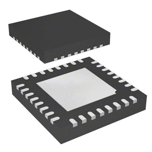
| 供应商器件封装 | 20-SOIC |
| 其它名称 | PIC18F13K22ISO |
| 包装 | 管件 |
| 可用A/D通道 | 12 |
| 可编程输入/输出端数量 | 17 |
| 商标 | Microchip Technology |
| 处理器系列 | PIC18 |
| 外设 | 欠压检测/复位,POR,PWM,WDT |
| 安装风格 | SMD/SMT |
| 定时器数量 | 4 Timer |
| 封装 | Tube |
| 封装/外壳 | 20-SOIC(0.295",7.50mm 宽) |
| 封装/箱体 | SOIC-20 |
| 工作温度 | -40°C ~ 85°C |
| 工作电源电压 | 3 V to 5.5 V |
| 工厂包装数量 | 38 |
| 振荡器类型 | 内部 |
| 接口类型 | I2C, MSSP, SPI, USART |
| 数据RAM大小 | 256 B |
| 数据总线宽度 | 8 bit |
| 数据转换器 | A/D 12x10b |
| 最大工作温度 | + 85 C |
| 最大时钟频率 | 64 MHz |
| 最小工作温度 | - 40 C |
| 标准包装 | 38 |
| 核心 | PIC |
| 核心处理器 | PIC |
| 核心尺寸 | 8-位 |
| 片上ADC | Yes |
| 电压-电源(Vcc/Vdd) | 2.3 V ~ 5.5 V |
| 电源电压-最大 | 5.5 V |
| 电源电压-最小 | 1.8 V, 2.7 V |
| 程序存储器大小 | 8 kB |
| 程序存储器类型 | 闪存 |
| 程序存储容量 | 8KB(4K x 16) |
| 系列 | PIC18 |
| 输入/输出端数量 | 17 I/O |
| 连接性 | I²C, LIN, SPI, UART/USART |
| 速度 | 64MHz |
| 配用 | /product-detail/zh/AC244033/AC244033-ND/2651277 |


- 商务部:美国ITC正式对集成电路等产品启动337调查
- 曝三星4nm工艺存在良率问题 高通将骁龙8 Gen1或转产台积电
- 太阳诱电将投资9.5亿元在常州建新厂生产MLCC 预计2023年完工
- 英特尔发布欧洲新工厂建设计划 深化IDM 2.0 战略
- 台积电先进制程称霸业界 有大客户加持明年业绩稳了
- 达到5530亿美元!SIA预计今年全球半导体销售额将创下新高
- 英特尔拟将自动驾驶子公司Mobileye上市 估值或超500亿美元
- 三星加码芯片和SET,合并消费电子和移动部门,撤换高东真等 CEO
- 三星电子宣布重大人事变动 还合并消费电子和移动部门
- 海关总署:前11个月进口集成电路产品价值2.52万亿元 增长14.8%


PDF Datasheet 数据手册内容提取
PIC18(L)F1XK22 20-Pin Flash Microcontrollers with XLP Technology High-Performance RISC CPU Analog Features • C Compiler Optimized Architecture: • Analog-to-Digital Converter (ADC) module - Optional extended instruction set designed to - 10-bit resolution, 12 channels optimize re-entrant code - Auto-acquisition capability • 256bytes Data EEPROM - Conversion available during Sleep • Up to 16 Kbytes Linear Program Memory • Analog Comparator module: Addressing - Two rail-to-rail analog comparators • Up to 512bytes Linear Data Memory Addressing - Independent input multiplexing • Up to 16 MIPS Operation - Inputs and outputs externally accessible • 16-bit Wide Instructions, 8-bit Wide Data Path • Voltage Reference module: • Priority Levels for Interrupts - Fixed Voltage Reference (FVR) with 1.024V, • 31-Level, Software Accessible Hardware Stack 2.048V and 4.096V output levels • 8 x 8 Single-Cycle Hardware Multiplier - 5-bit rail-to-rail resistive Digital-to-Analog Converter (DAC) with positive and negative Flexible Oscillator Structure reference selection • Precision 16MHz Internal Oscillator Block: Peripheral Highlights - Factory calibrated to ± 1% • 17 I/O Pins and 1 Input-only Pin: - Software selectable frequencies range of - High current sink/source 25mA/25mA 31kHz to 16MHz - Programmable weak pull-ups - 64MHz performance available using PLL – - Programmable interrupt-on- change no external components required - Three external interrupt pins • Four Crystal modes up to 64MHz • Four Timer modules: • Two External Clock modes up to 64MHz - Three 16-bit timers/counters with prescaler • 4X Phase Lock Loop (PLL) - One 8-bit timer/counter with 8-bit period • Secondary Oscillator using Timer1 @ 32kHz register, prescaler and postscaler • Fail-Safe Clock Monitor - Dedicated, low-power Timer1 oscillator - Allows for safe shutdown if peripheral clock • Enhanced Capture/Compare/PWM (ECCP) stops module: • Two-Speed Oscillator Start-up - One, two or four PWM outputs Special Microcontroller Features - Selectable polarity - Programmable dead time • 2.3V - 5.5V Operation – PIC18F1XK22 - Auto-shutdown and Auto-restart • 1.8V-3.6V Operation – PIC18LF1XK22 - PWM output steering control • Self-reprogrammable under Software Control • Master Synchronous Serial Port (MSSP) module • Power-on Reset (POR), Power-up Timer (PWRT) - 3-wire SPI (supports all four SPI modes) and Oscillator Start-up Timer (OST) - I2C Master and Slave modes (Slave mode • Programmable Brown-out Reset (BOR) address masking) • Extended Watchdog Timer (WDT): • Enhanced Universal Synchronous Asynchronous - Programmable period from 4 ms to 131s Receiver Transmitter module (EUSART) • Programmable Code Protection - Supports RS-232, RS-485 and LIN 2.0 • In-Circuit Serial Programming™ (ICSP™) via - Auto-Baud Detect two pins - Auto Wake-up on Break • In-Circuit Debug via Two Pins • SR Latch (555 Timer) module with: Extreme Low-Power Management - Configurable inputs and outputs PIC18LF1XK22 with XLP Technology - Supports mTouch® capacitive sensing applications • Sleep mode: 34 nA • Watchdog Timer: 460 nA • Timer1 Oscillator: 650 nA @ 32 kHz 2009-2016 Microchip Technology Inc. DS40001365F-page 1
PIC18(L)F1XK22 PIC18(L)F1XK22 Family Types Device a Sheet Index PBroygterasm MWemorodrsy (SbRyDtAaeMtsa) MeEm(EbDoPyarRtyetaOs )M Pins I/O(1) 10-bit A/DChannels omparators Timers8-bit/16-bit ECCP MSSP EUSART SR Latch at C D PIC18(L)F13K22 (1) 8K 4K 256 256 20 18 12-ch 2 1 / 3 1 1 1 Yes PIC18(L)F14K22 (1) 16K 8K 512 256 20 18 12-ch 2 1 / 3 1 1 1 Yes Note1: One pin is input-only. Data Sheet Index: (Unshaded devices are described in this document) 1. DS40001365 PIC18(L)F1XK22 20-Pin Flash Microcontrollers with XLP Technology Note: For other small form-factor package availability and marking information, please visit http://www.microchip.com/packaging or contact your local sales office. Pin Diagrams FIGURE 1: 20-PIN PDIP, SSOP, SOIC VDD 1 20 VSS RA5 2 19 RA0/PGD RA4 3 22 22 18 RA1/PGC RA3/MCLR/VPP 4 K K 17 RA2 3 4 RC5 5 F1 F1 16 RC0 RC4 6 L) L) 15 RC1 RC3/PGM 7 8( 8( 14 RC2 1 1 RC6 8 C C 13 RB4 RC7 9 PI PI 12 RB5 RB7 10 11 RB6 Note: See Table1 for location of all peripheral functions. FIGURE 2: 20-PIN QFN (4x4) D G P 45 DS0/ AA DSA RRVVR 2019181716 RA3/MCLR/VPP 1 15 RA1/PGC RC5 2 PIC18(L)F13K2214 RA2 RC4 3 13 RC0 PIC18(L)F14K22 RC3/PGM 4 12 RC1 RC6 5 11 RC2 6 7 8 910 77654 CBBBB RRRRR Note: See Table1 for location of all peripheral functions. DS40001365F-page 2 2009-2016 Microchip Technology Inc.
PIC18(L)F1XK22 TABLE 1: 20-PIN ALLOCATION TABLE (PIC18(L)F1XK22) C OI S I/O n PDIP/SSOP/ 20-Pin QFN Analog Comparator Reference ECCP EUSART MSSP SR Latch Timers Interrupts Pull-up Basic Pi 0- 2 RA0 19 16 AN0 C1IN+ VREF-/ — — — — — IOC/INT0 Y PGD CVREF(DAC1OUT) RA1 18 15 AN1 C12IN0- VREF+ — — — — — IOC/INT1 Y PGC RA2 17 14 AN2 C1OUT — — — — SRQ T0CKI IOC/INT2 Y — RA3 4 1 — — — — — — — — IOC Y MCLR/VPP RA4 3 20 AN3 — — — — — — — IOC Y OSC2/CLKOUT RA5 2 19 — — — — — — — T13CKI IOC Y OSC1/CLKIN RB4 13 10 AN10 — — — — SDI/SDA — — IOC Y — RB5 12 9 AN11 — — — RX/DT — — — IOC Y — RB6 11 8 — — — — — SCL/SCK — — IOC Y — RB7 10 7 — — — — TX/CK — — — IOC Y — RC0 16 13 AN4 C2IN+ — — — — — — — — — RC1 15 12 AN5 C12IN1- — — — — — — — — — RC2 14 11 AN6 C12IN2- — P1D — — — — — — — RC3 7 4 AN7 C12IN3- — P1C — — — — — — PGM RC4 6 3 — C2OUT — P1B — — SRNQ — — — — RC5 5 2 — — — CCP1/P1A — — — — — — — RC6 8 5 AN8 — — — — SS — — — — — RC7 9 6 AN9 — — — — SDO — — — — — — 1 18 — — — — — — — — — — VDD — 20 17 — — — — — — — — — — VSS 2009-2016 Microchip Technology Inc. DS40001365F-page 3
PIC18(L)F1XK22 Table of Contents 1.0 Device Overview..........................................................................................................................................................................6 2.0 Oscillator Module........................................................................................................................................................................12 3.0 Memory Organization.................................................................................................................................................................24 4.0 Flash Program Memory..............................................................................................................................................................45 5.0 Data EEPROM Memory.............................................................................................................................................................54 6.0 8 x 8 Hardware Multiplier............................................................................................................................................................58 7.0 Interrupts....................................................................................................................................................................................60 8.0 I/O Ports.....................................................................................................................................................................................73 9.0 Timer0 Module...........................................................................................................................................................................91 10.0 Timer1 Module...........................................................................................................................................................................94 11.0 Timer2 Module.........................................................................................................................................................................100 12.0 Timer3 Module.........................................................................................................................................................................102 13.0 Enhanced Capture/Compare/PWM (ECCP) Module................................................................................................................106 14.0 Master Synchronous Serial Port (MSSP) Module....................................................................................................................127 15.0 Enhanced Universal Synchronous Asynchronous Receiver Transmitter (EUSART)...............................................................170 16.0 Analog-to-Digital Converter (ADC) Module..............................................................................................................................197 17.0 Comparator Module..................................................................................................................................................................210 18.0 Power-Managed Modes...........................................................................................................................................................222 19.0 SR Latch...................................................................................................................................................................................228 20.0 Fixed Voltage Reference (FVR)................................................................................................................................................231 21.0 Digital-to-Analog Converter (DAC) Module..............................................................................................................................233 22.0 Reset........................................................................................................................................................................................237 23.0 Special Features of the CPU....................................................................................................................................................249 24.0 Instruction Set Summary..........................................................................................................................................................265 25.0 Development Support...............................................................................................................................................................315 26.0 Electrical Specifications............................................................................................................................................................319 27.0 DC and AC Characteristics Graphs and Charts.......................................................................................................................356 28.0 Packaging Information..............................................................................................................................................................372 Appendix A: Revision History.............................................................................................................................................................382 Appendix B: Device Differences.........................................................................................................................................................383 The Microchip WebSite......................................................................................................................................................................384 Customer Change Notification Service..............................................................................................................................................384 Customer Support..............................................................................................................................................................................384 Product Identification System.............................................................................................................................................................385 Worldwide Sales and Service............................................................................................................................................................387 DS40001365F-page 4 2009-2016 Microchip Technology Inc.
PIC18(L)F1XK22 TO OUR VALUED CUSTOMERS It is our intention to provide our valued customers with the best documentation possible to ensure successful use of your Microchip products. To this end, we will continue to improve our publications to better suit your needs. Our publications will be refined and enhanced as new volumes and updates are introduced. If you have any questions or comments regarding this publication, please contact the Marketing Communications Department via E-mail at docerrors@microchip.com. We welcome your feedback. Most Current Data Sheet To obtain the most up-to-date version of this data sheet, please register at our Worldwide Website at: http://www.microchip.com You can determine the version of a data sheet by examining its literature number found on the bottom outside corner of any page. The last character of the literature number is the version number, (e.g., DS30000000A is version A of document DS30000000). Errata An errata sheet, describing minor operational differences from the data sheet and recommended workarounds, may exist for current devices. As device/documentation issues become known to us, we will publish an errata sheet. The errata will specify the revision of silicon and revision of document to which it applies. To determine if an errata sheet exists for a particular device, please check with one of the following: • Microchip’s Worldwide Website; http://www.microchip.com • Your local Microchip sales office (see last page) When contacting a sales office, please specify which device, revision of silicon and data sheet (include literature number) you are using. Customer Notification System Register on our website at www.microchip.com to receive the most current information on all of our products. 2009-2016 Microchip Technology Inc. DS40001365F-page 5
PIC18(L)F1XK22 1.0 DEVICE OVERVIEW 1.1.2 MULTIPLE OSCILLATOR OPTIONS AND FEATURES This family offers the advantages of all PIC18 microcontrollers – namely, high computational All of the devices in the PIC18(L)F1XK22 family offer performance with the addition of high-endurance, ten different oscillator options, allowing users a wide Flash program memory. On top of these features, the range of choices in developing application hardware. PIC18(L)F1XK22 family introduces design These include: enhancements that make these microcontrollers a • Four Crystal modes, using crystals or ceramic logical choice for many high-performance, power resonators sensitive applications. • External Clock modes, offering the option of using two pins (oscillator input and a divide-by-4 clock 1.1 New Core Features output) or one pin (oscillator input, with the second pin reassigned as general I/O) 1.1.1 XLP TECHNOLOGY • External RC Oscillator modes with the same pin All of the devices in the PIC18(L)F1XK22 family options as the External Clock modes incorporate a range of features that can significantly • An internal oscillator block which contains a reduce power consumption during operation. Key 16MHz HFINTOSC oscillator and a 31kHz items include: LFINTOSC oscillator which together provide eight • Multiple Idle Modes: The controller can also run user selectable clock frequencies, from 31kHz to with its CPU core disabled but the peripherals still 16MHz. This option frees the two oscillator pins active. In these states, power consumption can be for use as additional general purpose I/O. reduced even further, to as little as 4% of normal • A Phase Lock Loop (PLL) frequency multiplier, operation requirements. available to both the high-speed crystal and • On-the-fly Mode Switching: The internal oscillator modes, which allows clock power-managed modes are invoked by user code speeds of up to 64MHz. Used with the internal during operation, allowing the user to incorporate oscillator, the PLL gives users a complete power-saving ideas into their application’s selection of clock speeds, from 31kHz to 64MHz software design. – all without using an external crystal or clock • Low Consumption in Key Modules: The circuit. power requirements for both Timer1 and the Besides its availability as a clock source, the internal Watchdog Timer are minimized. See oscillator block provides a stable reference source that Section26.0 “Electrical Specifications” gives the family additional features for robust for values. operation: • Fail-Safe Clock Monitor: This option constantly monitors the main clock source against a reference signal provided by the LFINTOSC. If a clock failure occurs, the controller is switched to the internal oscillator block, allowing for continued operation or a safe application shutdown. • Two-Speed Start-up: This option allows the internal oscillator to serve as the clock source from Power-on Reset, or wake-up from Sleep mode, until the primary clock source is available. DS40001365F-page 6 2009-2016 Microchip Technology Inc.
PIC18(L)F1XK22 1.2 Other Special Features 1.3 Details on Individual Family Members • Memory Endurance: The Flash cells for both program memory and data EEPROM are rated to Devices in the PIC18(L)F1XK22 family are available in last for many thousands of erase/write cycles – up to 20-pin packages. Block diagrams for the two groups 10K for program memory and 100K for EEPROM. are shown in Figure1-1. Data retention without refresh is conservatively The devices are differentiated from each other in the estimated to be greater than 40 years. following ways: • Self-programmability: These devices can write to their own program memory spaces under 1. Flash program memory: internal software control. Using a bootloader • 8Kbytes for PIC18(L)F13K22 routine located in the code protected Boot Block, • 16Kbytes for PIC18(L)F14K22 it is possible to create an application that can All other features for devices in this family are identical. update itself in the field. These are summarized in Table1-1. • Extended Instruction Set: The PIC18(L)F1XK22 The pinouts for all devices are listed in Table1 and I/O family introduces an optional extension to the description are in Table1-2. PIC18 instruction set, which adds eight new instructions and an Indexed Addressing mode. This extension has been specifically designed to optimize re-entrant application code originally developed in high-level languages, such as C. • Enhanced CCP module: In PWM mode, this module provides one, two or four modulated outputs for controlling half-bridge and full-bridge drivers. Other features include: - Auto-Shutdown, for disabling PWM outputs on interrupt or other select conditions - Auto-Restart, to reactivate outputs once the condition has cleared - Output steering to selectively enable one or more of four outputs to provide the PWM signal. • Enhanced Addressable USART: This serial communication module is capable of standard RS-232 operation and provides support for the LIN bus protocol. Other enhancements include automatic baud rate detection and a 16-bit Baud Rate Generator for improved resolution. • 10-bit A/D Converter: This module incorporates programmable acquisition time, allowing for a channel to be selected and a conversion to be initiated without waiting for a sampling period and thus, reduce code overhead. • Extended Watchdog Timer (WDT): This enhanced version incorporates a 16-bit postscaler, allowing an extended time-out range that is stable across operating voltage and temperature. See Section26.0 “Electrical Specifications” for time-out periods. 2009-2016 Microchip Technology Inc. DS40001365F-page 7
PIC18(L)F1XK22 TABLE 1-1: DEVICE FEATURES FOR THE PIC18(L)F1XK22 (20-PIN DEVICES) Features PIC18F13K22 PIC18LF13K22 PIC18F14K22 PIC18LF14K22 Voltage Range (1.8 - 5.5V) 2.3-5.5V 1.8V-3.6V 2.3-5.5V 1.8V-3.6V Program Memory (Bytes) 8K 16K Program Memory (Instructions) 4096 8192 Data Memory (Bytes) 256 512 Operating Frequency DC – 64 MHz Interrupt Sources 30 I/O Ports Ports A, B, C Timers 4 Enhanced Capture/ Compare/PWM Modules 1 Serial Communications MSSP, Enhanced USART 10-Bit Analog-to-Digital Module 12 Input Channels Resets (and Delays) POR, BOR, RESET Instruction, Stack Full, Stack Underflow, MCLR, WDT (PWRT, OST) Instruction Set 75 Instructions, 83 with Extended Instruction Set Enabled Packages 20-Pin PDIP, SSOP, SOIC QFN (4x4x0.9mm) DS40001365F-page 8 2009-2016 Microchip Technology Inc.
PIC18(L)F1XK22 FIGURE 1-1: PIC18(L)F1XK22 BLOCK DIAGRAM Data Bus<8> Table Pointer<21> 8 8 Data Latch PORTA inc/dec logic RA0 Data Memory RA1 21 PCLAT U PCLATH (512/768 bytes) RA1 RA3 20 Address Latch RA4 PCU PCH PCL RA5 Program Counter 12 Data Address<12> 31-Level Stack Address Latch 4 12 4 BSR Access Program Memory STKPTR FSR0 Bank FSR1 Data Latch FSR2 12 PORTB RB4 inc/dec 8 logic RB5 Table Latch RB6 RB7 Address ROM Latch Instruction Bus <16> Decode IR 8 Instruction State machine Decode and control signals Control PRODH PRODL PORTC 8 x 8 Multiply RC0 3 8 RC1 RC2 BITOP W RC3 Internal Power-up 8 8 8 RC4 OSC1(2) Oscillator Timer RC5 Block RC6 Oscillator 8 8 RC7 LFINTOSC Start-up Timer OSC2(2) Oscillator ALU<8> Power-on 16 MHz Reset 8 Oscillator MCLR(1) Watchdog Timer Single-Supply VDD,VSS Programming Fail-Safe BParencdi sGioanp FVR Clock Monitor Reference DAC Data BOR EEPROM Timer0 Timer1 Timer2 Timer3 FVR FVR ADC CVREF/DAC1 Comparator ECCP1 MSSP EUSART 10-bit CVREF/DAC1 Note 1: RA3 is only available when MCLR functionality is disabled. 2: OSC1/CLKIN and OSC2/CLKOUT are only available in select oscillator modes and when these pins are not being used as digital I/O. Refer to Section2.0 “Oscillator Module” for additional information. 2009-2016 Microchip Technology Inc. DS40001365F-page 9
PIC18(L)F1XK22 TABLE 1-2: PIC18(L)F1XK22 PIN SUMMARY Pin Number P/ O Pin Buffer Pin Name P/SSSOIC QFN Type Type Description DI P RA0/AN0/CVREF/VREF-/C1IN+/INT0/PGD 19 16 RA0 I/O TTL Digital I/O AN0 I Analog ADC channel 0 CVREF/DAC1OUT O Analog DAC reference voltage output VREF- I Analog ADC and DAC reference voltage (low) input C1IN+ I Analog Comparator C1 noninverting input INT0 I ST External interrupt 0 PGD I/O ST ICSP™ programming data pin RA1/AN1/C12IN0-/VREF+/INT1/PGC 18 15 RA1 I/O TTL Digital I/O AN1 I Analog ADC channel 1 C12IN0- 1 Analog Comparator C1 and C2 inverting input VREF+ I Analog ADC and DAC reference voltage (high) input INT1 I ST External interrupt 1 PGC I/O ST ICSP programming clock pin RA2/AN2/C1OUT/T0CKI/INT2/SRQ 17 14 RA2 I/O ST Digital I/O AN2 I Analog ADC channel 2 C1OUT — CMOS Comparator C1 output T0CKI I ST Timer0 external clock input INT2 I ST External interrupt 2 SRQ O CMOS SR latch output RA3/MCLR/VPP 4 1 RA3 I ST Digital input MCLR I ST Active-low Master Clear with internal pull-up VPP P — High voltage programming input RA4/AN3/OSC2/CLKOUT 3 20 RA4 I/O TTL Digital I/O AN3 I Analog ADC channel 3 OSC2 O XTAL Oscillator crystal output. Connect to crystal or resonator in Crystal Oscillator mode CLKOUT O CMOS In RC mode, OSC2 pin outputs CLKOUT which has 1/4 the frequency of OSC1 and denotes the instruction cycle rate RA5/OSC1/CLKIN/T13CKI 2 19 RA5 I/O TTL Digital I/O OSC1 I XTAL Oscillator crystal input or external clock input ST buffer when configured in RC mode; analog other wise CLKIN I CMOS External clock source input. Always associated with the pin function OSC1 (See related OSC1/CLKIN, OSC2, CLKOUT pins T13CKI I ST Timer0 and Timer3 external clock input RB4/AN10/SDI/SDA 13 10 RB4 I/O TTL Digital I/O AN10 I Analog ADC channel 10 SDI I ST SPI data in SDA I/O ST I2C data I/O Legend: TTL = TTL compatible input CMOS = CMOS compatible input or output ST = Schmitt Trigger input I = Input O = Output P = Power XTAL= Crystal Oscillator DS40001365F-page 10 2009-2016 Microchip Technology Inc.
PIC18(L)F1XK22 TABLE 1-2: PIC18(L)F1XK22 PIN SUMMARY (CONTINUED) Pin Number P/ Pin Name P/SSOSOIC QFN TPyipne BTuyfpfeer Description DI P RB5/AN11/RX/DT 12 9 RB5 I/O TLL Digital I/O AN11 I Analog ADC channel 11 RX I ST EUSART asynchronous receive DT I/O ST EUSART synchronous data (see related RX/TX) RB6/SCK/SCL 11 8 RB6 I/O TLL Digital I/O SCK I/O ST Synchronous serial clock input/output for SPI mode SCL I/O ST Synchronous serial clock input/output for I2C mode RB7/TX/CK 10 7 RB7 I/O TLL Digital I/O TX O CMOS EUSART asynchronous transmit CK I/O ST EUSART synchronous clock (see related RX/DT) RC0/AN4/C2IN+ 16 13 RC0 I/O ST Digital I/O AN4 I Analog ADC channel 4 C2IN+ I Analog Comparator C2 noninverting input RC1/AN5/C12IN- 15 12 RC1 I/O ST Digital I/O AN5 I Analog ADC channel 5 C12IN- I Analog Comparator C1 and C2 inverting input RC2/AN6/C12IN2-/P1D 14 11 RC2 I/O ST Digital I/O AN6 I Analog ADC channel 6 C12IN2- I Analog Comparator C1 and C2 inverting input P1D O CMOS Enhanced CCP1 PWM output RC3/AN7/C12IN3-/P1C/PGM 7 4 RC3 I/O ST Digital I/O AN7 I Analog ADC channel 7 C12IN3- I Analog Comparator C1 and C2 inverting input P1C O CMOS Enhanced CCP1 PWM output PGM I/O ST Low-Voltage ICSP Programming enable pin RC4/C2OUT/P1B/SRNQ 6 3 RC4 I/O ST Digital I/O C2OUT O CMOS Comparator C2 output P1B O CMOS Enhanced CCP1 PWM output SRNQ O CMOS SR latch inverted output RC5/CCP1/P1A 5 2 RC5 I/O ST Digital I/O CCP1 I/O ST Capture 1 input/Compare 1 output/PWM 1 output P1A O CMOS Enhanced CCP1 PWM output RC6/AN8/SS 8 5 RC6 I/O ST Digital I/O AN8 I Analog ADC channel 8 SS I TTL SPI slave select input RC7/AN9/SDO 9 6 RC7 I/O ST Digital I/O AN9 I Analog ADC channel 9 SDO O CMOS SPI data out VSS 20 17 P — Ground reference for logic and I/O pins VDD 1 18 P — Positive supply for logic and I/O pins Legend: TTL = TTL compatible input CMOS = CMOS compatible input or output ST = Schmitt Trigger input I = Input O = Output P = Power XTAL= Crystal Oscillator 2009-2016 Microchip Technology Inc. DS40001365F-page 11
PIC18(L)F1XK22 2.0 OSCILLATOR MODULE 2.3 System Clock Selection The SCS bits of the OSCCON register select between 2.1 Overview the following clock sources: The oscillator module has a variety of clock sources • Primary External Oscillator and features that allow it to be used in a wide range of • Secondary External Oscillator applications, maximizing performance and minimizing • Internal Oscillator power consumption. Figure2-1 illustrates a block diagram of the oscillator module. Note: The frequency of the system clock will be referred to as FOSC throughout this Key features of the oscillator module include: document. • System Clocks • System Clock Selection TABLE 2-1: SYSTEM CLOCK SELECTION - Primary External Oscillator Configuration Selection - Secondary External Oscillator SCS <1:0> System Clock - Internal Oscillator 1x Internal Oscillator • Oscillator Start-up Timer • System Clock Selection 01 Secondary External Oscillator • Clock Switching 00 Oscillator defined by (Default after Reset) FOSC<3:0> • 4x Phase Lock Loop Frequency Multiplier • CPU Clock Divider The default state of the SCS bits sets the system clock • Two-Speed Start-up Mode to be the oscillator defined by the FOSC bits of the CONFIG1H Configuration register. The system clock • Fail-Safe Clock Monitoring will always be defined by the FOSC bits until the SCS bits are modified in software. 2.2 System Clocks When the Internal Oscillator is selected as the system The PIC18(L)F1XK22 can be operated in 13 different clock, the IRCF bits of the OSCCON register and the oscillator modes. The user can program these using INTSRC bit of the OSCTUNE register will select either the available Configuration bits. In addition, clock the LFINTOSC or the HFINTOSC. The LFINTOSC is support functions such as Fail-Safe and two Start-up selected when the IRCF<2:0>=000 and the INTSRC can also be configured. bit is clear. All other combinations of the IRCF bits and The available Primary oscillator options include: the INTSRC bit will select the HFINTOSC as the system clock. • External Clock, low power (ECL) • External Clock, medium power (ECM) 2.4 Primary External Oscillator • External Clock, high power (ECH) The Primary External Oscillator’s mode of operation is • External Clock, low power, CLKOUT function on selected by setting the FOSC<3:0> bits of the RA4/OSC2 (ECCLKOUTL) CONFIG1H Configuration register. The oscillator can • External Clock, medium power, CLKOUT function be set to the following modes: on RA4/OSC2 (ECCLKOUTM) • LP: Low-Power Crystal • External Clock, high power, CLKOUT function on RA4/OSC2 (ECCLKOUTH) • XT: Crystal/Ceramic Resonator • External Crystal (XT) • HS: High-Speed Crystal Resonator • High-speed Crystal (HS) • RC: External RC Oscillator • Low-power crystal (LP) • EC: External Clock • External Resistor/Capacitor (EXTRC) Additionally, the Primary External Oscillator may be • External RC, CLKOUT function on RA4/OSC2 shut down under firmware control to save power. • 31.25kHz – 16MHz internal oscillator (INTOSC) • 31.25kHz – 16MHz internal oscillator, CLKOUT function on RA4/OSC2 Additionally, the 4x PLL may be enabled in hardware or software (under certain conditions) for increased oscillator speed. DS40001365F-page 12 2009-2016 Microchip Technology Inc.
PIC18(L)F1XK22 FIGURE 2-1: PIC® MCU CLOCK SOURCE BLOCK DIAGRAM Primary PIC18(L)F1XK22 Oscillator, External and Timer1/Timer3 OSC1/T13CKI Secondary Oscillator Sleep PCLKEN LP, XT, HS, RC, EC, IDLEN PRI_SD 4 x PLL 1 Secondary Osc. OSC2 0x Sleep 0 T1OSCEN FOSC<3:0> Peripherals PLL_EN PLLEN Internal Osc. 1xUX SCylosctekm M CPU IRCF<2:0> Sleep 16 MHz 8 MHz Internal 110 Oscillator 4 MHz Block er 2 MHz 101 HF1I6N MTOHSzC stscal 1 MHz 100101MUX CColonctrkol FSOCSS<C1<:30:>0 > Po 500 kHz 31 kHz 010 LFINTOSC 250 kHz 001 1 31 kHz 000 0 INTSRC Fail-Safe Clock Watchdog Timer Two-Speed Start-up Note: If using a low-frequency external oscillator and want to multiple it by 4 via PLL, the ideal input frequency is from 4MHz to 16MHz. 2009-2016 Microchip Technology Inc. DS40001365F-page 13
PIC18(L)F1XK22 2.4.1 PRIMARY EXTERNAL OSCILLATOR FIGURE 2-2: QUARTZ CRYSTAL SHUTDOWN OPERATION (LP, XT OR HS MODE) The Primary External Oscillator can be enabled or disabled via software. To enable software control of the Primary External Oscillator, the PCLKEN bit of the PIC® MCU CONFIG1H Configuration register must be set. With the PCLKEN bit set, the Primary External Oscillator is OSC1/CLKIN controlled by the PRI_SD bit of the OSCCON2 register. C1 To Internal The Primary External Oscillator will be enabled when Logic the PRI_SD bit is set, and disabled when the PRI_SD bit is clear. QCruyasrttazl RF(2) Sleep Note: The Primary External Oscillator cannot be shut down when it is selected as the C2 RS(1) OSC2/CLKOUT System Clock. To shut down the oscillator, the system clock source must be either the Secondary Oscillator or the Internal Note 1: A series resistor (RS) may be required for quartz crystals with low drive level. Oscillator. 2: The value of RF varies with the Oscillator mode selected (typically between 2M to 10M. 2.4.2 LP, XT AND HS OSCILLATOR MODES Note 1: Quartz crystal characteristics vary The LP, XT and HS modes support the use of quartz according to type, package and crystal resonators or ceramic resonators connected to manufacturer. The user should consult the OSC1 and OSC2 (Figure2-2). The mode selects a low, manufacturer data sheets for specifications medium or high gain setting of the internal inverter- and recommended application. amplifier to support various resonator types and speed. 2: Always verify oscillator performance over LP Oscillator mode selects the lowest gain setting of the the VDD and temperature range that is internal inverter-amplifier. LP mode current consumption expected for the application. is the least of the three modes. This mode is best suited to drive resonators with a low drive level specification, for 3: For oscillator design assistance, reference example, tuning fork type crystals. the following Microchip Applications Notes: XT Oscillator mode selects the intermediate gain • AN826, Crystal Oscillator Basics and setting of the internal inverter-amplifier. XT mode Crystal Selection for rfPIC® and current consumption is the medium of the three modes. PICmicro® Devices (DS00826) This mode is best suited to drive resonators with a • AN849, Basic PICmicro® Oscillator medium drive level specification. Design (DS00849) HS Oscillator mode selects the highest gain setting of the • AN943, Practical PICmicro® Oscillator internal inverter-amplifier. HS mode current consumption Analysis and Design (DS00943) is the highest of the three modes. This mode is best • AN949, Making Your Oscillator Work suited for resonators that require a high drive setting. (DS00949) Figure2-2 and Figure2-3 show typical circuits for quartz crystal and ceramic resonators, respectively. DS40001365F-page 14 2009-2016 Microchip Technology Inc.
PIC18(L)F1XK22 FIGURE 2-3: CERAMIC RESONATOR The RC oscillator frequency is a function of the supply OPERATION voltage, the resistor REXT, the capacitor CEXT and the (XT OR HS MODE) operating temperature. Other factors affecting the oscillator frequency are: PIC® MCU • Input threshold voltage variation • Component tolerances OSC1/CLKIN • Variation in capacitance due to packaging C1 To Internal 2.4.4 EXTERNAL CLOCK Logic The External Clock (EC) mode allows an externally RP(3) RF(2) Sleep generated logic level clock to be used as the system’s clock source. When operating in this mode, the external clock source is connected to the OSC1 C2 Ceramic RS(1) OSC2/CLKOUT allowing OSC2 to be configured as an I/O or as Resonator CLKOUT. The CLKOUT function is selected by the FOSC bits of the CONFIG1H Configuration register. Note 1: A series resistor (RS) may be required for When OSC2 is configured as CLKOUT, the frequency ceramic resonators with low drive level. at the pin is the frequency of the EC oscillator divided 2: The value of RF varies with the Oscillator mode by 4. selected (typically between 2M to 10M. Three different power settings are available for EC 3: An additional parallel feedback resistor (RP) may be required for proper ceramic resonator mode. The power settings allow for a reduced IDD of the operation. device, if the EC clock is known to be in a specific range. If there is an expected range of frequencies for the EC clock, select the power mode for the highest 2.4.3 EXTERNAL RC frequency. The External Resistor-Capacitor (RC) mode supports EC Low power 0 – 250kHz the use of an external RC circuit. This allows the EC Medium power 250kHz – 4MHz designer maximum flexibility in frequency choice while keeping costs to a minimum when clock accuracy is not EC High power 4 – 64MHz required. In RC mode, the RC circuit connects to OSC1, allowing OSC2 to be configured as an I/O or as 2.5 Secondary External Oscillator CLKOUT. The CLKOUT function is selected by the The Secondary External Oscillator is designed to drive FOSC bits of the CONFIG1H Configuration register. an external 32.768 kHz crystal. This oscillator is When OSC2 is configured as CLKOUT, the frequency enabled or disabled by the T1OSCEN bit of the T1CON at the pin is the frequency of the RC oscillator divided by register. See Section10.0 “Timer1 Module” for more 4. Figure2-4 shows the external RC mode connections. information. FIGURE 2-4: EXTERNAL RC MODES VDD PIC® MCU REXT OSC1/CLKIN Internal Clock CEXT VSS FOSC/4 or OSC2/CLKOUT(1) I/O(2) Recommended values: 10 k REXT 100 k CEXT > 20 pF Note 1: Alternate pin functions are listed in Section1.0 “Device Overview”. 2: Output depends upon RC or RCIO clock mode. 2009-2016 Microchip Technology Inc. DS40001365F-page 15
PIC18(L)F1XK22 2.6 Internal Oscillator 2.6.2 HFINTOSC The internal oscillator module contains two independent The High-Frequency Internal Oscillator (HFINTOSC) is oscillators which are: a precision oscillator that is factory-calibrated to operate at 16MHz. The output of the HFINTOSC • LFINTOSC: Low-Frequency Internal Oscillator connects to a postscaler and a multiplexer (see • HFINTOSC: High-Frequency Internal Oscillator Figure2-1). One of eight frequencies can be selected When operating with either oscillator, OSC1 will be an using the IRCF<2:0> bits of the OSCCON register. The I/O and OSC2 will be either an I/O or CLKOUT. The following frequencies are available from the CLKOUT function is selected by the FOSC bits of the HFINTOSC: CONFIG1H Configuration register. When OSC2 is • 16 MHZ configured as CLKOUT, the frequency at the pin is the • 8 MHZ frequency of the Internal Oscillator divided by 4. • 4 MHZ 2.6.1 LFINTOSC • 2 MHZ • 1 MHZ (Default after Reset) The Low-Frequency Internal Oscillator (LFINTOSC) is a 31kHz internal clock source. The LFINTOSC • 500 kHz oscillator is the clock source for: • 250 kHz • Power-up Timer • 31 kHz • Watchdog Timer The HFIOFS bit of the OSCCON register indicates • Fail-Safe Clock Monitor whether the HFINTOSC is stable. The LFINTOSC is enabled when any of the following Note1: Selecting 31kHz from the HFINTOSC conditions are true: oscillator requires IRCF<2:0>=000 and the INTSRC bit of the OSCTUNE register • Power-up Timer is enabled (PWRTEN=0) to be set. If the INTSRC bit is clear, the • Watchdog Timer is enabled (WDTEN=1) system clock will come from the • Watchdog Timer is enabled by software LFINTOSC. (WDTEN=0 and SWDTEN=1) 2: Additional adjustments to the frequency • Fail-Safe Clock Monitor is enabled (FCMEM= 1) of the HFINTOSC can made via the • SCS1=1 and IRCF<2:0>=000 and INTSRC=0 OSCTUNE registers. See Register2-3 • FOSC<3:0> selects the internal oscillator as the for more details. primary clock and IRCF<2:0>=000 and The HFINTOSC is enabled if any of the following INTSRC=0 conditions are true: • IESO=1 (Two-Speed Start-up) and IRCF<2:0>=000 and INTSRC=0 • SCS1=1 and IRCF<2:0>000 • SCS1=1 and IRCF<2:0>=000 and INTSRC=1 • FOSC<3:0> selects the internal oscillator as the primary clock and - IRCF<2:0>000 or - IRCF<2:0>=000 and INTSRC=1 • IESO=1 (Two-Speed Start-up) and - IRCF<2:0>000 or - IRCF<2:0>=000 and INTSRC=1 • FCMEM=1 (Fail-Safe Clock Monitoring) and - IRCF<2:0>000 or - IRCF<2:0>=000 and INTSRC=1 DS40001365F-page 16 2009-2016 Microchip Technology Inc.
PIC18(L)F1XK22 2.7 Oscillator Control The Oscillator Control (OSCCON) (Register2-1) and the Oscillator Control 2 (OSCCON2) (Register2-2) registers control the system clock and frequency selection options. REGISTER 2-1: OSCCON: OSCILLATOR CONTROL REGISTER R/W-0 R/W-0 R/W-1 R/W-1 R-q R-0 R/W-0 R/W-0 IDLEN IRCF2 IRCF1 IRCF0 OSTS(1) HFIOFS SCS1 SCS0 bit 7 bit 0 Legend: R = Readable bit W = Writable bit U = Unimplemented bit, read as ‘0’ q = depends on condition -n = Value at POR ‘1’ = Bit is set ‘0’ = Bit is cleared x = Bit is unknown bit 7 IDLEN: Idle Enable bit 1 = Device enters Idle mode on SLEEP instruction 0 = Device enters Sleep mode on SLEEP instruction bit 6-4 IRCF<2:0>: Internal Oscillator Frequency Select bits 111 = 16MHz 110 = 8MHz 101 = 4MHz 100 = 2MHz 011 = 1MHz(3) 010 = 500kHz 001 = 250kHz 000 = 31kHz(2) bit 3 OSTS: Oscillator Start-up Time-out Status bit(1) 1 = Device is running from the clock defined by FOSC<2:0> of the CONFIG1 register 0 = Device is running from the internal oscillator (HFINTOSC or LFINTOSC) bit 2 HFIOFS: HFINTOSC Frequency Stable bit 1 = HFINTOSC frequency is stable 0 = HFINTOSC frequency is not stable bit 1-0 SCS<1:0>: System Clock Select bits 1x = Internal oscillator block 01 = Secondary (Timer1) oscillator 00 = Primary clock (determined by CONFIG1H[FOSC<3:0>]). Note 1: Reset state depends on state of the IESO Configuration bit. 2: Source selected by the INTSRC bit of the OSCTUNE register, see text. 3: Default output frequency of HFINTOSC on Reset. 2009-2016 Microchip Technology Inc. DS40001365F-page 17
PIC18(L)F1XK22 REGISTER 2-2: OSCCON2: OSCILLATOR CONTROL REGISTER 2 U-0 U-0 U-0 U-0 U-0 R/W-1 R/W-0 R-x — — — — — PRI_SD HFIOFL LFIOFS bit 7 bit 0 Legend: R = Readable bit W = Writable bit U = Unimplemented bit, read as ‘0’ q = depends on condition -n = Value at POR ‘1’ = Bit is set ‘0’ = Bit is cleared x = Bit is unknown bit 7-3 Unimplemented: Read as ‘0’ bit 2 PRI_SD: Primary Oscillator Drive Circuit shutdown bit 1 = Oscillator drive circuit on 0 = Oscillator drive circuit off (zero power) bit 1 HFIOFL: HFINTOSC Frequency Locked bit 1 = HFINTOSC is in lock 0 = HFINTOSC has not yet locked bit 0 LFIOFS: LFINTOSC Frequency Stable bit 1 = LFINTOSC is stable 0 = LFINTOSC is not stable DS40001365F-page 18 2009-2016 Microchip Technology Inc.
PIC18(L)F1XK22 2.7.1 OSCTUNE REGISTER (PWRT), Watchdog Timer (WDT), Fail-Safe Clock Monitor (FSCM) and peripherals, are not affected by the The HFINTOSC is factory-calibrated, but can be change in frequency. adjusted in software by writing to the TUN<5:0> bits of the OSCTUNE register (Register2-3). The OSCTUNE register also implements the INTSRC and PLLEN bits, which control certain features of the The default value of the TUN<5:0> is ‘000000’. The internal oscillator block. value is a 6-bit two’s complement number. The INTSRC bit allows users to select which internal When the OSCTUNE register is modified, the oscillator provides the clock source when the 31kHz HFINTOSC frequency will begin shifting to the new frequency option is selected. This is covered in greater frequency. Code execution continues during this shift, detail in Section2.6.1 “LFINTOSC”. while giving no indication that the shift has occurred. The PLLEN bit controls the operation of the frequency OSCTUNE does not affect the LFINTOSC frequency. multiplier. For more details about the function of the The operation of features that depend on the LFINTOSC PLLEN bit see Section2.10 “4x Phase Lock Loop clock source frequency, such as the Power-up Timer Frequency Multiplier”. REGISTER 2-3: OSCTUNE: OSCILLATOR TUNING REGISTER R/W-0 R/W-0 R/W-0 R/W-0 R/W-0 R/W-0 R/W-0 R/W-0 INTSRC PLLEN TUN5 TUN4 TUN3 TUN2 TUN1 TUN0 bit 7 bit 0 Legend: R = Readable bit W = Writable bit U = Unimplemented bit, read as ‘0’ -n = Value at POR ‘1’ = Bit is set ‘0’ = Bit is cleared x = Bit is unknown bit 7 INTSRC: Internal Oscillator Low-Frequency Source Select bit 1 = 31.25kHz device clock derived from 16MHz HFINTOSC source (divide-by-512 enabled) 0 = 31kHz device clock derived directly from LFINTOSC internal oscillator bit 6 PLLEN: Frequency Multiplier PLL bit 1 = PLL enabled (for HFINTOSC 8MHz and 16 MHz only) 0 = PLL disabled bit 5-0 TUN<5:0>: Frequency Tuning bits 011111 = Maximum frequency 011110 = • • • 000001 = 000000 = Oscillator module is running at the factory-calibrated frequency. 111111 = • • • 100000 = Minimum frequency 2009-2016 Microchip Technology Inc. DS40001365F-page 19
PIC18(L)F1XK22 2.8 Oscillator Start-up Timer 2.9 Clock Switching The Primary External Oscillator, when configured for The device contains circuitry to prevent clock “glitches” LP, XT or HS modes, incorporates an Oscillator Start-up due to a change of the system clock source. To Timer (OST). The OST ensures that the oscillator starts accomplish this, a short pause in the system clock and provides a stable clock to the oscillator module. occurs during the clock switch. If the new clock source The OST times out when 1024 oscillations on OSC1 is not stable (e.g., OST is active), the device will have occurred. During the OST period, with the system continue to execute from the old clock source until the clock set to the Primary External Oscillator, the program new clock source becomes stable. The timing of a counter does not increment suspending program clock switch is as follows: execution. The OST period will occur following: 1. SCS<1:0> bits of the OSCCON register are • Power-on Reset (POR) modified. • Brown-out Reset (BOR) 2. The system clock will continue to operate from • Wake-up from Sleep the old clock until the new clock is ready. • Oscillator being enabled 3. Clock switch circuitry waits for two consecutive rising edges of the old clock after the new clock • Expiration of Power-up Timer (PWRT) is ready. In order to minimize latency between external oscillator 4. The system clock is held low, starting at the next start-up and code execution, the Two-Speed Start-up falling edge of the old clock. mode can be selected. See Section2.11 “Two-Speed 5. Clock switch circuitry waits for an additional two Start-up Mode” for more information. rising edges of the new clock. 6. On the next falling edge of the new clock, the low hold on the system clock is release and the new clock is switched in as the system clock. 7. Clock switch is complete. Refer to Figure2-5 for more details. FIGURE 2-5: CLOCK SWITCH TIMING High Speed Low Speed Old Clock Start-up Time(1) Clock Sync Running New Clock New Clk Ready IRCF <2:0> Select Old Select New System Clock Low Speed High Speed Old Clock Start-up Time(1) Clock Sync Running New Clock New Clk Ready IRCF <2:0>Select Old Select New System Clock Note 1: Start-up time includes TOST (1024 TOSC) for external clocks, plus TPLL (approx. 2 ms) for HSPLL mode. DS40001365F-page 20 2009-2016 Microchip Technology Inc.
PIC18(L)F1XK22 TABLE 2-2: EXAMPLES OF DELAYS DUE TO CLOCK SWITCHING Switch From Switch To Oscillator Delay Sleep/POR LFINTOSC Oscillator Warm-up Delay (TWARM) HFINTOSC Sleep/POR LP, XT, HS 1024 clock cycles Sleep/POR EC, RC 8 Clock Cycles 2.10 4x Phase Lock Loop Frequency 2.11 Two-Speed Start-up Mode Multiplier Two-Speed Start-up mode provides additional power A Phase Locked Loop (PLL) circuit is provided as an savings by minimizing the latency between external option for users who wish to use a lower-frequency Oscillator Start-up Timer (OST) and code execution. In external oscillator or to operate at 32MHz or 64MHz applications that make heavy use of the Sleep mode, with the HFINTOSC. The PLL is designed for an input Two-Speed Start-up will remove the OST period, which frequency from 4MHz to 16MHz. The PLL multiplies can reduce the overall power consumption of the its input frequency by a factor of four when the PLL is device. enabled. This may be useful for customers who are Two-Speed Start-up mode is enabled by setting the concerned with EMI, due to high-frequency crystals. IESO bit of the CONFIG1H Configuration register. With Two bits control the PLL: the PLL_EN bit of the Two-Speed Start-up enabled, the device will execute CONFIG1H Configuration register and the PLLEN bit of instructions using the internal oscillator during the the OSCTUNE register. The PLL is enabled when the Primary External Oscillator OST period. PLL_EN bit is set and it is under software control when When the system clock is set to the Primary External the PLL_EN bit is cleared. Refer to Table2-3 and Oscillator and the oscillator is configured for LP, XT or Table2-4 for more information. HS modes, the device will not execute code during the OST period. The OST will suspend program execution TABLE 2-3: PLL CONFIGURATION until 1024 oscillations are counted. Two-Speed Start-up mode minimizes the delay in code execution by PLL_EN PLLEN PLL Status operating from the internal oscillator while the OST is 1 x PLL enabled active. The system clock will switch back to the Primary 0 1 PLL enabled External Oscillator after the OST period has expired. 0 0 PLL disabled Two-speed Start-up will become active after: • Power-on Reset (POR) • Power-up Timer (PWRT), if enabled TABLE 2-4: PLL CONFIG1H/SOFTWARE • Wake-up from Sleep ENABLE CLOCK SOURCE RESTRICTIONS The OSTS bit of the OSCCON register reports which oscillator the device is currently using for operation. PLL CONFIG1H PLL Software The device is running from the oscillator defined by the Mode Enable (PLL_EN) Enable (PLLEN) FOSC bits of the CONFIG1H Configuration register LP Yes No when the OSTS bit is set. The device is running from the internal oscillator when the OSTS bit is clear. XT Yes No HS Yes No EC Yes No EXTRC Yes No LF INTOSC No No HF INTOSC 8/16 MHz 8/16 MHz 2009-2016 Microchip Technology Inc. DS40001365F-page 21
PIC18(L)F1XK22 2.12 Fail-Safe Clock Monitor 2.12.3 FAIL-SAFE CONDITION CLEARING The Fail-Safe Clock Monitor (FSCM) allows the device The Fail-Safe condition is cleared by either one of the to continue operating should the external oscillator fail. following: The FSCM can detect oscillator failure any time after • Any Reset the Oscillator Start-up Timer (OST) has expired. The • By toggling the SCS1 bit of the OSCCON register FSCM is enabled by setting the FCMEN bit in the Both of these conditions restart the OST. While the CONFIG1H Configuration register. The FSCM is OST is running, the device continues to operate from applicable to all external oscillator modes (LP, XT, HS, the INTOSC selected in OSCCON. When the OST EC and RC). times out, the Fail-Safe condition is cleared and the device automatically switches over to the external clock FIGURE 2-6: FSCM BLOCK DIAGRAM source. The Fail-Safe condition need not be cleared before the OSCFIF flag is cleared. Clock Monitor Latch External 2.12.4 RESET OR WAKE-UP FROM SLEEP S Q Clock The FSCM is designed to detect an oscillator failure after the Oscillator Start-up Timer (OST) has expired. The OST is used after waking up from Sleep and after LFINTOSC Oscillator ÷ 64 R Q any type of Reset. The OST is not used with the EC or RC Clock modes so that the FSCM will be active as 31 kHz 488 Hz soon as the Reset or wake-up has completed. When (~32 s) (~2 ms) the FSCM is enabled, the Two-Speed Start-up is also enabled. Therefore, the device will always be executing Sample Clock Clock code while the OST is operating. Failure Detected Note: Due to the wide range of oscillator start-up times, the Fail-Safe circuit is not active during oscillator start-up (i.e., after exiting 2.12.1 FAIL-SAFE DETECTION Reset or Sleep). After an appropriate The FSCM module detects a failed oscillator by amount of time, the user should check the comparing the external oscillator to the FSCM sample OSTS bit of the OSCCON register to verify clock. The sample clock is generated by dividing the the oscillator start-up and that the system LFINTOSC by 64. See Figure2-6. Inside the fail clock switchover has successfully detector block is a latch. The external clock sets the completed. latch on each falling edge of the external clock. The sample clock clears the latch on each rising edge of the sample clock. A failure is detected when an entire half- cycle of the sample clock elapses before the primary clock goes low. 2.12.2 FAIL-SAFE OPERATION When the external clock fails, the FSCM switches the device clock to an internal clock source and sets the bit flag OSCFIF of the PIR2 register. The OSCFIF flag will generate an interrupt if the OSCFIE bit of the PIE2 register is also set. The device firmware can then take steps to mitigate the problems that may arise from a failed clock. The system clock will continue to be sourced from the internal clock source until the device firmware successfully restarts the external oscillator and switches back to external operation. An automatic transition back to the failed clock source will not occur. The internal clock source chosen by the FSCM is determined by the IRCF<2:0> bits of the OSCCON register. This allows the internal oscillator to be configured before a failure occurs. DS40001365F-page 22 2009-2016 Microchip Technology Inc.
PIC18(L)F1XK22 FIGURE 2-7: FSCM TIMING DIAGRAM Sample Clock System Oscillator Clock Failure Output Clock Monitor Output (Q) Failure Detected OSCFIF Test Test Test Note: The system clock is normally at a much higher frequency than the sample clock. The relative frequencies in this example have been chosen for clarity. TABLE 2-5: SUMMARY OF REGISTERS ASSOCIATED WITH CLOCK SOURCES Reset Name Bit 7 Bit 6 Bit 5 Bit 4 Bit 3 Bit 2 Bit 1 Bit 0 Values on page CONFIG1H IESO FCMEN PCLKEN PLL_EN FOSC3 FOSC2 FOSC1 FOSC0 251 INTCON GIE/GIEH PEIE/GIEL TMR0IE INT0IE RABIE TMR0IF INT0IF RABIF 245 OSCCON IDLEN IRCF2 IRCF1 IRCF0 OSTS HFIOFS SCS1 SCS0 246 OSCCON2 — — — — — PRI_SD HFIOFL LFIOFS 246 OSCTUNE INTSRC PLLEN TUN5 TUN4 TUN3 TUN2 TUN1 TUN0 248 IPR2 OSCFIP C1IP C2IP EEIP BCLIP — TMR3IP — 248 PIE2 OSCFIE C1IE C2IE EEIE BCLIE — TMR3IE — 248 PIR2 OSCFIF C1IF C2IF EEIF BCLIF — TMR3IF — 248 T1CON RD16 T1RUN T1CKPS1 T1CKPS0 T1OSCEN T1SYNC TMR1CS TMR1ON 246 Legend: x = unknown, u = unchanged, – = unimplemented locations read as ‘0’. Shaded cells are not used by oscillators. Note 1: Other (non Power-up) Resets include MCLR Reset and Watchdog Timer Reset during normal operation. 2009-2016 Microchip Technology Inc. DS40001365F-page 23
PIC18(L)F1XK22 3.0 MEMORY ORGANIZATION 3.1 Program Memory Organization There are three types of memory in PIC18 Enhanced PIC18 microcontrollers implement a 21-bit program microcontroller devices: counter, which is capable of addressing a 2-Mbyte Program Memory (PC) space. Accessing a location • Program Memory between the upper boundary of the physically • Data RAM implemented memory and the 2-Mbyte address will • Data EEPROM return all ‘0’s (a NOP instruction). As Harvard architecture devices, the data and program This family of devices contain the following: memories use separate busses; this allows for • PIC18(L)F13K22: 8Kbytes of Flash Memory, up to concurrent access of the two memory spaces. The data 4,096 single-word instructions EEPROM, for practical purposes, can be regarded as a peripheral device, since it is addressed and accessed • PIC18(L)F14K22: 16Kbytes of Flash Memory, up through a set of control registers. to 8,192 single-word instructions Additional detailed information on the operation of the PIC18 devices have two interrupt vectors and one Flash program memory is provided in Section4.0 Reset vector. The Reset vector address is at 0000h “Flash Program Memory”. Data EEPROM is and the interrupt vector addresses are at 0008h and discussed separately in Section5.0 “Data EEPROM 0018h. Memory”. The program memory map for PIC18(L)F1XK22 devices is shown in Figure3-1. Memory block details are shown in Figure3-2. FIGURE 3-1: PROGRAM MEMORY MAP AND STACK FOR PIC18(L)F1XK22 DEVICES PC<20:0> CALL,RCALL,RETURN 21 RETFIE,RETLW Stack Level 1 Stack Level 31 Reset Vector 0000h High Priority Interrupt Vector 0008h Low Priority Interrupt Vector 0018h On-Chip Program Memory 1FFFh On-Chip Program Memory 2000h 3FFFh PIC18(L)F13K22 4000h e c PIC18(L)F14K22 a p S y or m e M er s U Read ‘0’ Read ‘0’ 1FFFFFh 200000h DS40001365F-page 24 2009-2016 Microchip Technology Inc.
PIC18(L)F1XK22 3.1.1 PROGRAM COUNTER The stack operates as a 31-word by 21-bit RAM and a 5-bit Stack Pointer, STKPTR. The stack space is not The Program Counter (PC) specifies the address of the part of either program or data space. The Stack Pointer instruction to fetch for execution. The PC is 21-bit wide is readable and writable and the address on the top of and is contained in three separate 8-bit registers. The the stack is readable and writable through the Top-of- low byte, known as the PCL register, is both readable Stack (TOS) Special File Registers. Data can also be and writable. The high byte, or PCH register, contains pushed to, or popped from the stack, using these the PC<15:8> bits; it is not directly readable or writable. registers. Updates to the PCH register are performed through the PCLATH register. The upper byte is called PCU. This A CALL type instruction causes a push onto the stack; register contains the PC<20:16> bits; it is also not the Stack Pointer is first incremented and the location directly readable or writable. Updates to the PCU pointed to by the Stack Pointer is written with the register are performed through the PCLATU register. contents of the PC (already pointing to the instruction following the CALL). A RETURN type instruction causes The contents of PCLATH and PCLATU are transferred a pop from the stack; the contents of the location to the program counter by any operation that writes pointed to by the STKPTR are transferred to the PC PCL. Similarly, the upper two bytes of the program and then the Stack Pointer is decremented. counter are transferred to PCLATH and PCLATU by an operation that reads PCL. This is useful for computed The Stack Pointer is initialized to ‘00000’ after all offsets to the PC (see Section3.1.4.1 “Computed Resets. There is no RAM associated with the location GOTO”). corresponding to a Stack Pointer value of ‘00000’; this is only a Reset value. Status bits indicate if the stack is The PC addresses bytes in the program memory. To full or has overflowed or has underflowed. prevent the PC from becoming misaligned with word instructions, the Least Significant bit (LSb) of PCL is 3.1.2.1 Top-of-Stack Access fixed to a value of ‘0’. The PC increments by 2 to address sequential instructions in the program Only the top of the return address stack (TOS) is readable memory. and writable. A set of three registers, TOSU:TOSH:TOSL, hold the contents of the stack location pointed to by the The CALL, RCALL, GOTO and program branch STKPTR register (Figure3-2). This allows users to instructions write to the program counter directly. For implement a software stack if necessary. After a CALL, these instructions, the contents of PCLATH and RCALL or interrupt, the software can read the pushed PCLATU are not transferred to the program counter. value by reading the TOSU:TOSH:TOSL registers. These values can be placed on a user defined software stack. At 3.1.2 RETURN ADDRESS STACK return time, the software can return these values to The return address stack allows any combination of up TOSU:TOSH:TOSL and do a return. to 31 program calls and interrupts to occur. The PC is The user must disable the global interrupt enable bits pushed onto the stack when a CALL or RCALL while accessing the stack to prevent inadvertent stack instruction is executed or an interrupt is Acknowledged. corruption. The PC value is pulled off the stack on a RETURN, RETLW or a RETFIE instruction. PCLATU and PCLATH are not affected by any of the RETURN or CALL instructions. FIGURE 3-2: RETURN ADDRESS STACK AND ASSOCIATED REGISTERS Return Address Stack <20:0> 11111 11110 Top-of-Stack Registers Stack Pointer 11101 TOSU TOSH TOSL STKPTR<4:0> 00h 1Ah 34h 00010 00011 Top-of-Stack 001A34h 00010 000D58h 00001 00000 2009-2016 Microchip Technology Inc. DS40001365F-page 25
PIC18(L)F1XK22 3.1.2.2 Return Stack Pointer (STKPTR) When the stack has been popped enough times to unload the stack, the next pop will return a value of zero The STKPTR register (Figure3-1) contains the Stack to the PC and sets the STKUNF bit, while the Stack Pointer value, the STKFUL (Stack Full) bit and the Pointer remains at zero. The STKUNF bit will remain STKUNF (Stack Underflow) bits. The value of the Stack set until cleared by software or until a POR occurs. Pointer can be 0 through 31. The Stack Pointer increments before values are pushed onto the stack Note: Returning a value of zero to the PC on an and decrements after values are popped off the stack. underflow has the effect of vectoring the On Reset, the Stack Pointer value will be zero. The program to the Reset vector, where the user may read and write the Stack Pointer value. This stack conditions can be verified and feature can be used by a Real-Time Operating System appropriate actions can be taken. This is (RTOS) for return stack maintenance. not the same as a Reset, as the contents After the PC is pushed onto the stack 31 times (without of the SFRs are not affected. popping any values off the stack), the STKFUL bit is set. The STKOVF bit is cleared by software or by a 3.1.2.3 PUSH and POP Instructions POR. Since the Top-of-Stack is readable and writable, the The action that takes place when the stack becomes ability to push values onto the stack and pull values off full depends on the state of the STVREN (Stack the stack without disturbing normal program execution Overflow Reset Enable) Configuration bit. (Refer to is a desirable feature. The PIC18 instruction set Section23.1 “Configuration Bits” for a description of includes two instructions, PUSH and POP, that permit the device Configuration bits.) If STVREN is set the TOS to be manipulated under software control. (default), the 31st push will push the (PC + 2) value TOSU, TOSH and TOSL can be modified to place data onto the stack, set the STKOVF bit and reset the or a return address on the stack. device. The STKOVF bit will remain set and the Stack The PUSH instruction places the current PC value onto Pointer will be set to zero. the stack. This increments the Stack Pointer and loads If STVREN is cleared, the STKOVF bit will be set on the the current PC value onto the stack. 31st push and the Stack Pointer will increment to 31. The POP instruction discards the current TOS by Any additional pushes will not overwrite the 31st push decrementing the Stack Pointer. The previous value and STKPTR will remain at 31. pushed onto the stack then becomes the TOS value. REGISTER 3-1: STKPTR: STACK POINTER REGISTER R/C-0 R/C-0 U-0 R/W-0 R/W-0 R/W-0 R/W-0 R/W-0 STKOVF(1) STKUNF(1) — SP4 SP3 SP2 SP1 SP0 bit 7 bit 0 Legend: R = Readable bit W = Writable bit U = Unimplemented C = Clearable only bit -n = Value at POR ‘1’ = Bit is set ‘0’ = Bit is cleared x = Bit is unknown bit 7 STKOVF: Stack Overflow Flag bit(1) 1 = Stack became full or overflowed 0 = Stack has not become full or overflowed bit 6 STKUNF: Stack Underflow Flag bit(1) 1 = Stack underflow occurred 0 = Stack underflow did not occur bit 5 Unimplemented: Read as ‘0’ bit 4-0 SP<4:0>: Stack Pointer Location bits Note 1: Bit 7 and bit 6 are cleared by user software or by a POR. DS40001365F-page 26 2009-2016 Microchip Technology Inc.
PIC18(L)F1XK22 3.1.2.4 Stack Overflow and Underflow 3.1.4 LOOK-UP TABLES IN PROGRAM Resets MEMORY Device Resets on Stack Overflow and Stack Underflow There may be programming situations that require the conditions are enabled by setting the STVREN bit in creation of data structures, or look-up tables, in Configuration Register 4L. When STVREN is set, a full program memory. For PIC18 devices, look-up tables or underflow will set the appropriate STKOVF or can be implemented in two ways: STKUNF bit and then cause a device Reset. When • Computed GOTO STVREN is cleared, a full or underflow condition will set • Table Reads the appropriate STKOVF or STKUNF bit but not cause a device Reset. The STKOVF or STKUNF bits are 3.1.4.1 Computed GOTO cleared by the user software or a Power-on Reset. A computed GOTO is accomplished by adding an offset 3.1.3 FAST REGISTER STACK to the program counter. An example is shown in Example3-2. A fast register stack is provided for the STATUS, WREG and BSR registers, to provide a “fast return” A look-up table can be formed with an ADDWF PCL option for interrupts. The stack for each register is only instruction and a group of RETLW nn instructions. The one level deep and is neither readable nor writable. It is W register is loaded with an offset into the table before loaded with the current value of the corresponding executing a call to that table. The first instruction of the register when the processor vectors for an interrupt. All called routine is the ADDWF PCL instruction. The next interrupt sources will push values into the stack instruction executed will be one of the RETLW nn registers. The values in the registers are then loaded instructions that returns the value ‘nn’ to the calling back into their associated registers if the function. RETFIE, FAST instruction is used to return from the The offset value (in WREG) specifies the number of interrupt. bytes that the program counter should advance and If both low and high priority interrupts are enabled, the should be multiples of 2 (LSb = 0). stack registers cannot be used reliably to return from In this method, only one data byte may be stored in low priority interrupts. If a high priority interrupt occurs each instruction location and room on the return while servicing a low priority interrupt, the stack register address stack is required. values stored by the low priority interrupt will be overwritten. In these cases, users must save the key EXAMPLE 3-2: COMPUTED GOTO USING registers by software during a low priority interrupt. AN OFFSET VALUE If interrupt priority is not used, all interrupts may use the MOVF OFFSET, W fast register stack for returns from interrupt. If no CALL TABLE interrupts are used, the fast register stack can be used ORG nn00h to restore the STATUS, WREG and BSR registers at TABLE ADDWF PCL the end of a subroutine call. To use the fast register RETLW nnh stack for a subroutine call, a CALL label, FAST RETLW nnh instruction must be executed to save the STATUS, RETLW nnh WREG and BSR registers to the fast register stack. A . . RETURN, FAST instruction is then executed to restore . these registers from the fast register stack. Example3-1 shows a source code example that uses 3.1.4.2 Table Reads and Table Writes the fast register stack during a subroutine call and return. A better method of storing data in program memory allows two bytes of data to be stored in each instruction EXAMPLE 3-1: FAST REGISTER STACK location. CODE EXAMPLE Look-up table data may be stored two bytes per CALL SUB1, FAST ;STATUS, WREG, BSR program word by using table reads and writes. The ;SAVED IN FAST REGISTER Table Pointer (TBLPTR) register specifies the byte ;STACK address and the Table Latch (TABLAT) register contains the data that is read from or written to program memory. Data is transferred to or from program memory one byte at a time. SUB1 Table read and table write operations are discussed RETURN, FAST ;RESTORE VALUES SAVED further in Section4.1 “Table Reads and Table ;IN FAST REGISTER STACK Writes”. 2009-2016 Microchip Technology Inc. DS40001365F-page 27
PIC18(L)F1XK22 3.2 PIC18 Instruction Cycle 3.2.2 INSTRUCTION FLOW/PIPELINING An “Instruction Cycle” consists of four Q cycles: Q1 3.2.1 CLOCKING SCHEME through Q4. The instruction fetch and execute are The microcontroller clock input, whether from an pipelined in such a manner that a fetch takes one internal or external source, is internally divided by four instruction cycle, while the decode and execute take to generate four non-overlapping quadrature clocks another instruction cycle. However, due to the (Q1, Q2, Q3 and Q4). Internally, the program counter is pipelining, each instruction effectively executes in one incremented on every Q1; the instruction is fetched cycle. If an instruction causes the program counter to from the program memory and latched into the change (e.g., GOTO), then two cycles are required to instruction register during Q4. The instruction is complete the instruction (Example3-3). decoded and executed during the following Q1 through A fetch cycle begins with the Program Counter (PC) Q4. The clocks and instruction execution flow are incrementing in Q1. shown in Figure3-3. In the execution cycle, the fetched instruction is latched into the Instruction Register (IR) in cycle Q1. This instruction is then decoded and executed during the Q2, Q3 and Q4 cycles. Data memory is read during Q2 (operand read) and written during Q4 (destination write). FIGURE 3-3: CLOCK/INSTRUCTION CYCLE Q1 Q2 Q3 Q4 Q1 Q2 Q3 Q4 Q1 Q2 Q3 Q4 OSC1 Q1 Q2 Internal Phase Q3 Clock Q4 PC PC PC + 2 PC + 4 OSC2/CLKOUT (RC mode) Execute INST (PC – 2) Fetch INST (PC) Execute INST (PC) Fetch INST (PC + 2) Execute INST (PC + 2) Fetch INST (PC + 4) EXAMPLE 3-3: INSTRUCTION PIPELINE FLOW TCY0 TCY1 TCY2 TCY3 TCY4 TCY5 1. MOVLW 55h Fetch 1 Execute 1 2. MOVWF PORTB Fetch 2 Execute 2 3. BRA SUB_1 Fetch 3 Execute 3 4. BSF PORTA, BIT3 (Forced NOP) Fetch 4 Flush (NOP) 5. Instruction @ address SUB_1 Fetch SUB_1 Execute SUB_1 All instructions are single cycle, except for any program branches. These take two cycles since the fetch instruction is “flushed” from the pipeline while the new instruction is being fetched and then executed. DS40001365F-page 28 2009-2016 Microchip Technology Inc.
PIC18(L)F1XK22 3.2.3 INSTRUCTIONS IN PROGRAM The CALL and GOTO instructions have the absolute MEMORY program memory address embedded into the instruction. Since instructions are always stored on word The program memory is addressed in bytes. boundaries, the data contained in the instruction is a Instructions are stored as either two bytes or four bytes word address. The word address is written to PC<20:1>, in program memory. The Least Significant Byte (LSB) which accesses the desired byte address in program of an instruction word is always stored in a program memory. Instruction #2 in Figure3-4 shows how the memory location with an even address (LSb = 0). To instruction GOTO 0006h is encoded in the program maintain alignment with instruction boundaries, the PC memory. Program branch instructions, which encode a increments in steps of 2 and the LSb will always read relative address offset, operate in the same manner. The ‘0’ (see Section3.1.1 “Program Counter”). offset value stored in a branch instruction represents the Figure3-4 shows an example of how instruction words number of single-word instructions that the PC will be are stored in the program memory. offset by. Section24.0 “Instruction Set Summary” provides further details of the instruction set. FIGURE 3-4: INSTRUCTIONS IN PROGRAM MEMORY Word Address LSB = 1 LSB = 0 Program Memory 000000h Byte Locations 000002h 000004h 000006h Instruction 1: MOVLW 055h 0Fh 55h 000008h Instruction 2: GOTO 0006h EFh 03h 00000Ah F0h 00h 00000Ch Instruction 3: MOVFF 123h, 456h C1h 23h 00000Eh F4h 56h 000010h 000012h 000014h 3.2.4 TWO-WORD INSTRUCTIONS and used by the instruction sequence. If the first word is skipped for some reason and the second word is The standard PIC18 instruction set has four two-word executed by itself, a NOP is executed instead. This is instructions: CALL, MOVFF, GOTO and LSFR. In all necessary for cases when the two-word instruction is cases, the second word of the instruction always has preceded by a conditional instruction that changes the ‘1111’ as its four Most Significant bits (MSb); the other PC. Example3-4 shows how this works. 12 bits are literal data, usually a data memory address. Note: See Section3.6 “PIC18 Instruction The use of ‘1111’ in the 4 MSbs of an instruction Execution and the Extended Instruc- specifies a special form of NOP. If the instruction is tion Set” for information on two-word executed in proper sequence – immediately after the instructions in the extended instruction set. first word – the data in the second word is accessed EXAMPLE 3-4: TWO-WORD INSTRUCTIONS CASE 1: Object Code Source Code 0110 0110 0000 0000 TSTFSZ REG1 ; is RAM location 0? 1100 0001 0010 0011 MOVFF REG1, REG2 ; No, skip this word 1111 0100 0101 0110 ; Execute this word as a NOP 0010 0100 0000 0000 ADDWF REG3 ; continue code CASE 2: Object Code Source Code 0110 0110 0000 0000 TSTFSZ REG1 ; is RAM location 0? 1100 0001 0010 0011 MOVFF REG1, REG2 ; Yes, execute this word 1111 0100 0101 0110 ; 2nd word of instruction 0010 0100 0000 0000 ADDWF REG3 ; continue code 2009-2016 Microchip Technology Inc. DS40001365F-page 29
PIC18(L)F1XK22 3.3 Data Memory Organization 3.3.1 BANK SELECT REGISTER (BSR) Large areas of data memory require an efficient Note: The operation of some aspects of data addressing scheme to make rapid access to any memory are changed when the PIC18 address possible. Ideally, this means that an entire extended instruction set is enabled. See address does not need to be provided for each read or Section3.5 “Data Memory and the write operation. For PIC18 devices, this is Extended Instruction Set” for more accomplished with a RAM banking scheme. This information. divides the memory space into 16 contiguous banks of The data memory in PIC18 devices is implemented as 256 bytes. Depending on the instruction, each location static RAM. Each register in the data memory has a can be addressed directly by its full 12-bit address, or 12-bit address, allowing up to 4096 bytes of data an 8-bit low-order address and a 4-bit Bank Pointer. memory. The memory space is divided into as many as Most instructions in the PIC18 instruction set make use 16banks that contain 256 bytes each. Figure3-5 and of the Bank Pointer, known as the Bank Select Register Figure3-6 show the data memory organization for the (BSR). This SFR holds the 4 Most Significant bits of a PIC18(L)F1XK22 devices. location’s address; the instruction itself includes the The data memory contains Special Function Registers 8Least Significant bits. Only the four lower bits of the (SFRs) and General Purpose Registers (GPRs). The BSR are implemented (BSR<3:0>). The upper four bits SFRs are used for control and status of the controller are unused; they will always read ‘0’ and cannot be and peripheral functions, while GPRs are used for data written to. The BSR can be loaded directly by using the storage and scratchpad operations in the user’s MOVLB instruction. application. Any read of an unimplemented location will The value of the BSR indicates the bank in data read as ‘0’s. memory; the 8 bits in the instruction show the location The instruction set and architecture allow operations in the bank and can be thought of as an offset from the across all banks. The entire data memory may be bank’s lower boundary. The relationship between the accessed by Direct, Indirect or Indexed Addressing BSR’s value and the bank division in data memory is modes. Addressing modes are discussed later in this shown in Figure3-5 and Figure3-6. subsection. Since up to 16 registers may share the same low-order To ensure that commonly used registers (SFRs and address, the user must always be careful to ensure that select GPRs) can be accessed in a single cycle, PIC18 the proper bank is selected before performing a data devices implement an Access Bank. This is a 256-byte read or write. For example, writing what should be memory space that provides fast access to SFRs and program data to an 8-bit address of F9h while the BSR the lower portion of GPR Bank 0 without using the Bank is 0Fh will end up resetting the program counter. Select Register (BSR). Section3.3.2 “Access Bank” While any bank can be selected, only those banks that provides a detailed description of the Access RAM. are actually implemented can be read or written to. Writes to unimplemented banks are ignored, while reads from unimplemented banks will return ‘0’s. Even so, the STATUS register will still be affected as if the operation was successful. The data memory maps in Figure3-5 and Figure3-6 indicate which banks are implemented. In the core PIC18 instruction set, only the MOVFF instruction fully specifies the 12-bit address of the source and target registers. This instruction ignores the BSR completely when it executes. All other instructions include only the low-order address as an operand and must use either the BSR or the Access Bank to locate their target registers. DS40001365F-page 30 2009-2016 Microchip Technology Inc.
PIC18(L)F1XK22 FIGURE 3-5: DATA MEMORY MAP FOR PIC18(L)F13K22 DEVICES When ‘a’ = 0: BSR<3:0> Data Memory Map The BSR is ignored and the 000h Access Bank is used. 00h Access RAM = 0000 05Fh Bank 0 060h The first 96 bytes are FFh GPR 0FFh general purpose RAM 00h 100h (from Bank 0). = 0001 Bank 1 The second 160 bytes are FFh 1FFh Special Function Registers = 0010 00h 200h (from Bank 15). Bank 2 FFh 2FFh When ‘a’ = 1: = 0011 Bank 3 00h 300h The BSR specifies the Bank used by the instruction. FFh 3FFh 00h 400h = 0100 Bank 4 FFh 4FFh = 0101 00h 500h Bank 5 FFh 5FFh = 0110 00h 600h Bank 6 Access Bank FFh 6FFh = 0111 00h 700h 00h Bank 7 Access RAM Low 5Fh Unused FFh 7FFh Access RAM High 60h Read 00h = 1000 00h 800h (SFRs) FFh Bank 8 FFh 8FFh = 1001 00h 900h Bank 9 FFh 9FFh = 1010 00h A00h Bank 10 FFh AFFh = 1011 00h B00h Bank 11 FFh BFFh C00h = 1100 00h Bank 12 CFFh FFh D00h = 1101 00h Bank 13 DFFh FFh 00h E00h = 1110 Bank 14 FFh EFFh 00h F00h Unused = 1111 F53h Bank 15 SFR(1) F5Fh F60h FFh SFR FFFh Note1: SFRs occupying F53h to F5Fh address space are not in the virtual bank. 2009-2016 Microchip Technology Inc. DS40001365F-page 31
PIC18(L)F1XK22 FIGURE 3-6: DATA MEMORY MAP FOR PIC18(L)F14K22 DEVICES When ‘a’ = 0: BSR<3:0> Data Memory Map The BSR is ignored and the 000h Access Bank is used. 00h Access RAM = 0000 05Fh Bank 0 060h The first 96 bytes are FFh GPR 0FFh general purpose RAM 00h 100h (from Bank 0). = 0001 Bank 1 GPR The second 160 bytes are FFh 1FFh Special Function Registers = 0010 00h 200h (from Bank 15). Bank 2 FFh 2FFh When ‘a’ = 1: = 0011 Bank 3 00h 300h The BSR specifies the Bank used by the instruction. FFh 3FFh 00h 400h = 0100 Bank 4 FFh 4FFh = 0101 00h 500h Bank 5 FFh 5FFh = 0110 00h 600h Bank 6 Access Bank FFh 6FFh = 0111 00h 700h 00h Bank 7 Access RAM Low 5Fh FFh 7FFh Access RAM High 60h = 1000 00h 800h (SFRs) FFh Bank 8 Unused FFh 8FFh Read 00h = 1001 00h 900h Bank 9 FFh 9FFh = 1010 00h A00h Bank 10 FFh AFFh = 1011 00h B00h Bank 11 FFh BFFh C00h = 1100 00h Bank 12 CFFh FFh D00h = 1101 00h Bank 13 DFFh FFh 00h E00h = 1110 Bank 14 FFh EFFh 00h F00h Unused = 1111 F53h Bank 15 SFR(1) F5Fh F60h FFh SFR FFFh Note1: SFRs occupying F53h to F5Fh address space are not in the virtual bank. DS40001365F-page 32 2009-2016 Microchip Technology Inc.
PIC18(L)F1XK22 FIGURE 3-7: USE OF THE BANK SELECT REGISTER (DIRECT ADDRESSING) BSR(1) Data Memory From Opcode(2) 7 0 000h 00h 7 0 0 0 0 0 0 0 1 0 Bank 0 FFh 1 1 1 1 1 1 1 1 100h 00h Bank 1 Bank Select(2) FFh 200h 00h Bank 2 FFh 300h 00h Bank 3 through Bank 13 FFh E00h 00h Bank 14 FFh F00h 00h Bank 15 FFFh FFh Note 1: The Access RAM bit of the instruction can be used to force an override of the selected bank (BSR<3:0>) to the registers of the Access Bank. 2: The MOVFF instruction embeds the entire 12-bit address in the instruction. 2009-2016 Microchip Technology Inc. DS40001365F-page 33
PIC18(L)F1XK22 3.3.2 ACCESS BANK 3.3.3 GENERAL PURPOSE REGISTER FILE While the use of the BSR with an embedded 8-bit address allows users to address the entire range of PIC18 devices may have banked memory in the GPR data memory, it also means that the user must always area. This is data RAM, which is available for use by all ensure that the correct bank is selected. Otherwise, instructions. GPRs start at the bottom of Bank 0 data may be read from or written to the wrong location. (address 000h) and grow upwards towards the bottom of This can be disastrous if a GPR is the intended target the SFR area. GPRs are not initialized by a Power-on of an operation, but an SFR is written to instead. Reset and are unchanged on all other Resets. Verifying and/or changing the BSR for each read or write to data memory can become very inefficient. 3.3.4 SPECIAL FUNCTION REGISTERS To streamline access for the most commonly used data The Special Function Registers (SFRs) are registers memory locations, the data memory is configured with used by the CPU and peripheral modules for controlling an Access Bank, which allows users to access a the desired operation of the device. These registers are mapped block of memory without specifying a BSR. implemented as static RAM. SFRs start at the top of The Access Bank consists of the first 96 bytes of data memory (FFFh) and extend downward to occupy memory (00h-5Fh) in Bank 0 and the last 160 bytes of the top portion of Bank 15 (F60h to FFFh). A list of memory (60h-FFh) in Block 15. The lower half is known these registers is given in Table3-1 and Table3-2. as the “Access RAM” and is composed of GPRs. This The SFRs can be classified into two sets: those upper half is also where the device’s SFRs are mapped. associated with the “core” device functionality (ALU, These two areas are mapped contiguously in the Resets and interrupts) and those related to the Access Bank and can be addressed in a linear fashion peripheral functions. The Reset and Interrupt registers by an 8-bit address (Figure3-5 and Figure3-6). are described in their respective chapters, while the The Access Bank is used by core PIC18 instructions ALU’s STATUS register is described later in this that include the Access RAM bit (the ‘a’ parameter in section. Registers related to the operation of a the instruction). When ‘a’ is equal to ‘1’, the instruction peripheral feature are described in the chapter for that uses the BSR and the 8-bit address included in the peripheral. opcode for the data memory address. When ‘a’ is ‘0’, The SFRs are typically distributed among the however, the instruction is forced to use the Access peripherals whose functions they control. Unused SFR Bank address map; the current value of the BSR is locations are unimplemented and read as ‘0’s. ignored entirely. Using this “forced” addressing allows the instruction to operate on a data address in a single cycle, without updating the BSR first. For 8-bit addresses of 60h and above, this means that users can evaluate and operate on SFRs more efficiently. The Access RAM below 60h is a good place for data values that the user might need to access rapidly, such as immediate computational results or common program variables. Access RAM also allows for faster and more code efficient context saving and switching of variables. The mapping of the Access Bank is slightly different when the extended instruction set is enabled (XINST Configuration bit = 1). This is discussed in more detail in Section3.5.3 “Mapping the Access Bank in Indexed Literal Offset Mode”. DS40001365F-page 34 2009-2016 Microchip Technology Inc.
PIC18(L)F1XK22 TABLE 3-1: SPECIAL FUNCTION REGISTER MAP FOR PIC18(L)F1XK22 DEVICES Address Name Address Name Address Name Address Name Address Name FFFh TOSU FD7h TMR0H FAFh SPBRG F87h —(2) F5Fh —(2) FFEh TOSH FD6h TMR0L FAEh RCREG F86h —(2) F5Eh —(2) FFDh TOSL FD5h T0CON FADh TXREG F85h —(2) F5Dh —(2) FFCh STKPTR FD4h —(2) FACh TXSTA F84h —(2) F5Ch —(2) FFBh PCLATU FD3h OSCCON FABh RCSTA F83h —(2) F5Bh —(2) FFAh PCLATH FD2h OSCCON2 FAAh —(2) F82h PORTC F5Ah —(2) FF9h PCL FD1h WDTCON FA9h EEADR F81h PORTB F59h —(2) FF8h TBLPTRU FD0h RCON FA8h EEDATA F80h PORTA F58h —(2) FF7h TBLPTRH FCFh TMR1H FA7h EECON2(1) F7Fh ANSELH F57h —(2) FF6h TBLPTRL FCEh TMR1L FA6h EECON1 F7Eh ANSEL F56h —(2) FF5h TABLAT FCDh T1CON FA5h —(2) F7Dh —(2) F55h —(2) FF4h PRODH FCCh TMR2 FA4h —(2) F7Ch —(2) F54h —(2) FF3h PRODL FCBh PR2 FA3h —(2) F7Bh —(2) F53h —(2) FF2h INTCON FCAh T2CON FA2h IPR2 F7Ah IOCB FF1h INTCON2 FC9h SSPBUF FA1h PIR2 F79h IOCA FF0h INTCON3 FC8h SSPADD FA0h PIE2 F78h WPUB FEFh INDF0(1) FC7h SSPSTAT F9Fh IPR1 F77h WPUA FEEh POSTINC0(1) FC6h SSPCON1 F9Eh PIR1 F76h SLRCON FEDh POSTDEC0(1) FC5h SSPCON2 F9Dh PIE1 F75h —(2) FECh PREINC0(1) FC4h ADRESH F9Ch —(2) F74h —(2) FEBh PLUSW0(1) FC3h ADRESL F9Bh OSCTUNE F73h —(2) FEAh FSR0H FC2h ADCON0 F9Ah —(2) F72h —(2) FE9h FSR0L FC1h ADCON1 F99h —(2) F71h —(2) FE8h WREG FC0h ADCON2 F98h —(2) F70h —(2) FE7h INDF1(1) FBFh CCPR1H F97h —(2) F6Fh SSPMASK FE6h POSTINC1(1) FBEh CCPR1L F96h —(2) F6Eh —(2) FE5h POSTDEC1(1) FBDh CCP1CON F95h —(2) F6Dh CM1CON0 FE4h PREINC1(1) FBCh VREFCON2 F94h TRISC F6Ch CM2CON1 FE3h PLUSW1(1) FBBh VREFCON1 F93h TRISB F6Bh CM2CON0 FE2h FSR1H FBAh VREFCON0 F92h TRISA F6Ah —(2) FE1h FSR1L FB9h PSTRCON F91h —(2) F69h SRCON1 FE0h BSR FB8h BAUDCON F90h —(2) F68h SRCON0 FDFh INDF2(1) FB7h PWM1CON F8Fh —(2) F67h —(2) FDEh POSTINC2(1) FB6h ECCP1AS F8Eh —(2) F66h —(2) FDDh POSTDEC2(1) FB5h —(2) F8Dh —(2) F65h —(2) FDCh PREINC2(1) FB4h —(2) F8Ch —(2) F64h —(2) FDBh PLUSW2(1) FB3h TMR3H F8Bh LATC F63h —(2) FDAh FSR2H FB2h TMR3L F8Ah LATB F62h —(2) FD9h FSR2L FB1h T3CON F89h LATA F61h —(2) FD8h STATUS FB0h SPBRGH F88h —(2) F60h —(2) Legend: = Unimplemented data memory locations, read as ‘0’, Note 1: This is not a physical register. 2: Unimplemented registers are read as ‘0’. 2009-2016 Microchip Technology Inc. DS40001365F-page 35
PIC18(L)F1XK22 TABLE 3-2: REGISTER FILE SUMMARY (PIC18(L)F1XK22) Details Value on File Name Bit 7 Bit 6 Bit 5 Bit 4 Bit 3 Bit 2 Bit 1 Bit 0 on POR, BOR page: TOSU — — — Top-of-Stack Upper Byte (TOS<20:16>) ---0 0000 245, 25 TOSH Top-of-Stack, High Byte (TOS<15:8>) 0000 0000 245, 25 TOSL Top-of-Stack, Low Byte (TOS<7:0>) 0000 0000 245, 25 STKPTR STKOVF STKUNF — SP4 SP3 SP2 SP1 SP0 00-0 0000 245, 26 PCLATU — — — Holding Register for PC<20:16> ---0 0000 245, 25 PCLATH Holding Register for PC<15:8> 0000 0000 245, 25 PCL PC, Low Byte (PC<7:0>) 0000 0000 245, 25 TBLPTRU — — — Program Memory Table Pointer Upper Byte (TBLPTR<20:16>) ---0 0000 245, 48 TBLPTRH Program Memory Table Pointer, High Byte (TBLPTR<15:8>) 0000 0000 245, 48 TBLPTRL Program Memory Table Pointer, Low Byte (TBLPTR<7:0>) 0000 0000 245, 48 TABLAT Program Memory Table Latch 0000 0000 245, 48 PRODH Product Register, High Byte xxxx xxxx 245, 58 PRODL Product Register, Low Byte xxxx xxxx 245, 58 INTCON GIE/GIEH PEIE/GIEL TMR0IE INT0IE RABIE TMR0IF INT0IF RABIF 0000 000x 245, 62 INTCON2 RABPU INTEDG0 INTEDG1 INTEDG2 — TMR0IP — RABIP 1111 -1-1 245, 63 INTCON3 INT2IP INT1IP — INT2IE INT1IE — INT2IF INT1IF 11-0 0-00 245, 64 INDF0 Uses contents of FSR0 to address data memory – value of FSR0 not changed (not a physical register) N/A 245, 41 POSTINC0 Uses contents of FSR0 to address data memory – value of FSR0 post-incremented (not a physical register) N/A 245, 41 POSTDEC0 Uses contents of FSR0 to address data memory – value of FSR0 post-decremented (not a physical register) N/A 245, 41 PREINC0 Uses contents of FSR0 to address data memory – value of FSR0 pre-incremented (not a physical register) N/A 245, 41 Uses contents of FSR0 to address data memory – value of FSR0 pre-incremented (not a physical register) – value PLUSW0 N/A 245, 41 of FSR0 offset by W FSR0H — — — — Indirect Data Memory Address Pointer 0, High Byte ---- 0000 245, 41 FSR0L Indirect Data Memory Address Pointer 0, Low Byte xxxx xxxx 245, 41 WREG Working Register xxxx xxxx 245 INDF1 Uses contents of FSR1 to address data memory – value of FSR1 not changed (not a physical register) N/A 245, 41 POSTINC1 Uses contents of FSR1 to address data memory – value of FSR1 post-incremented (not a physical register) N/A 245, 41 POSTDEC1 Uses contents of FSR1 to address data memory – value of FSR1 post-decremented (not a physical register) N/A 245, 41 PREINC1 Uses contents of FSR1 to address data memory – value of FSR1 pre-incremented (not a physical register) N/A 245, 41 Uses contents of FSR1 to address data memory – value of FSR1 pre-incremented (not a physical register) – value PLUSW1 N/A 245, 41 of FSR1 offset by W FSR1H — — — — Indirect Data Memory Address Pointer 1, High Byte ---- 0000 246, 41 FSR1L Indirect Data Memory Address Pointer 1, Low Byte xxxx xxxx 246, 41 BSR — — — — Bank Select Register ---- 0000 246, 30 INDF2 Uses contents of FSR2 to address data memory – value of FSR2 not changed (not a physical register) N/A 246, 41 POSTINC2 Uses contents of FSR2 to address data memory – value of FSR2 post-incremented (not a physical register) N/A 246, 41 POSTDEC2 Uses contents of FSR2 to address data memory – value of FSR2 post-decremented (not a physical register) N/A 246, 41 PREINC2 Uses contents of FSR2 to address data memory – value of FSR2 pre-incremented (not a physical register) N/A 246, 41 Uses contents of FSR2 to address data memory – value of FSR2 pre-incremented (not a physical register) – value PLUSW2 N/A 246, 41 of FSR2 offset by W FSR2H — — — — Indirect Data Memory Address Pointer 2, High Byte ---- 0000 246, 41 FSR2L Indirect Data Memory Address Pointer 2, Low Byte xxxx xxxx 246, 41 STATUS — — — N OV Z DC C ---x xxxx 246, 39 Legend: x = unknown, u = unchanged, — = unimplemented, q = value depends on condition Note 1: The SBOREN bit is only available when the BOREN<1:0> Configuration bits=01; otherwise it is disabled and reads as ‘0’. See Section22.4 “Brown-out Reset (BOR)”. 2: The RA3 bit is only available when Master Clear Reset is disabled (MCLRE Configuration bit=0). Otherwise, RA3 reads as ‘0’. This bit is read-only. 3: Unimplemented, read as ‘1’. DS40001365F-page 36 2009-2016 Microchip Technology Inc.
PIC18(L)F1XK22 TABLE 3-2: REGISTER FILE SUMMARY (PIC18(L)F1XK22) (CONTINUED) Details Value on File Name Bit 7 Bit 6 Bit 5 Bit 4 Bit 3 Bit 2 Bit 1 Bit 0 on POR, BOR page: TMR0H Timer0 Register, High Byte 0000 0000 246, 92 TMR0L Timer0 Register, Low Byte xxxx xxxx 246, 92 T0CON TMR0ON T08BIT T0CS T0SE PSA T0PS2 T0PS1 T0PS0 1111 1111 246, 91 OSCCON IDLEN IRCF2 IRCF1 IRCF0 OSTS HFIOFS SCS1 SCS0 0011 qq00 246, 17 OSCCON2 — — — — — PRI_SD HFIOFL LFIOFS ---- -10x 246, 18 WDTCON — — — — — — — SWDTEN --- ---0 246, 260 RCON IPEN SBOREN(1) — RI TO PD POR BOR 0q-1 11q0 237, 246, 71 TMR1H Timer1 Register, High Byte xxxx xxxx 246, 94 TMR1L Timer1 Register, Low Bytes xxxx xxxx 246, 94 T1CON RD16 T1RUN T1CKPS1 T1CKPS0 T1OSCEN T1SYNC TMR1CS TMR1ON 0000 0000 246, 94 TMR2 Timer2 Register 0000 0000 246, 100 PR2 Timer2 Period Register 1111 1111 246, 100 T2CON — T2OUTPS3 T2OUTPS2 T2OUTPS1 T2OUTPS0 TMR2ON T2CKPS1 T2CKPS0 -000 0000 246, 100 246, SSPBUF SSP Receive Buffer/Transmit Register xxxx xxxx 128, 130 SSPADD SSP Address Register in I2C Slave Mode. SSP Baud Rate Reload Register in I2C Master Mode. 0000 0000 246, 147 246, SSPSTAT SMP CKE D/A P S R/W UA BF 0000 0000 128, 137 246, SSPCON1 WCOL SSPOV SSPEN CKP SSPM3 SSPM2 SSPM1 SSPM0 0000 0000 128, 138 SSPCON2 GCEN ACKSTAT ACKDT ACKEN RCEN PEN RSEN SEN 0000 0000 246, 139 ADRESH A/D Result Register, High Byte xxxx xxxx 247, 197 ADRESL A/D Result Register, Low Byte xxxx xxxx 247, 197 ADCON0 — — CHS3 CHS2 CHS1 CHS0 GO/DONE ADON --00 0000 247, 203 ADCON1 — — — — PVCFG1 PVCFG0 NVCFG1 NVCFG0 ---- 0000 247, 204 ADCON2 ADFM — ACQT2 ACQT1 ACQT0 ADCS2 ADCS1 ADCS0 0-00 0000 247, 205 CCPR1H Capture/Compare/PWM Register 1, High Byte xxxx xxxx 247, 126 CCPR1L Capture/Compare/PWM Register 1, Low Byte xxxx xxxx 247, 126 CCP1CON P1M1 P1M0 DC1B1 DC1B0 CCP1M3 CCP1M2 CCP1M1 CCP1M0 0000 0000 247, 106 VREFCON2 — — — DAC1R<4:0> ---0 0000 247, 236 VREFCON1 D1EN D1LPS DAC1OE --- D1PSS<1:0> — D1NSS 000- 00-0 247, 235 VREFCON0 FVR1EN FVR1ST FVR1S<1:0> — — — — 0001 ---- 247, 232 PSTRCON — — — STRSYNC STRD STRC STRB STRA ---0 0001 247, 123 BAUDCON ABDOVF RCIDL DTRXP CKTXP BRG16 — WUE ABDEN 0100 0-00 247, 181 PWM1CON PRSEN PDC6 PDC5 PDC4 PDC3 PDC2 PDC1 PDC0 0000 0000 247, 122 ECCP1AS ECCPASE ECCPAS2 ECCPAS1 ECCPAS0 PSSAC1 PSSAC0 PSSBD1 PSSBD0 0000 0000 247, 118 TMR3H Timer3 Register, High Byte xxxx xxxx 247, 102 TMR3L Timer3 Register, Low Byte xxxx xxxx 247, 102 T3CON RD16 — T3CKPS1 T3CKPS0 T3CCP1 T3SYNC TMR3CS TMR3ON 0-00 0000 247, 102 Legend: x = unknown, u = unchanged, — = unimplemented, q = value depends on condition Note 1: The SBOREN bit is only available when the BOREN<1:0> Configuration bits=01; otherwise it is disabled and reads as ‘0’. See Section22.4 “Brown-out Reset (BOR)”. 2: The RA3 bit is only available when Master Clear Reset is disabled (MCLRE Configuration bit=0). Otherwise, RA3 reads as ‘0’. This bit is read-only. 3: Unimplemented, read as ‘1’. 2009-2016 Microchip Technology Inc. DS40001365F-page 37
PIC18(L)F1XK22 TABLE 3-2: REGISTER FILE SUMMARY (PIC18(L)F1XK22) (CONTINUED) Details Value on File Name Bit 7 Bit 6 Bit 5 Bit 4 Bit 3 Bit 2 Bit 1 Bit 0 on POR, BOR page: SPBRGH EUSART Baud Rate Generator Register, High Byte 0000 0000 247, 182 SPBRG EUSART Baud Rate Generator Register, Low Byte 0000 0000 247, 182 RCREG EUSART Receive Register 0000 0000 247, 175 TXREG EUSART Transmit Register 0000 0000 247, 172 TXSTA CSRC TX9 TXEN SYNC SENDB BRGH TRMT TX9D 0000 0010 247, 179 RCSTA SPEN RX9 SREN CREN ADDEN FERR OERR RX9D 0000 000x 247, 180 247, 45, EEADR EEADR7 EEADR6 EEADR5 EEADR4 EEADR3 EEADR2 EEADR1 EEADR0 0000 0000 54 247, 45, EEDATA EEPROM Data Register 0000 0000 54 247, 45, EECON2 EEPROM Control Register 2 (not a physical register) 0000 0000 54 247, 45, EECON1 EEPGD CFGS — FREE WRERR WREN WR RD xx-0 x000 54 IPR2 OSCFIP C1IP C2IP EEIP BCLIP — TMR3IP — 1111 1-1- 248, 70 PIR2 OSCFIF C1IF C2IF EEIF BCLIF — TMR3IF — 0000 0-0- 248, 66 PIE2 OSCFIE C1IE C2IE EEIE BCLIE — TMR3IE — 0000 0-0- 248, 68 IPR1 — ADIP RCIP TXIP SSPIP CCP1IP TMR2IP TMR1IP -111 1111 248, 69 PIR1 — ADIF RCIF TXIF SSPIF CCP1IF TMR2IF TMR1IF -000 0000 248, 65 PIE1 — ADIE RCIE TXIE SSPIE CCP1IE TMR2IE TMR1IE -000 0000 248, 67 OSCTUNE INTSRC PLLEN TUN5 TUN4 TUN3 TUN2 TUN1 TUN0 0000 0000 248, 19 TRISC TRISC7 TRISC6 TRISC5 TRISC4 TRISC3 TRISC2 TRISC1 TRISC0 1111 1111 248, 84 TRISB TRISB7 TRISB6 TRISB5 TRISB4 — — — — 1111 ---- 248, 80 TRISA — — TRISA5 TRISA4 —(3) TRISA2 TRISA1 TRISA0 --11 1111 248, 75 LATC LATC7 LATC6 LATC5 LATC4 LATC3 LATC2 LATC1 LATC0 xxxx xxxx 248, 85 LATB LATB7 LATB6 LATB5 LATB4 — — — — xxxx ---- 248, 80 LATA — — LATA5 LATA4 — LATA2 LATA1 LATA0 --xx -xxx 248, 76 PORTC RC7 RC6 RC5 RC4 RC3 RC2 RC1 RC0 xxxx xxxx 248, 84 PORTB RB7 RB6 RB5 RB4 — — — — xxxx ---- 248, 80 PORTA — — RA5 RA4 RA3(2) RA2 RA1 RA0 --xx xxxx 248, 75 ANSELH — — — — ANS11 ANS10 ANS9 ANS8 ---- 1111 248, 89 ANSEL ANS7 ANS6 ANS5 ANS4 ANS3 ANS2 ANS1 ANS0 1111 1111 248, 88 IOCB IOCB7 IOCB6 IOCB5 IOCB4 — — — — 0000 ---- 248, 81 IOCA — — IOCA5 IOCA4 IOCA3 IOCA2 IOCA1 IOCA0 --00 0000 248, 76 WPUB WPUB7 WPUB6 WPUB5 WPUB4 — — — — 1111 ---- 248, 81 WPUA — — WPUA5 WPUA4 WPUA3 WPUA2 WPUA1 WPUA0 --11 1111 245, 76 SLRCON — — — — — SLRC SLRB SLRA ---- -111 248, 90 SSPMSK MSK7 MSK6 MSK5 MSK4 MSK3 MSK2 MSK1 MSK0 1111 1111 248, 146 CM1CON0 C1ON C1OUT C1OE C1POL C1SP C1R C1CH1 C1CH0 0000 0000 248, 216 CM2CON1 MC1OUT MC2OUT C1RSEL C2RSEL C1HYS C2HYS C1SYNC C2SYNC 0000 0000 248, 220 CM2CON0 C2ON C2OUT C2OE C2POL C2SP C2R C2CH1 C2CH0 0000 0000 248, 217 SRCON1 SRSPE SRSCKE SRSC2E SRSC1E SRRPE SRRCKE SRRC2E SRRC1E 0000 0000 248, 230 SRCON0 SRLEN SRCLK2 SRCLK1 SRCLK0 SRQEN SRNQEN SRPS SRPR 0000 0000 248, 229 Legend: x = unknown, u = unchanged, — = unimplemented, q = value depends on condition Note 1: The SBOREN bit is only available when the BOREN<1:0> Configuration bits=01; otherwise it is disabled and reads as ‘0’. See Section22.4 “Brown-out Reset (BOR)”. 2: The RA3 bit is only available when Master Clear Reset is disabled (MCLRE Configuration bit=0). Otherwise, RA3 reads as ‘0’. This bit is read-only. 3: Unimplemented, read as ‘1’. DS40001365F-page 38 2009-2016 Microchip Technology Inc.
PIC18(L)F1XK22 3.3.5 STATUS REGISTER It is recommended that only BCF, BSF, SWAPF, MOVFF and MOVWF instructions are used to alter the STATUS The STATUS register, shown in Register3-2, contains register, because these instructions do not affect the Z, the arithmetic status of the ALU. As with any other SFR, C, DC, OV or N bits in the STATUS register. it can be the operand for any instruction. For other instructions that do not affect Status bits, see If the STATUS register is the destination for an the instruction set summaries in Table24-2 and instruction that affects the Z, DC, C, OV or N bits, the Table24-3. results of the instruction are not written; instead, the STATUS register is updated according to the Note: The C and DC bits operate as the borrow instruction performed. Therefore, the result of an and digit borrow bits, respectively, in instruction with the STATUS register as its destination subtraction. may be different than intended. As an example, CLRF STATUS will set the Z bit and leave the remaining Status bits unchanged (‘000u u1uu’). REGISTER 3-2: STATUS: STATUS REGISTER U-0 U-0 U-0 R/W-x R/W-x R/W-x R/W-x R/W-x — — — N OV Z DC(1) C(1) bit 7 bit 0 Legend: R = Readable bit W = Writable bit U = Unimplemented bit, read as ‘0’ -n = Value at POR ‘1’ = Bit is set ‘0’ = Bit is cleared x = Bit is unknown bit 7-5 Unimplemented: Read as ‘0’ bit 4 N: Negative bit This bit is used for signed arithmetic (two’s complement). It indicates whether the result was negative (ALU MSB = 1). 1 = Result was negative 0 = Result was positive bit 3 OV: Overflow bit This bit is used for signed arithmetic (two’s complement). It indicates an overflow of the 7-bit magnitude which causes the sign bit (bit 7 of the result) to change state. 1 = Overflow occurred for signed arithmetic (in this arithmetic operation) 0 = No overflow occurred bit 2 Z: Zero bit 1 = The result of an arithmetic or logic operation is zero 0 = The result of an arithmetic or logic operation is not zero bit 1 DC: Digit Carry/Borrow bit (ADDWF, ADDLW,SUBLW,SUBWF instructions)(1) 1 = A carry-out from the 4th low-order bit of the result occurred 0 = No carry-out from the 4th low-order bit of the result bit 0 C: Carry/Borrow bit (ADDWF, ADDLW, SUBLW, SUBWF instructions)(1) 1 = A carry-out from the Most Significant bit of the result occurred 0 = No carry-out from the Most Significant bit of the result occurred Note 1: For Borrow, the polarity is reversed. A subtraction is executed by adding the two’s complement of the second operand. For rotate (RRF, RLF) instructions, this bit is loaded with either the high-order or low-order bit of the source register. 2009-2016 Microchip Technology Inc. DS40001365F-page 39
PIC18(L)F1XK22 3.4 Data Addressing Modes Purpose Register File”) or a location in the Access Bank (Section3.3.2 “Access Bank”) as the data Note: The execution of some instructions in the source for the instruction. core PIC18 instruction set are changed The Access RAM bit ‘a’ determines how the address is when the PIC18 extended instruction set is interpreted. When ‘a’ is ‘1’, the contents of the BSR enabled. See Section3.5 “Data Memory (Section3.3.1 “Bank Select Register (BSR)”) are and the Extended Instruction Set” for used with the address to determine the complete 12-bit more information. address of the register. When ‘a’ is ‘0’, the address is While the program memory can be addressed in only interpreted as being a register in the Access Bank. one way – through the program counter – information Addressing that uses the Access RAM is sometimes in the data memory space can be addressed in several also known as Direct Forced Addressing mode. ways. For most instructions, the addressing mode is A few instructions, such as MOVFF, include the entire fixed. Other instructions may use up to three modes, 12-bit address (either source or destination) in their depending on which operands are used and whether or opcodes. In these cases, the BSR is ignored entirely. not the extended instruction set is enabled. The destination of the operation’s results is determined The addressing modes are: by the destination bit ‘d’. When ‘d’ is ‘1’, the results are • Inherent stored back in the source register, overwriting its original contents. When ‘d’ is ‘0’, the results are stored • Literal in the W register. Instructions without the ‘d’ argument • Direct have a destination that is implicit in the instruction; their • Indirect destination is either the target register being operated An additional addressing mode, Indexed Literal Offset, on or the W register. is available when the extended instruction set is 3.4.3 INDIRECT ADDRESSING enabled (XINST Configuration bit = 1). Its operation is discussed in greater detail in Section3.5.1 “Indexed Indirect addressing allows the user to access a location Addressing with Literal Offset”. in data memory without giving a fixed address in the instruction. This is done by using File Select Registers 3.4.1 INHERENT AND LITERAL (FSRs) as pointers to the locations which are to be read ADDRESSING or written. Since the FSRs are themselves located in Many PIC18 control instructions do not need any RAM as Special File Registers, they can also be argument at all; they either perform an operation that directly manipulated under program control. This globally affects the device or they operate implicitly on makes FSRs very useful in implementing data one register. This addressing mode is known as structures, such as tables and arrays in data memory. Inherent Addressing. Examples include SLEEP, RESET The registers for indirect addressing are also and DAW. implemented with Indirect File Operands (INDFs) that Other instructions work in a similar way but require an permit automatic manipulation of the pointer value with additional explicit argument in the opcode. This is auto-incrementing, auto-decrementing or offsetting known as Literal Addressing mode because they with another value. This allows for efficient code, using require some literal value as an argument. Examples loops, such as the example of clearing an entire RAM include ADDLW and MOVLW, which respectively, add or bank in Example3-5. move a literal value to the W register. Other examples include CALL and GOTO, which include a 20-bit EXAMPLE 3-5: HOW TO CLEAR RAM program memory address. (BANK 1) USING INDIRECT ADDRESSING 3.4.2 DIRECT ADDRESSING LFSR FSR0, 100h ; Direct addressing specifies all or part of the source NEXT CLRF POSTINC0 ; Clear INDF and/or destination address of the operation within the ; register then opcode itself. The options are specified by the ; inc pointer BTFSS FSR0H,1 ; All done with arguments accompanying the instruction. ; Bank1? In the core PIC18 instruction set, bit-oriented and byte- BRA NEXT ; NO, clear next oriented instructions use some version of direct CONTINUE ; YES, continue addressing by default. All of these instructions include some 8-bit literal address as their Least Significant Byte. This address specifies either a register address in one of the banks of data RAM (Section3.3.3 “General DS40001365F-page 40 2009-2016 Microchip Technology Inc.
PIC18(L)F1XK22 3.4.3.1 FSR Registers and the INDF 3.4.3.2 FSR Registers and POSTINC, Operand POSTDEC, PREINC and PLUSW At the core of indirect addressing are three sets of In addition to the INDF operand, each FSR register pair registers: FSR0, FSR1 and FSR2. Each represents a also has four additional indirect operands. Like INDF, pair of 8-bit registers, FSRnH and FSRnL. Each FSR these are “virtual” registers which cannot be directly pair holds a 12-bit value, therefore the four upper bits read or written. Accessing these registers actually of the FSRnH register are not used. The 12-bit FSR accesses the location to which the associated FSR value can address the entire range of the data memory register pair points, and also performs a specific action in a linear fashion. The FSR register pairs, then, serve on the FSR value. They are: as pointers to data memory locations. • POSTDEC: accesses the location to which the Indirect addressing is accomplished with a set of FSR points, then automatically decrements the Indirect File Operands, INDF0 through INDF2. These FSR by 1 afterwards can be thought of as “virtual” registers: they are • POSTINC: accesses the location to which the mapped in the SFR space but are not physically FSR points, then automatically increments the implemented. Reading or writing to a particular INDF FSR by 1 afterwards register actually accesses its corresponding FSR • PREINC: automatically increments the FSR by 1, register pair. A read from INDF1, for example, reads then uses the location to which the FSR points in the data at the address indicated by FSR1H:FSR1L. the operation Instructions that use the INDF registers as operands • PLUSW: adds the signed value of the W register actually use the contents of their corresponding FSR as (range of -127 to 128) to that of the FSR and uses a pointer to the instruction’s target. The INDF operand the location to which the result points in the is just a convenient way of using the pointer. operation. Because indirect addressing uses a full 12-bit address, In this context, accessing an INDF register uses the data RAM banking is not necessary. Thus, the current value in the associated FSR register without changing contents of the BSR and the Access RAM bit have no it. Similarly, accessing a PLUSW register gives the effect on determining the target address. FSR value an offset by that in the W register; however, neither W nor the FSR is actually changed in the operation. Accessing the other virtual registers changes the value of the FSR register. FIGURE 3-8: INDIRECT ADDRESSING 000h Using an instruction with one of the ADDWF, INDF1, 1 Bank 0 indirect addressing registers as the 100h operand.... Bank 1 200h Bank 2 300h ...uses the 12-bit address stored in FSR1H:FSR1L the FSR pair associated with that 7 0 7 0 register.... Bank 3 x x x x 1 1 1 0 1 1 0 0 1 1 0 0 through Bank 13 ...to determine the data memory location to be used in that operation. In this case, the FSR1 pair contains E00h ECCh. This means the contents of Bank 14 location ECCh will be added to that F00h of the W register and stored back in Bank 15 ECCh. FFFh Data Memory 2009-2016 Microchip Technology Inc. DS40001365F-page 41
PIC18(L)F1XK22 Operations on the FSRs with POSTDEC, POSTINC 3.5.1 INDEXED ADDRESSING WITH and PREINC affect the entire register pair; that is, LITERAL OFFSET rollovers of the FSRnL register from FFh to 00h carry Enabling the PIC18 extended instruction set changes over to the FSRnH register. On the other hand, results the behavior of indirect addressing using the FSR2 of these operations do not change the value of any register pair within Access RAM. Under the proper flags in the STATUS register (e.g., Z, N, OV, etc.). conditions, instructions that use the Access Bank – that The PLUSW register can be used to implement a form is, most bit-oriented and byte-oriented instructions – of indexed addressing in the data memory space. By can invoke a form of indexed addressing using an manipulating the value in the W register, users can offset specified in the instruction. This special reach addresses that are fixed offsets from pointer addressing mode is known as Indexed Addressing with addresses. In some applications, this can be used to Literal Offset, or Indexed Literal Offset mode. implement some powerful program control structure, When using the extended instruction set, this such as software stacks, inside of data memory. addressing mode requires the following: 3.4.3.3 Operations by FSRs on FSRs • The use of the Access Bank is forced (‘a’ = 0) and Indirect addressing operations that target other FSRs • The file address argument is less than or equal to or virtual registers represent special cases. For 5Fh. example, using an FSR to point to one of the virtual Under these conditions, the file address of the registers will not result in successful operations. As a instruction is not interpreted as the lower byte of an specific case, assume that FSR0H:FSR0L contains address (used with the BSR in direct addressing), or as FE7h, the address of INDF1. Attempts to read the an 8-bit address in the Access Bank. Instead, the value value of the INDF1 using INDF0 as an operand will is interpreted as an offset value to an Address Pointer, return 00h. Attempts to write to INDF1 using INDF0 as specified by FSR2. The offset and the contents of the operand will result in a NOP. FSR2 are added to obtain the target address of the On the other hand, using the virtual registers to write to operation. an FSR pair may not occur as planned. In these cases, 3.5.2 INSTRUCTIONS AFFECTED BY the value will be written to the FSR pair but without any INDEXED LITERAL OFFSET MODE incrementing or decrementing. Thus, writing to either the INDF2 or POSTDEC2 register will write the same Any of the core PIC18 instructions that can use direct value to the FSR2H:FSR2L. addressing are potentially affected by the Indexed Since the FSRs are physical registers mapped in the Literal Offset Addressing mode. This includes all SFR space, they can be manipulated through all direct byte-oriented and bit-oriented instructions, or almost operations. Users should proceed cautiously when one-half of the standard PIC18 instruction set. working on these registers, particularly if their code Instructions that only use Inherent or Literal Addressing uses indirect addressing. modes are unaffected. Similarly, operations by indirect addressing are generally Additionally, byte-oriented and bit-oriented instructions permitted on all other SFRs. Users should exercise the are not affected if they do not use the Access Bank appropriate caution that they do not inadvertently change (Access RAM bit is ‘1’), or include a file address of 60h settings that might affect the operation of the device. or above. Instructions meeting these criteria will continue to execute as before. A comparison of the 3.5 Data Memory and the Extended different possible addressing modes when the extended instruction set is enabled is shown in Instruction Set Figure3-9. Enabling the PIC18 extended instruction set (XINST Those who desire to use byte-oriented or bit-oriented Configuration bit = 1) significantly changes certain instructions in the Indexed Literal Offset mode should aspects of data memory and its addressing. note the changes to assembler syntax for this mode. Specifically, the use of the Access Bank for many of the This is described in more detail in Section24.2.1 core PIC18 instructions is different; this is due to the “Extended Instruction Syntax”. introduction of a new addressing mode for the data memory space. What does not change is just as important. The size of the data memory space is unchanged, as well as its linear addressing. The SFR map remains the same. Core PIC18 instructions can still operate in both Direct and Indirect Addressing mode; inherent and literal instructions do not change at all. Indirect addressing with FSR0 and FSR1 also remain unchanged. DS40001365F-page 42 2009-2016 Microchip Technology Inc.
PIC18(L)F1XK22 FIGURE 3-9: COMPARING ADDRESSING OPTIONS FOR BIT-ORIENTED AND BYTE-ORIENTED INSTRUCTIONS (EXTENDED INSTRUCTION SET ENABLED) EXAMPLE INSTRUCTION: ADDWF, f, d, a (Opcode: 0010 01da ffff ffff) 000h When ‘a’ = 0 and f 60h: The instruction executes in 060h Direct Forced mode. ‘f’ is Bank 0 interpreted as a location in the 100h Access RAM between 060h 00h and 0FFh. This is the same as Bank 1 through 60h locations F60h to FFFh Bank 14 (Bank15) of data memory. Valid range for ‘f’ Locations below 60h are not FFh available in this addressing F00h Access RAM mode. Bank 15 F60h SFRs FFFh Data Memory When ‘a’ = 0 and f5Fh: 000h The instruction executes in Indexed Literal Offset mode. ‘f’ 060h Bank 0 is interpreted as an offset to the address value in FSR2. The 100h 001001da ffffffff two are added together to Bank 1 obtain the address of the target through register for the instruction. The Bank 14 address can be anywhere in FSR2H FSR2L the data memory space. F00h Note that in this mode, the Bank 15 correct syntax is now: F60h ADDWF [k], d SFRs where ‘k’ is the same as ‘f’. FFFh Data Memory BSR When ‘a’ = 1 (all values of f): 000h 00000000 The instruction executes in 060h Direct mode (also known as Bank 0 Direct Long mode). ‘f’ is 100h interpreted as a location in one of the 16 banks of the data Bank 1 001001da ffffffff memory space. The bank is through Bank 14 designated by the Bank Select Register (BSR). The address can be in any implemented F00h bank in the data memory Bank 15 space. F60h SFRs FFFh Data Memory 2009-2016 Microchip Technology Inc. DS40001365F-page 43
PIC18(L)F1XK22 3.5.3 MAPPING THE ACCESS BANK IN Remapping of the Access Bank applies only to INDEXED LITERAL OFFSET MODE operations using the Indexed Literal Offset mode. Operations that use the BSR (Access RAM bit is ‘1’) will The use of Indexed Literal Offset Addressing mode continue to use direct addressing as before. effectively changes how the first 96 locations of Access RAM (00h to 5Fh) are mapped. Rather than containing 3.6 PIC18 Instruction Execution and just the contents of the bottom section of Bank 0, this the Extended Instruction Set mode maps the contents from a user defined “window” that can be located anywhere in the data memory Enabling the extended instruction set adds eight space. The value of FSR2 establishes the lower additional commands to the existing PIC18 instruction boundary of the addresses mapped into the window, set. These instructions are executed as described in while the upper boundary is defined by FSR2 plus 95 Section24.2 “Extended Instruction Set”. (5Fh). Addresses in the Access RAM above 5Fh are mapped as previously described (see Section3.3.2 “Access Bank”). An example of Access Bank remapping in this addressing mode is shown in Figure3-10. FIGURE 3-10: REMAPPING THE ACCESS BANK WITH INDEXED LITERAL OFFSET ADDRESSING Example Situation: 000h ADDWF f, d, a FSR2H:FSR2L = 120h Bank 0 Locations in the region from the FSR2 pointer 100h (120h) to the pointer plus Bank 1 120h 05Fh (17Fh) are mapped Window 17Fh 00h to the bottom of the Bank 1 Access RAM (000h-05Fh). 200h Bank 1 “Window” 5Fh Special File Registers at 60h F60h through FFFh are mapped to 60h through Bank 2 FFh, as usual. through SFRs Bank 0 addresses below Bank 14 5Fh can still be addressed FFh by using the BSR. Access Bank F00h Bank 15 F60h SFRs FFFh Data Memory DS40001365F-page 44 2009-2016 Microchip Technology Inc.
PIC18(L)F1XK22 4.0 FLASH PROGRAM MEMORY 4.1 Table Reads and Table Writes The Flash program memory is readable, writable and In order to read and write program memory, there are erasable during normal operation over the entire VDD two operations that allow the processor to move bytes range. between the program memory space and the data RAM: A read from program memory is executed one byte at • Table Read (TBLRD) a time. A write to program memory is executed on • Table Write (TBLWT) blocks of 16 or 8 bytes at a time depending on the The program memory space is 16-bit wide, while the specific device (See Table4-1). Program memory is data RAM space is 8-bit wide. Table reads and table erased in blocks of 64 bytes at a time. The difference writes move data between these two memory spaces between the write and erase block sizes requires from through an 8-bit register (TABLAT). 4 to 8 block writes to restore the contents of a single block erase. A Bulk Erase operation can not be issued The table read operation retrieves one byte of data from user code. directly from program memory and places it into the TABLAT register. Figure4-1 shows the operation of a TABLE 4-1: WRITE/ERASE BLOCK SIZES table read. The table write operation stores one byte of data from the Write Block Erase Block Device TABLAT register into a write block holding register. The Size (bytes) Size (bytes) procedure to write the contents of the holding registers PIC18(L)F13K22 8 64 into program memory is detailed in Section4.5 “Writing PIC18(L)F14K22 16 64 to Flash Program Memory”. Figure4-2 shows the Writing or erasing program memory will cease operation of a table write with program memory and data instruction fetches until the operation is complete. The RAM. program memory cannot be accessed during the write Table operations work with byte entities. Tables or erase, therefore, code cannot execute. An internal containing data, rather than program instructions, are programming timer terminates program memory writes not required to be word-aligned. Therefore, a table can and erases. start and end at any byte address. If a table write is being A value written to program memory does not need to be used to write executable code into program memory, a valid instruction. Executing a program memory program instructions will need to be word-aligned. location that forms an invalid instruction results in a NOP. FIGURE 4-1: TABLE READ OPERATION Instruction: TBLRD* Table Pointer(1) Program Memory Table Latch (8-bit) TBLPTRU TBLPTRH TBLPTRL TABLAT Program Memory (TBLPTR) Note 1: Table Pointer register points to a byte in program memory. 2009-2016 Microchip Technology Inc. DS40001365F-page 45
PIC18(L)F1XK22 FIGURE 4-2: TABLE WRITE OPERATION Instruction: TBLWT* Program Memory Holding Registers Table Pointer(1) Table Latch (8-bit) TBLPTRU TBLPTRH TBLPTRL TABLAT Program Memory (TBLPTR<MSBs>) Note 1: During table writes the Table Pointer does not point directly to Program Memory. The LSBs of TBLPRTL actually point to an address within the write block holding registers. The MSBs of the Table Pointer determine where the write block will eventually be written. The process for writing the holding registers to the program memory array is discussed in Section4.5 “Writing to Flash Program Memory”. 4.2 Control Registers The FREE bit allows the program memory erase operation. When FREE is set, an erase operation is Several control registers are used in conjunction with initiated on the next WR command. When FREE is the TBLRD and TBLWT instructions. These include the: clear, only writes are enabled. • EECON1 register The WREN bit, when set, will allow a write operation. • EECON2 register The WREN bit is clear on power-up. • TABLAT register The WRERR bit is set by hardware when the WR bit is • TBLPTR registers set and cleared when the internal programming timer expires and the write operation is complete. 4.2.1 EECON1 AND EECON2 REGISTERS Note: During normal operation, the WRERR is The EECON1 register (Register4-1) is the control read as ‘1’. This can indicate that a write register for memory accesses. The EECON2 register is operation was prematurely terminated by not a physical register; it is used exclusively in the a Reset, or a write operation was memory write and erase sequences. Reading attempted improperly. EECON2 will read all ‘0’s. The EEPGD control bit determines if the access will be The WR control bit initiates write operations. The WR a program or data EEPROM memory access. When bit cannot be cleared, only set, by firmware. Then WR EEPGD is clear, any subsequent operations will bit is cleared by hardware at the completion of the write operate on the data EEPROM memory. When EEPGD operation. is set, any subsequent operations will operate on the Note: The EEIF interrupt flag bit of the PIR2 program memory. register is set when the write is complete. The CFGS control bit determines if the access will be The EEIF flag stays set until cleared by to the Configuration/Calibration registers or to program firmware. memory/data EEPROM memory. When CFGS is set, subsequent operations will operate on Configuration registers regardless of EEPGD (see Section23.0 “Special Features of the CPU”). When CFGS is clear, memory selection access is determined by EEPGD. DS40001365F-page 46 2009-2016 Microchip Technology Inc.
PIC18(L)F1XK22 REGISTER 4-1: EECON1: DATA EEPROM CONTROL 1 REGISTER R/W-x R/W-x U-0 R/W-0 R/W-x R/W-0 R/S-0 R/S-0 EEPGD CFGS — FREE WRERR WREN WR RD bit 7 bit 0 Legend: R = Readable bit W = Writable bit S = Bit can be set by software, but not cleared U = Unimplemented bit, read as ‘0’ -n = Value at POR ‘1’ = Bit is set ‘0’ = Bit is cleared x = Bit is unknown bit 7 EEPGD: Flash Program or Data EEPROM Memory Select bit 1 = Access Flash program memory 0 = Access data EEPROM memory bit 6 CFGS: Flash Program/Data EEPROM or Configuration Select bit 1 = Access Configuration registers 0 = Access Flash program or data EEPROM memory bit 5 Unimplemented: Read as ‘0’ bit 4 FREE: Flash Row (Block) Erase Enable bit 1 = Erase the program memory block addressed by TBLPTR on the next WR command (cleared by completion of erase operation) 0 = Perform write-only bit 3 WRERR: Flash Program/Data EEPROM Error Flag bit(1) 1 = A write operation is prematurely terminated (any Reset during self-timed programming in normal operation, or an improper write attempt) 0 = The write operation completed bit 2 WREN: Flash Program/Data EEPROM Write Enable bit 1 = Allows write cycles to Flash program/data EEPROM 0 = Inhibits write cycles to Flash program/data EEPROM bit 1 WR: Write Control bit 1 = Initiates a data EEPROM erase/write cycle or a program memory erase cycle or write cycle. (The operation is self-timed and the bit is cleared by hardware once write is complete. The WR bit can only be set (not cleared) by software.) 0 = Write cycle to the EEPROM is complete bit 0 RD: Read Control bit 1 = Initiates an EEPROM read (Read takes one cycle. RD is cleared by hardware. The RD bit can only be set (not cleared) by software. RD bit cannot be set when EEPGD = 1 or CFGS = 1.) 0 = Does not initiate an EEPROM read Note 1: When a WRERR occurs, the EEPGD and CFGS bits are not cleared. This allows tracing of the error condition. 2009-2016 Microchip Technology Inc. DS40001365F-page 47
PIC18(L)F1XK22 4.2.2 TABLAT – TABLE LATCH REGISTER 4.2.4 TABLE POINTER BOUNDARIES The Table Latch (TABLAT) is an 8-bit register mapped TBLPTR is used in reads, writes and erases of the into the SFR space. The Table Latch register is used to Flash program memory. hold 8-bit data during data transfers between program When a TBLRD is executed, all 22 bits of the TBLPTR memory and data RAM. determine which byte is read from program memory directly into the TABLAT register. 4.2.3 TBLPTR – TABLE POINTER REGISTER When a TBLWT is executed the byte in the TABLAT register is written, not to Flash memory but, to a holding The Table Pointer (TBLPTR) register addresses a byte register in preparation for a program memory write. The within the program memory. The TBLPTR is comprised holding registers constitute a write block which varies of three SFR registers: Table Pointer Upper Byte, Table depending on the device (See Table4-1).The 3, 4, or 5 Pointer High Byte and Table Pointer Low Byte LSbs of the TBLPTRL register determine which specific (TBLPTRU:TBLPTRH:TBLPTRL). These three address within the holding register block is written to. registers join to form a 22-bit wide pointer. The low- The MSBs of the Table Pointer have no effect during order 21bits allow the device to address up to 2 Mbytes TBLWT operations. of program memory space. The 22nd bit allows access to the device ID, the user ID and the Configuration bits. When a program memory write is executed the entire holding register block is written to the Flash memory at The Table Pointer register, TBLPTR, is used by the the address determined by the MSbs of the TBLPTR. TBLRD and TBLWT instructions. These instructions can The 3, 4, or 5 LSBs are ignored during Flash memory update the TBLPTR in one of four ways based on the writes. For more detail, see Section4.5 “Writing to table operation. These operations are shown in Flash Program Memory”. Table4-2. These operations on the TBLPTR affect only the low-order 21bits. When an erase of program memory is executed, the 16MSbs of the Table Pointer register (TBLPTR<21:6>) point to the 64-byte block that will be erased. The Least Significant bits (TBLPTR<5:0>) are ignored. Figure4-3 describes the relevant boundaries of TBLPTR based on Flash program memory operations. TABLE 4-2: TABLE POINTER OPERATIONS WITH TBLRD AND TBLWT INSTRUCTIONS Example Operation on Table Pointer TBLRD* TBLPTR is not modified TBLWT* TBLRD*+ TBLPTR is incremented after the read/write TBLWT*+ TBLRD*- TBLPTR is decremented after the read/write TBLWT*- TBLRD+* TBLPTR is incremented before the read/write TBLWT+* FIGURE 4-3: TABLE POINTER BOUNDARIES BASED ON OPERATION 21 TBLPTRU 16 15 TBLPTRH 8 7 TBLPTRL 0 TABLE ERASE/WRITE TABLE WRITE TBLPTR<21:n+1>(1) TBLPTR<n:0>(1) TABLE READ – TBLPTR<21:0> Note1: n = 3, 4, 5, or 6 for block sizes of 8, 16, 32 or 64 bytes, respectively. DS40001365F-page 48 2009-2016 Microchip Technology Inc.
PIC18(L)F1XK22 4.3 Reading the Flash Program The internal program memory is typically organized by Memory words. The Least Significant bit of the address selects between the high and low bytes of the word. Figure4-4 The TBLRD instruction retrieves data from program shows the interface between the internal program memory and places it into data RAM. Table reads from memory and the TABLAT. program memory are performed one byte at a time. TBLPTR points to a byte address in program space. Executing TBLRD places the byte pointed to into TABLAT. In addition, TBLPTR can be modified automatically for the next table read operation. FIGURE 4-4: READS FROM FLASH PROGRAM MEMORY Program Memory (Even Byte Address) (Odd Byte Address) TBLPTR = xxxxx1 TBLPTR = xxxxx0 Instruction Register TABLAT (IR) FETCH TBLRD Read Register EXAMPLE 4-1: READING A FLASH PROGRAM MEMORY WORD MOVLW CODE_ADDR_UPPER ; Load TBLPTR with the base MOVWF TBLPTRU ; address of the word MOVLW CODE_ADDR_HIGH MOVWF TBLPTRH MOVLW CODE_ADDR_LOW MOVWF TBLPTRL READ_WORD TBLRD*+ ; read into TABLAT and increment MOVF TABLAT, W ; get data MOVWF WORD_EVEN TBLRD*+ ; read into TABLAT and increment MOVFW TABLAT, W ; get data MOVF WORD_ODD 2009-2016 Microchip Technology Inc. DS40001365F-page 49
PIC18(L)F1XK22 4.4 Erasing Flash Program Memory 4.4.1 FLASH PROGRAM MEMORY ERASE SEQUENCE The minimum erase block is 32 words or 64 bytes. Only through the use of an external programmer, or through The sequence of events for erasing a block of internal ICSP control, can larger blocks of program memory be program memory is: bulk erased. Word erase in the Flash array is not 1. Load Table Pointer register with address of supported. block being erased. When initiating an erase sequence from the 2. Set the EECON1 register for the erase operation: Microcontroller itself, a block of 64 bytes of program • set EEPGD bit to point to program memory; memory is erased. The Most Significant 16 bits of the • clear the CFGS bit to access program memory; TBLPTR<21:6> point to the block being erased. The • set WREN bit to enable writes; TBLPTR<5:0> bits are ignored. • set FREE bit to enable the erase. The EECON1 register commands the erase operation. 3. Disable interrupts. The EEPGD bit must be set to point to the Flash 4. Write 55h to EECON2. program memory. The WREN bit must be set to enable write operations. The FREE bit is set to select an erase 5. Write 0AAh to EECON2. operation. 6. Set the WR bit. This will begin the block erase cycle. The write initiate sequence for EECON2, shown as steps 4 through 6 in Section4.4.1 “Flash Program 7. The CPU will stall for duration of the erase Memory Erase Sequence”, is used to guard against (about 2ms using internal timer). accidental writes. This is sometimes referred to as a 8. Re-enable interrupts. long write. A long write is necessary for erasing the internal Flash. Instruction execution is halted during the long write cycle. The long write is terminated by the internal programming timer. EXAMPLE 4-2: ERASING A FLASH PROGRAM MEMORY BLOCK MOVLW CODE_ADDR_UPPER ; load TBLPTR with the base MOVWF TBLPTRU ; address of the memory block MOVLW CODE_ADDR_HIGH MOVWF TBLPTRH MOVLW CODE_ADDR_LOW MOVWF TBLPTRL ERASE_BLOCK BSF EECON1, EEPGD ; point to Flash program memory BCF EECON1, CFGS ; access Flash program memory BSF EECON1, WREN ; enable write to memory BSF EECON1, FREE ; enable block Erase operation BCF INTCON, GIE ; disable interrupts Required MOVLW 55h Sequence MOVWF EECON2 ; write 55h MOVLW 0AAh MOVWF EECON2 ; write 0AAh BSF EECON1, WR ; start erase (CPU stall) BSF INTCON, GIE ; re-enable interrupts DS40001365F-page 50 2009-2016 Microchip Technology Inc.
PIC18(L)F1XK22 4.5 Writing to Flash Program Memory The long write is necessary for programming the internal Flash. Instruction execution is halted during a The programming block size is 8 or 16 bytes, long write cycle. The long write will be terminated by depending on the device (See Table4-1). Word or byte the internal programming timer. programming is not supported. The EEPROM on-chip timer controls the write time. Table writes are used internally to load the holding The write/erase voltages are generated by an on-chip registers needed to program the Flash memory. There charge pump, rated to operate over the voltage range are only as many holding registers as there are bytes of the device. in a write block (See Table4-1). Note: The default value of the holding registers on Since the Table Latch (TABLAT) is only a single byte, device Resets and after write operations is the TBLWT instruction may need to be executed 8, or 16 FFh. A write of FFh to a holding register times, depending on the device, for each programming does not modify that byte. This means that operation. All of the table write operations will individual bytes of program memory may essentially be short writes because only the holding be modified, provided that the change does registers are written. After all the holding registers have not attempt to change any bit from a ‘0’ to a been written, the programming operation of that block ‘1’. When modifying individual bytes, it is of memory is started by configuring the EECON1 not necessary to load all holding registers register for a program memory write and performing the before executing a long write operation. long write sequence. FIGURE 4-5: TABLE WRITES TO FLASH PROGRAM MEMORY TABLAT Write Register 8 8 8 8 TBLPTR = xxxx00 TBLPTR = xxxx01 TBLPTR = xxxx02 TBLPTR = xxxxYY(1) Holding Register Holding Register Holding Register Holding Register Program Memory Note1: YY = x7 or xF for 8 or 16 byte write blocks, respectively. 4.5.1 FLASH PROGRAM MEMORY WRITE 8. Disable interrupts. SEQUENCE 9. Write 55h to EECON2. The sequence of events for programming an internal 10. Write 0AAh to EECON2. program memory location should be: 11. Set the WR bit. This will begin the write cycle. 1. Read 64 bytes into RAM. 12. The CPU will stall for duration of the write (about 2ms using internal timer). 2. Update data values in RAM as necessary. 13. Re-enable interrupts. 3. Load Table Pointer register with address being erased. 14. Repeat steps 6 to 13 for each block until all 64 bytes are written. 4. Execute the block erase procedure. 15. Verify the memory (table read). 5. Load Table Pointer register with address of first byte being written. This procedure will require about 6ms to update each 6. Write the 8 or 16 byte block into the holding write block of memory. An example of the required code registers with auto-increment. is given in Example4-3. 7. Set the EECON1 register for the write operation: Note: Before setting the WR bit, the Table • set EEPGD bit to point to program memory; Pointer address needs to be within the • clear the CFGS bit to access program memory; intended address range of the bytes in the • set WREN to enable byte writes. holding registers. 2009-2016 Microchip Technology Inc. DS40001365F-page 51
PIC18(L)F1XK22 EXAMPLE 4-3: WRITING TO FLASH PROGRAM MEMORY MOVLW D'64’ ; number of bytes in erase block MOVWF COUNTER MOVLW BUFFER_ADDR_HIGH ; point to buffer MOVWF FSR0H MOVLW BUFFER_ADDR_LOW MOVWF FSR0L MOVLW CODE_ADDR_UPPER ; Load TBLPTR with the base MOVWF TBLPTRU ; address of the memory block MOVLW CODE_ADDR_HIGH MOVWF TBLPTRH MOVLW CODE_ADDR_LOW MOVWF TBLPTRL READ_BLOCK TBLRD*+ ; read into TABLAT, and inc MOVF TABLAT, W ; get data MOVWF POSTINC0 ; store data DECFSZ COUNTER ; done? BRA READ_BLOCK ; repeat MODIFY_WORD MOVLW BUFFER_ADDR_HIGH ; point to buffer MOVWF FSR0H MOVLW BUFFER_ADDR_LOW MOVWF FSR0L MOVLW NEW_DATA_LOW ; update buffer word MOVWF POSTINC0 MOVLW NEW_DATA_HIGH MOVWF INDF0 ERASE_BLOCK MOVLW CODE_ADDR_UPPER ; load TBLPTR with the base MOVWF TBLPTRU ; address of the memory block MOVLW CODE_ADDR_HIGH MOVWF TBLPTRH MOVLW CODE_ADDR_LOW MOVWF TBLPTRL BSF EECON1, EEPGD ; point to Flash program memory BCF EECON1, CFGS ; access Flash program memory BSF EECON1, WREN ; enable write to memory BSF EECON1, FREE ; enable Erase operation BCF INTCON, GIE ; disable interrupts MOVLW 55h Required MOVWF EECON2 ; write 55h Sequence MOVLW 0AAh MOVWF EECON2 ; write 0AAh BSF EECON1, WR ; start erase (CPU stall) BSF INTCON, GIE ; re-enable interrupts TBLRD*- ; dummy read decrement MOVLW BUFFER_ADDR_HIGH ; point to buffer MOVWF FSR0H MOVLW BUFFER_ADDR_LOW MOVWF FSR0L WRITE_BUFFER_BACK MOVLW BlockSize ; number of bytes in holding register MOVWF COUNTER MOVLW D’64’/BlockSize ; number of write blocks in 64 bytes MOVWF COUNTER2 WRITE_BYTE_TO_HREGS MOVF POSTINC0, W ; get low byte of buffer data MOVWF TABLAT ; present data to table latch TBLWT+* ; write data, perform a short write ; to internal TBLWT holding register. DS40001365F-page 52 2009-2016 Microchip Technology Inc.
PIC18(L)F1XK22 EXAMPLE 4-3: WRITING TO FLASH PROGRAM MEMORY (CONTINUED) DECFSZ COUNTER ; loop until holding registers are full BRA WRITE_WORD_TO_HREGS PROGRAM_MEMORY BSF EECON1, EEPGD ; point to Flash program memory BCF EECON1, CFGS ; access Flash program memory BSF EECON1, WREN ; enable write to memory BCF INTCON, GIE ; disable interrupts MOVLW 55h Required MOVWF EECON2 ; write 55h Sequence MOVLW 0AAh MOVWF EECON2 ; write 0AAh BSF EECON1, WR ; start program (CPU stall) DCFSZ COUNTER2 ; repeat for remaining write blocks BRA WRITE_BYTE_TO_HREGS ; BSF INTCON, GIE ; re-enable interrupts BCF EECON1, WREN ; disable write to memory 4.5.2 WRITE VERIFY 4.5.4 PROTECTION AGAINST SPURIOUS WRITES Depending on the application, good programming practice may dictate that the value written to the To protect against spurious writes to Flash program memory should be verified against the original value. memory, the write initiate sequence must also be This should be used in applications where excessive followed. See Section23.0 “Special Features of the writes can stress bits near the specification limit. CPU” for more detail. 4.5.3 UNEXPECTED TERMINATION OF 4.6 Flash Program Operation During WRITE OPERATION Code Protection If a write is terminated by an unplanned event, such as loss of power or an unexpected Reset, the memory See Section23.3 “Program Verification and Code location just programmed should be verified and Protection” for details on code protection of Flash reprogrammed if needed. If the write operation is program memory. interrupted by a MCLR Reset or a WDT Time-out Reset during normal operation, the WRERR bit will be set which the user can check to decide whether a rewrite of the location(s) is needed. TABLE 4-3: REGISTERS ASSOCIATED WITH PROGRAM FLASH MEMORY Reset Name Bit 7 Bit 6 Bit 5 Bit 4 Bit 3 Bit 2 Bit 1 Bit 0 Values on page EECON1 EEPGD CFGS — FREE WRERR WREN WR RD 247 EECON2 EEPROM Control Register 2 (not a physical register) 247 INTCON GIE/GIEH PEIE/GIEL TMR0IE INT0IE RABIE TMR0IF INT0IF RABIF 245 IPR2 OSCFIP C1IP C2IP EEIP BCLIP — TMR3IP — 248 PIE2 OSCFIE C1IE C2IE EEIE BCLIE — TMR3IE — 248 PIR2 OSCFIF C1IF C2IF EEIF BCLIF — TMR3IF — 248 TABLAT Program Memory Table Latch 245 TBLPTRL Program Memory Table Pointer Low Byte (TBLPTR<7:0>) 245 TBLPTRU — — bit 21 Program Memory Table Pointer Upper Byte (TBLPTR<20:16>) 245 TBPLTRH Program Memory Table Pointer High Byte (TBLPTR<15:8>) 245 Legend: — = unimplemented, read as ‘0’. Shaded cells are not used during Flash/EEPROM access. 2009-2016 Microchip Technology Inc. DS40001365F-page 53
PIC18(L)F1XK22 5.0 DATA EEPROM MEMORY 5.2 EECON1 and EECON2 Registers The data EEPROM is a nonvolatile memory array, Access to the data EEPROM is controlled by two separate from the data RAM and program memory, registers: EECON1 and EECON2. These are the same which is used for long-term storage of program data. It registers which control access to the program memory is not directly mapped in either the register file or and are used in a similar manner for the data program memory space but is indirectly addressed EEPROM. through the Special Function Registers (SFRs). The The EECON1 register (Register5-1) is the control EEPROM is readable and writable during normal register for data and program memory access. Control operation over the entire VDD range. bit EEPGD determines if the access will be to program Four SFRs are used to read and write to the data or data EEPROM memory. When the EEPGD bit is EEPROM as well as the program memory. They are: clear, operations will access the data EEPROM memory. When the EEPGD bit is set, program memory • EECON1 is accessed. • EECON2 Control bit, CFGS, determines if the access will be to • EEDATA the Configuration registers or to program memory/data • EEADR EEPROM memory. When the CFGS bit is set, The data EEPROM allows byte read and write. When subsequent operations access Configuration registers. interfacing to the data memory block, EEDATA holds When the CFGS bit is clear, the EEPGD bit selects the 8-bit data for read/write and the EEADR register either program Flash or data EEPROM memory. holds the address of the EEPROM location being The WREN bit, when set, will allow a write operation. accessed. On power-up, the WREN bit is clear. The EEPROM data memory is rated for high erase/write The WRERR bit is set by hardware when the WR bit is cycle endurance. A byte write automatically erases the set and cleared when the internal programming timer location and writes the new data (erase-before-write). expires and the write operation is complete. The write time is controlled by an on-chip timer; it will vary with voltage and temperature as well as from chip- Note: During normal operation, the WRERR to-chip. Please refer to parameter US122 (Table26-24) may read as ‘1’. This can indicate that a for exact limits. write operation was prematurely terminated by a Reset, or a write 5.1 EEADR Register operation was attempted improperly. The EEADR register is used to address the data The WR control bit initiates write operations. The bit EEPROM for read and write operations. The 8-bit can be set but not cleared by software. It is cleared only range of the register can address a memory range of by hardware at the completion of the write operation. 256 bytes (00h to FFh). Note: The EEIF interrupt flag bit of the PIR2 register is set when the write is complete. It must be cleared by software. Control bits, RD and WR, start read and erase/write operations, respectively. These bits are set by firmware and cleared by hardware at the completion of the operation. The RD bit cannot be set when accessing program memory (EEPGD = 1). Program memory is read using table read instructions. See Section4.1 “Table Reads and Table Writes” regarding table reads. The EECON2 register is not a physical register. It is used exclusively in the memory write and erase sequences. Reading EECON2 will read all ‘0’s. DS40001365F-page 54 2009-2016 Microchip Technology Inc.
PIC18(L)F1XK22 REGISTER 5-1: EECON1: DATA EEPROM CONTROL 1 REGISTER R/W-x R/W-x U-0 R/W-0 R/W-x R/W-0 R/S-0 R/S-0 EEPGD CFGS — FREE WRERR WREN WR RD bit 7 bit 0 Legend: R = Readable bit W = Writable bit S = Bit can be set by software, but not cleared U = Unimplemented bit, read as ‘0’ -n = Value at POR ‘1’ = Bit is set ‘0’ = Bit is cleared x = Bit is unknown bit 7 EEPGD: Flash Program or Data EEPROM Memory Select bit 1 = Access Flash program memory 0 = Access data EEPROM memory bit 6 CFGS: Flash Program/Data EEPROM or Configuration Select bit 1 = Access Configuration registers 0 = Access Flash program or data EEPROM memory bit 5 Unimplemented: Read as ‘0’ bit 4 FREE: Flash Row (Block) Erase Enable bit 1 = Erase the program memory block addressed by TBLPTR on the next WR command (cleared by completion of erase operation) 0 = Perform write-only bit 3 WRERR: Flash Program/Data EEPROM Error Flag bit(1) 1 = A write operation is prematurely terminated (any Reset during self-timed programming in normal operation, or an improper write attempt) 0 = The write operation completed bit 2 WREN: Flash Program/Data EEPROM Write Enable bit 1 = Allows write cycles to Flash program/data EEPROM 0 = Inhibits write cycles to Flash program/data EEPROM bit 1 WR: Write Control bit 1 = Initiates a data EEPROM erase/write cycle or a program memory erase cycle or write cycle. (The operation is self-timed and the bit is cleared by hardware once write is complete. The WR bit can only be set (not cleared) by software.) 0 = Write cycle to the EEPROM is complete bit 0 RD: Read Control bit 1 = Initiates an EEPROM read (Read takes one cycle. RD is cleared by hardware. The RD bit can only be set (not cleared) by software. RD bit cannot be set when EEPGD = 1 or CFGS = 1.) 0 = Does not initiate an EEPROM read Note 1: When a WRERR occurs, the EEPGD and CFGS bits are not cleared. This allows tracing of the error condition. 2009-2016 Microchip Technology Inc. DS40001365F-page 55
PIC18(L)F1XK22 5.3 Reading the Data EEPROM Additionally, the WREN bit in EECON1 must be set to Memory enable writes. This mechanism prevents accidental writes to data EEPROM due to unexpected code To read a data memory location, the user must write the execution (i.e., runaway programs). The WREN bit address to the EEADR register, clear the EEPGD should be kept clear at all times, except when updating control bit of the EECON1 register and then set control the EEPROM. The WREN bit is not cleared by bit, RD. The data is available on the very next hardware. instruction cycle; therefore, the EEDATA register can After a write sequence has been initiated, EECON1, be read by the next instruction. EEDATA will hold this EEADR and EEDATA cannot be modified. The WR bit value until another read operation, or until it is written to will be inhibited from being set unless the WREN bit is by the user (during a write operation). set. Both WR and WREN cannot be set with the same The basic process is shown in Example5-1. instruction. At the completion of the write cycle, the WR bit is 5.4 Writing to the Data EEPROM cleared by hardware and the EEPROM Interrupt Flag Memory bit, EEIF, is set. The user may either enable this interrupt or poll this bit. EEIF must be cleared by To write an EEPROM data location, the address must software. first be written to the EEADR register and the data written to the EEDATA register. The sequence in 5.5 Write Verify Example5-2 must be followed to initiate the write cycle. The write will not begin if this sequence is not exactly Depending on the application, good programming followed (write 55h to EECON2, write 0AAh to practice may dictate that the value written to the EECON2, then set WR bit) for each byte. It is strongly memory should be verified against the original value. recommended that interrupts be disabled during this This should be used in applications where excessive codesegment. writes can stress bits near the specification limit. EXAMPLE 5-1: DATA EEPROM READ MOVLW DATA_EE_ADDR ; MOVWF EEADR ; Data Memory Address to read BCF EECON1, EEPGD ; Point to DATA memory BCF EECON1, CFGS ; Access EEPROM BSF EECON1, RD ; EEPROM Read MOVF EEDATA, W ; W = EEDATA EXAMPLE 5-2: DATA EEPROM WRITE MOVLW DATA_EE_ADDR_LOW ; MOVWF EEADR ; Data Memory Address to write MOVLW DATA_EE_DATA ; MOVWF EEDATA ; Data Memory Value to write BCF EECON1, EEPGD ; Point to DATA memory BCF EECON1, CFGS ; Access EEPROM BSF EECON1, WREN ; Enable writes BCF INTCON, GIE ; Disable Interrupts MOVLW 55h ; Required MOVWF EECON2 ; Write 55h Sequence MOVLW 0AAh ; MOVWF EECON2 ; Write 0AAh BSF EECON1, WR ; Set WR bit to begin write BSF INTCON, GIE ; Enable Interrupts ; User code execution BCF EECON1, WREN ; Disable writes on write complete (EEIF set) DS40001365F-page 56 2009-2016 Microchip Technology Inc.
PIC18(L)F1XK22 5.6 Operation During Code-Protect 5.8 Using the Data EEPROM Data EEPROM memory has its own code-protect bits in The data EEPROM is a high-endurance, byte Configuration Words. External read and write addressable array that has been optimized for the operations are disabled if code protection is enabled. storage of frequently changing information (e.g., program variables or other data that are updated often). The microcontroller itself can both read and write to the When variables in one section change frequently, while internal data EEPROM, regardless of the state of the variables in another section do not change, it is possible code-protect Configuration bit. Refer to Section23.0 to exceed the total number of write cycles to the “Special Features of the CPU” for additional EEPROM without exceeding the total number of write information. cycles to a single byte. If this is the case, then an array 5.7 Protection Against Spurious Write refresh must be performed. For this reason, variables that change infrequently (such as constants, IDs, There are conditions when the user may not want to calibration, etc.) should be stored in Flash program write to the data EEPROM memory. To protect against memory. spurious EEPROM writes, various mechanisms have A simple data EEPROM refresh routine is shown in been implemented. On power-up, the WREN bit is Example5-3. cleared. In addition, writes to the EEPROM are blocked during the Power-up Timer period (TPWRT, Note: If data EEPROM is only used to store parameter33). constants and/or data that changes rarely, The write initiate sequence and the WREN bit together an array refresh is likely not required. See help prevent an accidental write during brown-out, specification. power glitch or software malfunction. EXAMPLE 5-3: DATA EEPROM REFRESH ROUTINE CLRF EEADR ; Start at address 0 BCF EECON1, CFGS ; Set for memory BCF EECON1, EEPGD ; Set for Data EEPROM BCF INTCON, GIE ; Disable interrupts BSF EECON1, WREN ; Enable writes Loop ; Loop to refresh array BSF EECON1, RD ; Read current address MOVLW 55h ; MOVWF EECON2 ; Write 55h MOVLW 0AAh ; MOVWF EECON2 ; Write 0AAh BSF EECON1, WR ; Set WR bit to begin write BTFSC EECON1, WR ; Wait for write to complete BRA $-2 INCFSZ EEADR, F ; Increment address BRA LOOP ; Not zero, do it again BCF EECON1, WREN ; Disable writes BSF INTCON, GIE ; Enable interrupts TABLE 5-1: REGISTERS ASSOCIATED WITH DATA EEPROM MEMORY Reset Name Bit 7 Bit 6 Bit 5 Bit 4 Bit 3 Bit 2 Bit 1 Bit 0 Values on page EEADR EEADR7 EEADR6 EEADR5 EEADR4 EEADR3 EEADR2 EEADR1 EEADR0 247 EECON1 EEPGD CFGS — FREE WRERR WREN WR RD 247 EECON2 EEPROM Control Register 2 (not a physical register) 247 EEDATA EEPROM Data Register 247 INTCON GIE/GIEH PEIE/GIEL TMR0IE INT0IE RABIE TMR0IF INT0IF RABIF 245 IPR2 OSCFIP C1IP C2IP EEIP BCLIP — TMR3IP — 248 PIE2 OSCFIE C1IE C2IE EEIE BCLIE — TMR3IE — 248 PIR2 OSCFIF C1IF C2IF EEIF BCLIF — TMR3IF — 248 Legend: — = unimplemented, read as ‘0’. Shaded cells are not used during Flash/EEPROM access. 2009-2016 Microchip Technology Inc. DS40001365F-page 57
PIC18(L)F1XK22 6.0 8 x 8 HARDWARE MULTIPLIER EXAMPLE 6-1: 8 x 8 UNSIGNED MULTIPLY ROUTINE 6.1 Introduction MOVF ARG1, W ; MULWF ARG2 ; ARG1 * ARG2 -> All PIC18 devices include an 8 x 8 hardware multiplier ; PRODH:PRODL as part of the ALU. The multiplier performs an unsigned operation and yields a 16-bit result that is stored in the product register pair, PRODH:PRODL. The multiplier’s EXAMPLE 6-2: 8 x 8 SIGNED MULTIPLY operation does not affect any flags in the STATUS ROUTINE register. MOVF ARG1, W Making multiplication a hardware operation allows it to MULWF ARG2 ; ARG1 * ARG2 -> be completed in a single instruction cycle. This has the ; PRODH:PRODL advantages of higher computational throughput and BTFSC ARG2, SB ; Test Sign Bit reduced code size for multiplication algorithms and SUBWF PRODH, F ; PRODH = PRODH allows the PIC18 devices to be used in many ; - ARG1 applications previously reserved for digital signal MOVF ARG2, W BTFSC ARG1, SB ; Test Sign Bit processors. A comparison of various hardware and SUBWF PRODH, F ; PRODH = PRODH software multiply operations, along with the savings in ; - ARG2 memory and execution time, is shown in Table6-1. 6.2 Operation Example6-1 shows the instruction sequence for an 8 x 8 unsigned multiplication. Only one instruction is required when one of the arguments is already loaded in the WREG register. Example6-2 shows the sequence to do an 8 x 8 signed multiplication. To account for the sign bits of the arguments, each argument’s Most Significant bit (MSb) is tested and the appropriate subtractions are done. TABLE 6-1: PERFORMANCE COMPARISON FOR VARIOUS MULTIPLY OPERATIONS Program Time Cycles Routine Multiply Method Memory (Max) (Words) @ 40 MHz @ 10 MHz @ 4 MHz Without hardware multiply 13 69 6.9 s 27.6 s 69 s 8 x 8 unsigned Hardware multiply 1 1 100 ns 400 ns 1 s Without hardware multiply 33 91 9.1 s 36.4 s 91 s 8 x 8 signed Hardware multiply 6 6 600 ns 2.4 s 6 s Without hardware multiply 21 242 24.2 s 96.8 s 242 s 16 x 16 unsigned Hardware multiply 28 28 2.8 s 11.2 s 28 s Without hardware multiply 52 254 25.4 s 102.6 s 254 s 16 x 16 signed Hardware multiply 35 40 4.0 s 16.0 s 40 s DS40001365F-page 58 2009-2016 Microchip Technology Inc.
PIC18(L)F1XK22 Example6-3 shows the sequence to do a 16 x 16 EQUATION 6-2: 16 x 16 SIGNED unsigned multiplication. Equation6-1 shows the MULTIPLICATION algorithm that is used. The 32-bit result is stored in four ALGORITHM registers (RES<3:0>). RES3:RES0 = ARG1H:ARG1L ARG2H:ARG2L = (ARG1H ARG2H 216) + EQUATION 6-1: 16 x 16 UNSIGNED (ARG1H ARG2L 28) + MULTIPLICATION (ARG1L ARG2H 28) + ALGORITHM (ARG1L ARG2L) + (-1 ARG2H<7> ARG1H:ARG1L 216) + RES3:RES0 = ARG1H:ARG1L ARG2H:ARG2L (-1 ARG1H<7> ARG2H:ARG2L 216) = (ARG1H ARG2H 216) + (ARG1H ARG2L 28) + (ARG1L ARG2H 28) + EXAMPLE 6-4: 16 x 16 SIGNED (ARG1L ARG2L) MULTIPLY ROUTINE MOVF ARG1L, W EXAMPLE 6-3: 16 x 16 UNSIGNED MULWF ARG2L ; ARG1L * ARG2L -> MULTIPLY ROUTINE ; PRODH:PRODL MOVFF PRODH, RES1 ; MOVF ARG1L, W MOVFF PRODL, RES0 ; MULWF ARG2L ; ARG1L * ARG2L-> ; ; PRODH:PRODL MOVF ARG1H, W MOVFF PRODH, RES1 ; MULWF ARG2H ; ARG1H * ARG2H -> MOVFF PRODL, RES0 ; ; PRODH:PRODL ; MOVFF PRODH, RES3 ; MOVF ARG1H, W MOVFF PRODL, RES2 ; MULWF ARG2H ; ARG1H * ARG2H-> ; ; PRODH:PRODL MOVF ARG1L, W MOVFF PRODH, RES3 ; MULWF ARG2H ; ARG1L * ARG2H -> MOVFF PRODL, RES2 ; ; PRODH:PRODL ; MOVF PRODL, W ; MOVF ARG1L, W ADDWF RES1, F ; Add cross MULWF ARG2H ; ARG1L * ARG2H-> MOVF PRODH, W ; products ; PRODH:PRODL ADDWFC RES2, F ; MOVF PRODL, W ; CLRF WREG ; ADDWF RES1, F ; Add cross ADDWFC RES3, F ; MOVF PRODH, W ; products ; ADDWFC RES2, F ; MOVF ARG1H, W ; CLRF WREG ; MULWF ARG2L ; ARG1H * ARG2L -> ADDWFC RES3, F ; ; PRODH:PRODL ; MOVF PRODL, W ; MOVF ARG1H, W ; ADDWF RES1, F ; Add cross MULWF ARG2L ; ARG1H * ARG2L-> MOVF PRODH, W ; products ; PRODH:PRODL ADDWFC RES2, F ; MOVF PRODL, W ; CLRF WREG ; ADDWF RES1, F ; Add cross ADDWFC RES3, F ; MOVF PRODH, W ; products ; ADDWFC RES2, F ; BTFSS ARG2H, 7 ; ARG2H:ARG2L neg? CLRF WREG ; BRA SIGN_ARG1 ; no, check ARG1 ADDWFC RES3, F ; MOVF ARG1L, W ; SUBWF RES2 ; Example6-4 shows the sequence to do a 16 x 16 MOVF ARG1H, W ; signed multiply. Equation6-2 shows the algorithm SUBWFB RES3 used. The 32-bit result is stored in four registers ; (RES<3:0>). To account for the sign bits of the SIGN_ARG1 arguments, the MSb for each argument pair is tested BTFSS ARG1H, 7 ; ARG1H:ARG1L neg? and the appropriate subtractions are done. BRA CONT_CODE ; no, done MOVF ARG2L, W ; SUBWF RES2 ; MOVF ARG2H, W ; SUBWFB RES3 ; CONT_CODE : 2009-2016 Microchip Technology Inc. DS40001365F-page 59
PIC18(L)F1XK22 7.0 INTERRUPTS 7.2 Interrupt Priority The PIC18(L)F1XK22 devices have multiple interrupt The interrupt priority feature is enabled by setting the sources and an interrupt priority feature that allows IPEN bit of the RCON register. When interrupt priority most interrupt sources to be assigned a high priority is enabled the GIE and PEIE global interrupt enable level or a low priority level. The high priority interrupt bits of Compatibility mode are replaced by the GIEH vector is at 0008h and the low priority interrupt vector is high priority, and GIEL low priority, global interrupt at 0018h. A high priority interrupt event will interrupt a enables. When set, the GIEH bit of the INTCON low priority interrupt that may be in progress. register enables all interrupts that have their associated IPRx register or INTCONx register priority bit set (high There are twelve registers which are used to control priority). When clear, the GIEL bit disables all interrupt interrupt operation. These registers are: sources including those selected as low priority. When • RCON clear, the GIEL bit of the INTCON register disables only • INTCON the interrupts that have their associated priority bit • INTCON2 cleared (low priority). When set, the GIEL bit enables the low priority sources when the GIEH bit is also set. • INTCON3 • PIR1, PIR2 When the interrupt flag, enable bit and appropriate global interrupt enable bit are all set, the interrupt will • PIE1, PIE2 vector immediately to address 0008h for high priority, • IPR1, IPR2 or 0018h for low priority, depending on level of the It is recommended that the Microchip header files interrupting source’s priority bit. Individual interrupts supplied with MPLAB® IDE be used for the symbolic bit can be disabled through their corresponding interrupt names in these registers. This allows the assembler/ enable bits. compiler to automatically take care of the placement of these bits within the specified register. 7.3 Interrupt Response In general, interrupt sources have three bits to control When an interrupt is responded to, the global interrupt their operation. They are: enable bit is cleared to disable further interrupts. The • Flag bit to indicate that an interrupt event GIE bit is the global interrupt enable when the IPEN bit occurred is cleared. When the IPEN bit is set, enabling interrupt • Enable bit that allows program execution to priority levels, the GIEH bit is the high priority global branch to the interrupt vector address when the interrupt enable and the GIEL bit is the low priority flag bit is set global interrupt enable. High-priority interrupt sources • Priority bit to select high priority or low priority can interrupt a low-priority interrupt. Low-priority interrupts are not processed while high-priority 7.1 Mid-Range Compatibility interrupts are in progress. The return address is pushed onto the stack and the When the IPEN bit is cleared (default state), the interrupt PC is loaded with the interrupt vector address (0008h priority feature is disabled and interrupts are compatible or 0018h). Once in the Interrupt Service Routine, the with PIC® microcontroller mid-range devices. In source(s) of the interrupt can be determined by polling Compatibility mode, the interrupt priority bits of the IPRx the interrupt flag bits in the INTCONx and PIRx registers have no effect. The PEIE bit of the INTCON registers. The interrupt flag bits must be cleared by register is the global interrupt enable for the peripherals. software before re-enabling interrupts to avoid The PEIE bit disables only the peripheral interrupt repeating the same interrupt. sources and enables the peripheral interrupt sources when the GIE bit is also set. The GIE bit of the INTCON The “return-from-interrupt” instruction, RETFIE, exits register is the global interrupt enable which enables all the interrupt routine and sets the GIE bit (GIEH or GIEL non-peripheral interrupt sources and disables all if priority levels are used), which re-enables interrupts. interrupt sources, including the peripherals. All interrupts For external interrupt events, such as the INT pins or branch to address 0008h in Compatibility mode. the PORTB interrupt-on-change, the interrupt latency will be three to four instruction cycles. The exact latency is the same for one-cycle or two-cycle instructions. Individual interrupt flag bits are set, regardless of the status of their corresponding enable bits or the global interrupt enable bit. DS40001365F-page 60 2009-2016 Microchip Technology Inc.
PIC18(L)F1XK22 Note: Do not use the MOVFF instruction to modify any of the interrupt control registers while any interrupt is enabled. Doing so may cause erratic microcontroller behavior. FIGURE 7-1: PIC18 INTERRUPT LOGIC Wake-up if in Idle or Sleep modes TMR0IF TMR0IE TMR0IP RABIF (1) RABIE RABIP INT0IF INT0IE Interrupt to CPU INT1IF Vector to Location INT1IE SSPIF INT1IP 0008h SSPIE INT2IF SSPIP INT2IE INT2IP GIEH/GIE ADIF ADIE ADIP IPEN RCIF IPEN RCIE GIEL/PEIE RCIP IPEN Additional Peripheral Interrupts High Priority Interrupt Generation Low Priority Interrupt Generation SSPIF SSPIE SSPIP Interrupt to CPU TMR0IF Vector to Location TMR0IE 0018h ADIF TMR0IP ADIE ADIP RABIF (1) RABIE RCIF RABIP GIEH/GIE RCIE GIEL/PEIE RCIP INT1IF INT1IE INT1IP Additional Peripheral Interrupts INT2IF INT2IE INT2IP Note 1: The RABIF interrupt also requires the individual pin IOCA and IOCB enable. 2009-2016 Microchip Technology Inc. DS40001365F-page 61
PIC18(L)F1XK22 7.4 INTCON Registers The INTCON registers are readable and writable registers, which contain various enable, priority and flag bits. Note: Interrupt flag bits are set when an interrupt condition occurs, regardless of the state of its corresponding enable bit or the global enable bit. User software should ensure the appropriate interrupt flag bits are clear prior to enabling an interrupt. This feature allows for software polling. REGISTER 7-1: INTCON: INTERRUPT CONTROL REGISTER R/W-0 R/W-0 R/W-0 R/W-0 R/W-0 R/W-0 R/W-0 R/W-x GIE/GIEH PEIE/GIEL TMR0IE INT0IE RABIE TMR0IF INT0IF RABIF bit 7 bit 0 Legend: R = Readable bit W = Writable bit U = Unimplemented bit, read as ‘0’ -n = Value at POR ‘1’ = Bit is set ‘0’ = Bit is cleared x = Bit is unknown bit 7 GIE/GIEH: Global Interrupt Enable bit When IPEN = 0: 1 = Enables all unmasked interrupts 0 = Disables all interrupts including peripherals When IPEN = 1: 1 = Enables all high priority interrupts 0 = Disables all interrupts including low priority bit 6 PEIE/GIEL: Peripheral Interrupt Enable bit When IPEN = 0: 1 = Enables all unmasked peripheral interrupts 0 = Disables all peripheral interrupts When IPEN = 1: 1 = Enables all low priority interrupts 0 = Disables all low priority interrupts bit 5 TMR0IE: TMR0 Overflow Interrupt Enable bit 1 = Enables the TMR0 overflow interrupt 0 = Disables the TMR0 overflow interrupt bit 4 INT0IE: INT0 External Interrupt Enable bit 1 = Enables the INT0 external interrupt 0 = Disables the INT0 external interrupt bit 3 RABIE: RA and RB Port Change Interrupt Enable bit(2) 1 = Enables the RA and RB port change interrupt 0 = Disables the RA and RB port change interrupt bit 2 TMR0IF: TMR0 Overflow Interrupt Flag bit 1 = TMR0 register has overflowed (must be cleared by software) 0 = TMR0 register did not overflow bit 1 INT0IF: INT0 External Interrupt Flag bit 1 = The INT0 external interrupt occurred (must be cleared by software) 0 = The INT0 external interrupt did not occur bit 0 RABIF: RA and RB Port Change Interrupt Flag bit(1) 1 = At least one of the RA <5:0> or RB<7:4> pins changed state (must be cleared by software) 0 = None of the RA<5:0> or RB<7:4> pins have changed state Note 1: A mismatch condition will continue to set the RABIF bit. Reading PORTA and PORTB will end the mismatch condition and allow the bit to be cleared. 2: RA and RB port change interrupts also require the individual pin IOCA and IOCB enable. DS40001365F-page 62 2009-2016 Microchip Technology Inc.
PIC18(L)F1XK22 REGISTER 7-2: INTCON2: INTERRUPT CONTROL 2 REGISTER R/W-1 R/W-1 R/W-1 R/W-1 U-0 R/W-1 U-0 R/W-1 RABPU INTEDG0 INTEDG1 INTEDG2 — TMR0IP — RABIP bit 7 bit 0 Legend: R = Readable bit W = Writable bit U = Unimplemented bit, read as ‘0’ -n = Value at POR ‘1’ = Bit is set ‘0’ = Bit is cleared x = Bit is unknown bit 7 RABPU: PORTA and PORTB Pull-up Enable bit 1 = PORTA and PORTB pull-ups are disabled 0 = PORTA and PORTB pull-ups are enabled provided that the pin is an input and the corresponding WPUA and WPUB bits are set. bit 6 INTEDG0: External Interrupt 0 Edge Select bit 1 = Interrupt on rising edge 0 = Interrupt on falling edge bit 5 INTEDG1: External Interrupt 1 Edge Select bit 1 = Interrupt on rising edge 0 = Interrupt on falling edge bit 4 INTEDG2: External Interrupt 2 Edge Select bit 1 = Interrupt on rising edge 0 = Interrupt on falling edge bit 3 Unimplemented: Read as ‘0’ bit 2 TMR0IP: TMR0 Overflow Interrupt Priority bit 1 = High priority 0 = Low priority bit 1 Unimplemented: Read as ‘0’ bit 0 RABIP: RA and RB Port Change Interrupt Priority bit 1 = High priority 0 = Low priority Note: Interrupt flag bits are set when an interrupt condition occurs, regardless of the state of its corresponding enable bit or the global enable bit. User software might ensure the appropriate interrupt flag bits are clear prior to enabling an interrupt. This feature allows for software polling. 2009-2016 Microchip Technology Inc. DS40001365F-page 63
PIC18(L)F1XK22 REGISTER 7-3: INTCON3: INTERRUPT CONTROL 3 REGISTER R/W-1 R/W-1 U-0 R/W-0 R/W-0 U-0 R/W-0 R/W-0 INT2IP INT1IP — INT2IE INT1IE — INT2IF INT1IF bit 7 bit 0 Legend: R = Readable bit W = Writable bit U = Unimplemented bit, read as ‘0’ -n = Value at POR ‘1’ = Bit is set ‘0’ = Bit is cleared x = Bit is unknown bit 7 INT2IP: INT2 External Interrupt Priority bit 1 = High priority 0 = Low priority bit 6 INT1IP: INT1 External Interrupt Priority bit 1 = High priority 0 = Low priority bit 5 Unimplemented: Read as ‘0’ bit 4 INT2IE: INT2 External Interrupt Enable bit 1 = Enables the INT2 external interrupt 0 = Disables the INT2 external interrupt bit 3 INT1IE: INT1 External Interrupt Enable bit 1 = Enables the INT1 external interrupt 0 = Disables the INT1 external interrupt bit 2 Unimplemented: Read as ‘0’ bit 1 INT2IF: INT2 External Interrupt Flag bit 1 = The INT2 external interrupt occurred (must be cleared by software) 0 = The INT2 external interrupt did not occur bit 0 INT1IF: INT1 External Interrupt Flag bit 1 = The INT1 external interrupt occurred (must be cleared by software) 0 = The INT1 external interrupt did not occur Note: Interrupt flag bits are set when an interrupt condition occurs, regardless of the state of its corresponding enable bit or the global enable bit. User software might ensure the appropriate interrupt flag bits are clear prior to enabling an interrupt. This feature allows for software polling. DS40001365F-page 64 2009-2016 Microchip Technology Inc.
PIC18(L)F1XK22 7.5 PIR Registers Note1: Interrupt flag bits are set when an interrupt condition occurs, regardless of The PIR registers contain the individual flag bits for the the state of its corresponding enable bit or peripheral interrupts. Due to the number of peripheral the Global Interrupt Enable bit, GIE of the interrupt sources, there are two Peripheral Interrupt INTCON register. Request Flag registers (PIR1 and PIR2). 2: User software might ensure the appropriate interrupt flag bits are cleared prior to enabling an interrupt and after servicing that interrupt. REGISTER 7-4: PIR1: PERIPHERAL INTERRUPT REQUEST (FLAG) REGISTER 1 U-0 R/W-0 R-0 R-0 R/W-0 R/W-0 R/W-0 R/W-0 — ADIF RCIF TXIF SSPIF CCP1IF TMR2IF TMR1IF bit 7 bit 0 Legend: R = Readable bit W = Writable bit U = Unimplemented bit, read as ‘0’ -n = Value at POR ‘1’ = Bit is set ‘0’ = Bit is cleared x = Bit is unknown bit 7 Unimplemented: Read as ‘0’ bit 6 ADIF: A/D Converter Interrupt Flag bit 1 = An A/D conversion completed (must be cleared by software) 0 = The A/D conversion is not complete or has not been started bit 5 RCIF: EUSART Receive Interrupt Flag bit 1 = The EUSART receive buffer, RCREG, is full (cleared when RCREG is read) 0 = The EUSART receive buffer is empty bit 4 TXIF: EUSART Transmit Interrupt Flag bit 1 = The EUSART transmit buffer, TXREG, is empty (cleared when TXREG is written) 0 = The EUSART transmit buffer is full bit 3 SSPIF: Master Synchronous Serial Port Interrupt Flag bit 1 = The transmission/reception is complete (must be cleared by software) 0 = Waiting to transmit/receive bit 2 CCP1IF: CCP1 Interrupt Flag bit Capture mode: 1 = A TMR1 register capture occurred (must be cleared by software) 0 = No TMR1 register capture occurred Compare mode: 1 = A TMR1 register compare match occurred (must be cleared by software) 0 = No TMR1 register compare match occurred PWM mode: Unused in this mode bit 1 TMR2IF: TMR2 to PR2 Match Interrupt Flag bit 1 = TMR2 to PR2 match occurred (must be cleared by software) 0 = No TMR2 to PR2 match occurred bit 0 TMR1IF: TMR1 Overflow Interrupt Flag bit 1 = TMR1 register overflowed (must be cleared by software) 0 = TMR1 register did not overflow Note1: The PSPIF bit is unimplemented on 28-pin devices and will read as ‘0’. 2009-2016 Microchip Technology Inc. DS40001365F-page 65
PIC18(L)F1XK22 REGISTER 7-5: PIR2: PERIPHERAL INTERRUPT REQUEST (FLAG) REGISTER 2 R/W-0 R/W-0 R/W-0 R/W-0 R/W-0 U-0 R/W-0 U-0 OSCFIF C1IF C2IF EEIF BCLIF — TMR3IF — bit 7 bit 0 Legend: R = Readable bit W = Writable bit U = Unimplemented bit, read as ‘0’ -n = Value at POR ‘1’ = Bit is set ‘0’ = Bit is cleared x = Bit is unknown bit 7 OSCFIF: Oscillator Fail Interrupt Flag bit 1 = Device oscillator failed, clock input has changed to HFINTOSC (must be cleared by software) 0 = Device clock operating bit 6 C1IF: Comparator C1 Interrupt Flag bit 1 = Comparator C1 output has changed (must be cleared by software) 0 = Comparator C1 output has not changed bit 5 C2IF: Comparator C2 Interrupt Flag bit 1 = Comparator C2 output has changed (must be cleared by software) 0 = Comparator C2 output has not changed bit 4 EEIF: Data EEPROM/Flash Write Operation Interrupt Flag bit 1 = The write operation is complete (must be cleared by software) 0 = The write operation is not complete or has not been started bit 3 BCLIF: Bus Collision Interrupt Flag bit 1 = A bus collision occurred (must be cleared by software) 0 = No bus collision occurred bit 2 Unimplemented: Read as ‘0’ bit 1 TMR3IF: TMR3 Overflow Interrupt Flag bit 1 = TMR3 register overflowed (must be cleared by software) 0 = TMR3 register did not overflow bit 0 Unimplemented: Read as ‘0’ DS40001365F-page 66 2009-2016 Microchip Technology Inc.
PIC18(L)F1XK22 7.6 PIE Registers The PIE registers contain the individual enable bits for the peripheral interrupts. Due to the number of peripheral interrupt sources, there are two Peripheral Interrupt Enable registers (PIE1 and PIE2). When IPEN = 0, the PEIE bit must be set to enable any of these peripheral interrupts. REGISTER 7-6: PIE1: PERIPHERAL INTERRUPT ENABLE (FLAG) REGISTER 1 U-0 R/W-0 R/W-0 R/W-0 R/W-0 R/W-0 R/W-0 R/W-0 — ADIE RCIE TXIE SSPIE CCP1IE TMR2IE TMR1IE bit 7 bit 0 Legend: R = Readable bit W = Writable bit U = Unimplemented bit, read as ‘0’ -n = Value at POR ‘1’ = Bit is set ‘0’ = Bit is cleared x = Bit is unknown bit 7 Unimplemented: Read as ‘0’ bit 6 ADIE: A/D Converter Interrupt Enable bit 1 = Enables the A/D interrupt 0 = Disables the A/D interrupt bit 5 RCIE: EUSART Receive Interrupt Enable bit 1 = Enables the EUSART receive interrupt 0 = Disables the EUSART receive interrupt bit 4 TXIE: EUSART Transmit Interrupt Enable bit 1 = Enables the EUSART transmit interrupt 0 = Disables the EUSART transmit interrupt bit 3 SSPIE: Master Synchronous Serial Port Interrupt Enable bit 1 = Enables the MSSP interrupt 0 = Disables the MSSP interrupt bit 2 CCP1IE: CCP1 Interrupt Enable bit 1 = Enables the CCP1 interrupt 0 = Disables the CCP1 interrupt bit 1 TMR2IE: TMR2 to PR2 Match Interrupt Enable bit 1 = Enables the TMR2 to PR2 match interrupt 0 = Disables the TMR2 to PR2 match interrupt bit 0 TMR1IE: TMR1 Overflow Interrupt Enable bit 1 = Enables the TMR1 overflow interrupt 0 = Disables the TMR1 overflow interrupt 2009-2016 Microchip Technology Inc. DS40001365F-page 67
PIC18(L)F1XK22 REGISTER 7-7: PIE2: PERIPHERAL INTERRUPT ENABLE (FLAG) REGISTER 2 R/W-0 R/W-0 R/W-0 R/W-0 R/W-0 U-0 R/W-0 U-0 OSCFIE C1IE C2IE EEIE BCLIE — TMR3IE — bit 7 bit 0 Legend: R = Readable bit W = Writable bit U = Unimplemented bit, read as ‘0’ -n = Value at POR ‘1’ = Bit is set ‘0’ = Bit is cleared x = Bit is unknown bit 7 OSCFIE: Oscillator Fail Interrupt Enable bit 1 = Enabled 0 = Disabled bit 6 C1IE: Comparator C1 Interrupt Enable bit 1 = Enabled 0 = Disabled bit 5 C2IE: Comparator C2 Interrupt Enable bit 1 = Enabled 0 = Disabled bit 4 EEIE: Data EEPROM/Flash Write Operation Interrupt Enable bit 1 = Enabled 0 = Disabled bit 3 BCLIE: Bus Collision Interrupt Enable bit 1 = Enabled 0 = Disabled bit 2 Unimplemented: Read as ‘0’ bit 1 TMR3IE: TMR3 Overflow Interrupt Enable bit 1 = Enabled 0 = Disabled bit 0 Unimplemented: Read as ‘0’ DS40001365F-page 68 2009-2016 Microchip Technology Inc.
PIC18(L)F1XK22 7.7 IPR Registers The IPR registers contain the individual priority bits for the peripheral interrupts. Due to the number of peripheral interrupt sources, there are two Peripheral Interrupt Priority registers (IPR1 and IPR2). Using the priority bits requires that the Interrupt Priority Enable (IPEN) bit be set. REGISTER 7-8: IPR1: PERIPHERAL INTERRUPT PRIORITY REGISTER 1 U-0 R/W-1 R/W-1 R/W-1 R/W-1 R/W-1 R/W-1 R/W-1 — ADIP RCIP TXIP SSPIP CCP1IP TMR2IP TMR1IP bit 7 bit 0 Legend: R = Readable bit W = Writable bit U = Unimplemented bit, read as ‘0’ -n = Value at POR ‘1’ = Bit is set ‘0’ = Bit is cleared x = Bit is unknown bit 7 Unimplemented: Read as ‘0’ bit 6 ADIP: A/D Converter Interrupt Priority bit 1 = High priority 0 = Low priority bit 5 RCIP: EUSART Receive Interrupt Priority bit 1 = High priority 0 = Low priority bit 4 TXIP: EUSART Transmit Interrupt Priority bit 1 = High priority 0 = Low priority bit 3 SSPIP: Master Synchronous Serial Port Interrupt Priority bit 1 = High priority 0 = Low priority bit 2 CCP1IP: CCP1 Interrupt Priority bit 1 = High priority 0 = Low priority bit 1 TMR2IP: TMR2 to PR2 Match Interrupt Priority bit 1 = High priority 0 = Low priority bit 0 TMR1IP: TMR1 Overflow Interrupt Priority bit 1 = High priority 0 = Low priority 2009-2016 Microchip Technology Inc. DS40001365F-page 69
PIC18(L)F1XK22 REGISTER 7-9: IPR2: PERIPHERAL INTERRUPT PRIORITY REGISTER 2 R/W-1 R/W-1 R/W-1 R/W-1 R/W-1 U-0 R/W-1 U-0 OSCFIP C1IP C2IP EEIP BCLIP — TMR3IP — bit 7 bit 0 Legend: R = Readable bit W = Writable bit U = Unimplemented bit, read as ‘0’ -n = Value at POR ‘1’ = Bit is set ‘0’ = Bit is cleared x = Bit is unknown bit 7 OSCFIP: Oscillator Fail Interrupt Priority bit 1 = High priority 0 = Low priority bit 6 C1IP: Comparator C1 Interrupt Priority bit 1 = High priority 0 = Low priority bit 5 C2IP: Comparator C2 Interrupt Priority bit 1 = High priority 0 = Low priority bit 4 EEIP: Data EEPROM/Flash Write Operation Interrupt Priority bit 1 = High priority 0 = Low priority bit 3 BCLIP: Bus Collision Interrupt Priority bit 1 = High priority 0 = Low priority bit 2 Unimplemented: Read as ‘0’ bit 1 TMR3IP: TMR3 Overflow Interrupt Priority bit 1 = High priority 0 = Low priority bit 0 Unimplemented: Read as ‘0’ DS40001365F-page 70 2009-2016 Microchip Technology Inc.
PIC18(L)F1XK22 7.8 RCON Register The RCON register contains flag bits which are used to determine the cause of the last Reset or wake-up from Idle or Sleep modes. RCON also contains the IPEN bit which enables interrupt priorities. The operation of the SBOREN bit and the Reset flag bits is discussed in more detail in Section22.1 “RCON Register”. REGISTER 7-10: RCON: RESET CONTROL REGISTER R/W-0 R/W-1 U-0 R/W-1 R-1 R-1 R/W-0 R/W-0 IPEN SBOREN(1) — RI TO PD POR(2) BOR(3) bit 7 bit 0 Legend: R = Readable bit W = Writable bit U = Unimplemented bit, read as ‘0’ -n = Value at POR ‘1’ = Bit is set ‘0’ = Bit is cleared x = Bit is unknown bit 7 IPEN: Interrupt Priority Enable bit 1 = Enable priority levels on interrupts 0 = Disable priority levels on interrupts (PIC16CXXX Compatibility mode) bit 6 SBOREN: BOR Software Enable bit(1) If BOREN<1:0> = 01: 1 = BOR is enabled 0 = BOR is disabled If BOREN<1:0> = 00, 10 or 11: Bit is disabled and read as ‘0’. bit 5 Unimplemented: Read as ‘0’ bit 4 RI: RESET Instruction Flag bit 1 = The RESET instruction was not executed (set by firmware or Power-on Reset) 0 = The RESET instruction was executed causing a device Reset (must be set in firmware after a code-executed Reset occurs) bit 3 TO: Watchdog Time-out Flag bit 1 = Set by power-up, CLRWDT instruction or SLEEP instruction 0 = A WDT Time-out occurred bit 2 PD: Power-down Detection Flag bit 1 = Set by power-up or by the CLRWDT instruction 0 = Set by execution of the SLEEP instruction bit 1 POR: Power-on Reset Status bit(2) 1 = No Power-on Reset occurred 0 = A Power-on Reset occurred (must be set in software after a Power-on Reset occurs) bit 0 BOR: Brown-out Reset Status bit(3) 1 = A Brown-out Reset has not occurred (set by firmware only) 0 = A Brown-out Reset occurred (must be set by firmware after a POR or Brown-out Reset occurs) Note 1: If SBOREN is enabled, its Reset state is ‘1’; otherwise, it is ‘0’. 2: The actual Reset value of POR is determined by the type of device Reset. See the notes following this register and Section22.6 “Reset State of Registers” for additional information. 3: See Table22-3. 2009-2016 Microchip Technology Inc. DS40001365F-page 71
PIC18(L)F1XK22 7.9 INTx Pin Interrupts 7.10 TMR0 Interrupt External interrupts on the INT0, INT1 and INT2 pins are In 8-bit mode (which is the default), an overflow in the edge-triggered. If the corresponding INTEDGx bit in the TMR0 register (FFh00h) will set flag bit, TMR0IF. In INTCON2 register is set (= 1), the interrupt is triggered 16-bit mode, an overflow in the TMR0H:TMR0L by a rising edge; if the bit is clear, the trigger is on the register pair (FFFFh 0000h) will set TMR0IF. The falling edge. When a valid edge appears on the INTx interrupt can be enabled/disabled by setting/clearing pin, the corresponding flag bit, INTxF, is set. This enable bit, TMR0IE of the INTCON register. Interrupt interrupt can be disabled by clearing the corresponding priority for Timer0 is determined by the value contained enable bit, INTxE. Flag bit, INTxF, must be cleared by in the interrupt priority bit, TMR0IP of the INTCON2 software in the Interrupt Service Routine before re- register. See Section9.0 “Timer0 Module” for further enabling the interrupt. details on the Timer0 module. All external interrupts (INT0, INT1 and INT2) can wake- 7.11 PORTA and PORTB Interrupt-on- up the processor from Idle or Sleep modes if bit INTxE was set prior to going into those modes. If the Global Change Interrupt Enable bit, GIE, is set, the processor will An input change on PORTA or PORTB sets flag bit, branch to the interrupt vector following wake-up. RABIF of the INTCON register. The interrupt can be Interrupt priority for INT1 and INT2 is determined by enabled/disabled by setting/clearing enable bit, RABIE the value contained in the interrupt priority bits, of the INTCON register. Pins must also be individually INT1IP and INT2IP of the INTCON3 register. There is enabled with the IOCA and IOCB register. Interrupt no priority bit associated with INT0. It is always a high- priority for PORTA and PORTB interrupt-on-change is priority interrupt source. determined by the value contained in the interrupt priority bit, RABIP of the INTCON2 register. 7.12 Context Saving During Interrupts During interrupts, the return PC address is saved on the stack. Additionally, the WREG, STATUS and BSR registers are saved on the fast return stack. If a fast return from interrupt is not used (see Section3.3 “Data Memory Organization”), the user may need to save the WREG, STATUS and BSR registers on entry to the Interrupt Service Routine. Depending on the user’s application, other registers may also need to be saved. Example7-1 saves and restores the WREG, STATUS and BSR registers during an Interrupt Service Routine. EXAMPLE 7-1: SAVING STATUS, WREG AND BSR REGISTERS IN RAM MOVWF W_TEMP ; W_TEMP is in virtual bank MOVFF STATUS, STATUS_TEMP ; STATUS_TEMP located anywhere MOVFF BSR, BSR_TEMP ; BSR_TMEP located anywhere ; ; USER ISR CODE ; MOVFF BSR_TEMP, BSR ; Restore BSR MOVF W_TEMP, W ; Restore WREG MOVFF STATUS_TEMP, STATUS ; Restore STATUS DS40001365F-page 72 2009-2016 Microchip Technology Inc.
PIC18(L)F1XK22 8.0 I/O PORTS 8.1 PORTA, TRISA and LATA Registers There are up to three ports available. Some pins of the PORTA is a 6-bit wide, bidirectional port, with the I/O ports are multiplexed with an alternate function from exception of RA3, which is input-only and its TRIS bit the peripheral features on the device. In general, when will always read as ‘1’. The corresponding data a peripheral is enabled, that pin may not be used as a direction register is TRISA. Setting a TRISA bit (= 1) general purpose I/O pin. will make the corresponding PORTA pin an input (i.e., disable the output driver). Clearing a TRISA bit (= 0) Each port has three registers for its operation. These will make the corresponding PORTA pin an output (i.e., registers are: enable the output driver and put the contents of the • TRIS register (data direction register) output latch on the selected pin). • PORT register (reads the levels on the pins of the Reading the PORTA register reads the status of the device) pins, whereas writing to it, will write to the PORT latch. • LAT register (output latch) The PORTA Data Latch (LATA) register is also memory The PORTA Data Latch (LATA register) is useful for mapped. Read-modify-write operations on the LATA read-modify-write operations on the value that the I/O register read and write the latched output value for pins are driving. PORTA. A simplified model of a generic I/O port, without the All of the PORTA pins are individually configurable as interfaces to other peripherals, is shown in Figure8-1. interrupt-on-change pins. Control bits in the IOCA register enable (when set) or disable (when clear) the FIGURE 8-1: GENERIC I/O PORT interrupt function for each pin. OPERATION When set, the RABIE bit of the INTCON register enables interrupts on all pins which also have their RD LAT corresponding IOCA bit set. When clear, the RABIE bit disables all interrupt-on-changes. Data Bus Only pins configured as inputs can cause this interrupt D Q to occur (i.e., any pin configured as an output is WR LAT I/O pin(1) orPort excluded from the interrupt-on-change comparison). CK For enabled interrupt-on-change pins, the values are Data Latch compared with the old value latched on the last read of D Q PORTA. The ‘mismatch’ outputs of the last read are OR’d together to set the PORTA Change Interrupt flag WR TRIS CK bit (RABIF) in the INTCON register. TRIS Latch Input Buffer RD TRIS Q D ENEN RD Port Note1: I/O pins have diode protection to VDD and VSS. 2009-2016 Microchip Technology Inc. DS40001365F-page 73
PIC18(L)F1XK22 This interrupt can wake the device from the Sleep mode, Pins RA4 and RA5 are multiplexed with the main or any of the Idle modes. The user, in the Interrupt oscillator pins; they are enabled as oscillator or I/O pins Service Routine, can clear the interrupt in the following by the selection of the main oscillator in the manner: Configuration register (see Section23.1 “Configuration Bits” for details). When they are not a) Any read or write of PORTA to clear the used as port pins, RA4 and RA5 and their associated mismatch condition (except when PORTA is the TRIS and LAT bits read as ‘0’. source or destination of a MOVFF instruction). b) Clear the flag bit, RABIF. RA<4,2:0> are pins multiplexed with analog inputs. The operation of pins RA<4,2:0> as analog are selected by A mismatch condition will continue to set the RABIF flag setting the ANS<3:0> bits in the ANSEL register, which bit. Reading or writing PORTA will end the mismatch is the default setting after a Power-on Reset. condition and allow the RABIF bit to be cleared. The latch holding the last read value is not affected by a MCLR nor EXAMPLE 8-1: INITIALIZING PORTA Brown-out Reset. After either one of these Resets, the RABIF flag will continue to be set if a mismatch is present. CLRF PORTA ; Initialize PORTA by ; clearing output ; data latches Note1: If a change on the I/O pin should occur CLRF LATA ; Alternate method when the read operation is being ; to clear output ; data latches executed (start of the Q2 cycle), then the MOVLW 030h ; Value used to RABIF interrupt flag may not getset. ; initialize data Furthermore, since a read or write on a ; direction port affects all bits of that port, care must MOVWF TRISA ; Set RA<5:4> as output be taken when using multiple pins in Interrupt-on-Change mode. Changes on one pin may not be seen while servicing changes on another pin. The interrupt-on-change feature is recommended for wake-up on key depression operation and operations where PORTA is only used for the interrupt-on-change feature. Polling of PORTA is not recommended while using the interrupt-on-change feature. Each of the PORTA pins has an individually controlled weak internal pull-up. When set, each bit of the WPUA register enables the corresponding pin pull-up. When cleared, the RABPU bit of the INTCON2 register enables pull-ups on all pins which also have their corresponding WPUA bit set. When set, the RABPU bit disables all weak pull-ups. The weak pull-up is automatically turned off when the port pin is configured as an output. The pull-ups are disabled on a Power-on Reset. RA3 is an input only pin. Its operation is controlled by the MCLRE bit of the CONFIG3H register. When selected as a port pin (MCLRE=0), it functions as a digital input only pin; as such, it does not have TRIS or LAT bits associated with its operation. Note: On a Power-on Reset, RA3 is enabled as a digital input only if Master Clear functionality is disabled. DS40001365F-page 74 2009-2016 Microchip Technology Inc.
PIC18(L)F1XK22 REGISTER 8-1: PORTA: PORTA REGISTER U-0 U-0 R/W-x R/W-x R-x R/W-x R/W-x R/W-x — — RA5 RA4 RA3 RA2 RA1 RA0 bit 7 bit 0 Legend: R = Readable bit W = Writable bit U = Unimplemented bit, read as ‘0’ -n = Value at POR ‘1’ = Bit is set ‘0’ = Bit is cleared x = Bit is unknown bit 7-6 Unimplemented: Read as ‘0’ bit 5-0 RA<5:0>: PORTA I/O Pin bit(1) 1 = Port pin is > VIH 0 = Port pin is < VIL Note 1: The RA3 bit is only available when Master Clear Reset is disabled (MCLRE Configuration bit=0). Otherwise, RA3 reads as ‘0’. This bit is read-only. REGISTER 8-2: TRISA: PORTA TRI-STATE REGISTER U-0 U-0 R/W-1 R/W-1 U-1 R/W-1 R/W-1 R/W-1 — — TRISA5 TRISA4 — TRISA2 TRISA1 TRISA0 bit 7 bit 0 Legend: R = Readable bit W = Writable bit U = Unimplemented bit, read as ‘0’ -n = Value at POR ‘1’ = Bit is set ‘0’ = Bit is cleared x = Bit is unknown bit 7-6 Unimplemented: Read as ‘0’ bit 5-4 TRISA<5:4>: PORTA Tri-State Control bit(1) 1 = PORTA pin configured as an input (tri-stated) 0 = PORTA pin configured as an output bit 3 Unimplemented: Read as ‘1’ bit 2-0 TRISA<2:0>: PORTA Tri-State Control bit(1) 1 = PORTA pin configured as an input (tri-stated) 0 = PORTA pin configured as an output Note 1: TRISA<5:4> always reads ‘1’ in XT, HS and LP Oscillator modes. 2009-2016 Microchip Technology Inc. DS40001365F-page 75
PIC18(L)F1XK22 REGISTER 8-3: LATA: PORTA DATA LATCH REGISTER U-0 U-0 R/W-x R/W-x U-0 R/W-x R/W-x R/W-x — — LATA5 LATA4 — LATA2 LATA1 LATA0 bit 7 bit 0 Legend: R = Readable bit W = Writable bit U = Unimplemented bit, read as ‘0’ -n = Value at POR ‘1’ = Bit is set ‘0’ = Bit is cleared x = Bit is unknown bit 7-6 Unimplemented: Read as ‘0’ bit 5-4 LATA<5:4>: RA<5:4> Port I/O Output Latch Register bits bit 3 Unimplemented: Read as ‘0’ bit 2-0 LATA<2:0>: RA<2:0> Port I/O Output Latch Register bits REGISTER 8-4: WPUA: WEAK PULL-UP PORTA REGISTER U-0 U-0 R/W-1 R/W-1 R/W-1 R/W-1 R/W-1 R/W-1 — — WPUA5 WPUA4 WPUA3(1) WPUA2 WPUA1 WPUA0 bit 7 bit 0 Legend: R = Readable bit W = Writable bit U = Unimplemented bit, read as ‘0’ -n = Value at POR ‘1’ = Bit is set ‘0’ = Bit is cleared x = Bit is unknown bit 7-6 Unimplemented: Read as ‘0’ bit 5-0 WPUA<5:0>: Weak Pull-up Enable bit 1 = Pull-up enabled 0 = Pull-up disabled Note 1: For the WPUA3 bit, when MCLRE = 1, weak pull-up is internally enabled, but not reported here. REGISTER 8-5: IOCA: INTERRUPT-ON-CHANGE PORTA REGISTER U-0 U-0 R/W-0 R/W-0 R/W-0 R/W-0 R/W-0 R/W-0 — — IOCA5 IOCA4 IOCA3 IOCA2 IOCA1 IOCA0 bit 7 bit 0 Legend: R = Readable bit W = Writable bit U = Unimplemented bit, read as ‘0’ -n = Value at POR ‘1’ = Bit is set ‘0’ = Bit is cleared x = Bit is unknown bit 7-6 Unimplemented: Read as ‘0’ bit 5-0 IOCA<5:0>: PORTA I/O Pin bit 1 = Interrupt-on-change enabled 0 = Interrupt-on-change disabled DS40001365F-page 76 2009-2016 Microchip Technology Inc.
PIC18(L)F1XK22 TABLE 8-1: PORTA I/O SUMMARY TRIS I/O Pin Function I/O Description Setting Type RA0/AN0/CVREF/ RA0 0 O DIG LATA<0> data output. DAC1OUT/VREF-/ 1 I TTL PORTA<0> data input; Programmable weak pull-up. C1IN+/INT0/PGD AN0 1 I ANA ADC channel 0 input. CVREF/ x O ANA DAC reference voltage output. DAC1OUT VREF- 1 I ANA ADC and DAC reference voltage (low) input. C1IN+ 1 I DIG Comparator C1 noninverting input. INT0 1 I ST External interrupt 0. PGD x O DIG Serial execution data output for ICSP™. x I ST Serial execution data input for ICSP. RA1/AN1/C12IN0-/ RA1 0 O DIG LATA<1> data output. VREF+/INT1/PGC 1 I TTL PORTA<1> data input; Programmable weak pull-up. AN1 1 I ANA ADC channel 1. C12IN0- 1 I ANA Comparator C1 and C2 inverting input channel 0. VREF+ 1 I ANA ADC and DAC reference voltage (high) input INT1 1 ST External interrupt 1. PGC x O DIG Serial execution clock output for ICSP™. x I ST Serial execution clock input for ICSP. RA2/AN2/C1OUT/ RA2 0 O DIG LATA<2> data output. T0CKI/INT2/SRQ 1 I TTL PORTA<2> data input; Programmable weak pull-up. AN2 1 I ANA ADC channel 2. C1OUT 0 O DIG Comparator C1 output. T0CKI 1 I ST Timer0 external clock input. INT2 1 I ST External interrupt 2. SRQ 0 O DIG SR latch output. RA3/MCLR/VPP RA3 —(1) I ST PORTA<37> data input; Programmable weak pull-up. MCLR — I ST Active-low Master Clear with internal pull-up. VPP — I ANA High-voltage programming input. RA4/AN3/OSC2/ RA4 0 O DIG LATA<4> data output. CLKOUT 1 I TTL PORTA<4> data input; Programmable weak pull-up. AN3 1 I ANA A/D input channel 3. OSC2 x O ANA Main oscillator feedback output connection (XT, HS and LP modes). CLKOUT x O DIG System instruction cycle clock output. RA5/OSC1/CLKIN/ RA5 0 O DIG LATA<5> data output. T13CKI 1 I TTL PORTA<5> data input; Programmable weak pull-up. OSC1 x I ANA Main oscillator input connection. CLKIN x I ANA Main clock input connection. T13CKI 1 I ST Timer1 and Timer3 external clock input. Legend: DIG = Digital level output; TTL = TTL input buffer; ST = Schmitt Trigger input buffer; ANA = Analog level input/output; x = Don’t care (TRIS bit does not affect port direction or is overridden for this option). Note 1: RA3 does not have a corresponding TRISA bit. This pin is always an input regardless of mode. 2009-2016 Microchip Technology Inc. DS40001365F-page 77
PIC18(L)F1XK22 TABLE 8-2: SUMMARY OF REGISTERS ASSOCIATED WITH PORTA Reset Name Bit 7 Bit 6 Bit 5 Bit 4 Bit 3 Bit 2 Bit 1 Bit 0 Values on page ANSEL ANS7 ANS6 ANS5 ANS4 ANS3 ANS2 ANS1 ANS0 247 INTCON GIE/GIEH PEIE/GIEL TMR0IE INT0IE RABIE TMR0IF INT0IF RABIF 244 INTCON2 RABPU INTEDG0 INTEDG1 INTEDG2 — TMR0IP — RABIP 244 IOCA — — IOCA5 IOCA4 IOCA3(2) IOCA2 IOCA1 IOCA0 247 LATA — — LATA5(1) LATA4(1) — LATA2 LATA1 LATA0 247 PORTA — — RA5(1) RA4(1) RA3(2) RA2 RA1 RA0 247 SLRCON — — — — — SLRC SLRB SLRA 247 TRISA — — TRISA5(1) TRISA4(1) —(3) TRISA2 TRISA1 TRISA0 247 WPUA — — WPUA5 WPUA4 WPUA3(2) WPUA2 WPUA1 WPUA0 244 Legend: — = unimplemented, read as ‘0’. Shaded cells are not used by PORTA. Note 1: RA<5:4> and their associated latch and data direction bits are enabled as I/O pins based on oscillator configuration; otherwise, they are read as ‘0’. 2: Implemented only when Master Clear functionality is disabled (MCLRE Configuration bit = 0). 3: Unimplemented, read as ‘1’. DS40001365F-page 78 2009-2016 Microchip Technology Inc.
PIC18(L)F1XK22 8.2 PORTB, TRISB and LATB A mismatch condition will continue to set the RABIF flag Registers bit. Reading or writing PORTB will end the mismatch condition and allow the RABIF bit to be cleared. The latch PORTB is an 4-bit wide, bidirectional port. The holding the last read value is not affected by a MCLR nor corresponding data direction register is TRISB. Setting Brown-out Reset. After either one of these Resets, the a TRISB bit (= 1) will make the corresponding PORTB RABIF flag will continue to be set if a mismatch is present. pin an input (i.e., disable the output driver). Clearing a Note: If a change on the I/O pin should occur TRISB bit (= 0) will make the corresponding PORTB when the read operation is being executed pin an output (i.e., enable the output driver and put the (start of the Q2 cycle), then the RABIF contents of the output latch on the selected pin). interrupt flag may not getset. Furthermore, The PORTB Data Latch register (LATB) is also memory since a read or write on a port affects all mapped. Read-modify-write operations on the LATB bits of that port, care must be taken when register read and write the latched output value for using multiple pins in Interrupt-on-Change PORTB. mode. Changes on one pin may not be seen while servicing changes on another EXAMPLE 8-2: INITIALIZING PORTB pin. CLRF PORTB ; Initialize PORTB by The interrupt-on-change feature is recommended for ; clearing output wake-up on key depression operation and operations ; data latches where PORTB is only used for the interrupt-on-change CLRF LATB ; Alternate method feature. Polling of PORTB is not recommended while ; to clear output ; data latches using the interrupt-on-change feature. MOVLW 0F0h ; Value used to All PORTB pins have individually controlled weak ; initialize data internal pull-up. When set, each bit of the WPUB ; direction register enables the corresponding pin pull-up. When MOVWF TRISB ; Set RB<7:4> as outputs cleared, the RABPU bit of the INTCON2 register enables pull-ups on all pins which also have their All PORTB pins are individually configurable as corresponding WPUB bit set. When set, the RABPU bit interrupt-on-change pins. Control bits in the IOCB disables all weak pull-ups. The weak pull-up is register enable (when set) or disable (when clear) the automatically turned off when the port pin is configured interrupt function for each pin. as an output. The pull-ups are disabled on a Power-on When set, the RABIE bit of the INTCON register Reset. enables interrupts on all pins which also have their Note: On a Power-on Reset, RB<5:4> are corresponding IOCB bit set. When clear, the RABIE configured as analog inputs by default and bit disables all interrupt-on-changes. read as ‘0’. Only pins configured as inputs can cause this interrupt to occur (i.e., any pin configured as an output is excluded from the interrupt-on-change comparison). For enabled interrupt-on-change pins, the values are compared with the old value latched on the last read of PORTB. The ‘mismatch’ outputs of the last read are OR’d together to set the PORTB Change Interrupt flag bit (RABIF) in the INTCON register. This interrupt can wake the device from the Sleep mode, or any of the Idle modes. The user, in the Interrupt Service Routine, can clear the interrupt in the following manner: a) Any read or write of PORTB to clear the mismatch condition (except when PORTB is the source or destination of a MOVFF instruction). b) Clear the flag bit, RABIF. 2009-2016 Microchip Technology Inc. DS40001365F-page 79
PIC18(L)F1XK22 REGISTER 8-6: PORTB: PORTB REGISTER R/W-x R/W-x R/W-x R/W-x U-0 U-0 U-0 U-0 RB7 RB6 RB5 RB4 — — — — bit 7 bit 0 Legend: R = Readable bit W = Writable bit U = Unimplemented bit, read as ‘0’ -n = Value at POR ‘1’ = Bit is set ‘0’ = Bit is cleared x = Bit is unknown bit 7-4 RB<7:4>: PORTB I/O Pin bit 1 = Port pin is >VIH 0 = Port pin is <VIL bit 3-0 Unimplemented: Read as ‘0’ REGISTER 8-7: TRISB: PORTB TRI-STATE REGISTER R/W-1 R/W-1 R/W-1 R/W-1 U-0 U-0 U-0 U-0 TRISB7 TRISB6 TRISB5 TRISB4 — — — — bit 7 bit 0 Legend: R = Readable bit W = Writable bit U = Unimplemented bit, read as ‘0’ -n = Value at POR ‘1’ = Bit is set ‘0’ = Bit is cleared x = Bit is unknown bit 7-4 TRISB<7:4>: PORTB Tri-State Control bit 1 = PORTB pin configured as an input (tri-stated) 0 = PORTB pin configured as an output bit 3-0 Unimplemented: Read as ‘0’ REGISTER 8-8: LATB: PORTB DATA LATCH REGISTER R/W-x R/W-x R/W-x R/W-x U-0 U-0 U-0 U-0 LATB7 LATB6 LATB5 LATB4 — — — — bit 7 bit 0 Legend: R = Readable bit W = Writable bit U = Unimplemented bit, read as ‘0’ -n = Value at POR ‘1’ = Bit is set ‘0’ = Bit is cleared x = Bit is unknown bit 7-4 LATB<7:4>: RB<7:4> Port I/O Output Latch Register bits bit 3-0 Unimplemented: Read as ‘0’ DS40001365F-page 80 2009-2016 Microchip Technology Inc.
PIC18(L)F1XK22 REGISTER 8-9: WPUB: WEAK PULL-UP PORTB REGISTER R/W-1 R/W-1 R/W-1 R/W-1 U-0 U-0 U-0 U-0 WPUB7 WPUB6 WPUB5 WPUB4 — — — — bit 7 bit 0 Legend: R = Readable bit W = Writable bit U = Unimplemented bit, read as ‘0’ -n = Value at POR ‘1’ = Bit is set ‘0’ = Bit is cleared x = Bit is unknown bit 7-4 WPUB<7:4>: Weak Pull-up Enable bit 1 = Pull-up enabled 0 = Pull-up disabled bit 3-0 Unimplemented: Read as ‘0’ REGISTER 8-10: IOCB: INTERRUPT-ON-CHANGE PORTB REGISTER R/W-0 R/W-0 R/W-0 R/W-0 U-0 U-0 U-0 U-0 IOCB7 IOCB6 IOCB5 IOCB4 — — — — bit 7 bit 0 Legend: R = Readable bit W = Writable bit U = Unimplemented bit, read as ‘0’ -n = Value at POR ‘1’ = Bit is set ‘0’ = Bit is cleared x = Bit is unknown bit 7-4 IOCB<7:4>: Interrupt-on-change bits 1 = Interrupt-on-change enabled 0 = Interrupt-on-change disabled bit 3-0 Unimplemented: Read as ‘0’ 2009-2016 Microchip Technology Inc. DS40001365F-page 81
PIC18(L)F1XK22 TABLE 8-3: PORTB I/O SUMMARY TRIS I/O Pin Function I/O Description Setting Type RB4/AN10/SDI/ RB4 0 O DIG LATB<4> data output. SDA 1 I TTL PORTB<4> data input; Programmable weak pull-up. AN10 1 I ANA ADC input channel 10. SDI 1 I ST SPI data input (MSSP module). SDA 1 O DIG I2C data output (MSSP module). 1 I I2C I2C data input (MSSP module); input type depends on module setting. RB5/AN11/RX/DT RB5 0 O DIG LATB<5> data output. 1 I TTL PORTB<5> data input; Programmable weak pull-up. AN11 1 I ANA ADC input channel 11. RX 1 I ST Asynchronous serial receive data input (USART module). DT 1 O DIG Synchronous serial data output (USART module); takes priority over PORT data. 1 I ST Synchronous serial data input (USART module). User must configure as an input. RB6/SCK/SCL RB6 0 O DIG LATB<6> data output. 1 I TTL PORTB<6> data input; Programmable weak pull-up. SCK 0 O DIG SPI clock output (MSSP module). 1 I ST SPI clock input (MSSP module). SCL 0 O DIG I2C clock output (MSSP module). 1 I I2C I2C clock input (MSSP module); input type depends on module setting. RB7/TX/CK RB7 0 O DIG LATB<7> data output. 1 I TTL PORTB<7> data input; Programmable weak pull-up. TX 1 O DIG Asynchronous serial transmit data output (USART module). CK 1 O DIG Synchronous serial clock output (USART module). 1 I ST Synchronous serial clock input (USART module). Legend: DIG = Digital level output; TTL = TTL input buffer; ST = Schmitt Trigger input buffer; ANA = Analog level input/output; I2C = Schmitt Trigger input with I2C; x = Don’t care (TRIS bit does not affect port direction or is overridden for this option). DS40001365F-page 82 2009-2016 Microchip Technology Inc.
PIC18(L)F1XK22 TABLE 8-4: SUMMARY OF REGISTERS ASSOCIATED WITH PORTB Reset Name Bit 7 Bit 6 Bit 5 Bit 4 Bit 3 Bit 2 Bit 1 Bit 0 Values on page ANSELH — — — — ANS11 ANS10 ANS9 ANS8 247 INTCON GIE/GIEH PEIE/GIEL TMR0IE INT0IE RABIE TMR0IF INT0IF RABIF 244 INTCON2 RABPU INTEDG0 INTEDG1 INTEDG2 — TMR0IP — RABIP 244 IOCB IOCB7 IOCB6 IOCB5 IOCB4 247 LATB LATB7 LATB6 LATB5 LATB4 — — — — 247 PORTB RB7 RB6 RB5 RB4 — — — — 247 RCSTA SPEN RX9 SREN CREN ADDEN FERR OERR RX9D 246 SLRCON — — — — — SLRC SLRB SLRA 247 SSPCON1 WCOL SSPOV SSPEN CKP SSPM3 SSPM2 SSPM1 SSPM0 245 TRISB TRISB7 TRISB6 TRISB5 TRISB4 — — — — 247 TXSTA CSRC TX9 TXEN SYNC SENDB BRGH TRMT TX9D 246 WPUB WPUB7 WPUB6 WPUB5 WPUB4 — — — — 247 Legend: — = unimplemented, read as ‘0’. Shaded cells are not used by PORTB. 2009-2016 Microchip Technology Inc. DS40001365F-page 83
PIC18(L)F1XK22 8.3 PORTC, TRISC and LATC All the pins on PORTC are implemented with Schmitt Registers Trigger input buffer. Each pin is individually configurable as an input or output. PORTC is an 8-bit wide, bidirectional port. The Note: On a Power-on Reset, RC<7:6> and corresponding data direction register is TRISC. Setting RC<3:0> are configured as analog inputs a TRISC bit (= 1) will make the corresponding PORTC and read as ‘0’. pin an input (i.e., disable the output driver). Clearing a TRISC bit (= 0) will make the corresponding PORTC pin an output (i.e., enable the output driver and put the EXAMPLE 8-3: INITIALIZING PORTC contents of the output latch on the selected pin). CLRF PORTC ; Initialize PORTC by The PORTC Data Latch register (LATC) is also ; clearing output memory mapped. Read-modify-write operations on the ; data latches CLRF LATC ; Alternate method LATC register read and write the latched output value ; to clear output for PORTC. ; data latches MOVLW 0CFh ; Value used to ; initialize data ; direction MOVWF TRISC ; Set RC<3:0> as inputs ; RC<5:4> as outputs ; RC<7:6> as inputs REGISTER 8-11: PORTC: PORTC REGISTER R/W-x R/W-x R/W-x R/W-x R/W-x R/W-x R/W-x R/W-x RC7 RC6 RC5 RC4 RC3 RC2 RC1 RC0 bit 7 bit 0 Legend: R = Readable bit W = Writable bit U = Unimplemented bit, read as ‘0’ -n = Value at POR ‘1’ = Bit is set ‘0’ = Bit is cleared x = Bit is unknown bit 7-0 RC<7:0>: PORTC I/O Pin bits 1 = Port pin is > VIH 0 = Port pin is < VIL REGISTER 8-12: TRISC: PORTC TRI-STATE REGISTER R/W-1 R/W-1 R/W-1 R/W-1 R/W-1 R/W-1 R/W-1 R/W-1 TRISC7 TRISC6 TRISC5 TRISC4 TRISC3 TRISC2 TRISC1 TRISC0 bit 7 bit 0 Legend: R = Readable bit W = Writable bit U = Unimplemented bit, read as ‘0’ -n = Value at POR ‘1’ = Bit is set ‘0’ = Bit is cleared x = Bit is unknown bit 7-0 TRISC<7:0>: PORTC Tri-State Control bits 1 = PORTC pin configured as an input (tri-stated) 0 = PORTC pin configured as an output DS40001365F-page 84 2009-2016 Microchip Technology Inc.
PIC18(L)F1XK22 REGISTER 8-13: LATC: PORTC DATA LATCH REGISTER R/W-x R/W-x R/W-x R/W-x R/W-x R/W-x R/W-x R/W-x LATC7 LATC6 LATC5 LATC4 LATC3 LATC2 LATC1 LATC0 bit 7 bit 0 Legend: R = Readable bit W = Writable bit U = Unimplemented bit, read as ‘0’ -n = Value at POR ‘1’ = Bit is set ‘0’ = Bit is cleared x = Bit is unknown bit 7-0 LATC<7:0>: RB<7:0> Port I/O Output Latch Register bits 2009-2016 Microchip Technology Inc. DS40001365F-page 85
PIC18(L)F1XK22 TABLE 8-5: PORTC I/O SUMMARY TRIS I/O Pin Function I/O Description Setting Type RC0/AN4/C2IN+ RC0 0 O DIG LATC<0> data output. 1 I ST PORTC<0> data input. AN4 1 I ANA A/D input channel 4. C2IN+ 1 I ANA Comparators C2 noninverting input. RC1/AN5/ RC1 0 O DIG LATC<1> data output. C12IN1- 1 I ST PORTC<1> data input. AN5 1 I ANA A/D input channel 5. C12IN1- 1 I ANA Comparators C1 and C2 inverting input, channel 1. RC2/AN6/ RC2 0 O DIG LATC<2> data output. C12IN2-/P1D 1 I ST PORTC<2> data input. AN6 1 I ANA A/D input channel 6. C12IN2- 1 I ANA Comparators C1 and C2 inverting input, channel 2. P1D 0 O DIG ECCP1 Enhanced PWM output, channel D. RC3/AN7/ RC3 0 O DIG LATC<3> data output. C12IN3-/P1C/ 1 I ST PORTC<3> data input. PGM AN7 1 I ANA A/D input channel 7. C12IN3- 1 I ANA Comparators C1 and C2 inverting input, channel 3. P1C 0 O DIG ECCP1 Enhanced PWM output, channel C. PGM x I ST Single-Supply Programming mode entry (ICSP™). Enabled by LVP Configuration bit; all other pin functions disabled. RC4/C2OUT/P1B/ RC4 0 O DIG LATC<4> data output. SRNQ 1 I ST PORTC<4> data input. C2OUT 0 O DIG Comparator 2 output. P1B 0 O DIG ECCP1 Enhanced PWM output, channel B. SRNQ 0 O DIG SR Latch inverted output RC5/CCP1/P1A RC5 0 O DIG LATC<5> data output. 1 I ST PORTC<5> data input. CCP1 0 O DIG ECCP1 compare or PWM output. 1 I ST ECCP1 capture input. P1A 0 0 DIG ECCP1 Enhanced PWM output, channel A. RC6/AN8/SS RC6 0 O DIG LATC<6> data output. 1 I ST PORTC<6> data input. AN8 1 I ANA A/D input channel 8. SS 1 I TTL Slave select input for SSP (MSSP module) RC7/AN9/SDO RC7 0 O DIG LATC<7> data output. 1 I ST PORTC<7> data input. AN9 1 I ANA A/D input channel 9. SDO 0 O DIG SPI data output (MSSP module). Legend: DIG = Digital level output; TTL = TTL input buffer; ST = Schmitt Trigger input buffer; ANA = Analog level input/output; x = Don’t care (TRIS bit does not affect port direction or is overridden for this option). DS40001365F-page 86 2009-2016 Microchip Technology Inc.
PIC18(L)F1XK22 TABLE 8-6: SUMMARY OF REGISTERS ASSOCIATED WITH PORTC Reset Name Bit 7 Bit 6 Bit 5 Bit 4 Bit 3 Bit 2 Bit 1 Bit 0 Values on page ANSEL ANS7 ANS6 ANS5 ANS4 ANS3 ANS2 ANS1 ANS0 247 ANSELH — — — — ANS11 ANS10 ANS9 ANS8 247 CCP1CON P1M1 P1M0 DC1B1 DC1B0 CCP1M3 CCP1M2 CCP1M1 CCP1M0 246 ECCP1AS ECCPASE ECCPAS2 ECCPAS1 ECCPAS0 PSSAC1 PSSAC0 PSSBD1 PSSBD0 246 INTCON GIE/GIEH PEIE/GIEL TMR0IE INT0IE RABIE TMR0IF INT0IF RABIF 244 INTCON2 RABPU INTEDG0 INTEDG1 INTEDG2 — TMR0IP — RABIP 244 INTCON3 INT2IP INT1IP — INT2IE INT1IE — INT2IF INT1IF 244 LATC LATC7 LATC6 LATC5 LATC4 LATC3 LATC2 LATC1 LATC0 247 PORTC RC7 RC6 RC5 RC4 RC3 RC2 RC1 RC0 247 PSTRCON — — — STRSYNC STRD STRC STRB STRA 246 VREFCON1 D1EN D1LPS DAC1OE --- D1PSS1 D1PSS0 --- D1NSS 246 SLRCON — — — — — SLRC SLRB SLRA 247 SSPCON1 WCOL SSPOV SSPEN CKP SSPM3 SSPM2 SSPM1 SSPM0 245 TRISC TRISC7 TRISC6 TRISC5 TRISC4 TRISC3 TRISC2 TRISC1 TRISC0 247 T1CON RD16 T1RUN T1CKPS1 T1CKPS0 T1OSCEN T1SYNC TMR1CS TMR1ON 245 T3CON RD16 — T3CKPS1 T3CKPS0 T3CCP1 T3SYNC TMR3CS TMR3ON 246 2009-2016 Microchip Technology Inc. DS40001365F-page 87
PIC18(L)F1XK22 8.4 Port Analog Control registers. Setting an ANSx bit high will disable the associated digital input buffer and cause all reads of Some port pins are multiplexed with analog functions that pin to return ‘0’ while allowing analog functions of such as the Analog-to-Digital Converter and that pin to operate correctly. comparators. When these I/O pins are to be used as The state of the ANSx bits has no affect on digital analog inputs it is necessary to disable the digital input output functions. A pin with the associated TRISx bit buffer to avoid excessive current caused by improper clear and ANSx bit set will still operate as a digital biasing of the digital input. Individual control of the output but the Input mode will be analog. digital input buffers on pins which share analog functions is provided by the ANSEL and ANSELH REGISTER 8-14: ANSEL: ANALOG SELECT REGISTER R/W-1 R/W-1 R/W-1 R/W-1 R/W-1 R/W-1 R/W-1 R/W-1 ANS7 ANS6 ANS5 ANS4 ANS3 ANS2 ANS1 ANS0 bit 7 bit 0 Legend: R = Readable bit W = Writable bit U = Unimplemented bit, read as ‘0’ -n = Value at POR ‘1’ = Bit is set ‘0’ = Bit is cleared x = Bit is unknown bit 7 ANS7: RC3 Analog Select Control bit 1 = Digital input buffer of RC3 is disabled 0 = Digital input buffer of RC3 is enabled bit 6 ANS6: RC2 Analog Select Control bit 1 = Digital input buffer of RC2 is disabled 0 = Digital input buffer of RC2 is enabled bit 5 ANS5: RC1 Analog Select Control bit 1 = Digital input buffer of RC1 is disabled 0 = Digital input buffer of RC1 is enabled bit 4 ANS4: RC0 Analog Select Control bit 1 = Digital input buffer of RC0 is disabled 0 = Digital input buffer of RC0 is enabled bit 3 ANS3: RA4 Analog Select Control bit 1 = Digital input buffer of RA4 is disabled 0 = Digital input buffer of RA4 is enabled bit 2 ANS2: RA2 Analog Select Control bit 1 = Digital input buffer of RA2 is disabled 0 = Digital input buffer of RA2 is enabled bit 1 ANS1: RA1 Analog Select Control bit 1 = Digital input buffer of RA1 is disabled 0 = Digital input buffer of RA1 is enabled bit 0 ANS0: RA0 Analog Select Control bit 1 = Digital input buffer of RA0 is disabled 0 = Digital input buffer of RA0 is enabled DS40001365F-page 88 2009-2016 Microchip Technology Inc.
PIC18(L)F1XK22 REGISTER 8-15: ANSELH: ANALOG SELECT HIGH REGISTER U-0 U-0 U-0 U-0 R/W-1 R/W-1 R/W-1 R/W-1 — — — — ANS11 ANS10 ANS9 ANS8 bit 7 bit 0 Legend: R = Readable bit W = Writable bit U = Unimplemented bit, read as ‘0’ -n = Value at POR ‘1’ = Bit is set ‘0’ = Bit is cleared x = Bit is unknown bit 7-4 Unimplemented: Read as ‘0’ bit 3 ANS11: RB5 Analog Select Control bit 1 = Digital input buffer of RB5 is disabled 0 = Digital input buffer of RB5 is enabled bit 2 ANS10: RB4 Analog Select Control bit 1 = Digital input buffer of RB4 is disabled 0 = Digital input buffer of RB4 is enabled bit 1 ANS9: RC7 Analog Select Control bit 1 = Digital input buffer of RC7 is disabled 0 = Digital input buffer of RC7 is enabled bit 0 ANS8: RC6 Analog Select Control bit 1 = Digital input buffer of RC6 is disabled 0 = Digital input buffer of RC6 is enabled 2009-2016 Microchip Technology Inc. DS40001365F-page 89
PIC18(L)F1XK22 8.5 Port Slew Rate Control The output slew rate of each port is programmable to select either the standard transition rate or a reduced transition rate of 0.1 times the standard to minimize EMI. The reduced transition time is the default slew rate for all ports. REGISTER 8-16: SLRCON: SLEW RATE CONTROL REGISTER U-0 U-0 U-0 U-0 U-0 R/W-1 R/W-1 R/W-1 — — — — — SLRC SLRB SLRA bit 7 bit 0 Legend: R = Readable bit W = Writable bit U = Unimplemented bit, read as ‘0’ -n = Value at POR ‘1’ = Bit is set ‘0’ = Bit is cleared x = Bit is unknown bit 7-3 Unimplemented: Read as ‘0’ bit 2 SLRC: PORTC Slew Rate Control bit 1 = All outputs on PORTC slew at 0.1 times the standard rate 0 = All outputs on PORTC slew at the standard rate bit 1 SLRB: PORTB Slew Rate Control bit 1 = All outputs on PORTB slew at 0.1 times the standard rate 0 = All outputs on PORTB slew at the standard rate bit 0 SLRA: PORTA Slew Rate Control bit 1 = All outputs on PORTA slew at 0.1 times the standard rate(1) 0 = All outputs on PORTA slew at the standard rate Note1: The slew rate of RA4 defaults to standard rate when the pin is used as CLKOUT. DS40001365F-page 90 2009-2016 Microchip Technology Inc.
PIC18(L)F1XK22 9.0 TIMER0 MODULE The T0CON register (Register9-1) controls all aspects of the module’s operation, including the prescale The Timer0 module incorporates the following features: selection. It is both readable and writable. • Software selectable operation as a timer or A simplified block diagram of the Timer0 module in 8-bit counter in both 8-bit or 16-bit modes mode is shown in Figure9-1. Figure9-2 shows a • Readable and writable registers simplified block diagram of the Timer0 module in 16-bit • Dedicated 8-bit, software programmable mode. prescaler • Selectable clock source (internal or external) • Edge select for external clock • Interrupt-on-overflow REGISTER 9-1: T0CON: TIMER0 CONTROL REGISTER R/W-1 R/W-1 R/W-1 R/W-1 R/W-1 R/W-1 R/W-1 R/W-1 TMR0ON T08BIT T0CS T0SE PSA T0PS2 T0PS1 T0PS0 bit 7 bit 0 Legend: R = Readable bit W = Writable bit U = Unimplemented bit, read as ‘0’ -n = Value at POR ‘1’ = Bit is set ‘0’ = Bit is cleared x = Bit is unknown bit 7 TMR0ON: Timer0 On/Off Control bit 1 = Enables Timer0 0 = Stops Timer0 bit 6 T08BIT: Timer0 8-bit/16-bit Control bit 1 = Timer0 is configured as an 8-bit timer/counter 0 = Timer0 is configured as a 16-bit timer/counter bit 5 T0CS: Timer0 Clock Source Select bit 1 = Transition on T0CKI pin 0 = Internal instruction cycle clock (CLKOUT) bit 4 T0SE: Timer0 Source Edge Select bit 1 = Increment on high-to-low transition on T0CKI pin 0 = Increment on low-to-high transition on T0CKI pin bit 3 PSA: Timer0 Prescaler Assignment bit 1 = TImer0 prescaler is NOT assigned. Timer0 clock input bypasses prescaler. 0 = Timer0 prescaler is assigned. Timer0 clock input comes from prescaler output. bit 2-0 T0PS<2:0>: Timer0 Prescaler Select bits 111 = 1:256 prescale value 110 = 1:128 prescale value 101 = 1:64 prescale value 100 = 1:32 prescale value 011 = 1:16 prescale value 010 = 1:8 prescale value 001 = 1:4 prescale value 000 = 1:2 prescale value 2009-2016 Microchip Technology Inc. DS40001365F-page 91
PIC18(L)F1XK22 9.1 Timer0 Operation 9.2 Timer0 Reads and Writes in 16-Bit Mode Timer0 can operate as either a timer or a counter; the mode is selected with the T0CS bit of the T0CON TMR0H is not the actual high byte of Timer0 in 16-bit register. In Timer mode (T0CS = 0), the module mode; it is actually a buffered version of the real high increments on every clock by default unless a different byte of Timer0 which is neither directly readable nor prescaler value is selected (see Section9.3 writable (refer to Figure9-2). TMR0H is updated with “Prescaler”). Timer0 incrementing is inhibited for two the contents of the high byte of Timer0 during a read of instruction cycles following a TMR0 register write. The TMR0L. This provides the ability to read all 16 bits of user can work around this by adjusting the value written Timer0 without the need to verify that the read of the to the TMR0 register to compensate for the anticipated high and low byte were valid. Invalid reads could missing increments. otherwise occur due to a rollover between successive The Counter mode is selected by setting the T0CS bit reads of the high and low byte. (= 1). In this mode, Timer0 increments either on every Similarly, a write to the high byte of Timer0 must also rising or falling edge of the T0CKI pin. The take place through the TMR0H Buffer register. Writing incrementing edge is determined by the Timer0 Source to TMR0H does not directly affect Timer0. Instead, the Edge Select bit, T0SE of the T0CON register; clearing high byte of Timer0 is updated with the contents of this bit selects the rising edge. Restrictions on the TMR0H when a write occurs to TMR0L. This allows all external clock input are discussed below. 16 bits of Timer0 to be updated at once. An external clock source can be used to drive Timer0; however, it must meet certain requirements (see Table26-17) to ensure that the external clock can be synchronized with the internal phase clock (TOSC). There is a delay between synchronization and the onset of incrementing the timer/counter. FIGURE 9-1: TIMER0 BLOCK DIAGRAM (8-BIT MODE) FOSC/4 0 1 Sync with Set 1 Internal TMR0L TMR0IF T0CKI pin Programmable 0 Clocks on Overflow Prescaler T0SE (2 TCY Delay) 8 T0CS 3 T0PS<2:0> 8 PSA Internal Data Bus Note: Upon Reset, Timer0 is enabled in 8-bit mode with clock input from T0CKI. TMR0 Prescaler is set to maximum (1:256), but on Reset is not assigned to the timer. DS40001365F-page 92 2009-2016 Microchip Technology Inc.
PIC18(L)F1XK22 FIGURE 9-2: TIMER0 BLOCK DIAGRAM (16-BIT MODE) FOSC/4 0 1 1 SIynntecr nwaitlh TMR0L HTigMh RB0yte STMetR 0IF T0CKI pin ProPgrreasmcamlearble 0 Clocks 8 on Overflow T0SE (2 TCY Delay) T0CS 3 Read TMR0L T0PS<2:0> Write TMR0L PSA 8 8 TMR0H 8 8 Internal Data Bus Note: Upon Reset, Timer0 is enabled in 8-bit mode with clock input from T0CKI. TMR0 Prescaler is set to maximum (1:256), but on Reset is not assigned to the timer. 9.3 Prescaler 9.3.1 SWITCHING PRESCALER ASSIGNMENT An 8-bit counter is available as a prescaler for the Timer0 module. The prescaler is not directly readable or writable; The prescaler assignment is fully under software its value is set by the PSA and T0PS<2:0> bits of the control and can be changed “on-the-fly” during program T0CON register which determine the prescaler execution. assignment and prescale ratio. 9.4 Timer0 Interrupt Clearing the PSA bit assigns the prescaler to the Timer0 module. When the prescaler is assigned, The TMR0 interrupt is generated when the TMR0 prescale values from 1:2 through 1:256 in integer register overflows from FFh to 00h in 8-bit mode, or power-of-2 increments are selectable. from FFFFh to 0000h in 16-bit mode. This overflow sets When assigned to the Timer0 module, all instructions the TMR0IF flag bit. The interrupt can be masked by writing to the TMR0 register (e.g., CLRF TMR0, MOVWF clearing the TMR0IE bit of the INTCON register. Before TMR0, BSF TMR0, etc.) clear the prescaler count. re-enabling the interrupt, the TMR0IF bit must be cleared by software in the Interrupt Service Routine. Note: Writing to TMR0 when the prescaler is assigned to Timer0 will clear the prescaler Since Timer0 is shut down in Sleep mode, the TMR0 count but will not change the prescaler interrupt cannot awaken the processor from Sleep. assignment. TABLE 9-1: REGISTERS ASSOCIATED WITH TIMER0 Reset Name Bit 7 Bit 6 Bit 5 Bit 4 Bit 3 Bit 2 Bit 1 Bit 0 Values on page INTCON GIE/GIEH PEIE/GIEL TMR0IE INT0IE RABIE TMR0IF INT0IF RABIF 245 PORTA RA7 RA6 RA5 RA4 RA3 RA2 RA1 RA0 248 TMR0H Timer0 Register, High Byte 246 TMR0L Timer0 Register, Low Byte 246 TRISA — — TRISA5 TRISA4 —(1) TRISA2 TRISA1 TRISA0 248 T0CON TMR0ON T08BIT T0CS T0SE PSA T0PS2 T0PS1 T0PS0 246 Legend: Shaded cells are not used by Timer0. Note: Unimplemented, read as’1’. 2009-2016 Microchip Technology Inc. DS40001365F-page 93
PIC18(L)F1XK22 10.0 TIMER1 MODULE A simplified block diagram of the Timer1 module is shown in Figure10-1. A block diagram of the module’s The Timer1 timer/counter module incorporates the operation in Read/Write mode is shown in Figure10-2. following features: Timer1 can also be used to provide Real-Time Clock • Software selectable operation as a 16-bit timer or (RTC) functionality to applications with only a minimal counter addition of external components and code overhead. • Readable and writable 8-bit registers (TMR1H Timer1 is controlled through the T1CON Control and TMR1L) register (Register10-1). It also contains the Timer1 • Selectable internal or external clock source and Oscillator Enable bit (T1OSCEN). Timer1 can be Timer1 oscillator options enabled or disabled by setting or clearing control bit, • Interrupt-on-overflow TMR1ON of the T1CON register. • Reset on CCP Special Event Trigger • Device clock status flag (T1RUN) REGISTER 10-1: T1CON: TIMER1 CONTROL REGISTER R/W-0 R-0 R/W-0 R/W-0 R/W-0 R/W-0 R/W-0 R/W-0 RD16 T1RUN T1CKPS1 T1CKPS0 T1OSCEN T1SYNC TMR1CS TMR1ON bit 7 bit 0 Legend: R = Readable bit W = Writable bit U = Unimplemented bit, read as ‘0’ -n = Value at POR ‘1’ = Bit is set ‘0’ = Bit is cleared x = Bit is unknown bit 7 RD16: 16-bit Read/Write Mode Enable bit 1 = Enables register read/write of TImer1 in one 16-bit operation 0 = Enables register read/write of Timer1 in two 8-bit operations bit 6 T1RUN: Timer1 System Clock Status bit 1 = Main system clock is derived from Timer1 oscillator 0 = Main system clock is derived from another source bit 5-4 T1CKPS<1:0>: Timer1 Input Clock Prescale Select bits 11 = 1:8 Prescale value 10 = 1:4 Prescale value 01 = 1:2 Prescale value 00 = 1:1 Prescale value bit 3 T1OSCEN: Timer1 Oscillator Enable bit 1 =Timer1 oscillator is enabled 0 =Timer1 oscillator is shut off The oscillator inverter and feedback resistor are turned off to eliminate power drain. bit 2 T1SYNC: Timer1 External Clock Input Synchronization Select bit When TMR1CS = 1: 1 = Do not synchronize external clock input 0 = Synchronize external clock input When TMR1CS = 0: This bit is ignored. Timer1 uses the internal clock when TMR1CS = 0. bit 1 TMR1CS: Timer1 Clock Source Select bit 1 = External clock from the T13CKI pin (on the rising edge) 0 = Internal clock (FOSC/4) bit 0 TMR1ON: Timer1 On bit 1 = Enables Timer1 0 = Stops Timer1 DS40001365F-page 94 2009-2016 Microchip Technology Inc.
PIC18(L)F1XK22 10.1 Timer1 Operation Timer1 can operate in one of the following modes: • Timer • Synchronous Counter • Asynchronous Counter The operating mode is determined by the clock select bit, TMR1CS of the T1CON register. When TMR1CS is cleared (= 0), Timer1 increments on every internal instruction cycle (FOSC/4). When the bit is set, Timer1 increments on every rising edge of either the Timer1 external clock input or the Timer1 oscillator, if enabled. When the Timer1 oscillator is enabled, the digital circuitry associated with the OSC1 and OSC2 pins is disabled. This means the values of TRISA<5:4> are ignored and the pins are read as ‘0’. FIGURE 10-1: TIMER1 BLOCK DIAGRAM Timer1 Oscillator Timer1 Clock Input On/Off 1 OSC1/T13CKI 1 Prescaler Synchronize FOSC/4 1, 2, 4, 8 Detect 0 Internal Clock 0 OSC2 2 Sleep Input TMR1CS Timer1 INTOSC On/Off Without CLKOUT T1OSCEN(1) T1CKPS<1:0> T1SYNC TMR1ON Clear TMR1 TMR1L HTigMh RB1yte TMSRet1 IF (CCP Special Event Trigger) on Overflow Note 1: When enable bit, T1OSCEN, is cleared, the inverter and feedback resistor are turned off to eliminate power drain. 2009-2016 Microchip Technology Inc. DS40001365F-page 95
PIC18(L)F1XK22 FIGURE 10-2: TIMER1 BLOCK DIAGRAM (16-BIT READ/WRITE MODE) Timer1 Oscillator Timer1 Clock Input 1 OSC1/T13CKI 1 Prescaler Synchronize FOSC/4 1, 2, 4, 8 Detect 0 Internal Clock 0 OSC2 2 Sleep Input TMR1CS INTOSC Without CLKOUT T1OSCEN(1) Timer1 T1CKPS<1:0> On/Off T1SYNC TMR1ON Clear TMR1 TMR1L HTigMh RB1yte TMSRet1 IF (CCP Special Event Trigger) on Overflow 8 Read TMR1L Write TMR1L 8 8 TMR1H 8 8 Internal Data Bus Note 1: When enable bit, T1OSCEN, is cleared, the inverter and feedback resistor are turned off to eliminate power drain. DS40001365F-page 96 2009-2016 Microchip Technology Inc.
PIC18(L)F1XK22 10.2 Timer1 16-Bit Read/Write Mode If an external clock oscillator is needed (and the microcontroller is using the INTOSC without CLKOUT), Timer1 can be configured for 16-bit reads and writes Timer1 can use the LP oscillator as a clock source. (see Figure10-2). When the RD16 control bit of the T1CON register is set, the address for TMR1H is Note: In Counter mode, a falling edge must be mapped to a buffer register for the high byte of Timer1. registered by the counter prior to the first A read from TMR1L will load the contents of the high incrementing rising edge after any one or byte of Timer1 into the Timer1 high byte buffer. This more of the following conditions: provides the user with the ability to accurately read all • Timer1 enabled after POR 16 bits of Timer1 without the need to determine • Write to TMR1H or TMR1L whether a read of the high byte, followed by a read of • Timer1 is disabled the low byte, has become invalid due to a rollover or carry between reads. • Timer1 is disabled (TMR1ON 0) when T1CKI is high then Timer1 is Writing to TMR1H does not directly affect Timer1. enabled (TMR1ON= 1) when T1CKI Instead, the high byte of Timer1 is updated with the is low. contents of TMR1H when a write occurs to TMR1L. Note: See Figure9-2. This allows all 16 bits of Timer1 to be updated at once. The high byte of Timer1 is not directly readable or 10.4 Timer1 Oscillator writable in this mode. All reads and writes must take place through the Timer1 High Byte Buffer register. An on-chip crystal oscillator circuit is incorporated Writes to TMR1H do not clear the Timer1 prescaler. between pins OSC1 (input) and OSC2 (amplifier output). The prescaler is only cleared on writes to TMR1L. It is enabled by setting the Timer1 Oscillator Enable bit, T1OSCEN of the T1CON register. The oscillator is a 10.3 Clock Source Selection low-power circuit rated for 32kHz crystals. It will continue to run during all power-managed modes. The The TMR1CS bit of the T1CON register is used to select circuit for a typical LP oscillator is shown in Figure10-3. the clock source. When TMR1CS = 0, the clock source Table10-1 shows the capacitor selection for the Timer1 is FOSC/4. When TMR1CS = 1, the clock source is oscillator. supplied externally. The Timer1 oscillator is shared with the system LP oscillator. Thus, Timer1 can use this mode only when the primary system clock is derived from the internal Clock FOSC T1OSCEN TMR1CS oscillator or when the oscillator is in the LP mode. The Source Mode user must provide a software time delay to ensure FOSC/4 x xxx 0 proper oscillator start-up. T1CKI pin 0 xxx 1 FIGURE 10-3: EXTERNAL T1LPOSC 1 LP or 1 COMPONENTS FOR THE INTOSCIO TIMER1 LP OSCILLATOR 10.3.1 INTERNAL CLOCK SOURCE C1 PIC® MCU When the internal clock source is selected the 27 pF TMR1H:TMR1L register pair will increment on multiples OSC1 of FOSC as determined by the Timer1 prescaler. XTAL 10.3.2 EXTERNAL CLOCK SOURCE 32.768 kHz When the external clock source is selected, the Timer1 OSC2 module may work as a timer or a counter. C2 When counting, Timer1 is incremented on the rising 27 pF edge of the external clock input T1CKI. In addition, the Note: See the Notes with Table10-1 for additional Counter mode clock can be synchronized to the information about capacitor selection. microcontroller system clock or run asynchronously. 2009-2016 Microchip Technology Inc. DS40001365F-page 97
PIC18(L)F1XK22 TABLE 10-1: CAPACITOR SELECTION FOR 10.7 Using Timer1 as a Real-Time Clock THE TIMER OSCILLATOR Adding an external LP oscillator to Timer1 (such as the Osc Type Freq. C1 C2 one described in Section10.4 “Timer1 Oscillator” LP 32kHz 27pF(1) 27pF(1) above) gives users the option to include RTC functionality to their applications. This is accomplished Note1: Microchip suggests these values only as with an inexpensive watch crystal to provide an a starting point in validating the oscillator accurate time base and several lines of application circuit. code to calculate the time. When operating in Sleep 2: Higher capacitance increases the mode and using a battery or supercapacitor as a power stability of the oscillator but also source, it can completely eliminate the need for a increases the start-up time. separate RTC device and battery backup. 3: Since each resonator/crystal has its own The application code routine, RTCisr, shown in characteristics, the user should consult Example10-1, demonstrates a simple method to the resonator/crystal manufacturer for increment a counter at one-second intervals using an appropriate values of external Interrupt Service Routine. Incrementing the TMR1 components. register pair to overflow triggers the interrupt and calls the routine, which increments the seconds counter by 4: Capacitor values are for design guidance one; additional counters for minutes and hours are only. incremented on overflows of the less significant counters. 10.5 Timer1 Interrupt Since the register pair is 16-bit wide, a 32.768kHz The TMR1 register pair (TMR1H:TMR1L) increments clock source will take two seconds to count up to from 0000h to FFFFh and rolls over to 0000h. The overflow. To force the overflow at the required Timer1 interrupt, if enabled, is generated on overflow, one-second intervals, it is necessary to pre-load it; the which is latched in the TMR1IF interrupt flag bit of the simplest method is to set the MSb of TMR1H with a PIR1 register. This interrupt can be enabled or disabled BSF instruction. Note that the TMR1L register is never by setting or clearing the TMR1IE Interrupt Enable bit preloaded or altered; doing so may introduce of the PIE1 register. cumulative error over many cycles. For this method to be accurate, Timer1 must operate in 10.6 Resetting Timer1 Using the CCP Asynchronous mode and the Timer1 overflow interrupt Special Event Trigger must be enabled (PIE1<0> = 1), as shown in the routine, RTCinit. The Timer1 oscillator must also be If either of the CCP modules is configured to use Timer1 enabled and running at all times. and generate a Special Event Trigger in Compare mode (CCP1M<3:0> or CCP2M<3:0> = 1011), this signal will reset Timer1. The trigger from CCP2 will also start an A/D conversion if the A/D module is enabled (see Section13.3.4 “Special Event Trigger” for more information). The module must be configured as either a timer or a synchronous counter to take advantage of this feature. When used this way, the CCPRH:CCPRL register pair effectively becomes a period register for Timer1. If Timer1 is running in Asynchronous Counter mode, this Reset operation may not work. In the event that a write to Timer1 coincides with a special Event Trigger, the write operation will take precedence. Note: The Special Event Triggers from the CCP2 module will not set the TMR1IF interrupt flag bit of the PIR1 register. DS40001365F-page 98 2009-2016 Microchip Technology Inc.
PIC18(L)F1XK22 EXAMPLE 10-1: IMPLEMENTING A REAL-TIME CLOCK USING A TIMER1 INTERRUPT SERVICE RTCinit MOVLW 80h ; Preload TMR1 register pair MOVWF TMR1H ; for 1 second overflow CLRF TMR1L MOVLW b’00001111’ ; Configure for external clock, MOVWF T1CON ; Asynchronous operation, external oscillator CLRF secs ; Initialize timekeeping registers CLRF mins ; MOVLW .12 MOVWF hours BSF PIE1, TMR1IE ; Enable Timer1 interrupt RETURN RTCisr BSF TMR1H, 7 ; Preload for 1 sec overflow BCF PIR1, TMR1IF ; Clear interrupt flag INCF secs, F ; Increment seconds MOVLW .59 ; 60 seconds elapsed? CPFSGT secs RETURN ; No, done CLRF secs ; Clear seconds INCF mins, F ; Increment minutes MOVLW .59 ; 60 minutes elapsed? CPFSGT mins RETURN ; No, done CLRF mins ; clear minutes INCF hours, F ; Increment hours MOVLW .23 ; 24 hours elapsed? CPFSGT hours RETURN ; No, done CLRF hours ; Reset hours RETURN ; Done TABLE 10-2: REGISTERS ASSOCIATED WITH TIMER1 AS A TIMER/COUNTER Reset Name Bit 7 Bit 6 Bit 5 Bit 4 Bit 3 Bit 2 Bit 1 Bit 0 Values on page INTCON GIE/GIEH PEIE/GIEL TMR0IE INT0IE RABIE TMR0IF INT0IF RABIF 245 IPR1 — ADIP RCIP TXIP SSPIP CCP1IP TMR2IP TMR1IP 248 PIE1 — ADIE RCIE TXIE SSPIE CCP1IE TMR2IE TMR1IE 248 PIR1 — ADIF RCIF TXIF SSPIF CCP1IF TMR2IF TMR1IF 248 TMR1H Timer1 Register, High Byte 246 TMR1L Timer1 Register, Low Byte 246 TRISA — — TRISA5 TRISA4 —(1) TRISA2 TRISA1 TRISA0 248 T1CON RD16 T1RUN T1CKPS1 T1CKPS0 T1OSCEN T1SYNC TMR1CS TMR1ON 246 Legend: — = unimplemented, read as ‘0’. Shaded cells are not used by the Timer1 module. Note 1: Unimplemented, read as’1’. 2009-2016 Microchip Technology Inc. DS40001365F-page 99
PIC18(L)F1XK22 11.0 TIMER2 MODULE 11.1 Timer2 Operation The Timer2 module timer incorporates the following In normal operation, TMR2 is incremented from 00h on features: each clock (FOSC/4). A 4-bit counter/prescaler on the clock input gives direct input, divide-by-4 and • 8-bit timer and period registers (TMR2 and PR2, divide-by-16 prescale options; these are selected by respectively) the prescaler control bits, T2CKPS<1:0> of the T2CON • Readable and writable (both registers) register. The value of TMR2 is compared to that of the • Software programmable prescaler (1:1, 1:4 and period register, PR2, on each clock cycle. When the 1:16) two values match, the comparator generates a match • Software programmable postscaler (1:1 through signal as the timer output. This signal also resets the 1:16) value of TMR2 to 00h on the next cycle and drives the • Interrupt on TMR2-to-PR2 match output counter/postscaler (see Section11.2 “Timer2 Interrupt”). • Optional use as the shift clock for the MSSP module The TMR2 and PR2 registers are both directly readable and writable. The TMR2 register is cleared on any The module is controlled through the T2CON register device Reset, whereas the PR2 register initializes to (Register11-1), which enables or disables the timer FFh. Both the prescaler and postscaler counters are and configures the prescaler and postscaler. Timer2 cleared on the following events: can be shut off by clearing control bit, TMR2ON of the T2CON register, to minimize power consumption. • a write to the TMR2 register A simplified block diagram of the module is shown in • a write to the T2CON register Figure11-1. • any device Reset (Power-on Reset, MCLR Reset, Watchdog Timer Reset or Brown-out Reset) TMR2 is not cleared when T2CON is written. REGISTER 11-1: T2CON: TIMER2 CONTROL REGISTER U-0 R/W-0 R/W-0 R/W-0 R/W-0 R/W-0 R/W-0 R/W-0 — T2OUTPS3 T2OUTPS2 T2OUTPS1 T2OUTPS0 TMR2ON T2CKPS1 T2CKPS0 bit 7 bit 0 Legend: R = Readable bit W = Writable bit U = Unimplemented bit, read as ‘0’ -n = Value at POR ‘1’ = Bit is set ‘0’ = Bit is cleared x = Bit is unknown bit 7 Unimplemented: Read as ‘0’ bit 6-3 T2OUTPS<3:0>: Timer2 Output Postscale Select bits 0000 = 1:1 Postscale 0001 = 1:2 Postscale • • • 1111 = 1:16 Postscale bit 2 TMR2ON: Timer2 On bit 1 = Timer2 is on 0 = Timer2 is off bit 1-0 T2CKPS<1:0>: Timer2 Clock Prescale Select bits 00 = Prescaler is 1 01 = Prescaler is 4 1x = Prescaler is 16 DS40001365F-page 100 2009-2016 Microchip Technology Inc.
PIC18(L)F1XK22 11.2 Timer2 Interrupt 11.3 Timer2 Output Timer2 can also generate an optional device interrupt. The unscaled output of TMR2 is available primarily to The Timer2 output signal (TMR2-to-PR2 match) the CCP modules, where it is used as a time base for provides the input for the 4-bit output operations in PWM mode. counter/postscaler. This counter generates the TMR2 Timer2 can be optionally used as the shift clock source match interrupt flag which is latched in TMR2IF of the for the MSSP module operating in SPI mode. PIR1 register. The interrupt is enabled by setting the Additional information is provided in Section14.0 TMR2 Match Interrupt Enable bit, TMR2IE of the PIE1 “Master Synchronous Serial Port (MSSP) Module”. register. A range of 16 postscale options (from 1:1 through 1:16 inclusive) can be selected with the postscaler control bits, T2OUTPS<3:0> of the T2CON register. FIGURE 11-1: TIMER2 BLOCK DIAGRAM 4 1:1 to 1:16 T2OUTPS<3:0> Set TMR2IF Postscaler 2 T2CKPS<1:0> TMR2 Output (to PWM or MSSP) TMR2/PR2 Reset Match 1:1, 1:4, 1:16 FOSC/4 TMR2 Comparator PR2 Prescaler 8 8 8 Internal Data Bus TABLE 11-1: REGISTERS ASSOCIATED WITH TIMER2 AS A TIMER/COUNTER Reset Name Bit 7 Bit 6 Bit 5 Bit 4 Bit 3 Bit 2 Bit 1 Bit 0 Values on page INTCON GIE/GIEH PEIE/GIEL TMR0IE INT0IE RABIE TMR0IF INT0IF RABIF 245 IPR1 — ADIP RCIP TXIP SSPIP CCP1IP TMR2IP TMR1IP 248 PIE1 — ADIE RCIE TXIE SSPIE CCP1IE TMR2IE TMR1IE 248 PIR1 — ADIF RCIF TXIF SSPIF CCP1IF TMR2IF TMR1IF 248 PR2 Timer2 Period Register 246 TMR2 Timer2 Register 246 T2CON — T2OUTPS3 T2OUTPS2 T2OUTPS1 T2OUTPS0 TMR2ON T2CKPS1 T2CKPS0 246 Legend: — = unimplemented, read as ‘0’. Shaded cells are not used by the Timer2 module. 2009-2016 Microchip Technology Inc. DS40001365F-page 101
PIC18(L)F1XK22 12.0 TIMER3 MODULE A simplified block diagram of the Timer3 module is shown in Figure12-1. A block diagram of the module’s The Timer3 module timer/counter incorporates these operation in Read/Write mode is shown in Figure12-2. features: The Timer3 module is controlled through the T3CON • Software selectable operation as a 16-bit timer or register (Register12-1). It also selects the clock source counter options for the CCP modules (see Section13.1.1 • Readable and writable 8-bit registers (TMR3H “CCP Module and Timer Resources” for more and TMR3L) information). • Selectable clock source (internal or external) with device clock or Timer1 oscillator internal options • Interrupt-on-overflow • Module Reset on CCP Special Event Trigger REGISTER 12-1: T3CON: TIMER3 CONTROL REGISTER R/W-0 U-0 R/W-0 R/W-0 R/W-0 R/W-0 R/W-0 R/W-0 RD16 — T3CKPS1 T3CKPS0 T3CCP1 T3SYNC TMR3CS TMR3ON bit 7 bit 0 Legend: R = Readable bit W = Writable bit U = Unimplemented bit, read as ‘0’ -n = Value at POR ‘1’ = Bit is set ‘0’ = Bit is cleared x = Bit is unknown bit 7 RD16: 16-bit Read/Write Mode Enable bit 1 = Enables register read/write of Timer3 in one 16-bit operation 0 = Enables register read/write of Timer3 in two 8-bit operations bit 6 Unimplemented: Read as ‘0’ bit 5-4 T3CKPS<1:0>: Timer3 Input Clock Prescale Select bits 11 = 1:8 Prescale value 10 = 1:4 Prescale value 01 = 1:2 Prescale value 00 = 1:1 Prescale value bit 3 T3CCP1: Timer3 and Timer1 to CCP1 Enable bits 1 = Timer3 is the clock source for compare/capture of ECCP1 0 = Timer1 is the clock source for compare/capture of ECCP1 bit 2 T3SYNC: Timer3 External Clock Input Synchronization Control bit (Not usable if the device clock comes from Timer1/Timer3.) When TMR3CS = 1: 1 = Do not synchronize external clock input 0 = Synchronize external clock input When TMR3CS = 0: This bit is ignored. Timer3 uses the internal clock when TMR3CS = 0. bit 1 TMR3CS: Timer3 Clock Source Select bit 1 = External clock input from Timer1 oscillator or T13CKI (on the rising edge after the first falling edge) 0 = Internal clock (FOSC/4) bit 0 TMR3ON: Timer3 On bit 1 = Enables Timer3 0 = Stops Timer3 DS40001365F-page 102 2009-2016 Microchip Technology Inc.
PIC18(L)F1XK22 12.1 Timer3 Operation Timer3 can operate in one of three modes: • Timer • Synchronous Counter • Asynchronous Counter The operating mode is determined by the clock select bit, TMR3CS of the T3CON register. When TMR3CS is cleared (= 0), Timer3 increments on every internal instruction cycle (FOSC/4). When the bit is set, Timer3 increments on every rising edge of the Timer1 external clock input or the Timer1 oscillator, if enabled. As with Timer1, the digital circuitry associated with the OSC1 and OSC2 pins is disabled when the Timer1 oscillator is enabled. This means the values of TRISA<5:4> are ignored and the pins are read as ‘0’. FIGURE 12-1: TIMER3 BLOCK DIAGRAM Timer1 Oscillator Timer1 Clock Input 1 OSC1/T13CKI 1 Prescaler Synchronize FOSC/4 1, 2, 4, 8 Detect 0 Internal Clock 0 OSC2 2 Sleep Input TMR3CS Timer3 INTOSC On/Off Without CLKOUT T1OSCEN(1) T3CKPS<1:0> T3SYNC TMR3ON CCP1 Special Event Trigger Clear TMR3 TMR3 Set CCP1 Select from T3CON<3> TMR3L High Byte TMR3IF on Overflow Note 1: When enable bit, T1OSCEN, is cleared, the inverter and feedback resistor are turned off to eliminate power drain. 2009-2016 Microchip Technology Inc. DS40001365F-page 103
PIC18(L)F1XK22 FIGURE 12-2: TIMER3 BLOCK DIAGRAM (16-BIT READ/WRITE MODE) Timer1 Oscillator Timer1 Clock Input 1 OSC1/T1OSI 1 Prescaler Synchronize FOSC/4 1, 2, 4, 8 Detect 0 Internal Clock 0 OSC2 2 Sleep Input TMR3CS INTOSC Without CLKOUT T1OSCEN(1) Timer3 On/Off T3CKPS<1:0> T3SYNC TMR3ON CCP1 Special Event Trigger Clear TMR3 TMR3 Set CCP1 Select from T3CON<3> TMR3L High Byte TMR3IF on Overflow 8 Read TMR1L Write TMR1L 8 8 TMR3H 8 8 Internal Data Bus Note 1: When enable bit, T1OSCEN, is cleared, the inverter and feedback resistor are turned off to eliminate power drain. DS40001365F-page 104 2009-2016 Microchip Technology Inc.
PIC18(L)F1XK22 12.2 Timer3 16-Bit Read/Write Mode 12.4 Timer3 Interrupt Timer3 can be configured for 16-bit reads and writes The TMR3 register pair (TMR3H:TMR3L) increments (see Figure12-2). When the RD16 control bit of the from 0000h to FFFFh and overflows to 0000h. The T3CON register is set, the address for TMR3H is Timer3 interrupt, if enabled, is generated on overflow mapped to a buffer register for the high byte of Timer3. and is latched in interrupt flag bit, TMR3IF of the PIR2 A read from TMR3L will load the contents of the high register. This interrupt can be enabled or disabled by byte of Timer3 into the Timer3 High Byte Buffer register. setting or clearing the Timer3 Interrupt Enable bit, This provides the user with the ability to accurately read TMR3IE of the PIE2 register. all 16 bits of Timer1 without having to determine whether a read of the high byte, followed by a read of 12.5 Resetting Timer3 Using the CCP the low byte, has become invalid due to a rollover Special Event Trigger between reads. If CCP1 module is configured to use Timer3 and to A write to the high byte of Timer3 must also take place generate a Special Event Trigger in Compare mode through the TMR3H Buffer register. The Timer3 high (CCP1M<3:0>), this signal will reset Timer3. It will also byte is updated with the contents of TMR3H when a start an A/D conversion if the A/D module is enabled write occurs to TMR3L. This allows a user to write all (see Section16.2.8 “Special Event Trigger” for more 16 bits to both the high and low bytes of Timer3 at once. information). The high byte of Timer3 is not directly readable or The module must be configured as either a timer or writable in this mode. All reads and writes must take synchronous counter to take advantage of this feature. place through the Timer3 High Byte Buffer register. When used this way, the CCPR1H:CCPR1L register Writes to TMR3H do not clear the Timer3 prescaler. pair effectively becomes a period register for Timer3. The prescaler is only cleared on writes to TMR3L. If Timer3 is running in Asynchronous Counter mode, the Reset operation may not work. 12.3 Using the Timer1 Oscillator as the Timer3 Clock Source In the event that a write to Timer3 coincides with a Special Event Trigger from a CCP module, the write will The Timer1 internal oscillator may be used as the clock take precedence. source for Timer3. The Timer1 oscillator is enabled by setting the T1OSCEN bit of the T1CON register. To use it as the Timer3 clock source, the TMR3CS bit must also be set. As previously noted, this also configures Timer3 to increment on every rising edge of the oscillator source. The Timer1 oscillator is described in Section10.0 “Timer1 Module”. TABLE 12-1: REGISTERS ASSOCIATED WITH TIMER3 AS A TIMER/COUNTER Reset Name Bit 7 Bit 6 Bit 5 Bit 4 Bit 3 Bit 2 Bit 1 Bit 0 Values on page INTCON GIE/GIEH PEIE/GIEL TMR0IE INT0IE RABIE TMR0IF INT0IF RABIF 245 IPR2 OSCFIP C1IP C2IP EEIP BCLIP — TMR3IP — 248 PIE2 OSCFIE C1IE C2IE EEIE BCLIE — TMR3IE — 248 PIR2 OSCFIF C1IF C2IF EEIF BCLIF — TMR3IF — 248 TMR3H Timer3 Register, High Byte 247 TMR3L Timer3 Register, Low Byte 247 TRISA — — TRISA5 TRISA4 —(1) TRISA2 TRISA1 TRISA0 248 T1CON RD16 T1RUN T1CKPS1 T1CKPS0 T1OSCEN T1SYNC TMR1CS TMR1ON 246 T3CON RD16 — T3CKPS1 T3CKPS0 T3CCP1 T3SYNC TMR3CS TMR3ON 247 Legend: — = unimplemented, read as ‘0’. Shaded cells are not used by the Timer3 module. Note 1: Unimplemented, read as ‘1’. 2009-2016 Microchip Technology Inc. DS40001365F-page 105
PIC18(L)F1XK22 13.0 ENHANCED CCP1 is implemented as a standard CCP module with CAPTURE/COMPARE/PWM enhanced PWM capabilities. These include: (ECCP) MODULE • Provision for two or four output channels • Output steering PIC18(L)F1XK22 devices have one ECCP • Programmable polarity (Capture/Compare/PWM) module. The module contains a 16-bit register which can operate as a 16-bit • Programmable dead-band control Capture register, a 16-bit Compare register or a PWM • Automatic shutdown and restart Master/Slave Duty Cycle register. The enhanced features are discussed in detail in Section13.4 “PWM (Enhanced Mode)”. REGISTER 13-1: CCP1CON: ENHANCED CAPTURE/COMPARE/PWM CONTROL REGISTER R/W-0 R/W-0 R/W-0 R/W-0 R/W-0 R/W-0 R/W-0 R/W-0 P1M1 P1M0 DC1B1 DC1B0 CCP1M3 CCP1M2 CCP1M1 CCP1M0 bit 7 bit 0 Legend: R = Readable bit W = Writable bit U = Unimplemented bit, read as ‘0’ -n = Value at POR ‘1’ = Bit is set ‘0’ = Bit is cleared x = Bit is unknown bit 7-6 P1M<1:0>: Enhanced PWM Output Configuration bits If CCP1M<3:2> = 00, 01, 10: xx = P1A assigned as Capture/Compare input/output; P1B, P1C, P1D assigned as port pins If CCP1M<3:2> = 11: 00 = Single output: P1A, P1B, P1C and P1D controlled by steering (See Section13.4.7 “Pulse Steering Mode”). 01 = Full-bridge output forward: P1D modulated; P1A active; P1B, P1C inactive 10 = Half-bridge output: P1A, P1B modulated with dead-band control; P1C, P1D assigned as port pins 11 = Full-bridge output reverse: P1B modulated; P1C active; P1A, P1D inactive bit 5-4 DC1B<1:0>: PWM Duty Cycle bit 1 and bit 0 Capture mode: Unused. Compare mode: Unused. PWM mode: These bits are the two LSbs of the 10-bit PWM duty cycle. The eight MSbs of the duty cycle are found in CCPR1L. bit 3-0 CCP1M<3:0>: Enhanced CCP Mode Select bits 0000 = Capture/Compare/PWM off (resets ECCP module) 0001 = Reserved 0010 = Compare mode, toggle output on match 0011 = Reserved 0100 = Capture mode, every falling edge 0101 = Capture mode, every rising edge 0110 = Capture mode, every 4th rising edge 0111 = Capture mode, every 16th rising edge 1000 = Compare mode, initialize CCP1 pin low, set output on compare match (set CCP1IF) 1001 = Compare mode, initialize CCP1 pin high, clear output on compare match (set CCP1IF) 1010 = Compare mode, generate software interrupt only, CCP1 pin reverts to I/O state 1011 = Compare mode, trigger special event (ECCP resets TMR1 or TMR3, start A/D conversion, sets CC1IF bit) 1100 = PWM mode; P1A, P1C active-high; P1B, P1D active-high 1101 = PWM mode; P1A, P1C active-high; P1B, P1D active-low 1110 = PWM mode; P1A, P1C active-low; P1B, P1D active-high 1111 = PWM mode; P1A, P1C active-low; P1B, P1D active-low DS40001365F-page 106 2009-2016 Microchip Technology Inc.
PIC18(L)F1XK22 In addition to the expanded range of modes available 13.2 Capture Mode through the CCP1CON register and ECCP1AS register, the ECCP module has two additional registers In Capture mode, the CCPR1H:CCPR1L register pair associated with Enhanced PWM operation and captures the 16-bit value of the TMR1 or TMR3 auto-shutdown features. They are: registers when an event occurs on the corresponding CCP1 pin. An event is defined as one of the following: • PWM1CON (Dead-band delay) • Every falling edge • PSTRCON (Output steering) • Every rising edge 13.1 ECCP Outputs and Configuration • Every 4th rising edge • Every 16th rising edge The enhanced CCP module may have up to four PWM The event is selected by the mode select bits, outputs, depending on the selected operating mode. CCP1M<3:0> of the CCP1CON register. When a These outputs, designated P1A through P1D, are capture is made, the interrupt request flag bit, CCP1IF, multiplexed with I/O pins on PORTC. The outputs that is set; it must be cleared by software. If another capture are active depend on the CCP operating mode occurs before the value in register CCPR1 is read, the selected. The pin assignments are summarized in old captured value is overwritten by the new captured Table13-2. value. To configure the I/O pins as PWM outputs, the proper PWM mode must be selected by setting the P1M<1:0> 13.2.1 CCP PIN CONFIGURATION and CCP1M<3:0> bits. The appropriate TRISC In Capture mode, the appropriate CCP1 pin should be direction bits for the port pins must also be set as configured as an input by setting the corresponding outputs. TRIS direction bit. 13.1.1 CCP MODULE AND TIMER Note: If the CCP1 pin is configured as an output, RESOURCES a write to the port can cause a capture The CCP modules utilize Timers 1, 2 or 3, depending condition. on the mode selected. Timer1 and Timer3 are available 13.2.2 TIMER1/TIMER3 MODE SELECTION to modules in Capture or Compare modes, while Timer2 is available for modules in PWM mode. The timers that are to be used with the capture feature (Timer1 and/or Timer3) must be running in Timer mode or TABLE 13-1: CCP MODE – TIMER Synchronized Counter mode. In Asynchronous Counter RESOURCE mode, the capture operation may not work. The timer to be used with each CCP module is selected in the T3CON CCP/ECCP Mode Timer Resource register (see Section13.1.1 “CCP Module and Timer Capture Timer1 or Timer3 Resources”). Compare Timer1 or Timer3 13.2.3 SOFTWARE INTERRUPT PWM Timer2 When the Capture mode is changed, a false capture interrupt may be generated. The user should keep the The assignment of a particular timer to a module is CCP1IE interrupt enable bit clear to avoid false determined by the Timer-to-CCP enable bits in the interrupts. The interrupt flag bit, CCP1IF, should also T3CON register (Register12-1). The interactions be cleared following any such change in operating between the two modules are summarized in mode. Figure13-1. In Asynchronous Counter mode, the capture operation will not work reliably. 2009-2016 Microchip Technology Inc. DS40001365F-page 107
PIC18(L)F1XK22 13.2.4 CCP PRESCALER There are four prescaler settings in Capture mode; they are specified as part of the operating mode selected by the mode select bits (CCP1M<3:0>). Whenever the CCP module is turned off or Capture mode is disabled, the prescaler counter is cleared. This means that any Reset will clear the prescaler counter. Switching from one capture prescaler to another may generate an interrupt. Also, the prescaler counter will not be cleared; therefore, the first capture may be from a non-zero prescaler. Example13-1 shows the recommended method for switching between capture prescalers. This example also clears the prescaler counter and will not generate the “false” interrupt. EXAMPLE 13-1: CHANGING BETWEEN CAPTURE PRESCALERS CLRF CCP1CON ; Turn CCP module off MOVLW NEW_CAPT_PS ; Load WREG with the ; new prescaler mode ; value and CCP ON MOVWF CCP1CON ; Load CCP1CON with ; this value FIGURE 13-1: CAPTURE MODE OPERATION BLOCK DIAGRAM TMR3H TMR3L Set CCP1IF T3CCP1 TMR3 Enable CCP1 pin Prescaler and CCPR1H CCPR1L 1, 4, 16 Edge Detect TMR1 T3CCP1 Enable 4 TMR1H TMR1L CCP1CON<3:0> 4 Q1:Q4 DS40001365F-page 108 2009-2016 Microchip Technology Inc.
PIC18(L)F1XK22 13.3 Compare Mode 13.3.2 TIMER1/TIMER3 MODE SELECTION In Compare mode, the 16-bit CCPR1 register value is Timer1 and/or Timer3 must be running in Timer mode constantly compared against either the TMR1 or TMR3 or Synchronized Counter mode if the CCP module is register pair value. When a match occurs, the CCP1 using the compare feature. In Asynchronous Counter pin can be: mode, the compare operation will not work reliably. • Driven high 13.3.3 SOFTWARE INTERRUPT MODE • Driven low When the Generate Software Interrupt mode is chosen • Toggled (high-to-low or low-to-high) (CCP1M<3:0> = 1010), the CCP1 pin is not affected. • Remain unchanged (that is, reflects the state of Only the CCP1IF interrupt flag is affected. the I/O latch) 13.3.4 SPECIAL EVENT TRIGGER The action on the pin is based on the value of the mode select bits (CCP1M<3:0>). At the same time, the The CCP module is equipped with a Special Event interrupt flag bit, CCP1IF, is set. Trigger. This is an internal hardware signal generated in Compare mode to trigger actions by other modules. 13.3.1 CCP PIN CONFIGURATION The Special Event Trigger is enabled by selecting The user must configure the CCP1 pin as an output by the Compare Special Event Trigger mode clearing the appropriate TRIS bit. (CCP1M<3:0> = 1011). The Special Event Trigger resets the timer register pair Note: Clearing the CCP1CON register will force for whichever timer resource is currently assigned as the the CCP1 compare output latch module’s time base. This allows the CCPR1 registers to (depending on device configuration) to the serve as a programmable period register for either timer. default low level. This is not the PORTC I/O DATA latch. The Special Event Trigger can also start an A/D conversion. In order to do this, the A/D converter must already be enabled. FIGURE 13-2: COMPARE MODE OPERATION BLOCK DIAGRAM TMR1H TMR1L 0 1 TMR3H TMR3L Special Event Trigger (Timer1/Timer3 Reset, A/D Trigger) T3CCP1 Set CCP1IF CCP1 pin Compare Output S Q Comparator Match Logic R TRIS 4 Output Enable CCPR1H CCPR1L CCP1CON<3:0> 2009-2016 Microchip Technology Inc. DS40001365F-page 109
PIC18(L)F1XK22 13.4 PWM (Enhanced Mode) The PWM outputs are multiplexed with I/O pins and are designated P1A, P1B, P1C and P1D. The polarity of the The Enhanced PWM mode can generate a PWM signal PWM pins is configurable and is selected by setting the on up to four different output pins with up to 10-bits of CCP1M bits in the CCP1CON register appropriately. resolution. It can do this through four different PWM Table13-1 shows the pin assignments for each output modes: Enhanced PWM mode. • Single PWM Figure13-3 shows an example of a simplified block • Half-Bridge PWM diagram of the Enhanced PWM module. • Full-Bridge PWM, Forward mode Note: To prevent the generation of an • Full-Bridge PWM, Reverse mode incomplete waveform when the PWM is To select an Enhanced PWM mode, the P1M bits of the first enabled, the ECCP module waits until CCP1CON register must be set appropriately. the start of a new PWM period before generating a PWM signal. FIGURE 13-3: EXAMPLE SIMPLIFIED BLOCK DIAGRAM OF THE ENHANCED PWM MODE DC1B<1:0> P1M<1:0> CCP1M<3:0> Duty Cycle Registers 2 4 CCPR1L CCP1/P1A CCP1/P1A TRIS CCPR1H (Slave) P1B P1B Output TRIS Comparator R Q Controller P1C P1C TMR2 (1) S TRIS P1D P1D Comparator Clear Timer2, TRIS toggle PWM pin and latch duty cycle PR2 PWM1CON Note 1: The 8-bit timer TMR2 register is concatenated with the 2-bit internal Q clock, or 2 bits of the prescaler to create the 10-bit time base. Note1: The TRIS register value for each PWM output must be configured appropriately. 2: Any pin not used by an Enhanced PWM mode is available for alternate pin functions. TABLE 13-2: EXAMPLE PIN ASSIGNMENTS FOR VARIOUS PWM ENHANCED MODES ECCP Mode P1M<1:0> CCP1/P1A P1B P1C P1D Single 00 Yes(1) Yes(1) Yes(1) Yes(1) Half-Bridge 10 Yes Yes No No Full-Bridge, Forward 01 Yes Yes Yes Yes Full-Bridge, Reverse 11 Yes Yes Yes Yes Note 1: Outputs are enabled by pulse steering in Single mode. See Register13-4. DS40001365F-page 110 2009-2016 Microchip Technology Inc.
PIC18(L)F1XK22 FIGURE 13-4: EXAMPLE PWM (ENHANCED MODE) OUTPUT RELATIONSHIPS (ACTIVE-HIGH STATE) Pulse PR2+1 P1M<1:0> Signal 0 Width Period 00 (Single Output) P1A Modulated Delay(1) Delay(1) P1A Modulated 10 (Half-Bridge) P1B Modulated P1A Active (Full-Bridge, P1B Inactive 01 Forward) P1C Inactive P1D Modulated P1A Inactive (Full-Bridge, P1B Modulated 11 Reverse) P1C Active P1D Inactive Relationships: • Period = 4 * TOSC * (PR2 + 1) * (TMR2 Prescale Value) • Pulse Width = TOSC * (CCPR1L<7:0>:CCP1CON<5:4>) * (TMR2 Prescale Value) • Delay = 4 * TOSC * (PWM1CON<6:0>) Note 1: Dead-band delay is programmed using the PWM1CON register (Section13.4.6 “Programmable Dead-Band Delay Mode”). 2009-2016 Microchip Technology Inc. DS40001365F-page 111
PIC18(L)F1XK22 FIGURE 13-5: EXAMPLE ENHANCED PWM OUTPUT RELATIONSHIPS (ACTIVE-LOW STATE) P1M<1:0> Signal 0 Pulse PR2+1 Width Period 00 (Single Output) P1A Modulated P1A Modulated Delay(1) Delay(1) 10 (Half-Bridge) P1B Modulated P1A Active (Full-Bridge, P1B Inactive 01 Forward) P1C Inactive P1D Modulated P1A Inactive (Full-Bridge, P1B Modulated 11 Reverse) P1C Active P1D Inactive Relationships: • Period = 4 * TOSC * (PR2 + 1) * (TMR2 Prescale Value) • Pulse Width = TOSC * (CCPR1L<7:0>:CCP1CON<5:4>) * (TMR2 Prescale Value) • Delay = 4 * TOSC * (PWM1CON<6:0>) Note 1: Dead-band delay is programmed using the PWM1CON register (Section13.4.6 “Programmable Dead-Band Delay Mode”). DS40001365F-page 112 2009-2016 Microchip Technology Inc.
PIC18(L)F1XK22 13.4.1 HALF-BRIDGE MODE Since the P1A and P1B outputs are multiplexed with the PORT data latches, the associated TRIS bits must In Half-Bridge mode, two pins are used as outputs to be cleared to configure P1A and P1B as outputs. drive push-pull loads. The PWM output signal is output on the CCP1/P1A pin, while the complementary PWM FIGURE 13-6: EXAMPLE OF output signal is output on the P1B pin (see HALF-BRIDGE PWM Figure13-6). This mode can be used for half-bridge applications, as shown in Figure13-7, or for full-bridge OUTPUT applications, where four power switches are being Period Period modulated with two PWM signals. Pulse Width In Half-Bridge mode, the programmable dead-band delay can be used to prevent shoot-through current in P1A(2) half-bridge power devices. The value of the PDC<6:0> td bits of the PWM1CON register sets the number of td instruction cycles before the output is driven active. If the P1B(2) value is greater than the duty cycle, the corresponding output remains inactive during the entire cycle. See (1) (1) (1) Section13.4.6 “Programmable Dead-Band Delay Mode” for more details of the dead-band delay td = Dead-Band Delay operations. Note 1: At this time, the TMR2 register is equal to the PR2 register. 2: Output signals are shown as active-high. FIGURE 13-7: EXAMPLE OF HALF-BRIDGE APPLICATIONS Standard Half-Bridge Circuit (“Push-Pull”) FET Driver + P1A - Load FET Driver + P1B - Half-Bridge Output Driving a Full-Bridge Circuit V+ FET FET Driver Driver P1A Load FET FET Driver Driver P1B 2009-2016 Microchip Technology Inc. DS40001365F-page 113
PIC18(L)F1XK22 13.4.2 FULL-BRIDGE MODE In Full-Bridge mode, all four pins are used as outputs. An example of Full-Bridge application is shown in Figure13-8. In the Forward mode, pin CCP1/P1A is driven to its active state, pin P1D is modulated, while P1B and P1C will be driven to their inactive state as shown in Figure13-9. In the Reverse mode, P1C is driven to its active state, pin P1B is modulated, while P1A and P1D will be driven to their inactive state as shown Figure13-9. P1A, P1B, P1C and P1D outputs are multiplexed with the PORT data latches. The associated TRIS bits must be cleared to configure the P1A, P1B, P1C and P1D pins as outputs. FIGURE 13-8: EXAMPLE OF FULL-BRIDGE APPLICATION V+ FET QA QC FET Driver Driver P1A Load P1B FET FET Driver Driver P1C QB QD V- P1D DS40001365F-page 114 2009-2016 Microchip Technology Inc.
PIC18(L)F1XK22 FIGURE 13-9: EXAMPLE OF FULL-BRIDGE PWM OUTPUT Forward Mode Period P1A(2) Pulse Width P1B(2) P1C(2) P1D(2) (1) (1) Reverse Mode Period Pulse Width P1A(2) P1B(2) P1C(2) P1D(2) (1) (1) Note 1: At this time, the TMR2 register is equal to the PR2 register. 2: Output signal is shown as active-high. 2009-2016 Microchip Technology Inc. DS40001365F-page 115
PIC18(L)F1XK22 13.4.2.1 Direction Change in Full-Bridge The Full-Bridge mode does not provide dead-band Mode delay. As one output is modulated at a time, dead-band delay is generally not required. There is a situation In the Full-Bridge mode, the P1M1 bit in the CCP1CON where dead-band delay is required. This situation register allows users to control the forward/reverse occurs when both of the following conditions are true: direction. When the application firmware changes this direction control bit, the module will change to the new 1. The direction of the PWM output changes when direction on the next PWM cycle. the duty cycle of the output is at or near 100%. 2. The turn off time of the power switch, including A direction change is initiated in software by changing the power device and driver circuit, is greater the P1M1 bit of the CCP1CON register. The following than the turn on time. sequence occurs prior to the end of the current PWM period: Figure13-11 shows an example of the PWM direction changing from forward to reverse, at a near 100% duty • The modulated outputs (P1B and P1D) are placed cycle. In this example, at time t1, the output P1A and in their inactive state. P1D become inactive, while output P1C becomes • The associated unmodulated outputs (P1A and active. Since the turn off time of the power devices is P1C) are switched to drive in the opposite longer than the turn on time, a shoot-through current direction. will flow through power devices QC and QD (see • PWM modulation resumes at the beginning of the Figure13-8) for the duration of ‘t’. The same next period. phenomenon will occur to power devices QA and QB See Figure13-10 for an illustration of this sequence. for PWM direction change from reverse to forward. If changing PWM direction at high duty cycle is required for an application, two possible solutions for eliminating the shoot-through current are: 1. Reduce PWM duty cycle for one PWM period before changing directions. 2. Use switch drivers that can drive the switches off faster than they can drive them on. Other options to prevent shoot-through current may exist. FIGURE 13-10: EXAMPLE OF PWM DIRECTION CHANGE Period(1) Period Signal P1A (Active-High) P1B (Active-High) Pulse Width P1C (Active-High) (2) P1D (Active-High) Pulse Width Note 1: The direction bit P1M1 of the CCP1CON register is written any time during the PWM cycle. 2: When changing directions, the P1A and P1C signals switch before the end of the current PWM cycle. The modulated P1B and P1D signals are inactive at this time. The length of this time is (1/FOSC) TMR2 prescale value. DS40001365F-page 116 2009-2016 Microchip Technology Inc.
PIC18(L)F1XK22 FIGURE 13-11: EXAMPLE OF PWM DIRECTION CHANGE AT NEAR 100% DUTY CYCLE Forward Period t1 Reverse Period P1A P1B PW P1C P1D PW TON External Switch C TOFF External Switch D Potential T = TOFF – TON Shoot-Through Current Note 1: All signals are shown as active-high. 2: TON is the turn on delay of power switch QC and its driver. 3: TOFF is the turn off delay of power switch QD and its driver. 13.4.3 START-UP CONSIDERATIONS The P1A, P1B, P1C and P1D output latches may not be in the proper states when the PWM module is When any PWM mode is used, the application initialized. Enabling the PWM pin output drivers at the hardware must use the proper external pull-up and/or same time as the Enhanced PWM modes may cause pull-down resistors on the PWM output pins. damage to the application circuit. The Enhanced PWM Note: When the microcontroller is released from modes must be enabled in the proper Output mode and Reset, all of the I/O pins are in the complete a full PWM cycle before enabling the PWM high-impedance state. The external pin output drivers. The completion of a full PWM cycle circuits must keep the power switch is indicated by the TMR2IF bit of the PIR1 register devices in the Off state until the being set as the second PWM period begins. microcontroller drives the I/O pins with the proper signal levels or activates the PWM output(s). The CCP1M<1:0> bits of the CCP1CON register allow the user to choose whether the PWM output signals are active-high or active-low for each pair of PWM output pins (P1A/P1C and P1B/P1D). The PWM output polarities must be selected before the PWM pin output drivers are enabled. Changing the polarity configuration while the PWM pin output drivers are enable is not recommended since it may result in damage to the application circuits. 2009-2016 Microchip Technology Inc. DS40001365F-page 117
PIC18(L)F1XK22 13.4.4 ENHANCED PWM When a shutdown event occurs, two things happen: AUTO-SHUTDOWN MODE The ECCPASE bit is set to ‘1’. The ECCPASE will The PWM mode supports an Auto-Shutdown mode that remain set until cleared in firmware or an auto-restart will disable the PWM outputs when an external occurs (see Section13.4.5 “Auto-Restart Mode”). shutdown event occurs. Auto-Shutdown mode places The enabled PWM pins are asynchronously placed in the PWM output pins into a predetermined state. This their shutdown states. The PWM output pins are mode is used to help prevent the PWM from damaging grouped into pairs [P1A/P1C] and [P1B/P1D]. The state the application. of each pin pair is determined by the PSSAC and The auto-shutdown sources are selected using the PSSBD bits of the ECCPAS register. Each pin pair may ECCPAS<2:0> bits of the ECCPAS register. A shutdown be placed into one of three states: event may be generated by: • Drive logic ‘1’ • A logic ‘0’ on the INT0 pin • Drive logic ‘0’ • A logic ‘1’ on a comparator (Cx) output • Tri-state (high-impedance) A shutdown condition is indicated by the ECCPASE (Auto-Shutdown Event Status) bit of the ECCPAS register. If the bit is a ‘0’, the PWM pins are operating normally. If the bit is a ‘1’, the PWM outputs are in the shutdown state. REGISTER 13-2: ECCP1AS: ENHANCED CAPTURE/COMPARE/PWM AUTO-SHUTDOWN CONTROL REGISTER R/W-0 R/W-0 R/W-0 R/W-0 R/W-0 R/W-0 R/W-0 R/W-0 ECCPASE ECCPAS2 ECCPAS1 ECCPAS0 PSSAC1 PSSAC0 PSSBD1 PSSBD0 bit 7 bit 0 Legend: R = Readable bit W = Writable bit U = Unimplemented bit, read as ‘0’ -n = Value at POR ‘1’ = Bit is set ‘0’ = Bit is cleared x = Bit is unknown bit 7 ECCPASE: ECCP Auto-Shutdown Event Status bit 1 = A shutdown event has occurred; ECCP outputs are in shutdown state 0 = ECCP outputs are operating bit 6-4 ECCPAS<2:0>: ECCP Auto-shutdown Source Select bits 000 =Auto-Shutdown is disabled 001 =Comparator C1OUT output is high 010 =Comparator C2OUT output is high 011 =Either Comparator C1OUT or C2OUT is high 100 =VIL on INT0 pin 101 =VIL on INT0 pin or Comparator C1OUT output is high 110 =VIL on INT0 pin or Comparator C2OUT output is high 111 =VIL on INT0 pin or Comparator C1OUT or Comparator C2OUT is high bit 3-2 PSSACn: Pins P1A and P1C Shutdown State Control bits 00 = Drive pins P1A and P1C to ‘0’ 01 = Drive pins P1A and P1C to ‘1’ 10 = Pins 1A and P1C tri-state 11 = Reserved, do not use bit 1-0 PSSBDn: Pins P1B and P1D Shutdown State Control bits 00 = Drive pins P1B and P1D to ‘0’ 01 = Drive pins P1B and P1D to ‘1’ 10 = Pins P1B and P1D tri-state 11 = Reserved, do not use DS40001365F-page 118 2009-2016 Microchip Technology Inc.
PIC18(L)F1XK22 Note1: The auto-shutdown condition is a level-based signal, not an edge-based signal. As long as the level is present, the auto-shutdown will persist. 2: Writing to the ECCPASE bit is disabled while an auto-shutdown condition persists. 3: Once the auto-shutdown condition has been removed and the PWM restarted (either through firmware or auto-restart) the PWM signal will always restart at the beginning of the next PWM period. 4: Prior to an auto-shutdown event caused by a comparator output or INT pin event, a software shutdown can be triggered in firmware by setting the CCPxASE bit to a ‘1’. The Auto-Restart feature tracks the active status of a shutdown caused by a comparator output or INT pin event only, so if it is enabled at this time, it will immediately clear this bit and restart the ECCP module at the beginning of the next PWM period. FIGURE 13-12: PWM AUTO-SHUTDOWN WITH FIRMWARE RESTART (PRSEN = 0) PWM Period ShutdownEvent ECCPASE bit PWM Activity Normal PWM ECCPASE Cleared by Start of Shutdown Shutdown Firmware PWM PWM Period Event Occurs Event Clears Resumes 2009-2016 Microchip Technology Inc. DS40001365F-page 119
PIC18(L)F1XK22 13.4.5 AUTO-RESTART MODE The Enhanced PWM can be configured to automatically restart the PWM signal once the auto-shutdown condition has been removed. Auto-restart is enabled by setting the PRSEN bit in the PWM1CON register. If auto-restart is enabled, the ECCPASE bit will remain set as long as the auto-shutdown condition is active. When the auto-shutdown condition is removed, the ECCPASE bit will be cleared via hardware and normal operation will resume. FIGURE 13-13: PWM AUTO-SHUTDOWN WITH AUTO-RESTART ENABLED (PRSEN = 1) PWM Period ShutdownEvent ECCPASE bit PWM Activity Normal PWM Start of Shutdown Shutdown PWM PWM Period Event Occurs Event Clears Resumes DS40001365F-page 120 2009-2016 Microchip Technology Inc.
PIC18(L)F1XK22 13.4.6 PROGRAMMABLE DEAD-BAND FIGURE 13-14: EXAMPLE OF DELAY MODE HALF-BRIDGE PWM OUTPUT In half-bridge applications where all power switches are modulated at the PWM frequency, the power switches Period Period normally require more time to turn off than to turn on. If both the upper and lower power switches are switched Pulse Width at the same time (one turned on, and the other turned P1A(2) off), both switches may be on for a short period of time td until one switch completely turns off. During this brief td interval, a very high current (shoot-through current) will P1B(2) flow through both power switches, shorting the bridge supply. To avoid this potentially destructive (1) (1) (1) shoot-through current from flowing during switching, turning on either of the power switches is normally td = Dead-Band Delay delayed to allow the other switch to completely turn off. In Half-Bridge mode, a digitally programmable Note 1: At this time, the TMR2 register is equal to the dead-band delay is available to avoid shoot-through PR2 register. current from destroying the bridge power switches. The 2: Output signals are shown as active-high. delay occurs at the signal transition from the non-active state to the active state. See Figure13-14 for illustration. The lower seven bits of the associated PWM1CON register (Register13-3) sets the delay period in terms of microcontroller instruction cycles (TCY or 4 TOSC). FIGURE 13-15: EXAMPLE OF HALF-BRIDGE APPLICATIONS V+ Standard Half-Bridge Circuit (“Push-Pull”) FET Driver + P1A V - Load FET Driver + P1B V - V- 2009-2016 Microchip Technology Inc. DS40001365F-page 121
PIC18(L)F1XK22 REGISTER 13-3: PWM1CON: ENHANCED PWM CONTROL REGISTER R/W-0 R/W-0 R/W-0 R/W-0 R/W-0 R/W-0 R/W-0 R/W-0 PRSEN PDC6 PDC5 PDC4 PDC3 PDC2 PDC1 PDC0 bit 7 bit 0 Legend: R = Readable bit W = Writable bit U = Unimplemented bit, read as ‘0’ -n = Value at POR ‘1’ = Bit is set ‘0’ = Bit is cleared x = Bit is unknown bit 7 PRSEN: PWM Restart Enable bit 1 = Upon auto-shutdown, the ECCPASE bit clears automatically once the shutdown event goes away; the PWM restarts automatically 0 = Upon auto-shutdown, ECCPASE must be cleared by software to restart the PWM bit 6-0 PDC<6:0>: PWM Delay Count bits PDCn = Number of FOSC/4 (4*TOSC) cycles between the scheduled time when a PWM signal should transition active and the actual time it transitions active DS40001365F-page 122 2009-2016 Microchip Technology Inc.
PIC18(L)F1XK22 13.4.7 PULSE STEERING MODE In Single Output mode, pulse steering allows any of the Note: The associated TRIS bits must be set to PWM pins to be the modulated signal. Additionally, the output (‘0’) to enable the pin output driver same PWM signal can be simultaneously available on in order to see the PWM signal on the pin. multiple pins. Once the Single Output mode is selected While the PWM Steering mode is active, CCP1M<1:0> (CCP1M<3:2>=11 and P1M<1:0>=00 of the bits of the CCP1CON register select the PWM output CCP1CON register), the user firmware can bring out polarity for the P1<D:A> pins. the same PWM signal to one, two, three or four output pins by setting the appropriate STR<D:A> bits of the The PWM auto-shutdown operation also applies to PSTRCON register, as shown in Table13-2. PWM Steering mode as described in Section13.4.4 “Enhanced PWM Auto-shutdown mode”. An auto-shutdown event will only affect pins that have PWM outputs enabled. REGISTER 13-4: PSTRCON: PULSE STEERING CONTROL REGISTER(1) U-0 U-0 U-0 R/W-0 R/W-0 R/W-0 R/W-0 R/W-1 — — — STRSYNC STRD STRC STRB STRA bit 7 bit 0 Legend: R = Readable bit W = Writable bit U = Unimplemented bit, read as ‘0’ -n = Value at POR ‘1’ = Bit is set ‘0’ = Bit is cleared x = Bit is unknown bit 7-5 Unimplemented: Read as ‘0’ bit 4 STRSYNC: Steering Sync bit 1 = Output steering update occurs on next PWM period 0 = Output steering update occurs at the beginning of the instruction cycle boundary bit 3 STRD: Steering Enable bit D 1 = P1D pin has the PWM waveform with polarity control from CCP1M<1:0> 0 = P1D pin is assigned to port pin bit 2 STRC: Steering Enable bit C 1 = P1C pin has the PWM waveform with polarity control from CCP1M<1:0> 0 = P1C pin is assigned to port pin bit 1 STRB: Steering Enable bit B 1 = P1B pin has the PWM waveform with polarity control from CCP1M<1:0> 0 = P1B pin is assigned to port pin bit 0 STRA: Steering Enable bit A 1 = P1A pin has the PWM waveform with polarity control from CCP1M<1:0> 0 = P1A pin is assigned to port pin Note 1: The PWM Steering mode is available only when the CCP1CON register bits CCP1M<3:2>=11 and P1M<1:0>=00. 2009-2016 Microchip Technology Inc. DS40001365F-page 123
PIC18(L)F1XK22 FIGURE 13-16: SIMPLIFIED STEERING BLOCK DIAGRAM STRA P1A Signal P1A pin CCP1M1 1 PORT Data 0 TRIS STRB P1B pin CCP1M0 1 PORT Data 0 TRIS STRC P1C pin CCP1M1 1 PORT Data 0 TRIS STRD P1D pin CCP1M0 1 PORT Data 0 TRIS Note 1: Port outputs are configured as shown when the CCP1CON register bits P1M<1:0>=00 and CCP1M<3:2>=11. 2: Single PWM output requires setting at least one of the STRx bits. DS40001365F-page 124 2009-2016 Microchip Technology Inc.
PIC18(L)F1XK22 13.4.7.1 Steering Synchronization When the STRSYNC bit is ‘1’, the effective steering update will happen at the beginning of the next PWM The STRSYNC bit of the PSTRCON register gives the period. In this case, steering on/off the PWM output will user two selections of when the steering event will always produce a complete PWM waveform. happen. When the STRSYNC bit is ‘0’, the steering event will happen at the end of the instruction that Figures 13-17 and 13-18 illustrate the timing diagrams writes to the PSTRCON register. In this case, the of the PWM steering depending on the STRSYNC output signal at the P1<D:A> pins may be an setting. incomplete PWM waveform. This operation is useful when the user firmware needs to immediately remove a PWM signal from the pin. FIGURE 13-17: EXAMPLE OF STEERING EVENT AT END OF INSTRUCTION (STRSYNC = 0) PWM Period PWM STRn P1<D:A> PORT Data PORT Data P1n = PWM FIGURE 13-18: EXAMPLE OF STEERING EVENT AT BEGINNING OF INSTRUCTION (STRSYNC = 1) PWM STRn P1<D:A> PORT Data PORT Data P1n = PWM 2009-2016 Microchip Technology Inc. DS40001365F-page 125
PIC18(L)F1XK22 13.4.8 OPERATION IN POWER-MANAGED 13.4.8.1 Operation with Fail-Safe MODES Clock Monitor In Sleep mode, all clock sources are disabled. Timer2 If the Fail-Safe Clock Monitor is enabled, a clock failure will not increment and the state of the module will not will force the device into the RC_RUN Power-Managed change. If the ECCP pin is driving a value, it will mode and the OSCFIF bit of the PIR2 register will be continue to drive that value. When the device wakes set. The ECCP will then be clocked from the internal up, it will continue from this state. If Two-Speed oscillator clock source, which may have a different Start-ups are enabled, the initial start-up frequency clock frequency than the primary clock. from HFINTOSC and the postscaler may not be stable See the previous section for additional details. immediately. 13.4.9 EFFECTS OF A RESET In PRI_IDLE mode, the primary clock will continue to clock the ECCP module without change. In all other Both Power-on Reset and subsequent Resets will force power-managed modes, the selected power-managed all ports to Input mode and the CCP registers to their mode clock will clock Timer2. Other power-managed Reset states. mode clocks will most likely be different than the This forces the enhanced CCP module to reset to a primary clock frequency. state compatible with the standard CCP module. TABLE 13-3: REGISTERS ASSOCIATED WITH ECCP1 MODULE AND TIMER1 TO TIMER3 Reset Name Bit 7 Bit 6 Bit 5 Bit 4 Bit 3 Bit 2 Bit 1 Bit 0 Values on page CCPR1H Capture/Compare/PWM Register 1, High Byte 247 CCPR1L Capture/Compare/PWM Register 1, Low Byte 247 CCP1CON P1M1 P1M0 DC1B1 DC1B0 CCP1M3 CCP1M2 CCP1M1 CCP1M0 247 ECCP1AS ECCPASE ECCPAS2 ECCPAS1 ECCPAS0 PSSAC1 PSSAC0 PSSBD1 PSSBD0 247 INTCON GIE/GIEH PEIE/GIEL TMR0IE INT0IE RABIE TMR0IF INT0IF RABIF 245 IPR1 — ADIP RCIP TXIP SSPIP CCP1IP TMR2IP TMR1IP 248 IPR2 OSCFIP C1IP C2IP EEIP BCLIP — TMR3IP — 248 PIE1 — ADIE RCIE TXIE SSPIE CCP1IE TMR2IE TMR1IE 248 PIE2 OSCFIE C1IE C2IE EEIE BCLIE — TMR3IE — 248 PIR1 — ADIF RCIF TXIF SSPIF CCP1IF TMR2IF TMR1IF 248 PIR2 OSCFIF C1IF C2IF EEIF BCLIF — TMR3IF — 248 PR2 Timer2 Period Register 246 PWM1CON PRSEN PDC6 PDC5 PDC4 PDC3 PDC2 PDC1 PDC0 247 RCON IPEN SBOREN — RI TO PD POR BOR 246 TMR1H Timer1 Register, High Byte 246 TMR1L Timer1 Register, Low Byte 246 TMR2 Timer2 Register 246 TMR3H Timer3 Register, High Byte 247 TMR3L Timer3 Register, Low Byte 247 TRISC TRISC7 TRISC6 TRISC5 TRISC4 TRISC3 TRISC2 TRISC1 TRISC0 248 T1CON RD16 T1RUN T1CKPS1 T1CKPS0 T1OSCEN T1SYNC TMR1CS TMR1ON 246 T2CON — T2OUTPS3 T2OUTPS2 T2OUTPS1 T2OUTPS0 TMR2ON T2CKPS1 T2CKPS0 246 T3CON RD16 — T3CKPS1 T3CKPS0 T3CCP1 T3SYNC TMR3CS TMR3ON 247 Legend: — = unimplemented, read as ‘0’. Shaded cells are not used during ECCP operation. DS40001365F-page 126 2009-2016 Microchip Technology Inc.
PIC18(L)F1XK22 14.0 MASTER SYNCHRONOUS 14.2 SPI Mode SERIAL PORT (MSSP) The SPI mode allows eight bits of data to be MODULE synchronously transmitted and received simultaneously. All four modes of SPI are supported. To 14.1 Master SSP (MSSP) Module accomplish communication, typically three pins are used: Overview • Serial Data Out – SDO The Master Synchronous Serial Port (MSSP) module is • Serial Data In – SDI a serial interface, useful for communicating with other • Serial Clock – SCK peripheral or microcontroller devices. These peripheral devices may be serial EEPROMs, shift registers, Additionally, a fourth pin may be used when in a Slave display drivers, A/D converters, etc. The MSSP module mode of operation: can operate in one of two modes: • Slave Select – SS • Serial Peripheral Interface (SPI) Figure14-1 shows the block diagram of the MSSP • Inter-Integrated Circuit (I2C) module when operating in SPI mode. - Full Master mode - Slave mode (with general address call) FIGURE 14-1: MSSP BLOCK DIAGRAM The I2C interface supports the following modes in (SPIMODE) hardware: Internal Data Bus • Master mode Read Write • Multi-Master mode • Slave mode SSPBUF Reg SDI/SDA SSPSR Reg SDO bit 0 Shift Clock SS SS Control Enable Edge Select 2 Clock Select SSPM<3:0> ( ) 4 TMR2 Output SCK/SCL 2 Edge Select Prescaler TOSC 4, 16, 64 TRIS bit 2009-2016 Microchip Technology Inc. DS40001365F-page 127
PIC18(L)F1XK22 14.2.1 REGISTERS SSPSR is the shift register used for shifting data in and out. SSPBUF provides indirect access to the SSPSR The MSSP module has four registers for SPI mode register. SSPBUF is the buffer register to which data operation. These are: bytes are written, and from which data bytes are read. • SSPCON1 – Control Register In receive operations, SSPSR and SSPBUF together • SSPSTAT – STATUS register create a double-buffered receiver. When SSPSR • SSPBUF – Serial Receive/Transmit Buffer receives a complete byte, it is transferred to SSPBUF • SSPSR – Shift Register (Not directly accessible) and the SSPIF interrupt is set. SSPCON1 and SSPSTAT are the control and STATUS During transmission, the SSPBUF is not registers in SPI mode operation. The SSPCON1 double-buffered. A write to SSPBUF will write to both register is readable and writable. The lower six bits of SSPBUF and SSPSR. the SSPSTAT are read-only. The upper two bits of the SSPSTAT are read/write. REGISTER 14-1: SSPSTAT: MSSP STATUS REGISTER (SPI MODE) R/W-0 R/W-0 R-0 R-0 R-0 R-0 R-0 R-0 SMP CKE D/A P S R/W UA BF bit 7 bit 0 Legend: R = Readable bit W = Writable bit U = Unimplemented bit, read as ‘0’ -n = Value at POR ‘1’ = Bit is set ‘0’ = Bit is cleared x = Bit is unknown bit 7 SMP: Sample bit SPI Master mode: 1 = Input data sampled at end of data output time 0 = Input data sampled at middle of data output time SPI Slave mode: SMP must be cleared when SPI is used in Slave mode. bit 6 CKE: SPI Clock Select bit(1) 1 = Transmit occurs on transition from active to Idle clock state 0 = Transmit occurs on transition from Idle to active clock state bit 5 D/A: Data/Address bit Used in I2C mode only. bit 4 P: Stop bit Used in I2C mode only. This bit is cleared when the MSSP module is disabled, SSPEN is cleared. bit 3 S: Start bit Used in I2C mode only. bit 2 R/W: Read/Write Information bit Used in I2C mode only. bit 1 UA: Update Address bit Used in I2C mode only. bit 0 BF: Buffer Full Status bit (Receive mode only) 1 = Receive complete, SSPBUF is full 0 = Receive not complete, SSPBUF is empty Note 1: Polarity of clock state is set by the CKP bit of the SSPCON1 register. DS40001365F-page 128 2009-2016 Microchip Technology Inc.
PIC18(L)F1XK22 REGISTER 14-2: SSPCON1: MSSP CONTROL 1 REGISTER (SPI MODE) R/W-0 R/W-0 R/W-0 R/W-0 R/W-0 R/W-0 R/W-0 R/W-0 WCOL SSPOV SSPEN CKP SSPM3 SSPM2 SSPM1 SSPM0 bit 7 bit 0 Legend: R = Readable bit W = Writable bit U = Unimplemented bit, read as ‘0’ -n = Value at POR ‘1’ = Bit is set ‘0’ = Bit is cleared x = Bit is unknown bit 7 WCOL: Write Collision Detect bit (Transmit mode only) 1 = The SSPBUF register is written while it is still transmitting the previous word (must be cleared by software) 0 = No collision bit 6 SSPOV: Receive Overflow Indicator bit(1) SPI Slave mode: 1 = A new byte is received while the SSPBUF register is still holding the previous data. In case of overflow, the data in SSPSR is lost. Overflow can only occur in Slave mode. The user must read the SSPBUF, even if only transmitting data, to avoid setting overflow (must be cleared by software). 0 = No overflow bit 5 SSPEN: Synchronous Serial Port Enable bit(2) 1 = Enables serial port and configures SCK, SDO, SDI and SS as serial port pins 0 = Disables serial port and configures these pins as I/O port pins bit 4 CKP: Clock Polarity Select bit 1 = Idle state for clock is a high level 0 = Idle state for clock is a low level bit 3-0 SSPM<3:0>: Synchronous Serial Port Mode Select bits(3) 0101 = SPI Slave mode, clock = SCK pin, SS pin control disabled, SS can be used as I/O pin 0100 = SPI Slave mode, clock = SCK pin, SS pin control enabled 0011 = SPI Master mode, clock = TMR2 output/2 0010 = SPI Master mode, clock = FOSC/64 0001 = SPI Master mode, clock = FOSC/16 0000 = SPI Master mode, clock = FOSC/4 Note 1: In Master mode, the overflow bit is not set since each new reception (and transmission) is initiated by writing to the SSPBUF register. 2: When enabled, these pins must be properly configured as input or output. 3: Bit combinations not specifically listed here are either reserved or implemented in I2C mode only. 2009-2016 Microchip Technology Inc. DS40001365F-page 129
PIC18(L)F1XK22 14.2.2 OPERATION When the application software is expecting to receive valid data, the SSPBUF should be read before the next When initializing the SPI, several options need to be byte of data to transfer is written to the SSPBUF. The specified. This is done by programming the appropriate Buffer Full bit, BF of the SSPSTAT register, indicates control bits (SSPCON1<5:0> and SSPSTAT<7:6>). when SSPBUF has been loaded with the received data These control bits allow the following to be specified: (transmission is complete). When the SSPBUF is read, • Master mode (SCK is the clock output) the BF bit is cleared. This data may be irrelevant if the • Slave mode (SCK is the clock input) SPI is only a transmitter. Generally, the MSSP interrupt • Clock Polarity (Idle state of SCK) is used to determine when the transmission/reception has completed. If the interrupt method is not going to • Data Input Sample Phase (middle or end of data be used, then software polling can be done to ensure output time) that a write collision does not occur. Example14-1 • Clock Edge (output data on rising/falling edge of shows the loading of the SSPBUF (SSPSR) for data SCK) transmission. • Clock Rate (Master mode only) The SSPSR is not directly readable or writable and can • Slave Select mode (Slave mode only) only be accessed by addressing the SSPBUF register. The MSSP consists of a transmit/receive shift register Additionally, the MSSP STATUS register (SSPSTAT) (SSPSR) and a buffer register (SSPBUF). The SSPSR indicates the various status conditions. shifts the data in and out of the device, MSb first. The SSPBUF holds the data that was written to the SSPSR until the received data is ready. Once the 8 bits of data have been received, that byte is moved to the SSPBUF register. Then, the Buffer Full detect bit, BF of the SSPSTAT register, and the interrupt flag bit, SSPIF, are set. This double-buffering of the received data (SSPBUF) allows the next byte to start reception before reading the data that was just received. Any write to the SSPBUF register during transmission/reception of data will be ignored and the write collision detect bit WCOL of the SSPCON1 register, will be set. User software must clear the WCOL bit to allow the following write(s) to the SSPBUF register to complete successfully. EXAMPLE 14-1: LOADING THE SSPBUF (SSPSR) REGISTER LOOP BTFSS SSPSTAT, BF ;Has data been received (transmit complete)? BRA LOOP ;No MOVF SSPBUF, W ;WREG reg = contents of SSPBUF MOVWF RXDATA ;Save in user RAM, if data is meaningful MOVF TXDATA, W ;W reg = contents of TXDATA MOVWF SSPBUF ;New data to xmit DS40001365F-page 130 2009-2016 Microchip Technology Inc.
PIC18(L)F1XK22 14.2.3 ENABLING SPI I/O 14.2.4 TYPICAL CONNECTION To enable the serial port, SSP Enable bit, SSPEN of the Figure14-2 shows a typical connection between two SSPCON1 register, must be set. To reset or microcontrollers. The master controller (Processor 1) reconfigure SPI mode, clear the SSPEN bit, reinitialize initiates the data transfer by sending the SCK signal. the SSPCON registers and then set the SSPEN bit. Data is shifted out of both shift registers on their This configures the SDI, SDO, SCK and SS pins as programmed clock edge and latched on the opposite serial port pins. For the pins to behave as the serial port edge of the clock. Both processors should be function, some must have their data direction bits (in programmed to the same Clock Polarity (CKP), then the TRIS register) appropriately programmed as both controllers would send and receive data at the follows: same time. Whether the data is meaningful (or dummy data) depends on the application software. This leads • SDI is automatically controlled by the SPI module to three scenarios for data transmission: • SDO must have corresponding TRIS bit cleared • Master sends data–Slave sends dummy data • SCK (Master mode) must have corresponding TRIS bit cleared • Master sends data–Slave sends data • SCK (Slave mode) must have corresponding • Master sends dummy data–Slave sends data TRIS bit set • SS must have corresponding TRIS bit set Any serial port function that is not desired may be overridden by programming the corresponding data direction (TRIS) register to the opposite value. FIGURE 14-2: TYPICAL SPI MASTER/SLAVE CONNECTION SPI Master SSPM<3:0> = 00xx SPI Slave SSPM<3:0> = 010x SDO SDI Serial Input Buffer Serial Input Buffer (SSPBUF) (SSPBUF) SDI SDO Shift Register Shift Register (SSPSR) (SSPSR) MSb LSb MSb LSb Serial Clock SCK SCK Slave Select General I/O SS Processor 1 (optional) Processor 2 2009-2016 Microchip Technology Inc. DS40001365F-page 131
PIC18(L)F1XK22 14.2.5 MASTER MODE The clock polarity is selected by appropriately programming the CKP bit of the SSPCON1 register. The master can initiate the data transfer at any time This then, would give waveforms for SPI because it controls the SCK. The master determines communication as shown in Figure14-3, Figure14-5 when the slave (Processor 2, Figure14-2) is to and Figure14-6, where the MSB is transmitted first. In broadcast data by the software protocol. Master mode, the SPI clock rate (bit rate) is user In Master mode, the data is transmitted/received as programmable to be one of the following: soon as the SSPBUF register is written to. If the SPI is • FOSC/4 (or TCY) only going to receive, the SDO output could be disabled (programmed as an input). The SSPSR • FOSC/16 (or 4 • TCY) register will continue to shift in the signal present on the • FOSC/64 (or 16 • TCY) SDI pin at the programmed clock rate. As each byte is • Timer2 output/2 received, it will be loaded into the SSPBUF register as This allows a maximum data rate (at 64 MHz) of if a normal received byte (interrupts and Status bits 16.00Mbps. appropriately set). Figure14-3 shows the waveforms for Master mode. When the CKE bit is set, the SDO data is valid before there is a clock edge on SCK. The change of the input sample is shown based on the state of the SMP bit. The time when the SSPBUF is loaded with the received data is shown. FIGURE 14-3: SPI MODE WAVEFORM (MASTER MODE) Write to SSPBUF SCK (CKP = 0 CKE = 0) SCK (CKP = 1 CKE = 0) 4 Clock Modes SCK (CKP = 0 CKE = 1) SCK (CKP = 1 CKE = 1) SDO bit 7 bit 6 bit 5 bit 4 bit 3 bit 2 bit 1 bit 0 (CKE = 0) SDO bit 7 bit 6 bit 5 bit 4 bit 3 bit 2 bit 1 bit 0 (CKE = 1) SDI (SMP = 0) bit 7 bit 0 Input Sample (SMP = 0) SDI (SMP = 1) bit 7 bit 0 Input Sample (SMP = 1) SSPIF SSPSR to SSPBUF DS40001365F-page 132 2009-2016 Microchip Technology Inc.
PIC18(L)F1XK22 14.2.6 SLAVE MODE 14.2.7 SLAVE SELECT SYNCHRONIZATION In Slave mode, the data is transmitted and received as external clock pulses appear on SCK. When the last bit The SS pin allows a Synchronous Slave mode. The is latched, the SSPIF interrupt flag bit is set. SPI must be in Slave mode with SS pin control enabled Before enabling the module in SPI Slave mode, the clock (SSPCON1<3:0> = 0100). When the SS pin is low, transmission and reception are enabled and the SDO line must match the proper Idle state. The clock line can pin is driven. When the SS pin goes high, the SDO pin be observed by reading the SCK pin. The Idle state is is no longer driven, even if in the middle of a transmitted determined by the CKP bit of the SSPCON1 register. byte and becomes a floating output. External While in Slave mode, the external clock is supplied by pull-up/pull-down resistors may be desirable the external clock source on the SCK pin. This external depending on the application. clock must meet the minimum high and low times as specified in the electrical specifications. Note 1: When the SPI is in Slave mode with SS pin control enabled (SSPCON<3:0> = 0100), While in Sleep mode, the slave can transmit/receive the SPI module will reset if the SS pin is data. When a byte is received, the device will wake-up set to VDD. from Sleep. 2: When the SPI is used in Slave mode with CKE set the SS pin control must also be enabled. When the SPI module resets, the bit counter is forced to ‘0’. This can be done by either forcing the SS pin to a high level or clearing the SSPEN bit. FIGURE 14-4: SLAVE SYNCHRONIZATION WAVEFORM SS SCK (CKP = 0 CKE = 0) SCK (CKP = 1 CKE = 0) Write to SSPBUF SDO bit 7 bit 6 bit 7 bit 0 SDI bit 0 (SMP = 0) bit 7 bit 7 Input Sample (SMP = 0) SSPIF Interrupt Flag SSPSR to SSPBUF 2009-2016 Microchip Technology Inc. DS40001365F-page 133
PIC18(L)F1XK22 FIGURE 14-5: SPI MODE WAVEFORM (SLAVE MODE WITH CKE = 0) SS Optional SCK (CKP = 0 CKE = 0) SCK (CKP = 1 CKE = 0) Write to SSPBUF SDO bit 7 bit 6 bit 5 bit 4 bit 3 bit 2 bit 1 bit 0 SDI (SMP = 0) bit 7 bit 0 Input Sample (SMP = 0) SSPIF Interrupt Flag SSPSR to SSPBUF FIGURE 14-6: SPI MODE WAVEFORM (SLAVE MODE WITH CKE = 1) SS Not Optional SCK (CKP = 0 CKE = 1) SCK (CKP = 1 CKE = 1) Write to SSPBUF SDO bit 7 bit 6 bit 5 bit 4 bit 3 bit 2 bit 1 bit 0 SDI (SMP = 0) bit 7 bit 0 Input Sample (SMP = 0) SSPIF Interrupt Flag SSPSR to SSPBUF DS40001365F-page 134 2009-2016 Microchip Technology Inc.
PIC18(L)F1XK22 14.2.8 OPERATION IN POWER-MANAGED Transmit/Receive Shift register. When all eight bits MODES have been received, the MSSP interrupt flag bit will be set and if enabled, will wake the device. In SPI Master mode, module clocks may be operating at a different speed than when in Full Power mode; in 14.2.9 EFFECTS OF A RESET the case of the Sleep mode, all clocks are halted. A Reset disables the MSSP module and terminates the In all Idle modes, a clock is provided to the peripherals. current transfer. That clock could be from the primary clock source, the secondary clock (Timer1 oscillator at 32.768 kHz) or 14.2.10 BUS MODE COMPATIBILITY the INTOSC source. See Section18.0 “Power-Man- Table14-1 shows the compatibility between the aged Modes” for additional information. standard SPI modes and the states of the CKP and In most cases, the speed that the master clocks SPI CKE control bits. data is not important; however, this should be evaluated for each system. TABLE 14-1: SPI BUS MODES When MSSP interrupts are enabled, after the master Control Bits State Standard SPI Mode completes sending data, an MSSP interrupt will wake Terminology the controller: CKP CKE • From Sleep, in Slave mode 0, 0 0 1 • From Idle, in Slave or Master mode 0, 1 0 0 If an exit from Sleep or Idle mode is not desired, MSSP 1, 0 1 1 interrupts should be disabled. 1, 1 1 0 In SPI Master mode, when the Sleep mode is selected, There is also an SMP bit which controls when the data all module clocks are halted and the is sampled. transmission/reception will remain in that state until the device wakes. After the device returns to Run mode, the module will resume transmitting and receiving data. In SPI Slave mode, the SPI Transmit/Receive Shift register operates asynchronously to the device. This allows the device to be placed in any Power-Managed mode and data to be shifted into the SPI TABLE 14-2: REGISTERS ASSOCIATED WITH SPI OPERATION Reset Name Bit 7 Bit 6 Bit 5 Bit 4 Bit 3 Bit 2 Bit 1 Bit 0 Values on page INTCON GIE/GIEH PEIE/GIEL TMR0IE INT0IE RABIE TMR0IF INT0IF RABIF 245 IPR1 — ADIP RCIP TXIP SSPIP CCP1IP TMR2IP TMR1IP 248 PIE1 — ADIE RCIE TXIE SSPIE CCP1IE TMR2IE TMR1IE 248 PIR1 — ADIF RCIF TXIF SSPIF CCP1IF TMR2IF TMR1IF 248 TRISB TRISB7 TRISB6 TRISB5 TRISB4 — — — — 248 TRISC TRISC7 TRISC6 TRISC5 TRISC4 TRISC3 TRISC2 TRISC1 TRISC0 248 SSPBUF SSP Receive Buffer/Transmit Register 246 SSPCON1 WCOL SSPOV SSPEN CKP SSPM3 SSPM2 SSPM1 SSPM0 246 SSPSTAT SMP CKE D/A P S R/W UA BF 246 Legend: Shaded cells are not used by the MSSP in SPI mode. 2009-2016 Microchip Technology Inc. DS40001365F-page 135
PIC18(L)F1XK22 14.3 I2C Mode 14.3.1 REGISTERS The MSSP module in I2C mode fully implements all The MSSP module has seven registers for I2C master and slave functions (including general call operation. These are: support) and provides interrupts on Start and Stop bits • MSSP Control Register 1 (SSPCON1) in hardware to determine a free bus (multi-master • MSSP Control Register 2 (SSPCON2) function). The MSSP module implements the standard • MSSP Status register (SSPSTAT) mode specifications as well as 7-bit and 10-bit • Serial Receive/Transmit Buffer Register addressing. (SSPBUF) Two pins are used for data transfer: • MSSP Shift Register (SSPSR) – Not directly • Serial clock – SCL accessible • Serial data – SDA • MSSP Address Register (SSPADD) Note: The user must configure these pins as • MSSP Address Mask (SSPMSK) inputs with the corresponding TRIS bits. SSPCON1, SSPCON2 and SSPSTAT are the control and STATUS registers in I2C mode operation. The FIGURE 14-7: MSSP BLOCK DIAGRAM SSPCON1 and SSPCON2 registers are readable and (I2C MODE) writable. The lower six bits of the SSPSTAT are read-only. The upper two bits of the SSPSTAT are read/write. Internal Data Bus SSPSR is the shift register used for shifting data in or Read Write out. SSPBUF is the buffer register to which data bytes are written to or read from. SCK/SCL SSPBUF Reg When the MSSP is configured in Master mode, the SSPADD register acts as the Baud Rate Generator Shift reload value. When the MSSP is configured for I2C Clock Slave mode the SSPADD register holds the slave SSPSR Reg device address. The MSSP can be configured to SDI/SDA MSb LSb respond to a range of addresses by qualifying selected bits of the address register with the SSPMSK register. SSPMSK Reg In receive operations, SSPSR and SSPBUF together create a double-buffered receiver. When SSPSR Match Detect Addr Match receives a complete byte, it is transferred to SSPBUF and the SSPIF interrupt is set. SSPADD Reg During transmission, the SSPBUF is not double-buffered. A write to SSPBUF will write to both Start and Set, Reset Stop bit Detect S, P bits SSPBUF and SSPSR. (SSPSTAT Reg) DS40001365F-page 136 2009-2016 Microchip Technology Inc.
PIC18(L)F1XK22 REGISTER 14-3: SSPSTAT: MSSP STATUS REGISTER (I2C MODE) R/W-0 R/W-0 R-0 R-0 R-0 R-0 R-0 R-0 SMP CKE D/A P(1) S(1) R/W(2, 3) UA BF bit 7 bit 0 Legend: R = Readable bit W = Writable bit U = Unimplemented bit, read as ‘0’ -n = Value at POR ‘1’ = Bit is set ‘0’ = Bit is cleared x = Bit is unknown bit 7 SMP: Slew Rate Control bit In Master or Slave mode: 1 = Slew rate control disabled for standard Speed mode (100 kHz and 1 MHz) 0 = Slew rate control enabled for High-Speed mode (400 kHz) bit 6 CKE: SMBus Select bit In Master or Slave mode: 1 = Enable SMBus specific inputs 0 = Disable SMBus specific inputs bit 5 D/A: Data/Address bit In Master mode: Reserved. In Slave mode: 1 = Indicates that the last byte received or transmitted was data 0 = Indicates that the last byte received was an address bit 4 P: Stop bit(1) 1 = Indicates that a Stop bit has been detected last 0 = Stop bit was not detected last bit 3 S: Start bit(1) 1 = Indicates that a Start bit has been detected last 0 = Start bit was not detected last bit 2 R/W: Read/Write Information bit (I2C mode only)(2, 3) In Slave mode: 1 = Read 0 = Write In Master mode: 1 = Transmit is in progress 0 = Transmit is not in progress bit 1 UA: Update Address bit (10-bit Slave mode only) 1 = Indicates that the user needs to update the address in the SSPADD register 0 = Address does not need to be updated bit 0 BF: Buffer Full Status bit In Transmit mode: 1 = SSPBUF is full 0 = SSPBUF is empty In Receive mode: 1 = SSPBUF is full (does not include the ACK and Stop bits) 0 = SSPBUF is empty (does not include the ACK and Stop bits) Note 1: This bit is cleared on Reset and when SSPEN is cleared. 2: This bit holds the R/W bit information following the last address match. This bit is only valid from the address match to the next Start bit, Stop bit or not ACK bit. 3: ORing this bit with SEN, RSEN, PEN, RCEN or ACKEN will indicate if the Master mode is active. 2009-2016 Microchip Technology Inc. DS40001365F-page 137
PIC18(L)F1XK22 REGISTER 14-4: SSPCON1: MSSP CONTROL 1 REGISTER (I2C MODE) R/W-0 R/W-0 R/W-0 R/W-0 R/W-0 R/W-0 R/W-0 R/W-0 WCOL SSPOV SSPEN CKP SSPM3 SSPM2 SSPM1 SSPM0 bit 7 bit 0 Legend: R = Readable bit W = Writable bit U = Unimplemented bit, read as ‘0’ -n = Value at POR ‘1’ = Bit is set ‘0’ = Bit is cleared x = Bit is unknown bit 7 WCOL: Write Collision Detect bit In Master Transmit mode: 1 = A write to the SSPBUF register was attempted while the I2C conditions were not valid for a transmission to be started (must be cleared by software) 0 = No collision In Slave Transmit mode: 1 = The SSPBUF register is written while it is still transmitting the previous word (must be cleared by software) 0 = No collision In Receive mode (Master or Slave modes): This is a “don’t care” bit. bit 6 SSPOV: Receive Overflow Indicator bit In Receive mode: 1 = A byte is received while the SSPBUF register is still holding the previous byte (must be cleared by software) 0 = No overflow In Transmit mode: This is a “don’t care” bit in Transmit mode. bit 5 SSPEN: Synchronous Serial Port Enable bit 1 = Enables the serial port and configures the SDA and SCL pins as the serial port pins 0 = Disables serial port and configures these pins as I/O port pins When enabled, the SDA and SCL pins must be properly configured as inputs. bit 4 CKP: SCK Release Control bit In Slave mode: 1 = Release clock 0 = Holds clock low (clock stretch), used to ensure data setup time In Master mode: Unused in this mode. bit 3-0 SSPM<3:0>: Synchronous Serial Port Mode Select bits 1111 = I2C Slave mode, 10-bit address with Start and Stop bit interrupts enabled 1110 = I2C Slave mode, 7-bit address with Start and Stop bit interrupts enabled 1011 = I2C Firmware Controlled Master mode (Slave Idle) 1000 = I2C Master mode, clock = FOSC/(4 * (SSPADD + 1)) 0111 = I2C Slave mode, 10-bit address 0110 = I2C Slave mode, 7-bit address Bit combinations not specifically listed here are either reserved or implemented in SPI mode only. DS40001365F-page 138 2009-2016 Microchip Technology Inc.
PIC18(L)F1XK22 REGISTER 14-5: SSPCON2: MSSP CONTROL REGISTER (I2C MODE) R/W-0 R/W-0 R/W-0 R/W-0 R/W-0 R/W-0 R/W-0 R/W-0 GCEN ACKSTAT ACKDT(2) ACKEN(1) RCEN(1) PEN(1) RSEN(1) SEN(1) bit 7 bit 0 Legend: R = Readable bit W = Writable bit U = Unimplemented bit, read as ‘0’ -n = Value at POR ‘1’ = Bit is set ‘0’ = Bit is cleared x = Bit is unknown bit 7 GCEN: General Call Enable bit (Slave mode only) 1 = Generate interrupt when a general call address 0x00 or 00h is received in the SSPSR 0 = General call address disabled bit 6 ACKSTAT: Acknowledge Status bit (Master Transmit mode only) 1 = Acknowledge was not received from slave 0 = Acknowledge was received from slave bit 5 ACKDT: Acknowledge Data bit (Master Receive mode only)(2) 1 = Not Acknowledge 0 = Acknowledge bit 4 ACKEN: Acknowledge Sequence Enable bit (Master Receive mode only)(1) 1 = Initiate Acknowledge sequence on SDA and SCL pins and transmit ACKDT data bit. Automatically cleared by hardware. 0 = Acknowledge sequence Idle bit 3 RCEN: Receive Enable bit (Master mode only)(1) 1 = Enables Receive mode for I2C 0 = Receive Idle bit 2 PEN: Stop Condition Enable bit (Master mode only)(1) 1 = Initiate Stop condition on SDA and SCL pins. Automatically cleared by hardware. 0 = Stop condition Idle bit 1 RSEN: Repeated Start Condition Enable bit (Master mode only)(1) 1 = Initiate Repeated Start condition on SDA and SCL pins. Automatically cleared by hardware. 0 = Repeated Start condition Idle bit 0 SEN: Start Condition Enable/Stretch Enable bit(1) In Master mode: 1 = Initiate Start condition on SDA and SCL pins. Automatically cleared by hardware. 0 = Start condition Idle In Slave mode: 1 = Clock stretching is enabled for both slave transmit and slave receive (stretch enabled) 0 = Clock stretching is disabled Note 1: For bits ACKEN, RCEN, PEN, RSEN, SEN: If the I2C module is not in the Idle mode, these bits may not be set (no spooling) and the SSPBUF may not be written (or writes to the SSPBUF are disabled). 2: Value that will be transmitted when the user initiates an Acknowledge sequence at the end of a receive. 2009-2016 Microchip Technology Inc. DS40001365F-page 139
PIC18(L)F1XK22 14.3.2 OPERATION 14.3.3.1 Addressing The MSSP module functions are enabled by setting Once the MSSP module has been enabled, it waits for SSPEN bit of the SSPCON1 register. a Start condition to occur. Following the Start condition, The SSPCON1 register allows control of the I2C the eight bits are shifted into the SSPSR register. All incoming bits are sampled with the rising edge of the operation. Four mode selection bits of the SSPCON1 register allow one of the following I2C modes to be clock (SCL) line. The value of register SSPSR<7:1> is compared to the value of the SSPADD register. The selected: address is compared on the falling edge of the eighth • I2C Master mode, clock = (FOSC/(4*(SSPADD+1)) clock (SCL) pulse. If the addresses match and the BF • I2C Slave mode (7-bit address) and SSPOV bits are clear, the following events occur: • I2C Slave mode (10-bit address) 1. The SSPSR register value is loaded into the • I2C Slave mode (7-bit address) with Start and SSPBUF register. Stop bit interrupts enabled 2. The Buffer Full bit, BF, is set. • I2C Slave mode (10-bit address) with Start and 3. An ACK pulse is generated. Stop bit interrupts enabled 4. MSSP Interrupt Flag bit, SSPIF of the PIR1 • I2C Firmware Controlled Master mode, slave is register, is set (interrupt is generated, if enabled) Idle on the falling edge of the ninth SCL pulse. Selection of any I2C mode with the SSPEN bit set, In 10-bit Address mode, two address bytes need to be forces the SCL and SDA pins to be open-drain, received by the slave. The five Most Significant bits provided these pins are programmed to inputs by (MSbs) of the first address byte specify if this is a 10-bit setting the appropriate TRIS bits address. Bit R/W of the SSPSTAT register must specify Note: To ensure proper operation of the module, a write so the slave device will receive the second pull-up resistors must be provided address byte. For a 10-bit address, the first byte would externally to the SCL and SDA pins. equal ‘11110 A9 A8 0’, where ‘A9’ and ‘A8’ are the two MSbs of the address. The sequence of events for 10-bit 14.3.3 SLAVE MODE address is as follows, with steps 7 through 9 for the slave-transmitter: In Slave mode, the SCL and SDA pins must be 1. Receive first (high) byte of address (bits SSPIF, configured as inputs. The MSSP module will override BF and UA of the SSPSTAT register are set). the input state with the output data when required (slave-transmitter). 2. Read the SSPBUF register (clears bit BF) and clear flag bit, SSPIF. The I2C Slave mode hardware will always generate an 3. Update the SSPADD register with second (low) interrupt on an address match. Through the mode byte of address (clears bit UA and releases the select bits, the user can also choose to interrupt on SCL line). Start and Stop bits 4. Receive second (low) byte of address (bits When an address is matched, or the data transfer after SSPIF, BF and UA are set). If the address an address match is received, the hardware matches then the SCL is held until the next step. automatically will generate the Acknowledge (ACK) Otherwise the SCL line is not held. pulse and load the SSPBUF register with the received 5. Read the SSPBUF register (clears bit BF) and value currently in the SSPSR register. clear flag bit, SSPIF. Any combination of the following conditions will cause 6. Update the SSPADD register with the first (high) the MSSP module not to give this ACK pulse: byte of address. (This will clear bit UA and • The Buffer Full bit, BF bit of the SSPSTAT release a held SCL line.) register, is set before the transfer is received. 7. Receive Repeated Start condition. • The overflow bit, SSPOV bit of the SSPCON1 8. Receive first (high) byte of address with R/W bit register, is set before the transfer is received. set (bits SSPIF, BF, R/W are set). In this case, the SSPSR register value is not loaded 9. Read the SSPBUF register (clears bit BF) and into the SSPBUF, but bit SSPIF of the PIR1 register is clear flag bit, SSPIF. set. The BF bit is cleared by reading the SSPBUF 10. Load SSPBUF with byte the slave is to transmit, register, while bit SSPOV is cleared through software. sets the BF bit. The SCL clock input must have a minimum high and 11. Set the CKP bit to release SCL. low for proper operation. The high and low times of the I2C specification, as well as the requirement of the MSSP module, are shown in Section26.0 “Electrical Specifications”. DS40001365F-page 140 2009-2016 Microchip Technology Inc.
PIC18(L)F1XK22 14.3.3.2 Reception 14.3.3.3 Transmission When the R/W bit of the address byte is clear and an When the R/W bit of the incoming address byte is set address match occurs, the R/W bit of the SSPSTAT and an address match occurs, the R/W bit of the register is cleared. The received address is loaded into SSPSTAT register is set. The received address is the SSPBUF register and the SDA line is held low loaded into the SSPBUF register. The ACK pulse will (ACK). be sent on the ninth bit and pin SCK/SCL is held low regardless of SEN (see Section14.3.4 “Clock When the address byte overflow condition exists, then Stretching” for more detail). By stretching the clock, the no Acknowledge (ACK) pulse is given. An overflow the master will be unable to assert another clock pulse condition is defined as either bit BF bit of the SSPSTAT until the slave is done preparing the transmit data. The register is set, or bit SSPOV bit of the SSPCON1 transmit data must be loaded into the SSPBUF register register is set. which also loads the SSPSR register. Then pin An MSSP interrupt is generated for each data transfer SCK/SCL should be released by setting the CKP bit of byte. Flag bit, SSPIF of the PIR1 register, must be the SSPCON1 register. The eight data bits are shifted cleared by software. out on the falling edge of the SCL input. This ensures When the SEN bit of the SSPCON2 register is set, SCL that the SDA signal is valid during the SCL high time will be held low (clock stretch) following each data (Figure14-9). transfer. The clock must be released by setting the The ACK pulse from the master-receiver is latched on CKP bit of the SSPCON1 register. See Section14.3.4 the rising edge of the ninth SCL input pulse. If the SDA “Clock Stretching” for more detail. line is high (not ACK), then the data transfer is complete. In this case, when the ACK is latched by the slave, the slave logic is reset (resets SSPSTAT register) and the slave monitors for another occurrence of the Start bit. If the SDA line was low (ACK), the next transmit data must be loaded into the SSPBUF register. Again, pin SCK/SCL must be released by setting bit CKP. An MSSP interrupt is generated for each data transfer byte. The SSPIF bit must be cleared by software and the SSPSTAT register is used to determine the status of the byte. The SSPIF bit is set on the falling edge of the ninth clock pulse. 2009-2016 Microchip Technology Inc. DS40001365F-page 141
PIC18(L)F1XK22 2 FIGURE 14-8: I C SLAVE MODE TIMING WITH SEN = 0 (RECEPTION, 7-BIT ADDRESS) ACK 9P Bus masterterminatestransfer SSPOV is setbecause SSPBUF isstill full. ACK is not sent. D0 8 1 D 7 D2 6 ata D3 5 D g eivin D4 4 c e R 5 D 3 6 D 2 7 D 1 K C A 9 0 D 8 1 D 7 2 D 6 a 3 Receiving Dat D5D4D 345 ared by softwarePBUF is read D6 2 CleSS 7 D 1 K 9 C = 0 A W 8 R/ A1 7 2 )0 A 6 = ess EN ddr A3 5 n S A e Receiving A5A4 34 set to ‘’ wh0 e ot r A6 2 s n e A7 1 0>) ON1<6>) (CKP do SDA SCLS SSPIF (PIR1<3>) BF (SSPSTAT< SSPOV (SSPC CKP DS40001365F-page 142 2009-2016 Microchip Technology Inc.
PIC18(L)F1XK22 2 FIGURE 14-9: I C SLAVE MODE TIMING (TRANSMISSION, 7-BIT ADDRESS) e ar w oft P masternates s Bus termi R S ACK 9 PIF I S D0 8 m S o Data D1 7 Fr Transmitting D6D5D4D3D2 23456 Cleared by software SSPBUF is written by software KP is set by software C D7 1 R ACK 9 PIF IS S S D0 8 m o Fr D1 7 a Transmitting Dat D6D5D4D3D2 23456 Cleared by software SSPBUF is written by software CKP is set by software D7 1 PIF S ACK 9 SCL held lowwhile CPUresponds to S ad by software 0 e W = 8 F is r R/ BU A1 7 SP S ess A2 6 Addr A3 5 g n eivi A4 4 ec R A5 3 A6A7 12 Data in sampled >) 0>) 3 < < T 1 A R T DA CL S SPIF (PI F (SSPS KP S S S B C 2009-2016 Microchip Technology Inc. DS40001365F-page 143
PIC18(L)F1XK22 FIGURE 14-10: I2C SLAVE MODE TIMING WITH SEN = 0 (RECEPTION, 10-BIT ADDRESS) ACK 9P Bus masterterminatestransfer SSPOV is setbecause SSPBUF isstill full. ACK is not sent. D0 8 1 D 7 e ceive Data Byte D5D4D3D2 3456 Cleared by softwar e R D6 2 7 D 1 K AC 9 0 D 8 untilD has Receive Data Byte D6D5D4D3D1D2 234576 Cleared by software Cleared by hardware whenSSPADD is updated with highbyte of address d low SPAD D7 1 Clock is helupdate of Staken place ACK0 89 A Clock is held low untilupdate of SSPADD has taken place Receive First Byte of AddressReceive Second Byte of AddressR/W = 0 ACKA9A8A7A6A5A4A3A2A111110 1234567891234567 Cleared by softwareCleared by software AT<0>) SSPBUF is written withDummy read of SSPBUFcontents of SSPSRto clear BF flag PCON1<6>) AT<1>) UA is set indicating thatCleared by hardwarethe SSPADD needs to bewhen SSPADD is updatedupdatedwith low byte of address UA is set indicating thatSSPADD needs to beupdated (CKP does not reset to ‘’ when SEN = )00 SDA SCLS SSPIF (PIR1<3>) BF (SSPST SSPOV (SS UA (SSPST KP C DS40001365F-page 144 2009-2016 Microchip Technology Inc.
PIC18(L)F1XK22 2 FIGURE 14-11: I C SLAVE MODE TIMING (TRANSMISSION, 10-BIT ADDRESS) Bus Mastersends Stopconditionck is held low untilP is set to ‘’1 ACKTransmitting Data Byte D7D6D5D4D3D1D2D0 123457896P Cleared in software Write of SSPBUFCompletion ofDummy read of SSPBUFdata transmissionto clear BF flagclears BF flag CKP is set in software, initiates transmission CKP is automatically cleared in hardware holding SCL low CloCK CK 1 A 9 = W R/ 8 8 s A 7 s Bus Mastersends Restartscondition Receive First Byte of Addre A911110 123456Sr Cleared in software Dummy read of SSPBUFto clear BF flag Cleared by hardware whenSSPADD is updated with highbyte of address. K Clock is held low untilClock is held low untilupdate of SSPADD has update of SSPADD hastaken placetaken place0Receive Second Byte of Address ACA7A6A5A4A3A2A1A0K 9123456789 Cleared in software Dummy read of SSPBUFto clear BF flag Cleared by hardware whenSSPADD is updated with lowbyte of address. UA is set indicating thatSSPADD needs to beupdated R/W = e First Byte of Address A9A8110AC 345678 SSPBUF is written withcontents of SSPSR UA is set indicating thatthe SSPADD needs to beupdated eiv 1 2 c e R 1 1 S F SDA SCL SSPI BF UA CKP 2009-2016 Microchip Technology Inc. DS40001365F-page 145
PIC18(L)F1XK22 14.3.3.4 SSP Mask Register This register must be initiated prior to setting An SSP Mask (SSPMSK) register is available in I2C SSPM<3:0> bits to select the I2C Slave mode (7-bit or 10-bit address). Slave mode as a mask for the value held in the SSPSR register during an address comparison The SSP Mask register is active during: operation. A zero (‘0’) bit in the SSPMSK register has • 7-bit Address mode: address compare of A<7:1>. the effect of making the corresponding bit in the • 10-bit Address mode: address compare of A<7:0> SSPSR register a “don’t care”. only. The SSP mask has no effect during the This register is reset to all ‘1’s upon any Reset reception of the first (high) byte of the address. condition and, therefore, has no effect on standard SSP operation until written with a mask value. REGISTER 14-6: SSPMSK: SSP MASK REGISTER R/W-1 R/W-1 R/W-1 R/W-1 R/W-1 R/W-1 R/W-1 R/W-1 MSK7 MSK6 MSK5 MSK4 MSK3 MSK2 MSK1 MSK0(1) bit 7 bit 0 Legend: R = Readable bit W = Writable bit U = Unimplemented bit, read as ‘0’ -n = Value at POR ‘1’ = Bit is set ‘0’ = Bit is cleared x = Bit is unknown bit 7-1 MSK<7:1>: Mask bits 1 = The received address bit n is compared to SSPADD<n> to detect I2C address match 0 = The received address bit n is not used to detect I2C address match bit 0 MSK<0>: Mask bit for I2C Slave mode, 10-bit Address(1) I2C Slave mode, 10-bit Address (SSPM<3:0> = 0111): 1 = The received address bit 0 is compared to SSPADD<0> to detect I2C address match 0 = The received address bit 0 is not used to detect I2C address match Note1: The MSK0 bit is used only in 10-bit Slave mode. In all other modes, this bit has no effect. DS40001365F-page 146 2009-2016 Microchip Technology Inc.
PIC18(L)F1XK22 REGISTER 14-7: SSPADD: MSSP ADDRESS AND BAUD RATE REGISTER (I2C MODE) R/W-0 R/W-0 R/W-0 R/W-0 R/W-0 R/W-0 R/W-0 R/W-0 ADD7 ADD6 ADD5 ADD4 ADD3 ADD2 ADD1 ADD0 bit 7 bit 0 Legend: R = Readable bit W = Writable bit U = Unimplemented bit, read as ‘0’ -n = Value at POR ‘1’ = Bit is set ‘0’ = Bit is cleared x = Bit is unknown Master mode: bit 7-0 ADD<7:0>: Baud Rate Clock Divider bits SCL pin clock period = ((ADD<7:0> + 1) *4)/FOSC 10-Bit Slave mode — Most Significant Address Byte: bit 7-3 Not used: Unused for Most Significant Address Byte. Bit state of this register is a “don’t care.” Bit pattern sent by master is fixed by I2C specification and must be equal to ‘11110’. However, those bits are compared by hardware and are not affected by the value in this register. bit 2-1 ADD<9:8>: Two Most Significant bits of 10-bit address bit 0 Not used: Unused in this mode. Bit state is a “don’t care.” 10-Bit Slave mode — Least Significant Address Byte: bit 7-0 ADD<7:0>: Eight Least Significant bits of 10-bit address 7-Bit Slave mode: bit 7-1 ADD<6:0>: 7-bit address bit 0 Not used: Unused in this mode. Bit state is a “don’t care.” 2009-2016 Microchip Technology Inc. DS40001365F-page 147
PIC18(L)F1XK22 14.3.4 CLOCK STRETCHING 14.3.4.3 Clock Stretching for 7-bit Slave Transmit Mode Both 7-bit and 10-bit Slave modes implement automatic clock stretching during a transmit sequence. 7-bit Slave Transmit mode implements clock stretching The SEN bit of the SSPCON2 register allows clock by clearing the CKP bit after the falling edge of the ninth clock. This occurs regardless of the state of the stretching to be enabled during receives. Setting SEN will cause the SCL pin to be held low at the end of SEN bit. each data receive sequence. The user’s ISR must set the CKP bit before transmission is allowed to continue. By holding the 14.3.4.1 Clock Stretching for 7-bit Slave SCL line low, the user has time to service the ISR and Receive Mode (SEN = 1) load the contents of the SSPBUF before the master In 7-bit Slave Receive mode, on the falling edge of the device can initiate another data transfer sequence ninth clock at the end of the ACK sequence if the BF (see Figure14-9). bit is set, the CKP bit of the SSPCON1 register is Note1: If the user loads the contents of SSPBUF, automatically cleared, forcing the SCL output to be setting the BF bit before the falling edge held low. The CKP being cleared to ‘0’ will assert the of the ninth clock, the CKP bit will not be SCL line low. The CKP bit must be set in the user’s cleared and clock stretching will not ISR before reception is allowed to continue. By holding occur. the SCL line low, the user has time to service the ISR 2: The CKP bit can be set by software and read the contents of the SSPBUF before the regardless of the state of the BF bit. master device can initiate another data transfer sequence. This will prevent buffer overruns from occurring (see Figure14-13). 14.3.4.4 Clock Stretching for 10-bit Slave Transmit Mode Note1: If the user reads the contents of the SSPBUF before the falling edge of the In 10-bit Slave Transmit mode, clock stretching is ninth clock, thus clearing the BF bit, the controlled during the first two address sequences by CKP bit will not be cleared and clock the state of the UA bit, just as it is in 10-bit Slave stretching will not occur. Receive mode. The first two addresses are followed by a third address sequence which contains the 2: The CKP bit can be set by software high-order bits of the 10-bit address and the R/W bit regardless of the state of the BF bit. The set to ‘1’. After the third address sequence is user should be careful to clear the BF bit performed, the UA bit is not set, the module is now in the ISR before the next receive configured in Transmit mode and clock stretching is sequence in order to prevent an overflow automatic with the hardware clearing CKP, as in 7-bit condition. Slave Transmit mode (see Figure14-11). 14.3.4.2 Clock Stretching for 10-bit Slave Receive Mode (SEN = 1) In 10-bit Slave Receive mode during the address sequence, clock stretching automatically takes place but CKP is not cleared. During this time, if the UA bit is set after the ninth clock, clock stretching is initiated. The UA bit is set after receiving the upper byte of the 10-bit address and following the receive of the second byte of the 10-bit address with the R/W bit cleared to ‘0’. The release of the clock line occurs upon updating SSPADD. Clock stretching will occur on each data receive sequence as described in 7-bit mode. DS40001365F-page 148 2009-2016 Microchip Technology Inc.
PIC18(L)F1XK22 14.3.4.5 Clock Synchronization and the CKP bit When the CKP bit is cleared, the SCL output is forced to ‘0’. However, clearing the CKP bit will not assert the SCL output low until the SCL output is already sampled low. Therefore, the CKP bit will not assert the SCL line until an external I2C master device has already asserted the SCL line. The SCL output will remain low until the CKP bit is set and all other devices on the I2C bus have deasserted SCL. This ensures that a write to the CKP bit will not violate the minimum high time requirement for SCL (see Figure14-12). FIGURE 14-12: CLOCK SYNCHRONIZATION TIMING Q1 Q2 Q3 Q4 Q1 Q2 Q3 Q4 Q1 Q2 Q3 Q4 Q1 Q2 Q3 Q4 Q1 Q2 Q3 Q4 Q1 Q2 Q3 Q4 Q1 Q2 Q3 Q4 SDA DX DX – 1 SCL Master device CKP asserts clock Master device deasserts clock WR SSPCON1 2009-2016 Microchip Technology Inc. DS40001365F-page 149
PIC18(L)F1XK22 2 FIGURE 14-13: I C SLAVE MODE TIMING WITH SEN = 1 (RECEPTION, 7-BIT ADDRESS) w Clock is not held lobecause ACK = 1 ACK 9P Bus masterterminatestransfer SSPOV is setbecause SSPBUF isstill full. ACK is not sent. D0 8 1 D 7 D2 6 ata D3 5 D g eivin D4 4 c e R D5 3 e Clock is held low untilCKP is set to ‘’1 ACK D0D7D6 8912 CKPwrittento ‘’ in1softwarBF is set after falling edge of the 9th clock,CKP is reset to ‘’ and0clock stretching occurs 1 D 7 D2 6 Clock is not held lowbecause buffer full bit is clear prior to falling edge of 9th clock Receiving Data D7D6D5D4D3 12345 Cleared by software SPBUF is read If BF is clearedprior to the fallingedge of the 9th clock,CKP will not be resetto ‘’ and no clock0stretching will occur S K 9 0 C = A W 8 R/ A1 7 A2 6 s s e ddr A3 5 A g eivin A4 4 c e R A5 3 A6 2 >) 6 A7 1 0>) ON1< SDA SCLS SSPIF (PIR1<3>) BF (SSPSTAT< SSPOV (SSPC CKP DS40001365F-page 150 2009-2016 Microchip Technology Inc.
PIC18(L)F1XK22 FIGURE 14-14: I2C SLAVE MODE TIMING WITH SEN = 1 (RECEPTION, 10-BIT ADDRESS) w ent. Clock is not held lobecause ACK = 1 ACK 0 9P Bus masterterminatestransfer SSPOV is setbecause SSPBUF isstill full. ACK is not s D 8 1 D 7 e Clock is held low untilupdate of SSPADD has Clock is held low untiltaken placeCKP is set to ‘’1 Receive Data ByteReceive Data Byte ACKD7D6D5D4D3D1D0D2D7D6D5D4D3D2 123457896123456 Cleared by softwareCleared by softwar Dummy read of SSPBUFto clear BF flag Cleared by hardware whenSSPADD is updated with highbyte of address after falling edgeof ninth clock CKP written to ‘’1by software Note:An update of the SSPADD register beforethe falling edge of the ninth clock will haveno effect on UA and UA will remain set. K C 9 A Clock is held low untilupdate of SSPADD has taken place Receive Second Byte of AddressW = 0 A7A6A5A4A3A2A1A0ACK 912345678 Cleared by software Dummy read of SSPBUFto clear BF flag Cleared by hardware whenSSPADD is updated with lowbyte of address after falling edgeof ninth clock UA is set indicating thatSSPADD needs to beupdated Note:An update of the SSPADDregister before the fallingedge of the ninth clock willhave no effect on UA andUA will remain set. Receive First Byte of AddressR/ A9A81110 2345678 Cleared by software >) SSPBUF is written withcontents of SSPSR N1<6>) >) UA is set indicating thatthe SSPADD needs to beupdated 1 1 AT<0 PCO AT<1 SDA SCLS SSPIF (PIR1<3>) BF (SSPST SSPOV (SS UA (SSPST KP C 2009-2016 Microchip Technology Inc. DS40001365F-page 151
PIC18(L)F1XK22 14.3.5 GENERAL CALL ADDRESS If the general call address matches, the SSPSR is SUPPORT transferred to the SSPBUF, the BF flag bit is set (eighth bit) and on the falling edge of the ninth bit (ACK bit), the The addressing procedure for the I2C bus is such that SSPIF interrupt flag bit is set. the first byte after the Start condition usually determines which device will be the slave addressed by When the interrupt is serviced, the source for the the master. The exception is the general call address interrupt can be checked by reading the contents of the which can address all devices. When this address is SSPBUF. The value can be used to determine if the used, all devices should, in theory, respond with an address was device specific or a general call address. Acknowledge. In 10-bit mode, the SSPADD is required to be updated The general call address is one of eight addresses for the second half of the address to match and the UA reserved for specific purposes by the I2C protocol. It bit of the SSPSTAT register is set. If the general call consists of all ‘0’s with R/W = 0. address is sampled when the GCEN bit is set, while the slave is configured in 10-bit Address mode, then the The general call address is recognized when the second half of the address is not necessary, the UA bit GCEN bit of the SSPCON2 is set. Following a Start bit will not be set and the slave will begin receiving data detect, eight bits are shifted into the SSPSR and the after the Acknowledge (Figure14-15). address is compared against the SSPADD. It is also compared to the general call address and fixed in hardware. FIGURE 14-15: SLAVE MODE GENERAL CALL ADDRESS SEQUENCE (7 OR 10-BIT ADDRESS MODE) Address is compared to General Call Address after ACK, set interrupt R/W = 0 Receiving Data ACK SDA General Call Address ACK D7 D6 D5 D4 D3 D2 D1 D0 SCL 1 2 3 4 5 6 7 8 9 1 2 3 4 5 6 7 8 9 S SSPIF BF (SSPSTAT<0>) Cleared by software SSPBUF is read SSPOV (SSPCON1<6>) ‘0’ GCEN (SSPCON2<7>) ‘1’ DS40001365F-page 152 2009-2016 Microchip Technology Inc.
PIC18(L)F1XK22 14.3.6 MASTER MODE Note: The MSSP module, when configured in Master mode is enabled by setting and clearing the I2C Master mode, does not allow queueing appropriate SSPM bits in SSPCON1 and by setting the of events. For instance, the user is not SSPEN bit. In Master mode, the SCL and SDA lines allowed to initiate a Start condition and are manipulated by the MSSP hardware. immediately write the SSPBUF register to initiate transmission before the Start Master mode of operation is supported by interrupt condition is complete. In this case, the generation on the detection of the Start and Stop SSPBUF will not be written to and the conditions. The Stop (P) and Start (S) bits are cleared WCOL bit will be set, indicating that a write from a Reset or when the MSSP module is disabled. Control of the I2C bus may be taken when the P bit is to the SSPBUF did not occur. set, or the bus is Idle, with both the S and P bits clear. The following events will cause the SSP Interrupt Flag In Firmware Controlled Master mode, user code bit, SSPIF, to be set (SSP interrupt, if enabled): conducts all I2C bus operations based on Start and • Start condition Stop bit conditions. • Stop condition Once Master mode is enabled, the user has six • Data transfer byte transmitted/received options. • Acknowledge transmit 1. Assert a Start condition on SDA and SCL. • Repeated Start 2. Assert a Repeated Start condition on SDA and SCL. 3. Write to the SSPBUF register initiating transmission of data/address. 4. Configure the I2C port to receive data. 5. Generate an Acknowledge condition at the end of a received byte of data. 6. Generate a Stop condition on SDA and SCL. 2 FIGURE 14-16: MSSP BLOCK DIAGRAM (I C MASTER MODE) Internal SSPM<3:0> Data Bus SSPADD<6:0> Read Write SSPBUF Baud Rate Generator SDA Shift SDA In Clock ct e SSPSR Detce) MSb LSb L ur e Oo abl WCk s SCL Receive En StAarcGtk bneiont,we Srlaetotdepg ebit, Clock Cntl ck Arbitrate/(hold off cloc o Cl Start bit Detect Stop bit Detect SCL In Write Collision Detect Set/Reset, S, P, WCOL Clock Arbitration Set SSPIF, BCLIF Bus Collision State Counter for Reset ACKSTAT, PEN end of XMIT/RCV 2009-2016 Microchip Technology Inc. DS40001365F-page 153
PIC18(L)F1XK22 14.3.6.1 I2C Master Mode Operation A typical transmit sequence would go as follows: The master device generates all of the serial clock 1. The user generates a Start condition by setting pulses and the Start and Stop conditions. A transfer is the SEN bit of the SSPCON2 register. ended with a Stop condition or with a Repeated Start 2. SSPIF is set. The MSSP module will wait the condition. Since the Repeated Start condition is also required start time before any other operation the beginning of the next serial transfer, the I2C bus will takes place. not be released. 3. The user loads the SSPBUF with the slave In Master Transmitter mode, serial data is output address to transmit. through SDA, while SCL outputs the serial clock. The 4. Address is shifted out the SDA pin until all 8 bits first byte transmitted contains the slave address of the are transmitted. receiving device (seven bits) and the Read/Write (R/W) 5. The MSSP module shifts in the ACK bit from the bit. In this case, the R/W bit will be logic ‘0’. Serial data slave device and writes its value into the is transmitted eight bits at a time. After each byte is ACKSTAT bit of the SSPCON2 register. transmitted, an Acknowledge bit is received. Start and 6. The MSSP module generates an interrupt at the Stop conditions are output to indicate the beginning end of the ninth clock cycle by setting the SSPIF and the end of a serial transfer. bit. In Master Receive mode, the first byte transmitted 7. The user loads the SSPBUF with eight bits of contains the slave address of the transmitting device data. (7bits) and the R/W bit. In this case, the R/W bit will be 8. Data is shifted out the SDA pin until all 8 bits are logic ‘1’. Thus, the first byte transmitted is a 7-bit slave transmitted. address followed by a ‘1’ to indicate the receive bit. 9. The MSSP module shifts in the ACK bit from the Serial data is received via SDA, while SCL outputs the slave device and writes its value into the serial clock. Serial data is received 8 bits at a time. After ACKSTAT bit of the SSPCON2 register. each byte is received, an Acknowledge bit is transmitted. Start and Stop conditions indicate the 10. The MSSP module generates an interrupt at the beginning and end of transmission. end of the ninth clock cycle by setting the SSPIF bit. A Baud Rate Generator is used to set the clock 11. The user generates a Stop condition by setting frequency output on SCL. See Section14.3.7 “Baud the PEN bit of the SSPCON2 register. Rate” for more detail. 12. Interrupt is generated once the Stop condition is complete. DS40001365F-page 154 2009-2016 Microchip Technology Inc.
PIC18(L)F1XK22 14.3.7 BAUD RATE Table14-3 demonstrates clock rates based on In I2C Master mode, the Baud Rate Generator (BRG) instruction cycles and the BRG value loaded into SSPADD. reload value is placed in the SSPADD register (Figure14-17). When a write occurs to SSPBUF, the EQUATION 14-1: CLOCK RATES Baud Rate Generator will automatically begin counting. Once the given operation is complete (i.e., FOSC transmission of the last data bit is followed by ACK), the FSCL = ---------------------------------------------- SSPADD+14 internal clock will automatically stop counting and the SCL pin will remain in its last state. FIGURE 14-17: BAUD RATE GENERATOR BLOCK DIAGRAM SSPM<3:0> SSPADD<7:0> SSPM<3:0> Reload Reload SCL Control CLKOUT BRG Down Counter FOSC/2 TABLE 14-3: I2C CLOCK RATE W/BRG FSCL FOSC FCY BRG Value (2 Rollovers of BRG) 48 MHz 12 MHz 0Bh 1 MHz(1) 48 MHz 12 MHz 1Dh 400 kHz 48 MHz 12 MHz 77h 100 kHz 40 MHz 10 MHz 18h 400 kHz(1) 40 MHz 10 MHz 1Fh 312.5 kHz 40 MHz 10 MHz 63h 100 kHz 16 MHz 4 MHz 09h 400 kHz(1) 16 MHz 4 MHz 0Ch 308 kHz 16 MHz 4 MHz 27h 100 kHz 4 MHz 1 MHz 02h 333 kHz(1) 4 MHz 1 MHz 09h 100 kHz 4 MHz 1 MHz 00h 1 MHz(1) Note 1: The I2C interface does not conform to the 400 kHz I2C specification (which applies to rates greater than 100kHz) in all details, but may be used with care where higher rates are required by the application. 2009-2016 Microchip Technology Inc. DS40001365F-page 155
PIC18(L)F1XK22 14.3.7.1 Clock Arbitration Clock arbitration occurs when the master, during any receive, transmit or Repeated Start/Stop condition, deasserts the SCL pin (SCL allowed to float high). When the SCL pin is allowed to float high, the Baud Rate Generator (BRG) is suspended from counting until the SCL pin is actually sampled high. When the SCL pin is sampled high, the Baud Rate Generator is reloaded with the contents of SSPADD<6:0> and begins counting. This ensures that the SCL high time will always be at least one BRG rollover count in the event that the clock is held low by an external device (Figure14-18). FIGURE 14-18: BAUD RATE GENERATOR TIMING WITH CLOCK ARBITRATION SDA DX DX – 1 SCL deasserted but slave holds SCL allowed to transition high SCL low (clock arbitration) SCL BRG decrements on Q2 and Q4 cycles BRG 03h 02h 01h 00h (hold off) 03h 02h Value SCL is sampled high, reload takes place and BRG starts its count BRG Reload DS40001365F-page 156 2009-2016 Microchip Technology Inc.
PIC18(L)F1XK22 14.3.8 I2C MASTER MODE START Note: If at the beginning of the Start condition, CONDITION TIMING the SDA and SCL pins are already To initiate a Start condition, the user sets the Start sampled low, or if during the Start Enable bit, SEN bit of the SSPCON2 register. If the condition, the SCL line is sampled low SDA and SCL pins are sampled high, the Baud Rate before the SDA line is driven low, a bus Generator is reloaded with the contents of collision occurs, the Bus Collision Interrupt SSPADD<6:0> and starts its count. If SCL and SDA are Flag, BCLIF, is set, the Start condition is both sampled high when the Baud Rate Generator aborted and the I2C module is reset into its times out (TBRG), the SDA pin is driven low. The action Idle state. of the SDA being driven low while SCL is high is the 14.3.8.1 WCOL Status Flag Start condition and causes the S bit of the SSPSTAT1 register to be set. Following this, the Baud Rate If the user writes the SSPBUF when a Start sequence Generator is reloaded with the contents of is in progress, the WCOL is set and the contents of the SSPADD<7:0> and resumes its count. When the Baud buffer are unchanged (the write doesn’t occur). Rate Generator times out (TBRG), the SEN bit of the Note: Because queuing of events is not allowed, SSPCON2 register will be automatically cleared by writing to the lower five bits of SSPCON2 hardware; the Baud Rate Generator is suspended, is disabled until the Start condition is leaving the SDA line held low and the Start condition is complete. complete. FIGURE 14-19: FIRST START BIT TIMING Set S bit (SSPSTAT<3>) Write to SEN bit occurs here SDA = 1, At completion of Start bit, SCL = 1 hardware clears SEN bit and sets SSPIF bit TBRG TBRG Write to SSPBUF occurs here 1st bit 2nd bit SDA TBRG SCL TBRG S 2009-2016 Microchip Technology Inc. DS40001365F-page 157
PIC18(L)F1XK22 14.3.9 I2C MASTER MODE REPEATED Note1: If RSEN is programmed while any other START CONDITION TIMING event is in progress, it will not take effect. A Repeated Start condition occurs when the RSEN bit 2: A bus collision during the Repeated Start of the SSPCON2 register is programmed high and the condition occurs if: I2C logic module is in the Idle state. When the RSEN bit • SDA is sampled low when SCL goes is set, the SCL pin is asserted low. When the SCL pin from low-to-high. is sampled low, the Baud Rate Generator is loaded and begins counting. The SDA pin is released (brought • SCL goes low before SDA is high) for one Baud Rate Generator count (TBRG). When asserted low. This may indicate that the Baud Rate Generator times out, if SDA is sampled another master is attempting to high, the SCL pin will be deasserted (brought high). transmit a data ‘1’. When SCL is sampled high, the Baud Rate Generator Immediately following the SSPIF bit getting set, the user is reloaded and begins counting. SDA and SCL must may write the SSPBUF with the 7-bit address in 7-bit be sampled high for one TBRG. This action is then mode or the default first address in 10-bit mode. After the followed by assertion of the SDA pin (SDA = 0) for one first eight bits are transmitted and an ACK is received, TBRG while SCL is high. Following this, the RSEN bit of the user may then transmit an additional eight bits of the SSPCON2 register will be automatically cleared address (10-bit mode) or eight bits of data (7-bit mode). and the Baud Rate Generator will not be reloaded, leaving the SDA pin held low. As soon as a Start 14.3.9.1 WCOL Status Flag condition is detected on the SDA and SCL pins, the S If the user writes the SSPBUF when a Repeated Start bit of the SSPSTAT register will be set. The SSPIF bit sequence is in progress, the WCOL is set and the will not be set until the Baud Rate Generator has timed contents of the buffer are unchanged (the write doesn’t out. occur). Note: Because queueing of events is not allowed, writing of the lower 5 bits of SSP- CON2 is disabled until the Repeated Start condition is complete. FIGURE 14-20: REPEAT START CONDITION WAVEFORM S bit set by hardware Write to SSPCON2 occurs here. SDA = 1, At completion of Start bit, SDA = 1, SCL = 1 hardware clears RSEN bit SCL (no change). and sets SSPIF TBRG TBRG TBRG SDA 1st bit RSEN bit set by hardware on falling edge of ninth clock, Write to SSPBUF occurs here end of Xmit TBRG SCL TBRG Sr = Repeated Start DS40001365F-page 158 2009-2016 Microchip Technology Inc.
PIC18(L)F1XK22 14.3.10 I2C MASTER MODE 14.3.10.3 ACKSTAT Status Flag TRANSMISSION In Transmit mode, the ACKSTAT bit of the SSPCON2 Transmission of a data byte, a 7-bit address or the register is cleared when the slave has sent an other half of a 10-bit address is accomplished by simply Acknowledge (ACK=0) and is set when the slave writing a value to the SSPBUF register. This action will does not Acknowledge (ACK = 1). A slave sends an set the Buffer Full flag bit, BF, and allow the Baud Rate Acknowledge when it has recognized its address Generator to begin counting and start the next (including a general call), or when the slave has transmission. Each bit of address/data will be shifted properly received its data. out onto the SDA pin after the falling edge of SCL is 14.3.11 I2C MASTER MODE RECEPTION asserted (see data hold time specification parameterSP106). SCL is held low for one Baud Rate Master mode reception is enabled by programming the Generator rollover count (TBRG). Data should be valid Receive Enable bit, RCEN bit of the SSPCON2 before SCL is released high (see data setup time register. specification parameterSP107). When the SCL pin is released high, it is held that way for TBRG. The data on Note: The MSSP module must be in an Idle the SDA pin must remain stable for that duration and state before the RCEN bit is set or the some hold time after the next falling edge of SCL. After RCEN bit will be disregarded. the eighth bit is shifted out (the falling edge of the eighth The Baud Rate Generator begins counting and on each clock), the BF flag is cleared and the master releases rollover, the state of the SCL pin changes SDA. This allows the slave device being addressed to (high-to-low/low-to-high) and data is shifted into the respond with an ACK bit during the ninth bit time if an SSPSR. After the falling edge of the eighth clock, the address match occurred, or if data was received receive enable flag is automatically cleared, the properly. The status of ACK is written into the ACKDT contents of the SSPSR are loaded into the SSPBUF, bit on the falling edge of the ninth clock. If the master the BF flag bit is set, the SSPIF flag bit is set and the receives an Acknowledge, the Acknowledge Status bit, Baud Rate Generator is suspended from counting, ACKSTAT, is cleared. If not, the bit is set. After the ninth holding SCL low. The MSSP is now in Idle state clock, the SSPIF bit is set and the master clock (Baud awaiting the next command. When the buffer is read by Rate Generator) is suspended until the next data byte the CPU, the BF flag bit is automatically cleared. The is loaded into the SSPBUF, leaving SCL low and SDA user can then send an Acknowledge bit at the end of unchanged (Figure14-21). reception by setting the Acknowledge Sequence After the write to the SSPBUF, each bit of the address Enable, ACKEN bit of the SSPCON2 register. will be shifted out on the falling edge of SCL until all 14.3.11.1 BF Status Flag seven address bits and the R/W bit are completed. On the falling edge of the eighth clock, the master will In receive operation, the BF bit is set when an address deassert the SDA pin, allowing the slave to respond or data byte is loaded into SSPBUF from SSPSR. It is with an Acknowledge. On the falling edge of the ninth cleared when the SSPBUF register is read. clock, the master will sample the SDA pin to see if the address was recognized by a slave. The status of the 14.3.11.2 SSPOV Status Flag ACK bit is loaded into the ACKSTAT Status bit of the In receive operation, the SSPOV bit is set when 8 bits SSPCON2 register. Following the falling edge of the are received into the SSPSR and the BF flag bit is ninth clock transmission of the address, the SSPIF is already set from a previous reception. set, the BF flag is cleared and the Baud Rate Generator is turned off until another write to the SSPBUF takes 14.3.11.3 WCOL Status Flag place, holding SCL low and allowing SDA to float. If the user writes the SSPBUF when a receive is 14.3.10.1 BF Status Flag already in progress (i.e., SSPSR is still shifting in a data byte), the WCOL bit is set and the contents of the buffer In Transmit mode, the BF bit of the SSPSTAT register are unchanged (the write doesn’t occur). is set when the CPU writes to SSPBUF and is cleared when all 8 bits are shifted out. 14.3.10.2 WCOL Status Flag If the user writes the SSPBUF when a transmit is already in progress (i.e., SSPSR is still shifting out a data byte), the WCOL is set and the contents of the buffer are unchanged (the write doesn’t occur). WCOL must be cleared by software before the next transmission. 2009-2016 Microchip Technology Inc. DS40001365F-page 159
PIC18(L)F1XK22 FIGURE 14-21: I2C MASTER MODE WAVEFORM (TRANSMISSION, 7 OR 10-BIT ADDRESS) ACKSTAT in SSPCON2 = 1 P ared by software K e C 9 Cl A > <6 D0 8 e 2 n slave, clear ACKSTAT bit SSPCON Transmitting Data or Second Halfof 10-bit Address D6D5D4D3D2D1 234567 Cleared by software service routifrom SSP interrupt SSPBUF is written by software From D7 1 w SPIF o S = 0 SCL held lwhile CPUsponds to CK re R/W = 0 A1A ss and R/W 789 d by hardware ave A2 ddre 6 eare PCON2<0> SEN = 1dition begins SEN = 0 Transmit Address to Sl A7A6A5A4A3 SSPBUF written with 7-bit astart transmit 12345 Cleared by software SSPBUF written After Start condition, SEN cl Sn Write SStart co S <0>) T A T S P SDA SCL SSPIF BF (SS SEN PEN R/W DS40001365F-page 160 2009-2016 Microchip Technology Inc.
PIC18(L)F1XK22 FIGURE 14-22: I2C MASTER MODE WAVEFORM (RECEPTION, 7-BIT ADDRESS) Write to SSPCON2<4>to start Acknowledge sequenceSDA = ACKDT (SSPCON2<5>) = 0 Set ACKEN, start Acknowledge sequenceACK from MasterMaster configured as a receiverSDA = ACKDT = SDA = ACKDT = 10by programming SSPCON2<3> (RCEN = )1PEN bit = 1RCEN = , startRCEN cleared1RCEN clearedwritten hereACK from Slavenext receiveautomaticallyautomatically Receiving Data from SlaveReceiving Data from SlaveR/W = 0ACKD0D2D5A1D2D5D3D4D6D7D3D4D6D7D1D1ACKD0ACK Bus masterACK is not sentterminatestransfer799678985876512343124PSet SSPIF at endData shifted in on falling edge of CLKof receiveSet SSPIF interruptat end of Acknow-Set SSPIF interruptSet SSPIF interruptledge sequenceat end of receiveat end of Acknowledgesequence Set P bit Cleared by softwareCleared by softwareCleared by software(SSPSTAT<4>)Cleared insoftwareand SSPIF Last bit is shifted into SSPSR andcontents are unloaded into SSPBUF SSPOV is set becauseSSPBUF is still full Master configured as a receiverRCEN clearedACK from MasterRCEN clearedSDA = ACKDT = automatically0by programming SSPCON2<3> (RCEN = )automatically1 Write to SSPCON2<0>(SEN = ),1begin Start condition SEN = 0Write to SSPBUF occurs here,start XMIT Transmit Address to Slave A7A6A5A4A3A2SDA 631245SCLS SSPIF Cleared by softwareSDA = , SCL = 01while CPU responds to SSPIF BF (SSPSTAT<0>) SSPOV ACKEN RCEN 2009-2016 Microchip Technology Inc. DS40001365F-page 161
PIC18(L)F1XK22 14.3.12 ACKNOWLEDGE SEQUENCE 14.3.13 STOP CONDITION TIMING TIMING A Stop bit is asserted on the SDA pin at the end of a An Acknowledge sequence is enabled by setting the receive/transmit by setting the Stop Sequence Enable Acknowledge Sequence Enable bit, ACKEN bit of the bit, PEN bit of the SSPCON2 register. At the end of a SSPCON2 register. When this bit is set, the SCL pin is receive/transmit, the SCL line is held low after the pulled low and the contents of the Acknowledge data bit falling edge of the ninth clock. When the PEN bit is set, are presented on the SDA pin. If the user wishes to the master will assert the SDA line low. When the SDA generate an Acknowledge, then the ACKDT bit should line is sampled low, the Baud Rate Generator is be cleared. If not, the user should set the ACKDT bit reloaded and counts down to ‘0’. When the Baud Rate before starting an Acknowledge sequence. The Baud Generator times out, the SCL pin will be brought high Rate Generator then counts for one rollover period and one TBRG (Baud Rate Generator rollover count) (TBRG) and the SCL pin is deasserted (pulled high). later, the SDA pin will be deasserted. When the SDA When the SCL pin is sampled high (clock arbitration), pin is sampled high while SCL is high, the P bit of the the Baud Rate Generator counts for TBRG. The SCL pin SSPSTAT register is set. A TBRG later, the PEN bit is is then pulled low. Following this, the ACKEN bit is cleared and the SSPIF bit is set (Figure14-24). automatically cleared, the Baud Rate Generator is 14.3.13.1 WCOL Status Flag turned off and the MSSP module then goes into Idle mode (Figure14-23). If the user writes the SSPBUF when a Stop sequence is in progress, then the WCOL bit is set and the 14.3.12.1 WCOL Status Flag contents of the buffer are unchanged (the write doesn’t If the user writes the SSPBUF when an Acknowledge occur). sequence is in progress, then WCOL is set and the contents of the buffer are unchanged (the write doesn’t occur). FIGURE 14-23: ACKNOWLEDGE SEQUENCE WAVEFORM Acknowledge sequence starts here, ACKEN automatically cleared write to SSPCON2 ACKEN = 1, ACKDT = 0 TBRG TBRG SDA D0 ACK SCL 8 9 SSPIF Cleared in SSPIF set at Cleared in software the end of receive software SSPIF set at the end of Acknowledge sequence Note: TBRG = one Baud Rate Generator period. DS40001365F-page 162 2009-2016 Microchip Technology Inc.
PIC18(L)F1XK22 FIGURE 14-24: STOP CONDITION RECEIVE OR TRANSMIT MODE Write to SSPCON2, SCL = 1 for TBRG, followed by SDA = 1 for TBRG set PEN after SDA sampled high. P bit (SSPSTAT<4>) is set. Falling edge of PEN bit (SSPCON2<2>) is cleared by 9th clock hardware and the SSPIF bit is set TBRG SCL SDA ACK P TBRG TBRG TBRG SCL brought high after TBRG SDA asserted low before rising edge of clock to setup Stop condition Note: TBRG = one Baud Rate Generator period. 14.3.14 SLEEP OPERATION 14.3.17 MULTI -MASTER COMMUNICATION, While in Sleep mode, the I2C Slave module can receive BUS COLLISION AND BUS ARBITRATION addresses or data and when an address match or complete byte transfer occurs, wake the processor Multi-Master mode support is achieved by bus from Sleep (if the MSSP interrupt is enabled). arbitration. When the master outputs address/data bits onto the SDA pin, arbitration takes place when the 14.3.15 EFFECTS OF A RESET master outputs a ‘1’ on SDA, by letting SDA float high A Reset disables the MSSP module and terminates the and another master asserts a ‘0’. When the SCL pin current transfer. floats high, data should be stable. If the expected data on SDA is a ‘1’ and the data sampled on the SDA pin = 14.3.16 MULTI-MASTER MODE 0, then a bus collision has taken place. The master will set the Bus Collision Interrupt Flag, BCLIF and reset In Multi-Master mode, the interrupt generation on the the I2C port to its Idle state (Figure14-25). detection of the Start and Stop conditions allows the determination of when the bus is free. The Stop (P) and If a transmit was in progress when the bus collision Start (S) bits are cleared from a Reset or when the occurred, the transmission is halted, the BF flag is MSSP module is disabled. Control of the I2C bus may cleared, the SDA and SCL lines are deasserted and the be taken when the P bit of the SSPSTAT register is set, SSPBUF can be written to. When the user services the or the bus is Idle, with both the S and P bits clear. When bus collision Interrupt Service Routine and if the I2C the bus is busy, enabling the SSP interrupt will bus is free, the user can resume communication by generate the interrupt when the Stop condition occurs. asserting a Start condition. In multi-master operation, the SDA line must be If a Start, Repeated Start, Stop or Acknowledge monitored for arbitration to see if the signal level is the condition was in progress when the bus collision expected output level. This check is performed by occurred, the condition is aborted, the SDA and SCL hardware with the result placed in the BCLIF bit. lines are deasserted and the respective control bits in the SSPCON2 register are cleared. When the user The states where arbitration can be lost are: services the bus collision Interrupt Service Routine and • Address Transfer if the I2C bus is free, the user can resume • Data Transfer communication by asserting a Start condition. • A Start Condition The master will continue to monitor the SDA and SCL • A Repeated Start Condition pins. If a Stop condition occurs, the SSPIF bit will be set. • An Acknowledge Condition A write to the SSPBUF will start the transmission of data at the first data bit, regardless of where the transmitter left off when the bus collision occurred. In Multi-Master mode, the interrupt generation on the detection of Start and Stop conditions allows the determination of when the bus is free. Control of the I2C bus can be taken when the P bit is set in the SSPSTAT register, or the bus is Idle and the S and P bits are cleared. 2009-2016 Microchip Technology Inc. DS40001365F-page 163
PIC18(L)F1XK22 FIGURE 14-25: BUS COLLISION TIMING FOR TRANSMIT AND ACKNOWLEDGE Sample SDA. While SCL is high, Data changes SDA line pulled low data doesn’t match what is driven while SCL = 0 by another source by the master. Bus collision has occurred. SDA released by master SDA SCL Set bus collision interrupt (BCLIF) BCLIF DS40001365F-page 164 2009-2016 Microchip Technology Inc.
PIC18(L)F1XK22 14.3.17.1 Bus Collision During a Start If the SDA pin is sampled low during this count, the Condition BRG is reset and the SDA line is asserted early (Figure14-28). If, however, a ‘1’ is sampled on the SDA During a Start condition, a bus collision occurs if: pin, the SDA pin is asserted low at the end of the BRG a) SDA or SCL are sampled low at the beginning of count. The Baud Rate Generator is then reloaded and the Start condition (Figure14-26). counts down to 0; if the SCL pin is sampled as ‘0’ b) SCL is sampled low before SDA is asserted low during this time, a bus collision does not occur. At the (Figure14-27). end of the BRG count, the SCL pin is asserted low. During a Start condition, both the SDA and the SCL Note: The reason that bus collision is not a pins are monitored. factor during a Start condition is that no two bus masters can assert a Start If the SDA pin is already low, or the SCL pin is already condition at the exact same time. low, then all of the following occur: Therefore, one master will always assert • the Start condition is aborted, SDA before the other. This condition does • the BCLIF flag is set and not cause a bus collision because the two • the MSSP module is reset to its Idle state masters must be allowed to arbitrate the (Figure14-26). first address following the Start condition. The Start condition begins with the SDA and SCL pins If the address is the same, arbitration deasserted. When the SDA pin is sampled high, the must be allowed to continue into the data Baud Rate Generator is loaded and counts down. If the portion, Repeated Start or Stop SCL pin is sampled low while SDA is high, a bus conditions. collision occurs because it is assumed that another master is attempting to drive a data ‘1’ during the Start condition. FIGURE 14-26: BUS COLLISION DURING START CONDITION (SDA ONLY) SDA goes low before the SEN bit is set. Set BCLIF, S bit and SSPIF set because SDA = 0, SCL = 1. SDA SCL Set SEN, enable Start SEN cleared automatically because of bus collision. condition if SDA = 1, SCL = 1 SSP module reset into Idle state. SEN SDA sampled low before Start condition. Set BCLIF. S bit and SSPIF set because BCLIF SDA = 0, SCL = 1. SSPIF and BCLIF are cleared by software S SSPIF SSPIF and BCLIF are cleared by software 2009-2016 Microchip Technology Inc. DS40001365F-page 165
PIC18(L)F1XK22 FIGURE 14-27: BUS COLLISION DURING START CONDITION (SCL = 0) SDA = 0, SCL = 1 TBRG TBRG SDA Set SEN, enable Start SCL sequence if SDA = 1, SCL = 1 SCL = 0 before SDA = 0, bus collision occurs. Set BCLIF. SEN SCL = 0 before BRG time-out, bus collision occurs. Set BCLIF. BCLIF Interrupt cleared by software S ‘0’ ‘0’ SSPIF ‘0’ ‘0’ FIGURE 14-28: BRG RESET DUE TO SDA ARBITRATION DURING START CONDITION SDA = 0, SCL = 1 Set S Set SSPIF Less than TBRG TBRG SDA SDA pulled low by other master. Reset BRG and assert SDA. SCL S SCL pulled low after BRG time-out SEN Set SEN, enable START sequence if SDA = 1, SCL = 1 BCLIF ‘0’ S SSPIF SDA = 0, SCL = 1, Interrupts cleared set SSPIF by software DS40001365F-page 166 2009-2016 Microchip Technology Inc.
PIC18(L)F1XK22 14.3.17.2 Bus Collision During a Repeated If SDA is low, a bus collision has occurred (i.e., another Start Condition master is attempting to transmit a data ‘0’, Figure14-29). If SDA is sampled high, the BRG is reloaded and begins During a Repeated Start condition, a bus collision counting. If SDA goes from high-to-low before the BRG occurs if: times out, no bus collision occurs because no two a) A low level is sampled on SDA when SCL goes masters can assert SDA at exactly the same time. from low level to high level. If SCL goes from high-to-low before the BRG times out b) SCL goes low before SDA is asserted low, and SDA has not already been asserted, a bus collision indicating that another master is attempting to occurs. In this case, another master is attempting to transmit a data ‘1’. transmit a data ‘1’ during the Repeated Start condition, When the user deasserts SDA and the pin is allowed to see Figure14-30. float high, the BRG is loaded with SSPADD and counts If, at the end of the BRG time-out, both SCL and SDA down to 0. The SCL pin is then deasserted and when are still high, the SDA pin is driven low and the BRG is sampled high, the SDA pin is sampled. reloaded and begins counting. At the end of the count, regardless of the status of the SCL pin, the SCL pin is driven low and the Repeated Start condition is complete. FIGURE 14-29: BUS COLLISION DURING A REPEATED START CONDITION (CASE 1) SDA SCL Sample SDA when SCL goes high. If SDA = 0, set BCLIF and release SDA and SCL. RSEN BCLIF Cleared by software S ‘0’ SSPIF ‘0’ FIGURE 14-30: BUS COLLISION DURING REPEATED START CONDITION (CASE 2) TBRG TBRG SDA SCL SCL goes low before SDA, BCLIF set BCLIF. Release SDA and SCL. Interrupt cleared by software RSEN S ‘0’ SSPIF 2009-2016 Microchip Technology Inc. DS40001365F-page 167
PIC18(L)F1XK22 14.3.17.3 Bus Collision During a Stop The Stop condition begins with SDA asserted low. Condition When SDA is sampled low, the SCL pin is allowed to float. When the pin is sampled high (clock arbitration), Bus collision occurs during a Stop condition if: the Baud Rate Generator is loaded with SSPADD and a) After the SDA pin has been deasserted and counts down to 0. After the BRG times out, SDA is allowed to float high, SDA is sampled low after sampled. If SDA is sampled low, a bus collision has the BRG has timed out. occurred. This is due to another master attempting to b) After the SCL pin is deasserted, SCL is sampled drive a data ‘0’ (Figure14-31). If the SCL pin is low before SDA goes high. sampled low before SDA is allowed to float high, a bus collision occurs. This is another case of another master attempting to drive a data ‘0’ (Figure14-32). FIGURE 14-31: BUS COLLISION DURING A STOP CONDITION (CASE 1) TBRG TBRG TBRG SDA sampled low after TBRG, set BCLIF SDA SDA asserted low SCL PEN BCLIF P ‘0’ SSPIF ‘0’ FIGURE 14-32: BUS COLLISION DURING A STOP CONDITION (CASE 2) TBRG TBRG TBRG SDA SCL goes low before SDA goes high, Assert SDA set BCLIF SCL PEN BCLIF P ‘0’ SSPIF ‘0’ DS40001365F-page 168 2009-2016 Microchip Technology Inc.
PIC18(L)F1XK22 TABLE 14-4: SUMMARY OF REGISTERS ASSOCIATED WITH I2C Reset Name Bit 7 Bit 6 Bit 5 Bit 4 Bit 3 Bit 2 Bit 1 Bit 0 Values on page IPR1 — ADIP RCIP TXIP SSPIP CCP1IP TMR2IP TMR1IP 248 IPR2 OSCFIP C1IP C2IP EEIP BCLIP — TMR3IP — 248 PIE1 — ADIE RCIE TXIE SSPIE CCP1IE TMR2IE TMR1IE 248 PIE2 OSCFIE C1IE C2IE EEIE BCLIE — TMR3IE — 248 PIR1 — ADIF RCIF TXIF SSPIF CCP1IF TMR2IF TMR1IF 248 PIR2 OSCFIF C1IF C2IF EEIF BCLIF — TMR3IF — 248 SSPADD SSP Address Register in I2C Slave Mode. SSP Baud Rate Reload Register in I2C Master Mode. 246 SSPBUF SSP Receive Buffer/Transmit Register 246 SSPCON1 WCOL SSPOV SSPEN CKP SSPM3 SSPM2 SSPM1 SSPM0 246 SSPCON2 GCEN ACKSTAT ACKDT ACKEN RCEN PEN RSEN SEN 246 SSPMSK MSK7 MSK6 MSK5 MSK4 MSK3 MSK2 MSK1 MSK0 248 SSPSTAT SMP CKE D/A P S R/W UA BF 246 TRISB TRISB7 TRISB6 TRISB5 TRISB4 — — — — 248 Legend: — = unimplemented, read as ‘0’. Shaded cells are not used by I2C. 2009-2016 Microchip Technology Inc. DS40001365F-page 169
PIC18(L)F1XK22 15.0 ENHANCED UNIVERSAL The EUSART module includes the following capabilities: SYNCHRONOUS • Full-duplex asynchronous transmit and receive ASYNCHRONOUS RECEIVER • Two-character input buffer TRANSMITTER (EUSART) • One-character output buffer • Programmable 8-bit or 9-bit character length The Enhanced Universal Synchronous Asynchronous • Address detection in 9-bit mode Receiver Transmitter (EUSART) module is a serial I/O • Input buffer overrun error detection communications peripheral. It contains all the clock generators, shift registers and data buffers necessary • Received character framing error detection to perform an input or output serial data transfer • Half-duplex synchronous master independent of device program execution. The • Half-duplex synchronous slave EUSART, also known as a Serial Communications • Programmable clock and data polarity Interface (SCI), can be configured as a full-duplex asynchronous system or half-duplex synchronous The EUSART module implements the following system. Full-Duplex mode is useful for additional features, making it ideally suited for use in communications with peripheral systems, such as CRT Local Interconnect Network (LIN) bus systems: terminals and personal computers. Half-Duplex • Automatic detection and calibration of the baud rate Synchronous mode is intended for communications • Wake-up on Break reception with peripheral devices, such as A/D or D/A integrated • 13-bit Break character transmit circuits, serial EEPROMs or other microcontrollers. These devices typically do not have internal clocks for Block diagrams of the EUSART transmitter and baud rate generation and require the external clock receiver are shown in Figure15-1 and Figure15-2. signal provided by a master synchronous device. FIGURE 15-1: EUSART TRANSMIT BLOCK DIAGRAM Data Bus TXIE Interrupt TXREG Register TXIF 8 MSb LSb TX/CK pin (8) • • • 0 Pin Buffer and Control Transmit Shift Register (TSR) TXEN TRMT SPEN Baud Rate Generator FOSC ÷ n TX9 BRG16 n + 1 Multiplier x4 x16 x64 TX9D SYNC 1 X 0 0 0 SPBRGH SPBRG BRGH X 1 1 0 0 BRG16 X 1 0 1 0 DS40001365F-page 170 2009-2016 Microchip Technology Inc.
PIC18(L)F1XK22 FIGURE 15-2: EUSART RECEIVE BLOCK DIAGRAM SPEN CREN OERR RCIDL RX/DT pin MSb RSR Register LSb Panind BCuoffnetrrol DReactaovery Stop (8) 7 • • • 1 0 START Baud Rate Generator FOSC RX9 ÷ n BRG16 n + 1 Multiplier x4 x16 x64 SYNC 1 X 0 0 0 FIFO SPBRGH SPBRG BRGH X 1 1 0 0 FERR RX9D RCREG Register BRG16 X 1 0 1 0 8 Data Bus RCIF Interrupt RCIE The operation of the EUSART module is controlled through three registers: • Transmit Status and Control (TXSTA) • Receive Status and Control (RCSTA) • Baud Rate Control (BAUDCTL) These registers are detailed in Register15-1, Register15-2 and Register15-3, respectively. For all modes of EUSART operation, the TRIS control bits corresponding to the RX/DT and TX/CK pins should be set to ‘1’. The EUSART control will automatically reconfigure the pin from input to output, as needed. 2009-2016 Microchip Technology Inc. DS40001365F-page 171
PIC18(L)F1XK22 15.1 EUSART Asynchronous Mode The EUSART transmits and receives data using the Note 1: When the SPEN bit is set the RX/DT I/O standard non-return-to-zero (NRZ) format. NRZ is pin is automatically configured as an input, implemented with two levels: a VOH Mark state which regardless of the state of the represents a ‘1’ data bit, and a VOL Space state which corresponding TRIS bit and whether or not represents a ‘0’ data bit. NRZ refers to the fact that the EUSART receiver is enabled. The consecutively transmitted data bits of the same value RX/DT pin data can be read via a normal stay at the output level of that bit without returning to a PORT read but PORT latch data output is neutral level between each bit transmission. An NRZ precluded. transmission port idles in the Mark state. Each character 2: The TXIF transmitter interrupt flag is set transmission consists of one Start bit followed by eight when the TXEN enable bit is set. or nine data bits and is always terminated by one or more Stop bits. The Start bit is always a space and the 15.1.1.2 Transmitting Data Stop bits are always marks. The most common data A transmission is initiated by writing a character to the format is 8 bits. Each transmitted bit persists for a period TXREG register. If this is the first character, or the of 1/(Baud Rate). An on-chip dedicated 8-bit/16-bit Baud previous character has been completely flushed from Rate Generator is used to derive standard baud rate the TSR, the data in the TXREG is immediately frequencies from the system oscillator. See Table15-5 transferred to the TSR register. If the TSR still contains for examples of baud rate configurations. all or part of a previous character, the new character The EUSART transmits and receives the LSb first. The data is held in the TXREG until the Stop bit of the EUSART’s transmitter and receiver are functionally previous character has been transmitted. The pending independent, but share the same data format and baud character in the TXREG is then transferred to the TSR rate. Parity is not supported by the hardware, but can in one TCY immediately following the Stop bit be implemented in software and stored as the ninth transmission. The transmission of the Start bit, data bits data bit. and Stop bit sequence commences immediately following the transfer of the data to the TSR from the 15.1.1 EUSART ASYNCHRONOUS TXREG. TRANSMITTER 15.1.1.3 Transmit Data Polarity The EUSART transmitter block diagram is shown in The polarity of the transmit data can be controlled with Figure15-1. The heart of the transmitter is the serial the CKTXP bit of the BAUDCON register. The default Transmit Shift Register (TSR), which is not directly state of this bit is ‘0’ which selects high true transmit accessible by software. The TSR obtains its data from idle and data bits. Setting the CKTXP bit to ‘1’ will invert the transmit buffer, which is the TXREG register. the transmit data resulting in low true idle and data bits. 15.1.1.1 Enabling the Transmitter The CKTXP bit controls transmit data polarity only in Asynchronous mode. In Synchronous mode the The EUSART transmitter is enabled for asynchronous CKTXP bit has a different function. operations by configuring the following three control bits: 15.1.1.4 Transmit Interrupt Flag • TXEN = 1 The TXIF interrupt flag bit of the PIR1 register is set • SYNC = 0 whenever the EUSART transmitter is enabled and no • SPEN = 1 character is being held for transmission in the TXREG. In other words, the TXIF bit is only clear when the TSR All other EUSART control bits are assumed to be in is busy with a character and a new character has been their default state. queued for transmission in the TXREG. The TXIF flag bit Setting the TXEN bit of the TXSTA register enables the is not cleared immediately upon writing TXREG. TXIF transmitter circuitry of the EUSART. Clearing the SYNC becomes valid in the second instruction cycle following bit of the TXSTA register configures the EUSART for the write execution. Polling TXIF immediately following asynchronous operation. Setting the SPEN bit of the the TXREG write will return invalid results. The TXIF bit RCSTA register enables the EUSART and automatically is read-only, it cannot be set or cleared by software. configures the TX/CK I/O pin as an output. If the TX/CK The TXIF interrupt can be enabled by setting the TXIE pin is shared with an analog peripheral the analog I/O interrupt enable bit of the PIE1 register. However, the function must be disabled by clearing the corresponding TXIF flag bit will be set whenever the TXREG is empty, ANSEL bit. regardless of the state of TXIE enable bit. To use interrupts when transmitting data, set the TXIE bit only when there is more data to send. Clear the TXIE interrupt enable bit upon writing the last character of the transmission to the TXREG. DS40001365F-page 172 2009-2016 Microchip Technology Inc.
PIC18(L)F1XK22 15.1.1.5 TSR Status 15.1.1.7 Asynchronous Transmission Set-up The TRMT bit of the TXSTA register indicates the 1. Initialize the SPBRGH:SPBRG register pair and status of the TSR register. This is a read-only bit. The the BRGH and BRG16 bits to achieve the desired TRMT bit is set when the TSR register is empty and is baud rate (see Section15.3 “EUSART Baud cleared when a character is transferred to the TSR Rate Generator (BRG)”). register from the TXREG. The TRMT bit remains clear 2. Enable the asynchronous serial port by clearing until all bits have been shifted out of the TSR register. the SYNC bit and setting the SPEN bit. No interrupt logic is tied to this bit, so the user needs to 3. If 9-bit transmission is desired, set the TX9 poll this bit to determine the TSR status. control bit. A set ninth data bit will indicate that Note: The TSR register is not mapped in data the 8 Least Significant data bits are an address memory, so it is not available to the user. when the receiver is set for address detection. 4. Set the CKTXP control bit if inverted transmit 15.1.1.6 Transmitting 9-Bit Characters data polarity is desired. The EUSART supports 9-bit character transmissions. 5. Enable the transmission by setting the TXEN When the TX9 bit of the TXSTA register is set, the control bit. This will cause the TXIF interrupt bit EUSART will shift 9 bits out for each character to be set. transmitted. The TX9D bit of the TXSTA register is the 6. If interrupts are desired, set the TXIE interrupt ninth, and Most Significant, data bit. When transmitting enable bit. An interrupt will occur immediately 9-bit data, the TX9D data bit must be written before provided that the GIE and PEIE bits of the writing the 8 Least Significant bits into the TXREG. All INTCON register are also set. nine bits of data will be transferred to the TSR shift 7. If 9-bit transmission is selected, the ninth bit register immediately after the TXREG is written. should be loaded into the TX9D data bit. A special 9-bit Address mode is available for use with 8. Load 8-bit data into the TXREG register. This multiple receivers. See Section15.1.2.8 “Address will start the transmission. Detection” for more information on the Address mode. FIGURE 15-3: ASYNCHRONOUS TRANSMISSION Write to TXREG Word 1 BRG Output (Shift Clock) RB7/TX/CK pin Start bit bit 0 bit 1 bit 7/8 Stop bit Word 1 TXIF bit (Transmit Buffer 1 TCY Reg. Empty Flag) Word 1 TRMT bit Transmit Shift Reg (Transmit Shift Reg. Empty Flag) 2009-2016 Microchip Technology Inc. DS40001365F-page 173
PIC18(L)F1XK22 FIGURE 15-4: ASYNCHRONOUS TRANSMISSION (BACK-TO-BACK) Write to TXREG Word 1 Word 2 BRG Output (Shift Clock) RB7/TX/CK pin Start bit bit 0 bit 1 bit 7/8 Stop bit Start bit bit 0 TXIF bit 1 TCY Word 1 Word 2 (Interrupt Reg. Flag) 1 TCY TRMT bit Word 1 Word 2 Reg(T. rEamnspmtyi tF Slahgif)t Transmit Shift Reg Transmit Shift Reg Note: This timing diagram shows two consecutive transmissions. TABLE 15-1: REGISTERS ASSOCIATED WITH ASYNCHRONOUS TRANSMISSION Reset Name Bit 7 Bit 6 Bit 5 Bit 4 Bit 3 Bit 2 Bit 1 Bit 0 Values on page BAUDCON ABDOVF RCIDL DTRXP CKTXP BRG16 — WUE ABDEN 247 INTCON GIE/GIEH PEIE/GIEL TMR0IE INT0IE RABIE TMR0IF INT0IF RABIF 245 IPR1 — ADIP RCIP TXIP SSPIP CCP1IP TMR2IP TMR1IP 248 PIE1 — ADIE RCIE TXIE SSPIE CCP1IE TMR2IE TMR1IE 248 PIR1 — ADIF RCIF TXIF SSPIF CCP1IF TMR2IF TMR1IF 248 RCSTA SPEN RX9 SREN CREN ADDEN FERR OERR RX9D 247 SPBRG EUSART Baud Rate Generator Register, Low Byte 247 SPBRGH EUSART Baud Rate Generator Register, High Byte 247 TXREG EUSART Transmit Register 247 TXSTA CSRC TX9 TXEN SYNC SENDB BRGH TRMT TX9D 247 Legend: — = unimplemented locations read as ‘0’. Shaded cells are not used for asynchronous transmission. DS40001365F-page 174 2009-2016 Microchip Technology Inc.
PIC18(L)F1XK22 15.1.2 EUSART ASYNCHRONOUS 15.1.2.2 Receiving Data RECEIVER The receiver data recovery circuit initiates character The Asynchronous mode would typically be used in reception on the falling edge of the first bit. The first bit, RS-232 systems. The receiver block diagram is shown also known as the Start bit, is always a zero. The data in Figure15-2. The data is received on the RX/DT pin recovery circuit counts one-half bit time to the center of and drives the data recovery block. The data recovery the Start bit and verifies that the bit is still a zero. If it is block is actually a high-speed shifter operating at 16 not a zero then the data recovery circuit aborts times the baud rate, whereas the serial Receive Shift character reception, without generating an error, and Register (RSR) operates at the bit rate. When all 8 or 9 resumes looking for the falling edge of the Start bit. If bits of the character have been shifted in, they are the Start bit zero verification succeeds then the data immediately transferred to a two character recovery circuit counts a full bit time to the center of the First-In-First-Out (FIFO) memory. The FIFO buffering next bit. The bit is then sampled by a majority detect allows reception of two complete characters and the circuit and the resulting ‘0’ or ‘1’ is shifted into the RSR. start of a third character before software must start This repeats until all data bits have been sampled and servicing the EUSART receiver. The FIFO and RSR shifted into the RSR. One final bit time is measured and registers are not directly accessible by software. the level sampled. This is the Stop bit, which is always Access to the received data is via the RCREG register. a ‘1’. If the data recovery circuit samples a ‘0’ in the Stop bit position then a framing error is set for this 15.1.2.1 Enabling the Receiver character, otherwise the framing error is cleared for this character. See Section15.1.2.5 “Receive Framing The EUSART receiver is enabled for asynchronous Error” for more information on framing errors. operation by configuring the following three control bits: Immediately after all data bits and the Stop bit have • CREN = 1 been received, the character in the RSR is transferred • SYNC = 0 to the EUSART receive FIFO and the RCIF interrupt • SPEN = 1 flag bit of the PIR1 register is set. The top character in All other EUSART control bits are assumed to be in the FIFO is transferred out of the FIFO by reading the their default state. RCREG register. Setting the CREN bit of the RCSTA register enables the Note: If the receive FIFO is overrun, no additional receiver circuitry of the EUSART. Clearing the SYNC bit characters will be received until the overrun of the TXSTA register configures the EUSART for condition is cleared. See Section15.1.2.6 asynchronous operation. Setting the SPEN bit of the “Receive Overrun Error” for more RCSTA register enables the EUSART. The RX/DT I/O information on overrun errors. pin must be configured as an input by setting the corresponding TRIS control bit. If the RX/DT pin is 15.1.2.3 Receive Data Polarity shared with an analog peripheral the analog I/O function The polarity of the receive data can be controlled with must be disabled by clearing the corresponding ANSEL the DTRXP bit of the BAUDCON register. The default bit. state of this bit is ‘0’ which selects high true receive idle Note: When the SPEN bit is set the TX/CK I/O and data bits. Setting the DTRXP bit to ‘1’ will invert the pin is automatically configured as an receive data resulting in low true idle and data bits. The output, regardless of the state of the DTRXP bit controls receive data polarity only in corresponding TRIS bit and whether or Asynchronous mode. In Synchronous mode the not the EUSART transmitter is enabled. DTRXP bit has a different function. The PORT latch is disconnected from the output driver so it is not possible to use the TX/CK pin as a general purpose output. 2009-2016 Microchip Technology Inc. DS40001365F-page 175
PIC18(L)F1XK22 15.1.2.4 Receive Interrupts 15.1.2.7 Receiving 9-bit Characters The RCIF interrupt flag bit of the PIR1 register is set The EUSART supports 9-bit character reception. When whenever the EUSART receiver is enabled and there is the RX9 bit of the RCSTA register is set, the EUSART an unread character in the receive FIFO. The RCIF will shift nine bits into the RSR for each character interrupt flag bit is read-only, it cannot be set or cleared received. The RX9D bit of the RCSTA register is the by software. ninth and Most Significant data bit of the top unread character in the receive FIFO. When reading 9-bit data RCIF interrupts are enabled by setting the following from the receive FIFO buffer, the RX9D data bit must bits: be read before reading the eight Least Significant bits • RCIE interrupt enable bit of the PIE1 register from the RCREG. • PEIE peripheral interrupt enable bit of the INTCON register 15.1.2.8 Address Detection • GIE global interrupt enable bit of the INTCON A special Address Detection mode is available for use register when multiple receivers share the same transmission line, such as in RS-485 systems. Address detection is The RCIF interrupt flag bit will be set when there is an enabled by setting the ADDEN bit of the RCSTA unread character in the FIFO, regardless of the state of register. interrupt enable bits. Address detection requires 9-bit character reception. 15.1.2.5 Receive Framing Error When address detection is enabled, only characters Each character in the receive FIFO buffer has a with the ninth data bit set will be transferred to the corresponding framing error Status bit. A framing error receive FIFO buffer, thereby setting the RCIF interrupt indicates that a Stop bit was not seen at the expected bit. All other characters will be ignored. time. The framing error status is accessed via the Upon receiving an address character, user software FERR bit of the RCSTA register. The FERR bit determines if the address matches its own. Upon represents the status of the top unread character in the address match, user software must disable address receive FIFO. Therefore, the FERR bit must be read detection by clearing the ADDEN bit before the next before reading the RCREG. Stop bit occurs. When user software detects the end of The FERR bit is read-only and only applies to the top the message, determined by the message protocol unread character in the receive FIFO. A framing error used, software places the receiver back into the (FERR = 1) does not preclude reception of additional Address Detection mode by setting the ADDEN bit. characters. It is not necessary to clear the FERR bit. Reading the next character from the FIFO buffer will advance the FIFO to the next character and the next corresponding framing error. The FERR bit can be forced clear by clearing the SPEN bit of the RCSTA register which resets the EUSART. Clearing the CREN bit of the RCSTA register does not affect the FERR bit. A framing error by itself does not generate an interrupt. Note: If all receive characters in the receive FIFO have framing errors, repeated reads of the RCREG will not clear the FERR bit. 15.1.2.6 Receive Overrun Error The receive FIFO buffer can hold two characters. An overrun error will be generated If a third character, in its entirety, is received before the FIFO is accessed. When this happens the OERR bit of the RCSTA register is set. The characters already in the FIFO buffer can be read but no additional characters will be received until the error is cleared. The error must be cleared by either clearing the CREN bit of the RCSTA register or by resetting the EUSART by clearing the SPEN bit of the RCSTA register. DS40001365F-page 176 2009-2016 Microchip Technology Inc.
PIC18(L)F1XK22 15.1.2.9 Asynchronous Reception Set-up 15.1.2.10 9-bit Address Detection Mode Set-up 1. Initialize the SPBRGH:SPBRG register pair and This mode would typically be used in RS-485 systems. the BRGH and BRG16 bits to achieve the To set up an Asynchronous Reception with Address desired baud rate (see Section15.3 “EUSART Detect Enable: Baud Rate Generator (BRG)”). 1. Initialize the SPBRGH, SPBRG register pair and 2. Enable the serial port by setting the SPEN bit the BRGH and BRG16 bits to achieve the and the RX/DT pin TRIS bit. The SYNC bit must desired baud rate (see Section15.3 “EUSART be clear for asynchronous operation. Baud Rate Generator (BRG)”). 3. If interrupts are desired, set the RCIE interrupt 2. Enable the serial port by setting the SPEN bit. enable bit and set the GIE and PEIE bits of the The SYNC bit must be clear for asynchronous INTCON register. operation. 4. If 9-bit reception is desired, set the RX9 bit. 3. If interrupts are desired, set the RCIE interrupt 5. Set the DTRXP if inverted receive polarity is enable bit and set the GIE and PEIE bits of the desired. INTCON register. 6. Enable reception by setting the CREN bit. 4. Enable 9-bit reception by setting the RX9 bit. 7. The RCIF interrupt flag bit will be set when a 5. Enable address detection by setting the ADDEN character is transferred from the RSR to the bit. receive buffer. An interrupt will be generated if 6. Set the DTRXP if inverted receive polarity is the RCIE interrupt enable bit was also set. desired. 8. Read the RCSTA register to get the error flags 7. Enable reception by setting the CREN bit. and, if 9-bit data reception is enabled, the ninth 8. The RCIF interrupt flag bit will be set when a data bit. character with the ninth bit set is transferred 9. Get the received 8 Least Significant data bits from the RSR to the receive buffer. An interrupt from the receive buffer by reading the RCREG will be generated if the RCIE interrupt enable bit register. was also set. 10. If an overrun occurred, clear the OERR flag by 9. Read the RCSTA register to get the error flags. clearing the CREN receiver enable bit. The ninth data bit will always be set. 10. Get the received 8 Least Significant data bits from the receive buffer by reading the RCREG register. Software determines if this is the device’s address. 11. If an overrun occurred, clear the OERR flag by clearing the CREN receiver enable bit. 12. If the device has been addressed, clear the ADDEN bit to allow all received data into the receive buffer and generate interrupts. FIGURE 15-5: ASYNCHRONOUS RECEPTION Start Start Start RX/DT pin bit bit 0 bit 1 bit 7/8 Stop bit bit 0 bit 7/8 Stop bit bit 7/8 Stop bit bit bit Rcv Shift Reg Rcv Buffer Reg Word 1 Word 2 RCREG RCREG RCIDL Read Rcv Buffer Reg RCREG RCIF (Interrupt Flag) OERR bit CREN Note: This timing diagram shows three words appearing on the RX input. The RCREG (receive buffer) is read after the third word, causing the OERR (overrun) bit to be set. 2009-2016 Microchip Technology Inc. DS40001365F-page 177
PIC18(L)F1XK22 TABLE 15-2: REGISTERS ASSOCIATED WITH ASYNCHRONOUS RECEPTION Reset Name Bit 7 Bit 6 Bit 5 Bit 4 Bit 3 Bit 2 Bit 1 Bit 0 Values on page BAUDCON ABDOVF RCIDL DTRXP CKTXP BRG16 — WUE ABDEN 247 INTCON GIE/GIEH PEIE/GIEL TMR0IE INT0IE RABIE TMR0IF INT0IF RABIF 245 IPR1 — ADIP RCIP TXIP SSPIP CCP1IP TMR2IP TMR1IP 248 PIE1 — ADIE RCIE TXIE SSPIE CCP1IE TMR2IE TMR1IE 248 PIR1 — ADIF RCIF TXIF SSPIF CCP1IF TMR2IF TMR1IF 248 RCREG EUSART Receive Register 247 RCSTA SPEN RX9 SREN CREN ADDEN FERR OERR RX9D 247 SPBRG EUSART Baud Rate Generator Register, Low Byte 247 SPBRGH EUSART Baud Rate Generator Register, High Byte 247 TRISC TRISC7 TRISC6 TRISC5 TRISC4 TRISC3 TRISC2 TRISC1 TRISC0 248 TXSTA CSRC TX9 TXEN SYNC SENDB BRGH TRMT TX9D 247 Legend: — = unimplemented locations read as ‘0’. Shaded cells are not used for asynchronous reception. DS40001365F-page 178 2009-2016 Microchip Technology Inc.
PIC18(L)F1XK22 15.2 Clock Accuracy with The first (preferred) method uses the OSCTUNE Asynchronous Operation register to adjust the HFINTOSC output. Adjusting the value in the OSCTUNE register allows for fine resolution The factory calibrates the internal oscillator block changes to the system clock source. See Section2.7.1 output (HFINTOSC). However, the HFINTOSC “OSCTUNE Register” for more information. frequency may drift as VDD or temperature changes, The other method adjusts the value in the Baud Rate and this directly affects the asynchronous baud rate. Generator. This can be done automatically with the Two methods may be used to adjust the baud rate Auto-Baud Detect feature (see Section15.3.1 clock, but both require a reference clock source of “Auto-Baud Detect”). There may not be fine enough some kind. resolution when adjusting the Baud Rate Generator to compensate for a gradual change in the peripheral clock frequency. REGISTER 15-1: TXSTA: TRANSMIT STATUS AND CONTROL REGISTER R/W-0 R/W-0 R/W-0 R/W-0 R/W-0 R/W-0 R-1 R/W-0 CSRC TX9 TXEN(1) SYNC SENDB BRGH TRMT TX9D bit 7 bit 0 Legend: R = Readable bit W = Writable bit U = Unimplemented bit, read as ‘0’ -n = Value at POR ‘1’ = Bit is set ‘0’ = Bit is cleared x = Bit is unknown bit 7 CSRC: Clock Source Select bit Asynchronous mode: Don’t care Synchronous mode: 1 = Master mode (clock generated internally from BRG) 0 = Slave mode (clock from external source) bit 6 TX9: 9-bit Transmit Enable bit 1 = Selects 9-bit transmission 0 = Selects 8-bit transmission bit 5 TXEN: Transmit Enable bit(1) 1 = Transmit enabled 0 = Transmit disabled bit 4 SYNC: EUSART Mode Select bit 1 = Synchronous mode 0 = Asynchronous mode bit 3 SENDB: Send Break Character bit Asynchronous mode: 1 = Send Sync Break on next transmission (cleared by hardware upon completion) 0 = Sync Break transmission completed Synchronous mode: Don’t care bit 2 BRGH: High Baud Rate Select bit Asynchronous mode: 1 = High speed 0 = Low speed Synchronous mode: Unused in this mode bit 1 TRMT: Transmit Shift Register Status bit 1 = TSR empty 0 = TSR full bit 0 TX9D: Ninth bit of Transmit Data Can be address/data bit or a parity bit. Note 1: SREN/CREN overrides TXEN in Sync mode. 2009-2016 Microchip Technology Inc. DS40001365F-page 179
PIC18(L)F1XK22 REGISTER 15-2: RCSTA: RECEIVE STATUS AND CONTROL REGISTER R/W-0 R/W-0 R/W-0 R/W-0 R/W-0 R-0 R-0 R-x SPEN RX9 SREN CREN ADDEN FERR OERR RX9D bit 7 bit 0 Legend: R = Readable bit W = Writable bit U = Unimplemented bit, read as ‘0’ -n = Value at POR ‘1’ = Bit is set ‘0’ = Bit is cleared x = Bit is unknown bit 7 SPEN: Serial Port Enable bit 1 = Serial port enabled (configures RX/DT and TX/CK pins as serial port pins) 0 = Serial port disabled (held in Reset) bit 6 RX9: 9-bit Receive Enable bit 1 = Selects 9-bit reception 0 = Selects 8-bit reception bit 5 SREN: Single Receive Enable bit Asynchronous mode: Don’t care Synchronous mode – Master: 1 = Enables single receive 0 = Disables single receive This bit is cleared after reception is complete. Synchronous mode – Slave Don’t care bit 4 CREN: Continuous Receive Enable bit Asynchronous mode: 1 = Enables receiver 0 = Disables receiver Synchronous mode: 1 = Enables continuous receive until enable bit CREN is cleared (CREN overrides SREN) 0 = Disables continuous receive bit 3 ADDEN: Address Detect Enable bit Asynchronous mode 9-bit (RX9 = 1): 1 = Enables address detection, enable interrupt and load the receive buffer when RSR<8> is set 0 = Disables address detection, all bytes are received and ninth bit can be used as parity bit Asynchronous mode 8-bit (RX9 = 0): Don’t care bit 2 FERR: Framing Error bit 1 = Framing error (can be updated by reading RCREG register and receive next valid byte) 0 = No framing error bit 1 OERR: Overrun Error bit 1 = Overrun error (can be cleared by clearing bit CREN) 0 = No overrun error bit 0 RX9D: Ninth bit of Received Data This can be address/data bit or a parity bit and must be calculated by user firmware. DS40001365F-page 180 2009-2016 Microchip Technology Inc.
PIC18(L)F1XK22 REGISTER 15-3: BAUDCON: BAUD RATE CONTROL REGISTER R-0 R-1 R/W-0 R/W-0 R/W-0 U-0 R/W-0 R/W-0 ABDOVF RCIDL DTRXP CKTXP BRG16 — WUE ABDEN bit 7 bit 0 Legend: R = Readable bit W = Writable bit U = Unimplemented bit, read as ‘0’ -n = Value at POR ‘1’ = Bit is set ‘0’ = Bit is cleared x = Bit is unknown bit 7 ABDOVF: Auto-Baud Detect Overflow bit Asynchronous mode: 1 = Auto-baud timer overflowed 0 = Auto-baud timer did not overflow Synchronous mode: Don’t care bit 6 RCIDL: Receive Idle Flag bit Asynchronous mode: 1 = Receiver is Idle 0 = Start bit has been detected and the receiver is active Synchronous mode: Don’t care bit 5 DTRXP: Data/Receive Polarity Select bit Asynchronous mode: 1 = Receive data (RX) is inverted (active-low) 0 = Receive data (RX) is not inverted (active-high) Synchronous mode: 1 = Data (DT) is inverted (active-low) 0 = Data (DT) is not inverted (active-high) bit 4 CKTXP: Clock/Transmit Polarity Select bit Asynchronous mode: 1 = Idle state for transmit (TX) is low 0 = Idle state for transmit (TX) is high Synchronous mode: 1 = Data changes on the falling edge of the clock and is sampled on the rising edge of the clock 0 = Data changes on the rising edge of the clock and is sampled on the falling edge of the clock bit 3 BRG16: 16-bit Baud Rate Generator bit 1 = 16-bit Baud Rate Generator is used (SPBRGH:SPBRG) 0 = 8-bit Baud Rate Generator is used (SPBRG) bit 2 Unimplemented: Read as ‘0’ bit 1 WUE: Wake-up Enable bit Asynchronous mode: 1 = Receiver is waiting for a falling edge. No character will be received but RCIF will be set on the falling edge. WUE will automatically clear on the rising edge. 0 = Receiver is operating normally Synchronous mode: Don’t care bit 0 ABDEN: Auto-Baud Detect Enable bit Asynchronous mode: 1 = Auto-Baud Detect mode is enabled (clears when auto-baud is complete) 0 = Auto-Baud Detect mode is disabled Synchronous mode: Don’t care 2009-2016 Microchip Technology Inc. DS40001365F-page 181
PIC18(L)F1XK22 15.3 EUSART Baud Rate Generator If the system clock is changed during an active receive (BRG) operation, a receive error or data loss may result. To avoid this problem, check the status of the RCIDL bit to The Baud Rate Generator (BRG) is an 8-bit or 16-bit make sure that the receive operation is Idle before timer that is dedicated to the support of both the changing the system clock. asynchronous and synchronous EUSART operation. By default, the BRG operates in 8-bit mode. Setting the EXAMPLE 15-1: CALCULATING BAUD BRG16 bit of the BAUDCON register selects 16-bit RATE ERROR mode. For a device with FOSC of 16 MHz, desired baud rate The SPBRGH:SPBRG register pair determines the of 9600, Asynchronous mode, 8-bit BRG: period of the free running baud rate timer. In Asynchronous mode the multiplier of the baud rate Desired Baud Rate = ----------------------------F----O----S---C------------------------------ 64[SPBRGH:SPBRG]+1 period is determined by both the BRGH bit of the TXSTA register and the BRG16 bit of the BAUDCON register. In Solving for SPBRGH:SPBRG: Synchronous mode, the BRGH bit is ignored. Table15-3 contains the formulas for determining the X =( FOSC )-1 64* (Desired Baud Rate) baud rate. Example15-1 provides a sample calculation for determining the baud rate and baud rate error. ( 16,000,000 ) = -1 Typical baud rates and error values for various 64* 9600 asynchronous modes have been computed for your convenience and are shown in Table15-5. It may be = 25.042 = 25 advantageous to use the high baud rate (BRGH = 1), or the 16-bit BRG (BRG16 = 1) to reduce the baud rate Calculated Baud Rate = --1---6---0---0---0---0---0---0---- 6425+1 error. The 16-bit BRG mode is used to achieve slow baud rates for fast oscillator frequencies. = 9615 Writing a new value to the SPBRGH, SPBRG register Calc. Baud Rate–Desired Baud Rate pair causes the BRG timer to be reset (or cleared). This Error = -------------------------------------------------------------------------------------------- Desired Baud Rate ensures that the BRG does not wait for a timer overflow before outputting the new baud rate. 9615–9600 = ---------------------------------- = 0.16% 9600 TABLE 15-3: BAUD RATE FORMULAS Configuration Bits BRG/EUSART Mode Baud Rate Formula SYNC BRG16 BRGH 0 0 0 8-bit/Asynchronous FOSC/[64 (n+1)] 0 0 1 8-bit/Asynchronous FOSC/[16 (n+1)] 0 1 0 16-bit/Asynchronous 0 1 1 16-bit/Asynchronous 1 0 x 8-bit/Synchronous FOSC/[4 (n+1)] 1 1 x 16-bit/Synchronous Legend: x = Don’t care, n = value of SPBRGH, SPBRG register pair TABLE 15-4: REGISTERS ASSOCIATED WITH BAUD RATE GENERATOR Reset Values Name Bit 7 Bit 6 Bit 5 Bit 4 Bit 3 Bit 2 Bit 1 Bit 0 on page BAUDCON ABDOVF RCIDL DTRXP CKTXP BRG16 — WUE ABDEN 247 RCSTA SPEN RX9 SREN CREN ADDEN FERR OERR RX9D 247 SPBRG EUSART Baud Rate Generator Register, Low Byte 247 SPBRGH EUSART Baud Rate Generator Register, High Byte 247 TXSTA CSRC TX9 TXEN SYNC SENDB BRGH TRMT TX9D 247 Legend: — = unimplemented, read as ‘0’. Shaded cells are not used by the BRG. DS40001365F-page 182 2009-2016 Microchip Technology Inc.
PIC18(L)F1XK22 TABLE 15-5: BAUD RATES FOR ASYNCHRONOUS MODES SYNC = 0, BRGH = 0, BRG16 = 0 FOSC = 48.000 MHz FOSC = 18.432 MHz FOSC = 12.000 MHz FOSC = 11.0592 MHz BAUD RATE Actual % SPBRG Actual % SPBRG Actual % SPBRG Actual % SPBRG value value value value Rate Error Rate Error Rate Error Rate Error (decimal) (decimal) (decimal) (decimal) 300 — — — — — — — — — — — — 1200 — — — 1200 0.00 239 1202 0.16 155 1200 0.00 143 2400 — — — 2400 0.00 119 2404 0.16 77 2400 0.00 71 9600 9615 0.16 77 9600 0.00 29 9375 -2.34 19 9600 0.00 17 10417 10417 0.00 71 10286 -1.26 27 10417 0.00 17 10165 -2.42 16 19.2k 19.23k 0.16 38 19.20k 0.00 14 18.75k -2.34 9 19.20k 0.00 8 57.6k 57.69k 0.16 12 57.60k 0.00 7 — — — 57.60k 0.00 2 115.2k — — — — — — — — — — — — SYNC = 0, BRGH = 0, BRG16 = 0 BAUD FOSC = 8.000 MHz FOSC = 4.000 MHz FOSC = 3.6864 MHz FOSC = 1.000 MHz RATE SPBRG SPBRG SPBRG SPBRG Actual % Actual % Actual % Actual % value value value value Rate Error Rate Error Rate Error Rate Error (decimal) (decimal) (decimal) (decimal) 300 — — — 300 0.16 207 300 0.00 191 300 0.16 51 1200 1202 0.16 103 1202 0.16 51 1200 0.00 47 1202 0.16 12 2400 2404 0.16 51 2404 0.16 25 2400 0.00 23 — — — 9600 9615 0.16 12 — — — 9600 0.00 5 — — — 10417 10417 0.00 11 10417 0.00 5 — — — — — — 19.2k — — — — — — 19.20k 0.00 2 — — — 57.6k — — — — — — 57.60k 0.00 0 — — — 115.2k — — — — — — — — — — — — SYNC = 0, BRGH = 1, BRG16 = 0 BAUD FOSC = 48.000 MHz FOSC = 18.432 MHz FOSC = 12.000 MHz FOSC = 11.0592 MHz RATE SPBRG SPBRG SPBRG SPBRG Actual % Actual % Actual % Actual % value value value value Rate Error Rate Error Rate Error Rate Error (decimal) (decimal) (decimal) (decimal) 300 — — — — — — — — — — — — 1200 — — — — — — — — — — — — 2400 — — — — — — — — — — — — 9600 — — — 9600 0.00 119 9615 0.16 77 9600 0.00 71 10417 — — — 10378 -0.37 110 10417 0.00 71 10473 0.53 65 19.2k 19.23k 0.16 155 19.20k 0.00 59 19.23k 0.16 38 19.20k 0.00 35 57.6k 57.69k 0.16 51 57.60k 0.00 19 57.69k 0.16 12 57.60k 0.00 11 115.2k 115.38k 0.16 25 115.2k 0.00 9 — — — 115.2k 0.00 5 2009-2016 Microchip Technology Inc. DS40001365F-page 183
PIC18(L)F1XK22 TABLE 15-5: BAUD RATES FOR ASYNCHRONOUS MODES (CONTINUED) SYNC = 0, BRGH = 1, BRG16 = 0 BAUD FOSC = 8.000 MHz FOSC = 4.000 MHz FOSC = 3.6864 MHz FOSC = 1.000 MHz RATE SPBRG SPBRG SPBRG SPBRG Actual % Actual % Actual % Actual % value value value value Rate Error Rate Error Rate Error Rate Error (decimal) (decimal) (decimal) (decimal) 300 — — — — — — — — — 300 0.16 207 1200 — — — 1202 0.16 207 1200 0.00 191 1202 0.16 51 2400 2404 0.16 207 2404 0.16 103 2400 0.00 95 2404 0.16 25 9600 9615 0.16 51 9615 0.16 25 9600 0.00 23 — — — 10417 10417 0.00 47 10417 0.00 23 10473 0.53 21 10417 0.00 5 19.2k 19231 0.16 25 19.23k 0.16 12 19.2k 0.00 11 — — — 57.6k 55556 -3.55 8 — — — 57.60k 0.00 3 — — — 115.2k — — — — — — 115.2k 0.00 1 — — — SYNC = 0, BRGH = 0, BRG16 = 1 BAUD FOSC = 48.000 MHz FOSC = 18.432 MHz FOSC = 12.000 MHz FOSC = 11.0592 MHz RATE SPBRGH SPBRGH SPBRGH SPBRGH Actual % Actual % Actual % Actual % :SPBRG :SPBRG :SPBRG :SPBRG Rate Error Rate Error Rate Error Rate Error (decimal) (decimal) (decimal) (decimal) 300 300.0 0.00 9999 300.0 0.00 3839 300 0.00 2499 300.0 0.00 2303 1200 1200.1 0.00 2499 1200 0.00 959 1200 0.00 624 1200 0.00 575 2400 2400 0.00 1249 2400 0.00 479 2404 0.16 311 2400 0.00 287 9600 9615 0.16 311 9600 0.00 119 9615 0.16 77 9600 0.00 71 10417 10417 0.00 287 10378 -0.37 110 10417 0.00 71 10473 0.53 65 19.2k 19.23k 0.16 155 19.20k 0.00 59 19.23k 0.16 38 19.20k 0.00 35 57.6k 57.69k 0.16 51 57.60k 0.00 19 57.69k 0.16 12 57.60k 0.00 11 115.2k 115.38k 0.16 25 115.2k 0.00 9 — — — 115.2k 0.00 5 SYNC = 0, BRGH = 0, BRG16 = 1 BAUD FOSC = 8.000 MHz FOSC = 4.000 MHz FOSC = 3.6864 MHz FOSC = 1.000 MHz RATE SPBRGH SPBRGH SPBRGH SPBRGH Actual % Actual % Actual % Actual % :SPBRG :SPBRG :SPBRG :SPBRG Rate Error Rate Error Rate Error Rate Error (decimal) (decimal) (decimal) (decimal) 300 299.9 -0.02 1666 300.1 0.04 832 300.0 0.00 767 300.5 0.16 207 1200 1199 -0.08 416 1202 0.16 207 1200 0.00 191 1202 0.16 51 2400 2404 0.16 207 2404 0.16 103 2400 0.00 95 2404 0.16 25 9600 9615 0.16 51 9615 0.16 25 9600 0.00 23 — — — 10417 10417 0.00 47 10417 0.00 23 10473 0.53 21 10417 0.00 5 19.2k 19.23k 0.16 25 19.23k 0.16 12 19.20k 0.00 11 — — — 57.6k 55556 -3.55 8 — — — 57.60k 0.00 3 — — — 115.2k — — — — — — 115.2k 0.00 1 — — — DS40001365F-page 184 2009-2016 Microchip Technology Inc.
PIC18(L)F1XK22 TABLE 15-5: BAUD RATES FOR ASYNCHRONOUS MODES (CONTINUED) SYNC = 0, BRGH = 1, BRG16 = 1 or SYNC = 1, BRG16 = 1 BAUD FOSC = 48.000 MHz FOSC = 18.432 MHz FOSC = 12.000 MHz FOSC = 11.0592 MHz RATE SPBRGH SPBRGH SPBRGH SPBRGH Actual % Actual % Actual % Actual % :SPBRG :SPBRG :SPBRG :SPBRG Rate Error Rate Error Rate Error Rate Error (decimal) (decimal) (decimal) (decimal) 300 300 0.00 39999 300.0 0.00 15359 300 0.00 9999 300.0 0.00 9215 1200 1200 0.00 9999 1200 0.00 3839 1200 0.00 2499 1200 0.00 2303 2400 2400 0.00 4999 2400 0.00 1919 2400 0.00 1249 2400 0.00 1151 9600 9600 0.00 1249 9600 0.00 479 9615 0.16 311 9600 0.00 287 10417 10417 0.00 1151 10425 0.08 441 10417 0.00 287 10433 0.16 264 19.2k 19.20k 0.00 624 19.20k 0.00 239 19.23k 0.16 155 19.20k 0.00 143 57.6k 57.69k 0.16 207 57.60k 0.00 79 57.69k 0.16 51 57.60k 0.00 47 115.2k 115.38k 0.16 103 115.2k 0.00 39 115.38k 0.16 25 115.2k 0.00 23 SYNC = 0, BRGH = 1, BRG16 = 1 or SYNC = 1, BRG16 = 1 BAUD FOSC = 8.000 MHz FOSC = 4.000 MHz FOSC = 3.6864 MHz FOSC = 1.000 MHz RATE SPBRGH SPBRGH SPBRGH SPBRGH Actual % Actual % Actual % Actual % :SPBRG :SPBRG :SPBRG :SPBRG Rate Error Rate Error Rate Error Rate Error (decimal) (decimal) (decimal) (decimal) 300 300.0 0.00 6666 300.0 0.01 3332 300.0 0.00 3071 300.1 0.04 832 1200 1200 -0.02 1666 1200 0.04 832 1200 0.00 767 1202 0.16 207 2400 2401 0.04 832 2398 0.08 416 2400 0.00 383 2404 0.16 103 9600 9615 0.16 207 9615 0.16 103 9600 0.00 95 9615 0.16 25 10417 10417 0.00 191 10417 0.00 95 10473 0.53 87 10417 0.00 23 19.2k 19.23k 0.16 103 19.23k 0.16 51 19.20k 0.00 47 19.23k 0.16 12 57.6k 57.14k -0.79 34 58.82k 2.12 16 57.60k 0.00 15 — — — 115.2k 117.6k 2.12 16 111.1k -3.55 8 115.2k 0.00 7 — — — 2009-2016 Microchip Technology Inc. DS40001365F-page 185
PIC18(L)F1XK22 15.3.1 AUTO-BAUD DETECT and SPBRG registers are clocked at 1/8th the BRG base clock rate. The resulting byte measurement is the The EUSART module supports automatic detection average bit time when clocked at full speed. and calibration of the baud rate. Note1: If the WUE bit is set with the ABDEN bit, In the Auto-Baud Detect (ABD) mode, the clock to the auto-baud detection will occur on the byte BRG is reversed. Rather than the BRG clocking the following the Break character (see incoming RX signal, the RX signal is timing the BRG. Section15.3.3 “Auto-Wake-up on The Baud Rate Generator is used to time the period of Break”). a received 55h (ASCII “U”), which is the Sync character for the LIN bus. The unique feature of this character is 2: It is up to the user to determine that the that it has five rising edges including the Stop bit edge. incoming character baud rate is within the range of the selected BRG clock source. Setting the ABDEN bit of the BAUDCON register starts Some combinations of oscillator frequency the auto-baud calibration sequence (Figure15-6). and EUSART baud rates are not possible. While the ABD sequence takes place, the EUSART state machine is held in Idle. On the first rising edge of 3: During the auto-baud process, the the receive line, after the Start bit, the SPBRG begins auto-baud counter starts counting at 1. counting up using the BRG counter clock as shown in Upon completion of the auto-baud Table15-6. The fifth rising edge will occur on the RX pin sequence, to achieve maximum accuracy, at the end of the eighth bit period. At that time, an subtract 1 from the SPBRGH:SPBRG accumulated value totaling the proper BRG period is register pair. left in the SPBRGH:SPBRG register pair, the ABDEN bit is automatically cleared, and the RCIF interrupt flag TABLE 15-6: BRG COUNTER CLOCK RATES is set. A read operation on the RCREG needs to be BRG Base BRG ABD performed to clear the RCIF interrupt. RCREG content BRG16 BRGH Clock Clock should be discarded. When calibrating for modes that do not use the SPBRGH register the user can verify 0 0 FOSC/64 FOSC/512 that the SPBRG register did not overflow by checking for 00h in the SPBRGH register. 0 1 FOSC/16 FOSC/128 The BRG auto-baud clock is determined by the BRG16 1 0 FOSC/16 FOSC/128 and BRGH bits as shown in Table15-6. During ABD, 1 1 FOSC/4 FOSC/32 both the SPBRGH and SPBRG registers are used as a Note: During the ABD sequence, SPBRG and 16-bit counter, independent of the BRG16 bit setting. SPBRGH registers are both used as a 16-bit While calibrating the baud rate period, the SPBRGH counter, independent of BRG16 setting. FIGURE 15-6: AUTOMATIC BAUD RATE CALIBRATION BRG Value XXXXh 0000h 001Ch Edge #1 Edge #2 Edge #3 Edge #4 Edge #5 RX pin Start bit 0 bit 1 bit 2 bit 3 bit 4 bit 5 bit 6 bit 7 Stop bit BRG Clock Set by User Auto Cleared ABDEN bit RCIDL RCIF bit (Interrupt) Read RCREG SPBRG XXh 1Ch SPBRGH XXh 00h Note1: The ABD sequence requires the EUSART module to be configured in Asynchronous mode. DS40001365F-page 186 2009-2016 Microchip Technology Inc.
PIC18(L)F1XK22 15.3.2 AUTO-BAUD OVERFLOW 15.3.3.1 Special Considerations During the course of automatic baud detection, the Break Character ABDOVF bit of the BAUDCON register will be set if the To avoid character errors or character fragments during baud rate counter overflows before the fifth rising edge a wake-up event, the wake-up character must be all is detected on the RX pin. The ABDOVF bit indicates zeros. that the counter has exceeded the maximum count that can fit in the 16 bits of the SPBRGH:SPBRG register When the wake-up is enabled the function works pair. After the ABDOVF has been set, the counter independent of the low time on the data stream. If the continues to count until the fifth rising edge is detected WUE bit is set and a valid non-zero character is on the RX pin. Upon detecting the fifth RX edge, the received, the low time from the Start bit to the first rising hardware will set the RCIF Interrupt Flag and clear the edge will be interpreted as the wake-up event. The ABDEN bit of the BAUDCON register. The RCIF flag remaining bits in the character will be received as a can be subsequently cleared by reading the RCREG fragmented character and subsequent characters can register. The ABDOVF flag of the BAUDCON register result in framing or overrun errors. can be cleared by software directly. Therefore, the initial character in the transmission must To terminate the auto-baud process before the RCIF be all ‘0’s. This must be 10 or more bit times, 13-bit flag is set, clear the ABDEN bit then clear the ABDOVF times recommended for LIN bus, or any number of bit bit of the BAUDCON register. The ABDOVF bit will times for standard RS-232 devices. remain set if the ABDEN bit is not cleared first. Oscillator Start-up Time Oscillator start-up time must be considered, especially 15.3.3 AUTO-WAKE-UP ON BREAK in applications using oscillators with longer start-up During Sleep mode, all clocks to the EUSART are intervals (i.e., LP, XT or HS/PLL mode). The Sync suspended. Because of this, the Baud Rate Generator Break (or wake-up signal) character must be of is inactive and a proper character reception cannot be sufficient length, and be followed by a sufficient performed. The Auto-Wake-up feature allows the interval, to allow enough time for the selected oscillator controller to wake-up due to activity on the RX/DT line. to start and provide proper initialization of the EUSART. This feature is available only in Asynchronous mode. WUE Bit The Auto-Wake-up feature is enabled by setting the The wake-up event causes a receive interrupt by WUE bit of the BAUDCON register. Once set, the normal setting the RCIF bit. The WUE bit is cleared by receive sequence on RX/DT is disabled, and the hardware by a rising edge on RX/DT. The interrupt EUSART remains in an Idle state, monitoring for a condition is then cleared by software by reading the wake-up event independent of the CPU mode. A RCREG register and discarding its contents. wake-up event consists of a high-to-low transition on the RX/DT line. (This coincides with the start of a Sync Break To ensure that no actual data is lost, check the RCIDL or a wake-up signal character for the LIN protocol.) bit to verify that a receive operation is not in process before setting the WUE bit. If a receive operation is not The EUSART module generates an RCIF interrupt occurring, the WUE bit may then be set just prior to coincident with the wake-up event. The interrupt is entering the Sleep mode. generated synchronously to the Q clocks in normal CPU operating modes (Figure15-7), and asynchronously if the device is in Sleep mode (Figure15-8). The interrupt condition is cleared by reading the RCREG register. The WUE bit is automatically cleared by the low-to-high transition on the RX line at the end of the Break. This signals to the user that the Break event is over. At this point, the EUSART module is in Idle mode waiting to receive the next character. 2009-2016 Microchip Technology Inc. DS40001365F-page 187
PIC18(L)F1XK22 FIGURE 15-7: AUTO-WAKE-UP BIT (WUE) TIMING DURING NORMAL OPERATION Q1Q2Q3Q4Q1Q2Q3Q4Q1Q2Q3Q4Q1Q2Q3Q4Q1Q2Q3Q4Q1Q2Q3Q4Q1Q2Q3Q4Q1Q2Q3Q4Q1Q2Q3Q4Q1Q2Q3Q4 OSC1 Bit set by user Auto Cleared WUE bit RX/DT Line RCIF Cleared due to User Read of RCREG Note1: The EUSART remains in Idle while the WUE bit is set. FIGURE 15-8: AUTO-WAKE-UP BIT (WUE) TIMINGS DURING SLEEP Q1Q2Q3Q4Q1Q2Q3Q4Q1Q2Q3Q4 Q1 Q2Q3Q4Q1Q2Q3Q4Q1Q2Q3Q4Q1Q2Q3Q4Q1Q2Q3Q4 OSC1 Bit Set by User Auto Cleared WUE bit RX/DT Line Note 1 RCIF Cleared due to User Read of RCREG Sleep Command Executed Sleep Ends Note1: If the wake-up event requires long oscillator warm-up time, the automatic clearing of the WUE bit can occur while the stposc signal is still active. This sequence should not depend on the presence of Q clocks. 2: The EUSART remains in Idle while the WUE bit is set. DS40001365F-page 188 2009-2016 Microchip Technology Inc.
PIC18(L)F1XK22 15.3.4 BREAK CHARACTER SEQUENCE 15.3.5 RECEIVING A BREAK CHARACTER The EUSART module has the capability of sending the The Enhanced EUSART module can receive a Break special Break character sequences that are required by character in two ways. the LIN bus standard. A Break character consists of a The first method to detect a Break character uses the Start bit, followed by 12 ‘0’ bits and a Stop bit. FERR bit of the RCSTA register and the Received data To send a Break character, set the SENDB and TXEN as indicated by RCREG. The Baud Rate Generator is bits of the TXSTA register. The Break character assumed to have been initialized to the expected baud transmission is then initiated by a write to the TXREG. rate. The value of data written to TXREG will be ignored and A Break character has been received when; all ‘0’s will be transmitted. • RCIF bit is set The SENDB bit is automatically reset by hardware after • FERR bit is set the corresponding Stop bit is sent. This allows the user to preload the transmit FIFO with the next transmit byte • RCREG = 00h following the Break character (typically, the Sync The second method uses the Auto-Wake-up feature character in the LIN specification). described in Section15.3.3 “Auto-Wake-up on The TRMT bit of the TXSTA register indicates when the Break”. By enabling this feature, the EUSART will transmit operation is active or Idle, just as it does during sample the next two transitions on RX/DT, cause an normal transmission. See Figure15-9 for the timing of RCIF interrupt, and receive the next data byte followed the Break character sequence. by another interrupt. Note that following a Break character, the user will 15.3.4.1 Break and Sync Transmit Sequence typically want to enable the Auto-Baud Detect feature. The following sequence will start a message frame For both methods, the user can set the ABDEN bit of header made up of a Break, followed by an auto-baud the BAUDCON register before placing the EUSART in Sync byte. This sequence is typical of a LIN bus Sleep mode. master. 1. Configure the EUSART for the desired mode. 2. Set the TXEN and SENDB bits to enable the Break sequence. 3. Load the TXREG with a dummy character to initiate transmission (the value is ignored). 4. Write ‘55h’ to TXREG to load the Sync character into the transmit FIFO buffer. 5. After the Break has been sent, the SENDB bit is reset by hardware and the Sync character is then transmitted. When the TXREG becomes empty, as indicated by the TXIF, the next data byte can be written to TXREG. FIGURE 15-9: SEND BREAK CHARACTER SEQUENCE Write to TXREG Dummy Write BRG Output (Shift Clock) TX (pin) Start bit bit 0 bit 1 bit 11 Stop bit Break TXIF bit (Transmit interrupt Flag) TRMT bit (Transmit Shift Reg. Empty Flag) SENDB Sampled Here Auto Cleared SENDB (send Break control bit) 2009-2016 Microchip Technology Inc. DS40001365F-page 189
PIC18(L)F1XK22 15.4 EUSART Synchronous Mode 15.4.1.2 Clock Polarity Synchronous serial communications are typically used A clock polarity option is provided for Microwire in systems with a single master and one or more compatibility. Clock polarity is selected with the CKTXP slaves. The master device contains the necessary bit of the BAUDCON register. Setting the CKTXP bit circuitry for baud rate generation and supplies the clock sets the clock Idle state as high. When the CKTXP bit for all devices in the system. Slave devices can take is set, the data changes on the falling edge of each advantage of the master clock by eliminating the clock and is sampled on the rising edge of each clock. internal clock generation circuitry. Clearing the CKTXP bit sets the Idle state as low. When the CKTXP bit is cleared, the data changes on the There are two signal lines in Synchronous mode: a rising edge of each clock and is sampled on the falling bidirectional data line and a clock line. Slaves use the edge of each clock. external clock supplied by the master to shift the serial data into and out of their respective receive and 15.4.1.3 Synchronous Master Transmission transmit shift registers. Since the data line is Data is transferred out of the device on the RX/DT pin. bidirectional, synchronous operation is half-duplex The RX/DT and TX/CK pin output drivers are only. Half-duplex refers to the fact that master and automatically enabled when the EUSART is configured slave devices can receive and transmit data but not for synchronous master transmit operation. both simultaneously. The EUSART can operate as either a master or slave device. A transmission is initiated by writing a character to the TXREG register. If the TSR still contains all or part of a Start and Stop bits are not used in synchronous previous character the new character data is held in the transmissions. TXREG until the last bit of the previous character has 15.4.1 SYNCHRONOUS MASTER MODE been transmitted. If this is the first character, or the previous character has been completely flushed from The following bits are used to configure the EUSART the TSR, the data in the TXREG is immediately for synchronous master operation: transferred to the TSR. The transmission of the • SYNC = 1 character commences immediately following the • CSRC = 1 transfer of the data to the TSR from the TXREG. • SREN = 0 (for transmit); SREN = 1 (for receive) Each data bit changes on the leading edge of the • CREN = 0 (for transmit); CREN = 1 (for receive) master clock and remains valid until the subsequent leading clock edge. • SPEN = 1 Setting the SYNC bit of the TXSTA register configures Note: The TSR register is not mapped in data the device for synchronous operation. Setting the CSRC memory, so it is not available to the user. bit of the TXSTA register configures the device as a 15.4.1.4 Data Polarity master. Clearing the SREN and CREN bits of the RCSTA register ensures that the device is in the Transmit mode, The polarity of the transmit and receive data can be otherwise the device will be configured to receive. Setting controlled with the DTRXP bit of the BAUDCON the SPEN bit of the RCSTA register enables the register. The default state of this bit is ‘0’ which selects EUSART. If the RX/DT or TX/CK pins are shared with an high true transmit and receive data. Setting the DTRXP analog peripheral the analog I/O functions must be bit to ‘1’ will invert the data resulting in low true transmit disabled by clearing the corresponding ANSEL bits. and receive data. The TRIS bits corresponding to the RX/DT and TX/CK pins should be set. 15.4.1.1 Master Clock Synchronous data transfers use a separate clock line, which is synchronous with the data. A device configured as a master transmits the clock on the TX/CK line. The TX/CK pin output driver is automatically enabled when the EUSART is configured for synchronous transmit or receive operation. Serial data bits change on the leading edge to ensure they are valid at the trailing edge of each clock. One clock cycle is generated for each data bit. Only as many clock cycles are generated as there are data bits. DS40001365F-page 190 2009-2016 Microchip Technology Inc.
PIC18(L)F1XK22 15.4.1.5 Synchronous Master Transmission 3. Disable Receive mode by clearing bits SREN Set-up and CREN. 4. Enable Transmit mode by setting the TXEN bit. 1. Initialize the SPBRGH, SPBRG register pair and the BRGH and BRG16 bits to achieve the 5. If 9-bit transmission is desired, set the TX9 bit. desired baud rate (see Section15.3 “EUSART 6. If interrupts are desired, set the TXIE, GIE and Baud Rate Generator (BRG)”). PEIE interrupt enable bits. 2. Enable the synchronous master serial port by 7. If 9-bit transmission is selected, the ninth bit setting bits SYNC, SPEN and CSRC. Set the should be loaded in the TX9D bit. TRIS bits corresponding to the RX/DT and 8. Start transmission by loading data to the TXREG TX/CK I/O pins. register. FIGURE 15-10: SYNCHRONOUS TRANSMISSION RX/DT pin bit 0 bit 1 bit 2 bit 7 bit 0 bit 1 bit 7 Word 1 Word 2 TX/CK pin (SCKP = 0) TX/CK pin (SCKP = 1) Write to TXREG Reg Write Word 1 Write Word 2 TXIF bit (Interrupt Flag) TRMT bit ‘1’ ‘1’ TXEN bit Note: Sync Master mode, SPBRG = 0, continuous transmission of two 8-bit words. FIGURE 15-11: SYNCHRONOUS TRANSMISSION (THROUGH TXEN) RX/DT pin bit 0 bit 1 bit 2 bit 6 bit 7 TX/CK pin Write to TXREG reg TXIF bit TRMT bit TXEN bit 2009-2016 Microchip Technology Inc. DS40001365F-page 191
PIC18(L)F1XK22 TABLE 15-7: REGISTERS ASSOCIATED WITH SYNCHRONOUS MASTER TRANSMISSION Reset Name Bit 7 Bit 6 Bit 5 Bit 4 Bit 3 Bit 2 Bit 1 Bit 0 Values on page BAUDCON ABDOVF RCIDL DTRXP CKTXP BRG16 — WUE ABDEN 247 INTCON GIE/GIEH PEIE/GIEL TMR0IE INT0IE RABIE TMR0IF INT0IF RABIF 245 IPR1 — ADIP RCIP TXIP SSPIP CCP1IP TMR2IP TMR1IP 248 PIE1 — ADIE RCIE TXIE SSPIE CCP1IE TMR2IE TMR1IE 248 PIR1 — ADIF RCIF TXIF SSPIF CCP1IF TMR2IF TMR1IF 248 RCSTA SPEN RX9 SREN CREN ADDEN FERR OERR RX9D 247 SPBRG EUSART Baud Rate Generator Register, Low Byte 247 SPBRGH EUSART Baud Rate Generator Register, High Byte 247 TRISC TRISC7 TRISC6 TRISC5 TRISC4 TRISC3 TRISC2 TRISC1 TRISC0 248 TXREG EUSART Transmit Register 247 TXSTA CSRC TX9 TXEN SYNC SENDB BRGH TRMT TX9D 247 Legend: — = unimplemented, read as ‘0’. Shaded cells are not used for synchronous master transmission. 15.4.1.6 Synchronous Master Reception 15.4.1.7 Slave Clock Data is received at the RX/DT pin. The RX/DT pin Synchronous data transfers use a separate clock line, output driver must be disabled by setting the which is synchronous with the data. A device configured corresponding TRIS bits when the EUSART is as a slave receives the clock on the TX/CK line. The configured for synchronous master receive operation. TX/CK pin output driver must be disabled by setting the associated TRIS bit when the device is configured for In Synchronous mode, reception is enabled by setting synchronous slave transmit or receive operation. Serial either the Single Receive Enable bit (SREN of the data bits change on the leading edge to ensure they are RCSTA register) or the Continuous Receive Enable bit valid at the trailing edge of each clock. One data bit is (CREN of the RCSTA register). transferred for each clock cycle. Only as many clock When SREN is set and CREN is clear, only as many cycles should be received as there are data bits. clock cycles are generated as there are data bits in a single character. The SREN bit is automatically cleared 15.4.1.8 Receive Overrun Error at the completion of one character. When CREN is set, The receive FIFO buffer can hold two characters. An clocks are continuously generated until CREN is overrun error will be generated if a third character, in its cleared. If CREN is cleared in the middle of a character entirety, is received before RCREG is read to access the CK clock stops immediately and the partial the FIFO. When this happens the OERR bit of the character is discarded. If SREN and CREN are both RCSTA register is set. Previous data in the FIFO will set, then SREN is cleared at the completion of the first not be overwritten. The two characters in the FIFO character and CREN takes precedence. buffer can be read, however, no additional characters To initiate reception, set either SREN or CREN. Data is will be received until the error is cleared. The OERR bit sampled at the RX/DT pin on the trailing edge of the can only be cleared by clearing the overrun condition. TX/CK clock pin and is shifted into the Receive Shift If the overrun error occurred when the SREN bit is set Register (RSR). When a complete character is and CREN is clear then the error is cleared by reading received into the RSR, the RCIF bit is set and the RCREG. If the overrun occurred when the CREN bit is character is automatically transferred to the two set then the error condition is cleared by either clearing character receive FIFO. The Least Significant eight bits the CREN bit of the RCSTA register or by clearing the of the top character in the receive FIFO are available in SPEN bit which resets the EUSART. RCREG. The RCIF bit remains set as long as there are unread characters in the receive FIFO. DS40001365F-page 192 2009-2016 Microchip Technology Inc.
PIC18(L)F1XK22 15.4.1.9 Receiving 9-bit Characters 3. Ensure bits CREN and SREN are clear. The EUSART supports 9-bit character reception. When 4. If using interrupts, set the GIE and PEIE bits of the RX9 bit of the RCSTA register is set the EUSART the INTCON register and set RCIE. will shift 9-bits into the RSR for each character 5. If 9-bit reception is desired, set bit RX9. received. The RX9D bit of the RCSTA register is the 6. Start reception by setting the SREN bit or for ninth, and Most Significant, data bit of the top unread continuous reception, set the CREN bit. character in the receive FIFO. When reading 9-bit data 7. Interrupt flag bit RCIF will be set when reception from the receive FIFO buffer, the RX9D data bit must of a character is complete. An interrupt will be be read before reading the eight Least Significant bits generated if the enable bit RCIE was set. from the RCREG. 8. Read the RCSTA register to get the ninth bit (if enabled) and determine if any error occurred 15.4.1.10 Synchronous Master Reception during reception. Set-up 9. Read the 8-bit received data by reading the 1. Initialize the SPBRGH, SPBRG register pair for RCREG register. the appropriate baud rate. Set or clear the 10. If an overrun error occurs, clear the error by BRGH and BRG16 bits, as required, to achieve either clearing the CREN bit of the RCSTA the desired baud rate. register or by clearing the SPEN bit which resets 2. Enable the synchronous master serial port by the EUSART. setting bits SYNC, SPEN and CSRC. Disable RX/DT and TX/CK output drivers by setting the corresponding TRIS bits. FIGURE 15-12: SYNCHRONOUS RECEPTION (MASTER MODE, SREN) RX/DT pin bit 0 bit 1 bit 2 bit 3 bit 4 bit 5 bit 6 bit 7 TX/CK pin (SCKP = 0) TX/CK pin (SCKP = 1) Write to bit SREN SREN bit CREN bit ‘0’ ‘0’ RCIF bit (Interrupt) Read RXREG Note: Timing diagram demonstrates Sync Master mode with bit SREN = 1 and bit BRGH = 0. 2009-2016 Microchip Technology Inc. DS40001365F-page 193
PIC18(L)F1XK22 TABLE 15-8: REGISTERS ASSOCIATED WITH SYNCHRONOUS MASTER RECEPTION Reset Name Bit 7 Bit 6 Bit 5 Bit 4 Bit 3 Bit 2 Bit 1 Bit 0 Values on page BAUDCON ABDOVF RCIDL DTRXP CKTXP BRG16 — WUE ABDEN 247 INTCON GIE/GIEH PEIE/GIEL TMR0IE INT0IE RABIE TMR0IF INT0IF RABIF 245 IPR1 — ADIP RCIP TXIP SSPIP CCP1IP TMR2IP TMR1IP 248 PIE1 — ADIE RCIE TXIE SSPIE CCP1IE TMR2IE TMR1IE 248 PIR1 — ADIF RCIF TXIF SSPIF CCP1IF TMR2IF TMR1IF 248 RCREG EUSART Receive Register 247 RCSTA SPEN RX9 SREN CREN ADDEN FERR OERR RX9D 247 SPBRG EUSART Baud Rate Generator Register, Low Byte 247 SPBRGH EUSART Baud Rate Generator Register, High Byte 247 TXSTA CSRC TX9 TXEN SYNC SENDB BRGH TRMT TX9D 247 Legend: — = unimplemented, read as ‘0’. Shaded cells are not used for synchronous master reception. DS40001365F-page 194 2009-2016 Microchip Technology Inc.
PIC18(L)F1XK22 15.4.2 SYNCHRONOUS SLAVE MODE If two words are written to the TXREG and then the SLEEP instruction is executed, the following will occur: The following bits are used to configure the EUSART for synchronous slave operation: 1. The first character will immediately transfer to the TSR register and transmit. • SYNC = 1 2. The second word will remain in TXREG register. • CSRC = 0 3. The TXIF bit will not be set. • SREN = 0 (for transmit); SREN = 1 (for receive) 4. After the first character has been shifted out of • CREN = 0 (for transmit); CREN = 1 (for receive) TSR, the TXREG register will transfer the second • SPEN = 1 character to the TSR and the TXIF bit will now be Setting the SYNC bit of the TXSTA register configures the set. device for synchronous operation. Clearing the CSRC bit 5. If the PEIE and TXIE bits are set, the interrupt of the TXSTA register configures the device as a slave. will wake the device from Sleep and execute the Clearing the SREN and CREN bits of the RCSTA register next instruction. If the GIE bit is also set, the ensures that the device is in the Transmit mode, program will call the Interrupt Service Routine. otherwise the device will be configured to receive. Setting the SPEN bit of the RCSTA register enables the 15.4.2.2 Synchronous Slave Transmission EUSART. If the RX/DT or TX/CK pins are shared with an Set-up analog peripheral the analog I/O functions must be 1. Set the SYNC and SPEN bits and clear the disabled by clearing the corresponding ANSEL bits. CSRC bit. Set the TRIS bits corresponding to RX/DT and TX/CK pin output drivers must be disabled the RX/DT and TX/CK I/O pins. by setting the corresponding TRIS bits. 2. Clear the CREN and SREN bits. 15.4.2.1 EUSART Synchronous Slave 3. If using interrupts, ensure that the GIE and PEIE bits of the INTCON register are set and set the Transmit TXIE bit. The operation of the Synchronous Master and Slave 4. If 9-bit transmission is desired, set the TX9 bit. modes are identical (see Section15.4.1.3 5. Enable transmission by setting the TXEN bit. “Synchronous Master Transmission”), except in the 6. If 9-bit transmission is selected, insert the Most case of the Sleep mode. Significant bit into the TX9D bit. 7. Start transmission by writing the Least Significant eight bits to the TXREG register. TABLE 15-9: REGISTERS ASSOCIATED WITH SYNCHRONOUS SLAVE TRANSMISSION Reset Name Bit 7 Bit 6 Bit 5 Bit 4 Bit 3 Bit 2 Bit 1 Bit 0 Values on page BAUDCON ABDOVF RCIDL DTRXP CKTXP BRG16 — WUE ABDEN 247 INTCON GIE/GIEH PEIE/GIEL TMR0IE INT0IE RABIE TMR0IF INT0IF RABIF 245 IPR1 — ADIP RCIP TXIP SSPIP CCP1IP TMR2IP TMR1IP 248 PIE1 — ADIE RCIE TXIE SSPIE CCP1IE TMR2IE TMR1IE 248 PIR1 — ADIF RCIF TXIF SSPIF CCP1IF TMR2IF TMR1IF 248 RCSTA SPEN RX9 SREN CREN ADDEN FERR OERR RX9D 247 SPBRG EUSART Baud Rate Generator Register, Low Byte 247 SPBRGH EUSART Baud Rate Generator Register, High Byte 247 TRISC TRISC7 TRISC6 TRISC5 TRISC4 TRISC3 TRISC2 TRISC1 TRISC0 248 TXREG EUSART Transmit Register 247 TXSTA CSRC TX9 TXEN SYNC SENDB BRGH TRMT TX9D 247 Legend: — = unimplemented, read as ‘0’. Shaded cells are not used for synchronous master transmission. 2009-2016 Microchip Technology Inc. DS40001365F-page 195
PIC18(L)F1XK22 15.4.2.3 EUSART Synchronous Slave 15.4.2.4 Synchronous Slave Reception Reception Set-up The operation of the Synchronous Master and Slave 1. Set the SYNC and SPEN bits and clear the modes is identical (Section15.4.1.6 “Synchronous CSRC bit. Set the TRIS bits corresponding to Master Reception”), with the following exceptions: the RX/DT and TX/CK I/O pins. • Sleep 2. If using interrupts, ensure that the GIE and PEIE bits of the INTCON register are set and set the • CREN bit is always set, therefore the receiver is RCIE bit. never Idle 3. If 9-bit reception is desired, set the RX9 bit. • SREN bit, which is a “don't care” in Slave mode 4. Set the CREN bit to enable reception. A character may be received while in Sleep mode by 5. The RCIF bit will be set when reception is setting the CREN bit prior to entering Sleep. Once the complete. An interrupt will be generated if the word is received, the RSR register will transfer the data RCIE bit was set. to the RCREG register. If the RCIE enable bit is set, the interrupt generated will wake the device from Sleep 6. If 9-bit mode is enabled, retrieve the Most and execute the next instruction. If the GIE bit is also Significant bit from the RX9D bit of the RCSTA set, the program will branch to the interrupt vector. register. 7. Retrieve the eight Least Significant bits from the receive FIFO by reading the RCREG register. 8. If an overrun error occurs, clear the error by either clearing the CREN bit of the RCSTA register or by clearing the SPEN bit which resets the EUSART. TABLE 15-10: REGISTERS ASSOCIATED WITH SYNCHRONOUS SLAVE RECEPTION Reset Name Bit 7 Bit 6 Bit 5 Bit 4 Bit 3 Bit 2 Bit 1 Bit 0 Values on page BAUDCON ABDOVF RCIDL DTRXP CKTXP BRG16 — WUE ABDEN 247 INTCON GIE/GIEH PEIE/GIEL TMR0IE INT0IE RABIE TMR0IF INT0IF RABIF 245 IPR1 — ADIP RCIP TXIP SSPIP CCP1IP TMR2IP TMR1IP 248 PIE1 — ADIE RCIE TXIE SSPIE CCP1IE TMR2IE TMR1IE 248 PIR1 — ADIF RCIF TXIF SSPIF CCP1IF TMR2IF TMR1IF 248 RCREG EUSART Receive Register 247 RCSTA SPEN RX9 SREN CREN ADDEN FERR OERR RX9D 247 SPBRG EUSART Baud Rate Generator Register, Low Byte 247 SPBRGH EUSART Baud Rate Generator Register, High Byte 247 TXSTA CSRC TX9 TXEN SYNC SENDB BRGH TRMT TX9D 247 Legend: — = unimplemented, read as ‘0’. Shaded cells are not used for synchronous slave reception. DS40001365F-page 196 2009-2016 Microchip Technology Inc.
PIC18(L)F1XK22 16.0 ANALOG-TO-DIGITAL CONVERTER (ADC) MODULE The Analog-to-Digital Converter (ADC) allows conversion of an analog input signal to a 10-bit binary representation of that signal. This device uses analog inputs, which are multiplexed into a single sample and hold circuit. The output of the sample and hold is connected to the input of the converter. The converter generates a 10-bit binary result via successive approximation and stores the conversion result into the ADC result registers (ADRESL and ADRESH). The ADC voltage reference is software selectable to either VDD, or a voltage applied to the external reference pins. The ADC can generate an interrupt upon completion of a conversion. This interrupt can be used to wake-up the device from Sleep. Figure16-1 shows the block diagram of the ADC. FIGURE 16-1: ADC BLOCK DIAGRAM NVCFG[1:0] = 00 AVSS VREF- NVCFG[1:0] = 01 AVDD PVCFG[1:0] = 00 VREF+ PVCFG[1:0] = 01 FVR PVCFG[1:0] = 10 AN0 0000 AN1 0001 AN2 0010 AN3 0011 AN4 0100 AN5 0101 AN6 0110 AN7 0111 ADC AN8 1000 GO/DONE 10 AN9 1001 AN10 1010 ADFM 0 = Left Justify AN11 1011 1 = Right Justify Unused 1100 ADON 10 Unused 1101 VSS ADRESH ADRESL DAC 1110 FVR 1111 CHS<3:0> 2009-2016 Microchip Technology Inc. DS40001365F-page 197
PIC18(L)F1XK22 16.1 ADC Configuration 16.1.4 SELECTING AND CONFIGURING ACQUISITION TIME When configuring and using the ADC the following functions must be considered: The ADCON2 register allows the user to select an acquisition time that occurs each time the GO/DONE • Port configuration bit is set. • Channel selection Acquisition time is set with the ACQT<2:0> bits of the • ADC voltage reference selection ADCON2 register. Acquisition delays cover a range of • ADC conversion clock source 2 to 20TAD. When the GO/DONE bit is set, the A/D • Interrupt control module continues to sample the input for the selected • Results formatting acquisition time, then automatically begins a conversion. Since the acquisition time is programmed, 16.1.1 PORT CONFIGURATION there is no need to wait for an acquisition time between selecting a channel and setting the GO/DONE bit. The ANSEL, ANSELH, TRISA, TRISB and TRISE registers all configure the A/D port pins. Any port pin Manual acquisition is selected when needed as an analog input should have its ACQT<2:0>=000. When the GO/DONE bit is set, corresponding ANSx bit set to disable the digital input sampling is stopped and a conversion begins. The user buffer and TRISx bit set to disable the digital output is responsible for ensuring the required acquisition time driver. If the TRISx bit is cleared, the digital output level has passed between selecting the desired input (VOH or VOL) will be converted. channel and setting the GO/DONE bit. This option is also the default Reset state of the ACQT<2:0> bits and The A/D operation is independent of the state of the is compatible with devices that do not offer ANSx bits and the TRIS bits. programmable acquisition times. Note1: When reading the PORT register, all pins In either case, when the conversion is completed, the with their corresponding ANSx bit set GO/DONE bit is cleared, the ADIF flag is set and the read as cleared (a low level). However, A/D begins sampling the currently selected channel analog conversion of pins configured as again. When an acquisition time is programmed, there digital inputs (ANSx bit cleared and is no indication of when the acquisition time ends and TRISx bit set) will be accurately the conversion begins. converted. 2: Analog levels on any pin with the 16.1.5 CONVERSION CLOCK corresponding ANSx bit cleared may The source of the conversion clock is software cause the digital input buffer to consume selectable via the ADCS bits of the ADCON2 register. current out of the device’s specification There are seven possible clock options: limits. • FOSC/2 16.1.2 CHANNEL SELECTION • FOSC/4 The CHS bits of the ADCON0 register determine which • FOSC/8 channel is connected to the sample and hold circuit. • FOSC/16 When changing channels, a delay is required before • FOSC/32 starting the next conversion. Refer to Section16.2 • FOSC/64 “ADC Operation” for more information. • FRC (dedicated internal oscillator) The time to complete one bit conversion is defined as 16.1.3 ADC VOLTAGE REFERENCE TAD. One full 10-bit conversion requires 11 TAD periods The PVCFG and NVCFG bits of the ADCON1 register as shown in Figure16-3. provide independent control of the positive and For correct conversion, the appropriate TAD specification negative voltage references, respectively. The positive must be met. See A/D conversion requirements in voltage reference can be either VDD, FVR or an Table26-20 for more information. Table16-1 gives external voltage source. The negative voltage examples of appropriate ADC clock selections. reference can be either VSS or an external voltage source. Note: Unless using the FRC, any changes in the system clock frequency will change the ADC clock frequency, which may adversely affect the ADC result. DS40001365F-page 198 2009-2016 Microchip Technology Inc.
PIC18(L)F1XK22 16.1.6 INTERRUPTS This interrupt can be generated while the device is operating or while in Sleep. If the device is in Sleep, the The ADC module allows for the ability to generate an interrupt will wake-up the device. Upon waking from interrupt upon completion of an Analog-to-Digital Sleep, the next instruction following the SLEEP Conversion. The ADC interrupt flag is the ADIF bit in instruction is always executed. If the user is attempting the PIR1 register. The ADC interrupt enable is the ADIE to wake-up from Sleep and resume in-line code bit in the PIE1 register. The ADIF bit must be cleared by execution, the global interrupt must be disabled. If the software. global interrupt is enabled, execution will switch to the Note: The ADIF bit is set at the completion of Interrupt Service Routine. Please see Section16.1.6 every conversion, regardless of whether “Interrupts” for more information. or not the ADC interrupt is enabled. TABLE 16-1: ADC CLOCK PERIOD (TAD) vs. DEVICE OPERATING FREQUENCIES ADC Clock Period (TAD) Device Frequency (FOSC) ADC Clock Source ADCS<2:0> 48 MHz 16 MHz 4 MHz 1 MHz FOSC/2 000 41.67 ns(2) 125 ns(2) 500 ns(2) 2.0 s FOSC/4 100 83.33 ns(2) 250 ns(2) 1.0 s 4.0 s FOSC/8 001 167 ns(2) 500 ns(2) 2.0 s 8.0 s(3) FOSC/16 101 333 ns(2) 1.0 s 4.0 s 16.0 s(3) FOSC/32 010 667 ns(2) 2.0 s 8.0 s(3) 32.0 s(3) FOSC/64 110 1.33 s 4.0 s 16.0 s(3) 64.0 s(3) FRC x11 1-4 s(1,4) 1-4 s(1,4) 1-4 s(1,4) 1-4 s(1,4) Legend: Shaded cells are outside of recommended range. Note 1: The FRC source has a typical TAD time of 1.7 s. 2: These values violate the minimum required TAD time. 3: For faster conversion times, the selection of another clock source is recommended. 4: When the device frequency is greater than 1 MHz, the FRC clock source is only recommended if the conversion will be performed during Sleep. 16.1.7 RESULT FORMATTING The 10-bit A/D conversion result can be supplied in two formats, left justified or right justified. The ADFM bit of the ADCON2 register controls the output format. Figure16-2 shows the two output formats. FIGURE 16-2: 10-BIT A/D CONVERSION RESULT FORMAT ADRESH ADRESL (ADFM = 0) MSB LSB bit 7 bit 0 bit 7 bit 0 10-bit A/D Result Unimplemented: Read as ‘0’ (ADFM = 1) MSB LSB bit 7 bit 0 bit 7 bit 0 Unimplemented: Read as ‘0’ 10-bit A/D Result 2009-2016 Microchip Technology Inc. DS40001365F-page 199
PIC18(L)F1XK22 16.2 ADC Operation Figure16-3 shows the operation of the A/D converter after the GO bit has been set and the ACQT<2:0> bits 16.2.1 STARTING A CONVERSION are cleared. A conversion is started after the following instruction to allow entry into SLEEP mode before the To enable the ADC module, the ADON bit of the conversion begins. ADCON0 register must be set to a ‘1’. Setting the GO/ DONE bit of the ADCON0 register to a ‘1’ will, Figure16-4 shows the operation of the A/D converter depending on the ACQT bits of the ADCON2 register, after the GO bit has been set and the ACQT<2:0> bits either immediately start the Analog-to-Digital are set to ‘010’ which selects a 4 TAD acquisition time conversion or start an acquisition delay followed by the before the conversion starts. Analog-to-Digital conversion. Note: The GO/DONE bit should not be set in the same instruction that turns on the ADC. Refer to Section16.2.9 “A/D Conver- sion Procedure”. FIGURE 16-3: A/D CONVERSION TAD CYCLES (ACQT<2:0> = 000, TACQ = 0) TCY - TADTAD1 TAD2 TAD3 TAD4 TAD5 TAD6 TAD7 TAD8 TAD9 TAD10TAD11 2 TAD b9 b8 b7 b6 b5 b4 b3 b2 b1 b0 Conversion starts Discharge Holding capacitor is disconnected from analog input (typically 100 ns) Set GO bit On the following cycle: ADRESH:ADRESL is loaded, GO bit is cleared, ADIF bit is set, holding capacitor is connected to analog input. FIGURE 16-4: A/D CONVERSION TAD CYCLES (ACQT<2:0> = 010, TACQ = 4 TAD) TACQT Cycles TAD Cycles 1 2 3 4 1 2 3 4 5 6 7 8 9 10 11 2 TAD b9 b8 b7 b6 b5 b4 b3 b2 b1 b0 Automatic Acquisition Conversion starts Discharge Time (Holding capacitor is disconnected from analog input) Set GO bit (Holding capacitor continues On the following cycle: acquiring input) ADRESH:ADRESL is loaded, GO bit is cleared, ADIF bit is set, holding capacitor is connected to analog input. DS40001365F-page 200 2009-2016 Microchip Technology Inc.
PIC18(L)F1XK22 16.2.2 COMPLETION OF A CONVERSION 16.2.7 ADC OPERATION DURING SLEEP When the conversion is complete, the ADC module will: The ADC module can operate during Sleep. This • Clear the GO/DONE bit requires the ADC clock source to be set to the FRC option. When the FRC clock source is selected, the • Set the ADIF flag bit ADC waits one additional instruction before starting the • Update the ADRESH:ADRESL registers with new conversion. This allows the SLEEP instruction to be conversion result executed, which can reduce system noise during the conversion. If the ADC interrupt is enabled, the device 16.2.3 DISCHARGE will wake-up from Sleep when the conversion The discharge phase is used to initialize the value of completes. If the ADC interrupt is disabled, the ADC the capacitor array. The array is discharged after every module is turned off after the conversion completes, sample. This feature helps to optimize the unity-gain although the ADON bit remains set. amplifier, as the circuit always needs to charge the When the ADC clock source is something other than capacitor array, rather than charge/discharge based on FRC, a SLEEP instruction causes the present previous measure values. conversion to be aborted and the ADC module is turned off, although the ADON bit remains set. 16.2.4 TERMINATING A CONVERSION If a conversion must be terminated before completion, 16.2.8 SPECIAL EVENT TRIGGER the GO/DONE bit can be cleared by software. The The CCP1 Special Event Trigger allows periodic ADC ADRESH:ADRESL registers will be updated with the measurements without software intervention. When partially complete Analog-to-Digital conversion this trigger occurs, the GO/DONE bit is set by hardware sample. Unconverted bits will match the last bit and the Timer1 or Timer3 counter resets to zero. converted. Using the Special Event Trigger does not assure proper Note: A device Reset forces all registers to their ADC timing. It is the user’s responsibility to ensure that Reset state. Thus, the ADC module is the ADC timing requirements are met. turned off and any pending conversion is See Section13.3.4 “Special Event Trigger” for more terminated. information. 16.2.5 DELAY BETWEEN CONVERSIONS After the A/D conversion is completed or aborted, a 2TAD wait is required before the next acquisition can be started. After this wait, the currently selected channel is reconnected to the charge holding capacitor commencing the next acquisition. 16.2.6 ADC OPERATION IN POWER- MANAGED MODES The selection of the automatic acquisition time and A/D conversion clock is determined in part by the clock source and frequency while in a power-managed mode. If the A/D is expected to operate while the device is in a power-managed mode, the ACQT<2:0> and ADCS<2:0> bits in ADCON2 should be updated in accordance with the clock source to be used in that mode. After entering the mode, an A/D acquisition or conversion may be started. Once started, the device should continue to be clocked by the same clock source until the conversion has been completed. If desired, the device may be placed into the corresponding Idle mode during the conversion. If the device clock frequency is less than 1MHz, the A/D FRC clock source should be selected. 2009-2016 Microchip Technology Inc. DS40001365F-page 201
PIC18(L)F1XK22 16.2.9 A/D CONVERSION PROCEDURE EXAMPLE 16-1: A/D CONVERSION This is an example procedure for using the ADC to ;This code block configures the ADC perform an Analog-to-Digital conversion: ;for polling, Vdd and Vss as reference, Frc clock and AN4 input. 1. Configure Port: ; • Disable pin output driver (See TRIS register) ;Conversion start & polling for completion • Configure pin as analog ; are included. ; 2. Configure the ADC module: MOVLW B’10101111’ ;right justify, Frc, • Select ADC conversion clock MOVWF ADCON2 ; & 12 TAD ACQ time • Configure voltage reference MOVLW B’00000000’ ;ADC ref = Vdd,Vss MOVWF ADCON1 ; • Select ADC input channel BSF TRISC,0 ;Set RC0 to input • Select result format BSF ANSEL,4 ;Set RC0 to analog • Select acquisition delay MOVLW B’00010001’ ;AN4, ADC on • Turn on ADC module MOVWF ADCON0 ; BSF ADCON0,GO ;Start conversion 3. Configure ADC interrupt (optional): ADCPoll: • Clear ADC interrupt flag BTFSC ADCON0,GO ;Is conversion done? • Enable ADC interrupt BRA ADCPoll ;No, test again ; Result is complete - store 2 MSbits in • Enable peripheral interrupt ; RESULTHI and 8 LSbits in RESULTLO • Enable global interrupt(1) MOVFF ADRESH,RESULTHI 4. Wait the required acquisition time(2). MOVFF ADRESL,RESULTLO 5. Start conversion by setting the GO/DONE bit. 6. Wait for ADC conversion to complete by one of the following: • Polling the GO/DONE bit • Waiting for the ADC interrupt (interrupts enabled) 7. Read ADC Result 8. Clear the ADC interrupt flag (required if interrupt is enabled). Note1: The global interrupt can be disabled if the user is attempting to wake-up from Sleep and resume in-line code execution. 2: Software delay required if ACQT bits are set to zero delay. See Section16.3 “A/D Acquisition Requirements”. DS40001365F-page 202 2009-2016 Microchip Technology Inc.
PIC18(L)F1XK22 16.2.10 ADC REGISTER DEFINITIONS The following registers are used to control the operation of the ADC. Note: Analog pin control is performed by the ANSEL and ANSELH registers. For ANSEL and ANSELH registers, see Register8-14 and Register8-15, respectively. REGISTER 16-1: ADCON0: A/D CONTROL REGISTER 0 U-0 U-0 R/W-0 R/W-0 R/W-0 R/W-0 R/W-0 R/W-0 — — CHS3 CHS2 CHS1 CHS0 GO/DONE ADON bit 7 bit 0 Legend: R = Readable bit W = Writable bit U = Unimplemented bit, read as ‘0’ -n = Value at POR ‘1’ = Bit is set ‘0’ = Bit is cleared x = Bit is unknown bit 7-6 Unimplemented: Read as ‘0’ bit 5-2 CHS<3:0>: Analog Channel Select bits 0000 = AN0 0001 = AN1 0010 = AN2 0011 = AN3 0100 = AN4 0101 = AN5 0110 = AN6 0111 = AN7 1000 = AN8 1001 = AN9 1010 = AN10 1011 = AN11 1100 = Reserved 1101 = Reserved 1110 = DAC(2) 1111 = FVR(2) bit 1 GO/DONE: A/D Conversion Status bit 1 = A/D conversion cycle in progress. Setting this bit starts an A/D conversion cycle. This bit is automatically cleared by hardware when the A/D conversion has completed. 0 = A/D conversion completed/not in progress bit 0 ADON: ADC Enable bit 1 = ADC is enabled 0 = ADC is disabled and consumes no operating current Note 1: Selecting reserved channels will yield unpredictable results as unimplemented input channels are left floating. 2: See Section20.0 “Fixed Voltage Reference (FVR)” for more information. 2009-2016 Microchip Technology Inc. DS40001365F-page 203
PIC18(L)F1XK22 REGISTER 16-2: ADCON1: A/D CONTROL REGISTER 1 U-0 U-0 U-0 U-0 R/W-0 R/W-0 R/W-0 R/W-0 — — — — PVCFG1 PVCFG0 NVCFG1 NVCFG0 bit 7 bit 0 Legend: R = Readable bit W = Writable bit U = Unimplemented bit, read as ‘0’ -n = Value at POR ‘1’ = Bit is set ‘0’ = Bit is cleared x = Bit is unknown bit 7-4 Unimplemented: Read as ‘0’ bit 3-2 PVCFG<1:0>: Positive Voltage Reference select bit 00 = Positive voltage reference supplied internally by VDD. 01 = Positive voltage reference supplied externally through VREF+ pin. 10 = Positive voltage reference supplied internally through FVR. 11 = Reserved. bit 1-0 NVCFG<1:0>: Negative Voltage Reference select bit 00 = Negative voltage reference supplied internally by VSS. 01 = Negative voltage reference supplied externally through VREF- pin. 10 = Reserved. 11 = Reserved. DS40001365F-page 204 2009-2016 Microchip Technology Inc.
PIC18(L)F1XK22 REGISTER 16-3: ADCON2: A/D CONTROL REGISTER 2 R/W-0 U-0 R/W-0 R/W-0 R/W-0 R/W-0 R/W-0 R/W-0 ADFM — ACQT2 ACQT1 ACQT0 ADCS2 ADCS1 ADCS0 bit 7 bit 0 Legend: R = Readable bit W = Writable bit U = Unimplemented bit, read as ‘0’ -n = Value at POR ‘1’ = Bit is set ‘0’ = Bit is cleared x = Bit is unknown bit 7 ADFM: A/D Conversion Result Format Select bit 1 = Right justified 0 = Left justified bit 6 Unimplemented: Read as ‘0’ bit 5-3 ACQT<2:0>: A/D Acquisition Time Select bits. Acquisition time is the duration that the A/D charge holding capacitor remains connected to A/D channel from the instant the GO/DONE bit is set until conversions begins. 000 = 0(1) 001 = 2 TAD 010 = 4 TAD 011 = 6 TAD 100 = 8 TAD 101 = 12 TAD 110 = 16 TAD 111 = 20 TAD bit 2-0 ADCS<2:0>: A/D Conversion Clock Select bits 000 = FOSC/2 001 = FOSC/8 010 = FOSC/32 011 = FRC(1) (clock derived from a dedicated internal oscillator = 600 kHz nominal) 100 = FOSC/4 101 = FOSC/16 110 = FOSC/64 111 = FRC(1) (clock derived from a dedicated internal oscillator = 600 kHz nominal) Note 1: When the A/D clock source is selected as FRC then the start of conversion is delayed by one instruction cycle after the GO/DONE bit is set to allow the SLEEP instruction to be executed. 2009-2016 Microchip Technology Inc. DS40001365F-page 205
PIC18(L)F1XK22 REGISTER 16-4: ADRESH: ADC RESULT REGISTER HIGH (ADRESH) ADFM = 0 R/W-x R/W-x R/W-x R/W-x R/W-x R/W-x R/W-x R/W-x ADRES9 ADRES8 ADRES7 ADRES6 ADRES5 ADRES4 ADRES3 ADRES2 bit 7 bit 0 Legend: R = Readable bit W = Writable bit U = Unimplemented bit, read as ‘0’ -n = Value at POR ‘1’ = Bit is set ‘0’ = Bit is cleared x = Bit is unknown bit 7-0 ADRES<9:2>: ADC Result Register bits Upper 8 bits of 10-bit conversion result REGISTER 16-5: ADRESL: ADC RESULT REGISTER LOW (ADRESL) ADFM = 0 R/W-x R/W-x R/W-x R/W-x R/W-x R/W-x R/W-x R/W-x ADRES1 ADRES0 — — — — — — bit 7 bit 0 Legend: R = Readable bit W = Writable bit U = Unimplemented bit, read as ‘0’ -n = Value at POR ‘1’ = Bit is set ‘0’ = Bit is cleared x = Bit is unknown bit 7-6 ADRES<1:0>: ADC Result Register bits Lower 2 bits of 10-bit conversion result bit 5-0 Reserved: Do not use. REGISTER 16-6: ADRESH: ADC RESULT REGISTER HIGH (ADRESH) ADFM = 1 R/W-x R/W-x R/W-x R/W-x R/W-x R/W-x R/W-x R/W-x — — — — — — ADRES9 ADRES8 bit 7 bit 0 Legend: R = Readable bit W = Writable bit U = Unimplemented bit, read as ‘0’ -n = Value at POR ‘1’ = Bit is set ‘0’ = Bit is cleared x = Bit is unknown bit 7-2 Reserved: Do not use. bit 1-0 ADRES<9:8>: ADC Result Register bits Upper 2 bits of 10-bit conversion result REGISTER 16-7: ADRESL: ADC RESULT REGISTER LOW (ADRESL) ADFM = 1 R/W-x R/W-x R/W-x R/W-x R/W-x R/W-x R/W-x R/W-x ADRES7 ADRES6 ADRES5 ADRES4 ADRES3 ADRES2 ADRES1 ADRES0 bit 7 bit 0 Legend: R = Readable bit W = Writable bit U = Unimplemented bit, read as ‘0’ -n = Value at POR ‘1’ = Bit is set ‘0’ = Bit is cleared x = Bit is unknown bit 7-0 ADRES<7:0>: ADC Result Register bits Lower 8 bits of 10-bit conversion result DS40001365F-page 206 2009-2016 Microchip Technology Inc.
PIC18(L)F1XK22 16.3 A/D Acquisition Requirements sources is 10k.. As the source impedance is decreased, the acquisition time may be decreased. For the ADC to meet its specified accuracy, the charge After the analog input channel is selected (or changed), holding capacitor (CHOLD) must be allowed to fully an A/D acquisition must be done before the conversion charge to the input channel voltage level. The Analog can be started. To calculate the minimum acquisition Input model is shown in Figure16-5. The source time, Equation16-1 may be used. This equation impedance (RS) and the internal sampling switch (RSS) assumes that 1/2 LSb error is used (1024 steps for the impedance directly affect the time required to charge the ADC). The 1/2 LSb error is the maximum error allowed capacitor CHOLD. The sampling switch (RSS) impedance for the ADC to meet its specified resolution. varies over the device voltage (VDD), see Figure16-5. The maximum recommended impedance for analog EQUATION 16-1: ACQUISITION TIME EXAMPLE Assumptions: Temperature = 50°C and external impedance of 10k 3.0V VDD TACQ = Amplifier Settling Time +Hold Capacitor Charging Time+Temperature Coefficient = TAMP+TC+TCOFF = 5µs+TC+Temperature - 25°C0.05µs/°C The value for TC can be approximated with the following equations: 1 VAPPLIED1– 2---0---4---7--- = VCHOLD ;[1] VCHOLD charged to within 1/2 lsb –TC ---------- VAPPLIED1–eRC = VCHOLD ;[2] VCHOLD charge response to VAPPLIED –Tc -R----C---- 1 VAPPLIED1–e = VAPPLIED1– 2---0---4---7--- ;combining [1] and [2] Solving for TC: TC = –CHOLDRIC+RSS+RS ln(1/2047) = –13.5pF1k+700+10k ln(0.0004885) = 1.20µs Therefore: TACQ = 5µs+1.20µs+50°C- 25°C0.05µs/°C = 7.45µs Note1: The reference voltage (VREF) has no effect on the equation, since it cancels itself out. 2: The charge holding capacitor (CHOLD) is discharged after each conversion. 3: The maximum recommended impedance for analog sources is 10k. This is required to meet the pin leakage specification. 2009-2016 Microchip Technology Inc. DS40001365F-page 207
PIC18(L)F1XK22 FIGURE 16-5: ANALOG INPUT MODEL VDD Sampling Switch VT = 0.6V Rs ANx RIC 1k SS Rss VA C5 PpIFN VT = 0.6V I LEAKAGE(1) CHOLD = 13.5 pF Discharge VSS/VREF- Switch 3.5V Legend: CPIN = Input Capacitance 3.0V VT = Threshold Voltage DD 2.5V I LEAKAGE = Leakage current at the pin due to V 2.0V various junctions RIC = Interconnect Resistance 1.5V SS = Sampling Switch CHOLD = Sample/Hold Capacitance .1 1 10 100 Rss (k) Note 1: See Section26.0 “Electrical Specifications”. FIGURE 16-6: ADC TRANSFER FUNCTION Full-Scale Range 3FFh 3FEh 3FDh de 3FCh 1/2 LSB ideal o C 3FBh ut p ut Full-Scale O C 004h Transition D A 003h 002h 001h 000h Analog Input Voltage 1/2 LSB ideal VSS/VREF- Zero-Scale VDD/VREF+ Transition DS40001365F-page 208 2009-2016 Microchip Technology Inc.
PIC18(L)F1XK22 TABLE 16-2: REGISTERS ASSOCIATED WITH A/D OPERATION Reset Name Bit 7 Bit 6 Bit 5 Bit 4 Bit 3 Bit 2 Bit 1 Bit 0 Values on page ADRESH A/D Result Register, High Byte 247 ADRESL A/D Result Register, Low Byte 247 ADCON0 — — CHS3 CHS2 CHS1 CHS0 GO/DONE ADON 247 ADCON1 — — — — PVCFG1 PVCFG0 NVCFG1 NVCFG0 247 ADCON2 ADFM — ACQT2 ACQT1 ACQT0 ADCS2 ADCS1 ADCS0 247 ANSEL ANS7 ANS6 ANS5 ANS4 ANS3 ANS2 ANS1 ANS0 248 ANSELH — — — — ANS11 ANS10 ANS9 ANS8 248 INTCON GIE/GIEH PEIE/GIEL TMR0IE INT0IE RABIE TMR0IF INT0IF RABIF 245 IPR1 — ADIP RCIP TXIP SSPIP CCP1IP TMR2IP TMR1IP 248 PIE1 — ADIE RCIE TXIE SSPIE CCP1IE TMR2IE TMR1IE 248 PIR1 — ADIF RCIF TXIF SSPIF CCP1IF TMR2IF TMR1IF 248 TRISA — — TRISA5 TRISA4 —(1) TRISA2 TRISA1 TRISA0 248 TRISB TRISB7 TRISB6 TRISB5 TRISB4 — — — — 248 TRISC TRISC7 TRISC6 TRISC5 TRISC4 TRISC3 TRISC2 TRISC1 TRISC0 248 Legend: — = unimplemented, read as ‘0’. Shaded cells are not used for A/D conversion. Note 1: Unimplemented, read as ‘1’. 2009-2016 Microchip Technology Inc. DS40001365F-page 209
PIC18(L)F1XK22 17.0 COMPARATOR MODULE FIGURE 17-1: SINGLE COMPARATOR Comparators are used to interface analog circuits to a digital circuit by comparing two analog voltages and VIN+ + providing a digital indication of their relative magnitudes. Output The comparators are very useful mixed signal building VIN- – blocks because they provide analog functionality independent of the program execution. The Analog Comparator module includes the following features: • Independent comparator control VIN- • Programmable input selection VIN+ • Comparator output is available internally/externally • Programmable output polarity • Interrupt-on-Change Output • Wake-up from Sleep • Programmable Speed/Power optimization • PWM shutdown Note: The black areas of the output of the • Programmable and fixed voltage reference comparator represents the uncertainty 17.1 Comparator Overview due to input offsets and response time. A single comparator is shown in Figure17-1 along with the relationship between the analog input levels and the digital output. When the analog voltage at VIN+ is less than the analog voltage at VIN-, the output of the comparator is a digital low level. When the analog voltage at VIN+ is greater than the analog voltage at VIN-, the output of the comparator is a digital high level. DS40001365F-page 210 2009-2016 Microchip Technology Inc.
PIC18(L)F1XK22 FIGURE 17-2: COMPARATOR C1 SIMPLIFIED BLOCK DIAGRAM C1CH<1:0> 2 To D Q Data Bus Q1 C12IN0- 0 EN RD_CM1CON0 C12IN1- 1 MUX Set C1IF D Q C12IN2- 2 Q3*RD_CM1CON0 EN C12IN3- 3 CL NReset C1ON(1) C1R C1VIN- - C1IN+ 0 C1 C1OUT To PWM Logic MUX C1VIN+ + DAC Output 1 0 C1SP MUX C1POL C1SYNC FVR 1 C1VREF C1OE 0 C1RSEL D Q 1 C1OUT From TMR1L[0](4) SYNCC1OUT Note 1: When C1ON = 0, the C1 comparator will produce a ‘0’ output to the XOR Gate. 2: Q1 and Q3 are phases of the four-phase system clock (FOSC). 3: Q1 is held high during Sleep mode. 4: Positive going pulse generated on both falling and rising edges of the bit. 2009-2016 Microchip Technology Inc. DS40001365F-page 211
PIC18(L)F1XK22 FIGURE 17-3: COMPARATOR C2 SIMPLIFIED BLOCK DIAGRAM To D Q Data Bus Q1 EN RD_CM2CON0 C2CH<1:0> Set C2IF 2 D Q Q3*RD_CM2CON0 C12IN0- 0 C2ON(1) ENCL NRESET C12IN1- 1 MUX C2VIN- C12IN2- 2 C2VIN+ C2 C2OUT To PWM Logic C12IN3- 3 C2SP C2SYNC C2POL C20E C2R C2OUT pin 0 C2IN+ 0 MUX D Q 1 DAC Output 0 1 From TMR1L[0](4) SYNCC2OUT MUX FVR 1 C2VREF C2RSEL Note 1: When C2ON = 0, the C2 comparator will produce a ‘0’ output to the XOR Gate. 2: Q1 and Q3 are phases of the four-phase system clock (FOSC). 3: Q1 is held high during Sleep mode. 4: Positive going pulse generated on both falling and rising edges of the bit. DS40001365F-page 212 2009-2016 Microchip Technology Inc.
PIC18(L)F1XK22 17.2 Comparator Control Each comparator has a separate control and Note1: The CxOE bit overrides the PORT data Configuration register: CM1CON0 for Comparator C1 latch. Setting the CxON has no impact on and CM2CON0 for Comparator C2. In addition, the port override. Comparator C2 has a second control register, 2: The internal output of the comparator is CM2CON1, for controlling the interaction with Timer1 and latched with each instruction cycle. simultaneous reading of both comparator outputs. Unless otherwise specified, external The CM1CON0 and CM2CON0 registers (see Registers outputs are not latched. 17-1 and 17-2, respectively) contain the control and status bits for the following: 17.2.5 COMPARATOR OUTPUT POLARITY • Enable Inverting the output of the comparator is functionally equivalent to swapping the comparator inputs. The • Input selection polarity of the comparator output can be inverted by • Reference selection setting the CxPOL bit of the CMxCON0 register. • Output selection Clearing the CxPOL bit results in a non-inverted output. • Output polarity Table17-1 shows the output state versus input • Speed selection conditions, including polarity control. 17.2.1 COMPARATOR ENABLE TABLE 17-1: COMPARATOR OUTPUT STATE vs. INPUT Setting the CxON bit of the CMxCON0 register enables CONDITIONS the comparator for operation. Clearing the CxON bit disables the comparator resulting in minimum current Input Condition CxPOL CxOUT consumption. CxVIN- > CxVIN+ 0 0 17.2.2 COMPARATOR INPUT SELECTION CxVIN- < CxVIN+ 0 1 The CxCH<1:0> bits of the CMxCON0 register direct CxVIN- > CxVIN+ 1 1 one of four analog input pins to the comparator CxVIN- < CxVIN+ 1 0 inverting input. 17.2.6 COMPARATOR SPEED SELECTION Note: To use CxIN+ and C12INx- pins as analog inputs, the appropriate bits must be set in The trade-off between speed or power can be the ANSEL register and the optimized during program execution with the CxSP corresponding TRIS bits must also be set control bit. The default state for this bit is ‘1’ which to disable the output drivers. selects the normal speed mode. Device power consumption can be optimized at the cost of slower 17.2.3 COMPARATOR REFERENCE comparator propagation delay by clearing the CxSP bit SELECTION to ‘0’. Setting the CxR bit of the CMxCON0 register directs an 17.3 Comparator Response Time internal voltage reference or an analog input pin to the noninverting input of the comparator. See Section20.0 The comparator output is indeterminate for a period of “Fixed Voltage Reference (FVR)” for more time after the change of an input source or the selection information on the Internal Voltage Reference module. of a new reference voltage. This period is referred to as the response time. The response time of the 17.2.4 COMPARATOR OUTPUT comparator differs from the settling time of the voltage SELECTION reference. Therefore, both of these times must be The output of the comparator can be monitored by considered when determining the total response time reading either the CxOUT bit of the CMxCON0 register to a comparator input change. See the Comparator and or the MCxOUT bit of the CM2CON1 register. In order Voltage Reference Specifications in Section26.0 to make the output available for an external connection, “Electrical Specifications” for more details. the following conditions must be true: • CxOE bit of the CMxCON0 register must be set • Corresponding TRIS bit must be cleared • CxON bit of the CMxCON0 register must be set 2009-2016 Microchip Technology Inc. DS40001365F-page 213
PIC18(L)F1XK22 17.4 Comparator Interrupt Operation 17.4.1 PRESETTING THE MISMATCH LATCHES The comparator interrupt flag can be set whenever there is a change in the output value of the comparator. The comparator mismatch latches can be preset to the Changes are recognized by means of a mismatch desired state before the comparators are enabled. circuit which consists of two latches and an exclusive- When the comparator is off the CxPOL bit controls the or gate (see Figure17-2 and Figure17-3). One latch is CxOUT level. Set the CxPOL bit to the desired CxOUT updated with the comparator output level when the non-interrupt level while the CxON bit is cleared. Then, CMxCON0 register is read. This latch retains the value configure the desired CxPOL level in the same until the next read of the CMxCON0 register or the instruction that the CxON bit is set. Since all register occurrence of a Reset. The other latch of the mismatch writes are performed as a Read-Modify-Write, the circuit is updated on every Q1 system clock. A mismatch latches will be cleared during the instruction mismatch condition will occur when a comparator Read phase and the actual configuration of the CxON output change is clocked through the second latch on and CxPOL bits will be occur in the final Write phase. the Q1 clock cycle. At this point the two mismatch latches have opposite output levels which is detected FIGURE 17-4: COMPARATOR by the exclusive-or gate and fed to the interrupt INTERRUPT TIMING W/O circuitry. The mismatch condition persists until either CMxCON0 READ the CMxCON0 register is read or the comparator output returns to the previous state. Q1 Q3 Note 1: A write operation to the CMxCON0 register will also clear the mismatch CxIN+ TRT condition because all writes include a read CxIN operation at the beginning of the write Set CxIF (edge) cycle. CxIF 2: Comparator interrupts will operate Reset by Software correctly regardless of the state of CxOE. FIGURE 17-5: COMPARATOR The comparator interrupt is set by the mismatch edge INTERRUPT TIMING WITH and not the mismatch level. This means that the interrupt flag can be reset without the additional step of CMxCON0 READ reading or writing the CMxCON0 register to clear the mismatch registers. When the mismatch registers are Q1 cleared, an interrupt will occur upon the comparator’s Q3 return to the previous state, otherwise no interrupt will CxIN+ TRT be generated. CxOUT Software will need to maintain information about the Set CxIF (edge) status of the comparator output, as read from the CxIF CMxCON0 register, or CM2CON1 register, to determine Cleared by CMxCON0 Read Reset by Software the actual change that has occurred. See Figures17-4 and17-5. The CxIF bit of the PIR2 register is the comparator interrupt flag. This bit must be reset by software by Note1: If a change in the CMxCON0 register clearing it to ‘0’. Since it is also possible to write a ‘1’ to (CxOUT) should occur when a read this register, an interrupt can be generated. operation is being executed (start of the Q2 cycle), then the CxIF interrupt flag of In mid-range Compatibility mode the CxIE bit of the the PIR2 register may not get set. PIE2 register and the PEIE and GIE bits of the INTCON register must all be set to enable comparator interrupts. 2: When either comparator is first enabled, If any of these bits are cleared, the interrupt is not bias circuitry in the comparator module enabled, although the CxIF bit of the PIR2 register will may cause an invalid output from the still be set if an interrupt condition occurs. comparator until the bias circuitry is stable. Allow about 1 s for bias settling then clear the mismatch condition and interrupt flags before enabling comparator interrupts. DS40001365F-page 214 2009-2016 Microchip Technology Inc.
PIC18(L)F1XK22 17.5 Operation During Sleep The comparator, if enabled before entering Sleep mode, remains active during Sleep. The additional current consumed by the comparator is shown separately in Section26.0 “Electrical Specifications”. If the comparator is not used to wake the device, power consumption can be minimized while in Sleep mode by turning off the comparator. Each comparator is turned off by clearing the CxON bit of the CMxCON0 register. A change to the comparator output can wake-up the device from Sleep. To enable the comparator to wake the device from Sleep, the CxIE bit of the PIE2 register and the PEIE bit of the INTCON register must be set. The instruction following the SLEEP instruction always executes following a wake from Sleep. If the GIE bit of the INTCON register is also set, the device will then execute the Interrupt Service Routine. 17.6 Effects of a Reset A device Reset forces the CMxCON0 and CM2CON1 registers to their Reset states. This forces both comparators and the voltage references to their Off states. 2009-2016 Microchip Technology Inc. DS40001365F-page 215
PIC18(L)F1XK22 REGISTER 17-1: CM1CON0: COMPARATOR 1 CONTROL REGISTER 0 R/W-0 R-0 R/W-0 R/W-0 R/W-0 R/W-0 R/W-0 R/W-0 C1ON C1OUT C1OE C1POL C1SP C1R C1CH1 C1CH0 bit 7 bit 0 Legend: R = Readable bit W = Writable bit U = Unimplemented bit, read as ‘0’ -n = Value at POR ‘1’ = Bit is set ‘0’ = Bit is cleared x = Bit is unknown bit 7 C1ON: Comparator C1 Enable bit 1 = Comparator C1 is enabled 0 = Comparator C1 is disabled bit 6 C1OUT: Comparator C1 Output bit If C1POL = 1 (inverted polarity): C1OUT = 0 when C1VIN+ > C1VIN- C1OUT = 1 when C1VIN+ < C1VIN- If C1POL = 0 (non-inverted polarity): C1OUT = 1 when C1VIN+ > C1VIN- C1OUT = 0 when C1VIN+ < C1VIN- bit 5 C1OE: Comparator C1 Output Enable bit 1 =C1OUT is present on the C1OUT pin(1) 0 =C1OUT is internal only bit 4 C1POL: Comparator C1 Output Polarity Select bit 1 = C1OUT logic is inverted 0 = C1OUT logic is not inverted bit 3 C1SP: Comparator C1 Speed/Power Select bit 1 = C1 operates in normal power, higher speed mode 0 = C1 operates in low-power, low-speed mode bit 2 C1R: Comparator C1 Reference Select bit (noninverting input) 1 = C1VIN+ connects to C1VREF output 0 = C1VIN+ connects to C12IN+ pin bit 1-0 C1CH<1:0>: Comparator C1 Channel Select bit 00 = C12IN0- pin of C1 connects to C1VIN- 01 = C12IN1- pin of C1 connects to C1VIN- 10 = C12IN2- pin of C1 connects to C1VIN- 11 = C12IN3- pin of C1 connects to C1VIN- Note 1: Comparator output requires the following three conditions: C1OE = 1, C1ON = 1 and corresponding port TRIS bit = 0. DS40001365F-page 216 2009-2016 Microchip Technology Inc.
PIC18(L)F1XK22 REGISTER 17-2: CM2CON0: COMPARATOR 2 CONTROL REGISTER 0 R/W-0 R-0 R/W-0 R/W-0 R/W-0 R/W-0 R/W-0 R/W-0 C2ON C2OUT C2OE C2POL C2SP C2R C2CH1 C2CH0 bit 7 bit 0 Legend: R = Readable bit W = Writable bit U = Unimplemented bit, read as ‘0’ -n = Value at POR ‘1’ = Bit is set ‘0’ = Bit is cleared x = Bit is unknown bit 7 C2ON: Comparator C2 Enable bit 1 = Comparator C2 is enabled 0 = Comparator C2 is disabled bit 6 C2OUT: Comparator C2 Output bit If C2POL = 1 (inverted polarity): C2OUT = 0 when C2VIN+ > C2VIN- C2OUT = 1 when C2VIN+ < C2VIN- If C2POL = 0 (non-inverted polarity): C2OUT = 1 when C2VIN+ > C2VIN- C2OUT = 0 when C2VIN+ < C2VIN- bit 5 C2OE: Comparator C2 Output Enable bit 1 = C2OUT is present on C2OUT pin(1) 0 = C2OUT is internal only bit 4 C2POL: Comparator C2 Output Polarity Select bit 1 = C2OUT logic is inverted 0 = C2OUT logic is not inverted bit 3 C2SP: Comparator C2 Speed/Power Select bit 1 = C2 operates in normal power, higher speed mode 0 = C2 operates in low-power, low-speed mode bit 2 C2R: Comparator C2 Reference Select bits (noninverting input) 1 = C2VIN+ connects to C2VREF 0 = C2VIN+ connects to C2IN+ pin bit 1-0 C2CH<1:0>: Comparator C2 Channel Select bits 00 = C12IN0- pin of C2 connects to C2VIN- 01 = C12IN1- pin of C2 connects to C2VIN- 10 = C12IN2- pin of C2 connects to C2VIN- 11 = C12IN3- pin of C2 connects to C2VIN- Note 1: Comparator output requires the following three conditions: C2OE = 1, C2ON = 1 and corresponding port TRIS bit = 0. 2009-2016 Microchip Technology Inc. DS40001365F-page 217
PIC18(L)F1XK22 17.7 Analog Input Connection Considerations Note1: When reading a PORT register, all pins configured as analog inputs will read as a A simplified circuit for an analog input is shown in ‘0’. Pins configured as digital inputs will Figure17-6. Since the analog input pins share their convert as an analog input, according to connection with a digital input, they have reverse the input specification. biased ESD protection diodes to VDD and VSS. The analog input, therefore, must be between VSS and VDD. 2: Analog levels on any pin defined as a If the input voltage deviates from this range by more digital input, may cause the input buffer to than 0.6V in either direction, one of the diodes is consume more current than is specified. forward biased and a latch-up may occur. A maximum source impedance of 10 k is recommended for the analog sources. Also, any external component connected to an analog input pin, such as a capacitor or a Zener diode, should have very little leakage current to minimize inaccuracies introduced. FIGURE 17-6: ANALOG INPUT MODEL VDD Rs < 10K VT 0.6V RIC AIN VA C5 PpIFN VT 0.6V ILEAKAGE(1) Vss Legend: CPIN = Input Capacitance ILEAKAGE= Leakage Current at the pin due to various junctions RIC = Interconnect Resistance RS = Source Impedance VA = Analog Voltage VT = Threshold Voltage Note1: See Section26.0 “Electrical Specifications”. DS40001365F-page 218 2009-2016 Microchip Technology Inc.
PIC18(L)F1XK22 17.8 Additional Comparator Features 17.8.3 COMPARATOR HYSTERESIS There are four additional comparator features: The Comparator Cx have selectable hysteresis. The hysteresis can be enabled by setting the CxHYS bit of • Simultaneous read of comparator outputs the CM2CON1 register. See Section26.0 “Electrical • Internal reference selection Specifications” for more details. • Hysteresis selection 17.8.4 SYNCHRONIZING COMPARATOR • Output Synchronization OUTPUT TO TIMER 1 17.8.1 SIMULTANEOUS COMPARATOR The Comparator Cx output can be synchronized with OUTPUT READ Timer1 by setting the CxSYNC bit of the CM2CON1 The MC1OUT and MC2OUT bits of the CM2CON1 register. When enabled, the Cx output is latched on register are mirror copies of both comparator outputs. the rising edge of the Timer1 source clock. If a The ability to read both outputs simultaneously from a prescaler is used with Timer1, the comparator output single register eliminates the timing skew of reading is latched after the prescaling function. To prevent a separate registers. race condition, the comparator output is latched on the rising edge of the Timer1 clock source and Timer1 Note1: Obtaining the status of C1OUT or increments on the rising edge of its clock source. See C2OUT by reading CM2CON1 does not the Comparator Block Diagram (Figure17-2 and affect the comparator interrupt mismatch Figure17-3) and the Timer1 Block Diagram registers. (Figure17-2) for more information. 17.8.2 INTERNAL REFERENCE SELECTION There are two internal voltage references available to the noninverting input of each comparator. One of these is the Fixed Voltage Reference (FVR) and the other is the variable Digital-to-Analog Converter (CVREF/DAC). The CxRSEL bit of the CM2CON register determines which of these references is routed to the Digital-to-Analog Converter output (CVREF/DAC). Further routing to the comparator is accomplished by the CxR bit of the CMxCON0 register. See 20.0 “Fixed Voltage Reference (FVR)” and Figure17-2 and Figure17-3 for more detail. 2009-2016 Microchip Technology Inc. DS40001365F-page 219
PIC18(L)F1XK22 REGISTER 17-3: CMCON0: COMPARATOR 2 CONTROL REGISTER 1 R-0 R-0 R/W-0 R/W-0 R/W-0 R/W-0 R/W-0 R/W-0 MC1OUT MC2OUT C1RSEL C2RSEL C1HYS C2HYS C1SYNC C2SYNC bit 7 bit 0 Legend: R = Readable bit W = Writable bit U = Unimplemented bit, read as ‘0’ -n = Value at POR ‘1’ = Bit is set ‘0’ = Bit is cleared x = Bit is unknown bit 7 MC1OUT: Mirror Copy of C1OUT bit bit 6 MC2OUT: Mirror Copy of C2OUT bit bit 5 C1RSEL: Comparator C1 Reference Select bit 1 = FVR routed to C1VREF input 0 = CVREF/DAC1OUT routed to C1VREF input bit 4 C2RSEL: Comparator C2 Reference Select bit 1 = FVR routed to C2VREF input 0 = CVREF/DAC1OUT routed to C2VREF input bit 3 C1HYS: Comparator C1 Hysteresis Enable bit 1 = Comparator C1 hysteresis enabled 0 = Comparator C1 hysteresis disabled bit 2 C2HYS: Comparator C2 Hysteresis Enable bit 1 = Comparator C2 hysteresis enabled 0 = Comparator C2 hysteresis disabled bit 1 C1SYNC: C1 Output Synchronous Mode bit 1 = C1 output is synchronous to rising edge to TMR1 clock 0 = C1 output is asynchronous bit 0 C2SYNC: C2 Output Synchronous Mode bit 1 = C2 output is synchronous to rising edge to TMR1 clock 0 = C2 output is asynchronous DS40001365F-page 220 2009-2016 Microchip Technology Inc.
PIC18(L)F1XK22 TABLE 17-2: REGISTERS ASSOCIATED WITH COMPARATOR MODULE Reset Name Bit 7 Bit 6 Bit 5 Bit 4 Bit 3 Bit 2 Bit 1 Bit 0 Values on page ANSEL ANS7 ANS6 ANS5 ANS4 ANS3 ANS2 ANS1 ANS0 248 CM1CON0 C1ON C1OUT C1OE C1POL C1SP C1R C1CH1 C1CH0 248 CM2CON0 C2ON C2OUT C2OE C2POL C2SP C2R C2CH1 C2CH0 248 CM2CON1 MC1OUT MC2OUT C1RSEL C2RSEL C1HYS C2HYS C1SYNC C2SYNC 248 INTCON GIE/GIEH PEIE/GIEL TMR0IE INT0IE RABIE TMR0IF INT0IF RABIF 245 IPR2 OSCFIP C1IP C2IP EEIP BCLIP — TMR3IP — 248 LATC LATC7 LATC6 LATC5 LATC4 LATC3 LATC2 LATC1 LATC0 248 PIE2 OSCFIE C1IE C2IE EEIE BCLIE — TMR3IE — 248 PIR2 OSCFIF C1IF C2IF EEIF BCLIF — TMR3IF — 248 PORTC RC7 RC6 RC5 RC4 RC3 RC2 RC1 RC0 248 VREFCON0 FVR1EN FVR1ST FVR1S<1:0> — — — — 247 VREFCON1 D1EN D1LPS DAC1OE --- D1PSS<1:0> — D1NSS 247 TRISA — — TRISA5 TRISA4 —(1) TRISA2 TRISA1 TRISA0 248 TRISC TRISC7 TRISC6 TRISC5 TRISC4 TRISC3 TRISC2 TRISC1 TRISC0 248 Legend: — = unimplemented, read as ‘0’. Shaded cells are unused by the comparator module. Note 1: Unimplemented, read as ‘1’. 2009-2016 Microchip Technology Inc. DS40001365F-page 221
PIC18(L)F1XK22 18.0 POWER-MANAGED MODES 18.1.1 CLOCK SOURCES The SCS<1:0> bits allow the selection of one of three PIC18(L)F1XK22 devices offer a total of seven clock sources for power-managed modes. They are: operating modes for more efficient power management. These modes provide a variety of • The primary clock, as defined by the FOSC<3:0> options for selective power conservation in applications Configuration bits where resources may be limited (i.e., battery-powered • The secondary clock (the Timer1 oscillator) devices). • The internal oscillator block There are three categories of power-managed modes: 18.1.2 ENTERING POWER-MANAGED • Run modes MODES • Idle modes Switching from one power-managed mode to another • Sleep mode begins by loading the OSCCON register. The These categories define which portions of the device SCS<1:0> bits select the clock source and determine are clocked and sometimes, what speed. The Run and which Run or Idle mode is to be used. Changing these Idle modes may use any of the three available clock bits causes an immediate switch to the new clock sources (primary, secondary or internal oscillator source, assuming that it is running. The switch may block); the Sleep mode does not use a clock source. also be subject to clock transition delays. Refer to The power-managed modes include several power- Section2.9 “Clock Switching” for more information. saving features offered on previous PIC® microcontroller Entry to the power-managed Idle or Sleep modes is devices. One is the clock switching feature which allows triggered by the execution of a SLEEP instruction. The the controller to use the Timer1 oscillator in place of the actual mode that results depends on the status of the primary oscillator. Also included is the Sleep mode, IDLEN bit of the OSCCON register. offered by all PIC microcontroller devices, where all Depending on the current mode and the mode being device clocks are stopped. switched to, a change to a power-managed mode does not always require setting all of these bits. Many 18.1 Selecting Power-Managed Modes transitions may be done by changing the oscillator select Selecting a power-managed mode requires two bits, or changing the IDLEN bit, prior to issuing a SLEEP decisions: instruction. If the IDLEN bit is already configured correctly, it may only be necessary to perform a SLEEP • Whether or not the CPU is to be clocked instruction to switch to the desired mode. • The selection of a clock source The IDLEN bit of the OSCCON register controls CPU clocking, while the SCS<1:0> bits of the OSCCON register select the clock source. The individual modes, bit settings, clock sources and affected modules are summarized in Table18-1. TABLE 18-1: POWER-MANAGED MODES OSCCON Bits Module Clocking Mode Available Clock and Oscillator Source IDLEN(1) SCS<1:0> CPU Peripherals Sleep 0 N/A Off Off None – All clocks are disabled PRI_RUN N/A 00 Clocked Clocked Primary – LP, XT, HS, RC, EC and Internal Oscillator Block(2). This is the normal full power execution mode. SEC_RUN N/A 01 Clocked Clocked Secondary – Timer1 Oscillator RC_RUN N/A 1x Clocked Clocked Internal Oscillator Block(2) PRI_IDLE 1 00 Off Clocked Primary – LP, XT, HS, HSPLL, RC, EC SEC_IDLE 1 01 Off Clocked Secondary – Timer1 Oscillator RC_IDLE 1 1x Off Clocked Internal Oscillator Block(2) Note 1: IDLEN reflects its value when the SLEEP instruction is executed. 2: Includes HFINTOSC and HFINTOSC postscaler, as well as the LFINTOSC source. DS40001365F-page 222 2009-2016 Microchip Technology Inc.
PIC18(L)F1XK22 18.1.3 MULTIPLE FUNCTIONS OF THE 18.2.3 RC_RUN MODE SLEEP COMMAND In RC_RUN mode, the CPU and peripherals are The power-managed mode that is invoked with the clocked from the internal oscillator. In this mode, the SLEEP instruction is determined by the setting of the primary external oscillator is shut down. RC_RUN IDLEN bit of the OSCCON register at the time the mode provides the best power conservation of all the instruction is executed. All clocks stop and minimum Run modes when the LFINTOSC is the system clock. power is consumed when SLEEP is executed with the RC_RUN mode is entered by setting the SCS1 bit. IDLEN bit cleared. The system clock continues to When the clock source is switched from the primary supply a clock to the peripherals but is disconnected oscillator to the internal oscillator, the primary oscillator from the CPU when SLEEP is executed with the IDLEN is shut down and the OSTS bit is cleared. The IRCF bits bit set. may be modified at any time to immediately change the clock speed. 18.2 Run Modes In the Run modes, clocks to both the core and peripherals are active. The difference between these modes is the clock source. 18.2.1 PRI_RUN MODE The PRI_RUN mode is the normal, full power execution mode of the microcontroller. This is also the default mode upon a device Reset, unless Two-Speed Start-up is enabled (see Section2.11 “Two-Speed Start-up Mode” for details). In this mode, the device operated off the oscillator defined by the FOSC bits of the CONFIGH Configuration register. 18.2.2 SEC_RUN MODE In SEC_RUN mode, the CPU and peripherals are clocked from the secondary external oscillator. This gives users the option of lower power consumption while still using a high accuracy clock source. SEC_RUN mode is entered by setting the SCS<1:0> bits of the OSCCON register to ‘01’. When SEC_RUN mode is active all of the following are true: • The main clock source is switched to the secondary external oscillator • Primary external oscillator is shut down • T1RUN bit of the T1CON register is set • OSTS bit is cleared. Note: The secondary external oscillator should already be running prior to entering SEC_RUN mode. If the T1OSCEN bit is not set when the SCS<1:0> bits are set to ‘01’, entry to SEC_RUN mode will not occur until T1OSCEN bit is set and secondary external oscillator is ready. 2009-2016 Microchip Technology Inc. DS40001365F-page 223
PIC18(L)F1XK22 18.3 Sleep Mode 18.4 Idle Modes The Power-Managed Sleep mode in the The Idle modes allow the controller’s CPU to be PIC18(L)F1XK22 devices is identical to the legacy selectively shut down while the peripherals continue to Sleep mode offered in all other PIC microcontroller operate. Selecting a particular Idle mode allows users devices. It is entered by clearing the IDLEN bit of the to further manage power consumption. OSCCON register and executing the SLEEP instruction. If the IDLEN bit is set to a ‘1’ when a SLEEP instruction is This shuts down the selected oscillator (Figure18-1) executed, the peripherals will be clocked from the clock and all clock source status bits are cleared. source selected by the SCS<1:0> bits; however, the CPU Entering the Sleep mode from either Run or Idle mode will not be clocked. The clock source status bits are not does not require a clock switch. This is because no affected. Setting IDLEN and executing a SLEEP clocks are needed once the controller has entered instruction provides a quick method of switching from a Sleep. If the WDT is selected, the LFINTOSC source given Run mode to its corresponding Idle mode. will continue to operate. If the Timer1 oscillator is If the WDT is selected, the LFINTOSC source will enabled, it will also continue to run. continue to operate. If the Timer1 oscillator is enabled, When a wake event occurs in Sleep mode (by interrupt, it will also continue to run. Reset or WDT time-out), the device will not be clocked Since the CPU is not executing instructions, the only until the clock source selected by the SCS<1:0> bits exits from any of the Idle modes are by interrupt, WDT becomes ready (see Figure18-2), or it will be clocked time-out, or a Reset. When a wake event occurs, CPU from the internal oscillator block if either the Two-Speed execution is delayed by an interval of TCSD while it Start-up or the Fail-Safe Clock Monitor are enabled becomes ready to execute code. When the CPU (see Section23.0 “Special Features of the CPU”). In begins executing code, it resumes with the same clock either case, the OSTS bit is set when the primary clock source for the current Idle mode. For example, when is providing the device clocks. The IDLEN and SCS bits waking from RC_IDLE mode, the internal oscillator are not affected by the wake-up. block will clock the CPU and peripherals (in other words, RC_RUN mode). The IDLEN and SCS bits are not affected by the wake-up. While in any Idle mode or the Sleep mode, a WDT time-out will result in a WDT wake-up to the Run mode currently specified by the SCS<1:0> bits. FIGURE 18-1: TRANSITION TIMING FOR ENTRY TO SLEEP MODE Q1 Q2 Q3 Q4 Q1 OSC1 CPU Clock Peripheral Clock Sleep Program Counter PC PC + 2 FIGURE 18-2: TRANSITION TIMING FOR WAKE FROM SLEEP (HSPLL) Q1 Q2 Q3 Q4 Q1 Q2 Q3 Q4 Q1 Q2 Q3 Q4 Q1 Q2 Q3 Q4 OSC1 TOST(1) TPLL(1) PLL Clock Output CPU Clock Peripheral Clock Program PC PC + 2 PC + 4 PC + 6 Counter Wake Event OSTS bit set Note1: TOST = 1024 TOSC; TPLL = 2ms (approx). These intervals are not shown to scale. DS40001365F-page 224 2009-2016 Microchip Technology Inc.
PIC18(L)F1XK22 18.4.1 PRI_IDLE MODE 18.4.2 SEC_IDLE MODE This mode is unique among the three low-power Idle In SEC_IDLE mode, the CPU is disabled but the modes, in that it does not disable the primary device peripherals continue to be clocked from the Timer1 clock. For timing sensitive applications, this allows for oscillator. This mode is entered from SEC_RUN by the fastest resumption of device operation with its more setting the IDLEN bit and executing a SLEEP accurate primary clock source, since the clock source instruction. If the device is in another Run mode, set the does not have to “warm-up” or transition from another IDLEN bit first, then set the SCS<1:0> bits to ‘01’ and oscillator. execute SLEEP. When the clock source is switched to the Timer1 oscillator, the primary oscillator is shut PRI_IDLE mode is entered from PRI_RUN mode by down, the OSTS bit is cleared and the T1RUN bit is set. setting the IDLEN bit and executing a SLEEP instruction. If the device is in another Run mode, set When a wake event occurs, the peripherals continue IDLEN first, then clear the SCS bits and execute to be clocked from the Timer1 oscillator. After an SLEEP. Although the CPU is disabled, the peripherals interval of TCSD following the wake event, the CPU continue to be clocked from the primary clock source begins executing code being clocked by the Timer1 specified by the FOSC<3:0> Configuration bits. The oscillator. The IDLEN and SCS bits are not affected by OSTS bit remains set (see Figure18-3). the wake-up; the Timer1 oscillator continues to run (see Figure18-4). When a wake event occurs, the CPU is clocked from the primary clock source. A delay of interval TCSD is Note: The Timer1 oscillator should already be required between the wake event and when code running prior to entering SEC_IDLE execution starts. This is required to allow the CPU to mode. If the T1OSCEN bit is not set when become ready to execute instructions. After the wake- the SLEEP instruction is executed, the up, the OSTS bit remains set. The IDLEN and SCS bits main system clock will continue to operate are not affected by the wake-up (see Figure18-4). in the previously selected mode and the corresponding IDLE mode will be entered (i.e., PRI_IDLE or RC_IDLE). FIGURE 18-3: TRANSITION TIMING FOR ENTRY TO IDLE MODE Q1 Q2 Q3 Q4 Q1 OSC1 CPU Clock Peripheral Clock Program PC PC + 2 Counter FIGURE 18-4: TRANSITION TIMING FOR WAKE FROM IDLE TO RUN MODE Q1 Q2 Q3 Q4 OSC1 TCSD CPU Clock Peripheral Clock Program PC Counter Wake Event 2009-2016 Microchip Technology Inc. DS40001365F-page 225
PIC18(L)F1XK22 18.4.3 RC_IDLE MODE 18.5 Exiting Idle and Sleep Modes In RC_IDLE mode, the CPU is disabled but the An exit from Sleep mode or any of the Idle modes is peripherals continue to be clocked from the internal triggered by any one of the following: oscillator block from the HFINTOSC multiplexer output. • An interrupt This mode allows for controllable power conservation during Idle periods. • A Reset • A Watchdog Time-out From RC_RUN, this mode is entered by setting the IDLEN bit and executing a SLEEP instruction. If the This section discusses the triggers that cause exits device is in another Run mode, first set IDLEN, then set from power-managed modes. The clocking subsystem the SCS1 bit and execute SLEEP. It is recommended actions are discussed in each of the power-managed that SCS0 also be cleared, although its value is modes (see Section18.2 “Run Modes”, ignored, to maintain software compatibility with future Section18.3 “Sleep Mode” and Section18.4 “Idle devices. The HFINTOSC multiplexer may be used to Modes”). select a higher clock frequency by modifying the IRCF bits before executing the SLEEP instruction. When the 18.5.1 EXIT BY INTERRUPT clock source is switched to the HFINTOSC multiplexer, Any of the available interrupt sources can cause the the primary oscillator is shut down and the OSTS bit is device to exit from an Idle mode or the Sleep mode to cleared. a Run mode. To enable this functionality, an interrupt If the IRCF bits are set to any non-zero value, or the source must be enabled by setting its enable bit in one INTSRC bit is set, the HFINTOSC output is enabled. of the INTCON or PIE registers. The PEIE bit must also The IOSF bit becomes set, after the HFINTOSC output be set If the desired interrupt enable bit is in a PIE becomes stable, after an interval of TIOBST. Clocks to register. The exit sequence is initiated when the the peripherals continue while the HFINTOSC source corresponding interrupt flag bit is set. stabilizes. If the IRCF bits were previously at a non- The instruction immediately following the SLEEP zero value, or INTSRC was set before the SLEEP instruction is executed on all exits by interrupt from Idle instruction was executed and the HFINTOSC source or Sleep modes. Code execution then branches to the was already stable, the IOSF bit will remain set. If the interrupt vector if the GIE/GIEH bit of the INTCON IRCF bits and INTSRC are all clear, the HFINTOSC register is set, otherwise code execution continues output will not be enabled, the IOSF bit will remain clear without branching (see Section7.0 “Interrupts”). and there will be no indication of the current clock source. A fixed delay of interval TCSD following the wake event is required when leaving Sleep and Idle modes. This When a wake event occurs, the peripherals continue to delay is required for the CPU to prepare for execution. be clocked from the HFINTOSC multiplexer output. Instruction execution resumes on the first clock cycle After a delay of TCSD following the wake event, the CPU following this delay. begins executing code being clocked by the HFINTOSC multiplexer. The IDLEN and SCS bits are 18.5.2 EXIT BY WDT TIME-OUT not affected by the wake-up. The LFINTOSC source A WDT time-out will cause different actions depending will continue to run if either the WDT or the Fail-Safe on which power-managed mode the device is in when Clock Monitor is enabled. the time-out occurs. If the device is not executing code (all Idle modes and Sleep mode), the time-out will result in an exit from the power-managed mode (see Section18.2 “Run Modes” and Section18.3 “Sleep Mode”). If the device is executing code (all Run modes), the time-out will result in a WDT Reset (see Section23.2 “Watchdog Timer (WDT)”). The WDT timer and postscaler are cleared by any one of the following: • Executing a SLEEP instruction • Executing a CLRWDT instruction • The loss of the currently selected clock source when the Fail-Safe Clock Monitor is enabled • Modifying the IRCF bits in the OSCCON register when the internal oscillator block is the device clock source DS40001365F-page 226 2009-2016 Microchip Technology Inc.
PIC18(L)F1XK22 18.5.3 EXIT BY RESET 18.5.4 EXIT WITHOUT AN OSCILLATOR START-UP DELAY Exiting Sleep and Idle modes by Reset causes code execution to restart at address 0. See Section22.0 Certain exits from power-managed modes do not “Reset” for more details. invoke the OST at all. There are two cases: The exit delay time from Reset to the start of code • PRI_IDLE mode, where the primary clock source execution depends on both the clock sources before is not stopped and and after the wake-up and the type of oscillator. Exit • The primary clock source is not any of the LP, XT, delays are summarized in Table18-2. HS or HSPLL modes. In these instances, the primary clock source either does not require an oscillator start-up delay since it is already running (PRI_IDLE), or normally does not require an oscillator start-up delay (RC, EC, INTOSC, and INTOSCIO modes). However, a fixed delay of interval TCSD following the wake event is still required when leaving Sleep and Idle modes to allow the CPU to prepare for execution. Instruction execution resumes on the first clock cycle following this delay. TABLE 18-2: EXIT DELAY ON WAKE-UP BY RESET FROM SLEEP MODE OR ANY IDLE MODE (BY CLOCK SOURCES) Clock Source Clock Source Clock Ready Status Exit Delay before Wake-up after Wake-up Bit (OSCCON) LP, XT, HS Primary Device Clock HSPLL OSTS TCSD(1) (PRI_IDLE mode) EC, RC HFINTOSC(2) IOSF LP, XT, HS TOST(3) T1OSC or LFINTOSC(1) HSPLL TOST + tPLL(3) OSTS EC, RC TCSD(1) HFINTOSC(1) TIOBST(4) IOSF LP, XT, HS TOST(4) HFINTOSC(2) HSPLL TOST + tPLL(3) OSTS EC, RC TCSD(1) HFINTOSC(1) None IOSF LP, XT, HS TOST(3) None HSPLL TOST + tPLL(3) OSTS (Sleep mode) EC, RC TCSD(1) HFINTOSC(1) TIOBST(4) IOSF Note 1: TCSD is a required delay when waking from Sleep and all Idle modes and runs concurrently with any other required delays (see Section18.4 “Idle Modes”). On Reset, HFINTOSC defaults to 1 MHz. 2: Includes both the HFINTOSC 16MHz source and postscaler derived frequencies. 3: TOST is the Oscillator Start-up Timer. tPLL is the PLL Lock-out Timer (parameter F12). 4: Execution continues during the HFINTOSC stabilization period, TIOBST. 2009-2016 Microchip Technology Inc. DS40001365F-page 227
PIC18(L)F1XK22 19.0 SR LATCH 19.2 Latch Output The module consists of a single SR latch with multiple The SRQEN and SRNQEN bits of the SRCON0 register Set and Reset inputs as well as selectable latch output. control the latch output selection. Both of the SR latch’s The SR latch module includes the following features: outputs may be directly output to an independent I/O pin. Control is determined by the state of bits SRQEN • Programmable input selection and SRNQEN in registers SRCON0. • SR latch output is available internally/externally The applicable TRIS bit of the corresponding port must • Selectable Q and Q output be cleared to enable the port pin output driver. • Firmware Set and Reset • SR Latch 19.3 Effects of a Reset 19.1 Latch Operation Upon any device Reset, the SR latch is not initialized. The user’s firmware is responsible to initialize the latch The latch is a Set-Reset latch that does not depend on a output before enabling it to the output pins. clock source. Each of the Set and Reset inputs are active-high. The latch can be Set or Reset by CxOUT, INT1 pin, or variable clock. Additionally the SRPS and the SRPR bits of the SRCON0 register may be used to Set or Reset the SR latch, respectively. The latch is reset-dominant, therefore, if both Set and Reset inputs are high the latch will go to the Reset state. Both the SRPS and SRPR bits are self resetting which means that a single write to either of the bits is all that is necessary to complete a latch Set or Reset operation. FIGURE 19-1: SR LATCH SIMPLIFIED BLOCK DIAGRAM SRPS GPeunls(e2) SRLEN SRQEN INT1 SRSPE S Q SRQ pin(3) SRCLK SRSCKE SYNCC2OUT(4) SRSC2E SYNCC1OUT(4) SR SRSC1E Latch(1) SRPR Pulse Gen(2) INT1 SRRPE R Q SRNQ pin(3) SRCLK SRRCKE SRLEN SYNCC2OUT(4) SRNQEN SRRC2E SYNCC1OUT(4) SRRC1E Note 1: If R=1 and S=1 simultaneously, Q=0, Q=1 2: Pulse generator causes a 2 Q-state pulse width. 3: Output shown for reference only. See I/O port pin block diagram for more detail. 4: Name denotes the source of connection at the comparator output. DS40001365F-page 228 2009-2016 Microchip Technology Inc.
PIC18(L)F1XK22 TABLE 19-1: SRCLK FREQUENCY TABLE SRCLK Divider FOSC = 20 MHz FOSC = 16 MHz FOSC = 8 MHz FOSC = 4 MHz FOSC = 1 MHz 111 512 25.6 s 32 s 64 s 128 s 512 s 110 256 12.8 s 16 s 32 s 64 s 256 s 101 128 6.4 s 8 s 16 s 32 s 128 s 100 64 3.2 s 4 s 8 s 16 s 64 s 011 32 1.6 s 2 s 4 s 8 s 32 s 010 16 0.8 s 1 s 2 s 4 s 16 s 001 8 0.4 s 0.5 s 1 s 2 s 8 s 000 4 0.2 s 0.25 s 0.5 s 1 s 4 s REGISTER 19-1: SRCON0: SR LATCH CONTROL REGISTER R/W-0 R/W-0 R/W-0 R/W-0 R/W-0 R/W-0 R/W-0 R/W-0 SRLEN SRCLK2 SRCLK1 SRCLK0 SRQEN SRNQEN SRPS SRPR bit 7 bit 0 Legend: R = Readable bit W = Writable bit U = Unimplemented C = Clearable only bit -n = Value at POR ‘1’ = Bit is set ‘0’ = Bit is cleared x = Bit is unknown bit 7 SRLEN: SR Latch Enable bit(1) 1 = SR latch is enabled 0 = SR latch is disabled bit 6-4 SRCLK<2:0>(1): SR Latch Clock divider bits 000 = 1/4 Peripheral cycle clock 001 = 1/8 Peripheral cycle clock 010 = 1/16 Peripheral cycle clock 011 = 1/32 Peripheral cycle clock 100 = 1/64 Peripheral cycle clock 101 = 1/128 Peripheral cycle clock 110 = 1/256 Peripheral cycle clock 111 = 1/512 Peripheral cycle clock bit 3 SRQEN: SR Latch Q Output Enable bit 1 = Q is present on the SRQ pin 0 = Q is internal only bit 2 SRNQEN: SR Latch Q Output Enable bit 1 = Q is present on the SRNQ pin 0 = Q is internal only bit 1 SRPS: Pulse Set Input of the SR Latch bit 1 = Pulse input 0 = Always reads back ‘0’ bit 0 SRPR: Pulse Reset Input of the SR Latch bit 1 = Pulse input 0 = Always reads back ‘0’ Note 1: Changing the SRCLK bits while the SR latch is enabled may cause false triggers to the set and Reset inputs of the latch. 2009-2016 Microchip Technology Inc. DS40001365F-page 229
PIC18(L)F1XK22 REGISTER 19-2: SRCON1: SR LATCH CONTROL REGISTER 1 R/W-0 R/W-0 R/W-0 R/W-0 R/W-0 R/W-0 R/W-0 R/W-0 SRSPE SRSCKE SRSC2E SRSC1E SRRPE SRRCKE SRRC2E SRRC1E bit 7 bit 0 Legend: R = Readable bit W = Writable bit U = Unimplemented C = Clearable only bit -n = Value at POR ‘1’ = Bit is set ‘0’ = Bit is cleared x = Bit is unknown bit 7 SRSPE: SR Latch Peripheral Set Enable bit 1 = INT1 pin status sets SR latch 0 = INT1 pin status has no effect on SR latch bit 6 SRSCKE: SR Latch Set Clock Enable bit 1 = Set input of SR latch is pulsed with SRCLK 0 = Set input of SR latch is not pulsed with SRCLK bit 5 SRSC2E: SR Latch C2 Set Enable bit 1 = C2 Comparator output sets SR latch 0 = C2 Comparator output has no effect on SR latch bit 4 SRSC1E: SR Latch C1 Set Enable bit 1 = C1 Comparator output sets SR latch 0 = C1 Comparator output has no effect on SR latch bit 3 SRRPE: SR Latch Peripheral Reset Enable bit 1 = INT1 pin resets SR latch 0 = INT1 pin has no effect on SR latch bit 2 SRRCKE: SR Latch Reset Clock Enable bit 1 = Reset input of SR latch is pulsed with SRCLK 0 = Reset input of SR latch is not pulsed with SRCLK bit 1 SRRC2E: SR Latch C2 Reset Enable bit 1 = C2 Comparator output resets SR latch 0 = C2 Comparator output has no effect on SR latch bit 0 SRRC1E: SR Latch C1 Reset Enable bit 1 = C1 Comparator output resets SR latch 0 = C1 Comparator output has no effect on SR latch TABLE 19-2: REGISTERS ASSOCIATED WITH THE SR LATCH Reset Name Bit 7 Bit 6 Bit 5 Bit 4 Bit 3 Bit 2 Bit 1 Bit 0 Values on page CM2CON1 MC1OUT MC2OUT C1RSEL C2RSEL C1HYS C2HYS C1SYNC C2SYNC 248 INTCON3 INT2IP INT1IP — INT2IE INT1IE — INT2IF INT1IF 245 SRCON0 SRLEN SRCLK2 SRCLK1 SRCLK0 SRQEN SRNQEN SRPS SRPR 248 SRCON1 SRSPE SRSCKE SRSC2E SRSC1E SRRPE SRRCKE SRRC2E SRRC1E 248 TRISC TRISC7 TRISC6 TRISC5 TRISC4 TRISC3 TRISC2 TRISC1 TRISC0 248 Legend: Shaded cells are not used with the SR Latch module. DS40001365F-page 230 2009-2016 Microchip Technology Inc.
PIC18(L)F1XK22 20.0 FIXED VOLTAGE REFERENCE 20.1 Independent Gain Amplifiers (FVR) The output of the FVR supplied to the ADC, Comparators and DAC is routed through an The Fixed Voltage Reference, or FVR, is a stable independent programmable gain amplifier. The voltage reference, independent of VDD, with 1.024V, amplifier can be configured to amplify the 1.024V 2.048V or 4.096V selectable output levels. The output reference voltage by 1x, 2x or 4x, to produce the three of the FVR can be configured to supply a reference possible voltage levels. voltage to the following: The FVR1S<1:0> bits of the VREFCON0 register are • ADC input channel used to enable and configure the gain amplifier settings • ADC positive reference for the reference supplied to the DAC and Comparator • Comparator positive input modules. When the ADC module is configured to use • Digital-to-Analog Converter (DAC) the FVR output, (FVR1BUF2) the reference is buffered The FVR can be enabled by setting the FVR1EN bit of through an additional unity gain amplifier. This buffer is the VREFCON0 register. disabled if the ADC is not configured to use the FVR. For specific use of the FVR, refer to the specific module sections: Section16.0 “Analog-to-Digital Converter (ADC) Module”, Section21.0 “Digital-to-Analog Converter (DAC) Module” and Section17.0 “Com- parator Module”. 20.2 FVR Stabilization Period When the Fixed Voltage Reference module is enabled, it requires time for the reference and amplifier circuits to stabilize. Once the circuits stabilize and are ready for use, the FVR1ST bit of the VREFCON0 register will be set. See Table26-23 for the minimum delay requirement. FIGURE 20-1: VOLTAGE REFERENCE BLOCK DIAGRAM FVR_buf2_enable(1) FVR1BUF2 x1 x2 to ADC module x4 FVR1S<1:0> 2 FVR1BUF1 x1 x2 to Comparators, DAC x4 1.024V + - FVR1EN Fixed FVR1ST Voltage Reference Note 1: FVR_buf2_enable = ‘1’ when (ADON = ‘1’)AND [(PVCFG<1:0> = ‘10’) OR ( CHS<4:0> = ‘11111’)] 2009-2016 Microchip Technology Inc. DS40001365F-page 231
PIC18(L)F1XK22 20.3 Register Definitions: FVR Control REGISTER 20-1: VREFCON0: FIXED VOLTAGE REFERENCE CONTROL REGISTER R/W-0 R/W-0 R/W-0 R/W-1 U-0 U-0 U-0 U-0 FVR1EN FVR1ST FVR1S<1:0> — — — — bit 7 bit 0 Legend: R = Readable bit W = Writable bit U = Unimplemented bit, read as ‘0’ u = Bit is unchanged x = Bit is unknown -n/n = Value at POR and BOR/Value at all other Resets ‘1’ = Bit is set ‘0’ = Bit is cleared bit 7 FVR1EN: Fixed Voltage Reference Enable bit 0 = Fixed Voltage Reference is disabled 1 = Fixed Voltage Reference is enabled bit 6 FVR1ST: Fixed Voltage Reference Ready Flag bit 0 = Fixed Voltage Reference output is not ready or not enabled 1 = Fixed Voltage Reference output is ready for use bit 5-4 FVR1S<1:0>: Fixed Voltage Reference Selection bits 00 =Fixed Voltage Reference Peripheral output is off 01 =Fixed Voltage Reference Peripheral output is 1x (1.024V) 10 =Fixed Voltage Reference Peripheral output is 2x (2.048V)(1) 11 = Fixed Voltage Reference Peripheral output is 4x (4.096V)(1) bit 3-2 Reserved: Read as ‘0’. Maintain these bits clear. bit 1-0 Unimplemented: Read as ‘0’. Note1: Fixed Voltage Reference output cannot exceed VDD. TABLE 20-1: SUMMARY OF REGISTERS ASSOCIATED WITH FIXED VOLTAGE REFERENCE Reset Name Bit 7 Bit 6 Bit 5 Bit 4 Bit 3 Bit 2 Bit 1 Bit 0 Values on Page VREFCON0 FVR1EN FVR1ST FVR1S<1:0> — — — — 232 Legend: — = unimplemented locations, read as ‘0’. Shaded bits are not used by the FVR module. DS40001365F-page 232 2009-2016 Microchip Technology Inc.
PIC18(L)F1XK22 21.0 DIGITAL-TO-ANALOG The negative voltage source is disabled by setting the CONVERTER (DAC) MODULE D1LPS bit in the VREFCON1 register. Clearing the D1LPS bit in the VREFCON1 register disables the The Digital-to-Analog Converter supplies a variable positive voltage source. voltage reference, ratiometric with the input source, with 32 selectable output levels. 21.4 Output Clamped to Positive The input of the DAC can be connected to: Voltage Source • External VREF pins The DAC output voltage can be set to VSRC+ with the • VDD supply voltage least amount of power consumption by performing the • FVR (Fixed Voltage Reference) following: The output of the DAC can be configured to supply a • Clearing the D1EN bit in the VREFCON1 register. reference voltage to the following: • Setting the D1LPS bit in the VREFCON1 register. • Comparator positive input • Configuring the D1PSS bits to the proper positive source. • ADC input channel • Configuring the DAC1Rx bits to ‘11111’ in the • DAC1OUT pin VREFCON2 register. The Digital-to-Analog Converter (DAC) can be enabled This is also the method used to output the voltage level by setting the D1EN bit of the VREFCON1 register. from the FVR to an output pin. See Section21.6 “DAC Voltage Reference Output” for more information. 21.1 Output Voltage Selection The DAC has 32 voltage level ranges. The 32 levels 21.5 Output Clamped to Negative are set with the DAC1R<4:0> bits of the VREFCON2 Voltage Source register. The DAC output voltage can be set to VSRC- with the The DAC output voltage is determined by the following least amount of power consumption by performing the equations: following: EQUATION 21-1: DAC OUTPUT VOLTAGE • Clearing the D1EN bit in the VREFCON1 register. • Clearing the DAC1R bit in the VREFCON1 register. VOUT = VSRC+–VSRC--D----A----C----R---5-<---4----:-0--->--- + VSRC- • Configuring the D1PSS bits to the proper negative 2 source. • Configuring the DAC1Rx bits to ‘00000’ in the VSRC+ = VDD, VREF+ or FVR1 VREFCON2 register. This allows the comparator to detect a zero-crossing VSRC- = VSS or VREF- while not consuming additional current through the DAC module. 21.2 Ratiometric Output Level 21.6 DAC Voltage Reference Output The DAC output value is derived using a resistor ladder The DAC can be output to the DAC1OUT (CVREF) pin by with each end of the ladder tied to a positive and setting the DAC1OE bit of the VREFCON1 register to ‘1’. negative voltage reference input source. If the voltage Selecting the DAC reference voltage for output on the of either input source fluctuates, a similar fluctuation will DAC1OUT pin automatically overrides the digital output result in the DAC output value. buffer and digital input threshold detector functions of that pin. Reading the DAC1OUT pin when it has been The value of the individual resistors within the ladder configured for DAC reference voltage output will always can be found in Section26.0 “Electrical return a ‘0’. Specifications”. Due to the limited current drive capability, a buffer must 21.3 Low-Power Voltage State be used on the DAC voltage reference output for external connections to DAC1OUT. Figure21-2 shows In order for the DAC module to consume the least an example buffering technique. amount of power, one of the two voltage reference input sources to the resistor ladder must be disconnected. Either the positive voltage source, (VSRC+), or the negative voltage source, (VSRC-) can be disabled. 2009-2016 Microchip Technology Inc. DS40001365F-page 233
PIC18(L)F1XK22 FIGURE 21-1: DIGITAL-TO-ANALOG CONVERTER BLOCK DIAGRAM Digital-to-Analog Converter (DAC) Reserved 11 FVR1BUF1 10 VSRC+ VREF+ 01 DAC1R<4:0> 5 VDD 00 R 2 R 11111 D1PSS<1:0> 11110 R D1EN D1LPS R R X 32 U Steps 1 M DAC Output o- (to Comparators and 2-t ADC Modules) R 3 R 00001 CVREF/DAC1OUT R 00000 DAC1OE D1NSS VREF- 1 VSRC- VSS 0 FIGURE 21-2: VOLTAGE REFERENCE OUTPUT BUFFER EXAMPLE PIC® MCU DAC R Module + Voltage DAC1OUT – Buffered DAC Output Reference Output Impedance DS40001365F-page 234 2009-2016 Microchip Technology Inc.
PIC18(L)F1XK22 21.7 Operation During Sleep 21.8 Effects of a Reset When the device wakes up from Sleep through an A device Reset affects the following: interrupt or a Watchdog Timer time-out, the contents of • DAC is disabled the VREFCON1 register are not affected. To minimize • DAC output voltage is removed from the current consumption in Sleep mode, the voltage DAC1OUT pin reference should be disabled. • The DAC1R<4:0> range select bits are cleared 21.9 Register Definitions: DAC Control REGISTER 21-1: VREFCON1: VOLTAGE REFERENCE CONTROL REGISTER 0 R/W-0 R/W-0 R/W-0 U-0 R/W-0 R/W-0 U-0 R/W-0 D1EN D1LPS DAC1OE — D1PSS<1:0> — D1NSS bit 7 bit 0 Legend: R = Readable bit W = Writable bit U = Unimplemented bit, read as ‘0’ u = Bit is unchanged x = Bit is unknown -n/n = Value at POR and BOR/Value at all other Resets ‘1’ = Bit is set ‘0’ = Bit is cleared bit 7 D1EN: DAC Enable bit 1 = DAC is enabled 0 = DAC is disabled bit 6 D1LPS: DAC Low-Power Voltage Source Select bit 1 = DAC Positive reference source selected 0 = DAC Negative reference source selected bit 5 DAC1OE: DAC Voltage Output Enable bit 1 = DAC voltage level is also an output on the DAC1OUT (CVREF) pin 0 = DAC voltage level is disconnected from the DAC1OUT (CVREF) pin bit 4 Unimplemented: Read as ‘0’ bit 3-2 D1PSS<1:0>: DAC Positive Source Select bits 00 = VDD 01 = VREF+ 10 = FVR1BUF1 output 11 = Reserved, do not use bit 1 Unimplemented: Read as ‘0’ bit 0 D1NSS: DAC Negative Source Select bits 1 = VREF- 0 = VSS 2009-2016 Microchip Technology Inc. DS40001365F-page 235
PIC18(L)F1XK22 REGISTER 21-2: VREFCON2: VOLTAGE REFERENCE CONTROL REGISTER 1 U-0 U-0 U-0 R/W-0 R/W-0 R/W-0 R/W-0 R/W-0 — — — DAC1R<4:0> bit 7 bit 0 Legend: R = Readable bit W = Writable bit U = Unimplemented bit, read as ‘0’ u = Bit is unchanged x = Bit is unknown -n/n = Value at POR and BOR/Value at all other Resets ‘1’ = Bit is set ‘0’ = Bit is cleared bit 7-5 Unimplemented: Read as ‘0’ bit 4-0 DAC1R<4:0>: DAC Voltage Output Select bits VOUT = ((VSRC+) - (VSRC-))*(DAC1R<4:0>/(25)) + VSRC- TABLE 21-1: REGISTERS ASSOCIATED WITH DAC MODULE Reset Name Bit 7 Bit 6 Bit 5 Bit 4 Bit 3 Bit 2 Bit 1 Bit 0 Values on Page VREFCON0 FVR1EN FVR1ST FVR1S<1:0> — — — — 232 VREFCON1 D1EN D1LPS DAC1OE — D1PSS<1:0> — D1NSS 235 VREFCON2 — — — DAC1R<4:0> 236 Legend: — = Unimplemented locations, read as ‘0’. Shaded bits are not used by the DAC module. DS40001365F-page 236 2009-2016 Microchip Technology Inc.
PIC18(L)F1XK22 22.0 RESET A simplified block diagram of the On-Chip Reset Circuit is shown in Figure22-1. The PIC18(L)F1XK22 devices differentiate between various kinds of Reset: 22.1 RCON Register a) Power-on Reset (POR) Device Reset events are tracked through the RCON b) MCLR Reset during normal operation register (Register22-1). The lower five bits of the c) MCLR Reset during power-managed modes register indicate that a specific Reset event has d) Watchdog Timer (WDT) Reset (during occurred. In most cases, these bits can only be cleared execution) by the event and must be set by the application after e) Programmable Brown-out Reset (BOR) the event. The state of these flag bits, taken together, f) RESET Instruction can be read to indicate the type of Reset that just occurred. This is described in more detail in g) Stack Full Reset Section22.6 “Reset State of Registers”. h) Stack Underflow Reset The RCON register also has control bits for setting This section discusses Resets generated by MCLR, interrupt priority (IPEN) and software control of the POR and BOR and covers the operation of the various BOR (SBOREN). Interrupt priority is discussed in start-up timers. Stack Reset events are covered in Section7.0 “Interrupts”. BOR is covered in Section3.1.2.4 “Stack Overflow and Underflow Section22.4 “Brown-out Reset (BOR)”. Resets”. WDT Resets are covered in Section23.2 “Watchdog Timer (WDT)”. FIGURE 22-1: SIMPLIFIED BLOCK DIAGRAM OF ON-CHIP RESET CIRCUIT RESET Instruction Stack Stack Full/Underflow Reset Pointer External Reset MCLRE MCLR ( )_IDLE Sleep WDT Time-out VDD Rise POR Pulse Detect VDD Brown-out Reset BOREN S OST/PWRT OST(2) 1024 Cycles Chip_Reset 10-bit Ripple Counter R Q OSC1 32 s PWRT(2) 65.5 ms LFINTOSC 11-bit Ripple Counter Enable PWRT Enable OST(1) Note 1: See Table22-2 for time-out situations. 2: PWRT and OST counters are reset by POR and BOR. See Sections 22.3 and 22.4. 2009-2016 Microchip Technology Inc. DS40001365F-page 237
PIC18(L)F1XK22 REGISTER 22-1: RCON: RESET CONTROL REGISTER R/W-0 R/W-1 U-0 R/W-1 R-1 R-1 R/W-0 R/W-0 IPEN SBOREN(1) — RI TO PD POR(2) BOR bit 7 bit 0 Legend: R = Readable bit W = Writable bit U = Unimplemented bit, read as ‘0’ -n = Value at POR ‘1’ = Bit is set ‘0’ = Bit is cleared x = Bit is unknown bit 7 IPEN: Interrupt Priority Enable bit 1 = Enable priority levels on interrupts 0 = Disable priority levels on interrupts (PIC16CXXX Compatibility mode) bit 6 SBOREN: BOR Software Enable bit(1) If BOREN<1:0> = 01: 1 = BOR is enabled 0 = BOR is disabled If BOREN<1:0> = 00, 10 or 11: Bit is disabled and read as ‘0’. bit 5 Unimplemented: Read as ‘0’ bit 4 RI: RESET Instruction Flag bit 1 = The RESET instruction was not executed (set by firmware or Power-on Reset) 0 = The RESET instruction was executed causing a device Reset (must be set in firmware after a code-executed Reset occurs) bit 3 TO: Watchdog Time-out Flag bit 1 = Set by power-up, CLRWDT instruction or SLEEP instruction 0 = A WDT time-out occurred bit 2 PD: Power-down Detection Flag bit 1 = Set by power-up or by the CLRWDT instruction 0 = Set by execution of the SLEEP instruction bit 1 POR: Power-on Reset Status bit(2) 1 = No Power-on Reset occurred 0 = A Power-on Reset occurred (must be set in software after a Power-on Reset occurs) bit 0 BOR: Brown-out Reset Status bit(3) 1 = A Brown-out Reset has not occurred (set by firmware only) 0 = A Brown-out Reset occurred (must be set by firmware after a POR or Brown-out Reset occurs) Note 1: If SBOREN is enabled, its Reset state is ‘1’; otherwise, it is ‘0’. 2: The actual Reset value of POR is determined by the type of device Reset. See the notes following this register and Section22.6 “Reset State of Registers” for additional information. 3: See Table22-3. DS40001365F-page 238 2009-2016 Microchip Technology Inc.
PIC18(L)F1XK22 22.2 Master Clear (MCLR) FIGURE 22-2: EXTERNAL POWER-ON RESET CIRCUIT (FOR The MCLR pin provides a method for triggering an SLOW VDD POWER-UP) external Reset of the device. A Reset is generated by holding the pin low. These devices have a noise filter in the MCLR Reset path which detects and ignores small VDD VDD pulses. PIC® MCU The MCLR pin is not driven low by any internal Resets, D R including the WDT. R1 MCLR In PIC18(L)F1XK22 devices, the MCLR input can be disabled with the MCLRE Configuration bit. When C MCLR is disabled, the pin becomes a digital input. See Section8.1 “PORTA, TRISA and LATA Registers” for more information. Note 1: External Power-on Reset circuit is required only if the VDD power-up slope is too slow. 22.3 Power-on Reset (POR) The diode D helps discharge the capacitor A Power-on Reset pulse is generated on-chip quickly when VDD powers down. whenever VDD rises above a certain threshold. This 2: R < 40k is recommended to make sure that the voltage drop across R does not violate allows the device to start in the initialized state when the device’s electrical specification. VDD is adequate for operation. 3: R1 1 k will limit any current flowing into To take advantage of the POR circuitry, tie the MCLR MCLR from external capacitor C, in the event pin through a resistor (1k to 10k) to VDD. This will of MCLR/VPP pin breakdown, due to eliminate external RC components usually needed to Electrostatic Discharge (ESD) or Electrical create a Power-on Reset delay. Overstress (EOS). When the device starts normal operation (i.e., exits the Reset condition), device operating parameters (voltage, frequency, temperature, etc.) must be met to ensure operation. If these conditions are not met, the device must be held in Reset until the operating conditions are met. POR events are captured by the POR bit of the RCON register. The state of the bit is set to ‘0’ whenever a POR occurs; it does not change for any other Reset event. POR is not reset to ‘1’ by any hardware event. To capture multiple events, the user must manually set the bit to ‘1’ by software following any POR. 2009-2016 Microchip Technology Inc. DS40001365F-page 239
PIC18(L)F1XK22 22.4 Brown-out Reset (BOR) Placing the BOR under software control gives the user the additional flexibility of tailoring the application to its PIC18(L)F1XK22 devices implement a BOR circuit that environment without having to reprogram the device to provides the user with a number of configuration and change BOR configuration. It also allows the user to power-saving options. The BOR is controlled by the tailor device power consumption in software by BORV<1:0> and BOREN<1:0> bits of the CONFIG2L eliminating the incremental current that the BOR Configuration register. There are a total of four BOR consumes. While the BOR current is typically very small, configurations which are summarized in Table22-1. it may have some impact in low-power applications. The BOR threshold is set by the BORV<1:0> bits. If Note: Even when BOR is under software BOR is enabled (any values of BOREN<1:0>, except control, the BOR Reset voltage level is still ‘00’), any drop of VDD below VBOR for greater than set by the BORV<1:0> Configuration bits. TBOR will reset the device. A Reset may or may not It cannot be changed by software. occur if VDD falls below VBOR for less than TBOR. The chip will remain in Brown-out Reset until VDD rises 22.4.2 DETECTING BOR above VBOR. When BOR is enabled, the BOR bit always resets to ‘0’ If the Power-up Timer is enabled, it will be invoked after on any BOR or POR event. This makes it difficult to VDD rises above VBOR; it then will keep the chip in determine if a BOR event has occurred just by reading Reset for an additional time delay, TPWRT. If VDD drops the state of BOR alone. A more reliable method is to below VBOR while the Power-up Timer is running, the simultaneously check the state of both POR and BOR. chip will go back into a Brown-out Reset and the This assumes that the POR and BOR bits are reset to Power-up Timer will be initialized. Once VDD rises ‘1’ by software immediately after any POR event. If above VBOR, the Power-up Timer will execute the BOR is ‘0’ while POR is ‘1’, it can be reliably assumed additional time delay. that a BOR event has occurred. BOR and the Power-on Timer (PWRT) are independently configured. Enabling BOR Reset does 22.4.3 DISABLING BOR IN SLEEP MODE not automatically enable the PWRT. When BOREN<1:0> = 10, the BOR remains under hardware control and operates as previously 22.4.1 SOFTWARE ENABLED BOR described. Whenever the device enters Sleep mode, When BOREN<1:0> = 01, the BOR can be enabled or however, the BOR is automatically disabled. When the disabled by the user in software. This is done with the device returns to any other operating mode, BOR is SBOREN control bit of the RCON register. Setting automatically re-enabled. SBOREN enables the BOR to function as previously This mode allows for applications to recover from described. Clearing SBOREN disables the BOR brown-out situations, while actively executing code, entirely. The SBOREN bit operates only in this mode; when the device requires BOR protection the most. At otherwise it is read as ‘0’. the same time, it saves additional power in Sleep mode by eliminating the small incremental BOR current. TABLE 22-1: BOR CONFIGURATIONS BOR Configuration Status of SBOREN BOR Operation BOREN1 BOREN0 (RCON<6>) 0 0 Unavailable BOR disabled; must be enabled by reprogramming the Configuration bits. 0 1 Available BOR enabled by software; operation controlled by SBOREN. 1 0 Unavailable BOR enabled by hardware in Run and Idle modes, disabled during Sleep mode. 1 1 Unavailable BOR enabled by hardware; must be disabled by reprogramming the Configuration bits. DS40001365F-page 240 2009-2016 Microchip Technology Inc.
PIC18(L)F1XK22 22.5 Device Reset Timers The OST time-out is invoked only for XT, LP, HS and HSPLL modes and only on Power-on Reset, or on exit PIC18(L)F1XK22 devices incorporate three separate from all power-managed modes that stop the external on-chip timers that help regulate the Power-on Reset oscillator. process. Their main function is to ensure that the device clock is stable before code is executed. These 22.5.3 PLL LOCK TIME-OUT timers are: With the PLL enabled in its PLL mode, the time-out • Power-up Timer (PWRT) sequence following a Power-on Reset is slightly • Oscillator Start-up Timer (OST) different from other oscillator modes. A separate timer • PLL Lock Time-out is used to provide a fixed time-out that is sufficient for the PLL to lock to the main oscillator frequency. This 22.5.1 POWER-UP TIMER (PWRT) PLL lock time-out (TPLL) is typically 2 ms and follows the oscillator start-up time-out. The Power-up Timer (PWRT) of PIC18(L)F1XK22 devices is an 11-bit counter which uses the 22.5.4 TIME-OUT SEQUENCE LFINTOSC source as the clock input. This yields an approximate time interval of 2048x32s=65.6ms. On power-up, the time-out sequence is as follows: While the PWRT is counting, the device is held in 1. After the POR pulse has cleared, PWRT time-out Reset. is invoked (if enabled). The power-up time delay depends on the LFINTOSC 2. Then, the OST is activated. clock and will vary from chip-to-chip due to temperature The total time-out will vary based on oscillator and process variation. See Section26.0 “Electrical configuration and the status of the PWRT. Figure22-3, Specifications” for details. Figure22-4, Figure22-5, Figure22-6 and Figure22-7 The PWRT is enabled by clearing the PWRTEN all depict time-out sequences on power-up, with the Configuration bit. Power-up Timer enabled and the device operating in HS Oscillator mode. Figures 22-3 through 22-6 also 22.5.2 OSCILLATOR START-UP TIMER apply to devices operating in XT or LP modes. For (OST) devices in RC mode and with the PWRT disabled, on the other hand, there will be no time-out at all. The Oscillator Start-up Timer (OST) provides a 1024 oscillator cycle (from OSC1 input) delay after the Since the time-outs occur from the POR pulse, if MCLR PWRT delay is over. This ensures that the crystal is kept low long enough, all time-outs will expire, after oscillator or resonator has started and stabilized. which, bringing MCLR high will allow program execution to begin immediately (Figure22-5). This is useful for testing purposes or to synchronize more than one PIC18(L)F1XK22 device operating in parallel. TABLE 22-2: TIME-OUT IN VARIOUS SITUATIONS Power-up(2) and Brown-out Oscillator Exit from Configuration Power-Managed Mode PWRTEN = 0 PWRTEN = 1 HSPLL 66 ms(1) + 1024 TOSC + 2 ms(2) 1024 TOSC + 2 ms(2) 1024 TOSC + 2 ms(2) HS, XT, LP 66 ms(1) + 1024 TOSC 1024 TOSC 1024 TOSC EC, ECIO 66 ms(1) — — RC, RCIO 66 ms(1) — — INTIO1, INTIO2 66 ms(1) — — Note 1: 66 ms (65.5 ms) is the nominal Power-up Timer (PWRT) delay. 2: 2 ms is the nominal time required for the PLL to lock. 2009-2016 Microchip Technology Inc. DS40001365F-page 241
PIC18(L)F1XK22 FIGURE 22-3: TIME-OUT SEQUENCE ON POWER-UP (MCLR TIED TO VDD, VDD RISE < TPWRT) VDD MCLR INTERNAL POR TPWRT PWRT TIME-OUT TOST OST TIME-OUT INTERNAL RESET FIGURE 22-4: TIME-OUT SEQUENCE ON POWER-UP (MCLR NOT TIED TO VDD): CASE 1 VDD MCLR INTERNAL POR TPWRT PWRT TIME-OUT TOST OST TIME-OUT INTERNAL RESET FIGURE 22-5: TIME-OUT SEQUENCE ON POWER-UP (MCLR NOT TIED TO VDD): CASE 2 VDD MCLR INTERNAL POR TPWRT PWRT TIME-OUT TOST OST TIME-OUT INTERNAL RESET DS40001365F-page 242 2009-2016 Microchip Technology Inc.
PIC18(L)F1XK22 FIGURE 22-6: SLOW RISE TIME (MCLR TIED TO VDD, VDD RISE > TPWRT) 5V VDD 0V MCLR INTERNAL POR TPWRT PWRT TIME-OUT TOST OST TIME-OUT INTERNAL RESET FIGURE 22-7: TIME-OUT SEQUENCE ON POR W/PLL ENABLED (MCLR TIED TO VDD) VDD MCLR INTERNAL POR TPWRT PWRT TIME-OUT TOST OST TIME-OUT TPLL PLL TIME-OUT INTERNAL RESET Note: TOST = 1024 clock cycles. TPLL 2 ms max. First three stages of the PWRT timer. 2009-2016 Microchip Technology Inc. DS40001365F-page 243
PIC18(L)F1XK22 22.6 Reset State of Registers Some registers are unaffected by a Reset. Their status is unknown on POR and unchanged by all other Resets. All other registers are forced to a “Reset state” depending on the type of Reset that occurred. Most registers are not affected by a WDT wake-up, since this is viewed as the resumption of normal operation. Status bits from the RCON register, RI, TO, PD, POR and BOR, are set or cleared differently in different Reset situations, as indicated in Table22-3. These bits are used by software to determine the nature of the Reset. Table22-4 describes the Reset states for all of the Special Function Registers. These are categorized by Power-on and Brown-out Resets, Master Clear and WDT Resets and WDT wake-ups. TABLE 22-3: STATUS BITS, THEIR SIGNIFICANCE AND THE INITIALIZATION CONDITION FOR RCON REGISTER RCON Register STKPTR Register Program Condition Counter SBOREN RI TO PD POR BOR STKOVF STKUNF Power-on Reset 0000h 1 1 1 1 0 0 0 0 RESET Instruction 0000h u(2) 0 u u u u u u Brown-out Reset 0000h u(2) 1 1 1 u 0 u u MCLR during Power-Managed 0000h u(2) u 1 u u u u u Run Modes MCLR during Power-Managed 0000h u(2) u 1 0 u u u u Idle Modes and Sleep Mode WDT Time-out during Full Power 0000h u(2) u 0 u u u u u or Power-Managed Run Mode MCLR during Full Power 0000h u(2) u u u u u u u Execution Stack Full Reset (STVREN = 1) 0000h u(2) u u u u u 1 u Stack Underflow Reset 0000h u(2) u u u u u u 1 (STVREN = 1) Stack Underflow Error (not an 0000h u(2) u u u u u u 1 actual Reset, STVREN = 0) WDT Time-out during PC + 2 u(2) u 0 0 u u u u Power-Managed Idle or Sleep Modes Interrupt Exit from PC + 2(1) u(2) u u 0 u u u u Power-Managed Modes Legend: u = unchanged Note 1: When the wake-up is due to an interrupt and the GIEH or GIEL bits are set, the PC is loaded with the interrupt vector (008h or 0018h). 2: Reset state is ‘1’ for POR and unchanged for all other Resets when software BOR is enabled (BOREN<1:0> Configuration bits = 01 and SBOREN = 1). Otherwise, the Reset state is ‘0’. DS40001365F-page 244 2009-2016 Microchip Technology Inc.
PIC18(L)F1XK22 TABLE 22-4: INITIALIZATION CONDITIONS FOR ALL REGISTERS MCLR Resets, Power-on Reset, WDT Reset, Wake-up via WDT Register Address Brown-out Reset RESET Instruction, or Interrupt Stack Resets TOSU FFFh ---0 0000 ---0 0000 ---0 uuuu(3) TOSH FFEh 0000 0000 0000 0000 uuuu uuuu(3) TOSL FFDh 0000 0000 0000 0000 uuuu uuuu(3) STKPTR FFCh 00-0 0000 uu-0 0000 uu-u uuuu(3) PCLATU FFBh ---0 0000 ---0 0000 ---u uuuu PCLATH FFAh 0000 0000 0000 0000 uuuu uuuu PCL FF9h 0000 0000 0000 0000 PC + 2(2) TBLPTRU FF8h ---0 0000 ---0 0000 ---u uuuu TBLPTRH FF7h 0000 0000 0000 0000 uuuu uuuu TBLPTRL FF6h 0000 0000 0000 0000 uuuu uuuu TABLAT FF5h 0000 0000 0000 0000 uuuu uuuu PRODH FF4h xxxx xxxx uuuu uuuu uuuu uuuu PRODL FF3h xxxx xxxx uuuu uuuu uuuu uuuu INTCON FF2h 0000 000x 0000 000u uuuu uuuu(1) INTCON2 FF1h 1111 -1-1 1111 -1-1 uuuu -u-u(1) INTCON3 FF0h 11-0 0-00 11-0 0-00 uu-u u-uu(1) INDF0 FEFh N/A N/A N/A POSTINC0 FEEh N/A N/A N/A POSTDEC0 FEDh N/A N/A N/A PREINC0 FECh N/A N/A N/A PLUSW0 FEBh N/A N/A N/A FSR0H FEAh ---- 0000 ---- 0000 ---- uuuu FSR0L FE9h xxxx xxxx uuuu uuuu uuuu uuuu WREG FE8h xxxx xxxx uuuu uuuu uuuu uuuu INDF1 FE7h N/A N/A N/A POSTINC1 FE6h N/A N/A N/A POSTDEC1 FE5h N/A N/A N/A PREINC1 FE4h N/A N/A N/A PLUSW1 FE3h N/A N/A N/A Legend: u = unchanged, x = unknown, - = unimplemented bit, read as ‘0’, q = value depends on condition. Shaded cells indicate conditions do not apply for the designated device. Note 1: One or more bits in the INTCONx or PIRx registers will be affected (to cause wake-up). 2: When the wake-up is due to an interrupt and the GIEL or GIEH bit is set, the PC is loaded with the interrupt vector (0008h or 0018h). 3: When the wake-up is due to an interrupt and the GIEL or GIEH bit is set, the TOSU, TOSH and TOSL are updated with the current value of the PC. The STKPTR is modified to point to the next location in the hardware stack. 4: See Table22-3 for Reset value for specific condition. 2009-2016 Microchip Technology Inc. DS40001365F-page 245
PIC18(L)F1XK22 TABLE 22-4: INITIALIZATION CONDITIONS FOR ALL REGISTERS (CONTINUED) MCLR Resets, Power-on Reset, WDT Reset, Wake-up via WDT Register Address Brown-out Reset RESET Instruction, or Interrupt Stack Resets FSR1H FE2h ---- 0000 ---- 0000 ---- uuuu FSR1L FE1h xxxx xxxx uuuu uuuu uuuu uuuu BSR FE0h ---- 0000 ---- 0000 ---- uuuu INDF2 FDFh N/A N/A N/A POSTINC2 FDEh N/A N/A N/A POSTDEC2 FDDh N/A N/A N/A PREINC2 FDCh N/A N/A N/A PLUSW2 FDBh N/A N/A N/A FSR2H FDAh ---- 0000 ---- 0000 ---- uuuu FSR2L FD9h xxxx xxxx uuuu uuuu uuuu uuuu STATUS FD8h ---x xxxx ---u uuuu ---u uuuu TMR0H FD7h 0000 0000 0000 0000 uuuu uuuu TMR0L FD6h xxxx xxxx uuuu uuuu uuuu uuuu T0CON FD5h 1111 1111 1111 1111 uuuu uuuu OSCCON FD3h 0011 qq00 0011 qq00 uuuu uuuu OSCCON2 FD2h ---- -10x ---- -10x ---- -uuu WDTCON FD1h ---- ---0 ---- ---0 ---- ---u RCON(4) FD0h 0q-1 11q0 0q-q qquu uq-u qquu TMR1H FCFh xxxx xxxx uuuu uuuu uuuu uuuu TMR1L FCEh xxxx xxxx uuuu uuuu uuuu uuuu T1CON FCDh 0000 0000 u0uu uuuu uuuu uuuu TMR2 FCCh 0000 0000 0000 0000 uuuu uuuu PR2 FCBh 1111 1111 1111 1111 1111 1111 T2CON FCAh -000 0000 -000 0000 -uuu uuuu SSPBUF FC9h xxxx xxxx uuuu uuuu uuuu uuuu SSPADD FC8h 0000 0000 0000 0000 uuuu uuuu SSPSTAT FC7h 0000 0000 0000 0000 uuuu uuuu SSPCON1 FC6h 0000 0000 0000 0000 uuuu uuuu SSPCON2 FC5h 0000 0000 0000 0000 uuuu uuuu Legend: u = unchanged, x = unknown, - = unimplemented bit, read as ‘0’, q = value depends on condition. Shaded cells indicate conditions do not apply for the designated device. Note 1: One or more bits in the INTCONx or PIRx registers will be affected (to cause wake-up). 2: When the wake-up is due to an interrupt and the GIEL or GIEH bit is set, the PC is loaded with the interrupt vector (0008h or 0018h). 3: When the wake-up is due to an interrupt and the GIEL or GIEH bit is set, the TOSU, TOSH and TOSL are updated with the current value of the PC. The STKPTR is modified to point to the next location in the hardware stack. 4: See Table22-3 for Reset value for specific condition. DS40001365F-page 246 2009-2016 Microchip Technology Inc.
PIC18(L)F1XK22 TABLE 22-4: INITIALIZATION CONDITIONS FOR ALL REGISTERS (CONTINUED) MCLR Resets, Power-on Reset, WDT Reset, Wake-up via WDT Register Address Brown-out Reset RESET Instruction, or Interrupt Stack Resets ADRESH FC4h xxxx xxxx uuuu uuuu uuuu uuuu ADRESL FC3h xxxx xxxx uuuu uuuu uuuu uuuu ADCON0 FC2h --00 0000 --00 0000 --uu uuuu ADCON1 FC1h ---- 0000 ---- 0000 ---- uuuu ADCON2 FC0h 0-00 0000 0-00 0000 u-uu uuuu CCPR1H FBFh xxxx xxxx uuuu uuuu uuuu uuuu CCPR1L FBEh xxxx xxxx uuuu uuuu uuuu uuuu CCP1CON FBDh 0000 0000 0000 0000 uuuu uuuu VREFCON2 FBCh ---0 0000 ---0 0000 ---u uuuu VREFCON1 FBBh 000- 00-0 000- 00-0 uuu- uu-u VREFCON0 FBAh 0001 ---- 0001 ---- uuuu ---- PSTRCON FB9h ---0 0001 ---0 0001 ---u uuuu BAUDCON FB8h 0100 0-00 0100 0-00 uuuu u-uu PWM1CON FB7h 0000 0000 0000 0000 uuuu uuuu ECCP1AS FB6h 0000 0000 0000 0000 uuuu uuuu TMR3H FB3h xxxx xxxx uuuu uuuu uuuu uuuu TMR3L FB2h xxxx xxxx uuuu uuuu uuuu uuuu T3CON FB1h 0-00 0000 u-uu uuuu u-uu uuuu SPBRGH FB0h 0000 0000 0000 0000 uuuu uuuu SPBRG FAFh 0000 0000 0000 0000 uuuu uuuu RCREG FAEh 0000 0000 0000 0000 uuuu uuuu TXREG FADh 0000 0000 0000 0000 uuuu uuuu TXSTA FACh 0000 0010 0000 0010 uuuu uuuu RCSTA FABh 0000 000x 0000 000x uuuu uuuu EEADR FAAh 0000 0000 0000 0000 uuuu uuuu EEDATA FA8h 0000 0000 0000 0000 uuuu uuuu EECON2 FA7h 0000 0000 0000 0000 0000 0000 EECON1 FA6h xx-0 x000 uu-0 u000 uu-0 u000 Legend: u = unchanged, x = unknown, - = unimplemented bit, read as ‘0’, q = value depends on condition. Shaded cells indicate conditions do not apply for the designated device. Note 1: One or more bits in the INTCONx or PIRx registers will be affected (to cause wake-up). 2: When the wake-up is due to an interrupt and the GIEL or GIEH bit is set, the PC is loaded with the interrupt vector (0008h or 0018h). 3: When the wake-up is due to an interrupt and the GIEL or GIEH bit is set, the TOSU, TOSH and TOSL are updated with the current value of the PC. The STKPTR is modified to point to the next location in the hardware stack. 4: See Table22-3 for Reset value for specific condition. 2009-2016 Microchip Technology Inc. DS40001365F-page 247
PIC18(L)F1XK22 TABLE 22-4: INITIALIZATION CONDITIONS FOR ALL REGISTERS (CONTINUED) MCLR Resets, Power-on Reset, WDT Reset, Wake-up via WDT Register Address Brown-out Reset RESET Instruction, or Interrupt Stack Resets IPR2 FA2h 1111 1-1- 1111 1-1- uuuu u-u- PIR2 FA1h 0000 0-0- 0000 0-0- uuuu u-u-(1) PIE2 FA0h 0000 0-0- 0000 0-0- uuuu u-u- IPR1 F9Fh -111 1111 -111 1111 -uuu uuuu PIR1 F9Eh -000 0000 -000 0000 -uuu uuuu(1) PIE1 F9Dh -000 0000 -000 0000 -uuu uuuu OSCTUNE F9Bh 0000 0000 0000 0000 uuuu uuuu TRISC F95h 1111 1111 1111 1111 uuuu uuuu TRISB F94h 1111 ---- 1111 ---- uuuu ---- TRISA F93h --11 1111 --11 1111 --uu uuuu LATC F8Bh xxxx xxxx uuuu uuuu uuuu uuuu LATB F8Ah xxxx ---- uuuu ---- uuuu ---- LATA F89h --xx xxxx --uu uuuu --uu uuuu PORTC F82h xxxx xxxx uuuu uuuu uuuu uuuu PORTB F81h xxxx ---- uuuu ---- uuuu ---- PORTA F80h --xx xxxx --xx xxxx --uu uuuu ANSELH F7Fh ---- 1111 ---- 1111 ---- uuuu ANSEL F7Eh 1111 1111 1111 1111 uuuu uuuu IOCB F7Ah 0000 ---- 0000 ---- uuuu ---- IOCA F79h --00 0000 --00 0000 --uu uuuu WPUB F78h 1111 ---- 1111 ---- uuuu ---- WPUA F77h --11 1111 --11 1111 --uu uuuu SLRCON F76h ---- -111 ---- -111 ---- -uuu SSPMSK F6Fh 1111 1111 1111 1111 uuuu uuuu CM1CON0 F6Dh 0000 0000 0000 0000 uuuu uuuu CM2CON1 F6Ch 0000 0000 0000 0000 uuuu uuuu CM2CON0 F6Bh 0000 0000 0000 0000 uuuu uuuu SRCON1 F69h 0000 0000 0000 0000 uuuu uuuu SRCON0 F68h 0000 0000 0000 0000 uuuu uuuu Legend: u = unchanged, x = unknown, - = unimplemented bit, read as ‘0’, q = value depends on condition. Shaded cells indicate conditions do not apply for the designated device. Note 1: One or more bits in the INTCONx or PIRx registers will be affected (to cause wake-up). 2: When the wake-up is due to an interrupt and the GIEL or GIEH bit is set, the PC is loaded with the interrupt vector (0008h or 0018h). 3: When the wake-up is due to an interrupt and the GIEL or GIEH bit is set, the TOSU, TOSH and TOSL are updated with the current value of the PC. The STKPTR is modified to point to the next location in the hardware stack. 4: See Table22-3 for Reset value for specific condition. DS40001365F-page 248 2009-2016 Microchip Technology Inc.
PIC18(L)F1XK22 23.0 SPECIAL FEATURES OF THE CPU PIC18(L)F1XK22 devices include several features intended to maximize reliability and minimize cost through elimination of external components. These are: • Oscillator Selection • Resets: - Power-on Reset (POR) - Power-up Timer (PWRT) - Oscillator Start-up Timer (OST) - Brown-out Reset (BOR) • Interrupts • Watchdog Timer (WDT) • Code Protection • ID Locations • In-Circuit Serial Programming™ The oscillator can be configured for the application depending on frequency, power, accuracy and cost. All of the options are discussed in detail in Section2.0 “Oscillator Module”. A complete discussion of device Resets and interrupts is available in previous sections of this data sheet. In addition to their Power-up and Oscillator Start-up Timers provided for Resets, PIC18(L)F1XK22 devices have a Watchdog Timer, which is either permanently enabled via the Configuration bits or software controlled (if configured as disabled). The inclusion of an internal RC oscillator also provides the additional benefits of a Fail-Safe Clock Monitor (FSCM) and Two-Speed Start-up. FSCM provides for background monitoring of the peripheral clock and automatic switchover in the event of its failure. Two- Speed Start-up enables code to be executed almost immediately on start-up, while the primary clock source completes its start-up delays. All of these features are enabled and configured by setting the appropriate Configuration register bits. 2009-2016 Microchip Technology Inc. DS40001365F-page 249
PIC18(L)F1XK22 23.1 Configuration Bits The Configuration bits can be programmed (read as ‘0’) or left unprogrammed (read as ‘1’) to select various device configurations. These bits are mapped starting at program memory location 300000h. The user will note that address 300000h is beyond the user program memory space. In fact, it belongs to the configuration memory space (300000h-3FFFFFh), which can only be accessed using table reads and table writes. Programming the Configuration registers is done in a manner similar to programming the Flash memory. The WR bit in the EECON1 register starts a self-timed write to the Configuration register. In normal operation mode, a TBLWT instruction with the TBLPTR pointing to the Configuration register sets up the address and the data for the Configuration register write. Setting the WR bit starts a long write to the Configuration register. The Configuration registers are written a byte at a time. To write or erase a configuration cell, a TBLWT instruction can write a ‘1’ or a ‘0’ into the cell. For additional details on Flash programming, refer to Section4.5 “Writing to Flash Program Memory”. TABLE 23-1: CONFIGURATION BITS AND DEVICE IDs Default/ File Name Bit 7 Bit 6 Bit 5 Bit 4 Bit 3 Bit 2 Bit 1 Bit 0 Unprogrammed Value 300001h CONFIG1H IESO FCMEN PCLKEN PLL_EN FOSC3 FOSC2 FOSC1 FOSC0 0010 0111 300002h CONFIG2L — — — BORV1 BORV0 BOREN1 BOREN0 PWRTEN ---1 1111 300003h CONFIG2H — — — WDTPS3 WDTPS2 WDTPS1 WDTPS0 WDTEN ---1 1111 300005h CONFIG3H MCLRE — — — HFOFST — — — 1--- 1--- 300006h CONFIG4L BKBUG ENHCPU — — BBSIZ LVP — STVREN -0-- 01-1 300008h CONFIG5L — — — — — — CP1 CP0 ---- --11 300009h CONFIG5H CPD CPB — — — — — — 11-- ---- 30000Ah CONFIG6L — — — — — — WRT1 WRT0 ---- --11 30000Bh CONFIG6H WRTD WRTB WRTC — — — — — 111- ---- 30000Ch CONFIG7L — — — — — — EBTR1 EBTR0 ---- --11 30000Dh CONFIG7H — EBTRB — — — — — — -1-- ---- 3FFFFEh DEVID1(1) DEV2 DEV1 DEV0 REV4 REV3 REV2 REV1 REV0 qqqq qqqq(1) 3FFFFFh DEVID2(1) DEV10 DEV9 DEV8 DEV7 DEV6 DEV5 DEV4 DEV3 0000 1100 Legend: x = unknown, u = unchanged, – = unimplemented, q = value depends on condition. Shaded cells are unimplemented, read as ‘0’ Note 1: See Register23-12 for DEVID1 values. DEVID registers are read-only and cannot be programmed by the user. DS40001365F-page 250 2009-2016 Microchip Technology Inc.
PIC18(L)F1XK22 REGISTER 23-1: CONFIG1H: CONFIGURATION REGISTER 1 HIGH R/P-0 R/P-0 R/P-1 R/P-0 R/P-0 R/P-1 R/P-1 R/P-1 IESO FCMEN PCLKEN PLL_EN FOSC3 FOSC2 FOSC1 FOSC0 bit 7 bit 0 Legend: R = Readable bit P = Programmable bit U = Unimplemented bit, read as ‘0’ -n = Value when device is unprogrammed x = Bit is unknown bit 7 IESO: Internal/External Oscillator Switchover bit 1 = Oscillator Switchover mode enabled 0 = Oscillator Switchover mode disabled bit 6 FCMEN: Fail-Safe Clock Monitor Enable bit 1 = Fail-Safe Clock Monitor enabled 0 = Fail-Safe Clock Monitor disabled bit 5 PCLKEN: Primary Clock Enable bit 1 = Primary Clock enabled 0 = Primary Clock is under software control bit 4 PLL_EN: 4 X PLL Enable bit 1 = Oscillator multiplied by 4 0 = PLL is under software control bit 3-0 FOSC<3:0>: Oscillator Selection bits 1111 = External RC oscillator, CLKOUT function on OSC2 1110 = External RC oscillator, CLKOUT function on OSC2 1101 = EC (low) 1100 = EC, CLKOUT function on OSC2 (low) 1011 = EC (medium) 1010 = EC, CLKOUT function on OSC2 (medium) 1001 =Internal RC oscillator, CLKOUT function on OSC2 1000 =Internal RC oscillator 0111 =External RC oscillator 0110 =External RC oscillator, CLKOUT function on OSC2 0101 =EC (high) 0100 =EC, CLKOUT function on OSC2 (high) 0011 =External RC oscillator, CLKOUT function on OSC2 0010 =HS oscillator 0001 =XT oscillator 0000 =LP oscillator 2009-2016 Microchip Technology Inc. DS40001365F-page 251
PIC18(L)F1XK22 REGISTER 23-2: CONFIG2L: CONFIGURATION REGISTER 2 LOW U-0 U-0 U-0 R/P-1 R/P-1 R/P-1 R/P-1 R/P-1 — — — BORV1(1) BORV0(1) BOREN1(2) BOREN0(2) PWRTEN(2) bit 7 bit 0 Legend: R = Readable bit P = Programmable bit U = Unimplemented bit, read as ‘0’ -n = Value when device is unprogrammed x = Bit is unknown bit 7-5 Unimplemented: Read as ‘0’ bit 4-3 BORV<1:0>: Brown-out Reset Voltage bits(1) 11 = VBOR set to 1.9V nominal 10 = VBOR set to 2.2V nominal 01 = VBOR set to 2.5V nominal 00 = VBOR set to 2.85V nominal bit 2-1 BOREN<1:0>: Brown-out Reset Enable bits(2) 11 = Brown-out Reset enabled in hardware only (SBOREN is disabled) 10 = Brown-out Reset enabled in hardware only and disabled in Sleep mode (SBOREN is disabled) 01 = Brown-out Reset enabled and controlled by software (SBOREN is enabled) 00 = Brown-out Reset disabled in hardware and software bit 0 PWRTEN: Power-up Timer Enable bit(2) 1 = PWRT disabled 0 = PWRT enabled Note 1: See Table26-1 for specifications. 2: The Power-up Timer is decoupled from Brown-out Reset, allowing these features to be independently controlled. DS40001365F-page 252 2009-2016 Microchip Technology Inc.
PIC18(L)F1XK22 REGISTER 23-3: CONFIG2H: CONFIGURATION REGISTER 2 HIGH U-0 U-0 U-0 R/P-1 R/P-1 R/P-1 R/P-1 R/P-1 — — — WDTPS3 WDTPS2 WDTPS1 WDTPS0 WDTEN bit 7 bit 0 Legend: R = Readable bit P = Programmable bit U = Unimplemented bit, read as ‘0’ -n = Value when device is unprogrammed x = Bit is unknown bit 7-5 Unimplemented: Read as ‘0’ bit 4-1 WDTPS<3:0>: Watchdog Timer Postscale Select bits 1111 = 1:32,768 1110 = 1:16,384 1101 = 1:8,192 1100 = 1:4,096 1011 = 1:2,048 1010 = 1:1,024 1001 = 1:512 1000 = 1:256 0111 = 1:128 0110 = 1:64 0101 = 1:32 0100 = 1:16 0011 = 1:8 0010 = 1:4 0001 = 1:2 0000 = 1:1 bit 0 WDTEN: Watchdog Timer Enable bit 1 = WDT is always enabled. SWDTEN bit has no effect 0 = WDT is controlled by SWDTEN bit of the WDTCON register 2009-2016 Microchip Technology Inc. DS40001365F-page 253
PIC18(L)F1XK22 REGISTER 23-4: CONFIG3H: CONFIGURATION REGISTER 3 HIGH R/P-1 U-0 U-0 U-0 R/P-1 U-0 U-0 U-0 MCLRE — — — HFOFST — — — bit 7 bit 0 Legend: R = Readable bit P = Programmable bit U = Unimplemented bit, read as ‘0’ -n = Value when device is unprogrammed x = Bit is unknown bit 7 MCLRE: MCLR Pin Enable bit 1 = MCLR pin enabled; RA3 input pin disabled 0 = RA3 input pin enabled; MCLR disabled bit 6-4 Unimplemented: Read as ‘0’ bit 3 HFOFST: HFINTOSC Fast Start-up bit 1 = HFINTOSC starts clocking the CPU without waiting for the oscillator to stabilize. 0 = The system clock is held off until the HFINTOSC is stable. bit 2-0 Unimplemented: Read as ‘0’ REGISTER 23-5: CONFIG4L: CONFIGURATION REGISTER 4 LOW R/W-1(1) R/W-0 U-0 U-0 R/P-0 R/P-1 U-0 R/P-1 BKBUG ENHCPU — — BBSIZ LVP — STVREN bit 7 bit 0 Legend: R = Readable bit P = Programmable bit U = Unimplemented bit, read as ‘0’ -n = Value when device is unprogrammed x = Bit is unknown bit 7 BKBUG: Background Debugger Enable bit(1) 1 = Background Debugger disabled 0 = Background Debugger functions enabled bit 6 ENHCPU: Enhanced CPU Enable bit 1 = Enhanced CPU enabled 0 = Enhanced CPU disabled bit 5-4 Unimplemented: Read as ‘0’ bit 3 BBSIZ: Boot BLock Size Select bit 1 = 2 kW boot block size for PIC18(L)F14K22 (1 kW boot block size for PIC18(L)F13K22) 0 = 1 kW boot block size for PIC18(L)F14K22 (512 W boot block size for PIC18(L)F13K22) bit 2 LVP: Single-Supply ICSP™ Enable bit 1 = Single-Supply ICSP enabled 0 = Single-Supply ICSP disabled bit 1 Unimplemented: Read as ‘0’ bit 0 STVREN: Stack Full/Underflow Reset Enable bit 1 = Stack full/underflow will cause Reset 0 = Stack full/underflow will not cause Reset Note 1: BKBUG is only used for ICD device. Otherwise, this bit is unimplemented and reads as ‘1’. DS40001365F-page 254 2009-2016 Microchip Technology Inc.
PIC18(L)F1XK22 REGISTER 23-6: CONFIG5L: CONFIGURATION REGISTER 5 LOW U-0 U-0 U-0 U-0 U-0 U-0 R/C-1 R/C-1 — — — — — — CP1 CP0 bit 7 bit 0 Legend: R = Readable bit U = Unimplemented bit, read as ‘0’ -n = Value when device is unprogrammed C = Clearable only bit bit 7-2 Unimplemented: Read as ‘0’ bit 1 CP1: Code Protection bit 1 = Block 1 not code-protected 0 = Block 1 code-protected bit 0 CP0: Code Protection bit 1 = Block 0 not code-protected 0 = Block 0 code-protected REGISTER 23-7: CONFIG5H: CONFIGURATION REGISTER 5 HIGH R/C-1 R/C-1 U-0 U-0 U-0 U-0 U-0 U-0 CPD CPB — — — — — — bit 7 bit 0 Legend: R = Readable bit U = Unimplemented bit, read as ‘0’ -n = Value when device is unprogrammed C = Clearable only bit bit 7 CPD: Data EEPROM Code Protection bit 1 = Data EEPROM not code-protected 0 = Data EEPROM code-protected bit 6 CPB: Boot Block Code Protection bit 1 = Boot block not code-protected 0 = Boot block code-protected bit 5-0 Unimplemented: Read as ‘0’ 2009-2016 Microchip Technology Inc. DS40001365F-page 255
PIC18(L)F1XK22 REGISTER 23-8: CONFIG6L: CONFIGURATION REGISTER 6 LOW U-0 U-0 U-0 U-0 U-0 U-0 R/C-1 R/C-1 — — — — — — WRT1 WRT0 bit 7 bit 0 Legend: R = Readable bit U = Unimplemented bit, read as ‘0’ -n = Value when device is unprogrammed C = Clearable only bit bit 7-2 Unimplemented: Read as ‘0’ bit 1 WRT1: Write Protection bit 1 = Block 1 not write-protected 0 = Block 1 write-protected bit 0 WRT0: Write Protection bit 1 = Block 0 not write-protected 0 = Block 0 write-protected REGISTER 23-9: CONFIG6H: CONFIGURATION REGISTER 6 HIGH R/C-1 R/C-1 R-1 U-0 U-0 U-0 U-0 U-0 WRTD WRTB WRTC(1) — — — — — bit 7 bit 0 Legend: R = Readable bit U = Unimplemented bit, read as ‘0’ -n = Value when device is unprogrammed C = Clearable only bit bit 7 WRTD: Data EEPROM Write Protection bit 1 = Data EEPROM not write-protected 0 = Data EEPROM write-protected bit 6 WRTB: Boot Block Write Protection bit 1 = Boot block not write-protected 0 = Boot block write-protected bit 5 WRTC: Configuration Register Write Protection bit(1) 1 = Configuration registers not write-protected 0 = Configuration registers write-protected bit 4-0 Unimplemented: Read as ‘0’ Note 1: This bit is read-only in normal execution mode; it can be written only in Program mode. DS40001365F-page 256 2009-2016 Microchip Technology Inc.
PIC18(L)F1XK22 REGISTER 23-10: CONFIG7L: CONFIGURATION REGISTER 7 LOW U-0 U-0 U-0 U-0 U-0 U-0 R/C-1 R/C-1 — — — — — — EBTR1 EBTR0 bit 7 bit 0 Legend: R = Readable bit U = Unimplemented bit, read as ‘0’ -n = Value when device is unprogrammed C = Clearable only bit bit 7-2 Unimplemented: Read as ‘0’ bit 1 EBTR1: Table Read Protection bit 1 = Block 1 not protected from table reads executed in other blocks 0 = Block 1 protected from table reads executed in other blocks bit 0 EBTR0: Table Read Protection bit 1 = Block 0 not protected from table reads executed in other blocks 0 = Block 0 protected from table reads executed in other blocks REGISTER 23-11: CONFIG7H: CONFIGURATION REGISTER 7 HIGH U-0 R/C-1 U-0 U-0 U-0 U-0 U-0 U-0 — EBTRB — — — — — — bit 7 bit 0 Legend: R = Readable bit U = Unimplemented bit, read as ‘0’ -n = Value when device is unprogrammed C = Clearable only bit bit 7 Unimplemented: Read as ‘0’ bit 6 EBTRB: Boot Block Table Read Protection bit 1 = Boot block not protected from table reads executed in other blocks 0 = Boot block protected from table reads executed in other blocks bit 5-0 Unimplemented: Read as ‘0’ 2009-2016 Microchip Technology Inc. DS40001365F-page 257
PIC18(L)F1XK22 REGISTER 23-12: DEVID1: DEVICE ID REGISTER 1 FOR PIC18(L)F1XK22 R R R R R R R R DEV2 DEV1 DEV0 REV4 REV3 REV2 REV1 REV0 bit 7 bit 0 Legend: R = Readable bit U = Unimplemented bit, read as ‘0’ -n = Value when device is unprogrammed C = Clearable only bit bit 7-5 DEV<2:0>: Device ID bits 010 = PIC18(L)F13K22 011 = PIC18(L)F14K22 bit 4-0 REV<4:0>: Revision ID bits These bits are used to indicate the device revision. REGISTER 23-13: DEVID2: DEVICE ID REGISTER 2 FOR PIC18(L)F1XK22 R R R R R R R R DEV10 DEV9 DEV8 DEV7 DEV6 DEV5 DEV4 DEV3 bit 7 bit 0 Legend: R = Readable bit U = Unimplemented bit, read as ‘0’ -n = Value when device is unprogrammed C = Clearable only bit bit 7-0 DEV<10:3>: Device ID bits These bits are used with the DEV<2:0> bits in the Device ID Register 1 to identify the part number. 0010 0000 = PIC18F13K22/PIC18F14K22 devices(1) Note 1: These values for DEV<10:3> may be shared with other devices. The specific device is always identified by using the entire DEV<10:0> bit sequence. DS40001365F-page 258 2009-2016 Microchip Technology Inc.
PIC18(L)F1XK22 23.2 Watchdog Timer (WDT) For PIC18(L)F1XK22 devices, the WDT is driven by the LFINTOSC source. When the WDT is enabled, the clock source is also enabled. The nominal WDT period is 4 ms and has the same stability as the LFINTOSC oscillator. The 4-millisecond period of the WDT is multiplied by a 16-bit postscaler. Any output of the WDT postscaler is selected by a multiplexer, controlled by bits in Configuration register 2H. Available periods range from 4 ms to 131.072 seconds (2.18 minutes). The WDT and postscaler are cleared when any of the following events occur: a SLEEP or CLRWDT instruction is executed, the IRCF bits of the OSCCON register are changed or a clock failure has occurred. Note1: The CLRWDT and SLEEP instructions clear the WDT and postscaler counts when executed. 2: Changing the setting of the IRCF bits of the OSCCON register clears the WDT and postscaler counts. FIGURE 23-1: WDT BLOCK DIAGRAM SWDTEN Enable WDT WDTEN WDT Counter LFINTOSC Source 128 Wake-up from Power Managed Modes Change on IRCF bits Programmable Postscaler Reset WDT CLRWDT Reset 1:1 to 1:32,768 All Device Resets 4 WDTPS<3:0> Sleep 2009-2016 Microchip Technology Inc. DS40001365F-page 259
PIC18(L)F1XK22 23.2.1 CONTROL REGISTER Register23-14 shows the WDTCON register. This is a readable and writable register which contains a control bit that allows software to override the WDT enable Configuration bit, but only if the Configuration bit has disabled the WDT. REGISTER 23-14: WDTCON: WATCHDOG TIMER CONTROL REGISTER U-0 U-0 U-0 U-0 U-0 U-0 U-0 R/W-0 — — — — — — — SWDTEN(1) bit 7 bit 0 Legend: R = Readable bit W = Writable bit U = Unimplemented bit, read as ‘0’ -n = Value at POR ‘1’ = Bit is set ‘0’ = Bit is cleared x = Bit is unknown bit 7-1 Unimplemented: Read as ‘0’ bit 0 SWDTEN: Software Enable or Disable the Watchdog Timer bit(1) 1 = WDT is turned on 0 = WDT is turned off (Reset value) Note1: This bit has no effect if the Configuration bit, WDTEN, is enabled. TABLE 23-2: SUMMARY OF WATCHDOG TIMER REGISTERS Reset Name Bit 7 Bit 6 Bit 5 Bit 4 Bit 3 Bit 2 Bit 1 Bit 0 Values on page CONFIG2H — — — WDTPS3 WDTPS2 WDTPS1 WDTPS0 WDTEN 253 RCON IPEN SBOREN — RI TO PD POR BOR 246 WDTCON — — — — — — — SWDTEN 246 Legend: — = unimplemented, read as ‘0’. Shaded cells are not used by the Watchdog Timer. 23.3 Program Verification and Figure23-2 shows the program memory organization Code Protection for 8, 16 and 32-Kbyte devices and the specific code protection bit associated with each block. The actual The overall structure of the code protection on the locations of the bits are summarized in Table23-3. PIC18 Flash devices differs significantly from other PIC microcontroller devices. The user program memory is divided into five blocks. One of these is a boot block of 0.5K or 2K bytes, depending on the device. The remainder of the memory is divided into individual blocks on binary boundaries. Each of the five blocks has three code protection bits associated with them. They are: • Code-Protect bit (CPn) • Write-Protect bit (WRTn) • External Block Table Read bit (EBTRn) DS40001365F-page 260 2009-2016 Microchip Technology Inc.
PIC18(L)F1XK22 FIGURE 23-2: CODE-PROTECTED PROGRAM MEMORY FOR PIC18(L)F1XK22 Device Address (from/to) 14K22 13K22 BBSIZ = 1 BBSIZ = 0 BBSIZ = 1 BBSIZ = 0 0000h Boot Block, 4 KB Boot Block, 2 KB Boot Block, 2 KB Boot Block, 1 KB CPB, 03FFh CPB, WRTB, EBTRB CPB, WRTB, EBTRB CPB, WRTB, EBTRB WRTB, EBTRB 0400h Block 0 07FFh 1.512 KB 0800h Block 0 Block 0 CP0, WRT0, EBTR0 0BFFh 6 KB 2 KB 0C00h CP0, WRT0, EBTR0 CP0, WRT0, EBTR0 0FFFh 1000h Block 0 Block 1 Block 1 1FFFh 4 KB 4 KB 4 KB CP0, WRT0, EBTR0 CP1, WRT1, EBTR1 CP1, WRT1, EBTR1 2000h Block 1 Block 1 Reads all ‘0’s Reads all ‘0’s 3FFFh 8 KB 8 KB CP1, WRT1, EBTR1 CP1, WRT1, EBTR1 4000h Reads all ‘0’s Reads all ‘0’s 4FFEh 5000h 5FFEh 6000h 6FFEh 7000h 7FFEh 8000h 8FFEh 9000h 9FFEh A000h AFFEh B000h BFFEh C000h CFFEh D000h DFFEh E000h EFFEh F000h FFFEh H000h HFFEh Note: Refer to the test section for requirements on test memory mapping. 2009-2016 Microchip Technology Inc. DS40001365F-page 261
PIC18(L)F1XK22 TABLE 23-3: SUMMARY OF CODE PROTECTION REGISTERS File Name Bit 7 Bit 6 Bit 5 Bit 4 Bit 3 Bit 2 Bit 1 Bit 0 300008h CONFIG5L — — — — — — CP1 CP0 300009h CONFIG5H CPD CPB — — — — — — 30000Ah CONFIG6L — — — — — — WRT1 WRT0 30000Bh CONFIG6H WRTD WRTB WRTC(1) — — — — — 30000Ch CONFIG7L — — — — — — EBTR1 EBTR0 30000Dh CONFIG7H — EBTRB — — — — — — Legend: Shaded cells are unimplemented. Note 1: Unimplemented in PIC18F13K22 and PIC18F14K22 devices; maintain this bit set. 23.3.1 PROGRAM MEMORY instruction that executes from a location outside of that CODE PROTECTION block is not allowed to read and will result in reading ‘0’s. Figures23-3 through23-5 illustrate table write and table The program memory may be read to or written from read protection. any location using the table read and table write instructions. The device ID may be read with table Note: Code protection bits may only be written reads. The Configuration registers may be read and to a ‘0’ from a ‘1’ state. It is not possible to written with the table read and table write instructions. write a ‘1’ to a bit in the ‘0’ state. Code protection bits are only set to ‘1’ by a full In normal execution mode, the CPn bits have no direct chip erase or block erase function. The full effect. CPn bits inhibit external reads and writes. A block chip erase and block erase functions can of user memory may be protected from table writes if the only be initiated via ICSP or an external WRTn Configuration bit is ‘0’. The EBTRn bits control programmer. table reads. For a block of user memory with the EBTRn bit cleared to ‘0’, a table READ instruction that executes from within that block is allowed to read. A table read FIGURE 23-3: TABLE WRITE (WRTn) DISALLOWED Register Values Program Memory Configuration Bit Settings 000000h WRTB, EBTRB = 11 0007FFh 000800h TBLPTR = 0008FFh WRT0, EBTR0 = 01 PC = 001FFEh TBLWT* 001FFFh 002000h WRT1, EBTR1 = 11 003FFFh 004000h PC = 005FFEh TBLWT* WRT2, EBTR2 = 11 005FFFh 006000h WRT3, EBTR3 = 11 007FFFh Results: All table writes disabled to Blockn whenever WRTn = 0. DS40001365F-page 262 2009-2016 Microchip Technology Inc.
PIC18(L)F1XK22 FIGURE 23-4: EXTERNAL BLOCK TABLE READ (EBTRn) DISALLOWED Register Values Program Memory Configuration Bit Settings 000000h WRTB, EBTRB = 11 0007FFh 000800h TBLPTR = 0008FFh WRT0, EBTR0 = 10 001FFFh 002000h PC = 003FFEh TBLRD* WRT1, EBTR1 = 11 003FFFh 004000h WRT2, EBTR2 = 11 005FFFh 006000h WRT3, EBTR3 = 11 007FFFh Results: All table reads from external blocks to Blockn are disabled whenever EBTRn = 0. TABLAT register returns a value of ‘0’. FIGURE 23-5: EXTERNAL BLOCK TABLE READ (EBTRn) ALLOWED Register Values Program Memory Configuration Bit Settings 000000h WRTB, EBTRB = 11 0007FFh 000800h TBLPTR = 0008FFh WRT0, EBTR0 = 10 PC = 001FFEh TBLRD* 001FFFh 002000h WRT1, EBTR1 = 11 003FFFh 004000h WRT2, EBTR2 = 11 005FFFh 006000h WRT3, EBTR3 = 11 007FFFh Results: Table reads permitted within Blockn, even when EBTRBn = 0. TABLAT register returns the value of the data at the location TBLPTR. 2009-2016 Microchip Technology Inc. DS40001365F-page 263
PIC18(L)F1XK22 23.3.2 DATA EEPROM To use the In-Circuit Debugger function of the CODE PROTECTION microcontroller, the design must implement In-Circuit Serial Programming connections to the following pins: The entire data EEPROM is protected from external reads and writes by two bits: CPD and WRTD. CPD • MCLR/VPP/RA3 inhibits external reads and writes of data EEPROM. • VDD WRTD inhibits internal and external writes to data • VSS EEPROM. The CPU can always read data EEPROM • RA0 under normal operation, regardless of the protection bit • RA1 settings. This will interface to the In-Circuit Debugger module 23.3.3 CONFIGURATION REGISTER available from Microchip or one of the third party PROTECTION development tool companies. The Configuration registers can be write-protected. 23.7 Single-Supply ICSP Programming The WRTC bit controls protection of the Configuration registers. In normal execution mode, the WRTC bit is The LVP Configuration bit enables Single-Supply ICSP readable only. WRTC can only be written via ICSP or Programming (formerly known as Low-Voltage ICSP an external programmer. Programming or LVP). When Single-Supply Programming is enabled, the microcontroller can be 23.4 ID Locations programmed without requiring high voltage being applied to the MCLR/VPP/RA3 pin, but the RC3/PGM Eight memory locations (200000h-200007h) are pin is then dedicated to controlling Program mode entry designated as ID locations, where the user can store and is not available as a general purpose I/O pin. checksum or other code identification numbers. These locations are both readable and writable during normal While programming, using Single-Supply Programming execution through the TBLRD and TBLWT instructions mode, VDD is applied to the MCLR/VPP/RA3 pin as in or during program/verify. The ID locations can be read normal execution mode. To enter Programming mode, when the device is code-protected. VDD is applied to the PGM pin. Note1: High-voltage programming is always 23.5 In-Circuit Serial Programming available, regardless of the state of the PIC18(L)F1XK22 devices can be serially programmed LVP bit or the PGM pin, by applying VIHH to the MCLR pin. while in the end application circuit. This is simply done with two lines for clock and data and three other lines 2: By default, Single-Supply ICSP is for power, ground and the programming voltage. This enabled in unprogrammed devices (as allows customers to manufacture boards with supplied from Microchip) and erased unprogrammed devices and then program the devices. microcontroller just before shipping the product. This 3: When Single-Supply Programming is also allows the most recent firmware or a custom enabled, the RC3 pin can no longer be firmware to be programmed. used as a general purpose I/O pin. 4: When LVP is enabled, externally pull the 23.6 In-Circuit Debugger PGM pin to VSS to allow normal program When the DEBUG Configuration bit is programmed to execution. a ‘0’, the In-Circuit Debugger functionality is enabled. If Single-Supply ICSP Programming mode will not be This function allows simple debugging functions when used, the LVP bit can be cleared. RC3/PGM then used with MPLAB® IDE. When the microcontroller has becomes available as the digital I/O pin, RC3. The LVP this feature enabled, some resources are not available bit may be set or cleared only when using standard for general use. Table23-4 shows which resources are high-voltage programming (VIHH applied to the MCLR/ required by the background debugger. VPP/RA3 pin). Once LVP has been disabled, only the standard high-voltage programming is available and TABLE 23-4: DEBUGGER RESOURCES must be used to program the device. I/O pins: RA0, RA1 Memory that is not code-protected can be erased using Stack: 2 levels either a block erase, or erased row by row, then written Program Memory: 512 bytes at any specified VDD. If code-protected memory is to be erased, a block erase is required. Data Memory: 10 bytes DS40001365F-page 264 2009-2016 Microchip Technology Inc.
PIC18(L)F1XK22 24.0 INSTRUCTION SET SUMMARY The literal instructions may use some of the following operands: PIC18(L)F1XK22 devices incorporate the standard set • A literal value to be loaded into a file register of 75 PIC18 core instructions, as well as an extended set (specified by ‘k’) of eight new instructions, for the optimization of code that is recursive or that utilizes a software stack. The • The desired FSR register to load the literal value extended set is discussed later in this section. into (specified by ‘f’) • No operand required 24.1 Standard Instruction Set (specified by ‘—’) The control instructions may use some of the following The standard PIC18 instruction set adds many operands: enhancements to the previous PIC® MCU instruction sets, while maintaining an easy migration from these • A program memory address (specified by ‘n’) PIC MCU instruction sets. Most instructions are a • The mode of the CALL or RETURN instructions single program memory word (16 bits), but there are (specified by ‘s’) four instructions that require two program memory • The mode of the table read and table write locations. instructions (specified by ‘m’) Each single-word instruction is a 16-bit word divided • No operand required into an opcode, which specifies the instruction type and (specified by ‘—’) one or more operands, which further specify the All instructions are a single word, except for four operation of the instruction. double-word instructions. These instructions were The instruction set is highly orthogonal and is grouped made double-word to contain the required information into four basic categories: in 32 bits. In the second word, the 4 MSbs are ‘1’s. If this second word is executed as an instruction (by • Byte-oriented operations itself), it will execute as a NOP. • Bit-oriented operations All single-word instructions are executed in a single • Literal operations instruction cycle, unless a conditional test is true or the • Control operations program counter is changed as a result of the The PIC18 instruction set summary in Table24-2 lists instruction. In these cases, the execution takes two byte-oriented, bit-oriented, literal and control instruction cycles, with the additional instruction operations. Table24-1 shows the opcode field cycle(s) executed as a NOP. descriptions. The double-word instructions execute in two instruction Most byte-oriented instructions have three operands: cycles. 1. The file register (specified by ‘f’) One instruction cycle consists of four oscillator periods. 2. The destination of the result (specified by ‘d’) Thus, for an oscillator frequency of 4MHz, the normal 3. The accessed memory (specified by ‘a’) instruction execution time is 1s. If a conditional test is true, or the program counter is changed as a result of The file register designator ‘f’ specifies which file an instruction, the instruction execution time is 2s. register is to be used by the instruction. The destination Two-word branch instructions (if true) would take 3s. designator ‘d’ specifies where the result of the Figure24-1 shows the general formats that the operation is to be placed. If ‘d’ is zero, the result is instructions can have. All examples use the convention placed in the WREG register. If ‘d’ is one, the result is ‘nnh’ to represent a hexadecimal number. placed in the file register specified in the instruction. The Instruction Set Summary, shown in Table24-2, All bit-oriented instructions have three operands: lists the standard instructions recognized by the 1. The file register (specified by ‘f’) Microchip Assembler (MPASMTM). 2. The bit in the file register (specified by ‘b’) Section24.1.1 “Standard Instruction Set” provides 3. The accessed memory (specified by ‘a’) a description of each instruction. The bit field designator ‘b’ selects the number of the bit affected by the operation, while the file register designator ‘f’ represents the number of the file in which the bit is located. 2009-2016 Microchip Technology Inc. DS40001365F-page 265
PIC18(L)F1XK22 TABLE 24-1: OPCODE FIELD DESCRIPTIONS Field Description a RAM access bit a = 0: RAM location in Access RAM (BSR register is ignored) a = 1: RAM bank is specified by BSR register bbb Bit address within an 8-bit file register (0 to 7). BSR Bank Select Register. Used to select the current RAM bank. C, DC, Z, OV, N ALU Status bits: Carry, Digit Carry, Zero, Overflow, Negative. d Destination select bit d = 0: store result in WREG d = 1: store result in file register f dest Destination: either the WREG register or the specified register file location. f 8-bit Register file address (00h to FFh) or 2-bit FSR designator (0h to 3h). f 12-bit Register file address (000h to FFFh). This is the source address. s f 12-bit Register file address (000h to FFFh). This is the destination address. d GIE Global Interrupt Enable bit. k Literal field, constant data or label (may be either an 8-bit, 12-bit or a 20-bit value). label Label name. mm The mode of the TBLPTR register for the table read and table write instructions. Only used with table read and table write instructions: * No change to register (such as TBLPTR with table reads and writes) *+ Post-Increment register (such as TBLPTR with table reads and writes) *- Post-Decrement register (such as TBLPTR with table reads and writes) +* Pre-Increment register (such as TBLPTR with table reads and writes) n The relative address (2’s complement number) for relative branch instructions or the direct address for CALL/BRANCH and RETURN instructions. PC Program Counter. PCL Program Counter Low Byte. PCH Program Counter High Byte. PCLATH Program Counter High Byte Latch. PCLATU Program Counter Upper Byte Latch. PD Power-down bit. PRODH Product of Multiply High Byte. PRODL Product of Multiply Low Byte. s Fast Call/Return mode select bit s = 0: do not update into/from shadow registers s = 1: certain registers loaded into/from shadow registers (Fast mode) TBLPTR 21-bit Table Pointer (points to a Program Memory location). TABLAT 8-bit Table Latch. TO Time-out bit. TOS Top-of-Stack. u Unused or unchanged. WDT Watchdog Timer. WREG Working register (accumulator). x Don’t care (‘0’ or ‘1’). The assembler will generate code with x = 0. It is the recommended form of use for compatibility with all Microchip software tools. z 7-bit offset value for indirect addressing of register files (source). s z 7-bit offset value for indirect addressing of register files (destination). d { } Optional argument. [text] Indicates an indexed address. (text) The contents of text. [expr]<n> Specifies bit n of the register indicated by the pointer expr. Assigned to. < > Register bit field. In the set of. italics User defined term (font is Courier). DS40001365F-page 266 2009-2016 Microchip Technology Inc.
PIC18(L)F1XK22 FIGURE 24-1: GENERAL FORMAT FOR INSTRUCTIONS Byte-oriented file register operations Example Instruction 15 10 9 8 7 0 OPCODE d a f (FILE #) ADDWF MYREG, W, B d = 0 for result destination to be WREG register d = 1 for result destination to be file register (f) a = 0 to force Access Bank a = 1 for BSR to select bank f = 8-bit file register address Byte to Byte move operations (2-word) 15 12 11 0 OPCODE f (Source FILE #) MOVFF MYREG1, MYREG2 15 12 11 0 1111 f (Destination FILE #) f = 12-bit file register address Bit-oriented file register operations 15 12 11 9 8 7 0 OPCODE b (BIT #) a f (FILE #) BSF MYREG, bit, B b = 3-bit position of bit in file register (f) a = 0 to force Access Bank a = 1 for BSR to select bank f = 8-bit file register address Literal operations 15 8 7 0 OPCODE k (literal) MOVLW 7Fh k = 8-bit immediate value Control operations CALL, GOTO and Branch operations 15 8 7 0 OPCODE n<7:0> (literal) GOTO Label 15 12 11 0 1111 n<19:8> (literal) n = 20-bit immediate value 15 8 7 0 OPCODE S n<7:0> (literal) CALL MYFUNC 15 12 11 0 1111 n<19:8> (literal) S = Fast bit 15 11 10 0 OPCODE n<10:0> (literal) BRA MYFUNC 15 8 7 0 OPCODE n<7:0> (literal) BC MYFUNC 2009-2016 Microchip Technology Inc. DS40001365F-page 267
PIC18(L)F1XK22 TABLE 24-2: PIC18FXXXX INSTRUCTION SET 16-Bit Instruction Word Mnemonic, Status Description Cycles Notes Operands Affected MSb LSb BYTE-ORIENTED OPERATIONS ADDWF f, d, a Add WREG and f 1 0010 01da ffff ffff C, DC, Z, OV, N 1, 2 ADDWFC f, d, a Add WREG and CARRY bit to f 1 0010 00da ffff ffff C, DC, Z, OV, N 1, 2 ANDWF f, d, a AND WREG with f 1 0001 01da ffff ffff Z, N 1, 2 CLRF f, a Clear f 1 0110 101a ffff ffff Z 2 COMF f, d, a Complement f 1 0001 11da ffff ffff Z, N 1, 2 CPFSEQ f, a Compare f with WREG, skip = 1 (2 or 3) 0110 001a ffff ffff None 4 CPFSGT f, a Compare f with WREG, skip > 1 (2 or 3) 0110 010a ffff ffff None 4 CPFSLT f, a Compare f with WREG, skip < 1 (2 or 3) 0110 000a ffff ffff None 1, 2 DECF f, d, a Decrement f 1 0000 01da ffff ffff C, DC, Z, OV, N 1, 2, 3, 4 DECFSZ f, d, a Decrement f, Skip if 0 1 (2 or 3) 0010 11da ffff ffff None 1, 2, 3, 4 DCFSNZ f, d, a Decrement f, Skip if Not 0 1 (2 or 3) 0100 11da ffff ffff None 1, 2 INCF f, d, a Increment f 1 0010 10da ffff ffff C, DC, Z, OV, N 1, 2, 3, 4 INCFSZ f, d, a Increment f, Skip if 0 1 (2 or 3) 0011 11da ffff ffff None 4 INFSNZ f, d, a Increment f, Skip if Not 0 1 (2 or 3) 0100 10da ffff ffff None 1, 2 IORWF f, d, a Inclusive OR WREG with f 1 0001 00da ffff ffff Z, N 1, 2 MOVF f, d, a Move f 1 0101 00da ffff ffff Z, N 1 MOVFF fs, fd Move fs (source) to 1st word 2 1100 ffff ffff ffff None fd (destination) 2nd word 1111 ffff ffff ffff MOVWF f, a Move WREG to f 1 0110 111a ffff ffff None MULWF f, a Multiply WREG with f 1 0000 001a ffff ffff None 1, 2 NEGF f, a Negate f 1 0110 110a ffff ffff C, DC, Z, OV, N RLCF f, d, a Rotate Left f through Carry 1 0011 01da ffff ffff C, Z, N 1, 2 RLNCF f, d, a Rotate Left f (No Carry) 1 0100 01da ffff ffff Z, N RRCF f, d, a Rotate Right f through Carry 1 0011 00da ffff ffff C, Z, N RRNCF f, d, a Rotate Right f (No Carry) 1 0100 00da ffff ffff Z, N SETF f, a Set f 1 0110 100a ffff ffff None 1, 2 SUBFWB f, d, a Subtract f from WREG with 1 0101 01da ffff ffff C, DC, Z, OV, N borrow SUBWF f, d, a Subtract WREG from f 1 0101 11da ffff ffff C, DC, Z, OV, N 1, 2 SUBWFB f, d, a Subtract WREG from f with 1 0101 10da ffff ffff C, DC, Z, OV, N borrow SWAPF f, d, a Swap nibbles in f 1 0011 10da ffff ffff None 4 TSTFSZ f, a Test f, skip if 0 1 (2 or 3) 0110 011a ffff ffff None 1, 2 XORWF f, d, a Exclusive OR WREG with f 1 0001 10da ffff ffff Z, N Note 1: When a PORT register is modified as a function of itself (e.g., MOVF PORTB, 1, 0), the value used will be that value present on the pins themselves. For example, if the data latch is ‘1’ for a pin configured as input and is driven low by an external device, the data will be written back with a ‘0’. 2: If this instruction is executed on the TMR0 register (and where applicable, ‘d’ = 1), the prescaler will be cleared if assigned. 3: If Program Counter (PC) is modified or a conditional test is true, the instruction requires two cycles. The second cycle is executed as a NOP. 4: Some instructions are two-word instructions. The second word of these instructions will be executed as a NOP unless the first word of the instruction retrieves the information embedded in these 16 bits. This ensures that all program memory locations have a valid instruction. DS40001365F-page 268 2009-2016 Microchip Technology Inc.
PIC18(L)F1XK22 TABLE 24-2: PIC18FXXXX INSTRUCTION SET (CONTINUED) 16-Bit Instruction Word Mnemonic, Status Description Cycles Notes Operands Affected MSb LSb BIT-ORIENTED OPERATIONS BCF f, b, a Bit Clear f 1 1001 bbba ffff ffff None 1, 2 BSF f, b, a Bit Set f 1 1000 bbba ffff ffff None 1, 2 BTFSC f, b, a Bit Test f, Skip if Clear 1 (2 or 3) 1011 bbba ffff ffff None 3, 4 BTFSS f, b, a Bit Test f, Skip if Set 1 (2 or 3) 1010 bbba ffff ffff None 3, 4 BTG f, b, a Bit Toggle f 1 0111 bbba ffff ffff None 1, 2 CONTROL OPERATIONS BC n Branch if Carry 1 (2) 1110 0010 nnnn nnnn None BN n Branch if Negative 1 (2) 1110 0110 nnnn nnnn None BNC n Branch if Not Carry 1 (2) 1110 0011 nnnn nnnn None BNN n Branch if Not Negative 1 (2) 1110 0111 nnnn nnnn None BNOV n Branch if Not Overflow 1 (2) 1110 0101 nnnn nnnn None BNZ n Branch if Not Zero 1 (2) 1110 0001 nnnn nnnn None BOV n Branch if Overflow 1 (2) 1110 0100 nnnn nnnn None BRA n Branch Unconditionally 2 1101 0nnn nnnn nnnn None BZ n Branch if Zero 1 (2) 1110 0000 nnnn nnnn None CALL k, s Call subroutine 1st word 2 1110 110s kkkk kkkk None 2nd word 1111 kkkk kkkk kkkk CLRWDT — Clear Watchdog Timer 1 0000 0000 0000 0100 TO, PD DAW — Decimal Adjust WREG 1 0000 0000 0000 0111 C GOTO k Go to address 1st word 2 1110 1111 kkkk kkkk None 2nd word 1111 kkkk kkkk kkkk NOP — No Operation 1 0000 0000 0000 0000 None NOP — No Operation 1 1111 xxxx xxxx xxxx None 4 POP — Pop top of return stack (TOS) 1 0000 0000 0000 0110 None PUSH — Push top of return stack (TOS) 1 0000 0000 0000 0101 None RCALL n Relative Call 2 1101 1nnn nnnn nnnn None RESET Software device Reset 1 0000 0000 1111 1111 All RETFIE s Return from interrupt enable 2 0000 0000 0001 000s GIE/GIEH, PEIE/GIEL RETLW k Return with literal in WREG 2 0000 1100 kkkk kkkk None RETURN s Return from Subroutine 2 0000 0000 0001 001s None SLEEP — Go into Standby mode 1 0000 0000 0000 0011 TO, PD Note 1: When a PORT register is modified as a function of itself (e.g., MOVF PORTB, 1, 0), the value used will be that value present on the pins themselves. For example, if the data latch is ‘1’ for a pin configured as input and is driven low by an external device, the data will be written back with a ‘0’. 2: If this instruction is executed on the TMR0 register (and where applicable, ‘d’ = 1), the prescaler will be cleared if assigned. 3: If Program Counter (PC) is modified or a conditional test is true, the instruction requires two cycles. The second cycle is executed as a NOP. 4: Some instructions are two-word instructions. The second word of these instructions will be executed as a NOP unless the first word of the instruction retrieves the information embedded in these 16 bits. This ensures that all program memory locations have a valid instruction. 2009-2016 Microchip Technology Inc. DS40001365F-page 269
PIC18(L)F1XK22 TABLE 24-2: PIC18FXXXX INSTRUCTION SET (CONTINUED) 16-Bit Instruction Word Mnemonic, Status Description Cycles Notes Operands Affected MSb LSb LITERAL OPERATIONS ADDLW k Add literal and WREG 1 0000 1111 kkkk kkkk C, DC, Z, OV, N ANDLW k AND literal with WREG 1 0000 1011 kkkk kkkk Z, N IORLW k Inclusive OR literal with WREG 1 0000 1001 kkkk kkkk Z, N LFSR f, k Move literal (12-bit) 2nd word 2 1110 1110 00ff kkkk None to FSR(f) 1st word 1111 0000 kkkk kkkk MOVLB k Move literal to BSR<3:0> 1 0000 0001 0000 kkkk None MOVLW k Move literal to WREG 1 0000 1110 kkkk kkkk None MULLW k Multiply literal with WREG 1 0000 1101 kkkk kkkk None RETLW k Return with literal in WREG 2 0000 1100 kkkk kkkk None SUBLW k Subtract WREG from literal 1 0000 1000 kkkk kkkk C, DC, Z, OV, N XORLW k Exclusive OR literal with WREG 1 0000 1010 kkkk kkkk Z, N DATA MEMORY PROGRAM MEMORY OPERATIONS TBLRD* Table Read 2 0000 0000 0000 1000 None TBLRD*+ Table Read with post-increment 0000 0000 0000 1001 None TBLRD*- Table Read with post-decrement 0000 0000 0000 1010 None TBLRD+* Table Read with pre-increment 0000 0000 0000 1011 None TBLWT* Table Write 2 0000 0000 0000 1100 None TBLWT*+ Table Write with post-increment 0000 0000 0000 1101 None TBLWT*- Table Write with post-decrement 0000 0000 0000 1110 None TBLWT+* Table Write with pre-increment 0000 0000 0000 1111 None Note 1: When a PORT register is modified as a function of itself (e.g., MOVF PORTB, 1, 0), the value used will be that value present on the pins themselves. For example, if the data latch is ‘1’ for a pin configured as input and is driven low by an external device, the data will be written back with a ‘0’. 2: If this instruction is executed on the TMR0 register (and where applicable, ‘d’ = 1), the prescaler will be cleared if assigned. 3: If Program Counter (PC) is modified or a conditional test is true, the instruction requires two cycles. The second cycle is executed as a NOP. 4: Some instructions are two-word instructions. The second word of these instructions will be executed as a NOP unless the first word of the instruction retrieves the information embedded in these 16 bits. This ensures that all program memory locations have a valid instruction. DS40001365F-page 270 2009-2016 Microchip Technology Inc.
PIC18(L)F1XK22 24.1.1 STANDARD INSTRUCTION SET ADDLW ADD literal to W ADDWF ADD W to f Syntax: ADDLW k Syntax: ADDWF f {,d {,a}} Operands: 0 k 255 Operands: 0 f 255 d [0,1] Operation: (W) + k W a [0,1] Status Affected: N, OV, C, DC, Z Operation: (W) + (f) dest Encoding: 0000 1111 kkkk kkkk Status Affected: N, OV, C, DC, Z Description: The contents of W are added to the Encoding: 0010 01da ffff ffff 8-bit literal ‘k’ and the result is placed in W. Description: Add W to register ‘f’. If ‘d’ is ‘0’, the result is stored in W. If ‘d’ is ‘1’, the Words: 1 result is stored back in register ‘f’ Cycles: 1 (default). Q Cycle Activity: If ‘a’ is ‘0’, the Access Bank is selected. If ‘a’ is ‘1’, the BSR is used to select the Q1 Q2 Q3 Q4 GPR bank (default). Decode Read Process Write to W If ‘a’ is ‘0’ and the extended instruction literal ‘k’ Data set is enabled, this instruction operates in Indexed Literal Offset Addressing mode whenever f 95 (5Fh). See Example: ADDLW 15h Section24.2.3 “Byte-Oriented and Before Instruction Bit-Oriented Instructions in Indexed Literal Offset Mode” for details. W = 10h After Instruction Words: 1 W = 25h Cycles: 1 Q Cycle Activity: Q1 Q2 Q3 Q4 Decode Read Process Write to register ‘f’ Data destination Example: ADDWF REG, 0, 0 Before Instruction W = 17h REG = 0C2h After Instruction W = 0D9h REG = 0C2h Note: All PIC18 instructions may take an optional label argument preceding the instruction mnemonic for use in symbolic addressing. If a label is used, the instruction format then becomes: {label} instruction argument(s). 2009-2016 Microchip Technology Inc. DS40001365F-page 271
PIC18(L)F1XK22 ADDWFC ADD W and CARRY bit to f ANDLW AND literal with W Syntax: ADDWFC f {,d {,a}} Syntax: ANDLW k Operands: 0 f 255 Operands: 0 k 255 d [0,1] Operation: (W) .AND. k W a [0,1] Status Affected: N, Z Operation: (W) + (f) + (C) dest Encoding: 0000 1011 kkkk kkkk Status Affected: N,OV, C, DC, Z Description: The contents of W are AND’ed with the Encoding: 0010 00da ffff ffff 8-bit literal ‘k’. The result is placed in W. Description: Add W, the CARRY flag and data mem- Words: 1 ory location ‘f’. If ‘d’ is ‘0’, the result is placed in W. If ‘d’ is ‘1’, the result is Cycles: 1 placed in data memory location ‘f’. Q Cycle Activity: If ‘a’ is ‘0’, the Access Bank is selected. Q1 Q2 Q3 Q4 If ‘a’ is ‘1’, the BSR is used to select the GPR bank (default). Decode Read literal Process Write to W If ‘a’ is ‘0’ and the extended instruction ‘k’ Data set is enabled, this instruction operates in Indexed Literal Offset Addressing Example: ANDLW 05Fh mode whenever f 95 (5Fh). See Section24.2.3 “Byte-Oriented and Before Instruction Bit-Oriented Instructions in Indexed W = A3h Literal Offset Mode” for details. After Instruction Words: 1 W = 03h Cycles: 1 Q Cycle Activity: Q1 Q2 Q3 Q4 Decode Read Process Write to register ‘f’ Data destination Example: ADDWFC REG, 0, 1 Before Instruction CARRY bit= 1 REG = 02h W = 4Dh After Instruction CARRY bit= 0 REG = 02h W = 50h DS40001365F-page 272 2009-2016 Microchip Technology Inc.
PIC18(L)F1XK22 ANDWF AND W with f BC Branch if Carry Syntax: ANDWF f {,d {,a}} Syntax: BC n Operands: 0 f 255 Operands: -128 n 127 d [0,1] Operation: if CARRY bit is ‘1’ a [0,1] (PC) + 2 + 2n PC Operation: (W) .AND. (f) dest Status Affected: None Status Affected: N, Z Encoding: 1110 0010 nnnn nnnn Encoding: 0001 01da ffff ffff Description: If the CARRY bit is ‘1’, then the program Description: The contents of W are AND’ed with will branch. register ‘f’. If ‘d’ is ‘0’, the result is stored The 2’s complement number ‘2n’ is in W. If ‘d’ is ‘1’, the result is stored back added to the PC. Since the PC will have in register ‘f’ (default). incremented to fetch the next If ‘a’ is ‘0’, the Access Bank is selected. instruction, the new address will be If ‘a’ is ‘1’, the BSR is used to select the PC+2+2n. This instruction is then a GPR bank (default). 2-cycle instruction. If ‘a’ is ‘0’ and the extended instruction Words: 1 set is enabled, this instruction operates in Indexed Literal Offset Addressing Cycles: 1(2) mode whenever f 95 (5Fh). See Q Cycle Activity: Section24.2.3 “Byte-Oriented and If Jump: Bit-Oriented Instructions in Indexed Q1 Q2 Q3 Q4 Literal Offset Mode” for details. Decode Read literal Process Write to PC Words: 1 ‘n’ Data Cycles: 1 No No No No operation operation operation operation Q Cycle Activity: If No Jump: Q1 Q2 Q3 Q4 Q1 Q2 Q3 Q4 Decode Read Process Write to Decode Read literal Process No register ‘f’ Data destination ‘n’ Data operation Example: ANDWF REG, 0, 0 Example: HERE BC 5 Before Instruction Before Instruction W = 17h PC = address (HERE) REG = C2h After Instruction After Instruction If CARRY = 1; W = 02h PC = address (HERE + 12) REG = C2h If CARRY = 0; PC = address (HERE + 2) 2009-2016 Microchip Technology Inc. DS40001365F-page 273
PIC18(L)F1XK22 BCF Bit Clear f BN Branch if Negative Syntax: BCF f, b {,a} Syntax: BN n Operands: 0 f 255 Operands: -128 n 127 0 b 7 Operation: if NEGATIVE bit is ‘1’ a [0,1] (PC) + 2 + 2n PC Operation: 0 f<b> Status Affected: None Status Affected: None Encoding: 1110 0110 nnnn nnnn Encoding: 1001 bbba ffff ffff Description: If the NEGATIVE bit is ‘1’, then the Description: Bit ‘b’ in register ‘f’ is cleared. program will branch. If ‘a’ is ‘0’, the Access Bank is selected. The 2’s complement number ‘2n’ is If ‘a’ is ‘1’, the BSR is used to select the added to the PC. Since the PC will have GPR bank (default). incremented to fetch the next If ‘a’ is ‘0’ and the extended instruction instruction, the new address will be set is enabled, this instruction operates PC+2+2n. This instruction is then a in Indexed Literal Offset Addressing 2-cycle instruction. mode whenever f 95 (5Fh). See Words: 1 Section24.2.3 “Byte-Oriented and Bit-Oriented Instructions in Indexed Cycles: 1(2) Literal Offset Mode” for details. Q Cycle Activity: Words: 1 If Jump: Q1 Q2 Q3 Q4 Cycles: 1 Decode Read literal Process Write to PC Q Cycle Activity: ‘n’ Data Q1 Q2 Q3 Q4 No No No No Decode Read Process Write operation operation operation operation register ‘f’ Data register ‘f’ If No Jump: Q1 Q2 Q3 Q4 Example: BCF FLAG_REG, 7, 0 Decode Read literal Process No Before Instruction ‘n’ Data operation FLAG_REG = C7h After Instruction Example: HERE BN Jump FLAG_REG = 47h Before Instruction PC = address (HERE) After Instruction If NEGATIVE = 1; PC = address (Jump) If NEGATIVE = 0; PC = address (HERE + 2) DS40001365F-page 274 2009-2016 Microchip Technology Inc.
PIC18(L)F1XK22 BNC Branch if Not Carry BNN Branch if Not Negative Syntax: BNC n Syntax: BNN n Operands: -128 n 127 Operands: -128 n 127 Operation: if CARRY bit is ‘0’ Operation: if NEGATIVE bit is ‘0’ (PC) + 2 + 2n PC (PC) + 2 + 2n PC Status Affected: None Status Affected: None Encoding: 1110 0011 nnnn nnnn Encoding: 1110 0111 nnnn nnnn Description: If the CARRY bit is ‘0’, then the program Description: If the NEGATIVE bit is ‘0’, then the will branch. program will branch. The 2’s complement number ‘2n’ is The 2’s complement number ‘2n’ is added to the PC. Since the PC will have added to the PC. Since the PC will have incremented to fetch the next incremented to fetch the next instruction, the new address will be instruction, the new address will be PC+2+2n. This instruction is then a PC+2+2n. This instruction is then a 2-cycle instruction. 2-cycle instruction. Words: 1 Words: 1 Cycles: 1(2) Cycles: 1(2) Q Cycle Activity: Q Cycle Activity: If Jump: If Jump: Q1 Q2 Q3 Q4 Q1 Q2 Q3 Q4 Decode Read literal Process Write to PC Decode Read literal Process Write to PC ‘n’ Data ‘n’ Data No No No No No No No No operation operation operation operation operation operation operation operation If No Jump: If No Jump: Q1 Q2 Q3 Q4 Q1 Q2 Q3 Q4 Decode Read literal Process No Decode Read literal Process No ‘n’ Data operation ‘n’ Data operation Example: HERE BNC Jump Example: HERE BNN Jump Before Instruction Before Instruction PC = address (HERE) PC = address (HERE) After Instruction After Instruction If CARRY = 0; If NEGATIVE = 0; PC = address (Jump) PC = address (Jump) If CARRY = 1; If NEGATIVE = 1; PC = address (HERE + 2) PC = address (HERE + 2) 2009-2016 Microchip Technology Inc. DS40001365F-page 275
PIC18(L)F1XK22 BNOV Branch if Not Overflow BNZ Branch if Not Zero Syntax: BNOV n Syntax: BNZ n Operands: -128 n 127 Operands: -128 n 127 Operation: if OVERFLOW bit is ‘0’ Operation: if ZERO bit is ‘0’ (PC) + 2 + 2n PC (PC) + 2 + 2n PC Status Affected: None Status Affected: None Encoding: 1110 0101 nnnn nnnn Encoding: 1110 0001 nnnn nnnn Description: If the OVERFLOW bit is ‘0’, then the Description: If the ZERO bit is ‘0’, then the program program will branch. will branch. The 2’s complement number ‘2n’ is The 2’s complement number ‘2n’ is added to the PC. Since the PC will have added to the PC. Since the PC will have incremented to fetch the next incremented to fetch the next instruction, the new address will be instruction, the new address will be PC+2+2n. This instruction is then a PC+2+2n. This instruction is then a 2-cycle instruction. 2-cycle instruction. Words: 1 Words: 1 Cycles: 1(2) Cycles: 1(2) Q Cycle Activity: Q Cycle Activity: If Jump: If Jump: Q1 Q2 Q3 Q4 Q1 Q2 Q3 Q4 Decode Read literal Process Write to PC Decode Read literal Process Write to PC ‘n’ Data ‘n’ Data No No No No No No No No operation operation operation operation operation operation operation operation If No Jump: If No Jump: Q1 Q2 Q3 Q4 Q1 Q2 Q3 Q4 Decode Read literal Process No Decode Read literal Process No ‘n’ Data operation ‘n’ Data operation Example: HERE BNOV Jump Example: HERE BNZ Jump Before Instruction Before Instruction PC = address (HERE) PC = address (HERE) After Instruction After Instruction If OVERFLOW= 0; If ZERO = 0; PC = address (Jump) PC = address (Jump) If OVERFLOW= 1; If ZERO = 1; PC = address (HERE + 2) PC = address (HERE + 2) DS40001365F-page 276 2009-2016 Microchip Technology Inc.
PIC18(L)F1XK22 BRA Unconditional Branch BSF Bit Set f Syntax: BRA n Syntax: BSF f, b {,a} Operands: -1024 n 1023 Operands: 0 f 255 0 b 7 Operation: (PC) + 2 + 2n PC a [0,1] Status Affected: None Operation: 1 f<b> Encoding: 1101 0nnn nnnn nnnn Status Affected: None Description: Add the 2’s complement number ‘2n’ to Encoding: 1000 bbba ffff ffff the PC. Since the PC will have incre- mented to fetch the next instruction, the Description: Bit ‘b’ in register ‘f’ is set. new address will be PC+2+2n. This If ‘a’ is ‘0’, the Access Bank is selected. instruction is a 2-cycle instruction. If ‘a’ is ‘1’, the BSR is used to select the GPR bank (default). Words: 1 If ‘a’ is ‘0’ and the extended instruction Cycles: 2 set is enabled, this instruction operates Q Cycle Activity: in Indexed Literal Offset Addressing mode whenever f 95 (5Fh). See Q1 Q2 Q3 Q4 Section24.2.3 “Byte-Oriented and Decode Read literal Process Write to PC Bit-Oriented Instructions in Indexed ‘n’ Data Literal Offset Mode” for details. No No No No Words: 1 operation operation operation operation Cycles: 1 Q Cycle Activity: Example: HERE BRA Jump Q1 Q2 Q3 Q4 Before Instruction Decode Read Process Write PC = address (HERE) register ‘f’ Data register ‘f’ After Instruction PC = address (Jump) Example: BSF FLAG_REG, 7, 1 Before Instruction FLAG_REG = 0Ah After Instruction FLAG_REG = 8Ah 2009-2016 Microchip Technology Inc. DS40001365F-page 277
PIC18(L)F1XK22 BTFSC Bit Test File, Skip if Clear BTFSS Bit Test File, Skip if Set Syntax: BTFSC f, b {,a} Syntax: BTFSS f, b {,a} Operands: 0 f 255 Operands: 0 f 255 0 b 7 0 b < 7 a [0,1] a [0,1] Operation: skip if (f<b>) = 0 Operation: skip if (f<b>) = 1 Status Affected: None Status Affected: None Encoding: 1011 bbba ffff ffff Encoding: 1010 bbba ffff ffff Description: If bit ‘b’ in register ‘f’ is ‘0’, then the next Description: If bit ‘b’ in register ‘f’ is ‘1’, then the next instruction is skipped. If bit ‘b’ is ‘0’, then instruction is skipped. If bit ‘b’ is ‘1’, then the next instruction fetched during the the next instruction fetched during the current instruction execution is discarded current instruction execution is discarded and a NOP is executed instead, making and a NOP is executed instead, making this a 2-cycle instruction. this a 2-cycle instruction. If ‘a’ is ‘0’, the Access Bank is selected. If If ‘a’ is ‘0’, the Access Bank is selected. If ‘a’ is ‘1’, the BSR is used to select the ‘a’ is ‘1’, the BSR is used to select the GPR bank (default). GPR bank (default). If ‘a’ is ‘0’ and the extended instruction If ‘a’ is ‘0’ and the extended instruction set is enabled, this instruction operates in set is enabled, this instruction operates Indexed Literal Offset Addressing in Indexed Literal Offset Addressing mode whenever f 95 (5Fh). mode whenever f 95 (5Fh). See Section24.2.3 “Byte-Oriented and See Section24.2.3 “Byte-Oriented and Bit-Oriented Instructions in Indexed Bit-Oriented Instructions in Indexed Literal Offset Mode” for details. Literal Offset Mode” for details. Words: 1 Words: 1 Cycles: 1(2) Cycles: 1(2) Note: 3 cycles if skip and followed Note: 3 cycles if skip and followed by a 2-word instruction. by a 2-word instruction. Q Cycle Activity: Q Cycle Activity: Q1 Q2 Q3 Q4 Q1 Q2 Q3 Q4 Decode Read Process No Decode Read Process No register ‘f’ Data operation register ‘f’ Data operation If skip: If skip: Q1 Q2 Q3 Q4 Q1 Q2 Q3 Q4 No No No No No No No No operation operation operation operation operation operation operation operation If skip and followed by 2-word instruction: If skip and followed by 2-word instruction: Q1 Q2 Q3 Q4 Q1 Q2 Q3 Q4 No No No No No No No No operation operation operation operation operation operation operation operation No No No No No No No No operation operation operation operation operation operation operation operation Example: HERE BTFSC FLAG, 1, 0 Example: HERE BTFSS FLAG, 1, 0 FALSE : FALSE : TRUE : TRUE : Before Instruction Before Instruction PC = address (HERE) PC = address (HERE) After Instruction After Instruction If FLAG<1> = 0; If FLAG<1> = 0; PC = address (TRUE) PC = address (FALSE) If FLAG<1> = 1; If FLAG<1> = 1; PC = address (FALSE) PC = address (TRUE) DS40001365F-page 278 2009-2016 Microchip Technology Inc.
PIC18(L)F1XK22 BTG Bit Toggle f BOV Branch if Overflow Syntax: BTG f, b {,a} Syntax: BOV n Operands: 0 f 255 Operands: -128 n 127 0 b < 7 Operation: if OVERFLOW bit is ‘1’ a [0,1] (PC) + 2 + 2n PC Operation: (f<b>) f<b> Status Affected: None Status Affected: None Encoding: 1110 0100 nnnn nnnn Encoding: 0111 bbba ffff ffff Description: If the OVERFLOW bit is ‘1’, then the Description: Bit ‘b’ in data memory location ‘f’ is program will branch. inverted. The 2’s complement number ‘2n’ is If ‘a’ is ‘0’, the Access Bank is selected. added to the PC. Since the PC will have If ‘a’ is ‘1’, the BSR is used to select the incremented to fetch the next GPR bank (default). instruction, the new address will be If ‘a’ is ‘0’ and the extended instruction PC+2+2n. This instruction is then a set is enabled, this instruction operates 2-cycle instruction. in Indexed Literal Offset Addressing Words: 1 mode whenever f 95 (5Fh). See Section24.2.3 “Byte-Oriented and Cycles: 1(2) Bit-Oriented Instructions in Indexed Q Cycle Activity: Literal Offset Mode” for details. If Jump: Words: 1 Q1 Q2 Q3 Q4 Cycles: 1 Decode Read literal Process Write to PC ‘n’ Data Q Cycle Activity: No No No No Q1 Q2 Q3 Q4 operation operation operation operation Decode Read Process Write If No Jump: register ‘f’ Data register ‘f’ Q1 Q2 Q3 Q4 Decode Read literal Process No Example: BTG PORTC, 4, 0 ‘n’ Data operation Before Instruction: PORTC = 0111 0101 [75h] Example: HERE BOV Jump After Instruction: PORTC = 0110 0101 [65h] Before Instruction PC = address (HERE) After Instruction If OVERFLOW= 1; PC = address (Jump) If OVERFLOW= 0; PC = address (HERE + 2) 2009-2016 Microchip Technology Inc. DS40001365F-page 279
PIC18(L)F1XK22 BZ Branch if Zero CALL Subroutine Call Syntax: BZ n Syntax: CALL k {,s} Operands: -128 n 127 Operands: 0 k 1048575 s [0,1] Operation: if ZERO bit is ‘1’ (PC) + 2 + 2n PC Operation: (PC) + 4 TOS, k PC<20:1>, Status Affected: None if s = 1 Encoding: 1110 0000 nnnn nnnn (W) WS, Description: If the ZERO bit is ‘1’, then the program (Status) STATUSS, will branch. (BSR) BSRS The 2’s complement number ‘2n’ is Status Affected: None added to the PC. Since the PC will Encoding: have incremented to fetch the next 1st word (k<7:0>) 1110 110s k kkk kkkk instruction, the new address will be 7 0 2nd word(k<19:8>) 1111 k kkk kkkk kkkk PC+2+2n. This instruction is then a 19 8 2-cycle instruction. Description: Subroutine call of entire 2-Mbyte memory range. First, return address Words: 1 (PC + 4) is pushed onto the return Cycles: 1(2) stack. If ‘s’ = 1, the W, Status and BSR Q Cycle Activity: registers are also pushed into their If Jump: respective shadow registers, WS, STATUSS and BSRS. If ‘s’ = 0, no Q1 Q2 Q3 Q4 update occurs (default). Then, the Decode Read literal Process Write to PC 20-bit value ‘k’ is loaded into PC<20:1>. ‘n’ Data CALL is a 2-cycle instruction. No No No No Words: 2 operation operation operation operation If No Jump: Cycles: 2 Q1 Q2 Q3 Q4 Q Cycle Activity: Decode Read literal Process No Q1 Q2 Q3 Q4 ‘n’ Data operation Decode Read literal PUSH PC to Read literal ‘k’<7:0>, stack ‘k’<19:8>, Example: HERE BZ Jump Write to PC No No No No Before Instruction operation operation operation operation PC = address (HERE) After Instruction If ZERO = 1; Example: HERE CALL THERE, 1 PC = address (Jump) If ZERO = 0; Before Instruction PC = address (HERE + 2) PC = address (HERE) After Instruction PC = address (THERE) TOS = address (HERE + 4) WS = W BSRS = BSR STATUSS= Status DS40001365F-page 280 2009-2016 Microchip Technology Inc.
PIC18(L)F1XK22 CLRF Clear f CLRWDT Clear Watchdog Timer Syntax: CLRF f {,a} Syntax: CLRWDT Operands: 0 f 255 Operands: None a [0,1] Operation: 000h WDT, Operation: 000h f 000h WDT postscaler, 1 Z 1 TO, 1 PD Status Affected: Z Status Affected: TO, PD Encoding: 0110 101a ffff ffff Encoding: 0000 0000 0000 0100 Description: Clears the contents of the specified register. Description: CLRWDT instruction resets the If ‘a’ is ‘0’, the Access Bank is selected. Watchdog Timer. It also resets the post- If ‘a’ is ‘1’, the BSR is used to select the scaler of the WDT. Status bits, TO and GPR bank (default). PD, are set. If ‘a’ is ‘0’ and the extended instruction Words: 1 set is enabled, this instruction operates in Indexed Literal Offset Addressing Cycles: 1 mode whenever f 95 (5Fh). See Q Cycle Activity: Section24.2.3 “Byte-Oriented and Q1 Q2 Q3 Q4 Bit-Oriented Instructions in Indexed Literal Offset Mode” for details. Decode No Process No operation Data operation Words: 1 Cycles: 1 Example: CLRWDT Q Cycle Activity: Before Instruction Q1 Q2 Q3 Q4 WDT Counter = ? Decode Read Process Write After Instruction register ‘f’ Data register ‘f’ WDT Counter = 00h WDT Postscaler = 0 TO = 1 Example: CLRF FLAG_REG, 1 PD = 1 Before Instruction FLAG_REG = 5Ah After Instruction FLAG_REG = 00h 2009-2016 Microchip Technology Inc. DS40001365F-page 281
PIC18(L)F1XK22 COMF Complement f CPFSEQ Compare f with W, skip if f = W Syntax: COMF f {,d {,a}} Syntax: CPFSEQ f {,a} Operands: 0 f 255 Operands: 0 f 255 d [0,1] a [0,1] a [0,1] Operation: (f) – (W), skip if (f) = (W) Operation: (f) dest (unsigned comparison) Status Affected: N, Z Status Affected: None Encoding: 0001 11da ffff ffff Encoding: 0110 001a ffff ffff Description: The contents of register ‘f’ are Description: Compares the contents of data memory complemented. If ‘d’ is ‘0’, the result is location ‘f’ to the contents of W by stored in W. If ‘d’ is ‘1’, the result is performing an unsigned subtraction. stored back in register ‘f’ (default). If ‘f’ = W, then the fetched instruction is If ‘a’ is ‘0’, the Access Bank is selected. discarded and a NOP is executed If ‘a’ is ‘1’, the BSR is used to select the instead, making this a 2-cycle GPR bank (default). instruction. If ‘a’ is ‘0’ and the extended instruction If ‘a’ is ‘0’, the Access Bank is selected. set is enabled, this instruction operates If ‘a’ is ‘1’, the BSR is used to select the in Indexed Literal Offset Addressing GPR bank (default). mode whenever f 95 (5Fh). See If ‘a’ is ‘0’ and the extended instruction Section24.2.3 “Byte-Oriented and set is enabled, this instruction operates Bit-Oriented Instructions in Indexed in Indexed Literal Offset Addressing Literal Offset Mode” for details. mode whenever f 95 (5Fh). See Words: 1 Section24.2.3 “Byte-Oriented and Bit-Oriented Instructions in Indexed Cycles: 1 Literal Offset Mode” for details. Q Cycle Activity: Words: 1 Q1 Q2 Q3 Q4 Cycles: 1(2) Decode Read Process Write to Note: 3 cycles if skip and followed register ‘f’ Data destination by a 2-word instruction. Q Cycle Activity: Example: COMF REG, 0, 0 Q1 Q2 Q3 Q4 Before Instruction Decode Read Process No REG = 13h register ‘f’ Data operation After Instruction If skip: REG = 13h Q1 Q2 Q3 Q4 W = ECh No No No No operation operation operation operation If skip and followed by 2-word instruction: Q1 Q2 Q3 Q4 No No No No operation operation operation operation No No No No operation operation operation operation Example: HERE CPFSEQ REG, 0 NEQUAL : EQUAL : Before Instruction PC Address = HERE W = ? REG = ? After Instruction If REG = W; PC = Address (EQUAL) If REG W; PC = Address (NEQUAL) DS40001365F-page 282 2009-2016 Microchip Technology Inc.
PIC18(L)F1XK22 CPFSGT Compare f with W, skip if f > W CPFSLT Compare f with W, skip if f < W Syntax: CPFSGT f {,a} Syntax: CPFSLT f {,a} Operands: 0 f 255 Operands: 0 f 255 a [0,1] a [0,1] Operation: (f) –W), Operation: (f) –W), skip if (f) > (W) skip if (f) < (W) (unsigned comparison) (unsigned comparison) Status Affected: None Status Affected: None Encoding: 0110 010a ffff ffff Encoding: 0110 000a ffff ffff Description: Compares the contents of data memory Description: Compares the contents of data memory location ‘f’ to the contents of the W by location ‘f’ to the contents of W by performing an unsigned subtraction. performing an unsigned subtraction. If the contents of ‘f’ are greater than the , If the contents of ‘f’ are less than the contents of WREG then the fetched contents of W, then the fetched instruction is discarded and a NOP is instruction is discarded and a NOP is executed instead, making this a executed instead, making this a 2-cycle instruction. 2-cycle instruction. If ‘a’ is ‘0’, the Access Bank is selected. If ‘a’ is ‘0’, the Access Bank is selected. If ‘a’ is ‘1’, the BSR is used to select the If ‘a’ is ‘1’, the BSR is used to select the GPR bank (default). GPR bank (default). If ‘a’ is ‘0’ and the extended instruction set is enabled, this instruction operates Words: 1 in Indexed Literal Offset Addressing Cycles: 1(2) mode whenever f 95 (5Fh). See Note: Three cycles if skip and Section24.2.3 “Byte-Oriented and followed by a 2-word instruction. Bit-Oriented Instructions in Indexed Literal Offset Mode” for details. Q Cycle Activity: Words: 1 Q1 Q2 Q3 Q4 Decode Read Process No Cycles: 1(2) Note: 3 cycles if skip and followed register ‘f’ Data operation by a 2-word instruction. If skip: Q Cycle Activity: Q1 Q2 Q3 Q4 Q1 Q2 Q3 Q4 No No No No Decode Read Process No operation operation operation operation register ‘f’ Data operation If skip and followed by 2-word instruction: If skip: Q1 Q2 Q3 Q4 Q1 Q2 Q3 Q4 No No No No No No No No operation operation operation operation operation operation operation operation No No No No If skip and followed by 2-word instruction: operation operation operation operation Q1 Q2 Q3 Q4 No No No No Example: HERE CPFSLT REG, 1 operation operation operation operation NLESS : No No No No LESS : operation operation operation operation Before Instruction PC = Address (HERE) Example: HERE CPFSGT REG, 0 W = ? NGREATER : After Instruction GREATER : If REG < W; Before Instruction PC = Address (LESS) PC = Address (HERE) If REG W; W = ? PC = Address (NLESS) After Instruction If REG W; PC = Address (GREATER) If REG W; PC = Address (NGREATER) 2009-2016 Microchip Technology Inc. DS40001365F-page 283
PIC18(L)F1XK22 DAW Decimal Adjust W Register DECF Decrement f Syntax: DAW Syntax: DECF f {,d {,a}} Operands: None Operands: 0 f 255 d [0,1] Operation: If [W<3:0> > 9] or [DC = 1] then a [0,1] (W<3:0>) + 6 W<3:0>; else Operation: (f) – 1 dest ( W<3:0>) W<3:0>; Status Affected: C, DC, N, OV, Z If [W<7:4> + DC > 9] or [C = 1] then Encoding: 0000 01da ffff ffff ( W<7:4>) + 6 + DC W<7:4>; Description: Decrement register ‘f’. If ‘d’ is ‘0’, the else result is stored in W. If ‘d’ is ‘1’, the (W<7:4>) + DC W<7:4> result is stored back in register ‘f’ Status Affected: C (default). If ‘a’ is ‘0’, the Access Bank is selected. Encoding: 0000 0000 0000 0111 If ‘a’ is ‘1’, the BSR is used to select the Description: DAW adjusts the 8-bit value in W, result- GPR bank (default). ing from the earlier addition of two vari- If ‘a’ is ‘0’ and the extended instruction ables (each in packed BCD format) and set is enabled, this instruction operates produces a correct packed BCD result. in Indexed Literal Offset Addressing mode whenever f 95 (5Fh). See Words: 1 Section24.2.3 “Byte-Oriented and Cycles: 1 Bit-Oriented Instructions in Indexed Q Cycle Activity: Literal Offset Mode” for details. Q1 Q2 Q3 Q4 Words: 1 Decode Read Process Write Cycles: 1 register W Data W Q Cycle Activity: Example1: Q1 Q2 Q3 Q4 DAW Decode Read Process Write to Before Instruction register ‘f’ Data destination W = A5h C = 0 DC = 0 Example: DECF CNT, 1, 0 After Instruction Before Instruction W = 05h CNT = 01h C = 1 Z = 0 DC = 0 After Instruction Example 2: CNT = 00h Before Instruction Z = 1 W = CEh C = 0 DC = 0 After Instruction W = 34h C = 1 DC = 0 DS40001365F-page 284 2009-2016 Microchip Technology Inc.
PIC18(L)F1XK22 DECFSZ Decrement f, skip if 0 DCFSNZ Decrement f, skip if not 0 Syntax: DECFSZ f {,d {,a}} Syntax: DCFSNZ f {,d {,a}} Operands: 0 f 255 Operands: 0 f 255 d [0,1] d [0,1] a [0,1] a [0,1] Operation: (f) – 1 dest, Operation: (f) – 1 dest, skip if result = 0 skip if result 0 Status Affected: None Status Affected: None Encoding: 0010 11da ffff ffff Encoding: 0100 11da ffff ffff Description: The contents of register ‘f’ are Description: The contents of register ‘f’ are decremented. If ‘d’ is ‘0’, the result is decremented. If ‘d’ is ‘0’, the result is placed in W. If ‘d’ is ‘1’, the result is placed in W. If ‘d’ is ‘1’, the result is placed back in register ‘f’ (default). placed back in register ‘f’ (default). If the result is ‘0’, the next instruction, If the result is not ‘0’, the next which is already fetched, is discarded instruction, which is already fetched, is and a NOP is executed instead, making discarded and a NOP is executed it a 2-cycle instruction. instead, making it a 2-cycle If ‘a’ is ‘0’, the Access Bank is selected. instruction. If ‘a’ is ‘1’, the BSR is used to select the If ‘a’ is ‘0’, the Access Bank is selected. GPR bank (default). If ‘a’ is ‘1’, the BSR is used to select the If ‘a’ is ‘0’ and the extended instruction GPR bank (default). set is enabled, this instruction operates If ‘a’ is ‘0’ and the extended instruction in Indexed Literal Offset Addressing set is enabled, this instruction operates mode whenever f 95 (5Fh). See in Indexed Literal Offset Addressing Section24.2.3 “Byte-Oriented and mode whenever f 95 (5Fh). See Bit-Oriented Instructions in Indexed Section24.2.3 “Byte-Oriented and Literal Offset Mode” for details. Bit-Oriented Instructions in Indexed Literal Offset Mode” for details. Words: 1 Words: 1 Cycles: 1(2) Note: 3 cycles if skip and followed Cycles: 1(2) by a 2-word instruction. Note: 3 cycles if skip and followed by a 2-word instruction. Q Cycle Activity: Q Cycle Activity: Q1 Q2 Q3 Q4 Decode Read Process Write to Q1 Q2 Q3 Q4 register ‘f’ Data destination Decode Read Process Write to If skip: register ‘f’ Data destination Q1 Q2 Q3 Q4 If skip: No No No No Q1 Q2 Q3 Q4 operation operation operation operation No No No No If skip and followed by 2-word instruction: operation operation operation operation Q1 Q2 Q3 Q4 If skip and followed by 2-word instruction: No No No No Q1 Q2 Q3 Q4 operation operation operation operation No No No No No No No No operation operation operation operation operation operation operation operation No No No No operation operation operation operation Example: HERE DECFSZ CNT, 1, 1 GOTO LOOP Example: HERE DCFSNZ TEMP, 1, 0 CONTINUE ZERO : NZERO : Before Instruction PC = Address (HERE) Before Instruction After Instruction TEMP = ? CNT = CNT - 1 After Instruction If CNT = 0; TEMP = TEMP – 1, PC = Address (CONTINUE) If TEMP = 0; If CNT 0; PC = Address (ZERO) PC = Address (HERE + 2) If TEMP 0; PC = Address (NZERO) 2009-2016 Microchip Technology Inc. DS40001365F-page 285
PIC18(L)F1XK22 GOTO Unconditional Branch INCF Increment f Syntax: GOTO k Syntax: INCF f {,d {,a}} Operands: 0 k 1048575 Operands: 0 f 255 d [0,1] Operation: k PC<20:1> a [0,1] Status Affected: None Operation: (f) + 1 dest Encoding: Status Affected: C, DC, N, OV, Z 1st word (k<7:0>) 1110 1111 k kkk kkkk 7 0 2nd word(k<19:8>) 1111 k kkk kkkk kkkk Encoding: 0010 10da ffff ffff 19 8 Description: GOTO allows an unconditional branch Description: The contents of register ‘f’ are anywhere within entire 2-Mbyte memory incremented. If ‘d’ is ‘0’, the result is range. The 20-bit value ‘k’ is loaded into placed in W. If ‘d’ is ‘1’, the result is PC<20:1>. GOTO is always a 2-cycle placed back in register ‘f’ (default). instruction. If ‘a’ is ‘0’, the Access Bank is selected. If ‘a’ is ‘1’, the BSR is used to select the Words: 2 GPR bank (default). Cycles: 2 If ‘a’ is ‘0’ and the extended instruction Q Cycle Activity: set is enabled, this instruction operates in Indexed Literal Offset Addressing Q1 Q2 Q3 Q4 mode whenever f 95 (5Fh). See Decode Read literal No Read literal Section24.2.3 “Byte-Oriented and ‘k’<7:0>, operation ‘k’<19:8>, Bit-Oriented Instructions in Indexed Write to PC Literal Offset Mode” for details. No No No No Words: 1 operation operation operation operation Cycles: 1 Example: GOTO THERE Q Cycle Activity: After Instruction Q1 Q2 Q3 Q4 PC = Address (THERE) Decode Read Process Write to register ‘f’ Data destination Example: INCF CNT, 1, 0 Before Instruction CNT = FFh Z = 0 C = ? DC = ? After Instruction CNT = 00h Z = 1 C = 1 DC = 1 DS40001365F-page 286 2009-2016 Microchip Technology Inc.
PIC18(L)F1XK22 INCFSZ Increment f, skip if 0 INFSNZ Increment f, skip if not 0 Syntax: INCFSZ f {,d {,a}} Syntax: INFSNZ f {,d {,a}} Operands: 0 f 255 Operands: 0 f 255 d [0,1] d [0,1] a [0,1] a [0,1] Operation: (f) + 1 dest, Operation: (f) + 1 dest, skip if result 0 skip if result = 0 Status Affected: None Status Affected: None Encoding: 0100 10da ffff ffff Encoding: 0011 11da ffff ffff Description: The contents of register ‘f’ are Description: The contents of register ‘f’ are incremented. If ‘d’ is ‘0’, the result is incremented. If ‘d’ is ‘0’, the result is placed in W. If ‘d’ is ‘1’, the result is placed in W. If ‘d’ is ‘1’, the result is placed back in register ‘f’ (default). placed back in register ‘f’ (default). If the result is not ‘0’, the next If the result is ‘0’, the next instruction, instruction, which is already fetched, is which is already fetched, is discarded discarded and a NOP is executed and a NOP is executed instead, making instead, making it a 2-cycle it a 2-cycle instruction. instruction. If ‘a’ is ‘0’, the Access Bank is selected. If ‘a’ is ‘0’, the Access Bank is selected. If ‘a’ is ‘1’, the BSR is used to select the If ‘a’ is ‘1’, the BSR is used to select the GPR bank (default). GPR bank (default). If ‘a’ is ‘0’ and the extended instruction If ‘a’ is ‘0’ and the extended instruction set is enabled, this instruction operates set is enabled, this instruction operates in Indexed Literal Offset Addressing in Indexed Literal Offset Addressing mode whenever f 95 (5Fh). See mode whenever f 95 (5Fh). See Section24.2.3 “Byte-Oriented and Section24.2.3 “Byte-Oriented and Bit-Oriented Instructions in Indexed Bit-Oriented Instructions in Indexed Literal Offset Mode” for details. Literal Offset Mode” for details. Words: 1 Words: 1 Cycles: 1(2) Cycles: 1(2) Note: 3 cycles if skip and followed Note: 3 cycles if skip and followed by a 2-word instruction. by a 2-word instruction. Q Cycle Activity: Q Cycle Activity: Q1 Q2 Q3 Q4 Q1 Q2 Q3 Q4 Decode Read Process Write to Decode Read Process Write to register ‘f’ Data destination register ‘f’ Data destination If skip: If skip: Q1 Q2 Q3 Q4 Q1 Q2 Q3 Q4 No No No No No No No No operation operation operation operation operation operation operation operation If skip and followed by 2-word instruction: If skip and followed by 2-word instruction: Q1 Q2 Q3 Q4 Q1 Q2 Q3 Q4 No No No No No No No No operation operation operation operation operation operation operation operation No No No No No No No No operation operation operation operation operation operation operation operation Example: HERE INCFSZ CNT, 1, 0 Example: HERE INFSNZ REG, 1, 0 NZERO : ZERO ZERO : NZERO Before Instruction Before Instruction PC = Address (HERE) PC = Address (HERE) After Instruction After Instruction CNT = CNT + 1 REG = REG + 1 If CNT = 0; If REG 0; PC = Address (ZERO) PC = Address (NZERO) If CNT 0; If REG = 0; PC = Address (NZERO) PC = Address (ZERO) 2009-2016 Microchip Technology Inc. DS40001365F-page 287
PIC18(L)F1XK22 IORLW Inclusive OR literal with W IORWF Inclusive OR W with f Syntax: IORLW k Syntax: IORWF f {,d {,a}} Operands: 0 k 255 Operands: 0 f 255 d [0,1] Operation: (W) .OR. k W a [0,1] Status Affected: N, Z Operation: (W) .OR. (f) dest Encoding: 0000 1001 kkkk kkkk Status Affected: N, Z Description: The contents of W are ORed with the 8- Encoding: 0001 00da ffff ffff bit literal ‘k’. The result is placed in W. Description: Inclusive OR W with register ‘f’. If ‘d’ is Words: 1 ‘0’, the result is placed in W. If ‘d’ is ‘1’, Cycles: 1 the result is placed back in register ‘f’ Q Cycle Activity: (default). If ‘a’ is ‘0’, the Access Bank is selected. Q1 Q2 Q3 Q4 If ‘a’ is ‘1’, the BSR is used to select the Decode Read Process Write to W GPR bank (default). literal ‘k’ Data If ‘a’ is ‘0’ and the extended instruction set is enabled, this instruction operates Example: IORLW 35h in Indexed Literal Offset Addressing mode whenever f 95 (5Fh). See Before Instruction Section24.2.3 “Byte-Oriented and W = 9Ah Bit-Oriented Instructions in Indexed After Instruction Literal Offset Mode” for details. W = BFh Words: 1 Cycles: 1 Q Cycle Activity: Q1 Q2 Q3 Q4 Decode Read Process Write to register ‘f’ Data destination Example: IORWF RESULT, 0, 1 Before Instruction RESULT = 13h W = 91h After Instruction RESULT = 13h W = 93h DS40001365F-page 288 2009-2016 Microchip Technology Inc.
PIC18(L)F1XK22 LFSR Load FSR MOVF Move f Syntax: LFSR f, k Syntax: MOVF f {,d {,a}} Operands: 0 f 2 Operands: 0 f 255 0 k 4095 d [0,1] a [0,1] Operation: k FSRf Operation: f dest Status Affected: None Status Affected: N, Z Encoding: 1110 1110 00ff k kkk 11 1111 0000 k kkk kkkk Encoding: 0101 00da ffff ffff 7 Description: The 12-bit literal ‘k’ is loaded into the Description: The contents of register ‘f’ are moved to File Select Register pointed to by ‘f’. a destination dependent upon the status of ‘d’. If ‘d’ is ‘0’, the result is Words: 2 placed in W. If ‘d’ is ‘1’, the result is Cycles: 2 placed back in register ‘f’ (default). Q Cycle Activity: Location ‘f’ can be anywhere in the 256-byte bank. Q1 Q2 Q3 Q4 If ‘a’ is ‘0’, the Access Bank is selected. Decode Read literal Process Write If ‘a’ is ‘1’, the BSR is used to select the ‘k’ MSB Data literal ‘k’ GPR bank (default). MSB to If ‘a’ is ‘0’ and the extended instruction FSRfH set is enabled, this instruction operates Decode Read literal Process Write literal in Indexed Literal Offset Addressing ‘k’ LSB Data ‘k’ to FSRfL mode whenever f 95 (5Fh). See Section24.2.3 “Byte-Oriented and Bit-Oriented Instructions in Indexed Example: LFSR 2, 3ABh Literal Offset Mode” for details. After Instruction Words: 1 FSR2H = 03h FSR2L = ABh Cycles: 1 Q Cycle Activity: Q1 Q2 Q3 Q4 Decode Read Process Write W register ‘f’ Data Example: MOVF REG, 0, 0 Before Instruction REG = 22h W = FFh After Instruction REG = 22h W = 22h 2009-2016 Microchip Technology Inc. DS40001365F-page 289
PIC18(L)F1XK22 MOVFF Move f to f MOVLB Move literal to low nibble in BSR Syntax: MOVFF f ,f Syntax: MOVLB k s d Operands: 0 f 4095 Operands: 0 k 255 s 0 f 4095 d Operation: k BSR Operation: (f ) f s d Status Affected: None Status Affected: None Encoding: 0000 0001 0000 kkkk Encoding: Description: The 8-bit literal ‘k’ is loaded into the 1st word (source) 1100 ffff ffff ffffs Bank Select Register (BSR). The value 2nd word (destin.) 1111 ffff ffff ffffd of BSR<7:4> always remains ‘0’, Description: The contents of source register ‘f ’ are regardless of the value of k :k . s 7 4 moved to destination register ‘f ’. d Words: 1 Location of source ‘f ’ can be anywhere s in the 4096-byte data space (000h to Cycles: 1 FFFh) and location of destination ‘fd’ Q Cycle Activity: can also be anywhere from 000h to Q1 Q2 Q3 Q4 FFFh. Either source or destination can be W Decode Read Process Write literal (a useful special situation). literal ‘k’ Data ‘k’ to BSR MOVFF is particularly useful for transferring a data memory location to a Example: MOVLB 5 peripheral register (such as the transmit Before Instruction buffer or an I/O port). BSR Register = 02h The MOVFF instruction cannot use the After Instruction PCL, TOSU, TOSH or TOSL as the BSR Register = 05h destination register. Words: 2 Cycles: 2 (3) Q Cycle Activity: Q1 Q2 Q3 Q4 Decode Read Process No register ‘f’ Data operation (src) Decode No No Write operation operation register ‘f’ No dummy (dest) read Example: MOVFF REG1, REG2 Before Instruction REG1 = 33h REG2 = 11h After Instruction REG1 = 33h REG2 = 33h DS40001365F-page 290 2009-2016 Microchip Technology Inc.
PIC18(L)F1XK22 MOVLW Move literal to W MOVWF Move W to f Syntax: MOVLW k Syntax: MOVWF f {,a} Operands: 0 k 255 Operands: 0 f 255 a [0,1] Operation: k W Operation: (W) f Status Affected: None Status Affected: None Encoding: 0000 1110 kkkk kkkk Encoding: 0110 111a ffff ffff Description: The 8-bit literal ‘k’ is loaded into W. Description: Move data from W to register ‘f’. Words: 1 Location ‘f’ can be anywhere in the Cycles: 1 256-byte bank. Q Cycle Activity: If ‘a’ is ‘0’, the Access Bank is selected. If ‘a’ is ‘1’, the BSR is used to select the Q1 Q2 Q3 Q4 GPR bank (default). Decode Read Process Write to W If ‘a’ is ‘0’ and the extended instruction literal ‘k’ Data set is enabled, this instruction operates in Indexed Literal Offset Addressing Example: MOVLW 5Ah mode whenever f 95 (5Fh). See Section24.2.3 “Byte-Oriented and After Instruction Bit-Oriented Instructions in Indexed W = 5Ah Literal Offset Mode” for details. Words: 1 Cycles: 1 Q Cycle Activity: Q1 Q2 Q3 Q4 Decode Read Process Write register ‘f’ Data register ‘f’ Example: MOVWF REG, 0 Before Instruction W = 4Fh REG = FFh After Instruction W = 4Fh REG = 4Fh 2009-2016 Microchip Technology Inc. DS40001365F-page 291
PIC18(L)F1XK22 MULLW Multiply literal with W MULWF Multiply W with f Syntax: MULLW k Syntax: MULWF f {,a} Operands: 0 k 255 Operands: 0 f 255 a [0,1] Operation: (W) x k PRODH:PRODL Operation: (W) x (f) PRODH:PRODL Status Affected: None Status Affected: None Encoding: 0000 1101 kkkk kkkk Encoding: 0000 001a ffff ffff Description: An unsigned multiplication is carried out between the contents of W and the Description: An unsigned multiplication is carried 8-bit literal ‘k’. The 16-bit result is out between the contents of W and the placed in the PRODH:PRODL register register file location ‘f’. The 16-bit pair. PRODH contains the high byte. result is stored in the PRODH:PRODL W is unchanged. register pair. PRODH contains the None of the Status flags are affected. high byte. Both W and ‘f’ are Note that neither overflow nor carry is unchanged. possible in this operation. A zero result None of the Status flags are affected. is possible but not detected. Note that neither overflow nor carry is possible in this operation. A zero Words: 1 result is possible but not detected. Cycles: 1 If ‘a’ is ‘0’, the Access Bank is Q Cycle Activity: selected. If ‘a’ is ‘1’, the BSR is used to select the GPR bank (default). Q1 Q2 Q3 Q4 If ‘a’ is ‘0’ and the extended instruction Decode Read Process Write set is enabled, this instruction literal ‘k’ Data registers operates in Indexed Literal Offset PRODH: Addressing mode whenever PRODL f 95 (5Fh). See Section24.2.3 “Byte-Oriented and Bit-Oriented Example: MULLW 0C4h Instructions in Indexed Literal Offset Mode” for details. Before Instruction Words: 1 W = E2h PRODH = ? Cycles: 1 PRODL = ? Q Cycle Activity: After Instruction Q1 Q2 Q3 Q4 W = E2h PRODH = ADh Decode Read Process Write PRODL = 08h register ‘f’ Data registers PRODH: PRODL Example: MULWF REG, 1 Before Instruction W = C4h REG = B5h PRODH = ? PRODL = ? After Instruction W = C4h REG = B5h PRODH = 8Ah PRODL = 94h DS40001365F-page 292 2009-2016 Microchip Technology Inc.
PIC18(L)F1XK22 NEGF Negate f NOP No Operation Syntax: NEGF f {,a} Syntax: NOP Operands: 0 f 255 Operands: None a [0,1] Operation: No operation Operation: (f) + 1 f Status Affected: None Status Affected: N, OV, C, DC, Z Encoding: 0000 0000 0000 0000 Encoding: 0110 110a ffff ffff 1111 xxxx xxxx xxxx Description: Location ‘f’ is negated using two’s Description: No operation. complement. The result is placed in the Words: 1 data memory location ‘f’. If ‘a’ is ‘0’, the Access Bank is selected. Cycles: 1 If ‘a’ is ‘1’, the BSR is used to select the Q Cycle Activity: GPR bank (default). Q1 Q2 Q3 Q4 If ‘a’ is ‘0’ and the extended instruction set is enabled, this instruction operates Decode No No No in Indexed Literal Offset Addressing operation operation operation mode whenever f 95 (5Fh). See Section24.2.3 “Byte-Oriented and Example: Bit-Oriented Instructions in Indexed None. Literal Offset Mode” for details. Words: 1 Cycles: 1 Q Cycle Activity: Q1 Q2 Q3 Q4 Decode Read Process Write register ‘f’ Data register ‘f’ Example: NEGF REG, 1 Before Instruction REG = 0011 1010 [3Ah] After Instruction REG = 1100 0110 [C6h] 2009-2016 Microchip Technology Inc. DS40001365F-page 293
PIC18(L)F1XK22 POP Pop Top of Return Stack PUSH Push Top of Return Stack Syntax: POP Syntax: PUSH Operands: None Operands: None Operation: (TOS) bit bucket Operation: (PC + 2) TOS Status Affected: None Status Affected: None Encoding: 0000 0000 0000 0110 Encoding: 0000 0000 0000 0101 Description: The TOS value is pulled off the return Description: The PC + 2 is pushed onto the top of stack and is discarded. The TOS value the return stack. The previous TOS then becomes the previous value that value is pushed down on the stack. was pushed onto the return stack. This instruction allows implementing a This instruction is provided to enable software stack by modifying TOS and the user to properly manage the return then pushing it onto the return stack. stack to incorporate a software stack. Words: 1 Words: 1 Cycles: 1 Cycles: 1 Q Cycle Activity: Q Cycle Activity: Q1 Q2 Q3 Q4 Q1 Q2 Q3 Q4 Decode PUSH No No Decode No POP TOS No PC+2 onto operation operation operation value operation return stack Example: POP Example: PUSH GOTO NEW Before Instruction Before Instruction TOS = 345Ah TOS = 0031A2h PC = 0124h Stack (1 level down) = 014332h After Instruction After Instruction TOS = 014332h PC = 0126h PC = NEW TOS = 0126h Stack (1 level down) = 345Ah DS40001365F-page 294 2009-2016 Microchip Technology Inc.
PIC18(L)F1XK22 RCALL Relative Call RESET Reset Syntax: RCALL n Syntax: RESET Operands: -1024 n 1023 Operands: None Operation: (PC) + 2 TOS, Operation: Reset all registers and flags that are (PC) + 2 + 2n PC affected by a MCLR Reset. Status Affected: None Status Affected: All Encoding: 1101 1nnn nnnn nnnn Encoding: 0000 0000 1111 1111 Description: Subroutine call with a jump up to 1K Description: This instruction provides a way to from the current location. First, return execute a MCLR Reset by software. address (PC+2) is pushed onto the Words: 1 stack. Then, add the 2’s complement number ‘2n’ to the PC. Since the PC will Cycles: 1 have incremented to fetch the next Q Cycle Activity: instruction, the new address will be Q1 Q2 Q3 Q4 PC+2+2n. This instruction is a 2-cycle instruction. Decode Start No No Reset operation operation Words: 1 Cycles: 2 Example: RESET Q Cycle Activity: After Instruction Q1 Q2 Q3 Q4 Registers= Reset Value Decode Read literal Process Write to PC Flags* = Reset Value ‘n’ Data PUSH PC to stack No No No No operation operation operation operation Example: HERE RCALL Jump Before Instruction PC = Address (HERE) After Instruction PC = Address (Jump) TOS= Address (HERE + 2) 2009-2016 Microchip Technology Inc. DS40001365F-page 295
PIC18(L)F1XK22 RETFIE Return from Interrupt RETLW Return literal to W Syntax: RETFIE {s} Syntax: RETLW k Operands: s [0,1] Operands: 0 k 255 Operation: (TOS) PC, Operation: k W, 1 GIE/GIEH or PEIE/GIEL, (TOS) PC, if s = 1 PCLATU, PCLATH are unchanged (WS) W, Status Affected: None (STATUSS) Status, (BSRS) BSR, Encoding: 0000 1100 kkkk kkkk PCLATU, PCLATH are unchanged. Description: W is loaded with the 8-bit literal ‘k’. The Status Affected: GIE/GIEH, PEIE/GIEL program counter is loaded from the top of the stack (the return address). The Encoding: 0000 0000 0001 000s high address latch (PCLATH) remains Description: Return from interrupt. Stack is popped unchanged. and Top-of-Stack (TOS) is loaded into Words: 1 the PC. Interrupts are enabled by setting either the high or low priority Cycles: 2 global interrupt enable bit. If ‘s’ = 1, the Q Cycle Activity: contents of the shadow registers, WS, Q1 Q2 Q3 Q4 STATUSS and BSRS, are loaded into their corresponding registers, W, Decode Read Process POP PC Status and BSR. If ‘s’ = 0, no update of literal ‘k’ Data from stack, these registers occurs (default). Write to W No No No No Words: 1 operation operation operation operation Cycles: 2 Q Cycle Activity: Example: Q1 Q2 Q3 Q4 Decode No No POP PC CALL TABLE ; W contains table operation operation from stack ; offset value ; W now has Set GIEH or ; table value GIEL : No No No No TABLE operation operation operation operation ADDWF PCL ; W = offset RETLW k0 ; Begin table Example: RETFIE 1 RETLW k1 ; : After Interrupt : PC = TOS W = WS RETLW kn ; End of table BSR = BSRS Status = STATUSS Before Instruction GIE/GIEH, PEIE/GIEL = 1 W = 07h After Instruction W = value of kn DS40001365F-page 296 2009-2016 Microchip Technology Inc.
PIC18(L)F1XK22 RETURN Return from Subroutine RLCF Rotate Left f through Carry Syntax: RETURN {s} Syntax: RLCF f {,d {,a}} Operands: s [0,1] Operands: 0 f 255 d [0,1] Operation: (TOS) PC, a [0,1] if s = 1 (WS) W, Operation: (f<n>) dest<n + 1>, (STATUSS) Status, (f<7>) C, (BSRS) BSR, (C) dest<0> PCLATU, PCLATH are unchanged Status Affected: C, N, Z Status Affected: None Encoding: 0011 01da ffff ffff Encoding: 0000 0000 0001 001s Description: The contents of register ‘f’ are rotated Description: Return from subroutine. The stack is one bit to the left through the CARRY popped and the top of the stack (TOS) flag. If ‘d’ is ‘0’, the result is placed in is loaded into the program counter. If W. If ‘d’ is ‘1’, the result is stored back ‘s’= 1, the contents of the shadow in register ‘f’ (default). registers, WS, STATUSS and BSRS, If ‘a’ is ‘0’, the Access Bank is are loaded into their corresponding selected. If ‘a’ is ‘1’, the BSR is used to registers, W, Status and BSR. If select the GPR bank (default). ‘s’ = 0, no update of these registers If ‘a’ is ‘0’ and the extended instruction occurs (default). set is enabled, this instruction operates in Indexed Literal Offset Words: 1 Addressing mode whenever Cycles: 2 f 95 (5Fh). See Section24.2.3 Q Cycle Activity: “Byte-Oriented and Bit-Oriented Instructions in Indexed Literal Offset Q1 Q2 Q3 Q4 Mode” for details. Decode No Process POP PC operation Data from stack C register f No No No No operation operation operation operation Words: 1 Cycles: 1 Q Cycle Activity: Example: RETURN Q1 Q2 Q3 Q4 After Instruction: Decode Read Process Write to PC = TOS register ‘f’ Data destination Example: RLCF REG, 0, 0 Before Instruction REG = 1110 0110 C = 0 After Instruction REG = 1110 0110 W = 1100 1100 C = 1 2009-2016 Microchip Technology Inc. DS40001365F-page 297
PIC18(L)F1XK22 RLNCF Rotate Left f (No Carry) RRCF Rotate Right f through Carry Syntax: RLNCF f {,d {,a}} Syntax: RRCF f {,d {,a}} Operands: 0 f 255 Operands: 0 f 255 d [0,1] d [0,1] a [0,1] a [0,1] Operation: (f<n>) dest<n + 1>, Operation: (f<n>) dest<n – 1>, (f<7>) dest<0> (f<0>) C, (C) dest<7> Status Affected: N, Z Status Affected: C, N, Z Encoding: 0100 01da ffff ffff Encoding: 0011 00da ffff ffff Description: The contents of register ‘f’ are rotated one bit to the left. If ‘d’ is ‘0’, the result Description: The contents of register ‘f’ are rotated is placed in W. If ‘d’ is ‘1’, the result is one bit to the right through the CARRY stored back in register ‘f’ (default). flag. If ‘d’ is ‘0’, the result is placed in W. If ‘a’ is ‘0’, the Access Bank is selected. If ‘d’ is ‘1’, the result is placed back in If ‘a’ is ‘1’, the BSR is used to select the register ‘f’ (default). GPR bank (default). If ‘a’ is ‘0’, the Access Bank is selected. If ‘a’ is ‘0’ and the extended instruction If ‘a’ is ‘1’, the BSR is used to select the set is enabled, this instruction operates GPR bank (default). in Indexed Literal Offset Addressing If ‘a’ is ‘0’ and the extended instruction mode whenever f 95 (5Fh). See set is enabled, this instruction operates Section24.2.3 “Byte-Oriented and in Indexed Literal Offset Addressing Bit-Oriented Instructions in Indexed mode whenever f 95 (5Fh). See Literal Offset Mode” for details. Section24.2.3 “Byte-Oriented and Bit-Oriented Instructions in Indexed register f Literal Offset Mode” for details. Words: 1 C register f Cycles: 1 Words: 1 Q Cycle Activity: Cycles: 1 Q1 Q2 Q3 Q4 Q Cycle Activity: Decode Read Process Write to register ‘f’ Data destination Q1 Q2 Q3 Q4 Decode Read Process Write to register ‘f’ Data destination Example: RLNCF REG, 1, 0 Before Instruction REG = 1010 1011 Example: RRCF REG, 0, 0 After Instruction Before Instruction REG = 0101 0111 REG = 1110 0110 C = 0 After Instruction REG = 1110 0110 W = 0111 0011 C = 0 DS40001365F-page 298 2009-2016 Microchip Technology Inc.
PIC18(L)F1XK22 RRNCF Rotate Right f (No Carry) SETF Set f Syntax: RRNCF f {,d {,a}} Syntax: SETF f {,a} Operands: 0 f 255 Operands: 0 f 255 d [0,1] a [0,1] a [0,1] Operation: FFh f Operation: (f<n>) dest<n – 1>, Status Affected: None (f<0>) dest<7> Encoding: 0110 100a ffff ffff Status Affected: N, Z Description: The contents of the specified register Encoding: 0100 00da ffff ffff are set to FFh. Description: The contents of register ‘f’ are rotated If ‘a’ is ‘0’, the Access Bank is selected. one bit to the right. If ‘d’ is ‘0’, the result If ‘a’ is ‘1’, the BSR is used to select the is placed in W. If ‘d’ is ‘1’, the result is GPR bank (default). placed back in register ‘f’ (default). If ‘a’ is ‘0’ and the extended instruction If ‘a’ is ‘0’, the Access Bank will be set is enabled, this instruction operates selected, overriding the BSR value. If ‘a’ in Indexed Literal Offset Addressing is ‘1’, then the bank will be selected as mode whenever f 95 (5Fh). See per the BSR value (default). Section24.2.3 “Byte-Oriented and If ‘a’ is ‘0’ and the extended instruction Bit-Oriented Instructions in Indexed set is enabled, this instruction operates Literal Offset Mode” for details. in Indexed Literal Offset Addressing Words: 1 mode whenever f 95 (5Fh). See Section24.2.3 “Byte-Oriented and Cycles: 1 Bit-Oriented Instructions in Indexed Q Cycle Activity: Literal Offset Mode” for details. Q1 Q2 Q3 Q4 register f Decode Read Process Write register ‘f’ Data register ‘f’ Words: 1 Cycles: 1 Example: SETF REG, 1 Q Cycle Activity: Before Instruction Q1 Q2 Q3 Q4 REG = 5Ah After Instruction Decode Read Process Write to REG = FFh register ‘f’ Data destination Example 1: RRNCF REG, 1, 0 Before Instruction REG = 1101 0111 After Instruction REG = 1110 1011 Example 2: RRNCF REG, 0, 0 Before Instruction W = ? REG = 1101 0111 After Instruction W = 1110 1011 REG = 1101 0111 2009-2016 Microchip Technology Inc. DS40001365F-page 299
PIC18(L)F1XK22 SLEEP Enter Sleep mode SUBFWB Subtract f from W with borrow Syntax: SLEEP Syntax: SUBFWB f {,d {,a}} Operands: None Operands: 0 f 255 d [0,1] Operation: 00h WDT, a [0,1] 0 WDT postscaler, 1 TO, Operation: (W) – (f) – (C) dest 0 PD Status Affected: N, OV, C, DC, Z Status Affected: TO, PD Encoding: 0101 01da ffff ffff Encoding: 0000 0000 0000 0011 Description: Subtract register ‘f’ and CARRY flag Description: The Power-down Status bit (PD) is (borrow) from W (2’s complement cleared. The Time-out Status bit (TO) method). If ‘d’ is ‘0’, the result is stored is set. Watchdog Timer and its posts- in W. If ‘d’ is ‘1’, the result is stored in caler are cleared. register ‘f’ (default). The processor is put into Sleep mode If ‘a’ is ‘0’, the Access Bank is with the oscillator stopped. selected. If ‘a’ is ‘1’, the BSR is used to select the GPR bank (default). Words: 1 If ‘a’ is ‘0’ and the extended instruction Cycles: 1 set is enabled, this instruction Q Cycle Activity: operates in Indexed Literal Offset Addressing mode whenever Q1 Q2 Q3 Q4 f 95 (5Fh). See Section24.2.3 Decode No Process Go to “Byte-Oriented and Bit-Oriented operation Data Sleep Instructions in Indexed Literal Offset Mode” for details. Example: SLEEP Words: 1 Before Instruction Cycles: 1 TO = ? Q Cycle Activity: PD = ? After Instruction Q1 Q2 Q3 Q4 TO = 1 † Decode Read Process Write to PD = 0 register ‘f’ Data destination Example 1: SUBFWB REG, 1, 0 † If WDT causes wake-up, this bit is cleared. Before Instruction REG = 3 W = 2 C = 1 After Instruction REG = FF W = 2 C = 0 Z = 0 N = 1 ; result is negative Example 2: SUBFWB REG, 0, 0 Before Instruction REG = 2 W = 5 C = 1 After Instruction REG = 2 W = 3 C = 1 Z = 0 N = 0 ; result is positive Example 3: SUBFWB REG, 1, 0 Before Instruction REG = 1 W = 2 C = 0 After Instruction REG = 0 W = 2 C = 1 Z = 1 ; result is zero N = 0 DS40001365F-page 300 2009-2016 Microchip Technology Inc.
PIC18(L)F1XK22 SUBLW Subtract W from literal SUBWF Subtract W from f Syntax: SUBLW k Syntax: SUBWF f {,d {,a}} Operands: 0 k 255 Operands: 0 f 255 d [0,1] Operation: k – (W) W a [0,1] Status Affected: N, OV, C, DC, Z Operation: (f) – (W) dest Encoding: 0000 1000 kkkk kkkk Status Affected: N, OV, C, DC, Z Description W is subtracted from the 8-bit Encoding: 0101 11da ffff ffff literal ‘k’. The result is placed in W. Description: Subtract W from register ‘f’ (2’s Words: 1 complement method). If ‘d’ is ‘0’, the Cycles: 1 result is stored in W. If ‘d’ is ‘1’, the Q Cycle Activity: result is stored back in register ‘f’ (default). Q1 Q2 Q3 Q4 If ‘a’ is ‘0’, the Access Bank is Decode Read Process Write to W selected. If ‘a’ is ‘1’, the BSR is used literal ‘k’ Data to select the GPR bank (default). If ‘a’ is ‘0’ and the extended instruction Example 1: SUBLW 02h set is enabled, this instruction Before Instruction operates in Indexed Literal Offset W = 01h Addressing mode whenever C = ? f 95 (5Fh). See Section24.2.3 After Instruction W = 01h “Byte-Oriented and Bit-Oriented C = 1 ; result is positive Instructions in Indexed Literal Offset Z = 0 Mode” for details. N = 0 Words: 1 Example 2: SUBLW 02h Cycles: 1 Before Instruction W = 02h Q Cycle Activity: C = ? Q1 Q2 Q3 Q4 After Instruction W = 00h Decode Read Process Write to C = 1 ; result is zero register ‘f’ Data destination Z = 1 N = 0 Example 1: SUBWF REG, 1, 0 Example 3: SUBLW 02h Before Instruction REG = 3 Before Instruction W = 2 W = 03h C = ? C = ? After Instruction After Instruction REG = 1 W = FFh ; (2’s complement) W = 2 C = 0 ; result is negative C = 1 ; result is positive Z = 0 Z = 0 N = 1 N = 0 Example 2: SUBWF REG, 0, 0 Before Instruction REG = 2 W = 2 C = ? After Instruction REG = 2 W = 0 C = 1 ; result is zero Z = 1 N = 0 Example 3: SUBWF REG, 1, 0 Before Instruction REG = 1 W = 2 C = ? After Instruction REG = FFh ;(2’s complement) W = 2 C = 0 ; result is negative Z = 0 N = 1 2009-2016 Microchip Technology Inc. DS40001365F-page 301
PIC18(L)F1XK22 SUBWFB Subtract W from f with Borrow SWAPF Swap f Syntax: SUBWFB f {,d {,a}} Syntax: SWAPF f {,d {,a}} Operands: 0 f 255 Operands: 0 f 255 d [0,1] d [0,1] a [0,1] a [0,1] Operation: (f) – (W) – (C) dest Operation: (f<3:0>) dest<7:4>, Status Affected: N, OV, C, DC, Z (f<7:4>) dest<3:0> Encoding: 0101 10da ffff ffff Status Affected: None Description: Subtract W and the CARRY flag Encoding: 0011 10da ffff ffff (borrow) from register ‘f’ (2’s comple- Description: The upper and lower nibbles of register ment method). If ‘d’ is ‘0’, the result is stored in W. If ‘d’ is ‘1’, the result is ‘f’ are exchanged. If ‘d’ is ‘0’, the result stored back in register ‘f’ (default). is placed in W. If ‘d’ is ‘1’, the result is placed in register ‘f’ (default). If ‘a’ is ‘0’, the Access Bank is selected. If ‘a’ is ‘1’, the BSR is used to select the If ‘a’ is ‘0’, the Access Bank is selected. GPR bank (default). If ‘a’ is ‘1’, the BSR is used to select the GPR bank (default). If ‘a’ is ‘0’ and the extended instruction set is enabled, this instruction operates If ‘a’ is ‘0’ and the extended instruction set is enabled, this instruction operates in Indexed Literal Offset Addressing in Indexed Literal Offset Addressing mode whenever f 95 (5Fh). See mode whenever f 95 (5Fh). See Section24.2.3 “Byte-Oriented and Section24.2.3 “Byte-Oriented and Bit-Oriented Instructions in Indexed Bit-Oriented Instructions in Indexed Literal Offset Mode” for details. Literal Offset Mode” for details. Words: 1 Words: 1 Cycles: 1 Cycles: 1 Q Cycle Activity: Q1 Q2 Q3 Q4 Q Cycle Activity: Decode Read Process Write to Q1 Q2 Q3 Q4 register ‘f’ Data destination Decode Read Process Write to Example 1: SUBWFB REG, 1, 0 register ‘f’ Data destination Before Instruction REG = 19h (0001 1001) Example: SWAPF REG, 1, 0 W = 0Dh (0000 1101) C = 1 Before Instruction After Instruction REG = 53h REG = 0Ch (0000 1011) After Instruction W = 0Dh (0000 1101) C = 1 REG = 35h Z = 0 N = 0 ; result is positive Example 2: SUBWFB REG, 0, 0 Before Instruction REG = 1Bh (0001 1011) W = 1Ah (0001 1010) C = 0 After Instruction REG = 1Bh (0001 1011) W = 00h C = 1 Z = 1 ; result is zero N = 0 Example 3: SUBWFB REG, 1, 0 Before Instruction REG = 03h (0000 0011) W = 0Eh (0000 1101) C = 1 After Instruction REG = F5h (1111 0100) ; [2’s comp] W = 0Eh (0000 1101) C = 0 Z = 0 N = 1 ; result is negative DS40001365F-page 302 2009-2016 Microchip Technology Inc.
PIC18(L)F1XK22 TBLRD Table Read TBLRD Table Read (Continued) Syntax: TBLRD ( *; *+; *-; +*) Example1: TBLRD *+ ; Operands: None Before Instruction TABLAT = 55h Operation: if TBLRD *, TBLPTR = 00A356h (Prog Mem (TBLPTR)) TABLAT; MEMORY (00A356h) = 34h TBLPTR – No Change; After Instruction if TBLRD *+, TABLAT = 34h (Prog Mem (TBLPTR)) TABLAT; TBLPTR = 00A357h (TBLPTR) + 1 TBLPTR; Example2: TBLRD +* ; if TBLRD *-, (Prog Mem (TBLPTR)) TABLAT; Before Instruction (TBLPTR) – 1 TBLPTR; TABLAT = AAh TBLPTR = 01A357h if TBLRD +*, MEMORY (01A357h) = 12h (TBLPTR) + 1 TBLPTR; MEMORY (01A358h) = 34h (Prog Mem (TBLPTR)) TABLAT; After Instruction Status Affected: None TABLAT = 34h TBLPTR = 01A358h Encoding: 0000 0000 0000 10nn nn=0 * =1 *+ =2 *- =3 +* Description: This instruction is used to read the contents of Program Memory (P.M.). To address the program memory, a pointer called Table Pointer (TBLPTR) is used. The TBLPTR (a 21-bit pointer) points to each byte in the program memory. TBLPTR has a 2-Mbyte address range. TBLPTR[0] = 0: Least Significant Byte of Program Memory Word TBLPTR[0] = 1: Most Significant Byte of Program Memory Word The TBLRD instruction can modify the value of TBLPTR as follows: • no change • post-increment • post-decrement • pre-increment Words: 1 Cycles: 2 Q Cycle Activity: Q1 Q2 Q3 Q4 Decode No No No operation operation operation No No operation No No operation operation (Read Program operation (Write TABLAT) Memory) 2009-2016 Microchip Technology Inc. DS40001365F-page 303
PIC18(L)F1XK22 TBLWT Table Write TBLWT Table Write (Continued) Syntax: TBLWT ( *; *+; *-; +*) Example1: TBLWT *+; Operands: None Before Instruction Operation: if TBLWT*, TABLAT = 55h (TABLAT) Holding Register; TBLPTR = 00A356h TBLPTR – No Change; HOLDING REGISTER (00A356h) = FFh if TBLWT*+, After Instructions (table write completion) (TABLAT) Holding Register; TABLAT = 55h (TBLPTR) + 1 TBLPTR; TBLPTR = 00A357h if TBLWT*-, HOLDING REGISTER (TABLAT) Holding Register; (00A356h) = 55h (TBLPTR) – 1 TBLPTR; Example 2: TBLWT +*; if TBLWT+*, (TBLPTR) + 1 TBLPTR; Before Instruction (TABLAT) Holding Register; TABLAT = 34h TBLPTR = 01389Ah Status Affected: None HOLDING REGISTER (01389Ah) = FFh Encoding: 0000 0000 0000 11nn HOLDING REGISTER nn=0 * (01389Bh) = FFh =1 *+ After Instruction (table write completion) =2 *- TABLAT = 34h =3 +* TBLPTR = 01389Bh HOLDING REGISTER Description: This instruction uses the 3 LSBs of (01389Ah) = FFh TBLPTR to determine which of the HOLDING REGISTER eight holding registers the TABLAT is writ- (01389Bh) = 34h ten to. The holding registers are used to program the contents of Program Memory (P.M.). (Refer to Section4.0 “Flash Program Memory” for additional details on programming Flash memory.) The TBLPTR (a 21-bit pointer) points to each byte in the program memory. TBLPTR has a 2-MByte address range. The LSb of the TBLPTR selects which byte of the program memory location to access. TBLPTR[0] = 0: Least Significant Byte of Program Memory Word TBLPTR[0] = 1: Most Significant Byte of Program Memory Word The TBLWT instruction can modify the value of TBLPTR as follows: • no change • post-increment • post-decrement • pre-increment Words: 1 Cycles: 2 Q Cycle Activity: Q1 Q2 Q3 Q4 Decode No No No operationoperation operation No No No No operationoperationoperation operation (Read (Write to TABLAT) Holding Register ) DS40001365F-page 304 2009-2016 Microchip Technology Inc.
PIC18(L)F1XK22 TSTFSZ Test f, skip if 0 XORLW Exclusive OR literal with W Syntax: TSTFSZ f {,a} Syntax: XORLW k Operands: 0 f 255 Operands: 0 k 255 a [0,1] Operation: (W) .XOR. k W Operation: skip if f = 0 Status Affected: N, Z Status Affected: None Encoding: 0000 1010 kkkk kkkk Encoding: 0110 011a ffff ffff Description: The contents of W are XORed with Description: If ‘f’ = 0, the next instruction fetched the 8-bit literal ‘k’. The result is placed during the current instruction execution in W. is discarded and a NOP is executed, Words: 1 making this a 2-cycle instruction. If ‘a’ is ‘0’, the Access Bank is selected. Cycles: 1 If ‘a’ is ‘1’, the BSR is used to select the Q Cycle Activity: GPR bank (default). Q1 Q2 Q3 Q4 If ‘a’ is ‘0’ and the extended instruction set is enabled, this instruction operates Decode Read Process Write to W in Indexed Literal Offset Addressing literal ‘k’ Data mode whenever f 95 (5Fh). See Section24.2.3 “Byte-Oriented and Example: XORLW 0AFh Bit-Oriented Instructions in Indexed Literal Offset Mode” for details. Before Instruction W = B5h Words: 1 After Instruction Cycles: 1(2) W = 1Ah Note: 3 cycles if skip and followed by a 2-word instruction. Q Cycle Activity: Q1 Q2 Q3 Q4 Decode Read Process No register ‘f’ Data operation If skip: Q1 Q2 Q3 Q4 No No No No operation operation operation operation If skip and followed by 2-word instruction: Q1 Q2 Q3 Q4 No No No No operation operation operation operation No No No No operation operation operation operation Example: HERE TSTFSZ CNT, 1 NZERO : ZERO : Before Instruction PC = Address (HERE) After Instruction If CNT = 00h, PC = Address (ZERO) If CNT 00h, PC = Address (NZERO) 2009-2016 Microchip Technology Inc. DS40001365F-page 305
PIC18(L)F1XK22 XORWF Exclusive OR W with f Syntax: XORWF f {,d {,a}} Operands: 0 f 255 d [0,1] a [0,1] Operation: (W) .XOR. (f) dest Status Affected: N, Z Encoding: 0001 10da ffff ffff Description: Exclusive OR the contents of W with register ‘f’. If ‘d’ is ‘0’, the result is stored in W. If ‘d’ is ‘1’, the result is stored back in the register ‘f’ (default). If ‘a’ is ‘0’, the Access Bank is selected. If ‘a’ is ‘1’, the BSR is used to select the GPR bank (default). If ‘a’ is ‘0’ and the extended instruction set is enabled, this instruction operates in Indexed Literal Offset Addressing mode whenever f 95 (5Fh). See Section24.2.3 “Byte-Oriented and Bit-Oriented Instructions in Indexed Literal Offset Mode” for details. Words: 1 Cycles: 1 Q Cycle Activity: Q1 Q2 Q3 Q4 Decode Read Process Write to register ‘f’ Data destination Example: XORWF REG, 1, 0 Before Instruction REG = AFh W = B5h After Instruction REG = 1Ah W = B5h DS40001365F-page 306 2009-2016 Microchip Technology Inc.
PIC18(L)F1XK22 24.2 Extended Instruction Set A summary of the instructions in the extended instruction set is provided in Table24-3. Detailed In addition to the standard 75 instructions of the PIC18 descriptions are provided in Section24.2.2 instruction set, PIC18(L)F1XK22 devices also provide “Extended Instruction Set”. The opcode field an optional extension to the core CPU functionality. descriptions in Table24-1 (page266) apply to both the The added features include eight additional standard and extended PIC18 instruction sets. instructions that augment indirect and indexed addressing operations and the implementation of Note: The instruction set extension and the Indexed Literal Offset Addressing mode for many of the Indexed Literal Offset Addressing mode standard PIC18 instructions. were designed for optimizing applications written in C; the user may likely never use The additional features of the extended instruction set these instructions directly in assembler. are disabled by default. To enable them, users must set The syntax for these commands is the XINST Configuration bit. provided as a reference for users who The instructions in the extended set can all be may be reviewing code that has been classified as literal operations, which either manipulate generated by a compiler. the File Select Registers, or use them for indexed addressing. Two of the instructions, ADDFSR and 24.2.1 EXTENDED INSTRUCTION SYNTAX SUBFSR, each have an additional special instantiation Most of the extended instructions use indexed for using FSR2. These versions (ADDULNK and arguments, using one of the File Select Registers and SUBULNK) allow for automatic return after execution. some offset to specify a source or destination register. The extended instructions are specifically implemented When an argument for an instruction serves as part of to optimize re-entrant program code (that is, code that indexed addressing, it is enclosed in square brackets is recursive or that uses a software stack) written in (“[ ]”). This is done to indicate that the argument is used high-level languages, particularly C. Among other as an index or offset. MPASM™ Assembler will flag an things, they allow users working in high-level error if it determines that an index or offset value is not languages to perform certain operations on data bracketed. structures more efficiently. These include: When the extended instruction set is enabled, brackets • Dynamic allocation and deallocation of software are also used to indicate index arguments in byte- stack space when entering and leaving oriented and bit-oriented instructions. This is in addition subroutines to other changes in their syntax. For more details, see • Function pointer invocation Section24.2.3.1 “Extended Instruction Syntax with • Software Stack Pointer manipulation Standard PIC18 Commands”. • Manipulation of variables located in a software Note: In the past, square brackets have been stack used to denote optional arguments in the PIC18 and earlier instruction sets. In this text and going forward, optional arguments are denoted by braces (“{ }”). TABLE 24-3: EXTENSIONS TO THE PIC18 INSTRUCTION SET 16-Bit Instruction Word Mnemonic, Status Description Cycles Operands Affected MSb LSb ADDFSR f, k Add literal to FSR 1 1110 1000 ffkk kkkk None ADDULNK k Add literal to FSR2 and return 2 1110 1000 11kk kkkk None CALLW Call subroutine using WREG 2 0000 0000 0001 0100 None MOVSF zs, fd Move zs (source) to 1st word 2 1110 1011 0zzz zzzz None fd (destination) 2nd word 1111 ffff ffff ffff MOVSS zs, zd Move zs (source) to 1st word 2 1110 1011 1zzz zzzz None zd (destination) 2nd word 1111 xxxx xzzz zzzz PUSHL k Store literal at FSR2, 1 1110 1010 kkkk kkkk None decrement FSR2 SUBFSR f, k Subtract literal from FSR 1 1110 1001 ffkk kkkk None SUBULNK k Subtract literal from FSR2 and 2 1110 1001 11kk kkkk None return 2009-2016 Microchip Technology Inc. DS40001365F-page 307
PIC18(L)F1XK22 24.2.2 EXTENDED INSTRUCTION SET ADDFSR Add Literal to FSR ADDULNK Add Literal to FSR2 and Return Syntax: ADDFSR f, k Syntax: ADDULNK k Operands: 0 k 63 Operands: 0 k 63 f [ 0, 1, 2 ] Operation: FSR2 + k FSR2, Operation: FSR(f) + k FSR(f) (TOS) PC Status Affected: None Status Affected: None Encoding: 1110 1000 ffkk kkkk Encoding: 1110 1000 11kk kkkk Description: The 6-bit literal ‘k’ is added to the Description: The 6-bit literal ‘k’ is added to the contents of the FSR specified by ‘f’. contents of FSR2. A RETURN is then Words: 1 executed by loading the PC with the Cycles: 1 TOS. The instruction takes two cycles to Q Cycle Activity: execute; a NOP is performed during Q1 Q2 Q3 Q4 the second cycle. Decode Read Process Write to This may be thought of as a special literal ‘k’ Data FSR case of the ADDFSR instruction, where f = 3 (binary ‘11’); it operates only on FSR2. Example: ADDFSR 2, 23h Words: 1 Before Instruction Cycles: 2 FSR2 = 03FFh After Instruction Q Cycle Activity: FSR2 = 0422h Q1 Q2 Q3 Q4 Decode Read Process Write to literal ‘k’ Data FSR No No No No Operation Operation Operation Operation Example: ADDULNK 23h Before Instruction FSR2 = 03FFh PC = 0100h After Instruction FSR2 = 0422h PC = (TOS) Note: All PIC18 instructions may take an optional label argument preceding the instruction mnemonic for use in symbolic addressing. If a label is used, the instruction syntax then becomes: {label} instruction argument(s). DS40001365F-page 308 2009-2016 Microchip Technology Inc.
PIC18(L)F1XK22 CALLW Subroutine Call Using WREG MOVSF Move Indexed to f Syntax: CALLW Syntax: MOVSF [z ], f s d Operands: None Operands: 0 z 127 s 0 f 4095 Operation: (PC + 2) TOS, d (W) PCL, Operation: ((FSR2) + z ) f s d (PCLATH) PCH, Status Affected: None (PCLATU) PCU Encoding: Status Affected: None 1st word (source) 1110 1011 0zzz zzzz s Encoding: 0000 0000 0001 0100 2nd word (destin.) 1111 ffff ffff ffffd Description First, the return address (PC + 2) is Description: The contents of the source register are pushed onto the return stack. Next, the moved to destination register ‘f ’. The d contents of W are written to PCL; the actual address of the source register is existing value is discarded. Then, the determined by adding the 7-bit literal contents of PCLATH and PCLATU are offset ‘z ’ in the first word to the value of s latched into PCH and PCU, FSR2. The address of the destination respectively. The second cycle is register is specified by the 12-bit literal executed as a NOP instruction while the ‘f ’ in the second word. Both addresses d new next instruction is fetched. can be anywhere in the 4096-byte data Unlike CALL, there is no option to space (000h to FFFh). update W, Status or BSR. The MOVSF instruction cannot use the PCL, TOSU, TOSH or TOSL as the Words: 1 destination register. Cycles: 2 If the resultant source address points to Q Cycle Activity: an indirect addressing register, the value returned will be 00h. Q1 Q2 Q3 Q4 Decode Read PUSH PC to No Words: 2 WREG stack operation Cycles: 2 No No No No Q Cycle Activity: operation operation operation operation Q1 Q2 Q3 Q4 Decode Determine Determine Read Example: HERE CALLW source addr source addr source reg Decode No No Write Before Instruction operation operation register ‘f’ PC = address (HERE) PCLATH = 10h No dummy (dest) PCLATU = 00h read W = 06h After Instruction PC = 001006h Example: MOVSF [05h], REG2 TOS = address (HERE + 2) PCLATH = 10h Before Instruction PCLATU = 00h FSR2 = 80h W = 06h Contents of 85h = 33h REG2 = 11h After Instruction FSR2 = 80h Contents of 85h = 33h REG2 = 33h 2009-2016 Microchip Technology Inc. DS40001365F-page 309
PIC18(L)F1XK22 MOVSS Move Indexed to Indexed PUSHL Store Literal at FSR2, Decrement FSR2 Syntax: MOVSS [zs], [zd] Syntax: PUSHL k Operands: 0 zs 127 Operands: 0k 255 0 z 127 d Operation: k (FSR2), Operation: ((FSR2) + zs) ((FSR2) + zd) FSR2 – 1 FSR2 Status Affected: None Status Affected: None Encoding: Encoding: 1110 1010 kkkk kkkk 1st word (source) 1110 1011 1zzz zzzz s 2nd word (dest.) 1111 xxxx xzzz zzzz Description: The 8-bit literal ‘k’ is written to the data d memory address specified by FSR2. FSR2 Description The contents of the source register are is decremented by 1 after the operation. moved to the destination register. The This instruction allows users to push values addresses of the source and destination onto a software stack. registers are determined by adding the 7-bit literal offsets ‘z ’ or ‘z ’, Words: 1 s d respectively, to the value of FSR2. Both Cycles: 1 registers can be located anywhere in the 4096-byte data memory space Q Cycle Activity: (000h to FFFh). Q1 Q2 Q3 Q4 The MOVSS instruction cannot use the Decode Read ‘k’ Process Write to PCL, TOSU, TOSH or TOSL as the data destination destination register. If the resultant source address points to an indirect addressing register, the Example: PUSHL 08h value returned will be 00h. If the resultant destination address points to Before Instruction an indirect addressing register, the FSR2H:FSR2L = 01ECh Memory (01ECh) = 00h instruction will execute as a NOP. Words: 2 After Instruction FSR2H:FSR2L = 01EBh Cycles: 2 Memory (01ECh) = 08h Q Cycle Activity: Q1 Q2 Q3 Q4 Decode Determine Determine Read source addr source addr source reg Decode Determine Determine Write dest addr dest addr to dest reg Example: MOVSS [05h], [06h] Before Instruction FSR2 = 80h Contents of 85h = 33h Contents of 86h = 11h After Instruction FSR2 = 80h Contents of 85h = 33h Contents of 86h = 33h DS40001365F-page 310 2009-2016 Microchip Technology Inc.
PIC18(L)F1XK22 SUBFSR Subtract Literal from FSR SUBULNK Subtract Literal from FSR2 and Return Syntax: SUBFSR f, k Syntax: SUBULNK k Operands: 0 k 63 Operands: 0 k 63 f [ 0, 1, 2 ] Operation: FSR2 – k FSR2 Operation: FSR(f) – k FSRf (TOS) PC Status Affected: None Status Affected: None Encoding: 1110 1001 ffkk kkkk Encoding: 1110 1001 11kk kkkk Description: The 6-bit literal ‘k’ is subtracted from Description: The 6-bit literal ‘k’ is subtracted from the the contents of the FSR specified by contents of the FSR2. A RETURN is then ‘f’. executed by loading the PC with the TOS. Words: 1 The instruction takes two cycles to execute; a NOP is performed during the Cycles: 1 second cycle. Q Cycle Activity: This may be thought of as a special case of Q1 Q2 Q3 Q4 the SUBFSR instruction, where f = 3 (binary Decode Read Process Write to ‘11’); it operates only on FSR2. register ‘f’ Data destination Words: 1 Cycles: 2 Q Cycle Activity: Example: SUBFSR 2, 23h Q1 Q2 Q3 Q4 Before Instruction FSR2 = 03FFh Decode Read Process Write to register ‘f’ Data destination After Instruction FSR2 = 03DCh No No No No Operation Operation Operation Operation Example: SUBULNK 23h Before Instruction FSR2 = 03FFh PC = 0100h After Instruction FSR2 = 03DCh PC = (TOS) 2009-2016 Microchip Technology Inc. DS40001365F-page 311
PIC18(L)F1XK22 24.2.3 BYTE-ORIENTED AND 24.2.3.1 Extended Instruction Syntax with BIT-ORIENTED INSTRUCTIONS IN Standard PIC18 Commands INDEXED LITERAL OFFSET MODE When the extended instruction set is enabled, the file register argument, ‘f’, in the standard byte-oriented and Note: Enabling the PIC18 instruction set bit-oriented commands is replaced with the literal offset extension may cause legacy applications value, ‘k’. As already noted, this occurs only when ‘f’ is to behave erratically or fail entirely. less than or equal to 5Fh. When an offset value is used, In addition to eight new commands in the extended set, it must be indicated by square brackets (“[ ]”). As with enabling the extended instruction set also enables the extended instructions, the use of brackets indicates Indexed Literal Offset Addressing mode (Section3.5.1 to the compiler that the value is to be interpreted as an “Indexed Addressing with Literal Offset”). This has index or an offset. Omitting the brackets, or using a a significant impact on the way that many commands of value greater than 5Fh within brackets, will generate an the standard PIC18 instruction set are interpreted. error in the MPASM™ assembler. When the extended set is disabled, addresses If the index argument is properly bracketed for Indexed embedded in opcodes are treated as literal memory Literal Offset Addressing, the Access RAM argument is locations: either as a location in the Access Bank (‘a’ = never specified; it will automatically be assumed to be 0), or in a GPR bank designated by the BSR (‘a’ = 1). ‘0’. This is in contrast to standard operation (extended When the extended instruction set is enabled and ‘a’ = instruction set disabled) when ‘a’ is set on the basis of 0, however, a file register argument of 5Fh or less is the target address. Declaring the Access RAM bit in interpreted as an offset from the pointer value in FSR2 this mode will also generate an error in the MPASM and not as a literal address. For practical purposes, this assembler. means that all instructions that use the Access RAM bit The destination argument, ‘d’, functions as before. as an argument – that is, all byte-oriented and bit- oriented instructions, or almost half of the core PIC18 In the latest versions of the MPASM assembler, instructions – may behave differently when the language support for the extended instruction set must extended instruction set is enabled. be explicitly invoked. This is done with either the command line option, /y, or the PE directive in the When the content of FSR2 is 00h, the boundaries of the source listing. Access RAM are essentially remapped to their original values. This may be useful in creating backward 24.2.4 CONSIDERATIONS WHEN compatible code. If this technique is used, it may be ENABLING THE EXTENDED necessary to save the value of FSR2 and restore it INSTRUCTION SET when moving back and forth between C and assembly routines in order to preserve the Stack Pointer. Users It is important to note that the extensions to the must also keep in mind the syntax requirements of the instruction set may not be beneficial to all users. In extended instruction set (see Section24.2.3.1 particular, users who are not writing code that uses a “Extended Instruction Syntax with Standard PIC18 software stack may not benefit from using the Commands”). extensions to the instruction set. Although the Indexed Literal Offset Addressing mode Additionally, the Indexed Literal Offset Addressing can be very useful for dynamic stack and pointer mode may create issues with legacy applications manipulation, it can also be very annoying if a simple written to the PIC18 assembler. This is because arithmetic operation is carried out on the wrong instructions in the legacy code may attempt to address register. Users who are accustomed to the PIC18 registers in the Access Bank below 5Fh. Since these programming must keep in mind that, when the addresses are interpreted as literal offsets to FSR2 extended instruction set is enabled, register addresses when the instruction set extension is enabled, the of 5Fh or less are used for Indexed Literal Offset application may read or write to the wrong data Addressing. addresses. Representative examples of typical byte-oriented and When porting an application to the PIC18(L)F1XK22, it bit-oriented instructions in the Indexed Literal Offset is very important to consider the type of code. A large, Addressing mode are provided on the following page to re-entrant application that is written in ‘C’ and would show how execution is affected. The operand benefit from efficient compilation will do well when conditions shown in the examples are applicable to all using the instruction set extensions. Legacy instructions of these types. applications that heavily use the Access Bank will most likely not benefit from using the extended instruction set. DS40001365F-page 312 2009-2016 Microchip Technology Inc.
PIC18(L)F1XK22 ADD W to Indexed Bit Set Indexed ADDWF BSF (Indexed Literal Offset mode) (Indexed Literal Offset mode) Syntax: ADDWF [k] {,d} Syntax: BSF [k], b Operands: 0 k 95 Operands: 0 f 95 d [0,1] 0 b 7 Operation: (W) + ((FSR2) + k) dest Operation: 1 ((FSR2) + k)<b> Status Affected: N, OV, C, DC, Z Status Affected: None Encoding: 0010 01d0 kkkk kkkk Encoding: 1000 bbb0 kkkk kkkk Description: The contents of W are added to the Description: Bit ‘b’ of the register indicated by FSR2, contents of the register indicated by offset by the value ‘k’, is set. FSR2, offset by the value ‘k’. Words: 1 If ‘d’ is ‘0’, the result is stored in W. If ‘d’ is ‘1’, the result is stored back in Cycles: 1 register ‘f’ (default). Q Cycle Activity: Words: 1 Q1 Q2 Q3 Q4 Cycles: 1 Decode Read Process Write to register ‘f’ Data destination Q Cycle Activity: Q1 Q2 Q3 Q4 Example: BSF [FLAG_OFST], 7 Decode Read ‘k’ Process Write to Before Instruction Data destination FLAG_OFST = 0Ah FSR2 = 0A00h Example: ADDWF [OFST], 0 Contents of 0A0Ah = 55h Before Instruction After Instruction W = 17h Contents OFST = 2Ch of 0A0Ah = D5h FSR2 = 0A00h Contents of 0A2Ch = 20h After Instruction W = 37h Set Indexed Contents SETF of 0A2Ch = 20h (Indexed Literal Offset mode) Syntax: SETF [k] Operands: 0 k 95 Operation: FFh ((FSR2) + k) Status Affected: None Encoding: 0110 1000 kkkk kkkk Description: The contents of the register indicated by FSR2, offset by ‘k’, are set to FFh. Words: 1 Cycles: 1 Q Cycle Activity: Q1 Q2 Q3 Q4 Decode Read ‘k’ Process Write Data register Example: SETF [OFST] Before Instruction OFST = 2Ch FSR2 = 0A00h Contents of 0A2Ch = 00h After Instruction Contents of 0A2Ch = FFh 2009-2016 Microchip Technology Inc. DS40001365F-page 313
PIC18(L)F1XK22 24.2.5 SPECIAL CONSIDERATIONS WITH MICROCHIP MPLAB® IDE TOOLS The latest versions of Microchip’s software tools have been designed to fully support the extended instruction set of the PIC18(L)F1XK22 family of devices. This includes the MPLAB® C18 C compiler, MPASM assembly language and MPLAB Integrated Development Environment (IDE). When selecting a target device for software development, MPLAB IDE will automatically set default Configuration bits for that device. The default setting for the XINST Configuration bit is ‘0’, disabling the extended instruction set and Indexed Literal Offset Addressing mode. For proper execution of applications developed to take advantage of the extended instruction set, XINST must be set during programming. To develop software for the extended instruction set, the user must enable support for the instructions and the Indexed Addressing mode in their language tool(s). Depending on the environment being used, this may be done in several ways: • A menu option, or dialog box within the environment, that allows the user to configure the language tool and its settings for the project • A command line option • A directive in the source code These options vary between different compilers, assemblers and development environments. Users are encouraged to review the documentation accompanying their development systems for the appropriate information. DS40001365F-page 314 2009-2016 Microchip Technology Inc.
PIC18(L)F1XK22 25.0 DEVELOPMENT SUPPORT 25.1 MPLAB X Integrated Development Environment Software The PIC® microcontrollers (MCU) and dsPIC® digital signal controllers (DSC) are supported with a full range The MPLAB X IDE is a single, unified graphical user of software and hardware development tools: interface for Microchip and third-party software, and • Integrated Development Environment hardware development tool that runs on Windows®, Linux and Mac OS® X. Based on the NetBeans IDE, - MPLAB® X IDE Software MPLAB X IDE is an entirely new IDE with a host of free • Compilers/Assemblers/Linkers software components and plug-ins for high- - MPLAB XC Compiler performance application development and debugging. - MPASMTM Assembler Moving between tools and upgrading from software - MPLINKTM Object Linker/ simulators to hardware debugging and programming MPLIBTM Object Librarian tools is simple with the seamless user interface. - MPLAB Assembler/Linker/Librarian for With complete project management, visual call graphs, Various Device Families a configurable watch window and a feature-rich editor • Simulators that includes code completion and context menus, MPLAB X IDE is flexible and friendly enough for new - MPLAB X SIM Software Simulator users. With the ability to support multiple tools on • Emulators multiple projects with simultaneous debugging, MPLAB - MPLAB REAL ICE™ In-Circuit Emulator X IDE is also suitable for the needs of experienced • In-Circuit Debuggers/Programmers users. - MPLAB ICD 3 Feature-Rich Editor: - PICkit™ 3 • Color syntax highlighting • Device Programmers • Smart code completion makes suggestions and - MPLAB PM3 Device Programmer provides hints as you type • Low-Cost Demonstration/Development Boards, • Automatic code formatting based on user-defined Evaluation Kits and Starter Kits rules • Third-party development tools • Live parsing User-Friendly, Customizable Interface: • Fully customizable interface: toolbars, toolbar buttons, windows, window placement, etc. • Call graph window Project-Based Workspaces: • Multiple projects • Multiple tools • Multiple configurations • Simultaneous debugging sessions File History and Bug Tracking: • Local file history feature • Built-in support for Bugzilla issue tracker 2009-2016 Microchip Technology Inc. DS40001365F-page 315
PIC18(L)F1XK22 25.2 MPLAB XC Compilers 25.4 MPLINK Object Linker/ MPLIB Object Librarian The MPLAB XC Compilers are complete ANSI C compilers for all of Microchip’s 8, 16, and 32-bit MCU The MPLINK Object Linker combines relocatable and DSC devices. These compilers provide powerful objects created by the MPASM Assembler. It can link integration capabilities, superior code optimization and relocatable objects from precompiled libraries, using ease of use. MPLAB XC Compilers run on Windows, directives from a linker script. Linux or MAC OS X. The MPLIB Object Librarian manages the creation and For easy source level debugging, the compilers provide modification of library files of precompiled code. When debug information that is optimized to the MPLAB X a routine from a library is called from a source file, only IDE. the modules that contain that routine will be linked in The free MPLAB XC Compiler editions support all with the application. This allows large libraries to be devices and commands, with no time or memory used efficiently in many different applications. restrictions, and offer sufficient code optimization for The object linker/library features include: most applications. • Efficient linking of single libraries instead of many MPLAB XC Compilers include an assembler, linker and smaller files utilities. The assembler generates relocatable object • Enhanced code maintainability by grouping files that can then be archived or linked with other related modules together relocatable object files and archives to create an • Flexible creation of libraries with easy module executable file. MPLAB XC Compiler uses the listing, replacement, deletion and extraction assembler to produce its object file. Notable features of the assembler include: 25.5 MPLAB Assembler, Linker and • Support for the entire device instruction set Librarian for Various Device • Support for fixed-point and floating-point data Families • Command-line interface • Rich directive set MPLAB Assembler produces relocatable machine code from symbolic assembly language for PIC24, • Flexible macro language PIC32 and dsPIC DSC devices. MPLAB XC Compiler • MPLAB X IDE compatibility uses the assembler to produce its object file. The assembler generates relocatable object files that can 25.3 MPASM Assembler then be archived or linked with other relocatable object files and archives to create an executable file. Notable The MPASM Assembler is a full-featured, universal features of the assembler include: macro assembler for PIC10/12/16/18 MCUs. • Support for the entire device instruction set The MPASM Assembler generates relocatable object files for the MPLINK Object Linker, Intel® standard HEX • Support for fixed-point and floating-point data files, MAP files to detail memory usage and symbol • Command-line interface reference, absolute LST files that contain source lines • Rich directive set and generated machine code, and COFF files for • Flexible macro language debugging. • MPLAB X IDE compatibility The MPASM Assembler features include: • Integration into MPLAB X IDE projects • User-defined macros to streamline assembly code • Conditional assembly for multipurpose source files • Directives that allow complete control over the assembly process DS40001365F-page 316 2009-2016 Microchip Technology Inc.
PIC18(L)F1XK22 25.6 MPLAB X SIM Software Simulator 25.8 MPLAB ICD 3 In-Circuit Debugger System The MPLAB X SIM Software Simulator allows code development in a PC-hosted environment by The MPLAB ICD 3 In-Circuit Debugger System is simulating the PIC MCUs and dsPIC DSCs on an Microchip’s most cost-effective, high-speed hardware instruction level. On any given instruction, the data debugger/programmer for Microchip Flash DSC and areas can be examined or modified and stimuli can be MCU devices. It debugs and programs PIC Flash applied from a comprehensive stimulus controller. microcontrollers and dsPIC DSCs with the powerful, Registers can be logged to files for further run-time yet easy-to-use graphical user interface of the MPLAB analysis. The trace buffer and logic analyzer display IDE. extend the power of the simulator to record and track The MPLAB ICD 3 In-Circuit Debugger probe is program execution, actions on I/O, most peripherals connected to the design engineer’s PC using a high- and internal registers. speed USB 2.0 interface and is connected to the target The MPLAB X SIM Software Simulator fully supports with a connector compatible with the MPLAB ICD 2 or symbolic debugging using the MPLAB XCCompilers, MPLAB REAL ICE systems (RJ-11). MPLAB ICD 3 and the MPASM and MPLAB Assemblers. The supports all MPLAB ICD 2 headers. software simulator offers the flexibility to develop and debug code outside of the hardware laboratory 25.9 PICkit 3 In-Circuit Debugger/ environment, making it an excellent, economical Programmer software development tool. The MPLAB PICkit 3 allows debugging and 25.7 MPLAB REAL ICE In-Circuit programming of PIC and dsPIC Flash microcontrollers Emulator System at a most affordable price point using the powerful graphical user interface of the MPLAB IDE. The The MPLAB REAL ICE In-Circuit Emulator System is MPLAB PICkit 3 is connected to the design engineer’s Microchip’s next generation high-speed emulator for PC using a full-speed USB interface and can be Microchip Flash DSC and MCU devices. It debugs and connected to the target via a Microchip debug (RJ-11) programs all 8, 16 and 32-bit MCU, and DSC devices connector (compatible with MPLAB ICD 3 and MPLAB with the easy-to-use, powerful graphical user interface of REAL ICE). The connector uses two device I/O pins the MPLAB X IDE. and the Reset line to implement in-circuit debugging The emulator is connected to the design engineer’s and In-Circuit Serial Programming™ (ICSP™). PC using a high-speed USB 2.0 interface and is connected to the target with either a connector 25.10 MPLAB PM3 Device Programmer compatible with in-circuit debugger systems (RJ-11) The MPLAB PM3 Device Programmer is a universal, or with the new high-speed, noise tolerant, Low- CE compliant device programmer with programmable Voltage Differential Signal (LVDS) interconnection (CAT5). voltage verification at VDDMIN and VDDMAX for maximum reliability. It features a large LCD display The emulator is field upgradable through future firmware (128 x 64) for menus and error messages, and a downloads in MPLAB X IDE. MPLAB REAL ICE offers modular, detachable socket assembly to support significant advantages over competitive emulators various package types. The ICSP cable assembly is including full-speed emulation, run-time variable included as a standard item. In Stand-Alone mode, the watches, trace analysis, complex breakpoints, logic MPLAB PM3 Device Programmer can read, verify and probes, a ruggedized probe interface and long (up to program PIC devices without a PC connection. It can three meters) interconnection cables. also set code protection in this mode. The MPLAB PM3 connects to the host PC via an RS-232 or USB cable. The MPLAB PM3 has high-speed communications and optimized algorithms for quick programming of large memory devices, and incorporates an MMC card for file storage and data applications. 2009-2016 Microchip Technology Inc. DS40001365F-page 317
PIC18(L)F1XK22 25.11 Demonstration/Development 25.12 Third-Party Development Tools Boards, Evaluation Kits, and Microchip also offers a great collection of tools from Starter Kits third-party vendors. These tools are carefully selected to offer good value and unique functionality. A wide variety of demonstration, development and evaluation boards for various PIC MCUs and dsPIC • Device Programmers and Gang Programmers DSCs allows quick application development on fully from companies, such as SoftLog and CCS functional systems. Most boards include prototyping • Software Tools from companies, such as Gimpel areas for adding custom circuitry and provide and Trace Systems application firmware and source code for examination • Protocol Analyzers from companies, such as and modification. Saleae and Total Phase The boards support a variety of features, including LEDs, • Demonstration Boards from companies, such as temperature sensors, switches, speakers, RS-232 MikroElektronika, Digilent® and Olimex interfaces, LCD displays, potentiometers and additional • Embedded Ethernet Solutions from companies, EEPROM memory. such as EZ Web Lynx, WIZnet and IPLogika® The demonstration and development boards can be used in teaching environments, for prototyping custom circuits and for learning about various microcontroller applications. In addition to the PICDEM™ and dsPICDEM™ demonstration/development board series of circuits, Microchip has a line of evaluation kits and demonstration software for analog filter design, KEELOQ® security ICs, CAN, IrDA®, PowerSmart battery management, SEEVAL® evaluation system, Sigma-Delta ADC, flow rate sensing, plus many more. Also available are starter kits that contain everything needed to experience the specified device. This usually includes a single application and debug capability, all on one board. Check the Microchip web page (www.microchip.com) for the complete list of demonstration, development and evaluation kits. DS40001365F-page 318 2009-2016 Microchip Technology Inc.
PIC18(L)F1XK22 26.0 ELECTRICAL SPECIFICATIONS 26.1 Absolute Maximum Ratings(†) Ambient temperature under bias...................................................................................................... -40°C to +125°C Storage temperature........................................................................................................................ -65°C to +150°C Voltage on pins with respect to VSS on VDD pin PIC18F1XK22 ........................................................................................................... -0.3V to +6.5V PIC18LF1XK22 ......................................................................................................... -0.3V to +4.0V on MCLR pin ........................................................................................................................... -0.3V to +9.0V on all other pins ............................................................................................................ -0.3V to (VDD + 0.3V) Maximum current(1) on VSS pin -40°C TA +85°C, Industrial ............................................................................................. 250 mA -40°C TA +125°C, Extended ............................................................................................. 85 mA on VDD pin -40°C TA +85°C,Industrial .............................................................................................. 250 mA -40°C TA +125°C, Extended ............................................................................................. 85 mA sunk by all ports................................................................................................................................... 250 mA sourced by all ports............................................................................................................................. 250 mA Maximum output current sunk by any I/O pin.............................................................................................................................. 50 mA sourced by any I/O pin ....................................................................................................................... 50 mA Clamp current, IK (VPIN < 0 or VPIN > VDD) ................................................................................................... 20 mA Total power dissipation(2)...............................................................................................................................800 mW Note 1: Maximum current rating requires even load distribution across I/O pins. Maximum current rating may be limited by the device package power dissipation characterizations, see Table26-8 to calculate device specifications. 2: Power dissipation is calculated as follows: PDIS = VDD x {IDD – ΣIOH} + Σ{VDD – VOH) x IOH} + Σ(VOL x IOI). † NOTICE: Stresses above those listed under “Absolute Maximum Ratings” may cause permanent damage to the device. This is a stress rating only and functional operation of the device at those or any other conditions above those indicated in the operation listings of this specification is not implied. Exposure above maximum rating conditions for extended periods may affect device reliability. 2009-2016 Microchip Technology Inc. DS40001365F-page 319
PIC18(L)F1XK22 26.2 Standard Operating Conditions The standard operating conditions for any device are defined as: Operating Voltage: VDDMIN VDD VDDMAX Operating Temperature: TA_MIN TA TA_MAX VDD — Operating Supply Voltage(1) PIC18LF1XK22 VDDMIN (Fosc 16 MHz).......................................................................................................... +1.8V VDDMIN (Fosc 20 MHz).......................................................................................................... +2.0V VDDMIN (Fosc 64 MHz).......................................................................................................... +3.0V VDDMAX.................................................................................................................................... +3.6V PIC18F1XK22 VDDMIN (Fosc 20 MHz).......................................................................................................... +2.3V VDDMIN (Fosc 64 MHz).......................................................................................................... +3.0V VDDMAX.................................................................................................................................... +5.5V TA — Operating Ambient Temperature Range Industrial Temperature TA_MIN...................................................................................................................................... -40°C TA_MAX.................................................................................................................................... +85°C Extended Temperature TA_MIN...................................................................................................................................... -40°C TA_MAX.................................................................................................................................. +125°C Note 1: See Parameter D001, DC Characteristics: Supply Voltage. DS40001365F-page 320 2009-2016 Microchip Technology Inc.
PIC18(L)F1XK22 FIGURE 26-1: PIC18F1XK22 VOLTAGE FREQUENCY GRAPH, -40°C TA +85°C 5.5 3.6 V) (D 3.0 D V 2.3 0 10 20 40 48 64 Frequency (MHz) Note 1: The shaded region indicates the permissible combinations of voltage and frequency. 2: Refer to Table26-13 for each Oscillator mode’s supported frequencies. FIGURE 26-2: PIC18F1XK22 VOLTAGE FREQUENCY GRAPH, -40°C TA +125°C 5.5 3.6 ) V (D 3.0 D V 2.3 0 10 20 40 48 64 Frequency (MHz) Note 1: The shaded region indicates the permissible combinations of voltage and frequency. 2: Refer to Table26-13 for each Oscillator mode’s supported frequencies. 2009-2016 Microchip Technology Inc. DS40001365F-page 321
PIC18(L)F1XK22 FIGURE 26-3: PIC18LF1XK22 VOLTAGE FREQUENCY GRAPH, -40°C TA +85°C 3.6 V) (D D 3.0 V 2.0 1.8 0 10 16 20 40 48 64 Frequency (MHz) Note 1: The shaded region indicates the permissible combinations of voltage and frequency. 2: Refer to Table26-13 for each Oscillator mode’s supported frequencies. FIGURE 26-4: PIC18LF1XK22 VOLTAGE FREQUENCY GRAPH, -40°C TA +125°C 3.6 ) V ( D D 3.0 V 2.0 1.8 0 10 16 20 40 48 64 Frequency (MHz) Note 1: The shaded region indicates the permissible combinations of voltage and frequency. 2: Refer to Table26-13 for each Oscillator mode’s supported frequencies. DS40001365F-page 322 2009-2016 Microchip Technology Inc.
PIC18(L)F1XK22 FIGURE 26-5: HFINTOSC FREQUENCY ACCURACY OVER DEVICE VDD AND TEMPERATURE 125 ± 5% 85 ± 3% C) ° 60 ( e r u at r e p 25 ± 2% m e T 0 -20 ± 5% -40 1.8 2.0 2.5 3.0 3.5 4.0 4.5 5.0 5.5 VDD (V) 2009-2016 Microchip Technology Inc. DS40001365F-page 323
PIC18(L)F1XK22 26.3 DC Characteristics TABLE 26-1: SUPPLY VOLTAGE PIC18LF1XK22 Standard Operating Conditions (unless otherwise stated) PIC18F1XK22 Standard Operating Conditions (unless otherwise stated) Param. Sym. Characteristic Min. Typ.† Max. Units Conditions No. D001 VDD Supply Voltage PIC18LF1XK22 1.8 — 3.6 V FOSC 16MHz 2.0 — 3.6 V FOSC 20MHz 3.0 — 3.6 V FOSC 64MHz 85°C 3.0 — 3.6 V FOSC 48MHz 125°C D001 PIC18F1XK22 2.3 — 5.5 V FOSC 20MHz 3.0 — 5.5 V FOSC 64MHz 85°C 3.0 — 5.5 V FOSC 48MHz 125°C D002* VDR RAM Data Retention Voltage(1) PIC18LF1XK22 1.5 — — V Device in Sleep mode D002* PIC18F1XK22 1.7 — — V Device in Sleep mode VPOR* Power-on Reset Release Voltage — 1.6 — V VPORR* Power-on Reset Rearm Voltage — 0.8 — V D004* SVDD VDD Rise Rate to ensure internal 0.05 — — V/ms Power-on Reset signal * These parameters are characterized but not tested. † Data in “Typ” column is at 3.0V, 25°C unless otherwise stated. These parameters are for design guidance only and are not tested. Note 1: This is the limit to which VDD can be lowered in Sleep mode without losing RAM data. DS40001365F-page 324 2009-2016 Microchip Technology Inc.
PIC18(L)F1XK22 FIGURE 26-6: POR AND POR REARM WITH SLOW RISING VDD VDD VPOR VPORR VSS NPOR POR REARM VSS TVLOW(2) TPOR(3) Note 1: When NPOR is low, the device is held in Reset. 2: TPOR 1s typical. 3: TVLOW 2.7s typical. 2009-2016 Microchip Technology Inc. DS40001365F-page 325
PIC18(L)F1XK22 TABLE 26-2: RC RUN SUPPLY CURRENT PIC18LF1XK22 Standard Operating Conditions (unless otherwise stated) PIC18F1XK22 Standard Operating Conditions (unless otherwise stated) Param. Device Characteristics Typ. Max. Units Conditions No. D008 Supply Current (IDD)(1, 2, 4, 5) 6 9 A -40°C 7 10 A +25°C VDD = 1.8V 8 14 A +85°C 11 17 A +125°C FOSC = 31kHz(4) (RC_RUN mode, D008A 11 15 A -40°C LFINTOSC source) 12 16 A +25°C VDD = 3.0V 13 25 A +85°C 17 28 A +125°C D008 22 45 A -40°C 23 48 A +25°C VDD = 2.3V 25 50 A +85°C 28 55 A +125°C D008A 25 50 A -40°C 27 55 A +25°C FOSC = 31kHz(4) VDD = 3.0V (RC_RUN mode, 30 60 A +85°C LFINTOSC source) 32 75 A +125°C D008B 30 55 A -40°C 33 60 A +25°C VDD = 5.0V 37 65 A +85°C 40 80 A +125°C D009 0.4 0.5 mA -40°C to +125°C VDD = 1.8V FOSC = 1MHz (RC_RUN mode, D009A 0.6 0.8 mA -40°C to +125°C VDD = 3.0V HFINTOSC source) D009 0.45 0.55 mA -40°C to +125°C VDD = 2.3V FOSC = 1MHz D009A 0.60 0.82 mA -40°C to +125°C VDD = 3.0V (RC_RUN mode, D009B 0.80 1.0 mA -40°C to +125°C VDD = 5.0V HFINTOSC source) D010 1.9 2.5 mA -40°C to +125°C VDD = 1.8V FOSC = 16MHz (RC_RUN mode, D010A 3.5 4.4 mA -40°C to +125°C VDD = 3.0V HF-INTOSC source) D010 2.4 3.5 mA -40°C to +125°C VDD = 2.3V FOSC = 16MHz D010A 3.5 4.6 mA -40°C to +125°C VDD = 3.0V (RC_RUN mode, HF-INTOSC source) D010B 3.7 4.7 mA -40°C to +125°C VDD = 5.0V * These parameters are characterized but not tested. Note 1: The test conditions for all IDD measurements in active operation mode are: OSC1 = external square wave, from rail-to-rail; all I/O pins tri-stated, pulled to VDD; MCLR = VDD; WDT disabled. 2: The supply current is mainly a function of the operating voltage and frequency. Other factors, such as I/O pin loading and switching rate, oscillator type, internal code execution pattern and temperature, also have an impact on the current consumption. 3: For RC oscillator configurations, current through REXT is not included. The current through the resistor can be extended by the formula IR = VDD/2REXT (mA) with REXT in k 4: FVR and BOR are disabled. 5: When a single temperature range is provided for a parameter, the specification applies to both industrial and extended temperature devices. DS40001365F-page 326 2009-2016 Microchip Technology Inc.
PIC18(L)F1XK22 TABLE 26-3: RC IDLE SUPPLY CURRENT PIC18LF1XK22 Standard Operating Conditions (unless otherwise stated) PIC18F1XK22 Standard Operating Conditions (unless otherwise stated) Param. Device Characteristics Typ. Max. Units Conditions No. D011 Supply Current (IDD)(1, 2, 4, 5) 2 5 A -40°C 2 6 A +25°C VDD = 1.8V 3 9 A +85°C 8 11 A +125°C FOSC = 31kHz(4) (RC_IDLE mode, D011A 4 8 A -40°C LFINTOSC source) 4 10 A +25°C VDD = 3.0V 5 13 A +85°C 8 15 A +125°C D011 20 28 A -40°C 21 35 A +25°C VDD = 2.3V 23 41 A +85°C 24 50 A +125°C D011A 23 35 A -40°C 25 40 A +25°C FOSC = 31kHz(4) VDD = 3.0V (RC_IDLE mode, 28 46 A +85°C LFINTOSC source) 30 65 A +125°C D011B 28 43 A -40°C 30 48 A +25°C VDD = 5.0V 32 51 A +85°C 33 71 A +125°C D012 0.30 0.45 mA -40°C to +125°C VDD = 1.8V FOSC = 1MHz (RC_IDLE mode, D012A 0.45 0.60 mA -40°C to +125°C VDD = 3.0V HF-INTOSC source) D012 0.32 0.45 mA -40°C to +125°C VDD = 2.3V FOSC = 1MHz D012A 0.47 0.62 mA -40°C to +125°C VDD = 3.0V (RC_IDLE mode, HF-INTOSC source) D012B 0.63 0.78 mA -40°C to +125°C VDD = 5.0V D013 0.89 1.20 mA -40°C to +125°C VDD = 1.8V FOSC = 16MHz (RC_IDLE mode, D013A 1.45 2.00 mA -40°C to +125°C VDD = 3.0V HF-INTOSC source) D013 1.10 1.50 mA -40°C to +125°C VDD = 2.3V FOSC = 16MHz D013A 1.45 2.00 mA -40°C to +125°C VDD = 3.0V (RC_IDLE mode, HF-INTOSC source) D013B 1.53 2.20 mA -40°C to +125°C VDD = 5.0V * These parameters are characterized but not tested. Note 1: The test conditions for all IDD measurements in active operation mode are: OSC1 = external square wave, from rail-to-rail; all I/O pins tri-stated, pulled to VDD; MCLR = VDD; WDT disabled. 2: The supply current is mainly a function of the operating voltage and frequency. Other factors, such as I/O pin loading and switching rate, oscillator type, internal code execution pattern and temperature, also have an impact on the current consumption. 3: For RC oscillator configurations, current through REXT is not included. The current through the resistor can be extended by the formula IR = VDD/2REXT (mA) with REXT in k 4: FVR and BOR are disabled. 5: When a single temperature range is provided for a parameter, the specification applies to both industrial and extended temperature devices. 2009-2016 Microchip Technology Inc. DS40001365F-page 327
PIC18(L)F1XK22 TABLE 26-4: PRIMARY RUN SUPPLY CURRENT PIC18LF1XK22 Standard Operating Conditions (unless otherwise stated) PIC18F1XK22 Standard Operating Conditions (unless otherwise stated) Param. Device Characteristics Typ. Max. Units Conditions No. D014 Supply Current (IDD)(1, 2, 4, 5) 0.20 0.32 mA -40°C to +125°C VDD = 1.8V FOSC = 1MHz D014A (PRI_RUN, 0.27 0.39 mA -40°C to +125°C VDD = 3.0V EC Med Osc) D014 .20 .32 mA -40°C to +125°C VDD = 2.3V FOSC = 1MHz D014A .27 .39 mA -40°C to +125°C VDD = 3.0V (PRI_RUN, D014B .30 .42 mA -40°C to +125°C VDD = 5.0V EC Med Osc) D015 1.7 2.6 mA -40°C to +125°C VDD = 1.8V FOSC = 16MHz D015A (PRI_RUN, 3.0 4.2 mA -40°C to +125°C VDD = 3.0V EC High Osc) D015 2.4 3.2 mA -40°C to +125°C VDD = 2.3V FOSC = 16MHz D015A 3.0 4.2 mA -40°C to +125°C VDD = 3.0V (PRI_RUN, D015B 3.3 4.4 mA -40°C to +125°C VDD = 5.0V EC High Osc) D016 FOSC = 64MHz 11.5 14.0 mA -40°C to +125°C VDD = 3.0V (PRI_RUN, EC High Osc) D016 11.9 14.4 mA -40°C to +125°C VDD = 2.3V FOSC = 64MHz (PRI_RUN, D016A 12.1 14.6 mA -40°C to +125°C VDD = 5.0V EC High Osc) D017 2.1 2.9 mA -40°C to +125°C VDD = 1.8V FOSC = 4MHz D017A 16MHz Internal 3.1 4.0 mA -40°C to +125°C VDD = 3.0V (PRI_RUN HS+PLL) D017 2.1 2.9 mA -40°C to +125°C VDD = 2.3V FOSC = 4MHz D017A 3.1 4.0 mA -40°C to +125°C VDD = 3.0V 16MHz Internal D017B 3.3 4.5 mA -40°C to +125°C VDD = 5.0V (PRI_RUN HS+PLL) D018 FOSC = 16MHz 10 15 mA -40°C to +125°C VDD = 3.0V 64MHz Internal (PRI_RUN HS+PLL) D018 12.4 15.4 mA -40°C to +125°C VDD = 3.0V FOSC = 16MHz 64MHz Internal D018A 12.6 15.6 mA -40°C to +125°C VDD = 5.0V (PRI_RUN HS+PLL) * These parameters are characterized but not tested. Note 1: The test conditions for all IDD measurements in active operation mode are: OSC1 = external square wave, from rail-to-rail; all I/O pins tri-stated, pulled to VDD; MCLR = VDD; WDT disabled. 2: The supply current is mainly a function of the operating voltage and frequency. Other factors, such as I/O pin loading and switching rate, oscillator type, internal code execution pattern and temperature, also have an impact on the current consumption. 3: For RC oscillator configurations, current through REXT is not included. The current through the resistor can be extended by the formula IR = VDD/2REXT (mA) with REXT in k 4: FVR and BOR are disabled. 5: When a single temperature range is provided for a parameter, the specification applies to both industrial and extended temperature devices. DS40001365F-page 328 2009-2016 Microchip Technology Inc.
PIC18(L)F1XK22 TABLE 26-5: PRIMARY IDLE SUPPLY CURRENT PIC18LF1XK22 Standard Operating Conditions (unless otherwise stated) PIC18F1XK22 Standard Operating Conditions (unless otherwise stated) Param. Device Characteristics Typ. Max. Units Conditions No. D019 Supply Current (IDD)(1, 2, 4, 5) 70 105 A -40°C to +125°C VDD = 1.8V FOSC = 1MHz D019A (PRI_IDLE mode, 140 180 A -40°C to +125°C VDD = 3.0V EC Med Osc) D019 80 120 A -40°C to +125°C VDD = 2.3V FOSC = 1MHz D019A 140 180 A -40°C to +125°C VDD = 3.0V (PRI_IDLE mode, D019B 151 230 A -40°C to +125°C VDD = 5.0V EC Med Osc) D020 1.0 1.8 mA -40°C to +125°C VDD = 1.8V FOSC = 16MHz D020A (PRI_IDLEmode, 1.2 2.0 mA -40°C to +125°C VDD = 3.0V EC High Osc) D020 1.0 1.8 mA -40°C to +125°C VDD = 2.3V FOSC = 16MHz D020A 1.2 2.0 mA -40°C to +125°C VDD = 3.0V (PRI_IDLEmode, D020B 1.4 2.1 mA -40°C to +125°C VDD = 5.0V EC High Osc) D021 FOSC = 64MHz 5.0 7.0 mA -40°C to +125°C VDD = 3.0V (PRI_IDLEmode, EC High Osc) D021 5.2 6.2 mA -40°C to +125°C VDD = 3.0V FOSC = 64MHz D021A (PRI_IDLEmode, 5.3 6.3 mA -40°C to +125°C VDD = 5.0V EC High Osc) * These parameters are characterized but not tested. Note 1: The test conditions for all IDD measurements in active operation mode are: OSC1 = external square wave, from rail-to-rail; all I/O pins tri-stated, pulled to VDD; MCLR = VDD; WDT disabled. 2: The supply current is mainly a function of the operating voltage and frequency. Other factors, such as I/O pin loading and switching rate, oscillator type, internal code execution pattern and temperature, also have an impact on the current consumption. 3: For RC oscillator configurations, current through REXT is not included. The current through the resistor can be extended by the formula IR = VDD/2REXT (mA) with REXT in k 4: FVR and BOR are disabled. 5: When a single temperature range is provided for a parameter, the specification applies to both industrial and extended temperature devices. 2009-2016 Microchip Technology Inc. DS40001365F-page 329
PIC18(L)F1XK22 TABLE 26-6: SECONDARY RUN SUPPLY CURRENT PIC18LF1XK22 Standard Operating Conditions (unless otherwise stated) PIC18F1XK22 Standard Operating Conditions (unless otherwise stated) Param. Device Characteristics Typ. Max. Units Conditions No. D022 Supply Current (IDD)(1, 2, 4) 6 9 A -40°C 6 10 A +25°C VDD = 1.8V 7 14 A +85°C 11 17 A +125°C FOSC = 32kHz(3) (SEC_RUN mode, D022A 11 15 A -40°C Timer1 as clock) 11 16 A +25°C VDD = 3.0V 12 25 A +85°C 26 28 A +125°C D022 22 65 A -40°C 23 67 A +25°C VDD = 2.3V 25 69 A +85°C 28 75 A +125°C D022A 25 70 A -40°C 27 72 A +25°C FOSC = 32kHz(3) VDD = 3.0V (SEC_RUN mode, 30 74 A +85°C Timer1 as clock) 32 77 A +125°C D022B 30 75 A -40°C 32 77 A +25°C VDD = 5.0V 34 79 A +85°C 35 83 A +125°C * These parameters are characterized but not tested. Note 1: The test conditions for all IDD measurements in active operation mode are: OSC1 = external square wave, from rail-to-rail; all I/O pins tri-stated, pulled to VDD; MCLR = VDD; WDT disabled. 2: The supply current is mainly a function of the operating voltage and frequency. Other factors, such as I/O pin loading and switching rate, oscillator type, internal code execution pattern and temperature, also have an impact on the current consumption. 3: For RC oscillator configurations, current through REXT is not included. The current through the resistor can be extended by the formula IR = VDD/2REXT (mA) with REXT in k 4: FVR and BOR are disabled. DS40001365F-page 330 2009-2016 Microchip Technology Inc.
PIC18(L)F1XK22 TABLE 26-7: SECONDARY IDLE SUPPLY CURRENT PIC18LF1XK22 Standard Operating Conditions (unless otherwise stated) PIC18F1XK22 Standard Operating Conditions (unless otherwise stated) Param. Device Characteristics Typ. Max. Units Conditions No. D023 Supply Current (IDD)(1, 2, 4) 2 5 A -40°C 2 5 A +25°C VDD = 1.8V 3 9 A +85°C 8 11 A +125°C FOSC = 32kHz(3) (SEC_IDLE mode, D023A 4 8 A -40°C Timer1 as clock) 5 10 A +25°C VDD = 3.0V 9 20 A +85°C 20 23 A +125°C D023 20 40 A -40°C 21 41 A +25°C VDD = 2.3V 23 44 A +85°C 24 47 A +125°C D023A 23 45 A -40°C 25 47 A +25°C FOSC = 32kHz(3) VDD = 3.0V (SEC_IDLE mode, 28 49 A +85°C Timer1 as clock) 30 52 A +125°C D023B 28 50 A -40°C 30 54 A +25°C VDD = 5.0V 32 59 A +85°C 33 62 A +125°C * These parameters are characterized but not tested. Note 1: The test conditions for all IDD measurements in active operation mode are: OSC1 = external square wave, from rail-to-rail; all I/O pins tri-stated, pulled to VDD; MCLR = VDD; WDT disabled. 2: The supply current is mainly a function of the operating voltage and frequency. Other factors, such as I/O pin loading and switching rate, oscillator type, internal code execution pattern and temperature, also have an impact on the current consumption. 3: For RC oscillator configurations, current through REXT is not included. The current through the resistor can be extended by the formula IR = VDD/2REXT (mA) with REXT in k 4: FVR and BOR are disabled. 2009-2016 Microchip Technology Inc. DS40001365F-page 331
PIC18(L)F1XK22 TABLE 26-8: POWER-DOWN CURRENT PIC18LF1XK22 Standard Operating Conditions (unless otherwise stated) PIC18F1XK22 Standard Operating Conditions (unless otherwise stated) Conditions Param. Max. Max. Device Characteristics Min. Typ.† Units No. +85°C +125°C VDD Note Power-down Base Current (IPD)(2) D027 — 0.034 1.0 9.0 A 1.8 WDT, BOR, FVR, T1OSC — 0.071 2.0 10 A 3.0 disabled, all Peripherals Inactive D027 — 17 40 55 A 2.3 WDT, BOR, FVR and T1OSC — 18 43 65 A 3.0 disabled, all Peripherals Inactive — 20 45 80 A 5.0 Power-down Module Current D028 — .46 1.3 10 A 1.8 LPWDT Current(1) — .74 3.0 11 A 3.0 D028 — 18 44 60 A 2.3 LPWDT Current(1) — 21 46 70 A 3.0 — 22 48 85 A 5.0 D029 — 12 20 28 A 1.8 FVR Current (3) — 14 22 30 A 3.0 D029 — 40 65 80 A 2.3 FVR Current(3) — 50 70 85 A 3.0 — 70 120 135 A 5.0 D030 — 12 17 23 A 3.0 BOR Current(1, 3) D030 — 30 55 80 A 3.0 BOR Current(1, 3) — 64 100 120 A 5.0 D031 — .65 1.5 11 A 1.8 T1OSC Current(1) — 0.90 4.0 12 A 3.0 D031 — 19 45 60 A 2.3 T1OSC Current(1) — 20 50 70 A 3.0 — 22 55 80 A 5.0 * These parameters are characterized but not tested. † Data in “Typ” column is at 3.0V, 25°C unless otherwise stated. These parameters are for design guidance only and are not tested. Note 1: The peripheral current is the sum of the base IDD or IPD and the additional current consumed when this peripheral is enabled. The peripheral current can be determined by subtracting the base IDD or IPD current from this limit. Max values should be used when calculating total current consumption. 2: The power-down current in Sleep mode does not depend on the oscillator type. Power-down current is measured with the part in Sleep mode, with all I/O pins in high-impedance state and tied to VDD. 3: Fixed Voltage Reference is automatically enabled whenever the BOR is enabled. 4: A/D oscillator source is FRC. DS40001365F-page 332 2009-2016 Microchip Technology Inc.
PIC18(L)F1XK22 TABLE 26-8: POWER-DOWN CURRENT (CONTINUED) PIC18LF1XK22 Standard Operating Conditions (unless otherwise stated) PIC18F1XK22 Standard Operating Conditions (unless otherwise stated) Conditions Param. Max. Max. Device Characteristics Min. Typ.† Units No. +85°C +125°C VDD Note Power-down Module Current D032 — .7 1.0 9.0 A 1.8 A/D Current(1, 4), no conversion in — .8 3.0 10 A 3.0 progress D032 — 19 42 60 A 2.3 A/D Current(1, 4), no conversion in — 20 44 65 A 3.0 progress — 22 46 80 A 5.0 D033 — 8 30 32 A 1.8 Comparator Current, low power — 11 32 35 A 3.0 C1 and C2 enabled D033 — 23 55 65 A 2.3 Comparator Current, low power — 31 65 75 A 3.0 C1 and C2 enabled — 33 75 95 A 5.0 D033A — 44 110 160 A 1.8 Comparator Current, high power — 65 130 165 A 3.0 C1 and C2 enabled D033A — 77 137 155 A 2.3 Comparator Current, high power — 84 140 165 A 3.0 C1 and C2 enabled — 90 150 180 A 5.0 D034 — 13 18 33 A 1.8 FVR Current — 22 30 40 A 3.0 D034 — 33 55 85 A 2.3 FVR Current — 35 80 95 A 3.0 — 48 90 120 A 5.0 * These parameters are characterized but not tested. † Data in “Typ” column is at 3.0V, 25°C unless otherwise stated. These parameters are for design guidance only and are not tested. Note 1: The peripheral current is the sum of the base IDD or IPD and the additional current consumed when this peripheral is enabled. The peripheral current can be determined by subtracting the base IDD or IPD current from this limit. Max values should be used when calculating total current consumption. 2: The power-down current in Sleep mode does not depend on the oscillator type. Power-down current is measured with the part in Sleep mode, with all I/O pins in high-impedance state and tied to VDD. 3: Fixed Voltage Reference is automatically enabled whenever the BOR is enabled. 4: A/D oscillator source is FRC. 2009-2016 Microchip Technology Inc. DS40001365F-page 333
PIC18(L)F1XK22 TABLE 26-9: I/O PORTS DC CHARACTERISTICS Standard Operating Conditions (unless otherwise stated) Param. Sym. Characteristic Min. Typ.† Max. Units Conditions No. VIL Input Low Voltage I/O ports: D036 with TTL buffer VSS — 0.8 V 4.5V VDD 5.5V D036A VSS — 0.15VDD V 1.8V VDD 4.5V D036B VSS — 0.2VDD V 2.0V VDD 5.5V D037 with Schmitt Trigger buffer VSS — 0.2VDD V 1.8V VDD 5.5V D037A with I2C levels VSS — 0.3VDD V D037B with SMBus levels VSS — 0.8VDD V 2.7V VDD 5.5V D038 MCLR VSS — 0.2VDD V D039 OSC1 VSS — 0.3VDD V HS, HSPLL modes D039A OSC1 VSS — 0.2VDD V EC, RC modes(1) D039B OSC1 VSS — 0.3VDD V XT, LP modes D039C T1CKI VSS — 0.3VDD V VIH Input High Voltage I/O ports: D040 with TTL buffer 2.0 — VDD V 4.5V VDD 5.5V D040A 0.25VDD + — VDD V 1.8V VDD 4.5V 0.8 D041 with Schmitt Trigger buffer 0.8VDD — VDD V 1.8V VDD 5.5V D041A with I2C levels 0.7VDD — VDD V D037A with SMBus levels 2.1 — VDD V 2.7V VDD 5.5V D042 MCLR 0.8VDD — VDD V D042A MCLR 0.9VDD — 0.3VDD V 1.8V VDD 2.4V D043 OSC1 0.7VDD — VDD V HS, HSPLL modes D043A OSC1 0.8VDD — VDD V EC mode D043B OSC1 0.9VDD — VDD V RC mode(1) D043C OSC1 1.6 — VDD V XT, LP modes D043E T1CKI 1.6 — VDD V IIL Input Leakage Current(2) D060 I/O ports — ± 5 ± 100 nA VSS VPIN VDD, Pin at high-impedance, -40°C to 85°C — ± 5 ± 1000 nA VSS VPIN VDD, 85°C to 125°C D061 MCLR(3) — ± 50 ± 200 nA VSS VPIN VDD IPUR PORTB Weak Pull-up Current D070* 50 250 400 A VDD = 5.0V, VPIN = VSS * These parameters are characterized but not tested. † Data in “Typ” column is at 3.0V, 25°C unless otherwise stated. These parameters are for design guidance only and are not tested. Note 1: In RC oscillator configuration, the OSC1/CLKIN pin is a Schmitt Trigger input. It is not recommended to use an external clock in RC mode. 2: Negative current is defined as current sourced by the pin. 3: The leakage current on the MCLR pin is strongly dependent on the applied voltage level. The specified levels represent normal operating conditions. Higher leakage current may be measured at different input voltages. 4: Including OSC2 in CLKOUT mode. DS40001365F-page 334 2009-2016 Microchip Technology Inc.
PIC18(L)F1XK22 TABLE 26-9: I/O PORTS (CONTINUED) DC CHARACTERISTICS Standard Operating Conditions (unless otherwise stated) Param. Sym. Characteristic Min. Typ.† Max. Units Conditions No. VOL Output Low Voltage(4) D080 I/O ports VSS+0.6 IOL = 8 mA, VDD = 5V — — VSS+0.6 V IOL = 6 mA, VDD = 3.3V VSS+0.6 IOL = 3 mA, VDD = VDDMIN * These parameters are characterized but not tested. † Data in “Typ” column is at 3.0V, 25°C unless otherwise stated. These parameters are for design guidance only and are not tested. Note 1: In RC oscillator configuration, the OSC1/CLKIN pin is a Schmitt Trigger input. It is not recommended to use an external clock in RC mode. 2: Negative current is defined as current sourced by the pin. 3: The leakage current on the MCLR pin is strongly dependent on the applied voltage level. The specified levels represent normal operating conditions. Higher leakage current may be measured at different input voltages. 4: Including OSC2 in CLKOUT mode. 2009-2016 Microchip Technology Inc. DS40001365F-page 335
PIC18(L)F1XK22 TABLE 26-9: I/O PORTS (CONTINUED) DC CHARACTERISTICS Standard Operating Conditions (unless otherwise stated) Param. Sym. Characteristic Min. Typ.† Max. Units Conditions No. VOH Output High Voltage(4) D090 I/O ports VDD-0.7 IOH = 3.5 mA, VDD = 5V VDD-0.7 — — V IOH = 3 mA, VDD = 3.3V VDD-0.7 IOH = 2 mA, VDD = VDDMIN Capacitive Loading Specs on Output Pins D101* COSC2 OSC2 pin — — 15 pF In XT, HS and LP modes when external clock is used to drive OSC1 D101A* CIO All I/O pins — — 50 pF * These parameters are characterized but not tested. † Data in “Typ” column is at 3.0V, 25°C unless otherwise stated. These parameters are for design guidance only and are not tested. Note 1: In RC oscillator configuration, the OSC1/CLKIN pin is a Schmitt Trigger input. It is not recommended to use an external clock in RC mode. 2: Negative current is defined as current sourced by the pin. 3: The leakage current on the MCLR pin is strongly dependent on the applied voltage level. The specified levels represent normal operating conditions. Higher leakage current may be measured at different input voltages. 4: Including OSC2 in CLKOUT mode. DS40001365F-page 336 2009-2016 Microchip Technology Inc.
PIC18(L)F1XK22 TABLE 26-10: MEMORY PROGRAMMING REQUIREMENTS DC CHARACTERISTICS Standard Operating Conditions (unless otherwise stated) Param. Sym. Characteristic Min. Typ.† Max. Units Conditions No. Internal Program Memory Programming Specifications(1) D110 VPP Voltage on MCLR/VPP/RA3 pin 8 — 9 V (Note 3, Note 4) D113 IDDP Supply Current during Programming — — 10 mA Data EEPROM Memory(2) D120 ED Byte Endurance 100K — — E/W -40C to +85C D121 VDRW VDD for Read/Write VDDMIN — VDDMAX V Using EECON to read/write D122 TDEW Erase/Write Cycle Time — 3 4 ms D123 TRETD Characteristic Retention — 40 — Year Provided no other specifications are violated D124 TREF Number of Total Erase/Write Cycles 1M 10M — E/W -40°C to +85°C before Refresh(2) D130 Program Flash Memory EP Cell Endurance 10k — — E/W Temperature during program- ming: 10°C TA 40°C D131 VPR VDD for Read VDDMIN — VDDMAX V D131A Voltage on MCLR/VPP during 8.0 — 9.0 V Temperature during program- Erase/Program ming: 10°C TA 40°C D131B VBE VDD for Bulk Erase 2.7 — VDDMAX V Temperature during program- ming: 10°C TA 40°C D132 VPEW VDD for Write or Row Erase 2.2 — VDDMAX V PIC18LF1XK22 VDDMIN — VDDMAX PIC18F1XK22 D132A IPPPGM Current on MCLR/VPP during — 1.0 — mA Temperature during program- Erase/Write ming: 10°C TA 40°C D132B IDDPGM Current on VDD during Erase/Write — 5.0 — mA Temperature during program- ming: 10°C TA 40°C D133 TPEW Erase/Write cycle time — 2.0 2.8 ms Temperature during program- ming: 10°C TA 40°C D134 TRETD Characteristic Retention — 40 — Year Provided no other specifications are violated † Data in “Typ” column is at 3.0V, 25°C unless otherwise stated. These parameters are for design guidance only and are not tested. Note 1: These specifications are for programming the on-chip program memory through the use of table write instructions. 2: Refer to Section5.8 “Using the Data EEPROM” for a more detailed discussion on data EEPROM endurance. 3: Required only if single-supply programming is disabled. 4: The MPLAB ICD 2 does not support variable VPP output. Circuitry to limit the ICD 2 VPP voltage must be placed between the ICD 2 and target system when programming or debugging with the ICD 2. 2009-2016 Microchip Technology Inc. DS40001365F-page 337
PIC18(L)F1XK22 TABLE 26-11: THERMAL CHARACTERISTICS Standard Operating Conditions (unless otherwise stated) Param. Sym. Characteristic Typ. Units Conditions No. TH01 JA Thermal Resistance Junction to Ambient 62.2 C/W 20-pin PDIP package 75.0 C/W 20-pin SOIC package 89.3 C/W 20-pin SSOP package 43.0 C/W 20-pin QFN 4x4mm package TH02 JC Thermal Resistance Junction to Case 27.5 C/W 20-pin PDIP package 23.1 C/W 20-pin SOIC package 31.1 C/W 20-pin SSOP package 5.3 C/W 20-pin QFN 4x4mm package TH03 TJMAX Maximum Junction Temperature 150 C TH04 PD Power Dissipation — W PD = PINTERNAL + PI/O TH05 PINTERNAL Internal Power Dissipation — W PINTERNAL = IDD x VDD(1) TH06 PI/O I/O Power Dissipation — W PI/O = (IOL * VOL) + (IOH * (VDD - VOH)) TH07 PDER Derated Power — W PDER = PDMAX (TJ - TA)/JA(2) Note 1: IDD is current to run the chip alone without driving any load on the output pins. 2: TA = Ambient Temperature. 3: TJ = Junction Temperature. DS40001365F-page 338 2009-2016 Microchip Technology Inc.
PIC18(L)F1XK22 26.4 Timing Parameter Symbology The timing parameter symbols have been created with one of the following formats: 1. TppS2ppS 2. TppS T F Frequency T Time Lowercase letters (pp) and their meanings: pp cc CCP1 osc OSC1 ck CLKOUT rd RD cs CS rw RD or WR di SDI sc SCK do SDO ss SS dt Data in t0 T0CKI io I/O PORT t1 T1CKI mc MCLR wr WR Uppercase letters and their meanings: S F Fall P Period H High R Rise I Invalid (High-impedance) V Valid L Low Z High-impedance FIGURE 26-7: LOAD CONDITIONS Load Condition Pin CL VSS Legend: CL = 50 pF for all pins, 15 pF for OSC2 output 2009-2016 Microchip Technology Inc. DS40001365F-page 339
PIC18(L)F1XK22 26.5 AC Characteristics: PIC18(L)F1XK22-I/E FIGURE 26-8: CLOCK TIMING Q4 Q1 Q2 Q3 Q4 Q1 OSC1/CLKIN OS02 OS04 OS04 OS03 OSC2/CLKOUT (LP,XT,HS Modes) OSC2/CLKOUT (CLKOUT Mode) DS40001365F-page 340 2009-2016 Microchip Technology Inc.
PIC18(L)F1XK22 TABLE 26-12: EXTERNAL CLOCK TIMING REQUIREMENTS Param. Symbol Characteristic Min. Max. Units Conditions No. 1A FOSC External CLKIN DC 48 MHz EC, ECIO Oscillator mode, Frequency(1) (Extended Range Devices) DC 64 MHz EC, ECIO Oscillator mode, (Industrial Range Devices) Oscillator Frequency(1) DC 4 MHz RC Oscillator mode 0.1 4 MHz XT Oscillator mode 4 25 MHz HS Oscillator mode 4 16 MHz HS + PLL Oscillator mode, (Industrial Range Devices) 4 12 MHz HS + PLL Oscillator mode, (Extended Range Devices) 5 33 kHz LP Oscillator mode 1 TOSC External CLKIN Period(1) 20.8 — ns EC, ECIO, Oscillator mode (Extended Range Devices) 15.6 — ns EC, ECIO, Oscillator mode, (Industrial Range Devices) Oscillator Period(1) 250 — ns RC Oscillator mode 250 10,000 ns XT Oscillator mode 40 250 ns HS Oscillator mode 62.5 250 ns HS + PLL Oscillator mode, (Industrial range devices) 83.3 250 ns HS + PLL Oscillator mode, (Extended Range Devices) 30 200 s LP Oscillator mode 2 TCY Instruction Cycle Time(1) 62.5 — ns TCY = 4/FOSC 3 TOSL, External Clock in (OSC1) 30 — ns XT Oscillator mode TOSH High or Low Time 2.5 — s LP Oscillator mode 10 — ns HS Oscillator mode 4 TOSR, External Clock in (OSC1) — 20 ns XT Oscillator mode TOSF Rise or Fall Time — 50 ns LP Oscillator mode — 7.5 ns HS Oscillator mode Note 1: Instruction cycle period (TCY) equals four times the input oscillator time base period for all configurations except PLL. All specified values are based on characterization data for that particular oscillator type under standard operating conditions with the device executing code. Exceeding these specified limits may result in an unstable oscillator operation and/or higher than expected current consumption. All devices are tested to operate at “min.” values with an external clock applied to the OSC1/CLKIN pin. When an external clock input is used, the “max.” cycle time limit is “DC” (no clock) for all devices. 2009-2016 Microchip Technology Inc. DS40001365F-page 341
PIC18(L)F1XK22 TABLE 26-13: OSCILLATOR PARAMETERS Standard Operating Conditions (unless otherwise stated) Param. Freq. Sym. Characteristic Min. Typ.† Max. Units Conditions No. Tolerance OS08 HFOSC Internal Calibrated HFINTOSC 2% — 16.0 — MHz 0°C TA 60°C Frequency(2) 3% — 16.0 — MHz 60°C TA +85°C 5% — 16.0 — MHz OS09 LFOSC Internal LFINTOSC Frequency 0 — 31.25 — kHz OS10* TIOSC ST HFINTOSC — — 5 8 s VDD = 2.0V, -40°C to +85°C Wake-up from Sleep Start-up Time — — 5 8 s VDD = 3.0V, -40°C to +85°C — — 5 8 s VDD = 5.0V, -40°C to +85°C * These parameters are characterized but not tested. † Data in “Typ” column is at 3.0V, 25°C unless otherwise stated. These parameters are for design guidance only and are not tested. Note 1: Instruction cycle period (TCY) equals four times the input oscillator time base period. All specified values are based on characterization data for that particular oscillator type under standard operating conditions with the device executing code. Exceeding these specified limits may result in an unstable oscillator operation and/or higher than expected current consumption. All devices are tested to operate at “min” values with an external clock applied to the OSC1 pin. When an external clock input is used, the “max” cycle time limit is “DC” (no clock) for all devices. 2: To ensure these oscillator frequency tolerances, VDD and VSS must be capacitively decoupled as close to the device as possible. 0.1F and 0.01F values in parallel are recommended. 3: By design. TABLE 26-14: PLL CLOCK TIMING SPECIFICATIONS (VDD = 1.8V TO 5.5V) Param. Sym. Characteristic Min. Typ.† Max. Units Conditions No. F10 FOSC Oscillator Frequency Range 4 — 5 MHz VDD = 1.8-3.0V 4 — 16 MHz VDD = 3.0-5.0V, -40°C to +85°C 4 — 12 MHz VDD = 3.0-5.0V, 125°C F11 FSYS On-Chip VCO System Frequency 16 — 20 MHz VDD = 1.8-3.0V 16 — 64 MHz VDD = 3.0-5.0V, -40°C to +85°C 16 — 48 MHz VDD = 3.0-5.0V, 125°C F12 t PLL Start-up Time (Lock Time) — — 2 ms rc F13* CLK CLKOUT Stability (Jitter) -0.25 — +0.25 % * These parameters are characterized but not tested. † Data in “Typ” column is at 3V, 25C unless otherwise stated. These parameters are for design guidance only and are not tested. DS40001365F-page 342 2009-2016 Microchip Technology Inc.
PIC18(L)F1XK22 FIGURE 26-9: CLKOUT AND I/O TIMING Cycle Write Fetch Read Execute Q4 Q1 Q2 Q3 FOSC OS11 OS12 OS20 CLKOUT OS21 OS19 OS18 OS16 OS13 OS17 I/O pin (Input) OS15 OS14 I/O pin Old Value New Value (Output) OS18, OS19 TABLE 26-15: CLKOUT AND I/O TIMING PARAMETERS Standard Operating Conditions (unless otherwise stated) Param. Sym. Characteristic Min. Typ.† Max. Units Conditions No. OS11 TOSH2CKL Fosc to CLKOUT (1) — — 70 ns VDD = 3.3-5.0V OS12 TOSH2CKH Fosc to CLKOUT (1) — — 72 ns VDD = 3.3-5.0V OS13 TCKL2IOV CLKOUT to Port out valid(1) — — 20 ns OS14 TIOV2CKH Port input valid before CLKOUT(1) TOSC + 200 ns — — ns OS15 TOSH2IOV Fosc (Q1 cycle) to Port out valid — 50 70* ns VDD = 3.3-5.0V OS16 TOSH2IOI Fosc (Q2 cycle) to Port input invalid 50 — — ns VDD = 3.3-5.0V (I/O in hold time) OS17 TIOV2OSH Port input valid to Fosc(Q2 cycle) 20 — — ns (I/O in setup time) OS18 TIOR Port output rise time(2) — 40 72 ns VDD = 1.8V — 15 32 VDD = 3.3-5.0V OS19 TIOF Port output fall time(2) — 28 55 ns VDD = 1.8V — 15 30 VDD = 3.3-5.0V OS20* TINP INT pin input high or low time 25 — — ns OS21* TRBP PORTB interrupt-on-change new input 25 — — ns level time * These parameters are characterized but not tested. † Data in “Typ” column is at 3.0V, 25C unless otherwise stated. Note1: Measurements are taken in RC mode where CLKOUT output is 4 x TOSC. 2: Includes OSC2 in CLKOUT mode. 2009-2016 Microchip Technology Inc. DS40001365F-page 343
PIC18(L)F1XK22 FIGURE 26-10: RESET, WATCHDOG TIMER, OSCILLATOR START-UP TIMER AND POWER-UP TIMER TIMING VDD MCLR 30 Internal POR 33 PWRT Time-out 32 OSC Start-Up Time Internal Reset(1) Watchdog Timer Reset(1) 31/ 34 31A 34 I/O pins Note 1: Asserted low. FIGURE 26-11: BROWN-OUT RESET TIMING AND CHARACTERISTICS VDD VBOR and VHYST VBOR (Device in Brown-out Reset) (Device not in Brown-out Reset) TBORREJ 37 Reset 33(1) (due to BOR) Note 1: 64 ms delay only if PWRTE bit in the Configuration Word register is programmed to ‘0’. 2 ms delay if PWRTE = 0. DS40001365F-page 344 2009-2016 Microchip Technology Inc.
PIC18(L)F1XK22 TABLE 26-16: RESET, WATCHDOG TIMER, OSCILLATOR START-UP TIMER, POWER-UP TIMER, AND BROWN-OUT RESET PARAMETERS Standard Operating Conditions (unless otherwise stated) Param. Sym. Characteristic Min. Typ.† Max. Units Conditions No. 30 TMCL MCLR Pulse Width (low) 2 — — s VDD = 3.3-5V, -40°C to +85°C 5 — — s VDD = 3.3-5V 31 TWDT Standard Watchdog Timer Time-out 10 17 27 ms VDD = 3.3V-5V, -40°C to +85°C Period (1:16 Prescaler) 10 17 30 ms VDD = 3.3V-5V 31A TWDTLP Low-Power Watchdog Timer 10 18 27 ms VDD = 3.3V-5V, -40°C to +85°C Time-out Period (No Prescaler) 10 18 33 ms VDD = 3.3V-5V 32 TOST Oscillator Start-up Timer Period(1,2) — 1024 — TOSC (Note 3) 33* TPWRT Power-up Timer Period, 40 65 140 ms PWRTE=0 34* TIOZ I/O high-impedance from MCLR — — 2.73 s Low or Watchdog Timer Reset 35 VBOR Brown-out Reset Voltage 1.75 1.9 2.05 V BORV=1.9V(5) 2.05 2.2 2.35 V BORV=2.2V(5) 2.35 2.5 2.65 V BORV=2.7V 2.65 2.85 3.05 V BORV=2.85V 36* VHYST Brown-out Reset Hysteresis 0 25 50 mV -40°C to +85°C 37* TBORDC Brown-out Reset DC Response 0 3 35 s VDD VBOR Time * These parameters are characterized but not tested. † Data in “Typ” column is at 3V, 25°C unless otherwise stated. These parameters are for design guidance only and are not tested. Note1: Instruction cycle period (TCY) equals four times the input oscillator time base period. All specified values are based on characterization data for that particular oscillator type under standard operating conditions with the device executing code. Exceeding these specified limits may result in an unstable oscillator operation and/or higher than expected current consumption. All devices are tested to operate at “min” values with an external clock applied to the OSC1 pin. When an external clock input is used, the “max” cycle time limit is “DC” (no clock) for all devices. 2: By design. 3: Period of the slower clock. 4: To ensure these voltage tolerances, VDD and VSS must be capacitively decoupled as close to the device as possible. 0.1F and 0.01F values in parallel are recommended. 5: PIC18LF1XK22 devices only. 2009-2016 Microchip Technology Inc. DS40001365F-page 345
PIC18(L)F1XK22 FIGURE 26-12: TIMER0 AND TIMER1 EXTERNAL CLOCK TIMINGS T0CKI 40 41 42 T1CKI 45 46 47 49 TMR0 or TMR1 TABLE 26-17: TIMER0 AND TIMER1 EXTERNAL CLOCK REQUIREMENTS Standard Operating Conditions (unless otherwise stated) Param. Sym. Characteristic Min. Typ.† Max. Units Conditions No. 40* TT0H T0CKI High-Pulse Width No Prescaler 0.5 TCY + 20 — — ns With Prescaler 10 — — ns 41* TT0L T0CKI Low-Pulse Width No Prescaler 0.5 TCY + 20 — — ns With Prescaler 10 — — ns 42* TT0P T0CKI Period Greater of: — — ns N = prescale value 20 or TCY + 40 (2, 4, ..., 256) N 45* TT1H T1CKI Synchronous, No Prescaler 0.5 TCY + 20 — — ns High Time Synchronous, with Prescaler 15 — — ns Asynchronous 30 — — ns 46* TT1L T1CKI Synchronous, No Prescaler 0.5 TCY + 20 — — ns Low Time Synchronous, with Prescaler 15 — — ns Asynchronous 30 — — ns 47* TT1P T1CKI Synchronous Greater of: — — ns N = prescale value Input 30 or TCY + 40 (1, 2, 4, 8) Period N Asynchronous 60 — — ns 48 FT1 Timer1 Oscillator Input Frequency Range 32.4 32.76 33.1 kHz (oscillator enabled by setting bit T1OS- 8 CEN) 49* TCKEZTMR1 Delay from External Clock Edge to Timer 2 TOSC — 7 TOSC — Timers in Sync Increment mode * These parameters are characterized but not tested. † Data in “Typ” column is at 3V, 25°C unless otherwise stated. These parameters are for design guidance only and are not tested. DS40001365F-page 346 2009-2016 Microchip Technology Inc.
PIC18(L)F1XK22 FIGURE 26-13: CAPTURE/COMPARE/PWM TIMINGS (CCP) CCPx (Capture mode) CC01 CC02 CC03 Note: Refer to Figure26-7 for load conditions. TABLE 26-18: CAPTURE/COMPARE/PWM REQUIREMENTS (CCP) Standard Operating Conditions (unless otherwise stated) Param. Sym. Characteristic Min. Typ.† Max. Units Conditions No. CC01* TccL CCPx Input Low Time No Prescaler 0.5TCY + 20 — — ns With Prescaler 20 — — ns CC02* TccH CCPx Input High Time No Prescaler 0.5TCY + 20 — — ns With Prescaler 20 — — ns CC03* TccP CCPx Input Period 3TCY + 40 — — ns N = prescale value (1, 4 or 16) N * These parameters are characterized but not tested. † Data in “Typ” column is at 3V, 25°C unless otherwise stated. These parameters are for design guidance only and are not tested. TABLE 26-19: PIC18(L)F1XK22 A/D CONVERTER (ADC) CHARACTERISTICS Standard Operating Conditions (unless otherwise stated) Operating temperature: Tested at 25°C Param. Sym. Characteristic Min. Typ.† Max. Units Conditions No. AD01 NR Resolution — — 10 bit AD02 EIL Integral Error — — ±2 LSb VREF = 3.0V AD03 EDL Differential Error — — ±1.5 LSb No missing codes VREF = 3.0V AD04 EOFF Offset Error — — ±3 LSb VREF = 3.0V AD05 EGN Gain Error — — ±3 LSb VREF = 3.0V AD06 VREF Change in Reference Voltage = 1.8 — VDD V 1.8 VREF+ VDD + 0.3V VREF+ - VREF-(2), (3) VSS - 0.3V VREF- VREF+ - 1.8V AD07 VAIN Full-Scale Range VSS — VREF V AD08 ZAIN Recommended Impedance of — — 10 k Can go higher if external 0.01 F capacitor is Analog Voltage Source present on input pin. * These parameters are characterized but not tested. † Data in “Typ” column is at 3.0V, 25°C unless otherwise stated. These parameters are for design guidance only and are not tested. Note 1: Total Absolute Error includes integral, differential, offset and gain errors. 2: ADC VREF is from external VREF, VDD pin or FVR, whichever is selected as reference input. 3: FVR voltage selected must be 2.048V or 4.096V. 2009-2016 Microchip Technology Inc. DS40001365F-page 347
PIC18(L)F1XK22 FIGURE 26-14: A/D CONVERSION TIMING BSF ADCON0, GO (Note 2) 131 Q4 130 A/D CLK 132 .. . . . . A/D DATA 9 8 7 2 1 0 ADRES OLD_DATA NEW_DATA ADIF TCY GO DONE SAMPLING STOPPED SAMPLE Note 1: If the A/D clock source is selected as RC, a time of TCY is added before the A/D clock starts. This allows the SLEEP instruction to be executed. 2: This is a minimal RC delay (typically 100 ns), which also disconnects the holding capacitor from the analog input. TABLE 26-20: A/D CONVERSION REQUIREMENTS Param. Symbol Characteristic Min. Max. Units Conditions No. 130* TAD A/D Clock Period 0.7 25.0(1) s TOSC based, VREF 3.0V, -40°C to +85°C 0.7 4.0(1) s TOSC based, VREF 3.0V, -40°C to +125°C 1.0 4.0 s A/D RC mode 131 TCNV Conversion Time 12 12 TAD (not including acquisition time)(2) 132* TACQ Acquisition Time(3) 1.4 5.0 s VDD 3.0V, RS = 50 135 TSWC Switching Time from Convert - Sample — —(4) — 136 TDIS Discharge Time 2 2 s * These parameters are characterized but not tested. Note 1: The time of the A/D clock period is dependent on the device frequency and the TAD clock divider. 2: ADRES register may be read on the following TCY cycle. 3: The time for the holding capacitor to acquire the ‘new’ input voltage when the voltage changes full scale after the conversion (VDD to VSS or VSS to VDD). The source impedance (RS) on the input channels is 50. 4: On the following cycle of the device clock. DS40001365F-page 348 2009-2016 Microchip Technology Inc.
PIC18(L)F1XK22 TABLE 26-21: COMPARATOR SPECIFICATIONS Standard Operating Conditions (unless otherwise stated) Param. Sym. Characteristics Min. Typ. Max. Units Comments No. CM01 VIOFF Input Offset Voltage — 10 50 mV VREF = VDD/2, High-Power mode — 12 80 mV VREF = VDD/2, Low-Power mode CM02 VICM Input Common-mode Voltage VSS — VDD V CM04 TRESP Response Time — 200 400 ns High-Power mode — 300 600 ns Low-Power mode CM05 TMC2OV Comparator Mode Change to — — 10 s Output Valid* * These parameters are characterized but not tested. Note 1: Response time measured with one comparator input at VDD/2, while the other input transitions from VSS to VDD. TABLE 26-22: DIGITAL-TO-ANALOG CONVERTER (DAC) SPECIFICATIONS Standard Operating Conditions (unless otherwise stated) Param. Sym. Characteristics Min. Typ. Max. Units Comments No. DAC01* CLSB Step Size — VDD/32 — V DAC02* CACC Absolute Accuracy — — 1/2 LSb DAC03* CR Unit Resistor Value (R) — 5k — DAC04* CST Settling Time(1) — — 10 s * These parameters are characterized but not tested. Note 1: Settling time measured while DACR<4:0> transitions from ‘0000’ to ‘1111’. TABLE 26-23: FIXED VOLTAGE REFERENCE (FVR) SPECIFICATIONS VR Voltage Reference Specifications Standard Operating Conditions (unless otherwise stated) Param. Sym. Characteristics Min. Typ. Max. Units Comments No. D003 VADFVR Fixed Voltage Reference Voltage for -8 — 6 % 1.024V, VDD 2.5V(1) ADC, Initial Accuracy 2.048V, VDD 2.5V 4.096V, VDD 4.75V D003A VCDAFVR Fixed Voltage Reference Voltage for -11 — 7 % 1.024V, VDD 2.5V Comparator and DAC, Initial Accuracy 2.048V, VDD 2.5V 4.096V, VDD 4.75V D004* SVDD VDD Rise Rate to ensure internal 0.05 — — V/ms See Section22.3 “Power-on Power-on Reset signal Reset (POR)” for details. * These parameters are characterized but not tested. Note 1: For proper operation, the minimum value of the ADC positive voltage reference must be 1.8V or greater. When selecting the FVR or the VREF+ pin as the source of the ADC positive voltage reference, be aware that the voltage must be 1.8V or greater. 2009-2016 Microchip Technology Inc. DS40001365F-page 349
PIC18(L)F1XK22 FIGURE 26-15: USART SYNCHRONOUS TRANSMISSION (MASTER/SLAVE) TIMING CK US121 US121 DT US120 US122 Note: Refer to Figure26-7 for load conditions. TABLE 26-24: USART SYNCHRONOUS TRANSMISSION REQUIREMENTS Standard Operating Conditions (unless otherwise stated) Param. Symbol Characteristic Min. Max. Units Conditions No. US120 TCKH2DTV SYNC XMIT (Master and Slave) 3.0-5.5V — 80 ns Clock high to data-out valid 1.8-5.5V — 100 ns US121 TCKRF Clock out rise time and fall time 3.0-5.5V — 45 ns (Master mode) 1.8-5.5V — 50 ns US122 TDTRF Data-out rise time and fall time 3.0-5.5V — 45 ns 1.8-5.5V — 50 ns FIGURE 26-16: USART SYNCHRONOUS RECEIVE (MASTER/SLAVE) TIMING CK US125 DT US126 Note: Refer to Figure26-7 for load conditions. TABLE 26-25: USART SYNCHRONOUS RECEIVE REQUIREMENTS Standard Operating Conditions (unless otherwise stated) Param. Symbol Characteristic Min. Max. Units Conditions No. US125 TDTV2CKL SYNC RCV (Master and Slave) Data-hold before CK (DT hold time) 10 — ns US126 TCKL2DTL Data-hold after CK (DT hold time) 15 — ns DS40001365F-page 350 2009-2016 Microchip Technology Inc.
PIC18(L)F1XK22 FIGURE 26-17: SPI MASTER MODE TIMING (CKE=0, SMP = 0) SS SP70 SCK (CKP = 0) SP71 SP72 SP78 SP79 SCK (CKP = 1) SP79 SP78 SP80 SDO MSb bit 6 - - - - - -1 LSb SP75, SP76 SDI MSb In bit 6 - - - -1 LSb In SP74 SP73 Note: Refer to Figure26-7 for load conditions. FIGURE 26-18: SPI MASTER MODE TIMING (CKE=1, SMP = 1) SS SP81 SCK (CKP = 0) SP71 SP72 SP79 SP73 SCK (CKP = 1) SP80 SP78 SDO MSb bit 6 - - - - - -1 LSb SP75, SP76 SDI MSb In bit 6 - - - -1 LSb In SP74 Note: Refer to Figure26-7 for load conditions. 2009-2016 Microchip Technology Inc. DS40001365F-page 351
PIC18(L)F1XK22 FIGURE 26-19: SPI SLAVE MODE TIMING (CKE=0) SS SP70 SCK SP83 (CKP = 0) SP71 SP72 SP78 SP79 SCK (CKP = 1) SP79 SP78 SP80 SDO MSb bit 6 - - - - - -1 LSb SP75, SP76 SP77 SDI MSb In bit 6 - - - -1 LSb In SP74 SP73 Note: Refer to Figure26-7 for load conditions. FIGURE 26-20: SPI SLAVE MODE TIMING (CKE=1) SP82 SS SP70 SCK SP83 (CKP = 0) SP71 SP72 SCK (CKP = 1) SP80 SDO MSb bit 6 - - - - - -1 LSb SP77 SP75, SP76 SDI MSb In bit 6 - - - -1 LSb In SP74 Note: Refer to Figure26-7 for load conditions. DS40001365F-page 352 2009-2016 Microchip Technology Inc.
PIC18(L)F1XK22 TABLE 26-26: SPI MODE REQUIREMENTS Param. Symbol Characteristic Min. Typ.† Max. Units Conditions No. SP70* TSSL2SCH, SS to SCK or SCK input TCY — — ns TSSL2SCL SP71* TSCH SCK input high time (Slave mode) TCY + 20 — — ns SP72* TSCL SCK input low time (Slave mode) TCY + 20 — — ns SP73* TDIV2SCH, Setup time of SDI data input to SCK edge 100 — — ns TDIV2SCL SP74* TSCH2DIL, Hold time of SDI data input to SCK edge 100 — — ns TSCL2DIL SP75* TDOR SDO data output rise time 3.0-5.5V — 10 25 ns 1.8-5.5V — 25 50 ns SP76* TDOF SDO data output fall time — 10 25 ns SP77* TSSH2DOZ SS to SDO output high-impedance 10 — 50 ns SP78* TSCR SCK output rise time 3.0-5.5V — 10 25 ns (Master mode) 1.8-5.5V — 25 50 ns SP79* TSCF SCK output fall time (Master mode) — 10 25 ns SP80* TSCH2DOV, SDO data output valid after 3.0-5.5V — — 50 ns TSCL2DOV SCK edge 1.8-5.5V — — 145 ns SP81* TDOV2SCH, SDO data output setup to SCK edge Tcy — — ns TDOV2SCL SP82* TSSL2DOV SDO data output valid after SS edge — — 50 ns SP83* TSCH2SSH, SS after SCK edge 1.5TCY + 40 — — ns TSCL2SSH * These parameters are characterized but not tested. † Data in “Typ” column is at 3.0V, 25°C unless otherwise stated. These parameters are for design guidance only and are not tested. FIGURE 26-21: I2C BUS START/STOP BITS TIMING SCL SP91 SP93 SP90 SP92 SDA Start Stop Condition Condition Note: Refer to Figure26-7 for load conditions. 2009-2016 Microchip Technology Inc. DS40001365F-page 353
PIC18(L)F1XK22 TABLE 26-27: I2C BUS START/STOP BITS REQUIREMENTS Param. Symbol Characteristic Min. Typ. Max. Units Conditions No. SP90* TSU:STA Start condition 100 kHz mode 4700 — — ns Only relevant for Repeated Setup time 400 kHz mode 600 — — Start condition SP91* THD:STA Start condition 100 kHz mode 4000 — — ns After this period, the first Hold time 400 kHz mode 600 — — clock pulse is generated SP92* TSU:STO Stop condition 100 kHz mode 4700 — — ns Setup time 400 kHz mode 600 — — SP93 THD:STO Stop condition 100 kHz mode 4000 — — ns Hold time 400 kHz mode 600 — — * These parameters are characterized but not tested. FIGURE 26-22: I2C BUS DATA TIMING SP103 SP100 SP102 SP101 SCL SP90 SP106 SP107 SP91 SP92 SDA In SP110 SP109 SP109 SDA Out Note: Refer to Figure26-7 for load conditions. DS40001365F-page 354 2009-2016 Microchip Technology Inc.
PIC18(L)F1XK22 TABLE 26-28: I2C BUS DATA REQUIREMENTS Param. Symbol Characteristic Min. Max. Units Conditions No. SP100* THIGH Clock high time 100 kHz mode 4.0 — s Device must operate at a minimum of 1.5 MHz 400 kHz mode 0.6 — s Device must operate at a minimum of 10 MHz SSP Module 1.5TCY — SP101* TLOW Clock low time 100 kHz mode 4.7 — s Device must operate at a minimum of 1.5 MHz 400 kHz mode 1.3 — s Device must operate at a minimum of 10 MHz SSP Module 1.5TCY — SP102* TR SDA and SCL rise 100 kHz mode — 1000 ns time 400 kHz mode 20 + 300 ns CB is specified to be from 0.1CB 10-400 pF SP103* TF SDA and SCL fall 100 kHz mode — 250 ns time 400 kHz mode 20 + 250 ns CB is specified to be from 0.1CB 10-400 pF SP90* TSU:STA Start condition 100 kHz mode 4.7 — s Only relevant for setup time 400 kHz mode 0.6 — s Repeated Start condition SP91* THD:STA Start condition hold 100 kHz mode 4.0 — s After this period the first time 400 kHz mode 0.6 — s clock pulse is generated SP106* THD:DAT Data input hold 100 kHz mode 0 — ns time 400 kHz mode 0 0.9 s SP107* TSU:DAT Data input setup 100 kHz mode 250 — ns (Note 2) time 400 kHz mode 100 — ns SP92* TSU:STO Stop condition 100 kHz mode 4.7 — s setup time 400 kHz mode 0.6 — s SP109* TAA Output valid from 100 kHz mode — 3500 ns (Note 1) clock 400 kHz mode — — ns SP110* TBUF Bus free time 100 kHz mode 4.7 — s Time the bus must be free 400 kHz mode 1.3 — s before a new transmis- sion can start SP CB Bus capacitive loading — 400 pF * These parameters are characterized but not tested. Note 1: As a transmitter, the device must provide this internal minimum delay time to bridge the undefined region (min. 300 ns) of the falling edge of SCL to avoid unintended generation of Start or Stop conditions. 2: A Fast mode (400 kHz) I2C bus device can be used in a Standard mode (100 kHz) I2C bus system, but the requirement TSU:DAT 250 ns must then be met. This will automatically be the case if the device does not stretch the low period of the SCL signal. If such a device does stretch the low period of the SCL signal, it must output the next data bit to the SDA line TR max. + TSU:DAT=1000 + 250 = 1250 ns (according to the Standard mode I2C bus specification), before the SCL line is released. 2009-2016 Microchip Technology Inc. DS40001365F-page 355
PIC18(L)F1XK22 27.0 DC AND AC CHARACTERISTICS GRAPHS AND CHARTS The graphs and tables provided in this section are for design guidance and are not tested. In some graphs or tables, the data presented are outside specified operating range (i.e., outside specified VDD range). This is for information only and devices are ensured to operate properly only within the specified range. Note: The graphs and tables provided following this note are a statistical summary based on a limited number of samples and are provided for informational purposes only. The performance characteristics listed herein are not tested or guaranteed. In some graphs or tables, the data presented may be outside the specified operating range (e.g., outside specified power supply range) and therefore, outside the warranted range. “Typical” represents the mean of the distribution at 25C. “MAXIMUM”, “Max.”, “MINIMUM” or “Min.” represents (mean+3) or (mean-3) respectively, where is a standard deviation, over each temperature range. DS40001365F-page 356 2009-2016 Microchip Technology Inc.
PIC18(L)F1XK22 FIGURE 27-1: PIC18LF1XK22 TYPICAL BASE IPD 5 4.5 4 125°C 3.5 3 A) u (D 2.5 P I 2 1.5 1 85°C 25°C 0.5 -40°C 0 1.8 2 2.2 2.4 2.6 2.8 3 VDD (V) FIGURE 27-2: PIC18LF1XK22 TYPICAL IPD FOR WATCHDOG TIMER 6.0 5.4 4.8 125°C 4.2 3.6 A) u (D 3.0 P I 2.4 1.8 85°C 1.2 0.6 Typ. 25°C 0.0 1.8 2 2.2 2.4 2.6 2.8 3 VDD (V) 2009-2016 Microchip Technology Inc. DS40001365F-page 357
PIC18(L)F1XK22 FIGURE 27-3: PIC18LF1XK22 TYPICAL IPD FOR BROWN-OUT RESET 16 14 12 125°C 10 85°C A) 8 u (D Typ. 25°C P I 6 4 2 0 2 2.1 2.2 2.3 2.4 2.5 2.6 2.7 2.8 2.9 3 VDD (V) FIGURE 27-4: PIC18LF1XK22 TYPICAL IPD FOR DIGITAL-TO-ANALOG CONVERTER (CVREF) 40 35 30 25 125°C uA) 20 85°C (PD 25°C I 15 10 5 0 1.8 2 2.2 2.4 2.6 2.8 3 VDD (V) DS40001365F-page 358 2009-2016 Microchip Technology Inc.
PIC18(L)F1XK22 FIGURE 27-5: PIC18LF1XK22 ICOMP – TYPICAL IPD FOR COMPARATOR IN LOW-POWER MODE 25.0 20.0 A) u (D 15.0 P 125°C I 85°C 10.0 25°C -40°C 5.0 1.8 2 2.2 2.4 2.6 2.8 3 VDD (V) FIGURE 27-6: PIC18LF1XK22 ICOMP – TYPICAL IPD FOR COMPARATOR IN HIGH-POWER MODE 125 100 75 uA) 85°1C2 5°C (PD 25°C I 50 -40°C 25 0 1.8 2 2.2 2.4 2.6 2.8 3 VDD (V) 2009-2016 Microchip Technology Inc. DS40001365F-page 359
PIC18(L)F1XK22 FIGURE 27-7: PIC18LF1XK22 TYPICAL RC_RUN 31 kHz IDD 30 25 20 A) u (D 15 125°C D I 85°C 10 25°C -40°C 5 0 1.8 2 2.2 2.4 2.6 2.8 3 VDD (V) FIGURE 27-8: PIC18LF1XK22 TYPICAL RC_RUN IDD 5.0 4.5 4.0 3.5 A) 3.0 16 MHz m (D 2.5 D I 2.0 1.5 1.0 0.5 1 MHz 0.0 1.8 2 2.2 2.4 2.6 2.8 3 VDD (V) DS40001365F-page 360 2009-2016 Microchip Technology Inc.
PIC18(L)F1XK22 FIGURE 27-9: PIC18LF1XK22 TYPICAL PRI_RUN IDD (EC) 4.0 3.5 3.0 16 MHz 2.5 A) m 2.0 (D D I 1.5 1.0 0.5 1 MHz 0.0 1.8 2 2.2 2.4 2.6 2.8 3 VDD (V) FIGURE 27-10: PIC18LF1XK22 TYPICAL PRI_RUN IDD (HS + PLL) 5.0 4.5 4.0 3.5 3.0 16 MHz mA) 2.5 (4 MHz Input) (D D I 2.0 1.5 1.0 0.5 0.0 1.8 2 2.2 2.4 2.6 2.8 3 VDD (V) 2009-2016 Microchip Technology Inc. DS40001365F-page 361
PIC18(L)F1XK22 FIGURE 27-11: MEMLOW TYPICAL BASE IPD 50 45 40 35 30 125°C A) u (D 25 85°C P I 20 25°C 15 -40°C 10 5 0 2.3 2.8 3.3 3.8 4.3 4.8 VDD (V) FIGURE 27-12: MEMLOW TYPICAL IPD FOR WATCHDOG TIMER 40.0 35.0 125°C 30.0 85°C 25.0 A) Typ. 25°C u 20.0 ( D P I 1155.00 10.0 5.0 0.0 2.3 2.8 3.3 3.8 4.3 4.8 VDD(V) DS40001365F-page 362 2009-2016 Microchip Technology Inc.
PIC18(L)F1XK22 FIGURE 27-13: MEMLOW TYPICAL IPD FOR BROWN-OUT RESET 80 70 60 125°C 85°C 50 Typ. 25°C A) 40 u (D P I 30 20 10 0 3 3.2 3.4 3.6 3.8 4 4.2 4.4 4.6 4.8 5 VDD (V) FIGURE 27-14: MEMLOW TYPICAL IPD FOR DIGITAL-TO-ANALOG CONVERTER (CVREF) 80 70 60 125°C 50 85°C A) 25°C u 40 (D P I 30 20 10 0 2.3 2.8 3.3 3.8 4.3 4.8 VDD (V) 2009-2016 Microchip Technology Inc. DS40001365F-page 363
PIC18(L)F1XK22 FIGURE 27-15: MEMLOW ICOMP – TYPICAL IPD FOR COMPARATOR IN LOW-POWER MODE 60.0 55.0 50.0 45.0 125°C 40.0 85°C A) u 35.0 ( PD 25°C I 30.0 25.0 -40°C 20.0 15.0 10.0 2.3 2.8 3.3 3.8 4.3 4.8 VDD(V) FIGURE 27-16: MEMLOW ICOMP – TYPICAL IPD FOR COMPARATOR IN HIGH-POWER MODE 150 125 125°C 100 85°C 25°C A) u 75 (D -40°C P I 50 25 0 2.3 2.8 3.3 3.8 4.3 4.8 VDD (V) DS40001365F-page 364 2009-2016 Microchip Technology Inc.
PIC18(L)F1XK22 FIGURE 27-17: MEMLOW TYPICAL RC_RUN 31 kHz IDD 50 45 40 125°C 35 85°C 25°C 30 A) -40°C u (D 25 D I 20 15 10 5 0 2.3 2.8 3.3 3.8 4.3 4.8 VDD (V) FIGURE 27-18: MEMLOW TYPICAL RC_RUN IDD 5.0 4.5 4.0 16 MHz 3.5 3.0 A) m 2.5 ( D D I 2.0 1.5 1.0 1 MHz 0.5 0.0 2.3 2.8 3.3 3.8 4.3 4.8 VDD(V) 2009-2016 Microchip Technology Inc. DS40001365F-page 365
PIC18(L)F1XK22 FIGURE 27-19: MEMLOW TYPICAL PRI_RUN IDD (EC) 14 12 64 MHz 10 8 A) m (D D 6 I 4 16 MHz 2 1 MHz 0 2.3 2.8 3.3 3.8 4.3 4.8 VDD (V) FIGURE 27-20: MEMLOW TYPICAL PRI_RUN IDD (HS + PLL) 16 14 64 MHz (16 MHz Input) 12 10 mA) 8 ( D D I 66 4 16 MHz (4 MHz Input) 2 0 2.3 2.8 3.3 3.8 4.3 4.8 VDD(V) DS40001365F-page 366 2009-2016 Microchip Technology Inc.
PIC18(L)F1XK22 FIGURE 27-21: PIC18(L)F1XK22 TTL BUFFER TYPICAL VIH 2.1 1.9 Min. 1.7 1.5 1.3 -40°C V) 25°C V (IH 1.1 85°C 125°C 0.9 0.7 0.5 0.3 0.1 1.8 2.3 2.8 3.3 3.8 4.3 4.8 5.3 VDD (V) FIGURE 27-22: PIC18(L)F1XK22 SCHMITT TRIGGER BUFFER TYPICAL VIH 4.5 4.0 3.5 Min. V) 3.0 (H VI 2.5 2.0 -40°C 1.5 125°C 1.0 1.8 2.3 2.8 3.3 3.8 4.3 4.8 5.3 VDD (V) 2009-2016 Microchip Technology Inc. DS40001365F-page 367
PIC18(L)F1XK22 FIGURE 27-23: PIC18(L)F1XK22 TTL BUFFER TYPICAL VIL 2.1 1.9 1.7 1.5 1.3 25°C (V) L 1.1 VI -40°C 0.9 125°C 85°C 0.7 Max. 0.5 0.3 0.1 1.8 2.3 2.8 3.3 3.8 4.3 4.8 5.3 VDD (V) FIGURE 27-24: PIC18(L)F1XK22 SCHMITT BUFFER TYPICAL VIL 2.0 1.8 1.6 -40°C 1.4 V) 1.2 (L VI 1.0 125°C Max. 0.8 0.6 0.4 0.2 1.8 2.3 2.8 3.3 3.8 4.3 4.8 5.3 VDD (V) DS40001365F-page 368 2009-2016 Microchip Technology Inc.
PIC18(L)F1XK22 FIGURE 27-25: MEMLOW TYPICAL LF-INTOSC FREQUENCY (MAX./MIN. = 31.25 kHz ± 15%) 33.3 32.3 25°C z) 31.3 H -40°C k y ( c n e u 85°C q 30.3 e FrF 125°C 29.3 28.3 2 2.5 3 3.5 4 4.5 5 5.5 VDD(V) FIGURE 27-26: MEMLOW TYPICAL LF-INTOSC FREQUENCY (MAX./MIN. = 31.25 kHz ± 15%) 32.5 32.0 2.5V 3.0V 31.5 5.5V z) H k 31.0 y ( c n e qu 30.5 e FrF 30.0 29.5 29.0 -40 -20 0 20 40 60 80 100 120 Temperature (°C) 2009-2016 Microchip Technology Inc. DS40001365F-page 369
PIC18(L)F1XK22 FIGURE 27-27: PIC18LF1XK22 TYPICAL LF-INTOSC FREQUENCY (MAX./MIN. = 31.25 kHz ± 15%) 33.3 32.3 31.3 30.3 z) H 25°C k y ( 29.3 -40°C c n ue 85°C eq 28.3 Fr 125°C 27.3 26.3 25.3 2 2.4 2.8 3.2 3.6 VDD (V) FIGURE 27-28: PIC18LF1XK22 TYPICAL LF-INTOSC FREQUENCY (MAX./MIN. = 31.25 kHz ± 15%) 33.0 3322.00 31.0 z) HkH 30.0 2.5V y ( 3V c n 3.6V e u 29.0 q e FrF 28.0 27.0 26.0 -40 -20 0 20 40 60 80 100 120 Temperature (°C) DS40001365F-page 370 2009-2016 Microchip Technology Inc.
PIC18(L)F1XK22 FIGURE 27-29: MEMLOW TYPICAL VOH vs. IOH 6 5 4 V) (H 3 VO 5.5V 2 4.0V 3.0V 1 2.0V 0 0 5 10 15 20 25 30 35 IOH (mA) FIGURE 27-30: MEMLOW TYPICAL VOL vs. IOL 2.5 2.0 1.5 V) 1.8V (L O V 3.0 1.0 4.0V 5.5V 0.5 0.0 0 5 10 15 20 25 30 IOL (mA) 2009-2016 Microchip Technology Inc. DS40001365F-page 371
PIC18(L)F1XK22 28.0 PACKAGING INFORMATION 28.1 Package Marking Information 20-Lead PDIP (300 mil) Example XXXXXXXXXXXXXXXXX PIC18F13K22 XXXXXXXXXXXXXXXXX -E/P e3 YYWWNNN 0910017 20-Lead SSOP (5.30 mm) Example PIC18F13K22 -I/SS e3 0910017 Legend: XX...X Customer-specific information Y Year code (last digit of calendar year) YY Year code (last 2 digits of calendar year) WW Week code (week of January 1 is week ‘01’) NNN Alphanumeric traceability code e3 Pb-free JEDEC® designator for Matte Tin (Sn) * This package is Pb-free. The Pb-free JEDEC designator ( e 3 ) can be found on the outer packaging for this package. Note: In the event the full Microchip part number cannot be marked on one line, it will be carried over to the next line, thus limiting the number of available characters for customer-specific information. DS40001365F-page 372 2009-2016 Microchip Technology Inc.
PIC18(L)F1XK22 Package Marking Information (Continued) 20-Lead SOIC (7.50 mm) Example PIC18F14K22 -E/SOe3 0910017 20-Lead QFN (4x4x0.9 mm) Example PIC18 PIN 1 PIN 1 F14K22 E/ML e3 910017 Legend: XX...X Customer-specific information Y Year code (last digit of calendar year) YY Year code (last 2 digits of calendar year) WW Week code (week of January 1 is week ‘01’) NNN Alphanumeric traceability code e3 Pb-free JEDEC® designator for Matte Tin (Sn) * This package is Pb-free. The Pb-free JEDEC designator ( e 3 ) can be found on the outer packaging for this package. Note: In the event the full Microchip part number cannot be marked on one line, it will be carried over to the next line, thus limiting the number of available characters for customer-specific information. 2009-2016 Microchip Technology Inc. DS40001365F-page 373
PIC18(L)F1XK22 28.2 Package Details The following sections give the technical details of the packages. (cid:2)(cid:3)(cid:4)(cid:5)(cid:6)(cid:7)(cid:8)(cid:9)(cid:10)(cid:11)(cid:7)(cid:12)(cid:13)(cid:14)(cid:15)(cid:9)(cid:16)(cid:17)(cid:7)(cid:11)(cid:9)(cid:18)(cid:19)(cid:4)(cid:5)(cid:14)(cid:19)(cid:6)(cid:9)(cid:20)(cid:10)(cid:21)(cid:9)(cid:22)(cid:9)(cid:23)(cid:3)(cid:3)(cid:9)(cid:24)(cid:14)(cid:11)(cid:9)(cid:25)(cid:26)(cid:8)(cid:27)(cid:9)(cid:28)(cid:10)(cid:16)(cid:18)(cid:10)(cid:29) (cid:30)(cid:26)(cid:13)(cid:6)(cid:31) 3(cid:22)(cid:21)(cid:14)&(cid:23)(cid:13)(cid:14)’(cid:22)!&(cid:14)(cid:20)"(cid:21)(cid:21)(cid:13)(cid:25)&(cid:14)(cid:10)(cid:11)(cid:20)4(cid:11)(cid:12)(cid:13)(cid:14)#(cid:21)(cid:11)*(cid:19)(cid:25)(cid:12)!((cid:14)(cid:10)(cid:26)(cid:13)(cid:11)!(cid:13)(cid:14)!(cid:13)(cid:13)(cid:14)&(cid:23)(cid:13)(cid:14)(cid:18)(cid:19)(cid:20)(cid:21)(cid:22)(cid:20)(cid:23)(cid:19)(cid:10)(cid:14)(cid:31)(cid:11)(cid:20)4(cid:11)(cid:12)(cid:19)(cid:25)(cid:12)(cid:14)(cid:3)(cid:10)(cid:13)(cid:20)(cid:19)%(cid:19)(cid:20)(cid:11)&(cid:19)(cid:22)(cid:25)(cid:14)(cid:26)(cid:22)(cid:20)(cid:11)&(cid:13)#(cid:14)(cid:11)&(cid:14) (cid:23)&&(cid:10)255***(cid:29)’(cid:19)(cid:20)(cid:21)(cid:22)(cid:20)(cid:23)(cid:19)(cid:10)(cid:29)(cid:20)(cid:22)’5(cid:10)(cid:11)(cid:20)4(cid:11)(cid:12)(cid:19)(cid:25)(cid:12) (cid:14) N NOTE1 E1 1 2 3 D E A A2 L c A1 b1 b e eB 6(cid:25)(cid:19)&! (cid:28)7,8.(cid:3) (cid:2)(cid:19)’(cid:13)(cid:25)!(cid:19)(cid:22)(cid:25)(cid:14)9(cid:19)’(cid:19)&! (cid:18)(cid:28)7 7:(cid:18) (cid:18)(cid:7); 7"’)(cid:13)(cid:21)(cid:14)(cid:22)%(cid:14)(cid:31)(cid:19)(cid:25)! 7 (cid:16)(cid:4) (cid:31)(cid:19)&(cid:20)(cid:23) (cid:13) (cid:29)(cid:30)(cid:4)(cid:4)(cid:14)1(cid:3), (cid:24)(cid:22)(cid:10)(cid:14)&(cid:22)(cid:14)(cid:3)(cid:13)(cid:11)&(cid:19)(cid:25)(cid:12)(cid:14)(cid:31)(cid:26)(cid:11)(cid:25)(cid:13) (cid:7) < < (cid:29)(cid:16)(cid:30)(cid:4) (cid:18)(cid:22)(cid:26)#(cid:13)#(cid:14)(cid:31)(cid:11)(cid:20)4(cid:11)(cid:12)(cid:13)(cid:14)(cid:24)(cid:23)(cid:19)(cid:20)4(cid:25)(cid:13)!! (cid:7)(cid:16) (cid:29)(cid:30)(cid:30)(cid:15) (cid:29)(cid:30)-(cid:4) (cid:29)(cid:30)(cid:6)(cid:15) 1(cid:11)!(cid:13)(cid:14)&(cid:22)(cid:14)(cid:3)(cid:13)(cid:11)&(cid:19)(cid:25)(cid:12)(cid:14)(cid:31)(cid:26)(cid:11)(cid:25)(cid:13) (cid:7)(cid:30) (cid:29)(cid:4)(cid:30)(cid:15) < < (cid:3)(cid:23)(cid:22)"(cid:26)#(cid:13)(cid:21)(cid:14)&(cid:22)(cid:14)(cid:3)(cid:23)(cid:22)"(cid:26)#(cid:13)(cid:21)(cid:14)=(cid:19)#&(cid:23) . (cid:29)-(cid:4)(cid:4) (cid:29)-(cid:30)(cid:4) (cid:29)-(cid:16)(cid:15) (cid:18)(cid:22)(cid:26)#(cid:13)#(cid:14)(cid:31)(cid:11)(cid:20)4(cid:11)(cid:12)(cid:13)(cid:14)=(cid:19)#&(cid:23) .(cid:30) (cid:29)(cid:16)(cid:5)(cid:4) (cid:29)(cid:16)(cid:15)(cid:4) (cid:29)(cid:16)>(cid:4) : (cid:13)(cid:21)(cid:11)(cid:26)(cid:26)(cid:14)9(cid:13)(cid:25)(cid:12)&(cid:23) (cid:2) (cid:29)(cid:6)>(cid:4) (cid:30)(cid:29)(cid:4)-(cid:4) (cid:30)(cid:29)(cid:4)?(cid:4) (cid:24)(cid:19)(cid:10)(cid:14)&(cid:22)(cid:14)(cid:3)(cid:13)(cid:11)&(cid:19)(cid:25)(cid:12)(cid:14)(cid:31)(cid:26)(cid:11)(cid:25)(cid:13) 9 (cid:29)(cid:30)(cid:30)(cid:15) (cid:29)(cid:30)-(cid:4) (cid:29)(cid:30)(cid:15)(cid:4) 9(cid:13)(cid:11)#(cid:14)(cid:24)(cid:23)(cid:19)(cid:20)4(cid:25)(cid:13)!! (cid:20) (cid:29)(cid:4)(cid:4)> (cid:29)(cid:4)(cid:30)(cid:4) (cid:29)(cid:4)(cid:30)(cid:15) 6(cid:10)(cid:10)(cid:13)(cid:21)(cid:14)9(cid:13)(cid:11)#(cid:14)=(cid:19)#&(cid:23) )(cid:30) (cid:29)(cid:4)(cid:5)(cid:15) (cid:29)(cid:4)?(cid:4) (cid:29)(cid:4)(cid:17)(cid:4) 9(cid:22)*(cid:13)(cid:21)(cid:14)9(cid:13)(cid:11)#(cid:14)=(cid:19)#&(cid:23) ) (cid:29)(cid:4)(cid:30)(cid:5) (cid:29)(cid:4)(cid:30)> (cid:29)(cid:4)(cid:16)(cid:16) : (cid:13)(cid:21)(cid:11)(cid:26)(cid:26)(cid:14)(cid:8)(cid:22)*(cid:14)(cid:3)(cid:10)(cid:11)(cid:20)(cid:19)(cid:25)(cid:12)(cid:14)(cid:14)+ (cid:13)1 < < (cid:29)(cid:5)-(cid:4) (cid:30)(cid:26)(cid:13)(cid:6)(cid:12)(cid:31) (cid:30)(cid:29) (cid:31)(cid:19)(cid:25)(cid:14)(cid:30)(cid:14) (cid:19)!"(cid:11)(cid:26)(cid:14)(cid:19)(cid:25)#(cid:13)$(cid:14)%(cid:13)(cid:11)&"(cid:21)(cid:13)(cid:14)’(cid:11)(cid:27)(cid:14) (cid:11)(cid:21)(cid:27)((cid:14))"&(cid:14)’"!&(cid:14))(cid:13)(cid:14)(cid:26)(cid:22)(cid:20)(cid:11)&(cid:13)#(cid:14)*(cid:19)&(cid:23)(cid:19)(cid:25)(cid:14)&(cid:23)(cid:13)(cid:14)(cid:23)(cid:11)&(cid:20)(cid:23)(cid:13)#(cid:14)(cid:11)(cid:21)(cid:13)(cid:11)(cid:29) (cid:16)(cid:29) +(cid:14)(cid:3)(cid:19)(cid:12)(cid:25)(cid:19)%(cid:19)(cid:20)(cid:11)(cid:25)&(cid:14),(cid:23)(cid:11)(cid:21)(cid:11)(cid:20)&(cid:13)(cid:21)(cid:19)!&(cid:19)(cid:20)(cid:29) -(cid:29) (cid:2)(cid:19)’(cid:13)(cid:25)!(cid:19)(cid:22)(cid:25)!(cid:14)(cid:2)(cid:14)(cid:11)(cid:25)#(cid:14).(cid:30)(cid:14)#(cid:22)(cid:14)(cid:25)(cid:22)&(cid:14)(cid:19)(cid:25)(cid:20)(cid:26)"#(cid:13)(cid:14)’(cid:22)(cid:26)#(cid:14)%(cid:26)(cid:11)!(cid:23)(cid:14)(cid:22)(cid:21)(cid:14)(cid:10)(cid:21)(cid:22)&(cid:21)"!(cid:19)(cid:22)(cid:25)!(cid:29)(cid:14)(cid:18)(cid:22)(cid:26)#(cid:14)%(cid:26)(cid:11)!(cid:23)(cid:14)(cid:22)(cid:21)(cid:14)(cid:10)(cid:21)(cid:22)&(cid:21)"!(cid:19)(cid:22)(cid:25)!(cid:14)!(cid:23)(cid:11)(cid:26)(cid:26)(cid:14)(cid:25)(cid:22)&(cid:14)(cid:13)$(cid:20)(cid:13)(cid:13)#(cid:14)(cid:29)(cid:4)(cid:30)(cid:4)/(cid:14)(cid:10)(cid:13)(cid:21)(cid:14)!(cid:19)#(cid:13)(cid:29) (cid:5)(cid:29) (cid:2)(cid:19)’(cid:13)(cid:25)!(cid:19)(cid:22)(cid:25)(cid:19)(cid:25)(cid:12)(cid:14)(cid:11)(cid:25)#(cid:14)&(cid:22)(cid:26)(cid:13)(cid:21)(cid:11)(cid:25)(cid:20)(cid:19)(cid:25)(cid:12)(cid:14)(cid:10)(cid:13)(cid:21)(cid:14)(cid:7)(cid:3)(cid:18).(cid:14)0(cid:30)(cid:5)(cid:29)(cid:15)(cid:18)(cid:29) 1(cid:3),2 1(cid:11)!(cid:19)(cid:20)(cid:14)(cid:2)(cid:19)’(cid:13)(cid:25)!(cid:19)(cid:22)(cid:25)(cid:29)(cid:14)(cid:24)(cid:23)(cid:13)(cid:22)(cid:21)(cid:13)&(cid:19)(cid:20)(cid:11)(cid:26)(cid:26)(cid:27)(cid:14)(cid:13)$(cid:11)(cid:20)&(cid:14) (cid:11)(cid:26)"(cid:13)(cid:14)!(cid:23)(cid:22)*(cid:25)(cid:14)*(cid:19)&(cid:23)(cid:22)"&(cid:14)&(cid:22)(cid:26)(cid:13)(cid:21)(cid:11)(cid:25)(cid:20)(cid:13)!(cid:29) (cid:18)(cid:19)(cid:20)(cid:21)(cid:22)(cid:20)(cid:23)(cid:19)(cid:10)(cid:24)(cid:13)(cid:20)(cid:23)(cid:25)(cid:22)(cid:26)(cid:22)(cid:12)(cid:27)(cid:2)(cid:21)(cid:11)*(cid:19)(cid:25)(cid:12),(cid:4)(cid:5)(cid:9)(cid:4)(cid:30)(cid:6)1 DS40001365F-page 374 2009-2016 Microchip Technology Inc.
PIC18(L)F1XK22 (cid:2)(cid:3)(cid:4)(cid:5)(cid:6)(cid:7)(cid:8)(cid:9)(cid:10)(cid:11)(cid:7)(cid:12)(cid:13)(cid:14)(cid:15)(cid:9) !"(cid:14)(cid:19)#(cid:9) (cid:24)(cid:7)(cid:11)(cid:11)(cid:9)$(cid:17)(cid:13)(cid:11)(cid:14)(cid:19)(cid:6)(cid:9)(cid:20) (cid:21)(cid:9)(cid:22)(cid:9)%&(cid:23)(cid:3)(cid:9)(cid:24)(cid:24)(cid:9)(cid:25)(cid:26)(cid:8)(cid:27)(cid:9)(cid:28) $(cid:10)(cid:29)(cid:9) (cid:30)(cid:26)(cid:13)(cid:6)(cid:31) 3(cid:22)(cid:21)(cid:14)&(cid:23)(cid:13)(cid:14)’(cid:22)!&(cid:14)(cid:20)"(cid:21)(cid:21)(cid:13)(cid:25)&(cid:14)(cid:10)(cid:11)(cid:20)4(cid:11)(cid:12)(cid:13)(cid:14)#(cid:21)(cid:11)*(cid:19)(cid:25)(cid:12)!((cid:14)(cid:10)(cid:26)(cid:13)(cid:11)!(cid:13)(cid:14)!(cid:13)(cid:13)(cid:14)&(cid:23)(cid:13)(cid:14)(cid:18)(cid:19)(cid:20)(cid:21)(cid:22)(cid:20)(cid:23)(cid:19)(cid:10)(cid:14)(cid:31)(cid:11)(cid:20)4(cid:11)(cid:12)(cid:19)(cid:25)(cid:12)(cid:14)(cid:3)(cid:10)(cid:13)(cid:20)(cid:19)%(cid:19)(cid:20)(cid:11)&(cid:19)(cid:22)(cid:25)(cid:14)(cid:26)(cid:22)(cid:20)(cid:11)&(cid:13)#(cid:14)(cid:11)&(cid:14) (cid:23)&&(cid:10)255***(cid:29)’(cid:19)(cid:20)(cid:21)(cid:22)(cid:20)(cid:23)(cid:19)(cid:10)(cid:29)(cid:20)(cid:22)’5(cid:10)(cid:11)(cid:20)4(cid:11)(cid:12)(cid:19)(cid:25)(cid:12) D N E E1 NOTE1 1 2 e b c A A2 φ A1 L1 L 6(cid:25)(cid:19)&! (cid:18)(cid:28)99(cid:28)(cid:18).(cid:24).(cid:8)(cid:3) (cid:2)(cid:19)’(cid:13)(cid:25)!(cid:19)(cid:22)(cid:25)(cid:14)9(cid:19)’(cid:19)&! (cid:18)(cid:28)7 7:(cid:18) (cid:18)(cid:7); 7"’)(cid:13)(cid:21)(cid:14)(cid:22)%(cid:14)(cid:31)(cid:19)(cid:25)! 7 (cid:16)(cid:4) (cid:31)(cid:19)&(cid:20)(cid:23) (cid:13) (cid:4)(cid:29)?(cid:15)(cid:14)1(cid:3), : (cid:13)(cid:21)(cid:11)(cid:26)(cid:26)(cid:14)8(cid:13)(cid:19)(cid:12)(cid:23)& (cid:7) < < (cid:16)(cid:29)(cid:4)(cid:4) (cid:18)(cid:22)(cid:26)#(cid:13)#(cid:14)(cid:31)(cid:11)(cid:20)4(cid:11)(cid:12)(cid:13)(cid:14)(cid:24)(cid:23)(cid:19)(cid:20)4(cid:25)(cid:13)!! (cid:7)(cid:16) (cid:30)(cid:29)?(cid:15) (cid:30)(cid:29)(cid:17)(cid:15) (cid:30)(cid:29)>(cid:15) (cid:3)&(cid:11)(cid:25)#(cid:22)%%(cid:14) (cid:7)(cid:30) (cid:4)(cid:29)(cid:4)(cid:15) < < : (cid:13)(cid:21)(cid:11)(cid:26)(cid:26)(cid:14)=(cid:19)#&(cid:23) . (cid:17)(cid:29)(cid:5)(cid:4) (cid:17)(cid:29)>(cid:4) >(cid:29)(cid:16)(cid:4) (cid:18)(cid:22)(cid:26)#(cid:13)#(cid:14)(cid:31)(cid:11)(cid:20)4(cid:11)(cid:12)(cid:13)(cid:14)=(cid:19)#&(cid:23) .(cid:30) (cid:15)(cid:29)(cid:4)(cid:4) (cid:15)(cid:29)-(cid:4) (cid:15)(cid:29)?(cid:4) : (cid:13)(cid:21)(cid:11)(cid:26)(cid:26)(cid:14)9(cid:13)(cid:25)(cid:12)&(cid:23) (cid:2) ?(cid:29)(cid:6)(cid:4) (cid:17)(cid:29)(cid:16)(cid:4) (cid:17)(cid:29)(cid:15)(cid:4) 3(cid:22)(cid:22)&(cid:14)9(cid:13)(cid:25)(cid:12)&(cid:23) 9 (cid:4)(cid:29)(cid:15)(cid:15) (cid:4)(cid:29)(cid:17)(cid:15) (cid:4)(cid:29)(cid:6)(cid:15) 3(cid:22)(cid:22)&(cid:10)(cid:21)(cid:19)(cid:25)& 9(cid:30) (cid:30)(cid:29)(cid:16)(cid:15)(cid:14)(cid:8).3 9(cid:13)(cid:11)#(cid:14)(cid:24)(cid:23)(cid:19)(cid:20)4(cid:25)(cid:13)!! (cid:20) (cid:4)(cid:29)(cid:4)(cid:6) < (cid:4)(cid:29)(cid:16)(cid:15) 3(cid:22)(cid:22)&(cid:14)(cid:7)(cid:25)(cid:12)(cid:26)(cid:13) (cid:3) (cid:4)@ (cid:5)@ >@ 9(cid:13)(cid:11)#(cid:14)=(cid:19)#&(cid:23) ) (cid:4)(cid:29)(cid:16)(cid:16) < (cid:4)(cid:29)-> (cid:30)(cid:26)(cid:13)(cid:6)(cid:12)(cid:31) (cid:30)(cid:29) (cid:31)(cid:19)(cid:25)(cid:14)(cid:30)(cid:14) (cid:19)!"(cid:11)(cid:26)(cid:14)(cid:19)(cid:25)#(cid:13)$(cid:14)%(cid:13)(cid:11)&"(cid:21)(cid:13)(cid:14)’(cid:11)(cid:27)(cid:14) (cid:11)(cid:21)(cid:27)((cid:14))"&(cid:14)’"!&(cid:14))(cid:13)(cid:14)(cid:26)(cid:22)(cid:20)(cid:11)&(cid:13)#(cid:14)*(cid:19)&(cid:23)(cid:19)(cid:25)(cid:14)&(cid:23)(cid:13)(cid:14)(cid:23)(cid:11)&(cid:20)(cid:23)(cid:13)#(cid:14)(cid:11)(cid:21)(cid:13)(cid:11)(cid:29) (cid:16)(cid:29) (cid:2)(cid:19)’(cid:13)(cid:25)!(cid:19)(cid:22)(cid:25)!(cid:14)(cid:2)(cid:14)(cid:11)(cid:25)#(cid:14).(cid:30)(cid:14)#(cid:22)(cid:14)(cid:25)(cid:22)&(cid:14)(cid:19)(cid:25)(cid:20)(cid:26)"#(cid:13)(cid:14)’(cid:22)(cid:26)#(cid:14)%(cid:26)(cid:11)!(cid:23)(cid:14)(cid:22)(cid:21)(cid:14)(cid:10)(cid:21)(cid:22)&(cid:21)"!(cid:19)(cid:22)(cid:25)!(cid:29)(cid:14)(cid:18)(cid:22)(cid:26)#(cid:14)%(cid:26)(cid:11)!(cid:23)(cid:14)(cid:22)(cid:21)(cid:14)(cid:10)(cid:21)(cid:22)&(cid:21)"!(cid:19)(cid:22)(cid:25)!(cid:14)!(cid:23)(cid:11)(cid:26)(cid:26)(cid:14)(cid:25)(cid:22)&(cid:14)(cid:13)$(cid:20)(cid:13)(cid:13)#(cid:14)(cid:4)(cid:29)(cid:16)(cid:4)(cid:14)’’(cid:14)(cid:10)(cid:13)(cid:21)(cid:14)!(cid:19)#(cid:13)(cid:29) -(cid:29) (cid:2)(cid:19)’(cid:13)(cid:25)!(cid:19)(cid:22)(cid:25)(cid:19)(cid:25)(cid:12)(cid:14)(cid:11)(cid:25)#(cid:14)&(cid:22)(cid:26)(cid:13)(cid:21)(cid:11)(cid:25)(cid:20)(cid:19)(cid:25)(cid:12)(cid:14)(cid:10)(cid:13)(cid:21)(cid:14)(cid:7)(cid:3)(cid:18).(cid:14)0(cid:30)(cid:5)(cid:29)(cid:15)(cid:18)(cid:29) 1(cid:3),2 1(cid:11)!(cid:19)(cid:20)(cid:14)(cid:2)(cid:19)’(cid:13)(cid:25)!(cid:19)(cid:22)(cid:25)(cid:29)(cid:14)(cid:24)(cid:23)(cid:13)(cid:22)(cid:21)(cid:13)&(cid:19)(cid:20)(cid:11)(cid:26)(cid:26)(cid:27)(cid:14)(cid:13)$(cid:11)(cid:20)&(cid:14) (cid:11)(cid:26)"(cid:13)(cid:14)!(cid:23)(cid:22)*(cid:25)(cid:14)*(cid:19)&(cid:23)(cid:22)"&(cid:14)&(cid:22)(cid:26)(cid:13)(cid:21)(cid:11)(cid:25)(cid:20)(cid:13)!(cid:29) (cid:8).32 (cid:8)(cid:13)%(cid:13)(cid:21)(cid:13)(cid:25)(cid:20)(cid:13)(cid:14)(cid:2)(cid:19)’(cid:13)(cid:25)!(cid:19)(cid:22)(cid:25)((cid:14)"!"(cid:11)(cid:26)(cid:26)(cid:27)(cid:14)*(cid:19)&(cid:23)(cid:22)"&(cid:14)&(cid:22)(cid:26)(cid:13)(cid:21)(cid:11)(cid:25)(cid:20)(cid:13)((cid:14)%(cid:22)(cid:21)(cid:14)(cid:19)(cid:25)%(cid:22)(cid:21)’(cid:11)&(cid:19)(cid:22)(cid:25)(cid:14)(cid:10)"(cid:21)(cid:10)(cid:22)!(cid:13)!(cid:14)(cid:22)(cid:25)(cid:26)(cid:27)(cid:29) (cid:18)(cid:19)(cid:20)(cid:21)(cid:22)(cid:20)(cid:23)(cid:19)(cid:10)(cid:24)(cid:13)(cid:20)(cid:23)(cid:25)(cid:22)(cid:26)(cid:22)(cid:12)(cid:27)(cid:2)(cid:21)(cid:11)*(cid:19)(cid:25)(cid:12),(cid:4)(cid:5)(cid:9)(cid:4)(cid:17)(cid:16)1 2009-2016 Microchip Technology Inc. DS40001365F-page 375
PIC18(L)F1XK22 Note: For the most current package drawings, please see the Microchip Packaging Specification located at http://www.microchip.com/packaging DS40001365F-page 376 2009-2016 Microchip Technology Inc.
PIC18(L)F1XK22 Note: For the most current package drawings, please see the Microchip Packaging Specification located at http://www.microchip.com/packaging 2009-2016 Microchip Technology Inc. DS40001365F-page 377
PIC18(L)F1XK22 Note: For the most current package drawings, please see the Microchip Packaging Specification located at http://www.microchip.com/packaging DS40001365F-page 378 2009-2016 Microchip Technology Inc.
PIC18(L)F1XK22 Note: For the most current package drawings, please see the Microchip Packaging Specification located at http://www.microchip.com/packaging 2009-2016 Microchip Technology Inc. DS40001365F-page 379
PIC18(L)F1XK22 (cid:2)(cid:3)(cid:4)(cid:5)(cid:6)(cid:7)(cid:8)(cid:9)(cid:10)(cid:11)(cid:7)(cid:12)(cid:13)(cid:14)(cid:15)(cid:9)’(cid:17)(cid:7)(cid:8)(cid:9)((cid:11)(cid:7)(cid:13))(cid:9)(cid:30)(cid:26)(cid:9)(cid:5)(cid:6)(cid:7)(cid:8)(cid:9)(cid:10)(cid:7)(cid:15)#(cid:7)*(cid:6)(cid:9)(cid:20)+(cid:5)(cid:21)(cid:9)(cid:22)(cid:9),-,-(cid:3)&.(cid:9)(cid:24)(cid:24)(cid:9)(cid:25)(cid:26)(cid:8)(cid:27)(cid:9)(cid:28)’((cid:30)(cid:29) (cid:30)(cid:26)(cid:13)(cid:6)(cid:31) 3(cid:22)(cid:21)(cid:14)&(cid:23)(cid:13)(cid:14)’(cid:22)!&(cid:14)(cid:20)"(cid:21)(cid:21)(cid:13)(cid:25)&(cid:14)(cid:10)(cid:11)(cid:20)4(cid:11)(cid:12)(cid:13)(cid:14)#(cid:21)(cid:11)*(cid:19)(cid:25)(cid:12)!((cid:14)(cid:10)(cid:26)(cid:13)(cid:11)!(cid:13)(cid:14)!(cid:13)(cid:13)(cid:14)&(cid:23)(cid:13)(cid:14)(cid:18)(cid:19)(cid:20)(cid:21)(cid:22)(cid:20)(cid:23)(cid:19)(cid:10)(cid:14)(cid:31)(cid:11)(cid:20)4(cid:11)(cid:12)(cid:19)(cid:25)(cid:12)(cid:14)(cid:3)(cid:10)(cid:13)(cid:20)(cid:19)%(cid:19)(cid:20)(cid:11)&(cid:19)(cid:22)(cid:25)(cid:14)(cid:26)(cid:22)(cid:20)(cid:11)&(cid:13)#(cid:14)(cid:11)&(cid:14) (cid:23)&&(cid:10)255***(cid:29)’(cid:19)(cid:20)(cid:21)(cid:22)(cid:20)(cid:23)(cid:19)(cid:10)(cid:29)(cid:20)(cid:22)’5(cid:10)(cid:11)(cid:20)4(cid:11)(cid:12)(cid:19)(cid:25)(cid:12) (cid:14) D D2 EXPOSED PAD e E2 E 2 2 b 1 1 K N N TOPVIEW NOTE1 BOTTOMVIEW L A A3 A1 6(cid:25)(cid:19)&! (cid:18)(cid:28)99(cid:28)(cid:18).(cid:24).(cid:8)(cid:3) (cid:2)(cid:19)’(cid:13)(cid:25)!(cid:19)(cid:22)(cid:25)(cid:14)9(cid:19)’(cid:19)&! (cid:18)(cid:28)7 7:(cid:18) (cid:18)(cid:7); 7"’)(cid:13)(cid:21)(cid:14)(cid:22)%(cid:14)(cid:31)(cid:19)(cid:25)! 7 (cid:16)(cid:4) (cid:31)(cid:19)&(cid:20)(cid:23) (cid:13) (cid:4)(cid:29)(cid:15)(cid:4)(cid:14)1(cid:3), : (cid:13)(cid:21)(cid:11)(cid:26)(cid:26)(cid:14)8(cid:13)(cid:19)(cid:12)(cid:23)& (cid:7) (cid:4)(cid:29)>(cid:4) (cid:4)(cid:29)(cid:6)(cid:4) (cid:30)(cid:29)(cid:4)(cid:4) (cid:3)&(cid:11)(cid:25)#(cid:22)%%(cid:14) (cid:7)(cid:30) (cid:4)(cid:29)(cid:4)(cid:4) (cid:4)(cid:29)(cid:4)(cid:16) (cid:4)(cid:29)(cid:4)(cid:15) ,(cid:22)(cid:25)&(cid:11)(cid:20)&(cid:14)(cid:24)(cid:23)(cid:19)(cid:20)4(cid:25)(cid:13)!! (cid:7)- (cid:4)(cid:29)(cid:16)(cid:4)(cid:14)(cid:8).3 : (cid:13)(cid:21)(cid:11)(cid:26)(cid:26)(cid:14)=(cid:19)#&(cid:23) . (cid:5)(cid:29)(cid:4)(cid:4)(cid:14)1(cid:3), .$(cid:10)(cid:22)!(cid:13)#(cid:14)(cid:31)(cid:11)#(cid:14)=(cid:19)#&(cid:23) .(cid:16) (cid:16)(cid:29)?(cid:4) (cid:16)(cid:29)(cid:17)(cid:4) (cid:16)(cid:29)>(cid:4) : (cid:13)(cid:21)(cid:11)(cid:26)(cid:26)(cid:14)9(cid:13)(cid:25)(cid:12)&(cid:23) (cid:2) (cid:5)(cid:29)(cid:4)(cid:4)(cid:14)1(cid:3), .$(cid:10)(cid:22)!(cid:13)#(cid:14)(cid:31)(cid:11)#(cid:14)9(cid:13)(cid:25)(cid:12)&(cid:23) (cid:2)(cid:16) (cid:16)(cid:29)?(cid:4) (cid:16)(cid:29)(cid:17)(cid:4) (cid:16)(cid:29)>(cid:4) ,(cid:22)(cid:25)&(cid:11)(cid:20)&(cid:14)=(cid:19)#&(cid:23) ) (cid:4)(cid:29)(cid:30)> (cid:4)(cid:29)(cid:16)(cid:15) (cid:4)(cid:29)-(cid:4) ,(cid:22)(cid:25)&(cid:11)(cid:20)&(cid:14)9(cid:13)(cid:25)(cid:12)&(cid:23) 9 (cid:4)(cid:29)-(cid:4) (cid:4)(cid:29)(cid:5)(cid:4) (cid:4)(cid:29)(cid:15)(cid:4) ,(cid:22)(cid:25)&(cid:11)(cid:20)&(cid:9)&(cid:22)(cid:9).$(cid:10)(cid:22)!(cid:13)#(cid:14)(cid:31)(cid:11)# A (cid:4)(cid:29)(cid:16)(cid:4) < < (cid:30)(cid:26)(cid:13)(cid:6)(cid:12)(cid:31) (cid:30)(cid:29) (cid:31)(cid:19)(cid:25)(cid:14)(cid:30)(cid:14) (cid:19)!"(cid:11)(cid:26)(cid:14)(cid:19)(cid:25)#(cid:13)$(cid:14)%(cid:13)(cid:11)&"(cid:21)(cid:13)(cid:14)’(cid:11)(cid:27)(cid:14) (cid:11)(cid:21)(cid:27)((cid:14))"&(cid:14)’"!&(cid:14))(cid:13)(cid:14)(cid:26)(cid:22)(cid:20)(cid:11)&(cid:13)#(cid:14)*(cid:19)&(cid:23)(cid:19)(cid:25)(cid:14)&(cid:23)(cid:13)(cid:14)(cid:23)(cid:11)&(cid:20)(cid:23)(cid:13)#(cid:14)(cid:11)(cid:21)(cid:13)(cid:11)(cid:29) (cid:16)(cid:29) (cid:31)(cid:11)(cid:20)4(cid:11)(cid:12)(cid:13)(cid:14)(cid:19)!(cid:14)!(cid:11)*(cid:14)!(cid:19)(cid:25)(cid:12)"(cid:26)(cid:11)&(cid:13)#(cid:29) -(cid:29) (cid:2)(cid:19)’(cid:13)(cid:25)!(cid:19)(cid:22)(cid:25)(cid:19)(cid:25)(cid:12)(cid:14)(cid:11)(cid:25)#(cid:14)&(cid:22)(cid:26)(cid:13)(cid:21)(cid:11)(cid:25)(cid:20)(cid:19)(cid:25)(cid:12)(cid:14)(cid:10)(cid:13)(cid:21)(cid:14)(cid:7)(cid:3)(cid:18).(cid:14)0(cid:30)(cid:5)(cid:29)(cid:15)(cid:18)(cid:29) 1(cid:3),2 1(cid:11)!(cid:19)(cid:20)(cid:14)(cid:2)(cid:19)’(cid:13)(cid:25)!(cid:19)(cid:22)(cid:25)(cid:29)(cid:14)(cid:24)(cid:23)(cid:13)(cid:22)(cid:21)(cid:13)&(cid:19)(cid:20)(cid:11)(cid:26)(cid:26)(cid:27)(cid:14)(cid:13)$(cid:11)(cid:20)&(cid:14) (cid:11)(cid:26)"(cid:13)(cid:14)!(cid:23)(cid:22)*(cid:25)(cid:14)*(cid:19)&(cid:23)(cid:22)"&(cid:14)&(cid:22)(cid:26)(cid:13)(cid:21)(cid:11)(cid:25)(cid:20)(cid:13)!(cid:29) (cid:8).32 (cid:8)(cid:13)%(cid:13)(cid:21)(cid:13)(cid:25)(cid:20)(cid:13)(cid:14)(cid:2)(cid:19)’(cid:13)(cid:25)!(cid:19)(cid:22)(cid:25)((cid:14)"!"(cid:11)(cid:26)(cid:26)(cid:27)(cid:14)*(cid:19)&(cid:23)(cid:22)"&(cid:14)&(cid:22)(cid:26)(cid:13)(cid:21)(cid:11)(cid:25)(cid:20)(cid:13)((cid:14)%(cid:22)(cid:21)(cid:14)(cid:19)(cid:25)%(cid:22)(cid:21)’(cid:11)&(cid:19)(cid:22)(cid:25)(cid:14)(cid:10)"(cid:21)(cid:10)(cid:22)!(cid:13)!(cid:14)(cid:22)(cid:25)(cid:26)(cid:27)(cid:29) (cid:18)(cid:19)(cid:20)(cid:21)(cid:22)(cid:20)(cid:23)(cid:19)(cid:10)(cid:24)(cid:13)(cid:20)(cid:23)(cid:25)(cid:22)(cid:26)(cid:22)(cid:12)(cid:27)(cid:2)(cid:21)(cid:11)*(cid:19)(cid:25)(cid:12),(cid:4)(cid:5)(cid:9)(cid:30)(cid:16)?1 DS40001365F-page 380 2009-2016 Microchip Technology Inc.
PIC18(L)F1XK22 (cid:30)(cid:26)(cid:13)(cid:6)(cid:31) 3(cid:22)(cid:21)(cid:14)&(cid:23)(cid:13)(cid:14)’(cid:22)!&(cid:14)(cid:20)"(cid:21)(cid:21)(cid:13)(cid:25)&(cid:14)(cid:10)(cid:11)(cid:20)4(cid:11)(cid:12)(cid:13)(cid:14)#(cid:21)(cid:11)*(cid:19)(cid:25)(cid:12)!((cid:14)(cid:10)(cid:26)(cid:13)(cid:11)!(cid:13)(cid:14)!(cid:13)(cid:13)(cid:14)&(cid:23)(cid:13)(cid:14)(cid:18)(cid:19)(cid:20)(cid:21)(cid:22)(cid:20)(cid:23)(cid:19)(cid:10)(cid:14)(cid:31)(cid:11)(cid:20)4(cid:11)(cid:12)(cid:19)(cid:25)(cid:12)(cid:14)(cid:3)(cid:10)(cid:13)(cid:20)(cid:19)%(cid:19)(cid:20)(cid:11)&(cid:19)(cid:22)(cid:25)(cid:14)(cid:26)(cid:22)(cid:20)(cid:11)&(cid:13)#(cid:14)(cid:11)&(cid:14) (cid:23)&&(cid:10)255***(cid:29)’(cid:19)(cid:20)(cid:21)(cid:22)(cid:20)(cid:23)(cid:19)(cid:10)(cid:29)(cid:20)(cid:22)’5(cid:10)(cid:11)(cid:20)4(cid:11)(cid:12)(cid:19)(cid:25)(cid:12) 2009-2016 Microchip Technology Inc. DS40001365F-page 381
PIC18(L)F1XK22 APPENDIX A: REVISION HISTORY Revision A (February 2009) Original data sheet for PIC18(L)F1XK22 devices. Revision B (04/2009) Revised data sheet title; Revised Peripheral Features section; Revised Table 3-1, Table 3-2; Revised Example 15-1; Revised Table 21-4. Revision C (10/2009) Updated Table 1-1; Updated the “Electrical Specifications” section (Figures 25-1 to 25-4; sub- sections 25.1, 25.2, 25.3, 25.4, 25.5, 25.6, 25.7, 25.8, Added Param No. OS09 to Table 25-2; Added Param No. D003A and Note 1 to Table 25-12); Added graphs to the “DC and AC Characteristics Graphs and Charts” section; Other minor corrections. Revision D (05/2010) Revised Section 1.3 (deleted #2); Revised Figure 1-1; Added Table 2-4; Removed register EEADRH from Tables 3-1 and 3-2; Revised Section 5 (Data EEPROM Memory); Updated Example 5-2 and Table 5-1; Revised Section 13.4.4 (Enhanced PWM Auto-Shut- down Mode); Added Note 4 below Register 13-2; Revised Figure 16-1; Revised Equation 20-1; Removed sub-section 20.1.3 (Output Clamped to VSS); Updated Figure 20-1; Revised Tables 21-4 and Table 22-1; Updated Register 22-5, Figure 25-5, Table 25-2, Table 25-8, Table 25-10 and Table 25-12; Updated the Electrical Specification section; Other minor corrections. Revision E (10/2011) Updated data sheet to new format; Updated the Pin Diagrams; Updated the Electrical Specifications section; Updated the Packaging Information section; Updated Table B-1; Updated the Product Identification System section; Other minor corrections. Revision F (04/2016) Updated Analog Features section on page 1; Updated Tables 1-2, 3-2, 8-5, 8-6, 16-2 and 22-4; Added Note 3 to Tables 3-2, 8-1 and 8-2; Added Note 1 to Tables 9-1, 10-2, 12-1 and 17-2, and Register 8-4; Updated Figures 3-7, 9-1 and 9-2; Updated Registers 13-2, 16-2, 19-1; Updated Section 1.1.2, 7.9 and 8.1; Replaced chapter 20.0 (Voltage References) with chapter 20.0 (Fixed Voltage Reference) and 21.0 (Digital-to-Analog Converter (DAC) Module); Updated Chapter 26.0 (Electrical Specifications); Other minor corrections. DS40001365F-page 382 2009-2016 Microchip Technology Inc.
PIC18(L)F1XK22 APPENDIX B: DEVICE DIFFERENCES The differences between the devices listed in this data sheet are shown in Table. TABLE B-1: DEVICE DIFFERENCES Features PIC18F13K22 PIC18F14K22 PIC18LF13K22 PIC18LF14K22 Program Memory (Bytes) 8192 16384 8192 16384 Program Memory (Instructions) 4096 8192 4096 8192 Data Memory SRAM (bytes) 256 512 256 512 Data Memory EEPROM (bytes) 256 256 256 256 VDD Min(V) 2.3 2.3 1.8 1.8 VDD Max(V) 5.5 5.5 3.6 3.6 Packages 20-pin PDIP 20-pin PDIP 20-pin PDIP 20-pin PDIP 20-pin SOIC 20-pin SOIC 20-pin SOIC 20-pin SOIC 20-pin SSOP 20-pin SSOP 20-pin SSOP 20-pin SSOP 20-Pin QFN 20-Pin QFN 20-Pin QFN 20-Pin QFN 2009-2016 Microchip Technology Inc. DS40001365F-page 383
PIC18(L)F1XK22 THE MICROCHIP WEBSITE CUSTOMER SUPPORT Microchip provides online support via our WWW site at Users of Microchip products can receive assistance www.microchip.com. This website is used as a means through several channels: to make files and information easily available to • Distributor or Representative customers. Accessible by using your favorite Internet • Local Sales Office browser, the website contains the following information: • Field Application Engineer (FAE) • Product Support – Data sheets and errata, • Technical Support application notes and sample programs, design resources, user’s guides and hardware support Customers should contact their distributor, documents, latest software releases and archived representative or Field Application Engineer (FAE) for software support. Local sales offices are also available to help customers. A listing of sales offices and locations is • General Technical Support – Frequently Asked included in the back of this document. Questions (FAQ), technical support requests, online discussion groups, Microchip consultant Technical support is available through the website program member listing at: http://microchip.com/support • Business of Microchip – Product selector and ordering guides, latest Microchip press releases, listing of seminars and events, listings of Microchip sales offices, distributors and factory representatives CUSTOMER CHANGE NOTIFICATION SERVICE Microchip’s customer notification service helps keep customers current on Microchip products. Subscribers will receive e-mail notification whenever there are changes, updates, revisions or errata related to a specified product family or development tool of interest. To register, access the Microchip website at www.microchip.com. Under “Support”, click on “Customer Change Notification” and follow the registration instructions. DS40001365F-page 384 2009-2016 Microchip Technology Inc.
PIC18(L)F1XK22 PRODUCT IDENTIFICATION SYSTEM To order or obtain information, e.g., on pricing or delivery, refer to the factory or the listed sales office. PART NO. [X](2) - X /XX XXX Examples: Device Tape and Reel Temperature Package Pattern a) PIC18F14K22-E/P 301 = Extended temp., Option Range PDIP package, QTP pattern #301. b) PIC18LF14K22-E/SO = Extended temp., SOIC package. c) PIC18LF14K22-E/ML = Extended temp., QFN Device: PIC18F13K22, PIC18LF13K22 package. PIC18F14K22, PIC18LF14K22 d) PIC18F13K22T-I/SS = Industrial temp., SSOP package, Tape and Reel. Tape and Reel Blank = standard packaging (tube or tray) Option: T = Tape and Reel(1), (2) Temperature E = -40C to +125C (Extended) Range: I = -40C to +85C (Industrial) Package: ML = QFN P = PDIP Note1: Tape and Reel option is available for ML, SO = SOIC MV, PT, SO and SS packages with industrial SS = SSOP Temperature Range only. 2: Tape and Reel identifier only appears in catalog part number description. This Pattern: QTP, SQTP, Code or Special Requirements identifier is used for ordering purposes and (blank otherwise) is not printed on the device package. 2009-2016 Microchip Technology Inc. DS40001365F-page 385
Note the following details of the code protection feature on Microchip devices: • Microchip products meet the specification contained in their particular Microchip Data Sheet. • Microchip believes that its family of products is one of the most secure families of its kind on the market today, when used in the intended manner and under normal conditions. • There are dishonest and possibly illegal methods used to breach the code protection feature. All of these methods, to our knowledge, require using the Microchip products in a manner outside the operating specifications contained in Microchip’s Data Sheets. Most likely, the person doing so is engaged in theft of intellectual property. • Microchip is willing to work with the customer who is concerned about the integrity of their code. • Neither Microchip nor any other semiconductor manufacturer can guarantee the security of their code. Code protection does not mean that we are guaranteeing the product as “unbreakable.” Code protection is constantly evolving. We at Microchip are committed to continuously improving the code protection features of our products. Attempts to break Microchip’s code protection feature may be a violation of the Digital Millennium Copyright Act. If such acts allow unauthorized access to your software or other copyrighted work, you may have a right to sue for relief under that Act. Information contained in this publication regarding device Trademarks applications and the like is provided only for your convenience The Microchip name and logo, the Microchip logo, dsPIC, and may be superseded by updates. It is your responsibility to FlashFlex, flexPWR, JukeBlox, KEELOQ, KEELOQ logo, Kleer, ensure that your application meets with your specifications. LANCheck, MediaLB, MOST, MOST logo, MPLAB, MICROCHIP MAKES NO REPRESENTATIONS OR OptoLyzer, PIC, PICSTART, PIC32 logo, RightTouch, SpyNIC, WARRANTIES OF ANY KIND WHETHER EXPRESS OR SST, SST Logo, SuperFlash and UNI/O are registered IMPLIED, WRITTEN OR ORAL, STATUTORY OR trademarks of Microchip Technology Incorporated in the OTHERWISE, RELATED TO THE INFORMATION, U.S.A. and other countries. INCLUDING BUT NOT LIMITED TO ITS CONDITION, QUALITY, PERFORMANCE, MERCHANTABILITY OR The Embedded Control Solutions Company and mTouch are FITNESS FOR PURPOSE. Microchip disclaims all liability registered trademarks of Microchip Technology Incorporated arising from this information and its use. Use of Microchip in the U.S.A. devices in life support and/or safety applications is entirely at Analog-for-the-Digital Age, BodyCom, chipKIT, chipKIT logo, the buyer’s risk, and the buyer agrees to defend, indemnify and CodeGuard, dsPICDEM, dsPICDEM.net, ECAN, In-Circuit hold harmless Microchip from any and all damages, claims, Serial Programming, ICSP, Inter-Chip Connectivity, KleerNet, suits, or expenses resulting from such use. No licenses are KleerNet logo, MiWi, motorBench, MPASM, MPF, MPLAB conveyed, implicitly or otherwise, under any Microchip Certified logo, MPLIB, MPLINK, MultiTRAK, NetDetach, intellectual property rights unless otherwise stated. Omniscient Code Generation, PICDEM, PICDEM.net, PICkit, PICtail, RightTouch logo, REAL ICE, SQI, Serial Quad I/O, Total Endurance, TSHARC, USBCheck, VariSense, ViewSpan, WiperLock, Wireless DNA, and ZENA are trademarks of Microchip Technology Incorporated in the U.S.A. and other countries. SQTP is a service mark of Microchip Technology Incorporated in the U.S.A. Silicon Storage Technology is a registered trademark of Microchip Technology Inc. in other countries. GestIC is a registered trademark of Microchip Technology Germany II GmbH & Co. KG, a subsidiary of Microchip Technology Inc., in other countries. All other trademarks mentioned herein are property of their respective companies. © 2009-2016, Microchip Technology Incorporated, Printed in the U.S.A., All Rights Reserved. ISBN: 978-1-5224-0464-4 QUALITY MANAGEMENT SYSTEM Microchip received ISO/TS-16949:2009 certification for its worldwide headquarters, design and wafer fabrication facilities in Chandler and CERTIFIED BY DNV Tempe, Arizona; Gresham, Oregon and design centers in California and India. The Company’s quality system processes and procedures == ISO/TS 16949 == are for its PIC® MCUs and dsPIC® DSCs, KEELOQ® code hopping devices, Serial EEPROMs, microperipherals, nonvolatile memory and analog products. In addition, Microchip’s quality system for the design and manufacture of development systems is ISO 9001:2000 certified. DS40001365F-page 386 2009-2016 Microchip Technology Inc.
Worldwide Sales and Service AMERICAS ASIA/PACIFIC ASIA/PACIFIC EUROPE Corporate Office Asia Pacific Office China - Xiamen Austria - Wels 2355 West Chandler Blvd. Suites 3707-14, 37th Floor Tel: 86-592-2388138 Tel: 43-7242-2244-39 Chandler, AZ 85224-6199 Tower 6, The Gateway Fax: 86-592-2388130 Fax: 43-7242-2244-393 Tel: 480-792-7200 Harbour City, Kowloon China - Zhuhai Denmark - Copenhagen Fax: 480-792-7277 Hong Kong Tel: 86-756-3210040 Tel: 45-4450-2828 Technical Support: Tel: 852-2943-5100 Fax: 86-756-3210049 Fax: 45-4485-2829 http://www.microchip.com/ Fax: 852-2401-3431 India - Bangalore France - Paris support Australia - Sydney Tel: 91-80-3090-4444 Tel: 33-1-69-53-63-20 Web Address: Tel: 61-2-9868-6733 Fax: 91-80-3090-4123 Fax: 33-1-69-30-90-79 www.microchip.com Fax: 61-2-9868-6755 India - New Delhi Germany - Dusseldorf Atlanta China - Beijing Tel: 91-11-4160-8631 Tel: 49-2129-3766400 Duluth, GA Tel: 678-957-9614 Tel: 86-10-8569-7000 Fax: 91-11-4160-8632 Germany - Karlsruhe Fax: 678-957-1455 Fax: 86-10-8528-2104 India - Pune Tel: 49-721-625370 China - Chengdu Tel: 91-20-3019-1500 Germany - Munich Austin, TX Tel: 512-257-3370 Tel: 86-28-8665-5511 Japan - Osaka Tel: 49-89-627-144-0 Fax: 86-28-8665-7889 Tel: 81-6-6152-7160 Fax: 49-89-627-144-44 Boston Westborough, MA China - Chongqing Fax: 81-6-6152-9310 Italy - Milan Tel: 774-760-0087 Tel: 86-23-8980-9588 Japan - Tokyo Tel: 39-0331-742611 Fax: 86-23-8980-9500 Tel: 81-3-6880- 3770 Fax: 39-0331-466781 Fax: 774-760-0088 China - Dongguan Fax: 81-3-6880-3771 Italy - Venice Chicago Itasca, IL Tel: 86-769-8702-9880 Korea - Daegu Tel: 39-049-7625286 Tel: 630-285-0071 China - Hangzhou Tel: 82-53-744-4301 Netherlands - Drunen Fax: 630-285-0075 Tel: 86-571-8792-8115 Fax: 82-53-744-4302 Tel: 31-416-690399 Fax: 86-571-8792-8116 Korea - Seoul Fax: 31-416-690340 Cleveland Independence, OH China - Hong Kong SAR Tel: 82-2-554-7200 Poland - Warsaw Tel: 216-447-0464 Tel: 852-2943-5100 Fax: 82-2-558-5932 or Tel: 48-22-3325737 Fax: 852-2401-3431 82-2-558-5934 Fax: 216-447-0643 Spain - Madrid Dallas China - Nanjing Malaysia - Kuala Lumpur Tel: 34-91-708-08-90 Addison, TX Tel: 86-25-8473-2460 Tel: 60-3-6201-9857 Fax: 34-91-708-08-91 Fax: 86-25-8473-2470 Fax: 60-3-6201-9859 Tel: 972-818-7423 Sweden - Stockholm Fax: 972-818-2924 China - Qingdao Malaysia - Penang Tel: 46-8-5090-4654 Tel: 86-532-8502-7355 Tel: 60-4-227-8870 Detroit UK - Wokingham Fax: 86-532-8502-7205 Fax: 60-4-227-4068 Novi, MI Tel: 44-118-921-5800 Tel: 248-848-4000 China - Shanghai Philippines - Manila Fax: 44-118-921-5820 Tel: 86-21-5407-5533 Tel: 63-2-634-9065 Houston, TX Fax: 86-21-5407-5066 Fax: 63-2-634-9069 Tel: 281-894-5983 China - Shenyang Singapore Indianapolis Tel: 86-24-2334-2829 Tel: 65-6334-8870 Noblesville, IN Fax: 86-24-2334-2393 Fax: 65-6334-8850 Tel: 317-773-8323 Fax: 317-773-5453 China - Shenzhen Taiwan - Hsin Chu Tel: 86-755-8864-2200 Tel: 886-3-5778-366 Los Angeles Fax: 86-755-8203-1760 Fax: 886-3-5770-955 Mission Viejo, CA Tel: 949-462-9523 China - Wuhan Taiwan - Kaohsiung Fax: 949-462-9608 Tel: 86-27-5980-5300 Tel: 886-7-213-7828 New York, NY Fax: 86-27-5980-5118 Taiwan - Taipei Tel: 631-435-6000 China - Xian Tel: 886-2-2508-8600 Tel: 86-29-8833-7252 Fax: 886-2-2508-0102 San Jose, CA Tel: 408-735-9110 Fax: 86-29-8833-7256 Thailand - Bangkok Tel: 66-2-694-1351 Canada - Toronto Fax: 66-2-694-1350 Tel: 905-673-0699 Fax: 905-673-6509 07/14/15 2009-2016 Microchip Technology Inc. DS40001365F-page 387
Mouser Electronics Authorized Distributor Click to View Pricing, Inventory, Delivery & Lifecycle Information: M icrochip: PIC18F13K22-I/P PIC18F13K22-I/ML PIC18F13K22-E/SO PIC18F14K22-I/P PIC18F13K22-E/ML PIC18LF13K22- I/ML PIC18F14K22T-I/SO PIC18LF14K22-I/SS PIC18LF14K22-I/SO PIC18F13K22T-I/SS PIC18F14K22-E/SS PIC18F14K22T-I/ML PIC18F13K22-E/SS PIC18F13K22T-I/SO PIC18F13K22-I/SS PIC18F14K22-E/ML PIC18F14K22-I/ML PIC18LF13K22-I/SS PIC18LF13K22-I/SO PIC18LF14K22-E/P PIC18F14K22T-I/SS PIC18F13K22-I/SO PIC18LF14K22-I/ML PIC18LF14K22-I/P PIC18LF14K22-E/SS PIC18LF14K22-E/SO PIC18LF13K22-I/P PIC18LF14K22T-I/SO PIC18LF13K22-E/SS PIC18LF14K22T-I/SS PIC18LF14K22-E/ML PIC18LF13K22-E/P PIC18F13K22T-I/ML PIC18LF14K22T-I/ML PIC18LF13K22-E/ML PIC18LF13K22T-I/ML PIC18LF13K22-E/SO PIC18LF13K22T-I/SS PIC18LF13K22T-I/SO PIC18F13K22-E/P PIC18F14K22-E/P PIC18F14K22-E/SO PIC18F14K22-I/SO PIC18F14K22-I/SS