ICGOO在线商城 > 集成电路(IC) > 嵌入式 - 微控制器 > PIC17C44-25/L

 Datasheet下载
- 型号: PIC17C44-25/L
- 制造商: Microchip
- 库位|库存: xxxx|xxxx
- 要求:
| 数量阶梯 | 香港交货 | 国内含税 |
| +xxxx | $xxxx | ¥xxxx |
查看当月历史价格
查看今年历史价格
PIC17C44-25/L产品简介:
ICGOO电子元器件商城为您提供PIC17C44-25/L由Microchip设计生产,在icgoo商城现货销售,并且可以通过原厂、代理商等渠道进行代购。 PIC17C44-25/L价格参考¥88.41-¥88.41。MicrochipPIC17C44-25/L封装/规格:嵌入式 - 微控制器, PIC 微控制器 IC PIC® 17C 8-位 25MHz 16KB(8K x 16) OTP 44-PLCC(16.59x16.59)。您可以下载PIC17C44-25/L参考资料、Datasheet数据手册功能说明书,资料中有PIC17C44-25/L 详细功能的应用电路图电压和使用方法及教程。
PIC17C44-25/L 是 Microchip Technology 公司生产的嵌入式微控制器,属于 PIC17 系列。该型号的微控制器主要应用于需要较高性能和丰富外设资源的小型嵌入式系统中。以下是其典型应用场景:

 1. 工业控制
   - 电机控制:支持复杂的电机驱动和控制算法,适用于步进电机、直流电机等。
   - 传感器数据采集:通过内置的 ADC(模数转换器)实时采集温度、压力、湿度等传感器数据。
   - 自动化设备:用于简单的工业自动化控制系统,如生产线中的小型控制器。

 2. 消费电子
   - 家用电器:如洗衣机、冰箱、微波炉等设备的主控芯片,负责逻辑控制和用户界面交互。
   - 音频设备:用于简单的音频处理或信号放大控制。
   - 遥控器和接口设备:实现红外或无线通信功能。

 3. 通信与网络
   - 简易通信模块:可用于串口通信、UART 或 SPI 接口的数据传输。
   - 数据记录器:在环境监测或物流追踪中记录数据,并通过通信接口上传。

 4. 医疗设备
   - 便携式健康设备:如血压计、血糖仪等,用于数据采集和显示。
   - 简单生命体征监测:通过传感器采集心率、血氧等信息并进行初步处理。

 5. 汽车电子
   - 车灯控制:实现灯光亮度调节和故障检测。
   - 仪表盘显示:用于简单的车辆状态显示和报警功能。

 6. 教育与开发
   - 教学实验平台:广泛应用于嵌入式系统课程的教学和实验中,帮助学生学习微控制器的基本原理和应用。
   - 原型开发:适合开发者快速构建小型项目的原型。

 特点总结
PIC17C44-25/L 的特点是高性能、低功耗和丰富的外设资源,包括定时器、PWM、UART 和 ADC 等。这些特性使其非常适合需要实时控制和数据处理的小型嵌入式系统。同时,其较低的成本也使其成为许多低成本应用的理想选择。
| 参数 | 数值 |
| A/D位大小 | No ADC |
| 产品目录 | 集成电路 (IC)半导体 |
| 描述 | IC MCU 8BIT 16KB OTP 44PLCC8位微控制器 -MCU 16KB 454 RAM 33 I/O |
| EEPROM容量 | - |
| 产品分类 | |
| I/O数 | 33 |
| 品牌 | Microchip Technology |
| 产品手册 | |
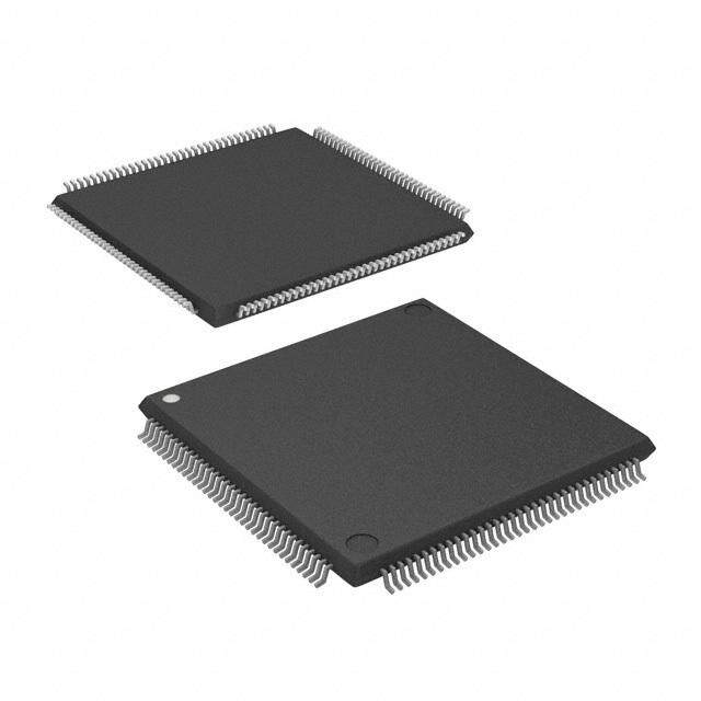
| 产品图片 |
|
| rohs | 符合RoHS无铅 / 符合限制有害物质指令(RoHS)规范要求 |
| 产品系列 | 嵌入式处理器和控制器,微控制器 - MCU,8位微控制器 -MCU,Microchip Technology PIC17C44-25/LPIC® 17C |
| 数据手册 | 点击此处下载产品Datasheet点击此处下载产品Datasheethttp://www.microchip.com/mymicrochip/filehandler.aspx?ddocname=en531149http://www.microchip.com/mymicrochip/filehandler.aspx?ddocname=en541028 |
| 产品型号 | PIC17C44-25/L |
| RAM容量 | 454 x 8 |
| 产品培训模块 | http://www.digikey.cn/PTM/IndividualPTM.page?site=cn&lang=zhs&ptm=2046http://www.digikey.cn/PTM/IndividualPTM.page?site=cn&lang=zhs&ptm=25053 |
| 产品种类 | 8位微控制器 -MCU |
| 供应商器件封装 | 44-PLCC(16.59x16.59) |
| 其它名称 | PIC17C4425L |
| 包装 | 管件 |
| 可编程输入/输出端数量 | 33 |
| 商标 | Microchip Technology |
| 处理器系列 | PIC17 |
| 外设 | POR,PWM,WDT |
| 安装风格 | SMD/SMT |
| 定时器数量 | 4 Timer |
| 封装 | Tube |
| 封装/外壳 | 44-LCC(J 形引线) |
| 封装/箱体 | PLCC-44 |
| 工作温度 | 0°C ~ 70°C |
| 工作电源电压 | 2.5 V to 6 V |
| 工厂包装数量 | 27 |
| 振荡器类型 | 外部 |
| 接口类型 | SCI, USART |
| 数据RAM大小 | 454 B |
| 数据Ram类型 | RAM |
| 数据ROM大小 | 454 B |
| 数据Rom类型 | EPROM |
| 数据总线宽度 | 8 bit |
| 数据转换器 | - |
| 最大工作温度 | + 70 C |
| 最大时钟频率 | 33 MHz |
| 最小工作温度 | 0 C |
| 标准包装 | 27 |
| 核心 | PIC |
| 核心处理器 | PIC |
| 核心尺寸 | 8-位 |
| 片上ADC | No |
| 片上DAC | Without DAC |
| 电压-电源(Vcc/Vdd) | 4.5 V ~ 6 V |
| 电源电压-最大 | 5.5 V |
| 电源电压-最小 | 4.5 V |
| 程序存储器大小 | 8 kB |
| 程序存储器类型 | EPROM |
| 程序存储容量 | 16KB(8K x 16) |
| 系列 | PIC17 |
| 输入/输出端数量 | 33 I/O |
| 连接性 | UART/USART |
| 速度 | 25MHz |
| 配用 | /product-detail/zh/AC164317/AC164317-ND/665646/product-detail/zh/DVA17XL441/DVA17XL441-ND/364786/product-detail/zh/PA17C42-PDZ/309-1007-ND/301881 |

.jpg)


- 商务部:美国ITC正式对集成电路等产品启动337调查
- 曝三星4nm工艺存在良率问题 高通将骁龙8 Gen1或转产台积电
- 太阳诱电将投资9.5亿元在常州建新厂生产MLCC 预计2023年完工
- 英特尔发布欧洲新工厂建设计划 深化IDM 2.0 战略
- 台积电先进制程称霸业界 有大客户加持明年业绩稳了
- 达到5530亿美元!SIA预计今年全球半导体销售额将创下新高
- 英特尔拟将自动驾驶子公司Mobileye上市 估值或超500亿美元
- 三星加码芯片和SET,合并消费电子和移动部门,撤换高东真等 CEO
- 三星电子宣布重大人事变动 还合并消费电子和移动部门
- 海关总署:前11个月进口集成电路产品价值2.52万亿元 增长14.8%


PDF Datasheet 数据手册内容提取
PIC17C4X High-Performance 8-Bit CMOS EPROM/ROM Microcontroller Devices included in this data sheet: Pin Diagram • PIC17CR42 PDIP, CERDIP, Windowed CERDIP • PIC17C42A VDD 1 40 RD0/AD8 • PIC17C43 RC0/AD0 2 39 RD1/AD9 RC1/AD1 3 38 RD2/AD10 • PIC17CR43 RC2/AD2 4 37 RD3/AD11 RC3/AD3 5 36 RD4/AD12 • PIC17C44 RC4/AD4 6 35 RD5/AD13 RC5/AD5 7 34 RD6/AD14 • PIC17C42† RRCC67//AADD67 89 PIC 3332 RMDC7L/RA/DV1P5P Microcontroller Core Features: VSS 10 17 31 VSS RB0/CAP1 11 C 30 RE0/ALE • Only 58 single word instructions to learn RB1/CAP2 12 4 29 RE1/OE RB2/PWM1 13 X 28 RE2/WR RB3/PWM2 14 27 TEST • All single cycle instructions (121 ns) except for RB4/TCLK12 15 26 RA0/INT program branches and table reads/writes which RB5/TCLK3 16 25 RA1/T0CKI RB6 17 24 RA2 are two-cycle RB7 18 23 RA3 OSC1/CLKIN 19 22 RA4/RX/DT • Operating speed: OSC2/CLKOUT 20 21 RA5/TX/CK O - DC - 33 MHz clock input - DC - 121 ns instruction cycle • TMR2: 8-bit timer/counter • TMR3: 16-bit timer/counter Program Memory Device Data Memory • Universal Synchronous Asynchronous Receiver EPROM ROM Transmitter (USART/SCI) PIC17CR42 - 2K 232 Special Microcontroller Features: PIC17C42A 2K - 232 • Power-on Reset (POR), Power-up Timer (PWRT) PIC17C43 4K - 454 and Oscillator Start-up Timer (OST) PIC17CR43 - 4K 454 • Watchdog Timer (WDT) with its own on-chip RC PIC17C44 8K - 454 oscillator for reliable operation PIC17C42† 2K - 232 • Code-protection O • Hardware Multiplier • Power saving SLEEP mode (Not available on the PIC17C42) • Selectable oscillator options • Interrupt capability CMOS Technology: • 16 levels deep hardware stack • Low-power, high-speed CMOS EPROM/ROM • Direct, indirect and relative addressing modes technology • Internal/External program memory execution • Fully static design • 64K x 16 addressable program memory space • Wide operating voltage range (2.5V to 6.0V) Peripheral Features: • Commercial and Industrial Temperature Range • 33 I/O pins with individual direction control • Low-power consumption • High current sink/source for direct LED drive - < 5 mA @ 5V, 4 MHz - RA2 and RA3 are open drain, high voltage - 100 m A typical @ 4.5V, 32 kHz (12V), high current (60 mA), I/O - < 1 m A typical standby current @ 5V • Two capture inputs and two PWM outputs - Captures are 16-bit, max resolution 160 ns - PWM resolution is 1- to 10-bit • TMR0: 16-bit timer/counter with 8-bit programma- ble prescaler • TMR1: 8-bit timer/counter †NOT recommended for new designs, use 17C42A. (cid:211) 1996 Microchip Technology Inc. DS30412C-page 1 ThisdocumentwascreatedwithFrameMaker404
PIC17C4X Pin Diagrams Cont.’d PLCC RC3/AD3RC2/AD2RC1/AD1RC0/AD0NCVDDVDDRD0/AD8RD1/AD9RD2/AD10RD3/AD11 MTQQFFPP A0/INTA1/T0CKIA2A3A4/RX/DTA5/TX/CKSC2/CLKOUTSC1/CLKINB7B6B5/TCLK3 RRRRRROORRR 6543214443424140 RC4/AD4 7 39 RD4/AD12 RC5/AD5 8 38 RD5/AD13 RC6/AD6 9 P 37 RD6/AD14 4443424140393837363534 RRBC0/7C/AAVVDPSS71SS 11110123 IC17C 33336543 RMVVSSDCSS7L/RA/DV1P5P RRREEE0T21/E/A/WOSLREET 1234 PIC 33333210 RRRRBBBB4321////TPPCCWWALPMMK22112 RRRBBB231//PP/CWWAMMP212 111456 4X 333210 RRREEE012///AOWLERE MCLR/VVVSSPSSP 567 17C 222987 VRVSSBSS0/CAP1 RB4/TCLK12 17 29 TEST RRDD76//AADD1154 89 4X 2265 RRCC76//AADD76 1819202122232425262728 RRDD54//AADD1132 1101 2243 RRCC54//AADD54 1213141516171819202122 RRROORRRRRR BBBSSAAAAAA 5/TCLK367C1/CLKINC2/CLKOUT5/TX/CK4/RX/DT321/T0CKI0/INT RD3/AD11RD2/AD10RD1/AD9RD0/AD8VDDVDDNCRC0/AD0RC1/AD1RC2/AD2RC3/AD3 All devices are available in all package types, listed in Section 21.0, with the following exceptions: • ROM devices are not available in Windowed CERDIP Packages • TQFP is not available for the PIC17C42. DS30412C-page 2 (cid:211) 1996 Microchip Technology Inc.
PIC17C4X Table of Contents 1.0 Overview..............................................................................................................................................................5 2.0 PIC17C4X Device Varieties.................................................................................................................................7 3.0 Architectural Overview.........................................................................................................................................9 4.0 Reset..................................................................................................................................................................15 5.0 Interrupts............................................................................................................................................................21 6.0 Memory Organization.........................................................................................................................................29 7.0 Table Reads and Table Writes...........................................................................................................................43 8.0 Hardware Multiplier............................................................................................................................................49 9.0 I/O Ports.............................................................................................................................................................53 10.0 Overview of Timer Resources............................................................................................................................65 11.0 Timer0................................................................................................................................................................67 12.0 Timer1, Timer2, Timer3, PWMs and Captures...................................................................................................71 13.0 Universal Synchronous Asynchronous Receiver Transmitter (USART) Module................................................83 14.0 Special Features of the CPU..............................................................................................................................99 15.0 Instruction Set Summary..................................................................................................................................107 16.0 Development Support.......................................................................................................................................143 17.0 PIC17C42 Electrical Characteristics................................................................................................................147 18.0 PIC17C42 DC and AC Characteristics.............................................................................................................163 19.0 PIC17CR42/42A/43/R43/44 Electrical Characteristics.....................................................................................175 20.0 PIC17CR42/42A/43/R43/44 DC and AC Characteristics.................................................................................193 21.0 Packaging Information......................................................................................................................................205 Appendix A: Modifications..........................................................................................................................................211 Appendix B: Compatibility...........................................................................................................................................211 Appendix C: What’s New............................................................................................................................................212 Appendix D: What’s Changed.....................................................................................................................................212 Appendix E: PIC16/17 Microcontrollers......................................................................................................................213 Appendix F: Errata for PIC17C42 Silicon...................................................................................................................223 Index............................................................................................................................................................................226 PIC17C4X Product Identification System....................................................................................................................237 For register and module descriptions in this data sheet, device legends show which devices apply to those sections. For example, the legend below shows that some features of only the PIC17C43, PIC17CR43, PIC17C44 are described in this section. Applicable Devices 42 R42 42A 43 R43 44 To Our Valued Customers We constantly strive to improve the quality of all our products and documentation. We have spent an excep- tional amount of time to ensure that these documents are correct. However, we realize that we may have missed a few things. If you find any information that is missing or appears in error from the previous version of the PIC17C4X Data Sheet (Literature Number DS30412B), please use the reader response form in the back of this data sheet to inform us. We appreciate your assistance in making this a better document. To assist you in the use of this document, Appendix C contains a list of new information in this data sheet, while Appendix D contains information that has changed (cid:211) 1996 Microchip Technology Inc. DS30412C-page 3
PIC17C4X NOTES: DS30412C-page 4 (cid:211) 1996 Microchip Technology Inc.
PIC17C4X 1.0 OVERVIEW power saving. The user can wake-up the chip from SLEEP through several external and internal interrupts This data sheet covers the PIC17C4X group of the and device resets. PIC17CXX family of microcontrollers. The following There are four configuration options for the device oper- devices are discussed in this data sheet: ational modes: • PIC17C42 • Microprocessor • PIC17CR42 • Microcontroller • PIC17C42A • Extended microcontroller • PIC17C43 • Protected microcontroller • PIC17CR43 The microprocessor and extended microcontroller • PIC17C44 modes allow up to 64K-words of external program The PIC17CR42, PIC17C42A, PIC17C43, memory. PIC17CR43, and PIC17C44 devices include architec- A highly reliable Watchdog Timer with its own on-chip tural enhancements over the PIC17C42. These RC oscillator provides protection against software mal- enhancements will be discussed throughout this data function. sheet. Table 1-1 lists the features of the PIC17C4X devices. The PIC17C4X devices are 40/44-Pin, EPROM/ROM-based members of the versatile A UV-erasable CERDIP-packaged version is ideal for PIC17CXX family of low-cost, high-performance, code development while the cost-effective One-Time CMOS, fully-static, 8-bit microcontrollers. Programmable (OTP) version is suitable for production in any volume. All PIC16/17 microcontrollers employ an advanced RISC architecture. The PIC17CXX has enhanced core The PIC17C4X fits perfectly in applications ranging features, 16-level deep stack, and multiple internal and from precise motor control and industrial process con- external interrupt sources. The separate instruction and trol to automotive, instrumentation, and telecom appli- data buses of the Harvard architecture allow a 16-bit cations. Other applications that require extremely fast wide instruction word with a separate 8-bit wide data. execution of complex software programs or the flexibil- The two stage instruction pipeline allows all instructions ity of programming the software code as one of the last to execute in a single cycle, except for program steps of the manufacturing process would also be well branches (which require two cycles). A total of 55 suited. The EPROM technology makes customization instructions (reduced instruction set) are available in of application programs (with unique security codes, the PIC17C42 and 58 instructions in all the other combinations, model numbers, parameter storage, devices. Additionally, a large register set gives some of etc.) fast and convenient. Small footprint package the architectural innovations used to achieve a very options make the PIC17C4X ideal for applications with high performance. For mathematical intensive applica- space limitations that require high performance. High tions all devices, except the PIC17C42, have a single speed execution, powerful peripheral features, flexible cycle 8 x 8 Hardware Multiplier. I/O, and low power consumption all at low cost make the PIC17C4X ideal for a wide range of embedded con- PIC17CXX microcontrollers typically achieve a 2:1 trol applications. code compression and a 4:1 speed improvement over other 8-bit microcontrollers in their class. 1.1 Family and Upward Compatibility PIC17C4X devices have up to 454 bytes of RAM and 33 I/O pins. In addition, the PIC17C4X adds several Those users familiar with the PIC16C5X and peripheral features useful in many high performance PIC16CXX families of microcontrollers will see the applications including: architectural enhancements that have been imple- mented. These enhancements allow the device to be • Four timer/counters more efficient in software and hardware requirements. • Two capture inputs Please refer to Appendix A for a detailed list of • Two PWM outputs enhancements and modifications. Code written for • A Universal Synchronous Asynchronous Receiver PIC16C5X or PIC16CXX can be easily ported to Transmitter (USART) PIC17CXX family of devices (Appendix B). These special features reduce external components, thus reducing cost, enhancing system reliability and 1.2 Development Support reducing power consumption. There are four oscillator options, of which the single pin RC oscillator provides a The PIC17CXX family is supported by a full-featured low-cost solution, the LF oscillator is for low frequency macro assembler, a software simulator, an in-circuit crystals and minimizes power consumption, XT is a emulator, a universal programmer, a “C” compiler, and standard crystal, and the EC is for external clock input. fuzzy logic support tools. The SLEEP (power-down) mode offers additional (cid:211) 1996 Microchip Technology Inc. DS30412C-page 5 ThisdocumentwascreatedwithFrameMaker404
PIC17C4X TABLE 1-1: PIC17CXX FAMILY OF DEVICES Features PIC17C42 PIC17CR42 PIC17C42A PIC17C43 PIC17CR43 PIC17C44 Maximum Frequency of Operation 25 MHz 33 MHz 33 MHz 33 MHz 33 MHz 33 MHz Operating Voltage Range 4.5 - 5.5V 2.5 - 6.0V 2.5 - 6.0V 2.5 - 6.0V 2.5 - 6.0V 2.5 - 6.0V Program Memory x16 (EPROM) 2K - 2K 4K - 8K (ROM) - 2K - - 4K - Data Memory (bytes) 232 232 232 454 454 454 Hardware Multiplier (8 x 8) - Yes Yes Yes Yes Yes Timer0 (16-bit + 8-bit postscaler) Yes Yes Yes Yes Yes Yes Timer1 (8-bit) Yes Yes Yes Yes Yes Yes Timer2 (8-bit) Yes Yes Yes Yes Yes Yes Timer3 (16-bit) Yes Yes Yes Yes Yes Yes Capture inputs (16-bit) 2 2 2 2 2 2 PWM outputs (up to 10-bit) 2 2 2 2 2 2 USART/SCI Yes Yes Yes Yes Yes Yes Power-on Reset Yes Yes Yes Yes Yes Yes Watchdog Timer Yes Yes Yes Yes Yes Yes External Interrupts Yes Yes Yes Yes Yes Yes Interrupt Sources 11 11 11 11 11 11 Program Memory Code Protect Yes Yes Yes Yes Yes Yes I/O Pins 33 33 33 33 33 33 I/O High Current Capabil- Source 25 mA 25 mA 25 mA 25 mA 25 mA 25 mA ity Sink 25 mA(1) 25 mA(1) 25 mA(1) 25 mA(1) 25 mA(1) 25 mA(1) Package Types 40-pin DIP 40-pin DIP 40-pin DIP 40-pin DIP 40-pin DIP 40-pin DIP 44-pin PLCC 44-pin PLCC 44-pin PLCC 44-pin PLCC 44-pin PLCC 44-pin PLCC 44-pin MQFP 44-pin MQFP 44-pin MQFP 44-pin MQFP 44-pin MQFP 44-pin MQFP 44-pin TQFP 44-pin TQFP 44-pin TQFP 44-pin TQFP 44-pin TQFP Note 1: Pins RA2 and RA3 can sink up to 60 mA. DS30412C-page 6 (cid:211) 1996 Microchip Technology Inc.
PIC17C4X 2.0 PIC17C4X DEVICE VARIETIES 2.3 Quick-Turnaround-Production (QTP) Devices A variety of frequency ranges and packaging options are available. Depending on application and production Microchip offers a QTP Programming Service for fac- requirements, the proper device option can be selected tory production orders. This service is made available using the information in the PIC17C4X Product Selec- for users who choose not to program a medium to high tion System section at the end of this data sheet. When quantity of units and whose code patterns have stabi- placing orders, please use the “PIC17C4X Product lized. The devices are identical to the OTP devices but Identification System” at the back of this data sheet to with all EPROM locations and configuration options specify the correct part number. already programmed by the factory. Certain code and For the PIC17C4X family of devices, there are four prototype verification procedures apply before produc- device “types” as indicated in the device number: tion shipments are available. Please contact your local Microchip Technology sales office for more details. 1. C, as in PIC17C42. These devices have EPROM type memory and operate over the 2.4 Serialized Quick-Turnaround standard voltage range. Production (SQTPSM) Devices 2. LC, as in PIC17LC42. These devices have EPROM type memory, operate over an Microchip offers a unique programming service where extended voltage range, and reduced frequency a few user-defined locations in each device are pro- range. grammed with different serial numbers. The serial num- 3. CR, as in PIC17CR42. These devices have bers may be random, pseudo-random or sequential. ROM type memory and operate over the stan- Serial programming allows each device to have a dard voltage range. unique number which can serve as an entry-code, 4. LCR, as in PIC17LCR42. These devices have password or ID number. ROM type memory, operate over an extended ROM devices do not allow serialization information in voltage range, and reduced frequency range. the program memory space. 2.1 UV Erasable Devices For information on submitting ROM code, please con- tact your regional sales office. The UV erasable version, offered in CERDIP package, is optimal for prototype development and pilot pro- 2.5 Read Only Memory (ROM) Devices grams. Microchip offers masked ROM versions of several of The UV erasable version can be erased and repro- the highest volume parts, thus giving customers a low grammed to any of the configuration modes. cost option for high volume, mature products. Microchip's PRO MATE(cid:228) programmer supports pro- gramming of the PIC17C4X. Third party programmers For information on submitting ROM code, please con- also are available; refer to the Third Party Guide for a tact your regional sales office. list of sources. 2.2 One-Time-Programmable (OTP) Devices The availability of OTP devices is especially useful for customers expecting frequent code changes and updates. The OTP devices, packaged in plastic packages, per- mit the user to program them once. In addition to the program memory, the configuration bits must also be programmed. (cid:211) 1996 Microchip Technology Inc. DS30412C-page 7 ThisdocumentwascreatedwithFrameMaker404
PIC17C4X NOTES: DS30412C-page 8 (cid:211) 1996 Microchip Technology Inc.
PIC17C4X 3.0 ARCHITECTURAL OVERVIEW The PIC17CXX devices contain an 8-bit ALU and work- ing register. The ALU is a general purpose arithmetic The high performance of the PIC17C4X can be attrib- unit. It performs arithmetic and Boolean functions uted to a number of architectural features commonly between data in the working register and any register found in RISC microprocessors. To begin with, the file. PIC17C4X uses a modified Harvard architecture. This The ALU is 8-bits wide and capable of addition, sub- architecture has the program and data accessed from traction, shift, and logical operations. Unless otherwise separate memories. So the device has a program mentioned, arithmetic operations are two's comple- memory bus and a data memory bus. This improves ment in nature. bandwidth over traditional von Neumann architecture, where program and data are fetched from the same The WREG register is an 8-bit working register used for memory (accesses over the same bus). Separating ALU operations. program and data memory further allows instructions to All PIC17C4X devices (except the PIC17C42) have an be sized differently than the 8-bit wide data word. 8 x 8 hardware multiplier. This multiplier generates a PIC17C4X opcodes are 16-bits wide, enabling single 16-bit result in a single cycle. word instructions. The full 16-bit wide program memory bus fetches a 16-bit instruction in a single cycle. A two- Depending on the instruction executed, the ALU may stage pipeline overlaps fetch and execution of instruc- affect the values of the Carry (C), Digit Carry (DC), and tions. Consequently, all instructions execute in a single Zero (Z) bits in the STATUS register. The C and DC bits cycle (121 ns @ 33 MHz), except for program branches operate as a borrow and digit borrow out bit, respec- and two special instructions that transfer data between tively, in subtraction. See the SUBLW and SUBWF program and data memory. instructions for examples. The PIC17C4X can address up to 64K x 16 of program Although the ALU does not perform signed arithmetic, memory space. the Overflow bit (OV) can be used to implement signed math. Signed arithmetic is comprised of a magnitude The PIC17C42 and PIC17C42A integrate 2K x 16 of and a sign bit. The overflow bit indicates if the magni- EPROM program memory on-chip, while the tude overflows and causes the sign bit to change state. PIC17CR42 has 2K x 16 of ROM program memory on- Signed math can have greater than 7-bit values (mag- chip. nitude), if more than one byte is used. The use of the The PIC17C43 integrates 4K x 16 of EPROM program overflow bit only operates on bit6 (MSb of magnitude) memory, while the PIC17CR43 has 4K x 16 of ROM and bit7 (sign bit) of the value in the ALU. That is, the program memory. overflow bit is not useful if trying to implement signed The PIC17C44 integrates 8K x 16 EPROM program math where the magnitude, for example, is 11-bits. If memory. the signed math values are greater than 7-bits (15-, 24- or 31-bit), the algorithm must ensure that the low order Program execution can be internal only (microcontrol- bytes ignore the overflow status bit. ler or protected microcontroller mode), external only (microprocessor mode) or both (extended microcon- Care should be taken when adding and subtracting troller mode). Extended microcontroller mode does not signed numbers to ensure that the correct operation is allow code protection. executed. Example 3-1 shows an item that must be taken into account when doing signed arithmetic on an The PIC17CXX can directly or indirectly address its ALU which operates as an unsigned machine. register files or data memory. All special function regis- ters, including the Program Counter (PC) and Working EXAMPLE 3-1: SIGNED MATH Register (WREG), are mapped in the data memory. The PIC17CXX has an orthogonal (symmetrical) Hex Value Signed Value Unsigned Value instruction set that makes it possible to carry out any Math Math operation on any register using any addressing mode. FFh -127 255 This symmetrical nature and lack of ‘special optimal sit- + 01h + 1 + 1 uations’ make programming with the PIC17CXX simple = ? = -126 (FEh) = 0 (00h); yet efficient. In addition, the learning curve is reduced Carry bit = 1 significantly. Signed math requires the result in REG to One of the PIC17CXX family architectural enhance- be FEh (-126). This would be accomplished ments from the PIC16CXX family allows two file regis- by subtracting one as opposed to adding ters to be used in some two operand instructions. This one. allows data to be moved directly between two registers Simplified block diagrams are shown in Figure 3-1 and without going through the WREG register. This Figure 3-2. The descriptions of the device pins are increases performance and decreases program mem- listed in Table 3-1. ory usage. (cid:211) 1996 Microchip Technology Inc. DS30412C-page 9 ThisdocumentwascreatedwithFrameMaker404
PIC17C4X FIGURE 3-1: PIC17C42 BLOCK DIAGRAM AD <15:0>PORTC and PORTD ALE, WR, OEPORTE OSC1, OSC2 , VVDDSS MCLR/VPP TEST E D O C IR BUS <16> IR LATCH <16> INSTRUCTION8DECODER8 FSR0CONTROL OUTPUTSDEFSR1 ROM LATCH <16>BLE LATCH <16>8 DATA LATCH PROGRAMMEMORYSYSTEM(EPROM/ROM)BUS2K x 16TABLE PTR<16>INTER-FACE PCL 16ADDRESS LATCH 11STACK16 x 1616 16 Q1, Q2, Q3, Q4 CLOCK GENERATORPOWER ON RESETCONTROLWATCHDOG TIMERCHIP_RESETSIGNALSOSC STARTUP TIMERAND OTHERTO CPUTEST MODE SELECT CONTROLSIGNALS A T > LITERAL PCLATH<8 PCH RUPTULE RD EO TM N I > > 7:0 3 2:0 8IR BUS < M ADDR BUFFER DATA RAM232x8 DATA LATCH BSR 4 7>IR < >8< SUB ATAD RA R < I S READ/WRITEDECODEEG <8>FOR REGISTERMAPPEDIN DATA SPACE WRFRDF DATA BUS <8> mer1, Timer2, Timer3CAPTUREPWM DIGITAL I/OPORTS A, B SERIAL PORT Timer0 MODULE PERIPHERALS RA1/T0CKI RA0/INT WR Ti > 6 1 < IR BUS OP R 6 8 6 2 RA1/T0CKI T E BI LU FT A HI S 8 6 PORTB RB0/CAP1RB1/CAP2RB2/PWM1RB2/PWM2RB4/TCLK12RB5/TCLK3RB6RB7 PORTA RA0/INTRA1/T0CKIRA2RA3RA4/RX/DTRA5/TX/CK DS30412C-page 10 (cid:211) 1996 Microchip Technology Inc.
PIC17C4X FIGURE 3-2: PIC17CR42/42A/43/R43/44 BLOCK DIAGRAM E AD <15:0>PORTC andPORTD LE, WR, OEPORTE OSC1, OSC2 , VVDDSS MCLR/VPP TEST D A O C IR BUS <16> IR LATCH <16> INSTRUCTION8DECODER8 FSR0CONTROL OUTPUTSDEFSR1 ROM LATCH <16>BLE LATCH <16>8 DATA LATCH PROGRAMMEMORY(EPROM/ROM)SYSTEM2K x 16 - PIC17CR42BUS2K x 16 - PIC17C42ATABLE PTR<16>INTER-4K x 16 - PIC17C43FACE4K x 16 - PIC17CR438K x 16 - PIC17C44PCL 16ADDRESS LATCH 13STACK16 x 1616 16 Q1, Q2, Q3, Q4 CLOCK GENERATORPOWER ON RESETCONTROLWATCHDOG TIMERCHIP_RESETSIGNALSOSC STARTUP TIMERAND OTHERTO CPUTEST MODE SELECT CONTROLSIGNALS A T > LITERAL PCLATH<8 PCH RUPTULE RD EO TM N I BSR<7:4>12IR BUS<7:0> RAM ADDR BUFFER DATA RAM 232 x 8 PIC17CR42232 x 8 PIC17C42A454 x 8 PIC17C43454 x 8 PIC17CR43454 x 8 PIC17C44 DATA LATCH BSR 43 R <7>IR <2:0> >8< SUB ATAD I S READ/WRITEDECODEFOR REGISTERMAPPEDIN DATA SPACE ultWRFRDF PRODL DATA BUS <8> mer1, Timer2, Timer3CAPTUREPWM DIGITAL I/OPORTS A, B SERIAL PORT Timer0 MODULE PERIPHERALS RA1/T0CKI RA0/INT m Ti R BUS <16> REG <8> 8 x 8 PRODH 6 8 6 2 RA1/T0CKI I W BITOP ALU HIFTER 8 6 S PORTB RB0/CAP1RB1/CAP2RB2/PWM1RB2/PWM2RB4/TCLK12RB5/TCLK3RB6RB7 PORTA RA0/INTRA1/T0CKIRA2RA3RA4/RX/DTRA5/TX/CK (cid:211) 1996 Microchip Technology Inc. DS30412C-page 11
PIC17C4X TABLE 3-1: PINOUT DESCRIPTIONS DIP PLCC QFP I/O/P Buffer Name Description No. No. No. Type Type OSC1/CLKIN 19 21 37 I ST Oscillator input in crystal/resonator or RC oscillator mode. External clock input in external clock mode. OSC2/CLKOUT 20 22 38 O — Oscillator output. Connects to crystal or resonator in crystal oscillator mode. In RC oscillator or external clock modes OSC2 pin outputs CLKOUT which has one fourth the fre- quency of OSC1 and denotes the instruction cycle rate. MCLR/VPP 32 35 7 I/P ST Master clear (reset) input/Programming Voltage (VPP) input. This is the active low reset input to the chip. PORTA is a bi-directional I/O Port except for RA0 and RA1 which are input only. RA0/INT 26 28 44 I ST RA0/INT can also be selected as an external interrupt input. Interrupt can be configured to be on positive or negative edge. RA1/T0CKI 25 27 43 I ST RA1/T0CKI can also be selected as an external interrupt input, and the interrupt can be configured to be on posi- tive or negative edge. RA1/T0CKI can also be selected to be the clock input to the Timer0 timer/counter. RA2 24 26 42 I/O ST High voltage, high current, open drain input/output port pins. RA3 23 25 41 I/O ST High voltage, high current, open drain input/output port pins. RA4/RX/DT 22 24 40 I/O ST RA4/RX/DT can also be selected as the USART (SCI) Asynchronous Receive or USART (SCI) Synchronous Data. RA5/TX/CK 21 23 39 I/O ST RA5/TX/CK can also be selected as the USART (SCI) Asynchronous Transmit or USART (SCI) Synchronous Clock. PORTB is a bi-directional I/O Port with software configurable weak pull-ups. RB0/CAP1 11 13 29 I/O ST RB0/CAP1 can also be the CAP1 input pin. RB1/CAP2 12 14 30 I/O ST RB1/CAP2 can also be the CAP2 input pin. RB2/PWM1 13 15 31 I/O ST RB2/PWM1 can also be the PWM1 output pin. RB3/PWM2 14 16 32 I/O ST RB3/PWM2 can also be the PWM2 output pin. RB4/TCLK12 15 17 33 I/O ST RB4/TCLK12 can also be the external clock input to Timer1 and Timer2. RB5/TCLK3 16 18 34 I/O ST RB5/TCLK3 can also be the external clock input to Timer3. RB6 17 19 35 I/O ST RB7 18 20 36 I/O ST PORTC is a bi-directional I/O Port. RC0/AD0 2 3 19 I/O TTL This is also the lower half of the 16-bit wide system bus RC1/AD1 3 4 20 I/O TTL in microprocessor mode or extended microcontroller mode. In multiplexed system bus configuration, these RC2/AD2 4 5 21 I/O TTL pins are address output as well as data input or output. RC3/AD3 5 6 22 I/O TTL RC4/AD4 6 7 23 I/O TTL RC5/AD5 7 8 24 I/O TTL RC6/AD6 8 9 25 I/O TTL RC7/AD7 9 10 26 I/O TTL Legend: I = Input only; O = Output only; I/O = Input/Output; P = Power; — = Not Used; TTL = TTL input; ST = Schmitt Trigger input. DS30412C-page 12 (cid:211) 1996 Microchip Technology Inc.
PIC17C4X TABLE 3-1: PINOUT DESCRIPTIONS DIP PLCC QFP I/O/P Buffer Name Description No. No. No. Type Type PORTD is a bi-directional I/O Port. RD0/AD8 40 43 15 I/O TTL This is also the upper byte of the 16-bit system bus in RD1/AD9 39 42 14 I/O TTL microprocessor mode or extended microprocessor mode or extended microcontroller mode. In multiplexed system RD2/AD10 38 41 13 I/O TTL bus configuration these pins are address output as well RD3/AD11 37 40 12 I/O TTL as data input or output. RD4/AD12 36 39 11 I/O TTL RD5/AD13 35 38 10 I/O TTL RD6/AD14 34 37 9 I/O TTL RD7/AD15 33 36 8 I/O TTL PORTE is a bi-directional I/O Port. RE0/ALE 30 32 4 I/O TTL In microprocessor mode or extended microcontroller mode, it is the Address Latch Enable (ALE) output. Address should be latched on the falling edge of ALE output. RE1/OE 29 31 3 I/O TTL In microprocessor or extended microcontroller mode, it is the Output Enable (OE) control output (active low). RE2/WR 28 30 2 I/O TTL In microprocessor or extended microcontroller mode, it is the Write Enable (WR) control output (active low). TEST 27 29 1 I ST Test mode selection control input. Always tie to VSS for nor- mal operation. VSS 10, 11, 5, 6, P Ground reference for logic and I/O pins. 31 12, 27, 28 33, 34 VDD 1 1, 44 16, 17 P Positive supply for logic and I/O pins. Legend: I = Input only; O = Output only; I/O = Input/Output; P = Power; — = Not Used; TTL = TTL input; ST = Schmitt Trigger input. (cid:211) 1996 Microchip Technology Inc. DS30412C-page 13
PIC17C4X 3.1 Clocking Scheme/Instruction Cycle 3.2 Instruction Flow/Pipelining The clock input (from OSC1) is internally divided by An “Instruction Cycle” consists of four Q cycles (Q1, four to generate four non-overlapping quadrature Q2, Q3, and Q4). The instruction fetch and execute are clocks, namely Q1, Q2, Q3, and Q4. Internally, the pro- pipelined such that fetch takes one instruction cycle gram counter (PC) is incremented every Q1, and the while decode and execute takes another instruction instruction is fetched from the program memory and cycle. However, due to the pipelining, each instruction latched into the instruction register in Q4. The instruc- effectively executes in one cycle. If an instruction tion is decoded and executed during the following Q1 causes the program counter to change (e.g. GOTO) then through Q4. The clocks and instruction execution flow two cycles are required to complete the instruction are shown in Figure 3-3. (Example 3-2). A fetch cycle begins with the program counter incre- menting in Q1. In the execution cycle, the fetched instruction is latched into the “Instruction Register (IR)” in cycle Q1. This instruction is then decoded and executed during the Q2, Q3, and Q4 cycles. Data memory is read during Q2 (operand read) and written during Q4 (destination write). FIGURE 3-3: CLOCK/INSTRUCTION CYCLE Q1 Q2 Q3 Q4 Q1 Q2 Q3 Q4 Q1 Q2 Q3 Q4 OSC1 Q1 Q2 Internal Q3 phase clock Q4 PC PC PC+1 PC+2 OSC2/CLKOUT (RC mode) Fetch INST (PC) Execute INST (PC-1) Fetch INST (PC+1) Execute INST (PC) Fetch INST (PC+2) Execute INST (PC+1) EXAMPLE 3-2: INSTRUCTION PIPELINE FLOW Tcy0 Tcy1 Tcy2 Tcy3 Tcy4 Tcy5 1. MOVLW 55h Fetch 1 Execute 1 2. MOVWF PORTB Fetch 2 Execute 2 3. CALL SUB_1 Fetch 3 Execute 3 4. BSF PORTA, BIT3 (Forced NOP) Fetch 4 Flush 5. Instruction @ address SUB_1 Fetch SUB_1 Execute SUB_1 All instructions are single cycle, except for any program branches. These take two cycles since the fetch instruction is “flushed” from the pipeline while the new instruction is being fetched and then executed. DS30412C-page 14 (cid:211) 1996 Microchip Technology Inc.
PIC17C4X 4.0 RESET 4.1 Power-on Reset (POR), Power-up Timer (PWRT), and Oscillator Start-up The PIC17CXX differentiates between various kinds of Timer (OST) reset: • Power-on Reset (POR) 4.1.1 POWER-ON RESET (POR) • MCLR reset during normal operation The Power-on Reset circuit holds the device in reset • WDT Reset (normal operation) until VDD is above the trip point (in the range of 1.4V - Some registers are not affected in any reset condition; 2.3V). The PIC17C42 does not produce an internal their status is unknown on POR and unchanged in any reset when VDD declines. All other devices will produce other reset. Most other registers are forced to a “reset an internal reset for both rising and falling VDD. To take state” on Power-on Reset (POR), on MCLR or WDT advantage of the POR, just tie the MCLR/VPP pin Reset and on MCLR reset during SLEEP. They are not directly (or through a resistor) to VDD. This will eliminate affected by a WDT Reset during SLEEP, since this reset external RC components usually needed to create is viewed as the resumption of normal operation. The Power-on Reset. A minimum rise time for VDD is TO and PD bits are set or cleared differently in different required. See Electrical Specifications for details. reset situations as indicated in Table 4-3. These bits are used in software to determine the nature of reset. See 4.1.2 POWER-UP TIMER (PWRT) Table 4-4 for a full description of reset states of all reg- The Power-up Timer provides a fixed 96 ms time-out isters. (nominal) on power-up. This occurs from rising edge of Note: While the device is in a reset state, the the POR signal and after the first rising edge of MCLR internal phase clock is held in the Q1 state. (detected high). The Power-up Timer operates on an Any processor mode that allows external internal RC oscillator. The chip is kept in RESET as execution will force the RE0/ALE pin as a long as the PWRT is active. In most cases the PWRT low output and the RE1/OE and RE2/WR delay allows the VDD to rise to an acceptable level. pins as high outputs. The power-up time delay will vary from chip to chip and A simplified block diagram of the on-chip reset circuit is to VDD and temperature. See DC parameters for shown in Figure 4-1. details. FIGURE 4-1: SIMPLIFIED BLOCK DIAGRAM OF ON-CHIP RESET CIRCUIT External Reset MCLR WDT WDT Module Time_Out Reset VDD rise detect S Power_On_Reset VDD OST/PWRT Chip_Reset OST R Q 10-bit Ripple counter OSC1 PWRT On-chip RC OSC† 10-bit Ripple counter T R W P Power_Up OST able (oEnnlya bdluer itnhge PPoWwRerT_ Utimp)er e n bl E a (Power_Up + Wake_Up) (XT + LF) n E (Enable the OST if it is Power_Up or Wake_Up † This RC oscillator is shared with the WDT from SLEEP and OSC type is XT or LF) when not in a power-up sequence. (cid:211) 1996 Microchip Technology Inc. DS30412C-page 15 ThisdocumentwascreatedwithFrameMaker404
PIC17C4X 4.1.3 OSCILLATOR START-UP TIMER (OST) TABLE 4-1: TIME-OUT IN VARIOUS SITUATIONS The Oscillator Start-up Timer (OST) provides a 1024 oscillator cycle (1024TOSC) delay after MCLR is Oscillator Power-up Wake up MCLR detected high or a wake-up from SLEEP event occurs. Configuration from Reset The OST time-out is invoked only for XT and LF oscilla- SLEEP tor modes on a Power-on Reset or a Wake-up from XT, LF Greater of: 1024TOSC — SLEEP. 96 ms or The OST counts the oscillator pulses on the 1024TOSC OSC1/CLKIN pin. The counter only starts incrementing EC, RC Greater of: — — after the amplitude of the signal reaches the oscillator 96 ms or input thresholds. This delay allows the crystal oscillator 1024TOSC or resonator to stabilize before the device exits reset. The length of time-out is a function of the crystal/reso- The time-out sequence begins from the first rising edge nator frequency. of MCLR. 4.1.4 TIME-OUT SEQUENCE Table 4-3 shows the reset conditions for some special registers, while Table 4-4 shows the initialization condi- On power-up the time-out sequence is as follows: First tions for all the registers. The shaded registers (in the internal POR signal goes high when the POR trip Table 4-4) are for all devices except the PIC17C42. In point is reached. If MCLR is high, then both the OST the PIC17C42, the PRODH and PRODL registers are and PWRT timers start. In general the PWRT time-out general purpose RAM. is longer, except with low frequency crystals/resona- TABLE 4-2: STATUS BITS AND THEIR tors. The total time-out also varies based on oscillator SIGNIFICANCE configuration. Table 4-1 shows the times that are asso- ciated with the oscillator configuration. Figure 4-2 and TO PD Event Figure 4-3 display these time-out sequences. If the device voltage is not within electrical specification 1 1 Power-on Reset, MCLR Reset during normal at the end of a time-out, the MCLR/VPP pin must be operation, or CLRWDT instruction executed held low until the voltage is within the device specifica- 1 0 MCLR Reset during SLEEP or interrupt wake-up tion. The use of an external RC delay is sufficient for from SLEEP many of these applications. 0 1 WDT Reset during normal operation 0 0 WDT Reset during SLEEP In Figure 4-2, Figure 4-3 and Figure 4-4, TPWRT > TOST, as would be the case in higher frequency crys- tals. For lower frequency crystals, (i.e., 32 kHz) TOST would be greater. TABLE 4-3: RESET CONDITION FOR THE PROGRAM COUNTER AND THE CPUSTA REGISTER Event PCH:PCL CPUSTA OST Active Power-on Reset 0000h --11 11-- Yes MCLR Reset during normal operation 0000h --11 11-- No MCLR Reset during SLEEP 0000h --11 10-- Yes (2) WDT Reset during normal operation 0000h --11 01-- No WDT Reset during SLEEP (3) 0000h --11 00-- Yes (2) Interrupt wake-up from SLEEP GLINTD is set PC + 1 --11 10-- Yes (2) GLINTD is clear PC + 1 (1) --10 10-- Yes (2) Legend: u = unchanged, x = unknown, - = unimplemented read as '0'. Note 1: On wake-up, this instruction is executed. The instruction at the appropriate interrupt vector is fetched and then executed. 2: The OST is only active when the Oscillator is configured for XT or LF modes. 3: The Program Counter = 0, that is the device branches to the reset vector. This is different from the mid-range devices. DS30412C-page 16 (cid:211) 1996 Microchip Technology Inc.
PIC17C4X FIGURE 4-2: TIME-OUT SEQUENCE ON POWER-UP (MCLR TIED TO VDD) VDD MCLR INTERNAL POR TPWRT PWRT TIME-OUT TOST OST TIME-OUT INTERNAL RESET FIGURE 4-3: TIME-OUT SEQUENCE ON POWER-UP (MCLR NOT TIED TO VDD) VDD MCLR INTERNAL POR TPWRT PWRT TIME-OUT TOST OST TIME-OUT INTERNAL RESET FIGURE 4-4: SLOW RISE TIME (MCLR TIED TO VDD) 5V VDD 0V 1V MCLR INTERNAL POR TPWRT PWRT TIME-OUT TOST OST TIME-OUT INTERNAL RESET (cid:211) 1996 Microchip Technology Inc. DS30412C-page 17
PIC17C4X FIGURE 4-5: OSCILLATOR START-UP TIME FIGURE 4-8: PIC17C42 EXTERNAL POWER-ON RESET CIRCUIT (FOR SLOW VDD POWER-UP) VDD VDD VDD MCLR D R OSC2 R1 MCLR TOSC1 C PIC17C42 TOST OST TIME_OUT PWRT TIME_OUT Note 1: An external Power-on Reset circuit is TPWRT required only if VDD power-up time is too INTERNAL RESET slow. The diode D helps discharge the This figure shows in greater detail the timings involved capacitor quickly when VDD powers with the oscillator start-up timer. In this example the down. low frequency crystal start-up time is larger than power-up time (TPWRT). 2: R < 40 kW is recommended to ensure Tosc1 = time for the crystal oscillator to react to an that the voltage drop across R does not oscillation level detectable by the Oscillator Start-up exceed 0.2V (max. leakage current spec. Timer (ost). TOST = 1024TOSC. on the MCLR/VPP pin is 5 m A). A larger voltage drop will degrade VIH level on the FIGURE 4-6: USING ON-CHIP POR MCLR/VPP pin. 3: R1 = 100W to 1 kW will limit any current VDD flowing into MCLR from external capaci- VDD tor C in the event of MCLR/VPP pin breakdown due to Electrostatic Dis- MCLR charge (ESD) or (Electrical Overstress) EOS. PIC17CXX FIGURE 4-9: BROWN-OUT PROTECTION CIRCUIT 2 FIGURE 4-7: BROWN-OUT PROTECTION CIRCUIT 1 VDD VDD R1 VDD Q1 VDD MCLR 33k R2 40 kW PIC17CXX 10k MCLR 40 kW PIC17CXX This brown-out circuit is less expensive, albeit less accurate. Transistor Q1 turns off when VDD is below a certain level such that: T(Vhzis + c 0ir.c7uVit) wwilhl earcet iVvazt e= rZeesneet rw vhoeltna gVeD.D goes below VDD • R1R +1 R2 = 0.7V DS30412C-page 18 (cid:211) 1996 Microchip Technology Inc.
PIC17C4X T A BLE 4-4: INITIALIZATION CONDITIONS FOR SPECIAL FUNCTION REGISTERS MCLR Reset Wake-up from SLEEP Register Address Power-on Reset WDT Reset through interrupt Unbanked INDF0 00h 0000 0000 0000 0000 0000 0000 FSR0 01h xxxx xxxx uuuu uuuu uuuu uuuu PCL 02h 0000h 0000h PC + 1(2) PCLATH 03h 0000 0000 0000 0000 uuuu uuuu ALUSTA 04h 1111 xxxx 1111 uuuu 1111 uuuu T0STA 05h 0000 000- 0000 000- 0000 000- CPUSTA(3) 06h --11 11-- --11 qq-- --uu qq-- INTSTA 07h 0000 0000 0000 0000 uuuu uuuu(1) INDF1 08h 0000 0000 0000 0000 uuuu uuuu FSR1 09h xxxx xxxx uuuu uuuu uuuu uuuu WREG 0Ah xxxx xxxx uuuu uuuu uuuu uuuu TMR0L 0Bh xxxx xxxx uuuu uuuu uuuu uuuu TMR0H 0Ch xxxx xxxx uuuu uuuu uuuu uuuu TBLPTRL (4) 0Dh xxxx xxxx uuuu uuuu uuuu uuuu TBLPTRH (4) 0Eh xxxx xxxx uuuu uuuu uuuu uuuu TBLPTRL (5) 0Dh 0000 0000 0000 0000 uuuu uuuu TBLPTRH (5) 0Eh 0000 0000 0000 0000 uuuu uuuu BSR 0Fh 0000 0000 0000 0000 uuuu uuuu Bank 0 PORTA 10h 0-xx xxxx 0-uu uuuu uuuu uuuu DDRB 11h 1111 1111 1111 1111 uuuu uuuu PORTB 12h xxxx xxxx uuuu uuuu uuuu uuuu RCSTA 13h 0000 -00x 0000 -00u uuuu -uuu RCREG 14h xxxx xxxx uuuu uuuu uuuu uuuu TXSTA 15h 0000 --1x 0000 --1u uuuu --uu TXREG 16h xxxx xxxx uuuu uuuu uuuu uuuu SPBRG 17h xxxx xxxx uuuu uuuu uuuu uuuu Bank 1 DDRC 10h 1111 1111 1111 1111 uuuu uuuu PORTC 11h xxxx xxxx uuuu uuuu uuuu uuuu DDRD 12h 1111 1111 1111 1111 uuuu uuuu PORTD 13h xxxx xxxx uuuu uuuu uuuu uuuu DDRE 14h ---- -111 ---- -111 ---- -uuu PORTE 15h ---- -xxx ---- -uuu ---- -uuu PIR 16h 0000 0010 0000 0010 uuuu uuuu(1) PIE 17h 0000 0000 0000 0000 uuuu uuuu Legend: u = unchanged, x = unknown, - = unimplemented read as '0', q = value depends on condition. Note 1: One or more bits in INTSTA, PIR will be affected (to cause wake-up). 2: When the wake-up is due to an interrupt and the GLINTD bit is cleared, the PC is loaded with the interrupt vector. 3: See Table 4-3 for reset value of specific condition. 4: Only applies to the PIC17C42. 5: Does not apply to the PIC17C42. (cid:211) 1996 Microchip Technology Inc. DS30412C-page 19
PIC17C4X TABLE 4-4: INITIALIZATION CONDITIONS FOR SPECIAL FUNCTION REGISTERS (Cont.’d) MCLR Reset Wake-up from SLEEP Register Address Power-on Reset WDT Reset through interrupt Bank 2 TMR1 10h xxxx xxxx uuuu uuuu uuuu uuuu TMR2 11h xxxx xxxx uuuu uuuu uuuu uuuu TMR3L 12h xxxx xxxx uuuu uuuu uuuu uuuu TMR3H 13h xxxx xxxx uuuu uuuu uuuu uuuu PR1 14h xxxx xxxx uuuu uuuu uuuu uuuu PR2 15h xxxx xxxx uuuu uuuu uuuu uuuu PR3/CA1L 16h xxxx xxxx uuuu uuuu uuuu uuuu PR3/CA1H 17h xxxx xxxx uuuu uuuu uuuu uuuu Bank 3 PW1DCL 10h xx-- ---- uu-- ---- uu-- ---- PW2DCL 11h xx-- ---- uu-- ---- uu-- ---- PW1DCH 12h xxxx xxxx uuuu uuuu uuuu uuuu PW2DCH 13h xxxx xxxx uuuu uuuu uuuu uuuu CA2L 14h xxxx xxxx uuuu uuuu uuuu uuuu CA2H 15h xxxx xxxx uuuu uuuu uuuu uuuu TCON1 16h 0000 0000 0000 0000 uuuu uuuu TCON2 17h 0000 0000 0000 0000 uuuu uuuu Unbanked PRODL (5) 18h xxxx xxxx uuuu uuuu uuuu uuuu PRODH (5) 19h xxxx xxxx uuuu uuuu uuuu uuuu Legend: u = unchanged, x = unknown, - = unimplemented read as '0', q = value depends on condition. Note 1: One or more bits in INTSTA, PIR will be affected (to cause wake-up). 2: When the wake-up is due to an interrupt and the GLINTD bit is cleared, the PC is loaded with the interrupt vector. 3: See Table 4-3 for reset value of specific condition. 4: Only applies to the PIC17C42. 5: Does not apply to the PIC17C42. DS30412C-page 20 (cid:211) 1996 Microchip Technology Inc.
PIC17C4X 5.0 INTERRUPTS When an interrupt is responded to, the GLINTD bit is automatically set to disable any further interrupt, the The PIC17C4X devices have 11 sources of interrupt: return address is pushed onto the stack and the PC is • External interrupt from the RA0/INT pin loaded with the interrupt vector address. There are four • Change on RB7:RB0 pins interrupt vectors. Each vector address is for a specific • TMR0 Overflow interrupt source (except the peripheral interrupts which • TMR1 Overflow have the same vector address). These sources are: • TMR2 Overflow • External interrupt from the RA0/INT pin • TMR3 Overflow • TMR0 Overflow • USART Transmit buffer empty • T0CKI edge occurred • USART Receive buffer full • Any peripheral interrupt • Capture1 When program execution vectors to one of these inter- • Capture2 rupt vector addresses (except for the peripheral inter- • T0CKI edge occurred rupt address), the interrupt flag bit is automatically There are four registers used in the control and status cleared. Vectoring to the peripheral interrupt vector of interrupts. These are: address does not automatically clear the source of the • CPUSTA interrupt. In the peripheral interrupt service routine, the • INTSTA source(s) of the interrupt can be determined by testing • PIE the interrupt flag bits. The interrupt flag bit(s) must be • PIR cleared in software before re-enabling interrupts to avoid infinite interrupt requests. The CPUSTA register contains the GLINTD bit. This is the Global Interrupt Disable bit. When this bit is set, all All of the individual interrupt flag bits will be set regard- interrupts are disabled. This bit is part of the controller less of the status of their corresponding mask bit or the core functionality and is described in the Memory Orga- GLINTD bit. nization section. For external interrupt events, there will be an interrupt latency. For two cycle instructions, the latency could be one instruction cycle longer. The “return from interrupt” instruction, RETFIE, can be used to mark the end of the interrupt service routine. When this instruction is executed, the stack is “POPed”, and the GLINTD bit is cleared (to re-enable interrupts). FIGURE 5-1: INTERRUPT LOGIC TMR1IF TMR1IE TTMMRR22IIFE TT00IIFE Wor atekerm-uipn a(tIef inlo nSgL EwEriPte mode) TMR3IF INTF TMR3IE INTE Interrupt to CPU CA1IF T0CKIF CA1IE T0CKIE CA2IF PEIF CA2IE PEIE TXIF TXIE GLINTD RCIF RCIE RBIF RBIE (cid:211) 1996 Microchip Technology Inc. DS30412C-page 21 ThisdocumentwascreatedwithFrameMaker404
PIC17C4X 5.1 Interrupt Status Register (INTSTA) Note: T0IF, INTF, T0CKIF, or PEIF will be set by the specified condition, even if the corre- The Interrupt Status/Control register (INTSTA) records sponding interrupt enable bit is clear (inter- the individual interrupt requests in flag bits, and con- rupt disabled) or the GLINTD bit is set (all tains the individual interrupt enable bits (not for the interrupts disabled). peripherals). Care should be taken when clearing any of the INTSTA The PEIF bit is a read only, bit wise OR of all the periph- register enable bits when interrupts are enabled eral flag bits in the PIR register (Figure 5-4). (GLINTD is clear). If any of the INTSTA flag bits (T0IF, INTF, T0CKIF, or PEIF) are set in the same instruction cycle as the corresponding interrupt enable bit is cleared, the device will vector to the reset address (0x00). When disabling any of the INTSTA enable bits, the GLINTD bit should be set (disabled). FIGURE 5-2: INTSTA REGISTER (ADDRESS: 07h, UNBANKED) R - 0 R/W - 0 R/W - 0 R/W - 0 R/W - 0 R/W - 0 R/W - 0 R/W - 0 PEIF T0CKIF T0IF INTF PEIE T0CKIE T0IE INTE R = Readable bit bit7 bit0 W = Writable bit - n = Value at POR reset bit 7: PEIF: Peripheral Interrupt Flag bit This bit is the OR of all peripheral interrupt flag bits AND’ed with their corresponding enable bits. 1 =A peripheral interrupt is pending 0 =No peripheral interrupt is pending bit 6: T0CKIF: External Interrupt on T0CKI Pin Flag bit This bit is cleared by hardware, when the interrupt logic forces program execution to vector (18h). 1 =The software specified edge occurred on the RA1/T0CKI pin 0 =The software specified edge did not occur on the RA1/T0CKI pin bit 5: T0IF: TMR0 Overflow Interrupt Flag bit This bit is cleared by hardware, when the interrupt logic forces program execution to vector (10h). 1 =TMR0 overflowed 0 =TMR0 did not overflow bit 4: INTF: External Interrupt on INT Pin Flag bit This bit is cleared by hardware, when the interrupt logic forces program execution to vector (08h). 1 =The software specified edge occurred on the RA0/INT pin 0 =The software specified edge did not occur on the RA0/INT pin bit 3: PEIE: Peripheral Interrupt Enable bit This bit enables all peripheral interrupts that have their corresponding enable bits set. 1 =Enable peripheral interrupts 0 =Disable peripheral interrupts bit 2: T0CKIE: External Interrupt on T0CKI Pin Enable bit 1 =Enable software specified edge interrupt on the RA1/T0CKI pin 0 =Disable interrupt on the RA1/T0CKI pin bit 1: T0IE: TMR0 Overflow Interrupt Enable bit 1 =Enable TMR0 overflow interrupt 0 =Disable TMR0 overflow interrupt bit 0: INTE: External Interrupt on RA0/INT Pin Enable bit 1 =Enable software specified edge interrupt on the RA0/INT pin 0 =Disable software specified edge interrupt on the RA0/INT pin DS30412C-page 22 (cid:211) 1996 Microchip Technology Inc.
PIC17C4X 5.2 Peripheral Interrupt Enable Register (PIE) This register contains the individual flag bits for the Peripheral interrupts. FIGURE 5-3: PIE REGISTER (ADDRESS: 17h, BANK 1) R/W - 0 R/W - 0 R/W - 0 R/W - 0 R/W - 0 R/W - 0 R/W - 0 R/W - 0 RBIE TMR3IE TMR2IE TMR1IE CA2IE CA1IE TXIE RCIE R = Readable bit bit7 bit0 W = Writable bit -n = Value at POR reset bit 7: RBIE: PORTB Interrupt on Change Enable bit 1 =Enable PORTB interrupt on change 0 =Disable PORTB interrupt on change bit 6: TMR3IE: Timer3 Interrupt Enable bit 1 =Enable Timer3 interrupt 0 =Disable Timer3 interrupt bit 5: TMR2IE: Timer2 Interrupt Enable bit 1 =Enable Timer2 interrupt 0 =Disable Timer2 interrupt bit 4: TMR1IE: Timer1 Interrupt Enable bit 1 =Enable Timer1 interrupt 0 =Disable Timer1 interrupt bit 3: CA2IE: Capture2 Interrupt Enable bit 1 =Enable Capture interrupt on RB1/CAP2 pin 0 =Disable Capture interrupt on RB1/CAP2 pin bit 2: CA1IE: Capture1 Interrupt Enable bit 1 =Enable Capture interrupt on RB2/CAP1 pin 0 =Disable Capture interrupt on RB2/CAP1 pin bit 1: TXIE: USART Transmit Interrupt Enable bit 1 =Enable Transmit buffer empty interrupt 0 =Disable Transmit buffer empty interrupt bit 0: RCIE: USART Receive Interrupt Enable bit 1 =Enable Receive buffer full interrupt 0 =Disable Receive buffer full interrupt (cid:211) 1996 Microchip Technology Inc. DS30412C-page 23
PIC17C4X 5.3 Peripheral Interrupt Request Register Note: These bits will be set by the specified con- (PIR) dition, even if the corresponding interrupt enable bit is cleared (interrupt disabled), or This register contains the individual flag bits for the the GLINTD bit is set (all interrupts dis- peripheral interrupts. abled). Before enabling an interrupt, the user may wish to clear the interrupt flag to ensure that the program does not immedi- ately branch to the peripheral interrupt ser- vice routine. FIGURE 5-4: PIR REGISTER (ADDRESS: 16h, BANK 1) R/W - 0 R/W - 0 R/W - 0 R/W - 0 R/W - 0 R/W - 0 R - 1 R - 0 RBIF TMR3IF TMR2IF TMR1IF CA2IF CA1IF TXIF RCIF R = Readable bit bit7 bit0 W = Writable bit -n = Value at POR reset bit 7: RBIF: PORTB Interrupt on Change Flag bit 1 =One of the PORTB inputs changed (Software must end the mismatch condition) 0 =None of the PORTB inputs have changed bit 6: TMR3IF: Timer3 Interrupt Flag bit If Capture1 is enabled (CA1/PR3 = 1) 1 =Timer3 overflowed 0 =Timer3 did not overflow If Capture1 is disabled (CA1/PR3 = 0) 1 =Timer3 value has rolled over to 0000h from equalling the period register (PR3H:PR3L) value 0 =Timer3 value has not rolled over to 0000h from equalling the period register (PR3H:PR3L) value bit 5: TMR2IF: Timer2 Interrupt Flag bit 1 =Timer2 value has rolled over to 0000h from equalling the period register (PR2) value 0 =Timer2 value has not rolled over to 0000h from equalling the period register (PR2) value bit 4: TMR1IF: Timer1 Interrupt Flag bit If Timer1 is in 8-bit mode (T16 = 0) 1 =Timer1 value has rolled over to 0000h from equalling the period register (PR) value 0 =Timer1 value has not rolled over to 0000h from equalling the period register (PR2) value If Timer1 is in 16-bit mode (T16 = 1) 1 =TMR1:TMR2 value has rolled over to 0000h from equalling the period register (PR1:PR2) value 0 =TMR1:TMR2 value has not rolled over to 0000h from equalling the period register (PR1:PR2) value bit 3: CA2IF: Capture2 Interrupt Flag bit 1 =Capture event occurred on RB1/CAP2 pin 0 =Capture event did not occur on RB1/CAP2 pin bit 2: CA1IF: Capture1 Interrupt Flag bit 1 =Capture event occurred on RB0/CAP1 pin 0 =Capture event did not occur on RB0/CAP1 pin bit 1: TXIF: USART Transmit Interrupt Flag bit 1 =Transmit buffer is empty 0 =Transmit buffer is full bit 0: RCIF: USART Receive Interrupt Flag bit 1 =Receive buffer is full 0 =Receive buffer is empty DS30412C-page 24 (cid:211) 1996 Microchip Technology Inc.
PIC17C4X 5.4 Interrupt Operation Note 1: Individual interrupt flag bits are set regard- less of the status of their corresponding Global Interrupt Disable bit, GLINTD (CPUSTA<4>), mask bit or the GLINTD bit. enables all unmasked interrupts (if clear) or disables all interrupts (if set). Individual interrupts can be disabled Note 2: When disabling any of the INTSTA enable through their corresponding enable bits in the INTSTA bits, the GLINTD bit should be set register. Peripheral interrupts need either the global (disabled). peripheral enable PEIE bit disabled, or the specific Note 3: For the PIC17C42 only: peripheral enable bit disabled. Disabling the peripher- If an interrupt occurs while the Global Inter- als via the global peripheral enable bit, disables all rupt Disable (GLINTD) bit is being set, the peripheral interrupts. GLINTD is set on reset (interrupts GLINTD bit may unintentionally be re- disabled). enabled by the user’s Interrupt Service The RETFIE instruction allows returning from interrupt Routine (the RETFIE instruction). The and re-enable interrupts at the same time. events that would cause this to occur are: When an interrupt is responded to, the GLINTD bit is 1. An interrupt occurs simultaneously automatically set to disable any further interrupt, the with an instruction that sets the return address is pushed onto the stack and the PC is GLINTD bit. loaded with interrupt vector. There are four interrupt 2. The program branches to the Interrupt vectors to reduce interrupt latency. vector and executes the Interrupt Ser- The peripheral interrupt vector has multiple interrupt vice Routine. sources. Once in the peripheral interrupt service rou- 3. The Interrupt Service Routine com- tine, the source(s) of the interrupt can be determined by pletes with the execution of the RET- polling the interrupt flag bits. The peripheral interrupt FIE instruction. This causes the flag bit(s) must be cleared in software before re- GLINTD bit to be cleared (enables enabling interrupts to avoid continuous interrupts. interrupts), and the program returns to The PIC17C4X devices have four interrupt vectors. the instruction after the one which was These vectors and their hardware priority are shown in meant to disable interrupts. Table 5-1. If two enabled interrupts occur “at the same The method to ensure that interrupts are time”, the interrupt of the highest priority will be ser- globally disabled is: viced first. This means that the vector address of that 1. Ensure that the GLINTD bit was set by interrupt will be loaded into the program counter (PC). the instruction, as shown in the follow- TABLE 5-1: INTERRUPT VECTORS/ ing code: PRIORITIES LOOP BSF CPUSTA, GLINTD ; Disable Global ; Interrupt Address Vector Priority BTFSS CPUSTA, GLINTD ; Global Interrupt ; Disabled? 0008h External Interrupt on RA0/ 1 (Highest) GOTO LOOP ; NO, try again ; YES, continue INT pin (INTF) ; with program 0010h TMR0 overflow interrupt 2 ; low (T0IF) 0018h External Interrupt on T0CKI 3 (T0CKIF) 0020h Peripherals (PEIF) 4 (Lowest) (cid:211) 1996 Microchip Technology Inc. DS30412C-page 25
PIC17C4X 5.5 RA0/INT Interrupt 5.7 T0CKI Interrupt The external interrupt on the RA0/INT pin is edge trig- The external interrupt on the RA1/T0CKI pin is edge gered. Either the rising edge, if INTEDG bit triggered. Either the rising edge, if the T0SE bit (T0STA<7>) is set, or the falling edge, if INTEDG bit is (T0STA<6>) is set, or the falling edge, if the T0SE bit is clear. When a valid edge appears on the RA0/INT pin, clear. When a valid edge appears on the RA1/T0CKI the INTF bit (INTSTA<4>) is set. This interrupt can be pin, the T0CKIF bit (INTSTA<6>) is set. This interrupt disabled by clearing the INTE control bit (INTSTA<0>). can be disabled by clearing the T0CKIE control bit The INT interrupt can wake the processor from SLEEP. (INTSTA<2>). The T0CKI interrupt can wake up the See Section 14.4 for details on SLEEP operation. processor from SLEEP. See Section 14.4 for details on SLEEP operation. 5.6 TMR0 Interrupt 5.8 Peripheral Interrupt An overflow (FFFFh fi 0000h) in TMR0 will set the T0IF (INTSTA<5>) bit. The interrupt can be enabled/ The peripheral interrupt flag indicates that at least one disabled by setting/clearing the T0IE control bit of the peripheral interrupts occurred (PEIF is set). The (INTSTA<1>). For operation of the Timer0 module, see PEIF bit is a read only bit, and is a bit wise OR of all the Section 11.0. flag bits in the PIR register AND’ed with the corre- sponding enable bits in the PIE register. Some of the peripheral interrupts can wake the processor from SLEEP. See Section 14.4 for details on SLEEP opera- tion. FIGURE 5-5: INT PIN / T0CKI PIN INTERRUPT TIMING Q1 Q2 Q3 Q4 Q1 Q2 Q3 Q4 Q1 Q2 Q3 Q4 Q1 Q2 Q3 Q4 Q1 Q2 Q3 Q4 Q1 Q2 Q3 Q4 Q1 Q2 Q3 Q4 OSC1 OSC2 RA0/INT or RA1/T0CKI INTF or T0CKIF GLINTD PC PC PC + 1 Addr (Vector) YY YY + 1 PC + 1 System Bus Instruction PC Inst (PC) Addr Inst (PC+1) Addr Inst (PC+1) Addr Inst (Vector) Addr RETFIE AddrInst (YY + 1) Fetched Instruction executed Inst (PC) Dummy Dummy RETFIE Dummy DS30412C-page 26 (cid:211) 1996 Microchip Technology Inc.
PIC17C4X 5.9 Context Saving During Interrupts Example 5-1 shows the saving and restoring of infor- mation for an interrupt service routine. The PUSH and During an interrupt, only the returned PC value is saved POP routines could either be in each interrupt service on the stack. Typically, users may wish to save key reg- routine or could be subroutines that were called. isters during an interrupt; e.g. WREG, ALUSTA and the Depending on the application, other registers may also BSR registers. This requires implementation in soft- need to be saved, such as PCLATH. ware. EXAMPLE 5-1: SAVING STATUS AND WREG IN RAM ; ; The addresses that are used to store the CPUSTA and WREG values ; must be in the data memory address range of 18h - 1Fh. Up to ; 8 locations can be saved and restored using ; the MOVFP instruction. This instruction neither affects the status ; bits, nor corrupts the WREG register. ; ; PUSH MOVFP WREG, TEMP_W ; Save WREG MOVFP ALUSTA, TEMP_STATUS ; Save ALUSTA MOVFP BSR, TEMP_BSR ; Save BSR ISR : ; This is the interrupt service routine : POP MOVFP TEMP_W, WREG ; Restore WREG MOVFP TEMP_STATUS, ALUSTA ; Restore ALUSTA MOVFP TEMP_BSR, BSR ; Restore BSR RETFIE ; Return from Interrupts enabled (cid:211) 1996 Microchip Technology Inc. DS30412C-page 27
PIC17C4X NOTES: DS30412C-page 28 (cid:211) 1996 Microchip Technology Inc.
PIC17C4X 6.0 MEMORY ORGANIZATION FIGURE 6-1: PROGRAM MEMORY MAP AND STACK There are two memory blocks in the PIC17C4X; pro- gram memory and data memory. Each block has its PC<15:0> own bus, so that access to each block can occur during CALL, RETURN 16 the same oscillator cycle. RETFIE, RETLW The data memory can further be broken down into Gen- Stack Level 1 • eral Purpose RAM and the Special Function Registers •• (SFRs). The operation of the SFRs that control the Stack Level 16 “core” are described here. The SFRs used to control the peripheral modules are described in the section dis- Reset Vector 0000h cussing each individual peripheral module. INT Pin Interrupt Vector 0008h 6.1 Program Memory Organization Timer0 Interrupt Vector 0010h PIC17C4X devices have a 16-bit program counter T0CKI Pin Interrupt Vector 0018h capable of addressing a 64K x 16 program memory Peripheral Interrupt Vector 0020h space. The reset vector is at 0000h and the interrupt 0021h vectors are at 0008h, 0010h, 0018h, and 0020h (Figure 6-1). 7FFh (PIC17C42, 6.1.1 PROGRAM MEMORY OPERATION y PIC17CR42, The PIC17C4X can operate in one of four possible pro- emor(1)e PIC17C42A) Mc FFFh gseralemc temd ebmy otwryo ccoonnfifigguurraattiioonn sb.i tsT. hTeh e cpoonsfisgibulrea tmioond eiss ser Spa ( PPIICC1177CCR4343) U are: • Microprocessor • Microcontroller • Extended Microcontroller 1FFFh • Protected Microcontroller (PIC17C44) The microcontroller and protected microcontroller modes only allow internal execution. Any access beyond the program memory reads unknown data. FDFFh FOSC0 FE00h The protected microcontroller mode also enables the y FOSC1 FE01h code protection feature. mor WDTPS0 FE02h The extended microcontroller mode accesses both the Me WDTPS1 FE03h internal program memory as well as external program n ce PM0 FE04h minteemrnoarly .a nEdx eecxutetironna l amuteommoartyic. aTlhlye s1w6-itbcihtse so f baedtdwreeesns guratioSpa RReePsseeMrr1vveedd FFFEEE000567hhh fi allow a program memory range of 64K-words. on FE08h C Reserved The microprocessor mode only accesses the external FE0Eh program memory. The on-chip program memory is PM2(2) FE0Fh ignored. The 16-bits of address allow a program mem- FE10h Test EPROM FF5Fh ory range of 64K-words. Microprocessor mode is the FF60h default mode of an unprogrammed device. Boot ROM The different modes allow different access to the con- FFFFh figuration bits, test memory, and boot ROM. Table 6-1 Note 1: User memory space may be internal, external, or lists which modes can access which areas in memory. both. The memory configuration depends on the Test Memory and Boot Memory are not required for processor mode. normal operation of the device. Care should be taken to 2: This location is reserved on the PIC17C42. ensure that no unintended branches occur to these areas. (cid:211) 1996 Microchip Technology Inc. DS30412C-page 29 ThisdocumentwascreatedwithFrameMaker404
PIC17C4X TABLE 6-1: MODE MEMORY ACCESS The PIC17C4X can operate in modes where the pro- gram memory is off-chip. They are the microprocessor Internal Configuration Bits, and extended microcontroller modes. The micropro- Operating Program Test Memory, cessor mode is the default for an unprogrammed Mode Memory Boot ROM device. Regardless of the processor mode, data memory is Microprocessor No Access No Access always on-chip. Microcontroller Access Access Extended Access No Access Microcontroller Protected Access Access Microcontroller FIGURE 6-2: MEMORY MAP IN DIFFERENT MODES Microprocessor Extended Microcontroller Mode Microcontroller Modes Mode PIC17C42, 0000h 0000h 0000h PIC17CR42, On-chip On-chip PIC17C42A 07FFh PMreomgroarmy 07FFh PMreomgroarmy 0800h E C External 0800h A P Program S Memory M External RA Program G Memory O R P FFFFh FE00h Config. Bits Test Memory FFFFh FFFFh Boot ROM OFF-CHIP ON-CHIP OFF-CHIP ON-CHIP OFF-CHIP ON-CHIP E 00h 00h 00h C A P S FFh FFh FFh A T A OFF-CHIP ON-CHIP OFF-CHIP ON-CHIP OFF-CHIP ON-CHIP D PIC17C43, 0000h 0000h 0000h PIC17CR43, On-chip On-chip Program Program PIC17C44 Memory Memory 0FFFh/1FFFh 0FFFh/1FFFh 1000h/2000h External 1000h/ E Program 2000h C Memory PA EPxrotegrrnaaml AM S Memory R G O FFFFh FE00h Config. Bits PR Test Memory FFFFh FFFFh Boot ROM OFF-CHIP ON-CHIP OFF-CHIP ON-CHIP OFF-CHIP ON-CHIP 00h 00h 00h 120h 120h 120h E C A P FFh 1FFh FFh 1FFh FFh 1FFh A S T A OFF-CHIP ON-CHIP OFF-CHIP ON-CHIP OFF-CHIP ON-CHIP D DS30412C-page 30 (cid:211) 1996 Microchip Technology Inc.
PIC17C4X 6.1.2 EXTERNAL MEMORY INTERFACE In extended microcontroller mode, when the device is executing out of internal memory, the control signals When either microprocessor or extended microcontrol- will continue to be active. That is, they indicate the ler mode is selected, PORTC, PORTD and PORTE are action that is occurring in the internal memory. The configured as the system bus. PORTC and PORTD are external memory access is ignored. the multiplexed address/data bus and PORTE is for the This following selection is for use with Microchip control signals. External components are needed to EPROMs. For interfacing to other manufacturers mem- demultiplex the address and data. This can be done as ory, please refer to the electrical specifications of the shown in Figure 6-4. The waveforms of address and desired PIC17C4X device, as well as the desired mem- data are shown in Figure 6-3. For complete timings, ory device to ensure compatibility. please refer to the electrical specification section. TABLE 6-2: EPROM MEMORY ACCESS FIGURE 6-3: EXTERNAL PROGRAM TIME ORDERING SUFFIX MEMORY ACCESS WAVEFORMS EPROM Suffix Q1 Q2 Q3 Q4 Q1 Q2 Q3 Q4 Q1 PIC17C4X Instruction AD Oscillator Cycle PIC17C43 <15:0> Address out Data in Address out Data out Frequency Time (TCY) PIC17C42 PIC17C44 ALE OE 8 MHz 500 ns -25 -25 '1' WR 16 MHz 250 ns -12 -15 Read cycle Write cycle 20 MHz 200 ns -90 -10 The system bus requires that there is no bus conflict (minimal leakage), so the output value (address) will be 25 MHz 160 ns N.A. -70 capacitively held at the desired value. 33 MHz 121 ns N.A. (1) As the speed of the processor increases, external EPROM memory with faster access time must be used. Note 1: The access times for this requires the use of Table 6-2 lists external memory speed requirements for fast SRAMS. a given PIC17C4X device frequency. Note: The external memory interface is not sup- ported for the LC devices. FIGURE 6-4: TYPICAL EXTERNAL PROGRAM MEMORY CONNECTION DIAGRAM AD15-AD0 Memory Memory A15-A0 (MSB) (LSB) AD7-AD0 373 Ax-A0 Ax-A0 PIC17C4X D7-D0 D7-D0 CE CE OE WR(2) OE WR(2) AD15-AD8 373 ALE 138(1) I/O(1) OE WR Note 1: Use of I/O pins is only required for paged memory. 2: This signal is unused for ROM and EPROM devices. (cid:211) 1996 Microchip Technology Inc. DS30412C-page 31
PIC17C4X 6.2 Data Memory Organization 6.2.1 GENERAL PURPOSE REGISTER (GPR) Data memory is partitioned into two areas. The first is All devices have some amount of GPR area. The GPRs the General Purpose Registers (GPR) area, while the are 8-bits wide. When the GPR area is greater than second is the Special Function Registers (SFR) area. 232, it must be banked to allow access to the additional The SFRs control the operation of the device. memory space. Portions of data memory are banked, this is for both Only the PIC17C43 and PIC17C44 devices have areas. The GPR area is banked to allow greater than banked memory in the GPR area. To facilitate switching 232 bytes of general purpose RAM. SFRs are for the between these banks, the MOVLR bank instruction has registers that control the peripheral functions. Banking been added to the instruction set. GPRs are not initial- requires the use of control bits for bank selection. ized by a Power-on Reset and are unchanged on all These control bits are located in the Bank Select Reg- other resets. ister (BSR). If an access is made to a location outside 6.2.2 SPECIAL FUNCTION REGISTERS (SFR) this banked region, the BSR bits are ignored. Figure 6-5 shows the data memory map organization The SFRs are used by the CPU and peripheral func- for the PIC17C42 and Figure 6-6 for all of the other tions to control the operation of the device (Figure 6-5 PIC17C4X devices. and Figure 6-6). These registers are static RAM. Instructions MOVPF and MOVFP provide the means to The SFRs can be classified into two sets, those associ- move values from the peripheral area (“P”) to any loca- ated with the “core” function and those related to the tion in the register file (“F”), and vice-versa. The defini- peripheral functions. Those registers related to the tion of the “P” range is from 0h to 1Fh, while the “F” “core” are described here, while those related to a range is 0h to FFh. The “P” range has six more loca- peripheral feature are described in the section for each tions than peripheral registers (eight locations for the peripheral feature. PIC17C42 device) which can be used as General Pur- The peripheral registers are in the banked portion of pose Registers. This can be useful in some applications memory, while the core registers are in the unbanked where variables need to be copied to other locations in region. To facilitate switching between the peripheral the general purpose RAM (such as saving status infor- banks, the MOVLB bank instruction has been provided. mation during an interrupt). The entire data memory can be accessed either directly or indirectly through file select registers FSR0 and FSR1 (Section 6.4). Indirect addressing uses the appropriate control bits of the BSR for accesses into the banked areas of data memory. The BSR is explained in greater detail in Section 6.8. DS30412C-page 32 (cid:211) 1996 Microchip Technology Inc.
PIC17C4X FIGURE 6-5: PIC17C42 REGISTER FILE FIGURE 6-6: PIC17CR42/42A/43/R43/44 MAP REGISTER FILE MAP Addr Unbanked Addr Unbanked 00h INDF0 00h INDF0 01h FSR0 01h FSR0 02h PCL 02h PCL 03h PCLATH 03h PCLATH 04h ALUSTA 04h ALUSTA 05h T0STA 05h T0STA 06h CPUSTA 06h CPUSTA 07h INTSTA 07h INTSTA 08h INDF1 08h INDF1 09h FSR1 09h FSR1 0Ah WREG 0Ah WREG 0Bh TMR0L 0Bh TMR0L 0Ch TMR0H 0Ch TMR0H 0Dh TBLPTRL 0Dh TBLPTRL 0Eh TBLPTRH 0Eh TBLPTRH 0Fh BSR 0Fh BSR Bank 0 Bank 1 (1) Bank 2 (1) Bank 3 (1) Bank 0 Bank 1 (1) Bank 2 (1) Bank 3 (1) 10h PORTA DDRC TMR1 PW1DCL 10h PORTA DDRC TMR1 PW1DCL 11h DDRB PORTC TMR2 PW2DCL 11h DDRB PORTC TMR2 PW2DCL 12h PORTB DDRD TMR3L PW1DCH 12h PORTB DDRD TMR3L PW1DCH 13h RCSTA PORTD TMR3H PW2DCH 13h RCSTA PORTD TMR3H PW2DCH 14h RCREG DDRE PR1 CA2L 14h RCREG DDRE PR1 CA2L 15h TXSTA PORTE PR2 CA2H 15h TXSTA PORTE PR2 CA2H 16h TXREG PIR PR3L/CA1L TCON1 16h TXREG PIR PR3L/CA1L TCON1 17h SPBRG PIE PR3H/CA1H TCON2 17h SPBRG PIE PR3H/CA1H TCON2 18h 18h PRODL 19h PRODH 1Fh 1Ah General 20h Purpose RAM 1Fh 20h General General Purpose Purpose FFh RAM (2) RAM (2) Note 1: SFR file locations 10h - 17h are banked. All other SFRs ignore the Bank Select Register FFh (BSR) bits. Note 1: SFR file locations 10h - 17h are banked. All other SFRs ignore the Bank Select Register (BSR) bits. 2: General Purpose Registers (GPR) locations 20h - FFh and 120h - 1FFh are banked. All other GPRs ignore the Bank Select Register (BSR) bits. (cid:211) 1996 Microchip Technology Inc. DS30412C-page 33
PIC17C4X TABLE 6-3: SPECIAL FUNCTION REGISTERS Value on Value on all Address Name Bit 7 Bit 6 Bit 5 Bit 4 Bit 3 Bit 2 Bit 1 Bit 0 Power-on other Reset resets (3) Unbanked 00h INDF0 Uses contents of FSR0 to address data memory (not a physical register) ---- ---- ---- ---- 01h FSR0 Indirect data memory address pointer 0 xxxx xxxx uuuu uuuu 02h PCL Low order 8-bits of PC 0000 0000 0000 0000 03h(1) PCLATH Holding register for upper 8-bits of PC 0000 0000 uuuu uuuu 04h ALUSTA FS3 FS2 FS1 FS0 OV Z DC C 1111 xxxx 1111 uuuu 05h T0STA INTEDG T0SE T0CS PS3 PS2 PS1 PS0 — 0000 000- 0000 000- 06h(2) CPUSTA — — STKAV GLINTD TO PD — — --11 11-- --11 qq-- 07h INTSTA PEIF T0CKIF T0IF INTF PEIE T0CKIE T0IE INTE 0000 0000 0000 0000 08h INDF1 Uses contents of FSR1 to address data memory (not a physical register) ---- ---- ---- ---- 09h FSR1 Indirect data memory address pointer 1 xxxx xxxx uuuu uuuu 0Ah WREG Working register xxxx xxxx uuuu uuuu 0Bh TMR0L TMR0 register; low byte xxxx xxxx uuuu uuuu 0Ch TMR0H TMR0 register; high byte xxxx xxxx uuuu uuuu 0Dh TBLPTRL Low byte of program memory table pointer (4) (4) 0Eh TBLPTRH High byte of program memory table pointer (4) (4) 0Fh BSR Bank select register 0000 0000 0000 0000 Bank 0 10h PORTA RBPU — RA5 RA4 RA3 RA2 RA1/T0CKI RA0/INT 0-xx xxxx 0-uu uuuu 11h DDRB Data direction register for PORTB 1111 1111 1111 1111 12h PORTB PORTB data latch xxxx xxxx uuuu uuuu 13h RCSTA SPEN RX9 SREN CREN — FERR OERR RX9D 0000 -00x 0000 -00u 14h RCREG Serial port receive register xxxx xxxx uuuu uuuu 15h TXSTA CSRC TX9 TXEN SYNC — — TRMT TX9D 0000 --1x 0000 --1u 16h TXREG Serial port transmit register xxxx xxxx uuuu uuuu 17h SPBRG Baud rate generator register xxxx xxxx uuuu uuuu Bank 1 10h DDRC Data direction register for PORTC 1111 1111 1111 1111 RC7/ RC6/ RC5/ RC4/ RC3/ RC2/ RC1/ RC0/ 11h PORTC xxxx xxxx uuuu uuuu AD7 AD6 AD5 AD4 AD3 AD2 AD1 AD0 12h DDRD Data direction register for PORTD 1111 1111 1111 1111 RD7/ RD6/ RD5/ RD4/ RD3/ RD2/ RD1/ RD0/ 13h PORTD xxxx xxxx uuuu uuuu AD15 AD14 AD13 AD12 AD11 AD10 AD9 AD8 14h DDRE Data direction register for PORTE ---- -111 ---- -111 15h PORTE — — — — — RE2/WR RE1/OE RE0/ALE ---- -xxx ---- -uuu 16h PIR RBIF TMR3IF TMR2IF TMR1IF CA2IF CA1IF TXIF RCIF 0000 0010 0000 0010 17h PIE RBIE TMR3IE TMR2IE TMR1IE CA2IE CA1IE TXIE RCIE 0000 0000 0000 0000 Legend: x = unknown, u = unchanged, - = unimplemented read as '0', q - value depends on condition. Shaded cells are unimplemented, read as '0'. Note 1: The upper byte of the program counter is not directly accessible. PCLATH is a holding register for PC<15:8> whose contents are updated from or transferred to the upper byte of the program counter. 2: The TO and PD status bits in CPUSTA are not affected by a MCLR reset. 3: Other (non power-up) resets include: external reset through MCLR and the Watchdog Timer Reset. 4: The following values are for both TBLPTRL and TBLPTRH: All PIC17C4X devices (Power-on Reset 0000 0000) and (All other resets 0000 0000) except the PIC17C42 (Power-on Reset xxxx xxxx) and (All other resets uuuu uuuu) 5: The PRODL and PRODH registers are not implemented on the PIC17C42. DS30412C-page 34 (cid:211) 1996 Microchip Technology Inc.
PIC17C4X TABLE 6-3: SPECIAL FUNCTION REGISTERS (Cont.’d) Value on Value on all Address Name Bit 7 Bit 6 Bit 5 Bit 4 Bit 3 Bit 2 Bit 1 Bit 0 Power-on other Reset resets (3) Bank 2 10h TMR1 Timer1 xxxx xxxx uuuu uuuu 11h TMR2 Timer2 xxxx xxxx uuuu uuuu 12h TMR3L TMR3 register; low byte xxxx xxxx uuuu uuuu 13h TMR3H TMR3 register; high byte xxxx xxxx uuuu uuuu 14h PR1 Timer1 period register xxxx xxxx uuuu uuuu 15h PR2 Timer2 period register xxxx xxxx uuuu uuuu 16h PR3L/CA1L Timer3 period register, low byte/capture1 register; low byte xxxx xxxx uuuu uuuu 17h PR3H/CA1H Timer3 period register, high byte/capture1 register; high byte xxxx xxxx uuuu uuuu Bank 3 10h PW1DCL DC1 DC0 — — — — — — xx-- ---- uu-- ---- 11h PW2DCL DC1 DC0 TM2PW2 — — — — — xx0- ---- uu0- ---- 12h PW1DCH DC9 DC8 DC7 DC6 DC5 DC4 DC3 DC2 xxxx xxxx uuuu uuuu 13h PW2DCH DC9 DC8 DC7 DC6 DC5 DC4 DC3 DC2 xxxx xxxx uuuu uuuu 14h CA2L Capture2 low byte xxxx xxxx uuuu uuuu 15h CA2H Capture2 high byte xxxx xxxx uuuu uuuu 16h TCON1 CA2ED1 CA2ED0 CA1ED1 CA1ED0 T16 TMR3CS TMR2CS TMR1CS 0000 0000 0000 0000 17h TCON2 CA2OVF CA1OVF PWM2ON PWM1ON CA1/PR3 TMR3ON TMR2ON TMR1ON 0000 0000 0000 0000 Unbanked 18h (5) PRODL Low Byte of 16-bit Product (8 x 8 Hardware Multiply) xxxx xxxx uuuu uuuu 19h (5) PRODH High Byte of 16-bit Product (8 x 8 Hardware Multiply) xxxx xxxx uuuu uuuu Legend: x = unknown, u = unchanged, - = unimplemented read as '0', q - value depends on condition. Shaded cells are unimplemented, read as '0'. Note 1: The upper byte of the program counter is not directly accessible. PCLATH is a holding register for PC<15:8> whose contents are updated from or transferred to the upper byte of the program counter. 2: The TO and PD status bits in CPUSTA are not affected by a MCLR reset. 3: Other (non power-up) resets include: external reset through MCLR and the Watchdog Timer Reset. 4: The following values are for both TBLPTRL and TBLPTRH: All PIC17C4X devices (Power-on Reset 0000 0000) and (All other resets 0000 0000) except the PIC17C42 (Power-on Reset xxxx xxxx) and (All other resets uuuu uuuu) 5: The PRODL and PRODH registers are not implemented on the PIC17C42. (cid:211) 1996 Microchip Technology Inc. DS30412C-page 35
PIC17C4X 6.2.2.1 ALU STATUS REGISTER (ALUSTA) It is recommended, therefore, that only BCF, BSF, SWAPF and MOVWF instructions be used to alter the ALUSTA The ALUSTA register contains the status bits of the register because these instructions do not affect any Arithmetic and Logic Unit and the mode control bits for status bit. To see how other instructions affect the sta- the indirect addressing register. tus bits, see the “Instruction Set Summary.” As with all the other registers, the ALUSTA register can Note 1: The C and DC bits operate as a borrow be the destination for any instruction. If the ALUSTA out bit in subtraction. See the SUBLW and register is the destination for an instruction that affects SUBWF instructions for examples. the Z, DC or C bits, then the write to these three bits is disabled. These bits are set or cleared according to the Note 2: The overflow bit will be set if the 2’s com- device logic. Therefore, the result of an instruction with plement result exceeds +127 or is less the ALUSTA register as destination may be different than -128. than intended. Arithmetic and Logic Unit (ALU) is capable of carrying For example, CLRF ALUSTA will clear the upper four bits out arithmetic or logical operations on two operands or and set the Z bit. This leaves the ALUSTA register as a single operand. All single operand instructions oper- 0000u1uu (where u = unchanged). ate either on the WREG register or a file register. For two operand instructions, one of the operands is the WREG register and the other one is either a file register or an 8-bit immediate constant. FIGURE 6-7: ALUSTA REGISTER (ADDRESS: 04h, UNBANKED) R/W - 1 R/W - 1 R/W - 1 R/W - 1 R/W - x R/W - x R/W - x R/W - x FS3 FS2 FS1 FS0 OV Z DC C R = Readable bit bit7 bit0 W = Writable bit -n = Value at POR reset (x = unknown) bit 7-6: FS3:FS2: FSR1 Mode Select bits 00 = Post auto-decrement FSR1 value 01 = Post auto-increment FSR1 value 1x = FSR1 value does not change bit 5-4: FS1:FS0: FSR0 Mode Select bits 00 = Post auto-decrement FSR0 value 01 = Post auto-increment FSR0 value 1x = FSR0 value does not change bit 3: OV: Overflow bit This bit is used for signed arithmetic (2’s complement). It indicates an overflow of the 7-bit magnitude, which causes the sign bit (bit7) to change state. 1 =Overflow occurred for signed arithmetic, (in this arithmetic operation) 0 =No overflow occurred bit 2: Z: Zero bit 1 =The result of an arithmetic or logic operation is zero 0 =The results of an arithmetic or logic operation is not zero bit 1: DC: Digit carry/borrow bit For ADDWF and ADDLW instructions. 1 =A carry-out from the 4th low order bit of the result occurred 0 =No carry-out from the 4th low order bit of the result Note: For borrow the polarity is reversed. bit 0: C: carry/borrow bit For ADDWF and ADDLW instructions. 1 =A carry-out from the most significant bit of the result occurred Note that a subtraction is executed by adding the two’s complement of the second operand. For rotate (RRCF, RLCF) instructions, this bit is loaded with either the high or low order bit of the source register. 0 =No carry-out from the most significant bit of the result Note: For borrow the polarity is reversed. DS30412C-page 36 (cid:211) 1996 Microchip Technology Inc.
PIC17C4X 6.2.2.2 CPU STATUS REGISTER (CPUSTA) The CPUSTA register contains the status and control bits for the CPU. This register is used to globally enable/disable interrupts. If only a specific interrupt is desired to be enabled/disabled, please refer to the INTerrupt STAtus (INTSTA) register and the Peripheral Interrupt Enable (PIE) register. This register also indi- cates if the stack is available and contains the Power-down (PD) and Time-out (TO) bits. The TO, PD, and STKAV bits are not writable. These bits are set and cleared according to device logic. Therefore, the result of an instruction with the CPUSTA register as destina- tion may be different than intended. FIGURE 6-8: CPUSTA REGISTER (ADDRESS: 06h, UNBANKED) U - 0 U - 0 R - 1 R/W - 1 R - 1 R - 1 U - 0 U - 0 — — STKAV GLINTD TO PD — — R = Readable bit bit7 bit0 W = Writable bit U = Unimplemented bit, Read as ‘0’ - n = Value at POR reset bit 7-6: Unimplemented: Read as '0' bit 5: STKAV: Stack Available bit This bit indicates that the 4-bit stack pointer value is Fh, or has rolled over from Fh fi 0h (stack overflow). 1 =Stack is available 0 =Stack is full, or a stack overflow may have occurred (Once this bit has been cleared by a stack overflow, only a device reset will set this bit) bit 4: GLINTD: Global Interrupt Disable bit This bit disables all interrupts. When enabling interrupts, only the sources with their enable bits set can cause an interrupt. 1 =Disable all interrupts 0 =Enables all un-masked interrupts bit 3: TO: WDT Time-out Status bit 1 =After power-up or by a CLRWDT instruction 0 =A Watchdog Timer time-out occurred bit 2: PD: Power-down Status bit 1 =After power-up or by the CLRWDT instruction 0 =By execution of the SLEEP instruction bit 1-0: Unimplemented: Read as '0' (cid:211) 1996 Microchip Technology Inc. DS30412C-page 37
PIC17C4X 6.2.2.3 TMR0 STATUS/CONTROL REGISTER (T0STA) This register contains various control bits. Bit7 (INTEDG) is used to control the edge upon which a sig- nal on the RA0/INT pin will set the RB0/INT interrupt flag. The other bits configure the Timer0 prescaler and clock source. (Figure 11-1). FIGURE 6-9: T0STA REGISTER (ADDRESS: 05h, UNBANKED) R/W - 0 R/W - 0 R/W - 0 R/W - 0 R/W - 0 R/W - 0 R/W - 0 U - 0 INTEDG T0SE T0CS PS3 PS2 PS1 PS0 — R = Readable bit bit7 bit0 W = Writable bit U = Unimplemented, reads as ‘0’ -n = Value at POR reset bit 7: INTEDG: RA0/INT Pin Interrupt Edge Select bit This bit selects the edge upon which the interrupt is detected. 1 =Rising edge of RA0/INT pin generates interrupt 0 =Falling edge of RA0/INT pin generates interrupt bit 6: T0SE: Timer0 Clock Input Edge Select bit This bit selects the edge upon which TMR0 will increment. When T0CS = 0 1 =Rising edge of RA1/T0CKI pin increments TMR0 and/or generates a T0CKIF interrupt 0 =Falling edge of RA1/T0CKI pin increments TMR0 and/or generates a T0CKIF interrupt When T0CS = 1 Don’t care bit 5: T0CS: Timer0 Clock Source Select bit This bit selects the clock source for Timer0. 1 =Internal instruction clock cycle (TCY) 0 =T0CKI pin bit 4-1: PS3:PS0: Timer0 Prescale Selection bits These bits select the prescale value for Timer0. PS3:PS0 Prescale Value 0000 1:1 0001 1:2 0010 1:4 0011 1:8 0100 1:16 0101 1:32 0110 1:64 0111 1:128 1xxx 1:256 bit 0: Unimplemented: Read as '0' DS30412C-page 38 (cid:211) 1996 Microchip Technology Inc.
PIC17C4X 6.3 Stack Operation 6.4 Indirect Addressing The PIC17C4X devices have a 16 x 16-bit wide hard- Indirect addressing is a mode of addressing data ware stack (Figure 6-1). The stack is not part of either memory where the data memory address in the the program or data memory space, and the stack instruction is not fixed. That is, the register that is to be pointer is neither readable nor writable. The PC is read or written can be modified by the program. This “PUSHed” onto the stack when a CALL instruction is can be useful for data tables in the data memory. executed or an interrupt is acknowledged. The stack is Figure 6-10 shows the operation of indirect address- “POPed” in the event of a RETURN, RETLW, or a RETFIE ing. This shows the moving of the value to the data instruction execution. PCLATH is not affected by a memory address specified by the value of the FSR “PUSH” or a “POP” operation. register. The stack operates as a circular buffer, with the stack Example 6-1 shows the use of indirect addressing to pointer initialized to '0' after all resets. There is a stack clear RAM in a minimum number of instructions. A available bit (STKAV) to allow software to ensure that similar concept could be used to move a defined num- the stack has not overflowed. The STKAV bit is set after ber of bytes (block) of data to the USART transmit reg- a device reset. When the stack pointer equals Fh, ister (TXREG). The starting address of the block of STKAV is cleared. When the stack pointer rolls over data to be transmitted could easily be modified by the from Fh to 0h, the STKAV bit will be held clear until a program. device reset. FIGURE 6-10: INDIRECT ADDRESSING Note 1: There is not a status bit for stack under- flow. The STKAV bit can be used to detect RAM the underflow which results in the stack pointer being at the top of stack. Note 2: There are no instruction mnemonics Instruction Executed called PUSH or POP. These are actions that occur from the execution of the CALL, Opcode Address RETURN, RETLW, and RETFIE instruc- tions, or the vectoring to an interrupt vec- File = INDFx tor. Instruction Note 3: After a reset, if a “POP” operation occurs Fetched before a “PUSH” operation, the STKAV bit Opcode File FSR will be cleared. This will appear as if the stack is full (underflow has occurred). If a “PUSH” operation occurs next (before another “POP”), the STKAV bit will be locked clear. Only a device reset will cause this bit to set. After the device is “PUSHed” sixteen times (without a “POP”), the seventeenth push overwrites the value from the first push. The eighteenth push overwrites the second push (and so on). (cid:211) 1996 Microchip Technology Inc. DS30412C-page 39
PIC17C4X 6.4.1 INDIRECT ADDRESSING REGISTERS A simple program to clear RAM from 20h - FFh is shown in Example 6-1. The PIC17C4X has four registers for indirect address- ing. These registers are: EXAMPLE 6-1: INDIRECT ADDRESSING • INDF0 and FSR0 MOVLW 0x20 ; • INDF1 and FSR1 MOVWF FSR0 ; FSR0 = 20h BCF ALUSTA, FS1 ; Increment FSR Registers INDF0 and INDF1 are not physically imple- BSF ALUSTA, FS0 ; after access mented. Reading or writing to these registers activates BCF ALUSTA, C ; C = 0 indirect addressing, with the value in the correspond- MOVLW END_RAM + 1 ; ing FSR register being the address of the data. The LP CLRF INDF0 ; Addr(FSR) = 0 FSR is an 8-bit register and allows addressing any- CPFSEQ FSR0 ; FSR0 = END_RAM+1? where in the 256-byte data memory address range. GOTO LP ; NO, clear next For banked memory, the bank of memory accessed is : ; YES, All RAM is specified by the value in the BSR. : ; cleared If file INDF0 (or INDF1) itself is read indirectly via an 6.5 Table Pointer (TBLPTRL and FSR, all '0's are read (Zero bit is set). Similarly, if TBLPTRH) INDF0 (or INDF1) is written to indirectly, the operation will be equivalent to a NOP, and the status bits are not File registers TBLPTRL and TBLPTRH form a 16-bit affected. pointer to address the 64K program memory space. The table pointer is used by instructions TABLWT and 6.4.2 INDIRECT ADDRESSING OPERATION TABLRD. The indirect addressing capability has been enhanced The TABLRD and the TABLWT instructions allow trans- over that of the PIC16CXX family. There are two con- fer of data between program and data space. The table trol bits associated with each FSR register. These two pointer serves as the 16-bit address of the data word bits configure the FSR register to: within the program memory. For a more complete description of these registers and the operation of Table • Auto-decrement the value (address) in the FSR Reads and Table Writes, see Section 7.0. after an indirect access • Auto-increment the value (address) in the FSR 6.6 Table Latch (TBLATH, TBLATL) after an indirect access • No change to the value (address) in the FSR after The table latch (TBLAT) is a 16-bit register, with an indirect access TBLATH and TBLATL referring to the high and low These control bits are located in the ALUSTA register. bytes of the register. It is not mapped into data or pro- The FSR1 register is controlled by the FS3:FS2 bits gram memory. The table latch is used as a temporary and FSR0 is controlled by the FS1:FS0 bits. holding latch during data transfer between program and data memory (see descriptions of instructions TABLRD, When using the auto-increment or auto-decrement TABLWT, TLRD and TLWT). For a more complete features, the effect on the FSR is not reflected in the description of these registers and the operation of Table ALUSTA register. For example, if the indirect address Reads and Table Writes, see Section 7.0. causes the FSR to equal '0', the Z bit will not be set. If the FSR register contains a value of 0h, an indirect read will read 0h (Zero bit is set) while an indirect write will be equivalent to a NOP (status bits are not affected). Indirect addressing allows single cycle data transfers within the entire data space. This is possible with the use of the MOVPF and MOVFP instructions, where either 'p' or 'f' is specified as INDF0 (or INDF1). If the source or destination of the indirect address is in banked memory, the location accessed will be deter- mined by the value in the BSR. DS30412C-page 40 (cid:211) 1996 Microchip Technology Inc.
PIC17C4X 6.7 Program Counter Module Using Figure 6-11, the operations of the PC and PCLATH for different instructions are as follows: The Program Counter (PC) is a 16-bit register. PCL, the a) LCALL instructions: low byte of the PC, is mapped in the data memory. PCL is readable and writable just as is any other register. An 8-bit destination address is provided in the PCH is the high byte of the PC and is not directly instruction (opcode). PCLATH is unchanged. addressable. Since PCH is not mapped in data or pro- PCLATH fi PCH gram memory, an 8-bit register PCLATH (PC high latch) Opcode<7:0> fi PCL is used as a holding latch for the high byte of the PC. b) Read instructions on PCL: PCLATH is mapped into data memory. The user can Any instruction that reads PCL. read or write PCH through PCLATH. PCL fi data bus fi ALU or destination The 16-bit wide PC is incremented after each instruc- PCH fi PCLATH tion fetch during Q1 unless: c) Write instructions on PCL: • Modified by GOTO, CALL, LCALL, RETURN, RETLW, Any instruction that writes to PCL. or RETFIE instruction 8-bit data fi data bus fi PCL • Modified by an interrupt response PCLATH fi PCH • Due to destination write to PCL by an instruction d) Read-Modify-Write instructions on PCL: “Skips” are equivalent to a forced NOP cycle at the Any instruction that does a read-write-modify skipped address. operation on PCL, such as ADDWF PCL. Figure 6-11 and Figure 6-12 show the operation of the Read: PCL fi data bus fi ALU program counter for various situations. Write: 8-bit result fi data bus fi PCL FIGURE 6-11: PROGRAM COUNTER PCLATH fi PCH OPERATION e) RETURN instruction: PCH fi PCLATH Internal data bus <8> Stack<MRU> fi PC<15:0> Using Figure 6-12, the operation of the PC and 8 PCLATH for GOTO and CALL instructions is a follows: PCLATH 8 CALL, GOTO instructions: A 13-bit destination address is provided in the 8 instruction (opcode). Opcode<12:0> fi PC <12:0> PCH PCL PC<15:13> fi PCLATH<7:5> Opcode<12:8> fi PCLATH <4:0> FIGURE 6-12: PROGRAM COUNTER USING THE CALL AND GOTO INSTRUCTIONS The read-modify-write only affects the PCL with the result. PCH is loaded with the value in the PCLATH. 15 13 12 8 7 0 For example, ADDWF PCL will result in a jump within the Opcode current page. If PC = 03F0h, WREG = 30h and PCLATH = 03h before instruction, PC = 0320h after the Last write instruction. To accomplish a true 16-bit computed jump, to PCLATH 5 the user needs to compute the 16-bit destination address, write the high byte to PCLATH and then write 3 8 the low value to PCL. 7 54 0 PCLATH The following PC related operations do not change PCLATH: 8 a) LCALL, RETLW, and RETFIE instructions. 15 8 7 0 b) Interrupt vector is forced onto the PC. PCH PCL c) Read-modify-write instructions on PCL (e.g. BSF PCL). (cid:211) 1996 Microchip Technology Inc. DS30412C-page 41
PIC17C4X 6.8 Bank Select Register (BSR) For the PIC17C43, PIC17CR43, and PIC17C44 devices, the need for a large general purpose memory The BSR is used to switch between banks in the data space dictated a general purpose RAM banking memory area (Figure 6-13). In the PIC17C42, scheme. The upper nibble of the BSR selects the cur- PIC17CR42, and PIC17C42A only the lower nibble is rently active general purpose RAM bank. To assist this, implemented. While in the PIC17C43, PIC17CR43, a MOVLR bank instruction has been provided in the and PIC17C44 devices, the entire byte is implemented. instruction set. The lower nibble is used to select the peripheral regis- If the currently selected bank is not implemented (such ter bank. The upper nibble is used to select the general as Bank 13), any read will read all '0's. Any write is com- purpose memory bank. pleted to the bit bucket and the ALU status bits will be All the Special Function Registers (SFRs) are mapped set/cleared as appropriate. into the data memory space. In order to accommodate the large number of registers, a banking scheme has Note: Registers in Bank 15 in the Special Func- been used. A segment of the SFRs, from address 10h tion Register area, are reserved for to address 17h, is banked. The lower nibble of the bank Microchip use. Reading of registers in this select register (BSR) selects the currently active bank may cause random values to be read. “peripheral bank.” Effort has been made to group the peripheral registers of related functionality in one bank. However, it will still be necessary to switch from bank to bank in order to address all peripherals related to a single task. To assist this, a MOVLB bank instruction is in the instruction set. FIGURE 6-13: BSR OPERATION (PIC17C43/R43/44) BSR 7 4 3 0 (2) (1) Address Range 0 1 2 3 4 15 10h SFR • • • Banks 17h Bank 0 Bank 1 Bank 2 Bank 3 Bank 4 Bank 15 0 1 2 15 20h GPR • • • • • • Banks FFh Bank 0 Bank 1 Bank 2 Bank 15 Note 1: Only Banks 0 through Bank 3 are implemented. Selection of an unimplemented bank is not recommended. Bank 15 is reserved for Microchip use, reading of registers in this bank may cause random values to be read. 2: Only Banks 0 and Bank 1 are implemented. Selection of an unimplemented bank is not recommended. DS30412C-page 42 (cid:211) 1996 Microchip Technology Inc.
PIC17C4X 7.0 TABLE READS AND TABLE FIGURE 7-2: TABLWT INSTRUCTION WRITES OPERATION The PIC17C4X has four instructions that allow the pro- TABLE POINTER cessor to move data from the data memory space to the program memory space, and vice versa. Since the TBLPTRH TBLPTRL program memory space is 16-bits wide and the data TABLE LATCH (16-bit) memory space is 8-bits wide, two operations are required to move 16-bit values to/from the data mem- TABLATH TABLATL ory. The TLWT t,f and TABLWT t,i,f instructions are used to write data from the data memory space to the 3 3 program memory space. The TLRD t,f and TABLRD TABLWT 1,i,f TABLWT 0,i,f t,i,f instructions are used to write data from the pro- gram memory space to the data memory space. DATA The program memory can be internal or external. For MEMORY PROGRAM MEMORY the program memory access to be external, the device needs to be operating in extended microcontroller or microprocessor mode. Figure 7-1 through Figure 7-4 show the operation of f 1 these four instructions. Prog-Mem FIGURE 7-1: TLWT INSTRUCTION (TBLPTR) OPERATION 2 TABLE POINTER TBLPTRH TBLPTRL TABLE LATCH (16-bit) TABLATH TABLATL Note 1: 8-bit value, from register 'f', loaded into the high or low byte in TABLAT (16-bit). 2: 16-bit TABLAT value written to address TLWT 1,f TLWT 0,f Program Memory (TBLPTR). DATA MEMORY PROGRAM MEMORY 3: If “i” = 1, then TBLPTR = TBLPTR + 1, If “i” = 0, then TBLPTR is unchanged. f 1 Note 1: 8-bit value, from register 'f', loaded into the high or low byte in TABLAT (16-bit). (cid:211) 1996 Microchip Technology Inc. DS30412C-page 43 ThisdocumentwascreatedwithFrameMaker404
PIC17C4X FIGURE 7-3: TLRD INSTRUCTION FIGURE 7-4: TABLRD INSTRUCTION OPERATION OPERATION TABLE POINTER TABLE POINTER TBLPTRH TBLPTRL TBLPTRH TBLPTRL TABLE LATCH (16-bit) TABLE LATCH (16-bit) TABLATH TABLATL TABLATH TABLATL TLRD 1,f TLRD 0,f 3 3 DATA TABLRD 1,i,f TABLRD 0,i,f MEMORY PROGRAM MEMORY DATA MEMORY PROGRAM MEMORY f 1 f 1 Prog-Mem (TBLPTR) 2 Note 1: 8-bit value, from TABLAT (16-bit) high or Note 1: 8-bit value, from TABLAT (16-bit) high or low byte, loaded into register 'f'. low byte, loaded into register 'f'. 2: 16-bit value at Program Memory (TBLPTR) loaded into TABLAT register. 3: If “i” = 1, then TBLPTR = TBLPTR + 1, If “i” = 0, then TBLPTR is unchanged. DS30412C-page 44 (cid:211) 1996 Microchip Technology Inc.
PIC17C4X 7.1 Table Writes to Internal Memory 7.1.1 TERMINATING LONG WRITES A table write operation to internal memory causes a An interrupt source or reset are the only events that long write operation. The long write is necessary for terminate a long write operation. Terminating the long programming the internal EPROM. Instruction execu- write from an interrupt source requires that the inter- tion is halted while in a long write cycle. The long write rupt enable and flag bits are set. The GLINTD bit only will be terminated by any enabled interrupt. To ensure enables the vectoring to the interrupt address. that the EPROM location has been well programmed, If the T0CKI, RA0/INT, or TMR0 interrupt source is a minimum programming time is required (see specifi- used to terminate the long write; the interrupt flag, of cation #D114 ). Having only one interrupt enabled to the highest priority enabled interrupt, will terminate the terminate the long write ensures that no unintentional long write and automatically be cleared. interrupts will prematurely terminate the long write. The sequence of events for programming an internal Note 1: If an interrupt is pending, the TABLWT is program memory location should be: aborted (an NOP is executed). The 1. Disable all interrupt sources, except the source highest priority pending interrupt, from to terminate EPROM program write. the T0CKI, RA0/INT, or TMR0 sources 2. Raise MCLR/VPP pin to the programming volt- that is enabled, has its flag cleared. age. Note 2: If the interrupt is not being used for the 3. Clear the WDT. program write timing, the interrupt 4. Do the table write. The interrupt will terminate should be disabled. This will ensure that the long write. the interrupt is not lost, nor will it termi- nate the long write prematurely. 5. Verify the memory location (table read). If a peripheral interrupt source is used to terminate the Note: Programming requirements must be met. long write, the interrupt enable and flag bits must be See timing specification in electrical spec- set. The interrupt flag will not be automatically cleared ifications for the desired device. Violating upon the vectoring to the interrupt vector address. these specifications (including tempera- ture) may result in EPROM locations that If the GLINTD bit is cleared prior to the long write, are not fully programmed and may lose when the long write is terminated, the program will their state over time. branch to the interrupt vector. If the GLINTD bit is set prior to the long write, when the long write is terminated, the program will not vector to the interrupt address. TABLE 7-1: INTERRUPT - TABLE WRITE INTERACTION Interrupt Enable Flag GLINTD Action Source Bit Bit RA0/INT, TMR0, 0 1 1 Terminate long table write (to internal program T0CKI memory), branch to interrupt vector (branch clears flag bit). 0 1 0 None 1 0 x None 1 1 1 Terminate table write, do not branch to interrupt vector (flag is automatically cleared). Peripheral 0 1 1 Terminate table write, branch to interrupt vector. 0 1 0 None 1 0 x None 1 1 1 Terminate table write, do not branch to interrupt vector (flag is set). (cid:211) 1996 Microchip Technology Inc. DS30412C-page 45
PIC17C4X 7.2 Table Writes to External Memory 7.2.2 TABLE WRITE CODE Table writes to external memory are always two-cycle The “i” operand of the TABLWT instruction can specify instructions. The second cycle writes the data to the that the value in the 16-bit TBLPTR register is auto- external memory location. The sequence of events for matically incremented for the next write. In an external memory write are the same for an internal Example 7-1, the TBLPTR register is not automatically write. incremented. EXAMPLE 7-1: TABLE WRITE Note: If an interrupt is pending or occurs during CLRWDT ; Clear WDT the TABLWT, the two cycle table write MOVLW HIGH (TBL_ADDR) ; Load the Table completes. The RA0/INT, TMR0, or T0CKI MOVWF TBLPTRH ; address interrupt flag is automatically cleared or MOVLW LOW (TBL_ADDR) ; the pending peripheral interrupt is MOVWF TBLPTRL ; acknowledged. MOVLW HIGH (DATA) ; Load HI byte TLWT 1, WREG ; in TABLATCH MOVLW LOW (DATA) ; Load LO byte TABLWT 0,0,WREG ; in TABLATCH ; and write to ; program memory ; (Ext. SRAM) FIGURE 7-5: TABLWT WRITE TIMING (EXTERNAL MEMORY) Q1 Q2 Q3 Q4 Q1 Q2 Q3 Q4 Q1 Q2 Q3 Q4 Q1 Q2 Q3 Q4 AD15:AD0 PC PC+1 TBL Data out PC+2 Instruction TABLWT INST (PC+1) INST (PC+2) fetched Instruction INST (PC-1) TABLWT cycle1 TABLWT cycle2 INST (PC+1) executed Data write cycle ALE OE '1' WR Note: If external write GLINTD = '1', Enable bit = '1', '1' fi Flag bit, Do table write. The highest pending interrupt is cleared. DS30412C-page 46 (cid:211) 1996 Microchip Technology Inc.
PIC17C4X FIGURE 7-6: CONSECUTIVE TABLWT WRITE TIMING (EXTERNAL MEMORY) Q1 Q2 Q3 Q4 Q1 Q2 Q3 Q4 Q1 Q2 Q3 Q4 Q1 Q2 Q3 Q4 Q1 Q2 Q3 Q4 Q1 Q2 Q3 Q4 AD15:AD0 PC PC+1 TBL1 Data out 1 PC+2 TBL2 Data out 2 PC+3 Instruction fetched TABLWT1 TABLWT2 INST (PC+2) INST (PC+3) Instruction INST (PC-1) TABLWT1 cycle1 TABLWT1 cycle2 TABLWT2 cycle1 TABLWT2 cycle2 INST (PC+2) executed Data write cycle Data write cycle ALE OE WR (cid:211) 1996 Microchip Technology Inc. DS30412C-page 47
PIC17C4X 7.3 Table Reads EXAMPLE 7-2: TABLE READ The table read allows the program memory to be read. MOVLW HIGH (TBL_ADDR) ; Load the Table This allows constant data to be stored in the program MOVWF TBLPTRH ; address MOVLW LOW (TBL_ADDR) ; memory space, and retrieved into data memory when MOVWF TBLPTRL ; needed. Example 7-2 reads the 16-bit value at pro- TABLRD 0,0,DUMMY ; Dummy read, gram memory address TBLPTR. After the dummy byte ; Updates TABLATCH has been read from the TABLATH, the TABLATH is TLRD 1, INDF0 ; Read HI byte loaded with the 16-bit data from program memory ; of TABLATCH address TBLPTR + 1. The first read loads the data into TABLRD 0,1,INDF0 ; Read LO byte the latch, and can be considered a dummy read ; of TABLATCH and (unknown data loaded into 'f'). INDF0 should be con- ; Update TABLATCH figured for either auto-increment or auto-decrement. FIGURE 7-7: TABLRD TIMING Q1 Q2 Q3 Q4 Q1 Q2 Q3 Q4 Q1 Q2 Q3 Q4 Q1 Q2 Q3 Q4 AD15:AD0 PC PC+1 TBL Data in PC+2 Instruction TABLRD INST (PC+1) INST (PC+2) fetched Instruction INST (PC-1) TABLRD cycle1 TABLRD cycle2 INST (PC+1) executed Data read cycle ALE OE '1' WR FIGURE 7-8: TABLRD TIMING (CONSECUTIVE TABLRD INSTRUCTIONS) Q1 Q2 Q3 Q4 Q1 Q2 Q3 Q4 Q1 Q2 Q3 Q4 Q1 Q2 Q3 Q4 Q1 Q2 Q3 Q4 Q1 Q2 Q3 Q4 AD15:AD0 PC PC+1 TBL1 Data in 1 PC+2 TBL2 Data in 2 PC+3 Instruction TABLRD1 TABLRD2 INST (PC+2) INST (PC+3) fetched Instruction INST (PC-1) TABLRD1 cycle1 TABLRD1 cycle2 TABLRD2 cycle1 TABLRD2 cycle2 INST (PC+2) executed Data read cycle Data read cycle ALE OE '1' WR DS30412C-page 48 (cid:211) 1996 Microchip Technology Inc.
PIC17C4X 8.0 HARDWARE MULTIPLIER Example 8-2 shows the sequence to do an 8 x 8 signed multiply. To account for the sign bits of the arguments, All PIC17C4X devices except the PIC17C42, have an each argument’s most significant bit (MSb) is tested 8 x 8 hardware multiplier included in the ALU of the and the appropriate subtractions are done. device. By making the multiply a hardware operation, it completes in a single instruction cycle. This is an EXAMPLE 8-1: 8 x 8 MULTIPLY ROUTINE unsigned multiply that gives a 16-bit result. The result is stored into the 16-bit PRODuct register MOVFP ARG1, WREG (PRODH:PRODL). The multiplier does not affect any MULWF ARG2 ; ARG1 * ARG2 -> flags in the ALUSTA register. ; PRODH:PRODL Making the 8 x 8 multiplier execute in a single cycle EXAMPLE 8-2: 8 x 8 SIGNED MULTIPLY gives the following advantages: ROUTINE • Higher computational throughput • Reduces code size requirements for multiply MOVFP ARG1, WREG algorithms MULWF ARG2 ; ARG1 * ARG2 -> ; PRODH:PRODL The performance increase allows the device to be used BTFSC ARG2, SB ; Test Sign Bit in applications previously reserved for Digital Signal SUBWF PRODH, F ; PRODH = PRODH Processors. ; - ARG1 MOVFP ARG2, WREG Table 8-1 shows a performance comparison between BTFSC ARG1, SB ; Test Sign Bit the PIC17C42 and all other PIC17CXX devices, which SUBWF PRODH, F ; PRODH = PRODH have the single cycle hardware multiply. ; - ARG2 Example 8-1 shows the sequence to do an 8 x 8 unsigned multiply. Only one instruction is required when one argument of the multiply is already loaded in the WREG register. TABLE 8-1: PERFORMANCE COMPARISON Program Memory Time Routine Device Cycles (Max) (Words) @ 25 MHz @ 33 MHz 8 x 8 unsigned PIC17C42 13 69 11.04 m s N/A All other PIC17CXX devices 1 1 160 ns 121 ns 8 x 8 signed PIC17C42 — — — N/A All other PIC17CXX devices 6 6 960 ns 727 ns 16 x 16 unsigned PIC17C42 21 242 38.72 m s N/A All other PIC17CXX devices 24 24 3.84 m s 2.91 m s 16 x 16 signed PIC17C42 52 254 40.64 m s N/A All other PIC17CXX devices 36 36 5.76 m s 4.36 m s (cid:211) 1996 Microchip Technology Inc. DS30412C-page 49 ThisdocumentwascreatedwithFrameMaker404
PIC17C4X Example 8-3 shows the sequence to do a 16 x 16 EXAMPLE 8-3: 16 x 16 MULTIPLY ROUTINE unsigned multiply. Equation 8-1 shows the algorithm MOVFP ARG1L, WREG that is used. The 32-bit result is stored in 4 registers MULWF ARG2L ; ARG1L * ARG2L -> RES3:RES0. ; PRODH:PRODL MOVPF PRODH, RES1 ; EQUATION 8-1: 16 x 16 UNSIGNED MOVPF PRODL, RES0 ; MULTIPLICATION ; ALGORITHM MOVFP ARG1H, WREG MULWF ARG2H ; ARG1H * ARG2H -> RES3:RES0 = ARG1H:ARG1L * ARG2H:ARG2L ; PRODH:PRODL = (ARG1H * ARG2H * 216) + MOVPF PRODH, RES3 ; MOVPF PRODL, RES2 ; (ARG1H * ARG2L * 28) + ; (ARG1L * ARG2H * 28) + MOVFP ARG1L, WREG MULWF ARG2H ; ARG1L * ARG2H -> (ARG1L * ARG2L) ; PRODH:PRODL MOVFP PRODL, WREG ; ADDWF RES1, F ; Add cross MOVFP PRODH, WREG ; products ADDWFC RES2, F ; CLRF WREG, F ; ADDWFC RES3, F ; ; MOVFP ARG1H, WREG ; MULWF ARG2L ; ARG1H * ARG2L -> ; PRODH:PRODL MOVFP PRODL, WREG ; ADDWF RES1, F ; Add cross MOVFP PRODH, WREG ; products ADDWFC RES2, F ; CLRF WREG, F ; ADDWFC RES3, F ; DS30412C-page 50 (cid:211) 1996 Microchip Technology Inc.
PIC17C4X Example 8-4 shows the sequence to do an 16 x 16 EXAMPLE 8-4: 16 x 16 SIGNED MULTIPLY signed multiply. Equation 8-2 shows the algorithm that ROUTINE used. The 32-bit result is stored in four registers MOVFP ARG1L, WREG RES3:RES0. To account for the sign bits of the argu- MULWF ARG2L ; ARG1L * ARG2L -> ments, each argument pairs most significant bit (MSb) ; PRODH:PRODL is tested and the appropriate subtractions are done. MOVPF PRODH, RES1 ; MOVPF PRODL, RES0 ; ; EQUATION 8-2: 16 x 16 SIGNED MOVFP ARG1H, WREG MULTIPLICATION MULWF ARG2H ; ARG1H * ARG2H -> ALGORITHM ; PRODH:PRODL MOVPF PRODH, RES3 ; RES3:RES0 MOVPF PRODL, RES2 ; = ARG1H:ARG1L * ARG2H:ARG2L ; MOVFP ARG1L, WREG = (ARG1H * ARG2H * 216) + MULWF ARG2H ; ARG1L * ARG2H -> (ARG1H * ARG2L * 28) + ; PRODH:PRODL MOVFP PRODL, WREG ; (ARG1L * ARG2H * 28) + ADDWF RES1, F ; Add cross (ARG1L * ARG2L) + MOVFP PRODH, WREG ; products ADDWFC RES2, F ; (-1 * ARG2H<7> * ARG1H:ARG1L * 216) + CLRF WREG, F ; (-1 * ARG1H<7> * ARG2H:ARG2L * 216) ADDWFC RES3, F ; ; MOVFP ARG1H, WREG ; MULWF ARG2L ; ARG1H * ARG2L -> ; PRODH:PRODL MOVFP PRODL, WREG ; ADDWF RES1, F ; Add cross MOVFP PRODH, WREG ; products ADDWFC RES2, F ; CLRF WREG, F ; ADDWFC RES3, F ; ; BTFSS ARG2H, 7 ; ARG2H:ARG2L neg? GOTO SIGN_ARG1 ; no, check ARG1 MOVFP ARG1L, WREG ; SUBWF RES2 ; MOVFP ARG1H, WREG ; SUBWFB RES3 ; SIGN_ARG1 BTFSS ARG1H, 7 ; ARG1H:ARG1L neg? GOTO CONT_CODE ; no, done MOVFP ARG2L, WREG ; SUBWF RES2 ; MOVFP ARG2H, WREG ; SUBWFB RES3 ; CONT_CODE : (cid:211) 1996 Microchip Technology Inc. DS30412C-page 51
PIC17C4X NOTES: DS30412C-page 52 (cid:211) 1996 Microchip Technology Inc.
PIC17C4X 9.0 I/O PORTS 9.1 PORTA Register The PIC17C4X devices have five I/O ports, PORTA PORTA is a 6-bit wide latch. PORTA does not have a through PORTE. PORTB through PORTE have a corre- corresponding Data Direction Register (DDR). sponding Data Direction Register (DDR), which is used Reading PORTA reads the status of the pins. to configure the port pins as inputs or outputs. These five ports are made up of 33 I/O pins. Some of these The RA1 pin is multiplexed with TMR0 clock input, and ports pins are multiplexed with alternate functions. RA4 and RA5 are multiplexed with the USART func- tions. The control of RA4 and RA5 as outputs is auto- PORTC, PORTD, and PORTE are multiplexed with the matically configured by the USART module. system bus. These pins are configured as the system bus when the device’s configuration bits are selected to 9.1.1 USING RA2, RA3 AS OUTPUTS Microprocessor or Extended Microcontroller modes. In the two other microcontroller modes, these pins are The RA2 and RA3 pins are open drain outputs. To use general purpose I/O. the RA2 or the RA3 pin(s) as output(s), simply write to the PORTA register the desired value. A '0' will cause PORTA and PORTB are multiplexed with the peripheral the pin to drive low, while a '1' will cause the pin to float features of the device. These peripheral features are: (hi-impedance). An external pull-up resistor should be • Timer modules used to pull the pin high. Writes to PORTA will not affect • Capture module the other pins. • PWM module • USART/SCI module Note: When using the RA2 or RA3 pin(s) as out- • External Interrupt pin put(s), read-modify-write instructions (such as BCF, BSF, BTG) on PORTA are not rec- When some of these peripheral modules are turned on, ommended. the port pin will automatically configure to the alternate Such operations read the port pins, do the function. The modules that do this are: desired operation, and then write this value • PWM module to the data latch. This may inadvertently • USART/SCI module cause the RA2 or RA3 pins to switch from When a pin is automatically configured as an output by input to output (or vice-versa). a peripheral module, the pins data direction (DDR) bit It is recommended to use a shadow regis- is unknown. After disabling the peripheral module, the ter for PORTA. Do the bit operations on this user should re-initialize the DDR bit to the desired con- shadow register and then move it to figuration. PORTA. The other peripheral modules (which require an input) FIGURE 9-1: RA0 AND RA1 BLOCK must have their data direction bit configured appropri- DIAGRAM ately. Note: A pin that is a peripheral input, can be con- figured as an output (DDRx<y> is cleared). DATA BUS The peripheral events will be determined by the action output on the port pin. RD_PORTA (Q2) Note: I/O pins have protection diodes to VDD and VSS. (cid:211) 1996 Microchip Technology Inc. DS30412C-page 53 ThisdocumentwascreatedwithFrameMaker404
PIC17C4X FIGURE 9-2: RA2 AND RA3 BLOCK FIGURE 9-3: RA4 AND RA5 BLOCK DIAGRAM DIAGRAM Data Bus Serial port input signal Data Bus Q D RD_PORTA RD_PORTA (Q2) (Q2) Q CK Serial port output signals WR_PORTA (Q4) OE = SPEN,SYNC,TXEN, CREN, SREN for RA4 Note: I/O pins have protection diodes to VSS. OE = SPEN (SYNC+SYNC,CSRC) for RA5 Note: I/O pins have protection diodes to VDD and VSS. TABLE 9-1: PORTA FUNCTIONS Name Bit0 Buffer Type Function RA0/INT bit0 ST Input or external interrupt input. RA1/T0CKI bit1 ST Input or clock input to the TMR0 timer/counter, and/or an external interrupt input. RA2 bit2 ST Input/Output. Output is open drain type. RA3 bit3 ST Input/Output. Output is open drain type. RA4/RX/DT bit4 ST Input or USART Asynchronous Receive or USART Synchronous Data. RA5/TX/CK bit5 ST Input or USART Asynchronous Transmit or USART Synchronous Clock. RBPU bit7 — Control bit for PORTB weak pull-ups. Legend: ST = Schmitt Trigger input. TABLE 9-2: REGISTERS/BITS ASSOCIATED WITH PORTA Value on Value on all Address Name Bit 7 Bit 6 Bit 5 Bit 4 Bit 3 Bit 2 Bit 1 Bit 0 Power-on other resets Reset (Note1) 10h, Bank 0 PORTA RBPU — RA5 RA4 RA3 RA2 RA1/T0CKI RA0/INT 0-xx xxxx 0-uu uuuu 05h, Unbanked T0STA INTEDG T0SE T0CS PS3 PS2 PS1 PS0 — 0000 000- 0000 000- 13h, Bank 0 RCSTA SPEN RC9 SREN CREN — FERR OERR RC9D 0000 -00x 0000 -00u 15h, Bank 0 TXSTA CSRC TX9 TXEN SYNC — — TRMT TX9D 0000 --1x 0000 --1u Legend: x = unknown, u = unchanged, - = unimplemented reads as '0'. Shaded cells are not used by PORTA. Note 1: Other (non power-up) resets include: external reset through MCLR and the Watchdog Timer Reset. DS30412C-page 54 (cid:211) 1996 Microchip Technology Inc.
PIC17C4X 9.2 PORTB and DDRB Registers This interrupt can wake the device from SLEEP. The user, in the interrupt service routine, can clear the inter- PORTB is an 8-bit wide bi-directional port. The corre- rupt by: sponding data direction register is DDRB. A '1' in DDRB a) Read-Write PORTB (such as; MOVPF PORTB, configures the corresponding port pin as an input. A '0' PORTB). This will end mismatch condition. in the DDRB register configures the corresponding port b) Then, clear the RBIF bit. pin as an output. Reading PORTB reads the status of the pins, whereas writing to it will write to the port latch. A mismatch condition will continue to set the RBIF bit. Reading then writing PORTB will end the mismatch Each of the PORTB pins has a weak internal pull-up. A condition, and allow the RBIF bit to be cleared. single control bit can turn on all the pull-ups. This is done by clearing the RBPU (PORTA<7>) bit. The weak This interrupt on mismatch feature, together with soft- pull-up is automatically turned off when the port pin is ware configurable pull-ups on this port, allows easy configured as an output. The pull-ups are enabled on interface to a key pad and make it possible for wake-up any reset. on key-depression. For an example, refer to AN552 in PORTB also has an interrupt on change feature. Only the Embedded Control Handbook. pins configured as inputs can cause this interrupt to The interrupt on change feature is recommended for occur (i.e. any RB7:RB0 pin configured as an output is wake-up on operations where PORTB is only used for excluded from the interrupt on change comparison). the interrupt on change feature and key depression The input pins (of RB7:RB0) are compared with the operation. value in the PORTB data latch. The “mismatch” outputs of RB7:RB0 are OR’ed together to generate the PORTB Interrupt Flag RBIF (PIR<7>). FIGURE 9-4: BLOCK DIAGRAM OF RB<7:4> AND RB<1:0> PORT PINS Peripheral Data in RBPU (PORTA<7>) Weak Pull-Up Match Signal from other port pins RBIF Port Input Latch Data Bus RD_DDRB (Q2) RD_PORTB (Q2) D OE Q WR_DDRB (Q4) CK D Port Q Data WR_PORTB (Q4) CK Note: I/O pins have protection diodes to VDD and VSS. (cid:211) 1996 Microchip Technology Inc. DS30412C-page 55
PIC17C4X FIGURE 9-5: BLOCK DIAGRAM OF RB3 AND RB2 PORT PINS Peripheral Data in RBPU (PORTA<7>) Weak Pull-Up Match Signal from other port pins RBIF Port Input Latch Data Bus RD_DDRB (Q2) RD_PORTB (Q2) D OE Q WR_DDRB (Q4) CK D R Port Q Data WR_PORTB (Q4) CK PWM_output PWM_select Note: I/O pins have protection diodes to VDD and Vss. DS30412C-page 56 (cid:211) 1996 Microchip Technology Inc.
PIC17C4X Example 9-1 shows the instruction sequence to initial- EXAMPLE 9-1: INITIALIZING PORTB ize PORTB. The Bank Select Register (BSR) must be selected to Bank 0 for the port to be initialized. MOVLB 0 ; Select Bank 0 CLRF PORTB ; Initialize PORTB by clearing ; output data latches MOVLW 0xCF ; Value used to initialize ; data direction MOVWF DDRB ; Set RB<3:0> as inputs ; RB<5:4> as outputs ; RB<7:6> as inputs TABLE 9-3: PORTB FUNCTIONS Name Bit Buffer Type Function RB0/CAP1 bit0 ST Input/Output or the RB0/CAP1 input pin. Software programmable weak pull- up and interrupt on change features. RB1/CAP2 bit1 ST Input/Output or the RB1/CAP2 input pin. Software programmable weak pull- up and interrupt on change features. RB2/PWM1 bit2 ST Input/Output or the RB2/PWM1 output pin. Software programmable weak pull-up and interrupt on change features. RB3/PWM2 bit3 ST Input/Output or the RB3/PWM2 output pin. Software programmable weak pull-up and interrupt on change features. RB4/TCLK12 bit4 ST Input/Output or the external clock input to Timer1 and Timer2. Software pro- grammable weak pull-up and interrupt on change features. RB5/TCLK3 bit5 ST Input/Output or the external clock input to Timer3. Software programmable weak pull-up and interrupt on change features. RB6 bit6 ST Input/Output pin. Software programmable weak pull-up and interrupt on change features. RB7 bit7 ST Input/Output pin. Software programmable weak pull-up and interrupt on change features. Legend: ST = Schmitt Trigger input. TABLE 9-4: REGISTERS/BITS ASSOCIATED WITH PORTB Value on all Value on other Address Name Bit 7 Bit 6 Bit 5 Bit 4 Bit 3 Bit 2 Bit 1 Bit 0 Power-on resets Reset (Note1) 12h, Bank 0 PORTB PORTB data latch xxxx xxxx uuuu uuuu 11h, Bank 0 DDRB Data direction register for PORTB 1111 1111 1111 1111 10h, Bank 0 PORTA RBPU — RA5 RA4 RA3 RA2 RA1/T0CKI RA0/INT 0-xx xxxx 0-uu uuuu 06h, Unbanked CPUSTA — — STKAV GLINTD TO PD — — --11 11-- --11 qq-- 07h, Unbanked INTSTA PEIF T0CKIF T0IF INTF PEIE T0CKIE T0IE INTE 0000 0000 0000 0000 16h, Bank 1 PIR RBIF TMR3IF TMR2IF TMR1IF CA2IF CA1IF TXIF RCIF 0000 0010 0000 0010 17h, Bank 1 PIE RBIE TMR3IE TMR2IE TMR1IE CA2IE CA1IE TXIE RCIE 0000 0000 0000 0000 16h, Bank 3 TCON1 CA2ED1 CA2ED0 CA1ED1 CA1ED0 T16 TMR3CS TMR2CS TMR1CS 0000 0000 0000 0000 17h, Bank 3 TCON2 CA2OVF CA1OVF PWM2ON PWM1ON CA1/PR3 TMR3ON TMR2ON TMR1ON 0000 0000 0000 0000 Legend: x = unknown, u = unchanged, - = unimplemented read as '0', q = Value depends on condition. Shaded cells are not used by PORTB. Note 1: Other (non power-up) resets include: external reset through MCLR and the Watchdog Timer Reset. (cid:211) 1996 Microchip Technology Inc. DS30412C-page 57
PIC17C4X 9.3 PORTC and DDRC Registers Example 9-2 shows the instruction sequence to initial- ize PORTC. The Bank Select Register (BSR) must be PORTC is an 8-bit bi-directional port. The correspond- selected to Bank 1 for the port to be initialized. ing data direction register is DDRC. A '1' in DDRC con- EXAMPLE 9-2: INITIALIZING PORTC figures the corresponding port pin as an input. A '0' in the DDRC register configures the corresponding port MOVLB 1 ; Select Bank 1 pin as an output. Reading PORTC reads the status of CLRF PORTC ; Initialize PORTC data the pins, whereas writing to it will write to the port latch. ; latches before setting PORTC is multiplexed with the system bus. When ; the data direction operating as the system bus, PORTC is the low order ; register byte of the address/data bus (AD7:AD0). The timing for MOVLW 0xCF ; Value used to initialize the system bus is shown in the Electrical Characteris- ; data direction tics section. MOVWF DDRC ; Set RC<3:0> as inputs Note: This port is configured as the system bus ; RC<5:4> as outputs when the device’s configuration bits are ; RC<7:6> as inputs selected to Microprocessor or Extended Microcontroller modes. In the two other microcontroller modes, this port is a gen- eral purpose I/O. FIGURE 9-6: BLOCK DIAGRAM OF RC<7:0> PORT PINS to D_Bus fi IR INSTRUCTION READ Data Bus TTL Input Buffer RD_PORTC Port 0 Q D Data 1 WR_PORTC CK RD_DDRC Q D WR_DDRC CK R S EX_EN DATA/ADDR_OUT SYS BUS DRV_SYS Control Note: I/O pins have protection diodes to VDD and Vss. DS30412C-page 58 (cid:211) 1996 Microchip Technology Inc.
PIC17C4X TABLE 9-5: PORTC FUNCTIONS Name Bit Buffer Type Function RC0/AD0 bit0 TTL Input/Output or system bus address/data pin. RC1/AD1 bit1 TTL Input/Output or system bus address/data pin. RC2/AD2 bit2 TTL Input/Output or system bus address/data pin. RC3/AD3 bit3 TTL Input/Output or system bus address/data pin. RC4/AD4 bit4 TTL Input/Output or system bus address/data pin. RC5/AD5 bit5 TTL Input/Output or system bus address/data pin. RC6/AD6 bit6 TTL Input/Output or system bus address/data pin. RC7/AD7 bit7 TTL Input/Output or system bus address/data pin. Legend: TTL = TTL input. TABLE 9-6: REGISTERS/BITS ASSOCIATED WITH PORTC Value on Value on all Address Name Bit 7 Bit 6 Bit 5 Bit 4 Bit 3 Bit 2 Bit 1 Bit 0 Power-on other resets Reset (Note1) RC7/ RC6/ RC5/ RC4/ RC3/ RC2/ RC1/ RC0/ 11h, Bank 1 PORTC xxxx xxxx uuuu uuuu AD7 AD6 AD5 AD4 AD3 AD2 AD1 AD0 10h, Bank 1 DDRC Data direction register for PORTC 1111 1111 1111 1111 Legend: x = unknown, u = unchanged. Note 1: Other (non power-up) resets include: external reset through MCLR and the Watchdog Timer Reset. (cid:211) 1996 Microchip Technology Inc. DS30412C-page 59
PIC17C4X 9.4 PORTD and DDRD Registers Example 9-3 shows the instruction sequence to initial- ize PORTD. The Bank Select Register (BSR) must be PORTD is an 8-bit bi-directional port. The correspond- selected to Bank 1 for the port to be initialized. ing data direction register is DDRD. A '1' in DDRD con- EXAMPLE 9-3: INITIALIZING PORTD figures the corresponding port pin as an input. A '0' in the DDRC register configures the corresponding port MOVLB 1 ; Select Bank 1 pin as an output. Reading PORTD reads the status of CLRF PORTD ; Initialize PORTD data the pins, whereas writing to it will write to the port latch. ; latches before setting PORTD is multiplexed with the system bus. When ; the data direction operating as the system bus, PORTD is the high order ; register byte of the address/data bus (AD15:AD8). The timing MOVLW 0xCF ; Value used to initialize for the system bus is shown in the Electrical Character- ; data direction istics section. MOVWF DDRD ; Set RD<3:0> as inputs Note: This port is configured as the system bus ; RD<5:4> as outputs when the device’s configuration bits are ; RD<7:6> as inputs selected to Microprocessor or Extended Microcontroller modes. In the two other microcontroller modes, this port is a gen- eral purpose I/O. FIGURE 9-7: PORTD BLOCK DIAGRAM (IN I/O PORT MODE) to D_Bus fi IR INSTRUCTION READ Data Bus TTL Input Buffer RD_PORTD Port 0 Q D Data 1 WR_PORTD CK RD_DDRD Q D WR_DDRD CK R S EX_EN DATA/ADDR_OUT SYS BUS DRV_SYS Control Note: I/O pins have protection diodes to VDD and Vss. DS30412C-page 60 (cid:211) 1996 Microchip Technology Inc.
PIC17C4X TABLE 9-7: PORTD FUNCTIONS Name Bit Buffer Type Function RD0/AD8 bit0 TTL Input/Output or system bus address/data pin. RD1/AD9 bit1 TTL Input/Output or system bus address/data pin. RD2/AD10 bit2 TTL Input/Output or system bus address/data pin. RD3/AD11 bit3 TTL Input/Output or system bus address/data pin. RD4/AD12 bit4 TTL Input/Output or system bus address/data pin. RD5/AD13 bit5 TTL Input/Output or system bus address/data pin. RD6/AD14 bit6 TTL Input/Output or system bus address/data pin. RD7/AD15 bit7 TTL Input/Output or system bus address/data pin. Legend: TTL = TTL input. TABLE 9-8: REGISTERS/BITS ASSOCIATED WITH PORTD Value on Value on all Address Name Bit 7 Bit 6 Bit 5 Bit 4 Bit 3 Bit 2 Bit 1 Bit 0 Power-on other resets Reset (Note1) RD7/ RD6/ RD5/ RD4/ RD3/ RD2/ RD1/ RD0/ 13h, Bank 1 PORTD xxxx xxxx uuuu uuuu AD15 AD14 AD13 AD12 AD11 AD10 AD9 AD8 12h, Bank 1 DDRD Data direction register for PORTD 1111 1111 1111 1111 Legend: x = unknown, u = unchanged. Note 1: Other (non power-up) resets include: external reset through MCLR and the Watchdog Timer Reset. (cid:211) 1996 Microchip Technology Inc. DS30412C-page 61
PIC17C4X 9.4.1 PORTE AND DDRE REGISTER Example 9-4 shows the instruction sequence to initial- ize PORTE. The Bank Select Register (BSR) must be PORTE is a 3-bit bi-directional port. The corresponding selected to Bank 1 for the port to be initialized. data direction register is DDRE. A '1' in DDRE config- ures the corresponding port pin as an input. A '0' in the EXAMPLE 9-4: INITIALIZING PORTE DDRE register configures the corresponding port pin MOVLB 1 ; Select Bank 1 as an output. Reading PORTE reads the status of the CLRF PORTE ; Initialize PORTE data pins, whereas writing to it will write to the port latch. ; latches before setting PORTE is multiplexed with the system bus. When ; the data direction operating as the system bus, PORTE contains the con- ; register trol signals for the address/data bus (AD15:AD0). MOVLW 0x03 ; Value used to initialize These control signals are Address Latch Enable (ALE), ; data direction Output Enable (OE), and Write (WR). The control sig- MOVWF DDRE ; Set RE<1:0> as inputs nals OE and WR are active low signals. The timing for ; RE<2> as outputs the system bus is shown in the Electrical Characteris- ; RE<7:3> are always tics section. ; read as '0' Note: This port is configured as the system bus when the device’s configuration bits are selected to Microprocessor or Extended Microcontroller modes. In the two other microcontroller modes, this port is a gen- eral purpose I/O. FIGURE 9-8: PORTE BLOCK DIAGRAM (IN I/O PORT MODE) Data Bus TTL Input Buffer RD_PORTE Port 0 Q D Data 1 WR_PORTE CK RD_DDRE Q D WR_DDRE CK R S EX_EN CNTL SYS BUS DRV_SYS Control Note: I/O pins have protection diodes to VDD and Vss. DS30412C-page 62 (cid:211) 1996 Microchip Technology Inc.
PIC17C4X TABLE 9-9: PORTE FUNCTIONS Name Bit Buffer Type Function RE0/ALE bit0 TTL Input/Output or system bus Address Latch Enable (ALE) control pin. RE1/OE bit1 TTL Input/Output or system bus Output Enable (OE) control pin. RE2/WR bit2 TTL Input/Output or system bus Write (WR) control pin. Legend: TTL = TTL input. TABLE 9-10: REGISTERS/BITS ASSOCIATED WITH PORTE Value on Value on all Address Name Bit 7 Bit 6 Bit 5 Bit 4 Bit 3 Bit 2 Bit 1 Bit 0 Power-on other resets Reset (Note1) 15h, Bank 1 PORTE — — — — — RE2/WR RE1/OE RE0/ALE ---- -xxx ---- -uuu 14h, Bank 1 DDRE Data direction register for PORTE ---- -111 ---- -111 Legend: x = unknown, u = unchanged, - = unimplemented read as '0'. Shaded cells are not used by PORTE. Note 1: Other (non power-up) resets include: external reset through MCLR and the Watchdog Timer Reset. (cid:211) 1996 Microchip Technology Inc. DS30412C-page 63
PIC17C4X 9.5 I/O Programming Considerations EXAMPLE 9-5: READ MODIFY WRITE INSTRUCTIONS ON AN 9.5.1 BI-DIRECTIONAL I/O PORTS I/O PORT Any instruction which writes, operates internally as a ; Initial PORT settings: PORTB<7:4> Inputs read followed by a write operation. For example, the ; PORTB<3:0> Outputs BCF and BSF instructions read the register into the ; PORTB<7:6> have pull-ups and are CPU, execute the bit operation, and write the result ; not connected to other circuitry back to the register. Caution must be used when these ; instructions are applied to a port with both inputs and ; PORT latch PORT pins outputs defined. For example, a BSF operation on bit5 ; ---------- --------- ; of PORTB will cause all eight bits of PORTB to be read BCF PORTB, 7 01pp pppp 11pp pppp into the CPU. Then the BSF operation takes place on BCF PORTB, 6 10pp pppp 11pp pppp bit5 and PORTB is written to the output latches. If ; another bit of PORTB is used as a bi-directional I/O pin BCF DDRB, 7 10pp pppp 11pp pppp (e.g. bit0) and it is defined as an input at this time, the BCF DDRB, 6 10pp pppp 10pp pppp input signal present on the pin itself would be read into ; the CPU and re-written to the data latch of this particu- ; Note that the user may have expected the lar pin, overwriting the previous content. As long as the ; pin values to be 00pp pppp. The 2nd BCF pin stays in the input mode, no problem occurs. How- ; caused RB7 to be latched as the pin value ever, if bit0 is switched into output mode later on, the ; (High). content of the data latch may now be unknown. Note: A pin actively outputting a Low or High Reading a port reads the values of the port pins. Writing should not be driven from external devices to the port register writes the value to the port latch. in order to change the level on this pin (i.e. When using read-modify-write instructions (BCF, BSF, “wired-or”, “wired-and”). The resulting high BTG, etc.) on a port, the value of the port pins is read, output currents may damage the device. the desired operation is performed with this value, and the value is then written to the port latch. 9.5.2 SUCCESSIVE OPERATIONS ON I/O PORTS Example 9-5 shows the effect of two sequential The actual write to an I/O port happens at the end of an read-modify-write instructions on an I/O port. instruction cycle, whereas for reading, the data must be valid at the beginning of the instruction cycle (Figure 9- 9). Therefore, care must be exercised if a write followed by a read operation is carried out on the same I/O port. The sequence of instructions should be such to allow the pin voltage to stabilize (load dependent) before executing the instruction that reads the values on that I/O port. Otherwise, the previous state of that pin may be read into the CPU rather than the “new” state. When in doubt, it is better to separate these instructions with a NOP or another instruction not accessing this I/O port. FIGURE 9-9: SUCCESSIVE I/O OPERATION Q1 Q2 Q3 Q4 Q1 Q2 Q3 Q4 Q1 Q2 Q3 Q4 Q1 Q2 Q3 Q4 Note: PC PC + 1 PC + 2 PC + 3 This example shows a write to PORTB Instruction followed by a read from PORTB. fetched MOVWF PORTB MOVF PORTB,W Note that: write to NOP NOP data setup time = (0.25 TCY - TPD) PORTB where TCY = instruction cycle. TPD = propagation delay RB7:RB0 Therefore, at higher clock frequencies, a write followed by a read may be problematic. Port pin sampled here Instruction executed MOVWF PORTB MOVF PORTB,W NOP write to PORTB DS30412C-page 64 (cid:211) 1996 Microchip Technology Inc.
PIC17C4X 10.0 OVERVIEW OF TIMER 10.3 Timer2 Overview RESOURCES The TMR2 module is an 8-bit timer/counter with an 8- The PIC17C4X has four timer modules. Each module bit period register (PR2). When the TMR2 value rolls can generate an interrupt to indicate that an event has over from the period match value to 0h, the TMR2IF occurred. These timers are called: flag is set, and an interrupt will be generated when enabled. In counter mode, the clock comes from the • Timer0 - 16-bit timer with programmable 8-bit RB4/TCLK12 pin, which can also be selected to be the prescaler clock for the TMR1 module. • Timer1 - 8-bit timer • Timer2 - 8-bit timer TMR1 can be concatenated to TMR2 to form a 16-bit • Timer3 - 16-bit timer timer. The TMR2 register is the MSB and TMR1 is the LSB. When in the 16-bit timer mode, there is a corre- For enhanced time-base functionality, two input Cap- sponding 16-bit period register (PR2:PR1). When the tures and two Pulse Width Modulation (PWM) outputs TMR2:TMR1 value rolls over from the period match are possible. The PWMs use the TMR1 and TMR2 value to 0h, the TMR1IF flag is set, and an interrupt resources and the input Captures use the TMR3 will be generated when enabled. resource. 10.4 Timer3 Overview 10.1 Timer0 Overview The TImer3 module is a 16-bit timer/counter with a 16- The Timer0 module is a simple 16-bit overflow counter. bit period register. When the TMR3H:TMR3L value The clock source can be either the internal system rolls over to 0h, the TMR3IF bit is set and an interrupt clock (Fosc/4) or an external clock. will be generated when enabled. In counter mode, the The Timer0 module also has a programmable pres- clock comes from the RB5/TCLK3 pin. caler option. The PS3:PS0 bits (T0STA<4:1>) deter- When operating in the dual capture mode, the period mine the prescaler value. TMR0 can increment at the registers become the second 16-bit capture register. following rates: 1:1, 1:2, 1:4, 1:8, 1:16, 1:32, 1:64, 1:128, 1:256. 10.5 Role of the Timer/Counters When TImer0’s clock source is an external clock, the Timer0 module can be selected to increment on either The timer modules are general purpose, but have ded- the rising or falling edge. icated resources associated with them. TImer1 and Timer2 are the time-bases for the two Pulse Width Synchronization of the external clock occurs after the Modulation (PWM) outputs, while Timer3 is the time- prescaler. When the prescaler is used, the external base for the two input captures. clock frequency may be higher then the device’s fre- quency. The maximum frequency is 50 MHz, given the high and low time requirements of the clock. 10.2 Timer1 Overview The TImer0 module is an 8-bit timer/counter with an 8- bit period register (PR1). When the TMR1 value rolls over from the period match value to 0h, the TMR1IF flag is set, and an interrupt will be generated when enabled. In counter mode, the clock comes from the RB4/TCLK12 pin, which can also be selected to be the clock for the Timer2 module. TMR1 can be concatenated to TMR2 to form a 16-bit timer. The TMR1 register is the LSB and TMR2 is the MSB. When in the 16-bit timer mode, there is a corre- sponding 16-bit period register (PR2:PR1). When the TMR2:TMR1 value rolls over from the period match value to 0h, the TMR1IF flag is set, and an interrupt will be generated when enabled. (cid:211) 1996 Microchip Technology Inc. DS30412C-page 65 ThisdocumentwascreatedwithFrameMaker404
PIC17C4X NOTES: DS30412C-page 66 (cid:211) 1996 Microchip Technology Inc.
PIC17C4X 11.0 TIMER0 The Timer0 module consists of a 16-bit timer/counter, TMR0. The high byte is TMR0H and the low byte is TMR0L. A software programmable 8-bit prescaler makes an effective 24-bit overflow timer. The clock source is also software programmable as either the internal instruction clock or the RA1/T0CKI pin. The control bits for this module are in register T0STA (Figure 11-1). FIGURE 11-1: T0STA REGISTER (ADDRESS: 05h, UNBANKED) R/W - 0 R/W - 0 R/W - 0 R/W - 0 R/W - 0 R/W - 0 R/W - 0 U - 0 INTEDG T0SE T0CS PS3 PS2 PS1 PS0 — R = Readable bit bit7 bit0 W = Writable bit U = Unimplemented, Read as '0' -n = Value at POR reset bit 7: INTEDG: RA0/INT Pin Interrupt Edge Select bit This bit selects the edge upon which the interrupt is detected 1 =Rising edge of RA0/INT pin generates interrupt 0 =Falling edge of RA0/INT pin generates interrupt bit 6: T0SE: Timer0 Clock Input Edge Select bit This bit selects the edge upon which TMR0 will increment When T0CS = 0 1 =Rising edge of RA1/T0CKI pin increments TMR0 and/or generates a T0CKIF interrupt 0 =Falling edge of RA1/T0CKI pin increments TMR0 and/or generates a T0CKIF interrupt When T0CS = 1 Don’t care bit 5: T0CS: Timer0 Clock Source Select bit This bit selects the clock source for TMR0. 1 =Internal instruction clock cycle (TCY) 0 =T0CKI pin bit 4-1: PS3:PS0: Timer0 Prescale Selection bits These bits select the prescale value for TMR0. PS3:PS0 Prescale Value 0000 1:1 0001 1:2 0010 1:4 0011 1:8 0100 1:16 0101 1:32 0110 1:64 0111 1:128 1xxx 1:256 bit 0: Unimplemented: Read as '0' (cid:211) 1996 Microchip Technology Inc. DS30412C-page 67 ThisdocumentwascreatedwithFrameMaker404
PIC17C4X 11.1 Timer0 Operation 11.2 Using Timer0 with External Clock When the T0CS (T0STA<5>) bit is set, TMR0 incre- When the external clock input is used for Timer0, it is ments on the internal clock. When T0CS is clear, TMR0 synchronized with the internal phase clocks. increments on the external clock (RA1/T0CKI pin). The Figure 11-3 shows the synchronization of the external external clock edge can be configured in software. clock. This synchronization is done after the prescaler. When the T0SE (T0STA<6>) bit is set, the timer will The output of the prescaler (PSOUT) is sampled twice increment on the rising edge of the RA1/T0CKI pin. in every instruction cycle to detect a rising or a falling When T0SE is clear, the timer will increment on the fall- edge. The timing requirements for the external clock ing edge of the RA1/T0CKI pin. The prescaler can be are detailed in the electrical specification section for the programmed to introduce a prescale of 1:1 to 1:256. desired device. The timer increments from 0000h to FFFFh and rolls over to 0000h. On overflow, the TMR0 Interrupt Flag bit 11.2.1 DELAY FROM EXTERNAL CLOCK EDGE (T0IF) is set. The TMR0 interrupt can be masked by Since the prescaler output is synchronized with the clearing the corresponding TMR0 Interrupt Enable bit internal clocks, there is a small delay from the time the (T0IE). The TMR0 Interrupt Flag bit (T0IF) is automati- external clock edge occurs to the time TMR0 is actually cally cleared when vectoring to the TMR0 interrupt vec- incremented. Figure 11-3 shows that this delay is tor. between 3TOSC and 7TOSC. Thus, for example, mea- suring the interval between two edges (e.g. period) will be accurate within – 4TOSC (– 121 ns @ 33 MHz). FIGURE 11-2: TIMER0 MODULE BLOCK DIAGRAM Interrupt on overflow sets T0IF (INTSTA<5>) Prescaler 0 RA1/T0CKI Fosc/4 1 (a8s ysntacg reipple PSOUT Synchronization TMR0H<8> TMR0L<8> counter) T0SE 4 (T0STA<6>) T0CS PS3:PS0 Q2 Q4 (T0STA<5>) (T0STA<4:1>) FIGURE 11-3: TMR0 TIMING WITH EXTERNAL CLOCK (INCREMENT ON FALLING EDGE) Q1 Q2 Q3 Q4 Q1 Q2 Q3 Q4 Q1 Q2 Q3 Q4 Q1 Q2 Q3 Q4 Prescaler output (PSOUT) (note 3) Sampled (note 2) Prescaler output (note 1) Increment TMR0 TMR0 T0 T0 + 1 T0 + 2 Note 1: The delay from the T0CKI edge to the TMR0 increment is 3Tosc to 7Tosc. 2: › = PSOUT is sampled here. 3: The PSOUT high time is too short and is missed by the sampling circuit. DS30412C-page 68 (cid:211) 1996 Microchip Technology Inc.
PIC17C4X 11.3 Read/Write Consideration for TMR0 11.3.2 WRITING A 16-BIT VALUE TO TMR0 Although TMR0 is a 16-bit timer/counter, only 8-bits at Since writing to either TMR0L or TMR0H will effectively a time can be read or written during a single instruction inhibit increment of that half of the TMR0 in the next cycle. Care must be taken during any read or write. cycle (following write), but not inhibit increment of the other half, the user must write to TMR0L first and 11.3.1 READING 16-BIT VALUE TMR0H next in two consecutive instructions, as shown in Example 11-2. The interrupt must be disabled. Any The problem in reading the entire 16-bit value is that write to either TMR0L or TMR0H clears the prescaler. after reading the low (or high) byte, its value may change from FFh to 00h. EXAMPLE 11-2: 16-BIT WRITE Example 11-1 shows a 16-bit read. To ensure a proper BSF CPUSTA, GLINTD ; Disable interrupt read, interrupts must be disabled during this routine. MOVFP RAM_L, TMR0L ; MOVFP RAM_H, TMR0H ; EXAMPLE 11-1: 16-BIT READ BCF CPUSTA, GLINTD ; Done, enable interrupt MOVPF TMR0L, TMPLO ;read low tmr0 11.4 Prescaler Assignments MOVPF TMR0H, TMPHI ;read high tmr0 MOVFP TMPLO, WREG ;tmplo -> wreg Timer0 has an 8-bit prescaler. The prescaler assign- CPFSLT TMR0L ;tmr0l < wreg? ment is fully under software control; i.e., it can be RETURN ;no then return changed “on the fly” during program execution. When MOVPF TMR0L, TMPLO ;read low tmr0 MOVPF TMR0H, TMPHI ;read high tmr0 changing the prescaler assignment, clearing the pres- RETURN ;return caler is recommended before changing assignment. The value of the prescaler is “unknown,” and assigning a value that is less then the present value makes it dif- ficult to take this unknown time into account. FIGURE 11-4: TMR0 TIMING: WRITE HIGH OR LOW BYTE Q1 Q2 Q3 Q4 Q1 Q2 Q3 Q4 Q1 Q2 Q3 Q4 Q1 Q2 Q3 Q4 Q1 Q2 Q3 Q4 AD15:AD0 PC PC+1 PC+2 PC+3 PC+4 ALE TMR0L T0 T0+1 New T0 (NT0) New T0+1 Fetch MOVFP W,TMR0L MOVFP TMR0L,W MOVFP TMR0L,W MOVFP TMR0L,W Instruction Write to TMR0L Read TMR0L Read TMR0L Read TMR0L executed (Value = NT0) (Value = NT0) (Value = NT0 +1) TMR0H (cid:211) 1996 Microchip Technology Inc. DS30412C-page 69
PIC17C4X FIGURE 11-5: TMR0 READ/WRITE IN TIMER MODE Q1 Q2 Q3 Q4 Q1 Q2 Q3 Q4 Q1 Q2 Q3 Q4 Q1 Q2 Q3 Q4 Q1 Q2 Q3 Q4 Q1 Q2 Q3 Q4 AD15:AD0 ALE WR_TRM0L WR_TMR0H RD_TMR0L TMR0H 12 12 13 AB TMR0L FE FF 56 57 58 MOVFP MOVFP MOVPF MOVPF MOVPF MOVPF Instruction DATAL,TMR0L DATAH,TMR0H TMR0L,W TMR0L,W TMR0L,W TMR0L,W fetched Write TMR0L Write TMR0H Read TMR0L Read TMR0L Read TMR0L Read TMR0L Previously MOVFP MOVFP MOVPF MOVPF MOVPF Instruction Fetched DATAL,TMR0L DATAH,TMR0H TMR0L,W TMR0L,W TMR0L,W executed Instruction Write TMR0L Write TMR0H Read TMR0L Read TMR0L Read TMR0L In this example, old TMR0 value is 12FEh, new value of AB56h is written. TABLE 11-1: REGISTERS/BITS ASSOCIATED WITH TIMER0 Value on Value on all Address Name Bit 7 Bit 6 Bit 5 Bit 4 Bit 3 Bit 2 Bit 1 Bit 0 Power-on other resets Reset (Note1) 05h, Unbanked T0STA INTEDG T0SE T0CS PS3 PS2 PS1 PS0 — 0000 000- 0000 000- 06h, Unbanked CPUSTA — — STKAV GLINTD TO PD — — --11 11-- --11 qq-- 07h, Unbanked INTSTA PEIF T0CKIF T0IF INTF PEIE T0CKIE T0IE INTE 0000 0000 0000 0000 0Bh, Unbanked TMR0L TMR0 register; low byte xxxx xxxx uuuu uuuu 0Ch, Unbanked TMR0H TMR0 register; high byte xxxx xxxx uuuu uuuu Legend: x = unknown, u = unchanged, - = unimplemented read as a '0', q - value depends on condition, Shaded cells are not used by Timer0. Note 1: Other (non power-up) resets include: external reset through MCLR and the Watchdog Timer Reset. DS30412C-page 70 (cid:211) 1996 Microchip Technology Inc.
PIC17C4X 12.0 TIMER1, TIMER2, TIMER3, Timer3 is a 16-bit timer/counter consisting of the PWMS AND CAPTURES TMR3H and TMR3L registers. This timer has four other associated registers. Two registers are used as a 16-bit The PIC17C4X has a wealth of timers and time-based period register or a 16-bit Capture1 register functions to ease the implementation of control applica- (PR3H/CA1H:PR3L/CA1L). The other two registers are tions. These time-base functions include two PWM out- strictly the Capture2 registers (CA2H:CA2L). Timer3 is puts and two Capture inputs. the time-base for the two 16-bit captures. Timer1 and Timer2 are two 8-bit incrementing timers, TMR3 can be software configured to increment from each with a period register (PR1 and PR2 respectively) the internal system clock or from an external signal on and separate overflow interrupt flags. Timer1 and the RB5/TCLK3 pin. Timer2 can operate either as timers (increment on Figure 12-1 and Figure 12-2 are the control registers internal Fosc/4 clock) or as counters (increment on fall- for the operation of Timer1, Timer2, and Timer3, as well ing edge of external clock on pin RB4/TCLK12). They as PWM1, PWM2, Capture1, and Capture2. are also software configurable to operate as a single 16-bit timer. These timers are also used as the time-base for the PWM (pulse width modulation) mod- ule. FIGURE 12-1: TCON1 REGISTER (ADDRESS: 16h, BANK 3) R/W - 0 R/W - 0 R/W - 0 R/W - 0 R/W - 0 R/W - 0 R/W - 0 R/W - 0 CA2ED1 CA2ED0 CA1ED1 CA1ED0 T16 TMR3CS TMR2CS TMR1CS R = Readable bit bit7 bit0 W = Writable bit -n = Value at POR reset bit 7-6: CA2ED1:CA2ED0: Capture2 Mode Select bits 00 = Capture on every falling edge 01 = Capture on every rising edge 10 = Capture on every 4th rising edge 11 = Capture on every 16th rising edge bit 5-4: CA1ED1:CA1ED0: Capture1 Mode Select bits 00 = Capture on every falling edge 01 = Capture on every rising edge 10 = Capture on every 4th rising edge 11 = Capture on every 16th rising edge bit 3: T16: Timer1:Timer2 Mode Select bit 1 =Timer1 and Timer2 form a 16-bit timer 0 =Timer1 and Timer2 are two 8-bit timers bit 2: TMR3CS: Timer3 Clock Source Select bit 1 =TMR3 increments off the falling edge of the RB5/TCLK3 pin 0 =TMR3 increments off the internal clock bit 1: TMR2CS: Timer2 Clock Source Select bit 1 =TMR2 increments off the falling edge of the RB4/TCLK12 pin 0 =TMR2 increments off the internal clock bit 0: TMR1CS: Timer1 Clock Source Select bit 1 =TMR1 increments off the falling edge of the RB4/TCLK12 pin 0 =TMR1 increments off the internal clock (cid:211) 1996 Microchip Technology Inc. DS30412C-page 71 ThisdocumentwascreatedwithFrameMaker404
PIC17C4X FIGURE 12-2: TCON2 REGISTER (ADDRESS: 17h, BANK 3) R - 0 R - 0 R/W - 0 R/W - 0 R/W - 0 R/W - 0 R/W - 0 R/W - 0 CA2OVF CA1OVF PWM2ON PWM1ON CA1/PR3 TMR3ON TMR2ONTMR1ON R = Readable bit bit7 bit0 W = Writable bit -n = Value at POR reset bit 7: CA2OVF: Capture2 Overflow Status bit This bit indicates that the capture value had not been read from the capture register pair (CA2H:CA2L) before the next capture event occurred. The capture register retains the oldest unread capture value (last capture before overflow). Subsequent capture events will not update the capture register with the Timer3 value until the capture register has been read (both bytes). 1 =Overflow occurred on Capture2 register 0 =No overflow occurred on Capture2 register bit 6: CA1OVF: Capture1 Overflow Status bit This bit indicates that the capture value had not been read from the capture register pair (PR3H/CA2H:PR3L/CA2L) before the next capture event occurred. The capture register retains the old- est unread capture value (last capture before overflow). Subsequent capture events will not update the capture register with the TMR3 value until the capture register has been read (both bytes). 1 =Overflow occurred on Capture1 register 0 =No overflow occurred on Capture1 register bit 5: PWM2ON: PWM2 On bit 1 =PWM2 is enabled (The RB3/PWM2 pin ignores the state of the DDRB<3> bit) 0 =PWM2 is disabled (The RB3/PWM2 pin uses the state of the DDRB<3> bit for data direction) bit 4: PWM1ON: PWM1 On bit 1 =PWM1 is enabled (The RB2/PWM1 pin ignores the state of the DDRB<2> bit) 0 =PWM1 is disabled (The RB2/PWM1 pin uses the state of the DDRB<2> bit for data direction) bit 3: CA1/PR3: CA1/PR3 Register Mode Select bit 1 =Enables Capture1 (PR3H/CA1H:PR3L/CA1L is the Capture1 register. Timer3 runs without a period register) 0 =Enables the Period register (PR3H/CA1H:PR3L/CA1L is the Period register for Timer3) bit 2: TMR3ON: Timer3 On bit 1 =Starts Timer3 0 =Stops Timer3 bit 1: TMR2ON: Timer2 On bit This bit controls the incrementing of the Timer2 register. When Timer2:Timer1 form the 16-bit timer (T16 is set), TMR2ON must be set. This allows the MSB of the timer to increment. 1 =Starts Timer2 (Must be enabled if the T16 bit (TCON1<3>) is set) 0 =Stops Timer2 bit 0: TMR1ON: Timer1 On bit When T16 is set (in 16-bit Timer Mode) 1 =Starts 16-bit Timer2:Timer1 0 =Stops 16-bit Timer2:Timer1 When T16 is clear (in 8-bit Timer Mode) 1 =Starts 8-bit Timer1 0 =Stops 8-bit Timer1 DS30412C-page 72 (cid:211) 1996 Microchip Technology Inc.
PIC17C4X 12.1 Timer1 and Timer2 12.1.1.1 EXTERNAL CLOCK INPUT FOR TIMER1 OR TIMER2 12.1.1 TIMER1, TIMER2 IN 8-BIT MODE When TMRxCS is set, the clock source is the Both Timer1 and Timer2 will operate in 8-bit mode RB4/TCLK12 pin, and the timer will increment on every when the T16 bit is clear. These two timers can be inde- falling edge on the RB4/TCLK12 pin. The TCLK12 input pendently configured to increment from the internal is synchronized with internal phase clocks. This causes instruction cycle clock or from an external clock source a delay from the time a falling edge appears on TCLK12 on the RB4/TCLK12 pin. The timer clock source is con- to the time TMR1 or TMR2 is actually incremented. For figured by the TMRxCS bit (x = 1 for Timer1 or = 2 for the external clock input timing requirements, see the Timer2). When TMRxCS is clear, the clock source is Electrical Specification section. internal and increments once every instruction cycle (Fosc/4). When TMRxCS is set, the clock source is the RB4/TCLK12 pin, and the timer will increment on every falling edge of the RB4/TCLK12 pin. The timer increments from 00h until it equals the Period register (PRx). It then resets to 00h at the next incre- ment cycle. The timer interrupt flag is set when the timer is reset. TMR1 and TMR2 have individual interrupt flag bits. The TMR1 interrupt flag bit is latched into TMR1IF, and the TMR2 interrupt flag bit is latched into TMR2IF. Each timer also has a corresponding interrupt enable bit (TMRxIE). The timer interrupt can be enabled by set- ting this bit and disabled by clearing this bit. For periph- eral interrupts to be enabled, the Peripheral Interrupt Enable bit must be enabled (PEIE is set) and global interrupts must be enabled (GLINTD is cleared). The timers can be turned on and off under software control. When the Timerx On control bit (TMRxON) is set, the timer increments from the clock source. When TMRxON is cleared, the timer is turned off and cannot cause the timer interrupt flag to be set. FIGURE 12-3: TIMER1 AND TIMER2 IN TWO 8-BIT TIMER/COUNTER MODE Fosc/4 0 Reset TMR1 1 Set TMR1IF TMR1ON (PIR<4>) (TCON2<0>) CCoommppaarraatotorr< x88> Equal TMR1CS PR1 (TCON1<0>) RB4/TCLK12 1 Reset TMR2 Fosc/4 0 Set TMR2IF TMR2ON (PIR<5>) (TCON2<1>) CCoommppaarraatotorr< x88> Equal TMR2CS PR2 (TCON1<1>) (cid:211) 1996 Microchip Technology Inc. DS30412C-page 73
PIC17C4X 12.1.2 TIMER1 & TIMER2 IN 16-BIT MODE 12.1.2.1 EXTERNAL CLOCK INPUT FOR TMR1:TMR2 To select 16-bit mode, the T16 bit must be set. In this mode TMR1 and TMR2 are concatenated to form a When TMR1CS is set, the 16-bit TMR2:TMR1 incre- 16-bit timer (TMR2:TMR1). The 16-bit timer incre- ments on the falling edge of clock input TCLK12. The ments until it matches the 16-bit period register input on the RB4/TCLK12 pin is sampled and synchro- (PR2:PR1). On the following timer clock, the timer nized by the internal phase clocks twice every instruc- value is reset to 0h, and the TMR1IF bit is set. tion cycle. This causes a delay from the time a falling edge appears on RB4/TCLK12 to the time When selecting the clock source for the16-bit timer, the TMR2:TMR1 is actually incremented. For the external TMR1CS bit controls the entire 16-bit timer and clock input timing requirements, see the Electrical TMR2CS is a “don’t care.” When TMR1CS is clear, the Specification section. timer increments once every instruction cycle (Fosc/4). When TMR1CS is set, the timer increments on every TABLE 12-1: TURNING ON 16-BIT TIMER falling edge of the RB4/TCLK12 pin. For the 16-bit timer to increment, both TMR1ON and TMR2ON bits must be set (Table 12-1). TMR2ON TMR1ON Result 1 1 16-bit timer (TMR2:TMR1) ON 0 1 Only TMR1 increments x 0 16-bit timer OFF FIGURE 12-4: TMR1 AND TMR2 IN 16-BIT TIMER/COUNTER MODE 1 Reset TMR2 x 8 TMR1 x 8 RB4/TCLK12 0 Set Interrupt TMR1IF Fosc/4 TMR1ON (PIR<4>) (TCON2<0>) CCoommppaarraattoorr <x81>6 Equal TMR1CS PR2 x 8 PR1 x 8 (TCON1<0>) TABLE 12-2: SUMMARY OF TIMER1 AND TIMER2 REGISTERS Value on Value on all Address Name Bit 7 Bit 6 Bit 5 Bit 4 Bit 3 Bit 2 Bit 1 Bit 0 Power-on other resets Reset (Note1) 16h, Bank 3 TCON1 CA2ED1 CA2ED0 CA1ED1 CA1ED0 T16 TMR3CS TMR2CS TMR1CS 0000 0000 0000 0000 17h, Bank 3 TCON2 CA2OVF CA1OVF PWM2ON PWM1ON CA1/PR3 TMR3ON TMR2ON TMR1ON 0000 0000 0000 0000 10h, Bank 2 TMR1 Timer1 register xxxx xxxx uuuu uuuu 11h, Bank 2 TMR2 Timer2 register xxxx xxxx uuuu uuuu 16h, Bank 1 PIR RBIF TMR3IF TMR2IF TMR1IF CA2IF CA1IF TXIF RCIF 0000 0010 0000 0010 17h, Bank 1 PIE RBIE TMR3IE TMR2IE TMR1IE CA2IE CA1IE TXIE RCIE 0000 0000 0000 0000 07h, Unbanked INTSTA PEIF T0CKIF T0IF INTF PEIE T0CKIE T0IE INTE 0000 0000 0000 0000 06h, Unbanked CPUSTA — — STKAV GLINTD TO PD — — --11 11-- --11 qq-- 14h, Bank 2 PR1 Timer1 period register xxxx xxxx uuuu uuuu 15h, Bank 2 PR2 Timer2 period register xxxx xxxx uuuu uuuu 10h, Bank 3 PW1DCL DC1 DC0 — — — — — — xx-- ---- uu-- ---- 11h, Bank 3 PW2DCL DC1 DC0 TM2PW2 — — — — — xx0- ---- uu0- ---- 12h, Bank 3 PW1DCH DC9 DC8 DC7 DC6 DC5 DC4 DC3 DC2 xxxx xxxx uuuu uuuu 13h, Bank 3 PW2DCH DC9 DC8 DC7 DC6 DC5 DC4 DC3 DC2 xxxx xxxx uuuu uuuu Legend: x = unknown, u = unchanged, - = unimplemented read as a '0', q - value depends on condition, shaded cells are not used by Timer1 or Timer2. Note 1: Other (non power-up) resets include: external reset through MCLR and WDT Timer Reset. DS30412C-page 74 (cid:211) 1996 Microchip Technology Inc.
PIC17C4X 12.1.3 USING PULSE WIDTH MODULATION FIGURE 12-5: SIMPLIFIED PWM BLOCK (PWM) OUTPUTS WITH TMR1 AND TMR2 DIAGRAM Two high speed pulse width modulation (PWM) outputs Duty Cycle registers PWxDCL<7:6> are provided. The PWM1 output uses Timer1 as its PWxDCH Write time-base, while PWM2 may be software configured to use either Timer1 or Timer2 as the time-base. The Read PWM outputs are on the RB2/PWM1 and RB3/PWM2 (Slave) RCy/PWMx pins. Comparator R Q Each PWM output has a maximum resolution of 10-bits. At 10-bit resolution, the PWM output frequency TMR2 (Note 1) S PWMxON is 24.4 kHz (@ 25 MHz clock) and at 8-bit resolution the PWM output frequency is 97.7 kHz. The duty cycle of Comparator Clear Timer, the output can vary from 0% to 100%. PWMx pin and PRy Latch D.C. Figure 12-5 shows a simplified block diagram of the PWM module. The duty cycle register is double buff- Note 1: 8-bit timer is concatenated with 2-bit internal Q clock ered for glitch free operation. Figure 12-6 shows how a or 2 bits of the prescaler to create 10-bit time-base. glitch could occur if the duty cycle registers were not double buffered. The user needs to set the PWM1ON bit (TCON2<4>) to enable the PWM1 output. When the PWM1ON bit is set, the RB2/PWM1 pin is configured as PWM1 output and forced as an output irrespective of the data direc- tion bit (DDRB<2>). When the PWM1ON bit is clear, the pin behaves as a port pin and its direction is con- trolled by its data direction bit (DDRB<2>). Similarly, the PWM2ON (TCON2<5>) bit controls the configura- tion of the RB3/PWM2 pin. FIGURE 12-6: PWM OUTPUT 0 10 20 30 40 0 PWM output Timer Write new Timer interrupt interrupt PWM value new PWM value transferred to slave Note The dotted line shows PWM output if duty cycle registers were not double buffered. If the new duty cycle is written after the timer has passed that value, then the PWM does not reset at all during the current cycle causing a “glitch”. In this example, PWM period = 50. Old duty cycle is 30. New duty cycle value is 10. (cid:211) 1996 Microchip Technology Inc. DS30412C-page 75
PIC17C4X 12.1.3.1 PWM PERIODS The user should also avoid any "read-modify-write" operations on the duty cycle registers, such as: ADDWF The period of the PWM1 output is determined by PW1DCH. This may cause duty cycle outputs that are Timer1 and its period register (PR1). The period of the unpredictable. PWM2 output can be software configured to use either Timer1 or Timer2 as the time-base. When TM2PW2 bit TABLE 12-3: PWM FREQUENCY vs. (PW2DCL<5>) is clear, the time-base is determined by RESOLUTION AT 25 MHz TMR1 and PR1. When TM2PW2 is set, the time-base is determined by Timer2 and PR2. Frequency (kHz) PWM Running two different PWM outputs on two different Frequency 24.4 48.8 65.104 97.66 390.6 timers allows different PWM periods. Running both PWMs from Timer1 allows the best use of resources by PRx Value 0xFF 0x7F 0x5F 0x3F 0x0F freeing Timer2 to operate as an 8-bit timer. Timer1 and High 10-bit 9-bit 8.5-bit 8-bit 6-bit Timer2 can not be used as a 16-bit timer if either PWM Resolution is being used. Standard 8-bit 7-bit 6.5-bit 6-bit 4-bit The PWM periods can be calculated as follows: Resolution period of PWM1 =[(PR1) + 1] x 4TOSC 12.1.3.2 PWM INTERRUPTS period of PWM2 =[(PR1) + 1] x 4TOSC or [(PR2) + 1] x 4TOSC The PWM module makes use of TMR1 or TMR2 inter- rupts. A timer interrupt is generated when TMR1 or The duty cycle of PWMx is determined by the 10-bit TMR2 equals its period register and is cleared to zero. value DCx<9:0>. The upper 8-bits are from register This interrupt also marks the beginning of a PWM PWxDCH and the lower 2-bits are from PWxDCL<7:6> cycle. The user can write new duty cycle values before (PWxDCH:PWxDCL<7:6>). Table 12-3 shows the the timer roll-over. The TMR1 interrupt is latched into maximum PWM frequency (FPWM) given the value in the TMR1IF bit and the TMR2 interrupt is latched into the period register. the TMR2IF bit. These flags must be cleared in soft- The number of bits of resolution that the PWM can ware. achieve depends on the operation frequency of the 12.1.3.3 EXTERNAL CLOCK SOURCE device as well as the PWM frequency (FPWM). Maximum PWM resolution (bits) for a given PWM fre- The PWMs will operate regardless of the clock source quency: of the timer. The use of an external clock has ramifica- tions that must be understood. Because the external log ( FOSC ) TCLK12 input is synchronized internally (sampled once FPWM = per instruction cycle), the time TCLK12 changes to the bits log (2) time the timer increments will vary by as much as TCY (one instruction cycle). This will cause jitter in the duty cycle as well as the period of the PWM output. The PWMx duty cycle is as follows: PWMx Duty Cycle = (DCx) x TOSC This jitter will be – TCY, unless the external clock is syn- chronized with the processor clock. Use of one of the where DCx represents the 10-bit value from PWM outputs as the clock source to the TCLKx input, PWxDCH:PWxDCL. will supply a synchronized clock. If DCx = 0, then the duty cycle is zero. If PRx = In general, when using an external clock source for PWxDCH, then the PWM output will be low for one to PWM, its frequency should be much less than the four Q-clock (depending on the state of the device frequency (Fosc). PWxDCL<7:6> bits). For a Duty Cycle to be 100%, the PWxDCH value must be greater then the PRx value. The duty cycle registers for both PWM outputs are dou- ble buffered. When the user writes to these registers, they are stored in master latches. When TMR1 (or TMR2) overflows and a new PWM period begins, the master latch values are transferred to the slave latches and the PWMx pin is forced high. Note: For PW1DCH, PW1DCL, PW2DCH and PW2DCL registers, a write operation writes to the "master latches" while a read operation reads the "slave latches". As a result, the user may not read back what was just written to the duty cycle registers. DS30412C-page 76 (cid:211) 1996 Microchip Technology Inc.
PIC17C4X 12.1.3.3.1 MAX RESOLUTION/FREQUENCY FOR Timer3 has two modes of operation, depending on the EXTERNAL CLOCK INPUT CA1/PR3 bit (TCON2<3>). These modes are: • One capture and one period register mode The use of an external clock for the PWM time-base (Timer1 or Timer2) limits the PWM output to a maxi- • Dual capture register mode mum resolution of 8-bits. The PWxDCL<7:6> bits must The PIC17C4X has up to two 16-bit capture registers be kept cleared. Use of any other value will distort the that capture the 16-bit value of TMR3 when events are PWM output. All resolutions are supported when inter- detected on capture pins. There are two capture pins nal clock mode is selected. The maximum attainable (RB0/CAP1 and RB1/CAP2), one for each capture reg- frequency is also lower. This is a result of the timing ister. The capture pins are multiplexed with PORTB requirements of an external clock input for a timer (see pins. An event can be: the Electrical Specification section). The maximum • a rising edge PWM frequency, when the timers clock source is the • a falling edge RB4/TCLK12 pin, is shown in Table 12-3 (standard res- • every 4th rising edge olution mode). • every 16th rising edge 12.2 Timer3 Each 16-bit capture register has an interrupt flag asso- ciated with it. The flag is set when a capture is made. Timer3 is a 16-bit timer consisting of the TMR3H and The capture module is truly part of the Timer3 block. TMR3L registers. TMR3H is the high byte of the timer Figure 12-7 and Figure 12-8 show the block diagrams and TMR3L is the low byte. This timer has an associ- for the two modes of operation. ated 16-bit period register (PR3H/CA1H:PR3L/CA1L). This period register can be software configured to be a second 16-bit capture register. When the TMR3CS bit (TCON1<2>) is clear, the timer increments every instruction cycle (Fosc/4). When TMR3CS is set, the timer increments on every falling edge of the RB5/TCLK3 pin. In either mode, the TMR3ON bit must be set for the timer to increment. When TMR3ON is clear, the timer will not increment or set the TMR3IF bit. TABLE 12-4: REGISTERS/BITS ASSOCIATED WITH PWM Value on all Value on other Address Name Bit 7 Bit 6 Bit 5 Bit 4 Bit 3 Bit 2 Bit 1 Bit 0 Power-on resets Reset (Note1) 16h, Bank 3 TCON1 CA2ED1 CA2ED0 CA1ED1 CA1ED0 T16 TMR3CS TMR2CS TMR1CS 0000 0000 0000 0000 17h, Bank 3 TCON2 CA2OVF CA1OVF PWM2ON PWM1ON CA1/PR3 TMR3ON TMR2ON TMR1ON 0000 0000 0000 0000 10h, Bank 2 TMR1 Timer1 register xxxx xxxx uuuu uuuu 11h, Bank 2 TMR2 Timer2 register xxxx xxxx uuuu uuuu 16h, Bank 1 PIR RBIF TMR3IF TMR2IF TMR1IF CA2IF CA1IF TXIF RCIF 0000 0010 0000 0010 17h, Bank 1 PIE RBIE TMR3IE TMR2IE TMR1IE CA2IE CA1IE TXIE RCIE 0000 0000 0000 0000 07h, Unbanked INTSTA PEIF T0CKIF T0IF INTF PEIE T0CKIE T0IE INTE 0000 0000 0000 0000 06h, Unbanked CPUSTA — — STKAV GLINTD TO PD — — --11 11-- --11 qq-- 10h, Bank 3 PW1DCL DC1 DC0 — — — — — — xx-- ---- uu-- ---- 11h, Bank 3 PW2DCL DC1 DC0 TM2PW2 — — — — — xx0- ---- uu0- ---- 12h, Bank 3 PW1DCH DC9 DC8 DC7 DC6 DC5 DC4 DC3 DC2 xxxx xxxx uuuu uuuu 13h, Bank 3 PW2DCH DC9 DC8 DC7 DC6 DC5 DC4 DC3 DC2 xxxx xxxx uuuu uuuu Legend: x = unknown, u = unchanged, - = unimplemented read as '0', q = value depends on conditions, shaded cells are not used by PWM. (cid:211) 1996 Microchip Technology Inc. DS30412C-page 77
PIC17C4X 12.2.1 ONE CAPTURE AND ONE PERIOD Capture pin RB1/CAP2 is a multiplexed pin. When used REGISTER MODE as a port pin, Capture2 is not disabled. However, the user can simply disable the Capture2 interrupt by clear- In this mode registers PR3H/CA1H and PR3L/CA1L ing CA2IE. If RB1/CAP2 is used as an output pin, the constitute a 16-bit period register. A block diagram is user can activate a capture by writing to the port pin. shown in Figure 12-7. The timer increments until it This may be useful during development phase to emu- equals the period register and then resets to 0000h. late a capture interrupt. TMR3 Interrupt Flag bit (TMR3IF) is set at this point. The input on capture pin RB1/CAP2 is synchronized This interrupt can be disabled by clearing the TMR3 internally to internal phase clocks. This imposes certain Interrupt Enable bit (TMR3IE). TMR3IF must be restrictions on the input waveform (see the Electrical cleared in software. Specification section for timing). This mode is selected if control bit CA1/PR3 is clear. In The Capture2 overflow status flag bit is double buff- this mode, the Capture1 register, consisting of high ered. The master bit is set if one captured word is byte (PR3H/CA1H) and low byte (PR3L/CA1L), is con- already residing in the Capture2 register and another figured as the period control register for TMR3. “event” has occurred on the RB1/CA2 pin. The new Capture1 is disabled in this mode, and the correspond- event will not transfer the Timer3 value to the capture ing Interrupt bit CA1IF is never set. TMR3 increments register, protecting the previous unread capture value. until it equals the value in the period register and then When the user reads both the high and the low bytes (in resets to 0000h. any order) of the Capture2 register, the master overflow Capture2 is active in this mode. The CA2ED1 and bit is transferred to the slave overflow bit (CA2OVF) and CA2ED0 bits determine the event on which capture will then the master bit is reset. The user can then read occur. The possible events are: TCON2 to determine the value of CA2OVF. • Capture on every falling edge The recommended sequence to read capture registers • Capture on every rising edge and capture overflow flag bits is shown in • Capture every 4th rising edge Example 12-1. • Capture every 16th rising edge EXAMPLE 12-1: SEQUENCE TO READ When a capture takes place, an interrupt flag is latched CAPTURE REGISTERS into the CA2IF bit. This interrupt can be enabled by set- ting the corresponding mask bit CA2IE. The Peripheral MOVLB 3 ;Select Bank 3 Interrupt Enable bit (PEIE) must be set and the Global MOVPF CA2L,LO_BYTE ;Read Capture2 low Interrupt Disable bit (GLINTD) must be cleared for the ;byte, store in LO_BYTE interrupt to be acknowledged. The CA2IF interrupt flag MOVPF CA2H,HI_BYTE ;Read Capture2 high bit must be cleared in software. ;byte, store in HI_BYTE MOVPF TCON2,STAT_VAL ;Read TCON2 into file When the capture prescale select is changed, the pres- ;STAT_VAL caler is not reset and an event may be generated. Therefore, the first capture after such a change will be ambiguous. However, it sets the time-base for the next capture. The prescaler is reset upon chip reset. FIGURE 12-7: TIMER3 WITH ONE CAPTURE AND ONE PERIOD REGISTER BLOCK DIAGRAM TMR3CS PR3H/CA1H PR3L/CA1L (TCON1<2>) Set TMR3IF (PIR<6>) CCoommppaarraatotor<r 8x>16 Equal Fosc/4 0 Reset TMR3H TMR3L 1 TMR3ON RB5/TCLK3 (TCON2<2>) Capture1 Enable CA2H CA2L Edge select prescaler select RB1/CAP2 Set CA2IF 2 (PIR<3>) CA2ED1: CA2ED0 (TCON1<7:6>) DS30412C-page 78 (cid:211) 1996 Microchip Technology Inc.
PIC17C4X 12.2.2 DUAL CAPTURE REGISTER MODE The Capture2 overflow status flag bit is double buff- ered. The master bit is set if one captured word is This mode is selected by setting CA1/PR3. A block dia- already residing in the Capture2 register and another gram is shown in Figure 12-8. In this mode, TMR3 runs “event” has occurred on the RB1/CA2 pin. The new without a period register and increments from 0000h to event will not transfer the TMR3 value to the capture FFFFh and rolls over to 0000h. The TMR3 interrupt register which protects the previous unread capture Flag (TMR3IF) is set on this roll over. The TMR3IF bit value. When the user reads both the high and the low must be cleared in software. bytes (in any order) of the Capture2 register, the master Registers PR3H/CA1H and PR3L/CA1L make a 16-bit overflow bit is transferred to the slave overflow bit capture register (Capture1). It captures events on pin (CA2OVF) and then the master bit is reset. The user RB0/CAP1. Capture mode is configured by the can then read TCON2 to determine the value of CA1ED1 and CA1ED0 bits. Capture1 Interrupt Flag bit CA2OVF. (CA1IF) is set on the capture event. The corresponding The operation of the Capture1 feature is identical to interrupt mask bit is CA1IE. The Capture1 Overflow Capture2 (as described in Section 12.2.1). Status bit is CA1OVF. FIGURE 12-8: TIMER3 WITH TWO CAPTURE REGISTERS BLOCK DIAGRAM CA1ED1, CA1ED0 (TCON1<5:4>) 2 Set CA1IF Edge Select PR3H/CA1H PR3L/CA1L (PIR<2>) Prescaler Select RB0/CAP1 Capture Enable Set TMR3IF Fosc/4 0 (PIR<6>) TMR3H TMR3L 1 TMR3ON RB5/TCLK3 TMR3CS (TCON2<2>) Capture Enable (TCON1<2>) Edge Select Set CA2IF Prescaler Select CA2H CA2L (PIR<3>) RB1/CAP2 2 CA2ED1, CA2ED0 (TCON1<7:6>) TABLE 12-5: REGISTERS ASSOCIATED WITH CAPTURE Value on Value on all Address Name Bit 7 Bit 6 Bit 5 Bit 4 Bit 3 Bit 2 Bit 1 Bit 0 Power-on other resets Reset (Note1) 16h, Bank 3 TCON1 CA2ED1 CA2ED0 CA1ED1 CA1ED0 T16 TMR3CS TMR2CS TMR1CS 0000 0000 0000 0000 17h, Bank 3 TCON2 CA2OVF CA1OVF PWM2ON PWM1ON CA1/PR3 TMR3ON TMR2ON TMR1ON 0000 0000 0000 0000 12h, Bank 2 TMR3L TMR3 register; low byte xxxx xxxx uuuu uuuu 13h, Bank 2 TMR3H TMR3 register; high byte xxxx xxxx uuuu uuuu 16h, Bank 1 PIR RBIF TMR3IF TMR2IF TMR1IF CA2IF CA1IF TXIF RCIF 0000 0010 0000 0010 17h, Bank 1 PIE RBIE TMR3IE TMR2IE TMR1IE CA2IE CA1IE TXIE RCIE 0000 0000 0000 0000 07h, Unbanked INTSTA PEIF T0CKIF T0IF INTF PEIE T0CKIE T0IE INTE 0000 0000 0000 0000 06h, Unbanked CPUSTA — — STKAV GLINTD TO PD — — --11 11-- --11 qq-- 16h, Bank 2 PR3L/CA1L Timer3 period register, low byte/capture1 register, low byte xxxx xxxx uuuu uuuu 17h, Bank 2 PR3H/CA1H Timer3 period register, high byte/capture1 register, high byte xxxx xxxx uuuu uuuu 14h, Bank 3 CA2L Capture2 low byte xxxx xxxx uuuu uuuu 15h, Bank 3 CA2H Capture2 high byte xxxx xxxx uuuu uuuu Legend: x = unknown, u = unchanged, - = unimplemented read as '0', q - value depends on condition, shaded cells are not used by Capture. Note 1: Other (non power-up) resets include: external reset through MCLR and WDT Timer Reset. (cid:211) 1996 Microchip Technology Inc. DS30412C-page 79
PIC17C4X 12.2.3 EXTERNAL CLOCK INPUT FOR TIMER3 EXAMPLE 12-2: WRITING TO TMR3 When TMR3CS is set, the 16-bit TMR3 increments on BSF CPUSTA, GLINTD ;Disable interrupt the falling edge of clock input TCLK3. The input on the MOVFP RAM_L, TMR3L ; RB5/TCLK3 pin is sampled and synchronized by the MOVFP RAM_H, TMR3H ; BCF CPUSTA, GLINTD ;Done,enable interrupt internal phase clocks twice every instruction cycle. This causes a delay from the time a falling edge appears on EXAMPLE 12-3: READING FROM TMR3 TCLK3 to the time TMR3 is actually incremented. For the external clock input timing requirements, see the MOVPF TMR3L, TMPLO ;read low tmr0 MOVPF TMR3H, TMPHI ;read high tmr0 Electrical Specification section. Figure 12-9 shows the MOVFP TMPLO, WREG ;tmplo -> wreg timing diagram when operating from an external clock. CPFSLT TMR3L, WREG ;tmr0l < wreg? RETURN ;no then return 12.2.4 READING/WRITING TIMER3 MOVPF TMR3L, TMPLO ;read low tmr0 Since Timer3 is a 16-bit timer and only 8-bits at a time MOVPF TMR3H, TMPHI ;read high tmr0 RETURN ;return can be read or written, care should be taken when reading or writing while the timer is running. The best method to read or write the timer is to stop the timer, perform any read or write operation, and then restart Timer3 (using the TMR3ON bit). However, if it is neces- sary to keep Timer3 free-running, care must be taken. For writing to the 16-bit TMR3, Example 12-2 may be used. For reading the 16-bit TMR3, Example 12-3 may be used. Interrupts must be disabled during this rou- tine. FIGURE 12-9: TMR1, TMR2, AND TMR3 OPERATION IN EXTERNAL CLOCK MODE Q1Q2Q3Q4Q1Q2Q3Q4Q1Q2Q3Q4 Q1Q2Q3Q4Q1Q2Q3Q4Q1Q2Q3Q4 TCLK12 TMR1, TMR2, or TMR3 34h 35h A8h A9h 00h PR1, PR2, or PR3H:PR3L 'A9h' 'A9h' WR_TMR Read_TMR TMRxIF MOVWF MOVFP MOVFP Instruction TMRx TMRx,W TMRx,W executed Write to TMRx Read TMRx Read TMRx Note 1: TCLK12 is sampled in Q2 and Q4. 2: fl indicates a sampling point. 3: The latency from TCLK12 fl to timer increment is between 2Tosc and 6Tosc. DS30412C-page 80 (cid:211) 1996 Microchip Technology Inc.
PIC17C4X FIGURE 12-10:TMR1, TMR2, AND TMR3 OPERATION IN TIMER MODE Q1Q2Q3Q4Q1Q2Q3Q4Q1Q2Q3Q4Q1Q2Q3Q4Q1Q2Q3Q4Q1Q2Q3Q4Q1Q2Q3Q4Q1Q2Q3Q4Q1Q2Q3Q4Q1Q2Q3Q4Q1Q2Q3Q4 AD15:AD0 ALE Instruction MOVWF MOVF MOVF MOVLB 3 BSF NOP BCF NOP NOP NOP NOP fetched TMR1 TMR1, W TMR1, W TCON2, 0 TCON2, 0 Write TMR1 Read TMR1 Read TMR1 Stop TMR1 Start TMR1 TMR1 04h 05h 03h 04h 05h 06h 07h 08h 00h PR1 TMR1ON WR_TMR1 WR_TCON2 TMR1IF RD_TMR1 TMR1 TMR1 reads 03h reads 04h TABLE 12-6: SUMMARY OF TMR1, TMR2, AND TMR3 REGISTERS Value on Value on all Address Name Bit 7 Bit 6 Bit 5 Bit 4 Bit 3 Bit 2 Bit 1 Bit 0 Power-on other resets Reset (Note1) 16h, Bank 3 TCON1 CA2ED1 CA2ED0 CA1ED1 CA1ED0 T16 TMR3CS TMR2CS TMR1CS 0000 0000 0000 0000 17h, Bank 3 TCON2 CA2OVF CA1OVF PWM2ON PWM1ON CA1/PR3 TMR3ON TMR2ON TMR1ON 0000 0000 0000 0000 10h, Bank 2 TMR1 Timer1 register xxxx xxxx uuuu uuuu 11h, Bank 2 TMR2 Timer2 register xxxx xxxx uuuu uuuu 12h, Bank 2 TMR3L TMR3 register; low byte xxxx xxxx uuuu uuuu 13h, Bank 2 TMR3H TMR3 register; high byte xxxx xxxx uuuu uuuu 16h, Bank 1 PIR RBIF TMR3IF TMR2IF TMR1IF CA2IF CA1IF TXIF RCIF 0000 0010 0000 0010 17h, Bank 1 PIE RBIE TMR3IE TMR2IE TMR1IE CA2IE CA1IE TXIE RCIE 0000 0000 0000 0000 07h, Unbanked INTSTA PEIF T0CKIF T0IF INTF PEIE T0CKIE T0IE INTE 0000 0000 0000 0000 06h, Unbanked CPUSTA — — STKAV GLINTD TO PD — — --11 11-- --11 qq-- 14h, Bank 2 PR1 Timer1 period register xxxx xxxx uuuu uuuu 15h, Bank 2 PR2 Timer2 period register xxxx xxxx uuuu uuuu 16h, Bank 2 PR3L/CA1L Timer3 period/capture1 register; low byte xxxx xxxx uuuu uuuu 17h, Bank 2 PR3H/CA1H Timer3 period/capture1 register; high byte xxxx xxxx uuuu uuuu 10h, Bank 3 PW1DCL DC1 DC0 — — — — — — xx-- ---- uu-- ---- 11h, Bank 3 PW2DCL DC1 DC0 TM2PW2 — — — — — xx0- ---- uu0- ---- 12h, Bank 3 PW1DCH DC9 DC8 DC7 DC6 DC5 DC4 DC3 DC2 xxxx xxxx uuuu uuuu 13h, Bank 3 PW2DCH DC9 DC8 DC7 DC6 DC5 DC4 DC3 DC2 xxxx xxxx uuuu uuuu 14h, Bank 3 CA2L Capture2 low byte xxxx xxxx uuuu uuuu 15h, Bank 3 CA2H Capture2 high byte xxxx xxxx uuuu uuuu Legend: x = unknown, u = unchanged, - = unimplemented read as '0', q - value depends on condition, shaded cells are not used by TMR1, TMR2 or TMR3. Note 1: Other (non power-up) resets include: external reset through MCLR and WDT Timer Reset. (cid:211) 1996 Microchip Technology Inc. DS30412C-page 81
PIC17C4X NOTES: DS30412C-page 82 (cid:211) 1996 Microchip Technology Inc.
PIC17C4X 13.0 UNIVERSAL SYNCHRONOUS The SPEN (RCSTA<7>) bit has to be set in order to ASYNCHRONOUS RECEIVER configure RA4 and RA5 as the Serial Communication Interface. TRANSMITTER (USART) The USART module will control the direction of the MODULE RA4/RX/DT and RA5/TX/CK pins, depending on the The USART module is a serial I/O module. The USART states of the USART configuration bits in the RCSTA can be configured as a full duplex asynchronous sys- and TXSTA registers. The bits that control I/O direction tem that can communicate with peripheral devices such are: as CRT terminals and personal computers, or it can be • SPEN configured as a half duplex synchronous system that • TXEN can communicate with peripheral devices such as A/D • SREN or D/A integrated circuits, Serial EEPROMs etc. The • CREN USART can be configured in the following modes: • CSRC • Asynchronous (full duplex) The Transmit Status And Control Register is shown in • Synchronous - Master (half duplex) Figure 13-1, while the Receive Status And Control • Synchronous - Slave (half duplex) Register is shown in Figure 13-2. FIGURE 13-1: TXSTA REGISTER (ADDRESS: 15h, BANK 0) R/W - 0 R/W - 0 R/W - 0 R/W - 0 U - 0 U - 0 R - 1 R/W - x CSRC TX9 TXEN SYNC — — TRMT TX9D R = Readable bit bit7 bit0 W = Writable bit -n = Value at POR reset (x = unknown) bit 7: CSRC: Clock Source Select bit Synchronous mode: 1 =Master Mode (Clock generated internally from BRG) 0 =Slave mode (Clock from external source) Asynchronous mode: Don’t care bit 6: TX9: 9-bit Transmit Enable bit 1 =Selects 9-bit transmission 0 =Selects 8-bit transmission bit 5: TXEN: Transmit Enable bit 1 =Transmit enabled 0 =Transmit disabled SREN/CREN overrides TXEN in SYNC mode bit 4: SYNC: USART mode Select bit (Synchronous/Asynchronous) 1 =Synchronous mode 0 =Asynchronous mode bit 3-2: Unimplemented: Read as '0' bit 1: TRMT: Transmit Shift Register (TSR) Empty bit 1 =TSR empty 0 =TSR full bit 0: TX9D: 9th bit of transmit data (can be used to calculated the parity in software) (cid:211) 1996 Microchip Technology Inc. DS30412C-page 83 ThisdocumentwascreatedwithFrameMaker404
PIC17C4X FIGURE 13-2: RCSTA REGISTER (ADDRESS: 13h, BANK 0) R/W - 0 R/W - 0 R/W - 0 R/W - 0 U - 0 R - 0 R - 0 R - x SPEN RX9 SREN CREN — FERR OERR RX9D R = Readable bit bit7 bit 0 W = Writable bit -n = Value at POR reset (x = unknown) bit 7: SPEN: Serial Port Enable bit 1 =Configures RA5/RX/DT and RA4/TX/CK pins as serial port pins 0 =Serial port disabled bit 6: RX9: 9-bit Receive Enable bit 1 =Selects 9-bit reception 0 =Selects 8-bit reception bit 5: SREN: Single Receive Enable bit This bit enables the reception of a single byte. After receiving the byte, this bit is automatically cleared. Synchronous mode: 1 =Enable reception 0 =Disable reception Note: This bit is ignored in synchronous slave reception. Asynchronous mode: Don’t care bit 4: CREN: Continuous Receive Enable bit This bit enables the continuous reception of serial data. Asynchronous mode: 1 =Enable reception 0 =Disables reception Synchronous mode: 1 =Enables continuous reception until CREN is cleared (CREN overrides SREN) 0 =Disables continuous reception bit 3: Unimplemented: Read as '0' bit 2: FERR: Framing Error bit 1 =Framing error (Updated by reading RCREG) 0 =No framing error bit 1: OERR: Overrun Error bit 1 =Overrun (Cleared by clearing CREN) 0 =No overrun error bit 0: RX9D: 9th bit of receive data (can be the software calculated parity bit) DS30412C-page 84 (cid:211) 1996 Microchip Technology Inc.
PIC17C4X FIGURE 13-3: USART TRANSMIT Sync Master/Slave BRG ‚ 4 Sync/Async Sync/Async Sync/Async CK/TX TSR Clock ‚ 16 Start 0 1 • • • 7 8 Stop DT Load TXEN/ Write to TXREG 8 Bit Count TXREG 0 1 • • • 7 Interrupt TXSTA<0> Data Bus TXIE FIGURE 13-4: USART RECEIVE OSC BRG ‚ 4 Interrupt Master/Slave Sync/Async Async/Sync Sync RCIE enable Buffer CK Logic ‚ 16 Bit Count START SPEN Detect SREN/ CREN/ Buffer Majority RSR Start_Bit Clock RX Logic Detect MSb LSb Data Stop 8 7 • • • 1 0 FIFO RX9 Logic Async/Sync RCREG Clk FERR RX9D 7 • • • 1 0 FERR RX9D 7 • • • 1 0 FIFO Data Bus (cid:211) 1996 Microchip Technology Inc. DS30412C-page 85
PIC17C4X 13.1 USART Baud Rate Generator (BRG) Example 13-1 shows the calculation of the baud rate error for the following conditions: The BRG supports both the Asynchronous and Syn- FOSC = 16 MHz chronous modes of the USART. It is a dedicated 8-bit baud rate generator. The SPBRG register controls the Desired Baud Rate = 9600 period of a free running 8-bit timer. Table 13-1 shows SYNC = 0 the formula for computation of the baud rate for differ- ent USART modes. These only apply when the USART EXAMPLE 13-1: CALCULATING BAUD is in synchronous master mode (internal clock) and RATE ERROR asynchronous mode. Desired Baud rate=Fosc / (64 (X + 1)) Given the desired baud rate and Fosc, the nearest inte- 9600 = 16000000 /(64 (X + 1)) ger value between 0 and 255 can be calculated using the formula below. The error in baud rate can then be X = 25.042 = 25 determined. Calculated Baud Rate=16000000 / (64 (25 + 1)) = 9615 TABLE 13-1: BAUD RATE FORMULA Error = (Calculated Baud Rate - Desired Baud Rate) Desired Baud Rate SYNC Mode Baud Rate = (9615 - 9600) / 9600 0 Asynchronous FOSC/(64(X+1)) = 0.16% 1 Synchronous FOSC/(4(X+1)) X = value in SPBRG (0 to 255) Writing a new value to the SPBRG, causes the BRG timer to be reset (or cleared), this ensures that the BRG does not wait for a timer overflow before outputting the new baud rate. TABLE 13-2: REGISTERS ASSOCIATED WITH BAUD RATE GENERATOR Value on Value on all Address Name Bit 7 Bit 6 Bit 5 Bit 4 Bit 3 Bit 2 Bit 1 Bit 0 Power-on other resets Reset (Note1) 13h, Bank 0 RCSTA SPEN RX9 SREN CREN — FERR OERR RX9D 0000 -00x 0000 -00u 15h, Bank 0 TXSTA CSRC TX9 TXEN SYNC — — TRMT TX9D 0000 --1x 0000 --1u 17h, Bank 0 SPBRG Baud rate generator register xxxx xxxx uuuu uuuu Legend: x = unknown, u = unchanged, - = unimplemented read as a '0', shaded cells are not used by the Baud Rate Generator. Note 1: Other (non power-up) resets include: external reset through MCLR and Watchdog Timer Reset. DS30412C-page 86 (cid:211) 1996 Microchip Technology Inc.
PIC17C4X TABLE 13-3: BAUD RATES FOR SYNCHRONOUS MODE FOSC = 33 MHz FOSC = 25 MHz FOSC = 20 MHz FOSC = 16 MHz BAUD SPBRG SPBRG SPBRG SPBRG RATE value value value value (K) KBAUD %ERROR (decimal) KBAUD %ERROR (decimal) KBAUD %ERROR (decimal) KBAUD %ERROR (decimal) 0.3 NA — — NA — — NA — — NA — — 1.2 NA — — NA — — NA — — NA — — 2.4 NA — — NA — — NA — — NA — — 9.6 NA — — NA — — NA — — NA — — 19.2 NA — — NA — — 19.53 +1.73 255 19.23 +0.16 207 76.8 77.10 +0.39 106 77.16 +0.47 80 76.92 +0.16 64 76.92 +0.16 51 96 95.93 -0.07 85 96.15 +0.16 64 96.15 +0.16 51 95.24 -0.79 41 300 294.64 -1.79 27 297.62 -0.79 20 294.1 -1.96 16 307.69 +2.56 12 500 485.29 -2.94 16 480.77 -3.85 12 500 0 9 500 0 7 HIGH 8250 — 0 6250 — 0 5000 — 0 4000 — 0 LOW 32.22 — 255 24.41 — 255 19.53 — 255 15.625 — 255 FOSC = 10 MHz FOSC = 7.159 MHz FOSC = 5.068 MHz BAUD SPBRG SPBRG SPBRG RATE value value value (K) KBAUD %ERROR (decimal) KBAUD %ERROR (decimal) KBAUD %ERROR (decimal) 0.3 NA — — NA — — NA — — 1.2 NA — — NA — — NA — — 2.4 NA — — NA — — NA — — 9.6 9.766 +1.73 255 9.622 +0.23 185 9.6 0 131 19.2 19.23 +0.16 129 19.24 +0.23 92 19.2 0 65 76.8 75.76 -1.36 32 77.82 +1.32 22 79.2 +3.13 15 96 96.15 +0.16 25 94.20 -1.88 18 97.48 +1.54 12 300 312.5 +4.17 7 298.3 -0.57 5 316.8 +5.60 3 500 500 0 4 NA — — NA — — HIGH 2500 — 0 1789.8 — 0 1267 — 0 LOW 9.766 — 255 6.991 — 255 4.950 — 255 FOSC = 3.579 MHz FOSC = 1 MHz FOSC = 32.768 kHz BAUD SPBRG SPBRG SPBRG RATE value value value (K) KBAUD %ERROR (decimal) KBAUD %ERROR (decimal) KBAUD %ERROR (decimal) 0.3 NA — — NA — — 0.303 +1.14 26 1.2 NA — — 1.202 +0.16 207 1.170 -2.48 6 2.4 NA — — 2.404 +0.16 103 NA — — 9.6 9.622 +0.23 92 9.615 +0.16 25 NA — — 19.2 19.04 -0.83 46 19.24 +0.16 12 NA — — 76.8 74.57 -2.90 11 83.34 +8.51 2 NA — — 96 99.43 _3.57 8 NA — — NA — — 300 298.3 -0.57 2 NA — — NA — — 500 NA — — NA — — NA — — HIGH 894.9 — 0 250 — 0 8.192 — 0 LOW 3.496 — 255 0.976 — 255 0.032 — 255 (cid:211) 1996 Microchip Technology Inc. DS30412C-page 87
PIC17C4X TABLE 13-4: BAUD RATES FOR ASYNCHRONOUS MODE FOSC = 33 MHz FOSC = 25 MHz FOSC = 20 MHz FOSC = 16 MHz BAUD SPBRG SPBRG SPBRG SPBRG RATE value value value value (K) KBAUD %ERROR (decimal) KBAUD %ERROR (decimal) KBAUD %ERROR (decimal) KBAUD %ERROR (decimal) 0.3 NA — — NA — — NA — — NA — — 1.2 NA — — NA — — 1.221 +1.73 255 1.202 +0.16 207 2.4 2.398 -0.07 214 2.396 0.14 162 2.404 +0.16 129 2.404 +0.16 103 9.6 9.548 -0.54 53 9.53 -0.76 40 9.469 -1.36 32 9.615 +0.16 25 19.2 19.09 -0.54 26 19.53 +1.73 19 19.53 +1.73 15 19.23 +0.16 12 76.8 73.66 -4.09 6 78.13 +1.73 4 78.13 +1.73 3 83.33 +8.51 2 96 103.12 +7.42 4 97.65 +1.73 3 104.2 +8.51 2 NA — — 300 257.81 -14.06 1 390.63 +30.21 0 312.5 +4.17 0 NA — — 500 515.62 +3.13 0 NA — — NA — — NA — — HIGH 515.62 — 0 — — 0 312.5 — 0 250 — 0 LOW 2.014 — 255 1.53 — 255 1.221 — 255 0.977 — 255 FOSC = 10 MHz FOSC = 7.159 MHz FOSC = 5.068 MHz BAUD SPBRG SPBRG SPBRG RATE value value value (K) KBAUD %ERROR (decimal) KBAUD %ERROR (decimal) KBAUD %ERROR (decimal) 0.3 NA — — NA — — 0.31 +3.13 255 1.2 1.202 +0.16 129 1.203 _0.23 92 1.2 0 65 2.4 2.404 +0.16 64 2.380 -0.83 46 2.4 0 32 9.6 9.766 +1.73 15 9.322 -2.90 11 9.9 -3.13 7 19.2 19.53 +1.73 7 18.64 -2.90 5 19.8 +3.13 3 76.8 78.13 +1.73 1 NA — — 79.2 +3.13 0 96 NA — — NA — — NA — — 300 NA — — NA — — NA — — 500 NA — — NA — — NA — — HIGH 156.3 — 0 111.9 — 0 79.2 — 0 LOW 0.610 — 255 0.437 — 255 0.309 — 255 FOSC = 3.579 MHz FOSC = 1 MHz FOSC = 32.768 kHz BAUD SPBRG SPBRG SPBRG RATE value value value (K) KBAUD %ERROR (decimal) KBAUD %ERROR (decimal) KBAUD %ERROR (decimal) 0.3 0.301 +0.23 185 0.300 +0.16 51 0.256 -14.67 1 1.2 1.190 -0.83 46 1.202 +0.16 12 NA — — 2.4 2.432 +1.32 22 2.232 -6.99 6 NA — — 9.6 9.322 -2.90 5 NA — — NA — — 19.2 18.64 -2.90 2 NA — — NA — — 76.8 NA — — NA — — NA — — 96 NA — — NA — — NA — — 300 NA — — NA — — NA — — 500 NA — — NA — — NA — — HIGH 55.93 — 0 15.63 — 0 0.512 — 0 LOW 0.218 — 255 0.061 — 255 0.002 — 255 DS30412C-page 88 (cid:211) 1996 Microchip Technology Inc.
PIC17C4X 13.2 USART Asynchronous Mode Transmission is enabled by setting the TXEN (TXSTA<5>) bit. The actual transmission will not In this mode, the USART uses standard nonre- occur until TXREG has been loaded with data and the turn-to-zero (NRZ) format (one start bit, eight or nine baud rate generator (BRG) has produced a shift clock data bits, and one stop bit). The most common data for- (Figure 13-5). The transmission can also be started by mat is 8-bits. An on-chip dedicated 8-bit baud rate gen- first loading TXREG and then setting TXEN. Normally erator can be used to derive standard baud rate when transmission is first started, the TSR is empty, so frequencies from the oscillator. The USART’s transmit- a transfer to TXREG will result in an immediate transfer ter and receiver are functionally independent but use to TSR resulting in an empty TXREG. A back-to-back the same data format and baud rate. The baud rate transfer is thus possible (Figure 13-6). Clearing TXEN generator produces a clock x64 of the bit shift rate. Par- during a transmission will cause the transmission to be ity is not supported by the hardware, but can be imple- aborted. This will reset the transmitter and the mented in software (and stored as the ninth data bit). RA5/TX/CK pin will revert to hi-impedance. Asynchronous mode is stopped during SLEEP. In order to select 9-bit transmission, the The asynchronous mode is selected by clearing the TX9 (TXSTA<6>) bit should be set and the ninth bit SYNC bit (TXSTA<4>). should be written to TX9D (TXSTA<0>). The ninth bit The USART Asynchronous module consists of the fol- must be written before writing the 8-bit data to the lowing important elements: TXREG. This is because a data write to TXREG can result in an immediate transfer of the data to the TSR • Baud Rate Generator (if the TSR is empty). • Sampling Circuit • Asynchronous Transmitter Steps to follow when setting up an Asynchronous • Asynchronous Receiver Transmission: 1. Initialize the SPBRG register for the appropriate 13.2.1 USART ASYNCHRONOUS TRANSMITTER baud rate. The USART transmitter block diagram is shown in 2. Enable the asynchronous serial port by clearing Figure 13-3. The heart of the transmitter is the transmit the SYNC bit and setting the SPEN bit. shift register (TSR). The shift register obtains its data 3. If interrupts are desired, then set the TXIE bit. from the read/write transmit buffer (TXREG). TXREG is 4. If 9-bit transmission is desired, then set the TX9 loaded with data in software. The TSR is not loaded bit. until the stop bit has been transmitted from the previous 5. Load data to the TXREG register. load. As soon as the stop bit is transmitted, the TSR is 6. If 9-bit transmission is selected, the ninth bit loaded with new data from the TXREG (if available). should be loaded in TX9D. Once TXREG transfers the data to the TSR (occurs in one TCY at the end of the current BRG cycle), the 7. Enable the transmission by setting TXEN (starts TXREG is empty and an interrupt bit, TXIF (PIR<1>) is transmission). set. This interrupt can be enabled or disabled by the Writing the transmit data to the TXREG, then enabling TXIE bit (PIE<1>). TXIF will be set regardless of TXIE the transmit (setting TXEN) allows transmission to start and cannot be reset in software. It will reset only when sooner then doing these two events in the opposite new data is loaded into TXREG. While TXIF indicates order. the status of the TXREG, the TRMT (TXSTA<1>) bit shows the status of the TSR. TRMT is a read only bit Note: To terminate a transmission, either clear which is set when the TSR is empty. No interrupt logic the SPEN bit, or the TXEN bit. This will is tied to this bit, so the user has to poll this bit in order reset the transmit logic, so that it will be in to determine if the TSR is empty. the proper state when transmit is re-enabled. Note: The TSR is not mapped in data memory, so it is not available to the user. (cid:211) 1996 Microchip Technology Inc. DS30412C-page 89
PIC17C4X FIGURE 13-5: ASYNCHRONOUS MASTER TRANSMISSION Write to TXREG Word 1 BRG output (shift clock) TX (RA5/TX/CK pin) Start Bit Bit 0 Bit 1 Bit 7/8 Stop Bit Word 1 TXIF bit Word 1 Transmit Shift Reg TRMT bit FIGURE 13-6: ASYNCHRONOUS MASTER TRANSMISSION (BACK TO BACK) Write to TXREG Word 1 Word 2 BRG output (shift clock) TX (RA5/TX/CK pin) Start Bit Bit 0 Bit 1 Bit 7/8 Stop Bit Start Bit Bit 0 Word 1 Word 2 TXIF bit Word 1 Word 2 Transmit Shift Reg. Transmit Shift Reg. TRMT bit Note: This timing diagram shows two consecutive transmissions. TABLE 13-5: REGISTERS ASSOCIATED WITH ASYNCHRONOUS TRANSMISSION Value on Value on all Address Name Bit 7 Bit 6 Bit 5 Bit 4 Bit 3 Bit 2 Bit 1 Bit 0 Power-on other resets Reset (Note1) 16h, Bank 1 PIR RBIF TMR3IF TMR2IF TMR1IF CA2IF CA1IF TXIF RCIF 0000 0010 0000 0010 13h, Bank 0 RCSTA SPEN RX9 SREN CREN — FERR OERR RX9D 0000 -00x 0000 -00u 16h, Bank 0 TXREG Serial port transmit register xxxx xxxx uuuu uuuu 17h, Bank 1 PIE RBIE TMR3IE TMR2IE TMR1IE CA2IE CA1IE TXIE RCIE 0000 0000 0000 0000 15h, Bank 0 TXSTA CSRC TX9 TXEN SYNC — — TRMT TX9D 0000 --1x 0000 --1u 17h, Bank 0 SPBRG Baud rate generator register xxxx xxxx uuuu uuuu Legend: x = unknown, u = unchanged, - = unimplemented read as a '0', shaded cells are not used for asynchronous transmission. Note 1: Other (non power-up) resets include: external reset through MCLR and Watchdog Timer Reset. DS30412C-page 90 (cid:211) 1996 Microchip Technology Inc.
PIC17C4X 13.2.2 USART ASYNCHRONOUS RECEIVER Note: The FERR and the 9th receive bit are buff- ered the same way as the receive data. The receiver block diagram is shown in Figure 13-4. Reading the RCREG register will allow the The data comes in the RA4/RX/DT pin and drives the RX9D and FERR bits to be loaded with val- data recovery block. The data recovery block is actually ues for the next received Received data; a high speed shifter operating at 16 times the baud therefore, it is essential for the user to read rate, whereas the main receive serial shifter operates the RCSTA register before reading at the bit rate or at FOSC. RCREG in order not to lose the old FERR Once asynchronous mode is selected, reception is and RX9D information. enabled by setting bit CREN (RCSTA<4>). 13.2.3 SAMPLING The heart of the receiver is the receive (serial) shift reg- ister (RSR). After sampling the stop bit, the received The data on the RA4/RX/DT pin is sampled three times data in the RSR is transferred to the RCREG (if it is by a majority detect circuit to determine if a high or a empty). If the transfer is complete, the interrupt bit low level is present at the RA4/RX/DT pin. The sam- RCIF (PIR<0>) is set. The actual interrupt can be pling is done on the seventh, eighth and ninth falling enabled/disabled by setting/clearing the RCIE edges of a x16 clock (Figure 11-3). (PIE<0>) bit. RCIF is a read only bit which is cleared by The x16 clock is a free running clock, and the three the hardware. It is cleared when RCREG has been sample points occur at a frequency of every 16 falling read and is empty. RCREG is a double buffered regis- edges. ter; (i.e. it is a two deep FIFO). It is possible for two bytes of data to be received and transferred to the RCREG FIFO and a third byte begin shifting to the RSR. On detection of the stop bit of the third byte, if the RCREG is still full, then the overrun error bit, OERR (RCSTA<1>) will be set. The word in the RSR will be lost. RCREG can be read twice to retrieve the two bytes in the FIFO. The OERR bit has to be cleared in software which is done by resetting the receive logic (CREN is set). If the OERR bit is set, transfers from the RSR to RCREG are inhibited, so it is essential to clear the OERR bit if it is set. The framing error bit FERR (RCSTA<2>) is set if a stop bit is not detected. FIGURE 13-7: RX PIN SAMPLING SCHEME Start bit RX Bit0 (RA4/RX/DT pin) Baud CLK for all but start bit baud CLK x16 CLK 1 2 3 4 5 6 7 8 9 10 11 12 13 14 15 16 1 2 3 Samples (cid:211) 1996 Microchip Technology Inc. DS30412C-page 91
PIC17C4X Steps to follow when setting up an Asynchronous 7. Read RCSTA to get the ninth bit (if enabled) and Reception: FERR bit to determine if any error occurred dur- ing reception. 1. Initialize the SPBRG register for the appropriate baud rate. 8. Read RCREG for the 8-bit received data. 2. Enable the asynchronous serial port by clearing 9. If an overrun error occurred, clear the error by the SYNC bit and setting the SPEN bit. clearing the OERR bit. 3. If interrupts are desired, then set the RCIE bit. Note: To terminate a reception, either clear the 4. If 9-bit reception is desired, then set the RX9 bit. SREN and CREN bits, or the SPEN bit. This will reset the receive logic, so that it 5. Enable the reception by setting the CREN bit. will be in the proper state when receive is 6. The RCIF bit will be set when reception com- re-enabled. pletes and an interrupt will be generated if the RCIE bit was set. FIGURE 13-8: ASYNCHRONOUS RECEPTION RX Start Start Start (RA4/RX/DT pin) bit bit0 bit1 bit7/8 Stop bit bit0 bit7/8 Stop bit bit7/8 Stop bit bit bit Rcv shift reg Rcv buffer reg Word 1 Word 2 Word 3 Read Rcv RCREG RCREG buffer reg RCREG RCIF (interrupt flag) OERR bit CREN Note: This timing diagram shows three words appearing on the RX input. The RCREG (receive buffer) is read after the third word, causing the OERR (overrun) bit to be set. TABLE 13-6: REGISTERS ASSOCIATED WITH ASYNCHRONOUS RECEPTION Value on Value on all Address Name Bit 7 Bit 6 Bit 5 Bit 4 Bit 3 Bit 2 Bit 1 Bit 0 Power-on other resets Reset (Note1) 16h, Bank 1 PIR RBIF TMR3IF TMR2IF TMR1IF CA2IF CA1IF TXIF RCIF 0000 0010 0000 0010 13h, Bank 0 RCSTA SPEN RX9 SREN CREN — FERR OERR RX9D 0000 -00x 0000 -00u 14h, Bank 0 RCREG RX7 RX6 RX5 RX4 RX3 RX2 RX1 RX0 xxxx xxxx uuuu uuuu 17h, Bank 1 PIE RBIE TMR3IE TMR2IE TMR1IE CA2IE CA1IE TXIE RCIE 0000 0000 0000 0000 15h, Bank 0 TXSTA CSRC TX9 TXEN SYNC — — TRMT TX9D 0000 --1x 0000 --1u 17h, Bank 0 SPBRG Baud rate generator register xxxx xxxx uuuu uuuu Legend: x = unknown, u = unchanged, - = unimplemented read as a '0', shaded cells are not used for asynchronous reception. Note 1: Other (non power-up) resets include: external reset through MCLR and Watchdog Timer Reset. DS30412C-page 92 (cid:211) 1996 Microchip Technology Inc.
PIC17C4X 13.3 USART Synchronous Master Mode RA4/RX/DT pin reverts to a hi-impedance state (for a reception). The RA5/TX/CK pin will remain an output if In Master Synchronous mode, the data is transmitted in the CSRC bit is set (internal clock). The transmitter a half-duplex manner; i.e. transmission and reception logic is not reset, although it is disconnected from the do not occur at the same time: when transmitting data, pins. In order to reset the transmitter, the user has to the reception is inhibited and vice versa. The synchro- clear the TXEN bit. If the SREN bit is set (to interrupt an nous mode is entered by setting the SYNC ongoing transmission and receive a single word), then (TXSTA<4>) bit. In addition, the SPEN (RCSTA<7>) bit after the single word is received, SREN will be cleared is set in order to configure the RA5 and RA4 I/O ports and the serial port will revert back to transmitting, since to CK (clock) and DT (data) lines respectively. The the TXEN bit is still set. The DT line will immediately Master mode indicates that the processor transmits the switch from hi-impedance receive mode to transmit master clock on the CK line. The Master mode is and start driving. To avoid this, TXEN should be entered by setting the CSRC (TXSTA<7>) bit. cleared. 13.3.1 USART SYNCHRONOUS MASTER In order to select 9-bit transmission, the TRANSMISSION TX9 (TXSTA<6>) bit should be set and the ninth bit should be written to TX9D (TXSTA<0>). The ninth bit The USART transmitter block diagram is shown in must be written before writing the 8-bit data to TXREG. Figure 13-3. The heart of the transmitter is the transmit This is because a data write to TXREG can result in an (serial) shift register (TSR). The shift register obtains its immediate transfer of the data to the TSR (if the TSR is data from the read/write transmit buffer TXREG. empty). If the TSR was empty and TXREG was written TXREG is loaded with data in software. The TSR is not before writing the “new” TX9D, the “present” value of loaded until the last bit has been transmitted from the TX9D is loaded. previous load. As soon as the last bit is transmitted, the Steps to follow when setting up a Synchronous Master TSR is loaded with new data from TXREG (if available). Transmission: Once TXREG transfers the data to the TSR (occurs in one TCY at the end of the current BRG cycle), TXREG 1. Initialize the SPBRG register for the appropriate is empty and the TXIF (PIR<1>) bit is set. This interrupt baud rate (see Baud Rate Generator Section for can be enabled/disabled by setting/clearing the TXIE details). bit (PIE<1>). TXIF will be set regardless of the state of 2. Enable the synchronous master serial port by bit TXIE and cannot be cleared in software. It will reset setting the SYNC, SPEN, and CSRC bits. only when new data is loaded into TXREG. While TXIF 3. Ensure that the CREN and SREN bits are clear indicates the status of TXREG, TRMT (TXSTA<1>) (these bits override transmission when set). shows the status of the TSR. TRMT is a read only bit 4. If interrupts are desired, then set the TXIE bit which is set when the TSR is empty. No interrupt logic (the GLINTD bit must be clear and the PEIE bit is tied to this bit, so the user has to poll this bit in order must be set). to determine if the TSR is empty. The TSR is not 5. If 9-bit transmission is desired, then set the TX9 mapped in data memory, so it is not available to the bit. user. 6. Start transmission by loading data to the Transmission is enabled by setting the TXEN TXREG register. (TXSTA<5>) bit. The actual transmission will not occur 7. If 9-bit transmission is selected, the ninth bit until TXREG has been loaded with data. The first data should be loaded in TX9D. bit will be shifted out on the next available rising edge 8. Enable the transmission by setting TXEN. of the clock on the RA5/TX/CK pin. Data out is stable around the falling edge of the synchronous clock Writing the transmit data to the TXREG, then enabling (Figure 13-10). The transmission can also be started the transmit (setting TXEN) allows transmission to start by first loading TXREG and then setting TXEN. This is sooner then doing these two events in the reverse advantageous when slow baud rates are selected, order. since BRG is kept in RESET when the TXEN, CREN, Note: To terminate a transmission, either clear and SREN bits are clear. Setting the TXEN bit will start the SPEN bit, or the TXEN bit. This will the BRG, creating a shift clock immediately. Normally reset the transmit logic, so that it will be in when transmission is first started, the TSR is empty, so the proper state when transmit is a transfer to TXREG will result in an immediate transfer re-enabled. to the TSR, resulting in an empty TXREG. Back-to-back transfers are possible. Clearing TXEN during a transmission will cause the transmission to be aborted and will reset the transmit- ter. The RA4/RX/DT and RA5/TX/CK pins will revert to hi-impedance. If either CREN or SREN are set during a transmission, the transmission is aborted and the (cid:211) 1996 Microchip Technology Inc. DS30412C-page 93
PIC17C4X TABLE 13-7: REGISTERS ASSOCIATED WITH SYNCHRONOUS MASTER TRANSMISSION Value on Value on all Address Name Bit 7 Bit 6 Bit 5 Bit 4 Bit 3 Bit 2 Bit 1 Bit 0 Power-on other resets Reset (Note1) 16h, Bank 1 PIR RBIF TMR3IF TMR2IF TMR1IF CA2IF CA1IF TXIF RCIF 0000 0010 0000 0010 13h, Bank 0 RCSTA SPEN RX9 SREN CREN — FERR OERR RX9D 0000 -00x 0000 -00u 16h, Bank 0 TXREG TX7 TX6 TX5 TX4 TX3 TX2 TX1 TX0 xxxx xxxx uuuu uuuu 17h, Bank 1 PIE RBIE TMR3IE TMR2IE TMR1IE CA2IE CA1IE TXIE RCIE 0000 0000 0000 0000 15h, Bank 0 TXSTA CSRC TX9 TXEN SYNC — — TRMT TX9D 0000 --1x 0000 --1u 17h, Bank 0 SPBRG Baud rate generator register xxxx xxxx uuuu uuuu Legend: x = unknown, u = unchanged, - = unimplemented read as a '0', shaded cells are not used for synchronous master transmission. Note 1: Other (non power-up) resets include: external reset through MCLR and Watchdog Timer Reset. FIGURE 13-9: SYNCHRONOUS TRANSMISSION Q1Q2Q3Q4Q1Q2Q3Q4Q1Q2Q3Q4Q1Q2Q3Q4Q1Q2Q3Q4 Q3Q4Q1Q2Q3Q4Q1Q2Q3Q4Q1Q2Q3Q4Q1Q2Q3Q4Q1Q2Q3Q4Q1Q2Q3Q4 DT bit0 bit1 bit2 bit7 bit0 (RA4/RX/DT pin) Word 1 Word 2 CK (RA5/TX/CK pin) Write to TXREG Write word 1 Write word 2 TXIF Interrupt flag TRMT '1' TXEN Note: Sync master mode; BRG = 0. Continuous transmission of two 8-bit words. FIGURE 13-10:SYNCHRONOUS TRANSMISSION (THROUGH TXEN) DT bit0 bit1 bit2 bit6 bit7 (RA4/RX/DT pin) CK (RA5/TX/CK pin) Write to TXREG TXIF bit TRMT bit DS30412C-page 94 (cid:211) 1996 Microchip Technology Inc.
PIC17C4X 13.3.2 USART SYNCHRONOUS MASTER Steps to follow when setting up a Synchronous Master RECEPTION Reception: 1. Initialize the SPBRG register for the appropriate Once synchronous mode is selected, reception is baud rate. See Section 13.1 for details. enabled by setting either the SREN (RCSTA<5>) bit or the CREN (RCSTA<4>) bit. Data is sampled on the 2. Enable the synchronous master serial port by RA4/RX/DT pin on the falling edge of the clock. If setting bits SYNC, SPEN, and CSRC. SREN is set, then only a single word is received. If 3. If interrupts are desired, then set the RCIE bit. CREN is set, the reception is continuous until CREN is 4. If 9-bit reception is desired, then set the RX9 bit. reset. If both bits are set, then CREN takes prece- 5. If a single reception is required, set bit SREN. dence. After clocking the last bit, the received data in For continuous reception set bit CREN. the Receive Shift Register (RSR) is transferred to 6. The RCIF bit will be set when reception is com- RCREG (if it is empty). If the transfer is complete, the plete and an interrupt will be generated if the interrupt bit RCIF (PIR<0>) is set. The actual interrupt RCIE bit was set. can be enabled/disabled by setting/clearing the 7. Read RCSTA to get the ninth bit (if enabled) and RCIE (PIE<0>) bit. RCIF is a read only bit which is determine if any error occurred during reception. RESET by the hardware. In this case it is reset when RCREG has been read and is empty. RCREG is a dou- 8. Read the 8-bit received data by reading ble buffered register; i.e., it is a two deep FIFO. It is RCREG. possible for two bytes of data to be received and trans- 9. If any error occurred, clear the error by clearing ferred to the RCREG FIFO and a third byte to begin CREN. shifting into the RSR. On the clocking of the last bit of the third byte, if RCREG is still full, then the overrun error bit OERR (RCSTA<1>) is set. The word in the Note: To terminate a reception, either clear the RSR will be lost. RCREG can be read twice to retrieve SREN and CREN bits, or the SPEN bit. the two bytes in the FIFO. The OERR bit has to be This will reset the receive logic, so that it cleared in software. This is done by clearing the CREN will be in the proper state when receive is bit. If OERR bit is set, transfers from RSR to RCREG re-enabled. are inhibited, so it is essential to clear OERR bit if it is set. The 9th receive bit is buffered the same way as the receive data. Reading the RCREG register will allow the RX9D and FERR bits to be loaded with values for the next received data; therefore, it is essential for the user to read the RCSTA register before reading RCREG in order not to lose the old FERR and RX9D information. FIGURE 13-11:SYNCHRONOUS RECEPTION (MASTER MODE, SREN) Q2Q3Q4Q1Q2Q3Q4Q1Q2Q3Q4Q1Q2Q3Q4Q1Q2Q3Q4Q1Q2Q3Q4Q1Q2Q3Q4Q1Q2Q3Q4Q1Q2Q3Q4Q1Q2Q3Q4Q1Q2Q3Q4 DT bit0 bit1 bit2 bit3 bit4 bit5 bit6 bit7 (RA4/RX/DT pin) CK (RA5/TX/CK pin) Write to the SREN bit SREN bit CREN bit '0' '0' RCIF bit Read RCREG Note: Timing diagram demonstrates SYNC master mode with SREN = 1. (cid:211) 1996 Microchip Technology Inc. DS30412C-page 95
PIC17C4X TABLE 13-8: REGISTERS ASSOCIATED WITH SYNCHRONOUS MASTER RECEPTION Value on Value on all Address Name Bit 7 Bit 6 Bit 5 Bit 4 Bit 3 Bit 2 Bit 1 Bit 0 Power-on other resets Reset (Note1) 16h, Bank 1 PIR RBIF TMR3IF TMR2IF TMR1IF CA2IF CA1IF TXIF RCIF 0000 0010 0000 0010 13h, Bank 0 RCSTA SPEN RX9 SREN CREN — FERR OERR RX9D 0000 -00x 0000 -00u 14h, Bank 0 RCREG RX7 RX6 RX5 RX4 RX3 RX2 RX1 RX0 xxxx xxxx uuuu uuuu 17h, Bank 1 PIE RBIE TMR3IE TMR2IE TMR1IE CA2IE CA1IE TXIE RCIE 0000 0000 0000 0000 15h, Bank 0 TXSTA CSRC TX9 TXEN SYNC — — TRMT TX9D 0000 --1x 0000 --1u 17h, Bank 0 SPBRG Baud rate generator register xxxx xxxx uuuu uuuu Legend: x = unknown, u = unchanged, - = unimplemented read as a '0', shaded cells are not used for synchronous master reception. Note 1: Other (non power-up) resets include: external reset through MCLR and Watchdog Timer Reset. DS30412C-page 96 (cid:211) 1996 Microchip Technology Inc.
PIC17C4X 13.4 USART Synchronous Slave Mode 13.4.2 USART SYNCHRONOUS SLAVE RECEPTION The synchronous slave mode differs from the master mode in the fact that the shift clock is supplied exter- Operation of the synchronous master and slave modes nally at the RA5/TX/CK pin (instead of being supplied are identical except in the case of the SLEEP mode. internally in the master mode). This allows the device Also, SREN is a don't care in slave mode. to transfer or receive data in the SLEEP mode. The If receive is enabled (CREN) prior to the SLEEP instruc- slave mode is entered by clearing the tion, then a word may be received during SLEEP. On CSRC (TXSTA<7>) bit. completely receiving the word, the RSR will transfer the data to RCREG (setting RCIF) and if the RCIE bit is set, 13.4.1 USART SYNCHRONOUS SLAVE the interrupt generated will wake the chip from SLEEP. TRANSMIT If the global interrupt is enabled, the program will The operation of the sync master and slave modes are branch to the interrupt vector (0020h). identical except in the case of the SLEEP mode. Steps to follow when setting up a Synchronous Slave If two words are written to TXREG and then the SLEEP Reception: instruction executes, the following will occur. The first 1. Enable the synchronous master serial port by word will immediately transfer to the TSR and will trans- setting the SYNC and SPEN bits and clearing mit as the shift clock is supplied. The second word will the CSRC bit. remain in TXREG. TXIF will not be set. When the first 2. If interrupts are desired, then set the RCIE bit. word has been shifted out of TSR, TXREG will transfer 3. If 9-bit reception is desired, then set the RX9 bit. the second word to the TSR and the TXIF flag will now be set. If TXIE is enabled, the interrupt will wake the 4. To enable reception, set the CREN bit. chip from SLEEP and if the global interrupt is enabled, 5. The RCIF bit will be set when reception is com- then the program will branch to interrupt vector plete and an interrupt will be generated if the (0020h). RCIE bit was set. 6. Read RCSTA to get the ninth bit (if enabled) and Steps to follow when setting up a Synchronous Slave determine if any error occurred during reception. Transmission: 7. Read the 8-bit received data by reading 1. Enable the synchronous slave serial port by set- RCREG. ting the SYNC and SPEN bits and clearing the 8. If any error occurred, clear the error by clearing CSRC bit. the CREN bit. 2. Clear the CREN bit. 3. If interrupts are desired, then set the TXIE bit. 4. If 9-bit transmission is desired, then set the TX9 Note: To abort reception, either clear the SPEN bit. bit, the SREN bit (when in single receive 5. Start transmission by loading data to TXREG. mode), or the CREN bit (when in continu- 6. If 9-bit transmission is selected, the ninth bit ous receive mode). This will reset the should be loaded in TX9D. receive logic, so that it will be in the proper state when receive is re-enabled. 7. Enable the transmission by setting TXEN. Writing the transmit data to the TXREG, then enabling the transmit (setting TXEN) allows transmission to start sooner then doing these two events in the reverse order. Note: To terminate a transmission, either clear the SPEN bit, or the TXEN bit. This will reset the transmit logic, so that it will be in the proper state when transmit is re-enabled. (cid:211) 1996 Microchip Technology Inc. DS30412C-page 97
PIC17C4X TABLE 13-9: REGISTERS ASSOCIATED WITH SYNCHRONOUS SLAVE TRANSMISSION Value on Value on all Address Name Bit 7 Bit 6 Bit 5 Bit 4 Bit 3 Bit 2 Bit 1 Bit 0 Power-on other resets Reset (Note1) 16h, Bank 1 PIR RBIF TMR3IF TMR2IF TMR1IF CA2IF CA1IF TXIF RCIF 0000 0010 0000 0010 13h, Bank 0 RCSTA SPEN RX9 SREN CREN — FERR OERR RX9D 0000 -00x 0000 -00u 16h, Bank 0 TXREG TX7 TX6 TX5 TX4 TX3 TX2 TX1 TX0 xxxx xxxx uuuu uuuu 17h, Bank 1 PIE RBIE TMR3IE TMR2IE TMR1IE CA2IE CA1IE TXIE RCIE 0000 0000 0000 0000 15h, Bank 0 TXSTA CSRC TX9 TXEN SYNC — — TRMT TX9D 0000 --1x 0000 --1u 17h, Bank 0 SPBRG Baud rate generator register xxxx xxxx uuuu uuuu Legend: x = unknown, u = unchanged, - = unimplemented read as a '0', shaded cells are not used for synchronous slave transmission. Note 1: Other (non power-up) resets include: external reset through MCLR and Watchdog Timer Reset. TABLE 13-10: REGISTERS ASSOCIATED WITH SYNCHRONOUS SLAVE RECEPTION Value on Value on all Address Name Bit 7 Bit 6 Bit 5 Bit 4 Bit 3 Bit 2 Bit 1 Bit 0 Power-on other resets Reset (Note1) 16h, Bank1 PIR RBIF TMR3IF TMR2IF TMR1IF CA2IF CA1IF TXIF RCIF 0000 0010 0000 0010 13h, Bank0 RCSTA SPEN RX9 SREN CREN — FERR OERR RX9D 0000 -00x 0000 -00u 14h, Bank0 RCREG RX7 RX6 RX5 RX4 RX3 RX2 RX1 RX0 xxxx xxxx uuuu uuuu 17h, Bank1 PIE RBIE TMR3IE TMR2IE TMR1IE CA2IE CA1IE TXIE RCIE 0000 0000 0000 0000 15h, Bank 0 TXSTA CSRC TX9 TXEN SYNC — — TRMT TX9D 0000 --1x 0000 --1u 17h, Bank0 SPBRG Baud rate generator register xxxx xxxx uuuu uuuu Legend: x = unknown, u = unchanged, - = unimplemented read as a '0', shaded cells are not used for synchronous slave reception. Note 1: Other (non power-up) resets include: external reset through MCLR and Watchdog Timer Reset. DS30412C-page 98 (cid:211) 1996 Microchip Technology Inc.
PIC17C4X 14.0 SPECIAL FEATURES OF THE The PIC17CXX has a Watchdog Timer which can be CPU shut off only through EPROM bits. It runs off its own RC oscillator for added reliability. There are two timers that What sets a microcontroller apart from other proces- offer necessary delays on power-up. One is the Oscil- sors are special circuits to deal with the needs of real lator Start-up Timer (OST), intended to keep the chip in time applications. The PIC17CXX family has a host of RESET until the crystal oscillator is stable. The other is such features intended to maximize system reliability, the Power-up Timer (PWRT), which provides a fixed minimize cost through elimination of external compo- delay of 96 ms (nominal) on power-up only, designed to nents, provide power saving operating modes and offer keep the part in RESET while the power supply stabi- code protection. These are: lizes. With these two timers on-chip, most applications need no external reset circuitry. • OSC selection • Reset The SLEEP mode is designed to offer a very low cur- rent power-down mode. The user can wake from - Power-on Reset (POR) SLEEP through external reset, Watchdog Timer Reset - Power-up Timer (PWRT) or through an interrupt. Several oscillator options are - Oscillator Start-up Timer (OST) also made available to allow the part to fit the applica- • Interrupts tion. The RC oscillator option saves system cost while • Watchdog Timer (WDT) the LF crystal option saves power. Configuration bits • SLEEP are used to select various options. This configuration word has the format shown in Figure 14-1. • Code protection FIGURE 14-1: CONFIGURATION WORD R/P - 1 U - x U - x U - x U - x U - x U - x U - x PM2 (1) — — — — — — — bit15-7 bit0 U - x R/P - 1 U - x R/P - 1 R/P - 1 R/P - 1 R/P - 1 R/P - 1 — PM1 — PM0 WDTPS1 WDTPS0 FOSC1 FOSC0 R = Readable bit bit15-7 bit0 P = Programmable bit U = Unimplemented - n = Value for Erased Device (x = unknown) bit 15-9: Unimplemented: Read as a '1' bit 15,6,4:PM2, PM1, PM0, Processor Mode Select bits 111 = Microprocessor Mode 110 = Microcontroller mode 101 = Extended microcontroller mode 000 = Code protected microcontroller mode bit 7, 5: Unimplemented: Read as a '0' bit 3-2: WDTPS1:WDTPS0, WDT Postscaler Select bits 11 = WDT enabled, postscaler = 1 10 = WDT enabled, postscaler = 256 01 = WDT enabled, postscaler = 64 00 = WDT disabled, 16-bit overflow timer bit 1-0: FOSC1:FOSC0, Oscillator Select bits 11 = EC oscillator 10 = XT oscillator 01 = RC oscillator 00 = LF oscillator Note 1: This bit does not exist on the PIC17C42. Reading this bit will return an unknown value (x). (cid:211) 1996 Microchip Technology Inc. DS30412C-page 99 ThisdocumentwascreatedwithFrameMaker404
PIC17C4X 14.1 Configuration Bits 14.2 Oscillator Configurations The PIC17CXX has up to seven configuration locations 14.2.1 OSCILLATOR TYPES (Table 14-1). These locations can be programmed (read as '0') or left unprogrammed (read as '1') to select The PIC17CXX can be operated in four different oscil- various device configurations. Any write to a configura- lator modes. The user can program two configuration tion location, regardless of the data, will program that bits (FOSC1:FOSC0) to select one of these four configuration bit. A TABLWT instruction is required to modes: write to program memory locations. The configuration • LF: Low Power Crystal bits can be read by using the TABLRD instructions. • XT: Crystal/Resonator Reading any configuration location between FE00h • EC: External Clock Input and FE07h will read the low byte of the configuration • RC: Resistor/Capacitor word (Figure 14-1) into the TABLATL register. The TAB- LATH register will be FFh. Reading a configuration 14.2.2 CRYSTAL OSCILLATOR / CERAMIC location between FE08h and FE0Fh will read the high RESONATORS byte of the configuration word into the TABLATL regis- In XT or LF modes, a crystal or ceramic resonator is ter. The TABLATH register will be FFh. connected to the OSC1/CLKIN and OSC2/CLKOUT Addresses FE00h thorough FE0Fh are only in the pro- pins to establish oscillation (Figure 14-2). The gram memory space for microcontroller and code pro- PIC17CXX Oscillator design requires the use of a par- tected microcontroller modes. A device programmer allel cut crystal. Use of a series cut crystal may give a will be able to read the configuration word in any pro- frequency out of the crystal manufacturers specifica- cessor mode. See programming specifications for more tions. detail. For frequencies above 20 MHz, it is common for the TABLE 14-1: CONFIGURATION crystal to be an overtone mode crystal. Use of overtone LOCATIONS mode crystals require a tank circuit to attenuate the gain at the fundamental frequency. Figure 14-3 shows Bit Address an example of this. FOSC0 FE00h FIGURE 14-2: CRYSTAL OR CERAMIC FOSC1 FE01h RESONATOR OPERATION WDTPS0 FE02h (XT OR LF OSC WDTPS1 FE03h CONFIGURATION) PM0 FE04h OSC1 PM1 FE06h PM2 (1) FE0Fh (1) C1 Note 1: This location does not exist on the XTAL SLEEP RF PIC17C42. OSC2 Note1 C2 To internal logic Note: When programming the desired configura- PIC17CXX tion locations, they must be programmed in See Table 14-2 and Table 14-3 for recommended ascending order. Starting with address values of C1 and C2. FE00h. Note 1: A series resistor may be required for AT strip cut crystals. DS30412C-page 100 (cid:211) 1996 Microchip Technology Inc.
PIC17C4X FIGURE 14-3: CRYSTAL OPERATION, TABLE 14-3: CAPACITOR SELECTION OVERTONE CRYSTALS (XT FOR CRYSTAL OSCILLATOR OSC CONFIGURATION) Osc Freq C1 C2 C1 OSC1 Type LF 32 kHz(1) 100-150 pF 100-150 pF 1 MHz 10-33 pF 10-33 pF SLEEP 2 MHz 10-33 pF 10-33 pF C2 OSC2 XT 2 MHz 47-100 pF 47-100 pF 4 MHz 15-68 pF 15-68 pF 8 MHz (2) 15-47 pF 15-47 pF 0.1 m F PIC17C42 16 MHz TBD TBD 25 MHz 15-47 pF 15-47 pF To filter the fundamental frequency 32 MHz (3) 0 (3) 0 (3) LC12 = (2p f)2 Higher capacitance increases the stability of the Where f = tank circuit resonant frequency. This should be oscillator but also increases the start-up time and the midway between the fundamental and the 3rd overtone frequencies of the crystal. oscillator current. These values are for design guid- ance only. RS may be required in XT mode to avoid overdriving the crystals with low drive level specifica- TABLE 14-2: CAPACITOR SELECTION tion. Since each crystal has its own characteristics, FOR CERAMIC the user should consult the crystal manufacturer for RESONATORS appropriate values for external components. Note 1: For VDD > 4.5V, C1 = C2 » 30 pF is recom- Oscillator Resonator Capacitor Range mended. Type Frequency C1 = C2 2: RS of 330W is required for a capacitor com- LF 455 kHz 15 - 68 pF bination of 15/15 pF. 2.0 MHz 10 - 33 pF 3: Only the capacitance of the board was present. XT 4.0 MHz 22 - 68 pF Crystals Used: 8.0 MHz 33 - 100 pF 32.768 kHz Epson C-001R32.768K-A – 20 PPM 16.0 MHz 33 - 100 pF 1.0 MHz ECS-10-13-1 – 50 PPM Higher capacitance increases the stability of the 2.0 MHz ECS-20-20-1 – 50 PPM oscillator but also increases the start-up time. These values are for design guidance only. Since each reso- 4.0 MHz ECS-40-20-1 – 50 PPM nator has its own characteristics, the user should 8.0 MHz ECS ECS-80-S-4 – 50 PPM consult the resonator manufacturer for appropriate ECS-80-18-1 values of external components. 16.0 MHz ECS-160-20-1 TBD Resonators Used: 25 MHz CTS CTS25M – 50 PPM 455 kHz Panasonic EFO-A455K04B – 0.3% 32 MHz CRYSTEK HF-2 – 50 PPM 2.0 MHz Murata Erie CSA2.00MG – 0.5% 14.2.3 EXTERNAL CLOCK OSCILLATOR 4.0 MHz Murata Erie CSA4.00MG – 0.5% 8.0 MHz Murata Erie CSA8.00MT – 0.5% In the EC oscillator mode, the OSC1 input can be 16.0 MHz Murata Erie CSA16.00MX – 0.5% driven by CMOS drivers. In this mode, the OSC1/CLKIN pin is hi-impedance and the OSC2/CLK- Resonators used did not have built-in capacitors. OUT pin is the CLKOUT output (4 TOSC). FIGURE 14-4: EXTERNAL CLOCK INPUT OPERATION (EC OSC CONFIGURATION) Clock from OSC1 ext. system PIC17CXX CLKOUT OSC2 (FOSC/4) (cid:211) 1996 Microchip Technology Inc. DS30412C-page 101
PIC17C4X 14.2.4 EXTERNAL CRYSTAL OSCILLATOR 14.2.5 RC OSCILLATOR CIRCUIT For timing insensitive applications, the RC device Either a prepackaged oscillator can be used or a simple option offers additional cost savings. RC oscillator fre- oscillator circuit with TTL gates can be built. Prepack- quency is a function of the supply voltage, the resistor aged oscillators provide a wide operating range and (Rext) and capacitor (Cext) values, and the operating better stability. A well-designed crystal oscillator will temperature. In addition to this, oscillator frequency will provide good performance with TTL gates. Two types of vary from unit to unit due to normal process parameter crystal oscillator circuits can be used: one with series variation. Furthermore, the difference in lead frame resonance, or one with parallel resonance. capacitance between package types will also affect oscillation frequency, especially for low Cext values. Figure 14-5 shows implementation of a parallel reso- The user also needs to take into account variation due nant oscillator circuit. The circuit is designed to use the to tolerance of external R and C components used. fundamental frequency of the crystal. The 74AS04 Figure 14-6 shows how the R/C combination is con- inverter performs the 180-degree phase shift that a par- allel oscillator requires. The 4.7 kW resistor provides the nected to the PIC17CXX. For Rext values below 2.2 kW , negative feedback for stability. The 10 kW potentiometer the oscillator operation may become unstable, or stop completely. For very high Rext values (e.g. 1 MW ), the biases the 74AS04 in the linear region. This could be oscillator becomes sensitive to noise, humidity and used for external oscillator designs. leakage. Thus, we recommend to keep Rext between 3 FIGURE 14-5: EXTERNAL PARALLEL kW and 100 kW . RESONANT CRYSTAL Although the oscillator will operate with no external OSCILLATOR CIRCUIT capacitor (Cext = 0 pF), we recommend using values above 20 pF for noise and stability reasons. With little +5V or no external capacitance, oscillation frequency can To Other Devices vary dramatically due to changes in external capaci- 10k tances, such as PCB trace capacitance or package 4.7k 74AS04 PIC17CXX lead frame capacitance. 74AS04 OSC1 See Section 18.0 for RC frequency variation from part to part due to normal process variation. The variation is larger for larger R (since leakage current variation will 10k affect RC frequency more for large R) and for smaller C XTAL (since variation of input capacitance will affect RC fre- quency more). 10k See Section 18.0 for variation of oscillator frequency 20 pF 20 pF due to VDD for given Rext/Cext values as well as fre- quency variation due to operating temperature for given Figure 14-6 shows a series resonant oscillator circuit. R, C, and VDD values. This circuit is also designed to use the fundamental fre- The oscillator frequency, divided by 4, is available on quency of the crystal. The inverter performs a the OSC2/CLKOUT pin, and can be used for test pur- 180-degree phase shift in a series resonant oscillator poses or to synchronize other logic (see Figure 3-2 for circuit. The 330 kW resistors provide the negative feed- waveform). back to bias the inverters in their linear region. FIGURE 14-7: RC OSCILLATOR MODE FIGURE 14-6: EXTERNAL SERIES VDD RESONANT CRYSTAL OSCILLATOR CIRCUIT Rext Internal OSC1 clock To Other 330 kW 330 kW Devices PIC17CXX Cext 74AS04 74AS04 74AS04 PIC17CXX VSS OSC2/CLKOUT OSC1 Fosc/4 0.1 m F XTAL DS30412C-page 102 (cid:211) 1996 Microchip Technology Inc.
PIC17C4X 14.3 Watchdog Timer (WDT) 14.3.2 CLEARING THE WDT AND POSTSCALER The Watchdog Timer’s function is to recover from soft- The WDT and postscaler are cleared when: ware malfunction. The WDT uses an internal free run- • The device is in the reset state ning on-chip RC oscillator for its clock source. This • A SLEEP instruction is executed does not require any external components. This RC • A CLRWDT instruction is executed oscillator is separate from the RC oscillator of the OSC1/CLKIN pin. That means that the WDT will run, • Wake-up from SLEEP by an interrupt even if the clock on the OSC1/CLKIN and OSC2/CLK- The WDT counter/postscaler will start counting on the OUT pins of the device has been stopped, for example, first edge after the device exits the reset state. by execution of a SLEEP instruction. During normal operation and SLEEP mode, a WDT time-out gener- 14.3.3 WDT PROGRAMMING CONSIDERATIONS ates a device RESET. The WDT can be permanently It should also be taken in account that under worst case disabled by programming the configuration bits WDTPS1:WDTPS0 as '00' (Section 14.1). conditions (VDD = Min., Temperature = Max., max. WDT postscaler) it may take several seconds before a Under normal operation, the WDT must be cleared on WDT time-out occurs. a regular interval. This time is less the minimum WDT The WDT and postscaler is the Power-up Timer during overflow time. Not clearing the WDT in this time frame the Power-on Reset sequence. will cause the WDT to overflow and reset the device. 14.3.4 WDT AS NORMAL TIMER 14.3.1 WDT PERIOD When the WDT is selected as a normal timer, the clock The WDT has a nominal time-out period of 12 ms, (with source is the device clock. Neither the WDT nor the postscaler = 1). The time-out periods vary with temper- postscaler are directly readable or writable. The over- ature, VDD and process variations from part to part (see DC specs). If longer time-out periods are desired, a flow time is 65536 TOSC cycles. On overflow, the TO bit is cleared (device is not reset). The CLRWDT instruction postscaler with a division ratio of up to 1:256 can be can be used to set the TO bit. This allows the WDT to assigned to the WDT. Thus, typical time-out periods up be a simple overflow timer. When in sleep, the WDT to 3.0 seconds can be realized. does not increment. The CLRWDT and SLEEP instructions clear the WDT and the postscaler (if assigned to the WDT) and pre- vent it from timing out thus generating a device RESET condition. The TO bit in the CPUSTA register will be cleared upon a WDT time-out. (cid:211) 1996 Microchip Technology Inc. DS30412C-page 103
PIC17C4X FIGURE 14-8: WATCHDOG TIMER BLOCK DIAGRAM On-chip RC WDT Postscaler Oscillator(1) 4 - to - 1 MUX WDTPS1:WDTPS0 WDT Enable Note 1: This oscillator is separate from the external RC oscillator on the OSC1 pin. WDT Overflow TABLE 14-4: REGISTERS/BITS ASSOCIATED WITH THE WATCHDOG TIMER Value on Value on all Address Name Bit 7 Bit 6 Bit 5 Bit 4 Bit 3 Bit 2 Bit 1 Bit 0 Power-on other resets Reset (Note1) — Config — PM1 — PM0 WDTPS1 WDTPS0 FOSC1 FOSC0 (Note 2) (Note 2) 06h, Unbanked CPUSTA — — STKAV GLINTD TO PD — — --11 11-- --11 qq-- Legend: - = unimplemented read as '0', q - value depends on condition, shaded cells are not used by the WDT. Note 1: Other (non power-up) resets include: external reset through MCLR and Watchdog Timer Reset. 2: This value will be as the device was programmed, or if unprogrammed, will read as all '1's. DS30412C-page 104 (cid:211) 1996 Microchip Technology Inc.
PIC17C4X 14.4 Power-down Mode (SLEEP) PD bit, which is set on power-up, is cleared when SLEEP is invoked. The TO bit is cleared if WDT The Power-down mode is entered by executing a time-out occurred (and caused wake-up). SLEEP instruction. This clears the Watchdog Timer and When the SLEEP instruction is being executed, the next postscaler (if enabled). The PD bit is cleared and the instruction (PC + 1) is pre-fetched. For the device to TO bit is set (in the CPUSTA register). In SLEEP mode, wake-up through an interrupt event, the corresponding the oscillator driver is turned off. The I/O ports maintain interrupt enable bit must be set (enabled). Wake-up is their status (driving high, low, or hi-impedance). regardless of the state of the GLINTD bit. If the GLINTD The MCLR/VPP pin must be at a logic high level bit is set (disabled), the device continues execution at (VIHMC). A WDT time-out RESET does not drive the the instruction after the SLEEP instruction. If the MCLR/VPP pin low. GLINTD bit is clear (enabled), the device executes the instruction after the SLEEP instruction and then 14.4.1 WAKE-UP FROM SLEEP branches to the interrupt vector address. In cases where the execution of the instruction following SLEEP The device can wake up from SLEEP through one of is not desirable, the user should have a NOP after the the following events: SLEEP instruction. • A POR reset • External reset input on MCLR/VPP pin Note: If the global interrupts are disabled (GLINTD is set), but any interrupt source • WDT Reset (if WDT was enabled) has both its interrupt enable bit and the cor- • Interrupt from RA0/INT pin, RB port change, responding interrupt flag bits set, the T0CKI interrupt, or some Peripheral Interrupts device will immediately wake-up from The following peripheral interrupts can wake-up from sleep. The TO bit is set, and the PD bit is SLEEP: cleared. • Capture1 interrupt The WDT is cleared when the device wake from • Capture2 interrupt SLEEP, regardless of the source of wake-up. • USART synchronous slave transmit interrupt 14.4.1.1 WAKE-UP DELAY • USART synchronous slave receive interrupt When the oscillator type is configured in XT or LF Other peripherals can not generate interrupts since mode, the Oscillator Start-up Timer (OST) is activated during SLEEP, no on-chip Q clocks are present. on wake-up. The OST will keep the device in reset for Any reset event will cause a device reset. Any interrupt 1024TOSC. This needs to be taken into account when event is considered a continuation of program execu- considering the interrupt response time when coming tion. The TO and PD bits in the CPUSTA register can out of SLEEP. be used to determine the cause of device reset. The FIGURE 14-9: WAKE-UP FROM SLEEP THROUGH INTERRUPT Q1 Q2 Q3 Q4 Q1 Q2 Q3 Q4 Q1 Q2 Q3 Q4 Q1 Q2 Q3 Q4 Q1 Q2 Q3 Q4 OSC1 Tost(2) CLKOUT(4) INT (RA0/INT pin) INTF flag Interrupt Latency (2) GLINTD bit Processor INSTRUCTION FLOW in SLEEP PC PC PC+1 PC+2 0004h 0005h Instruction fetched Inst (PC) = SLEEP Inst (PC+1) Inst (PC+2) Instruction Inst (PC-1) SLEEP Inst (PC+1) Dummy Cycle executed Note 1: XT or LF oscillator mode assumed. 2: Tost = 1024Tosc (drawing not to scale). This delay will not be there for RC osc mode. 3: When GLINTD = 0 processor jumps to interrupt routine after wake-up. If GLINTD = 1, execution will continue in line. 4: CLKOUT is not available in these osc modes, but shown here for timing reference. (cid:211) 1996 Microchip Technology Inc. DS30412C-page 105
PIC17C4X 14.4.2 MINIMIZING CURRENT CONSUMPTION 14.5 Code Protection To minimize current consumption, all I/O pins should be The code in the program memory can be protected by either at VDD, or VSS, with no external circuitry drawing selecting the microcontroller in code protected mode current from the I/O pin. I/O pins that are hi-impedance (PM2:PM0 = '000'). inputs should be pulled high or low externally to avoid Note: PM2 does not exist on the PIC17C42. To switching currents caused by floating inputs. The select code protected microcontroller T0CKI input should be at VDD or VSS. The contributions mode, PM1:PM0 = '00'. from on-chip pull-ups on PORTB should also be con- sidered, and disabled when possible. In this mode, instructions that are in the on-chip pro- gram memory space, can continue to read or write the program memory. An instruction that is executed out- side of the internal program memory range will be inhib- ited from writing to or reading from program memory. Note: Microchip does not recommend code pro- tecting windowed devices. If the code protection bit(s) have not been pro- grammed, the on-chip program memory can be read out for verification purposes. DS30412C-page 106 (cid:211) 1996 Microchip Technology Inc.
PIC17C4X 15.0 INSTRUCTION SET SUMMARY TABLE 15-1: OPCODE FIELD DESCRIPTIONS The PIC17CXX instruction set consists of 58 instruc- tions. Each instruction is a 16-bit word divided into an Field Description OPCODE and one or more operands. The opcode f Register file address (00h to FFh) specifies the instruction type, while the operand(s) fur- ther specify the operation of the instruction. The p Peripheral register file address (00h to 1Fh) PIC17CXX instruction set can be grouped into three i Table pointer control i = '0' (do not change) types: i = '1' (increment after instruction execution) t Table byte select t = '0' (perform operation on lower • byte-oriented byte) • bit-oriented t = '1' (perform operation on upper byte literal field, • literal and control operations. constant data) These formats are shown in Figure 15-1. WREG Working register (accumulator) Table 15-1 shows the field descriptions for the b Bit address within an 8-bit file register opcodes. These descriptions are useful for under- k Literal field, constant data or label standing the opcodes in Table 15-2 and in each spe- x Don't care location (= '0' or '1') cific instruction descriptions. The assembler will generate code with x = '0'. It is the recommended form of use for compatibility with byte-oriented instructions, 'f' represents a file regis- all Microchip software tools. ter designator and 'd' represents a destination designa- d Destination select tor. The file register designator specifies which file 0 = store result in WREG register is to be used by the instruction. 1 = store result in file register f The destination designator specifies where the result of Default is d = '1' the operation is to be placed. If 'd' = '0', the result is u Unused, encoded as '0' placed in the WREG register. If 'd' = '1', the result is s Destination select placed in the file register specified by the instruction. 0 = store result in file register f and in the WREG 1 = store result in file register f bit-oriented instructions, 'b' represents a bit field des- Default is s = '1' ignator which selects the number of the bit affected by label Label name the operation, while 'f' represents the number of the file in which the bit is located. C,DC, ALU status bits Carry, Digit Carry, Zero, Overflow Z,OV literal and control operations, 'k' represents an 8- or GLINTD Global Interrupt Disable bit (CPUSTA<4>) 11-bit constant or literal value. TBLPTR Table Pointer (16-bit) The instruction set is highly orthogonal and is grouped TBLAT Table Latch (16-bit) consists of high byte (TBLATH) into: and low byte (TBLATL) • byte-oriented operations TBLATL Table Latch low byte • bit-oriented operations TBLATH Table Latch high byte • literal and control operations TOS Top of Stack All instructions are executed within one single instruc- PC Program Counter tion cycle, unless: BSR Bank Select Register • a conditional test is true WDT Watchdog Timer Counter • the program counter is changed as a result of an TO Time-out bit instruction • a table read or a table write instruction is exe- PD Power-down bit cuted (in this case, the execution takes two dest Destination either the WREG register or the speci- instruction cycles with the second cycle executed fied register file location as a NOP) [ ] Options One instruction cycle consists of four oscillator periods. ( ) Contents Thus, for an oscillator frequency of 25 MHz, the normal fi Assigned to instruction execution time is 160 ns. If a conditional test < > Register bit field is true or the program counter is changed as a result of ˛ In the set of an instruction, the instruction execution time is 320 ns. italics User defined term (font is courier) (cid:211) 1996 Microchip Technology Inc. DS30412C-page 107 ThisdocumentwascreatedwithFrameMaker404
PIC17C4X Table 15-2 lists the instructions recognized by the 15.1 Special Function Registers as MPASM assembler. Source/Destination Note 1: Any unused opcode is Reserved. Use of The PIC17C4X’s orthogonal instruction set allows read any reserved opcode may cause unex- and write of all file registers, including special function pected operation. registers. There are some special situations the user Note 2: The shaded instructions are not available should be aware of: in the PIC17C42 15.1.1 ALUSTA AS DESTINATION All instruction examples use the following format to rep- resent a hexadecimal number: If an instruction writes to ALUSTA, the Z, C, DC and OV bits may be set or cleared as a result of the instruction 0xhh and overwrite the original data bits written. For exam- where h signifies a hexadecimal digit. ple, executing CLRF ALUSTA will clear register To represent a binary number: ALUSTA, and then set the Z bit leaving 0000 0100b in the register. 0000 0100b where b signifies a binary string. 15.1.2 PCL AS SOURCE OR DESTINATION FIGURE 15-1: GENERAL FORMAT FOR Read, write or read-modify-write on PCL may have the INSTRUCTIONS following results: Byte-oriented file register operations Read PC: PCH fi PCLATH; PCL fi dest 15 9 8 7 0 Write PCL: PCLATH fi PCH; OPCODE d f (FILE #) 8-bit destination value fi PCL d = 0 for destination WREG Read-Modify-Write: PCLfi ALU operand d = 1 for destination f PCLATH fi PCH; f = 8-bit file register address 8-bit result fi PCL Byte to Byte move operations Where PCH = program counter high byte (not an 15 13 12 8 7 0 addressable register), PCLATH = Program counter OPCODE p (FILE #) f (FILE #) high holding latch, dest = destination, WREG or f. p = peripheral register file address 15.1.3 BIT MANIPULATION f = 8-bit file register address All bit manipulation instructions are done by first read- Bit-oriented file register operations ing the entire register, operating on the selected bit and writing the result back (read-modify-write). The user 15 11 10 8 7 0 should keep this in mind when operating on special OPCODE b (BIT #) f (FILE #) function registers, such as ports. b = 3-bit address f = 8-bit file register address Literal and control operations 15 8 7 0 OPCODE k (literal) k = 8-bit immediate value Call and GOTO operations 15 13 12 0 OPCODE k (literal) k = 13-bit immediate value DS30412C-page 108 (cid:211) 1996 Microchip Technology Inc.
PIC17C4X 15.2 Q Cycle Activity The 4 Q cycles that make up an instruction cycle (Tcy) can be generalized as: Each instruction cycle (Tcy) is comprised of four Q Q1: Instruction Decode Cycle or forced NOP cycles (Q1-Q4). The Q cycles provide the timing/desig- nation for the Decode, Read, Execute, Write etc., of Q2: Instruction Read Cycle or NOP each instruction cycle. The following diagram shows Q3: Instruction Execute the relationship of the Q cycles to the instruction cycle. Q4: Instruction Write Cycle or NOP Each instruction will show the detailed Q cycle opera- tion for the instruction. FIGURE 15-2: Q CYCLE ACTIVITY Q1 Q2 Q3 Q4 Q1 Q2 Q3 Q4 Q1 Q2 Q3 Q4 Tosc Tcy1 Tcy2 Tcy3 (cid:211) 1996 Microchip Technology Inc. DS30412C-page 109
PIC17C4X TABLE 15-2: PIC17CXX INSTRUCTION SET Mnemonic, Description Cycles 16-bit Opcode Status Notes Operands Affected MSb LSb BYTE-ORIENTED FILE REGISTER OPERATIONS ADDWF f,d ADD WREG to f 1 0000 111d ffff ffff OV,C,DC,Z ADDWFC f,d ADD WREG and Carry bit to f 1 0001 000d ffff ffff OV,C,DC,Z ANDWF f,d AND WREG with f 1 0000 101d ffff ffff Z CLRF f,s Clear f, or Clear f and Clear WREG 1 0010 100s ffff ffff None 3 COMF f,d Complement f 1 0001 001d ffff ffff Z CPFSEQ f Compare f with WREG, skip if f = WREG 1 (2) 0011 0001 ffff ffff None 6,8 CPFSGT f Compare f with WREG, skip if f > WREG 1 (2) 0011 0010 ffff ffff None 2,6,8 CPFSLT f Compare f with WREG, skip if f < WREG 1 (2) 0011 0000 ffff ffff None 2,6,8 DAW f,s Decimal Adjust WREG Register 1 0010 111s ffff ffff C 3 DECF f,d Decrement f 1 0000 011d ffff ffff OV,C,DC,Z DECFSZ f,d Decrement f, skip if 0 1 (2) 0001 011d ffff ffff None 6,8 DCFSNZ f,d Decrement f, skip if not 0 1 (2) 0010 011d ffff ffff None 6,8 INCF f,d Increment f 1 0001 010d ffff ffff OV,C,DC,Z INCFSZ f,d Increment f, skip if 0 1 (2) 0001 111d ffff ffff None 6,8 INFSNZ f,d Increment f, skip if not 0 1 (2) 0010 010d ffff ffff None 6,8 IORWF f,d Inclusive OR WREG with f 1 0000 100d ffff ffff Z MOVFP f,p Move f to p 1 011p pppp ffff ffff None MOVPF p,f Move p to f 1 010p pppp ffff ffff Z MOVWF f Move WREG to f 1 0000 0001 ffff ffff None MULWF f Multiply WREG with f 1 0011 0100 ffff ffff None 9 NEGW f,s Negate WREG 1 0010 110s ffff ffff OV,C,DC,Z 1,3 NOP — No Operation 1 0000 0000 0000 0000 None RLCF f,d Rotate left f through Carry 1 0001 101d ffff ffff C RLNCF f,d Rotate left f (no carry) 1 0010 001d ffff ffff None RRCF f,d Rotate right f through Carry 1 0001 100d ffff ffff C RRNCF f,d Rotate right f (no carry) 1 0010 000d ffff ffff None SETF f,s Set f 1 0010 101s ffff ffff None 3 SUBWF f,d Subtract WREG from f 1 0000 010d ffff ffff OV,C,DC,Z 1 SUBWFB f,d Subtract WREG from f with Borrow 1 0000 001d ffff ffff OV,C,DC,Z 1 SWAPF f,d Swap f 1 0001 110d ffff ffff None TABLRD t,i,f Table Read 2 (3) 1010 10ti ffff ffff None 7 Legend: Refer to Table 15-1 for opcode field descriptions. Note 1: 2’s Complement method. 2: Unsigned arithmetic. 3: If s = '1', only the file is affected: If s = '0', both the WREG register and the file are affected; If only the Working register (WREG) is required to be affected, then f = WREG must be specified. 4: During an LCALL, the contents of PCLATH are loaded into the MSB of the PC and kkkk kkkk is loaded into the LSB of the PC (PCL) 5: Multiple cycle instruction for EPROM programming when table pointer selects internal EPROM. The instruc- tion is terminated by an interrupt event. When writing to external program memory, it is a two-cycle instruc- tion. 6: Two-cycle instruction when condition is true, else single cycle instruction. 7: Two-cycle instruction except for TABLRD to PCL (program counter low byte) in which case it takes 3 cycles. 8: A “skip” means that instruction fetched during execution of current instruction is not executed, instead an NOP is executed. 9: These instructions are not available on the PIC17C42. DS30412C-page 110 (cid:211) 1996 Microchip Technology Inc.
PIC17C4X TABLE 15-2: PIC17CXX INSTRUCTION SET (Cont.’d) Mnemonic, Description Cycles 16-bit Opcode Status Notes Operands Affected MSb LSb TABLWT t,i,f Table Write 2 1010 11ti ffff ffff None 5 TLRD t,f Table Latch Read 1 1010 00tx ffff ffff None TLWT t,f Table Latch Write 1 1010 01tx ffff ffff None TSTFSZ f Test f, skip if 0 1 (2) 0011 0011 ffff ffff None 6,8 XORWF f,d Exclusive OR WREG with f 1 0000 110d ffff ffff Z BIT-ORIENTED FILE REGISTER OPERATIONS BCF f,b Bit Clear f 1 1000 1bbb ffff ffff None BSF f,b Bit Set f 1 1000 0bbb ffff ffff None BTFSC f,b Bit test, skip if clear 1 (2) 1001 1bbb ffff ffff None 6,8 BTFSS f,b Bit test, skip if set 1 (2) 1001 0bbb ffff ffff None 6,8 BTG f,b Bit Toggle f 1 0011 1bbb ffff ffff None LITERAL AND CONTROL OPERATIONS ADDLW k ADD literal to WREG 1 1011 0001 kkkk kkkk OV,C,DC,Z ANDLW k AND literal with WREG 1 1011 0101 kkkk kkkk Z CALL k Subroutine Call 2 111k kkkk kkkk kkkk None 7 CLRWDT — Clear Watchdog Timer 1 0000 0000 0000 0100 TO,PD GOTO k Unconditional Branch 2 110k kkkk kkkk kkkk None 7 IORLW k Inclusive OR literal with WREG 1 1011 0011 kkkk kkkk Z LCALL k Long Call 2 1011 0111 kkkk kkkk None 4,7 MOVLB k Move literal to low nibble in BSR 1 1011 1000 uuuu kkkk None MOVLR k Move literal to high nibble in BSR 1 1011 101x kkkk uuuu None 9 MOVLW k Move literal to WREG 1 1011 0000 kkkk kkkk None MULLW k Multiply literal with WREG 1 1011 1100 kkkk kkkk None 9 RETFIE — Return from interrupt (and enable interrupts) 2 0000 0000 0000 0101 GLINTD 7 RETLW k Return literal to WREG 2 1011 0110 kkkk kkkk None 7 RETURN — Return from subroutine 2 0000 0000 0000 0010 None 7 SLEEP — Enter SLEEP Mode 1 0000 0000 0000 0011 TO, PD SUBLW k Subtract WREG from literal 1 1011 0010 kkkk kkkk OV,C,DC,Z XORLW k Exclusive OR literal with WREG 1 1011 0100 kkkk kkkk Z Legend: Refer to Table 15-1 for opcode field descriptions. Note 1: 2’s Complement method. 2: Unsigned arithmetic. 3: If s = '1', only the file is affected: If s = '0', both the WREG register and the file are affected; If only the Working register (WREG) is required to be affected, then f = WREG must be specified. 4: During an LCALL, the contents of PCLATH are loaded into the MSB of the PC and kkkk kkkk is loaded into the LSB of the PC (PCL) 5: Multiple cycle instruction for EPROM programming when table pointer selects internal EPROM. The instruc- tion is terminated by an interrupt event. When writing to external program memory, it is a two-cycle instruc- tion. 6: Two-cycle instruction when condition is true, else single cycle instruction. 7: Two-cycle instruction except for TABLRD to PCL (program counter low byte) in which case it takes 3 cycles. 8: A “skip” means that instruction fetched during execution of current instruction is not executed, instead an NOP is executed. 9: These instructions are not available on the PIC17C42. (cid:211) 1996 Microchip Technology Inc. DS30412C-page 111
PIC17C4X ADDLW ADD Literal to WREG ADDWF ADD WREG to f Syntax: [ label ] ADDLW k Syntax: [ label ] ADDWF f,d Operands: 0 £ k £ 255 Operands: 0 £ f £ 255 Operation: (WREG) + k fi (WREG) d ˛ [0,1] Operation: (WREG) + (f) fi (dest) Status Affected: OV, C, DC, Z Status Affected: OV, C, DC, Z Encoding: 1011 0001 kkkk kkkk Encoding: 0000 111d ffff ffff Description: The contents of WREG are added to the 8-bit literal 'k' and the result is placed in Description: Add WREG to register 'f'. If 'd' is 0 the WREG. result is stored in WREG. If 'd' is 1 the Words: 1 result is stored back in register 'f'. Words: 1 Cycles: 1 Cycles: 1 Q Cycle Activity: Q1 Q2 Q3 Q4 Q Cycle Activity: Decode Read Execute Write to Q1 Q2 Q3 Q4 literal 'k' WREG Decode Read Execute Write to register 'f' destination Example: ADDLW 0x15 Example: ADDWF REG, 0 Before Instruction WREG = 0x10 Before Instruction After Instruction WREG = 0x17 REG = 0xC2 WREG = 0x25 After Instruction WREG = 0xD9 REG = 0xC2 DS30412C-page 112 (cid:211) 1996 Microchip Technology Inc.
PIC17C4X ADDWFC ADD WREG and Carry bit to f ANDLW And Literal with WREG Syntax: [ label ] ADDWFC f,d Syntax: [ label ] ANDLW k Operands: 0 £ f £ 255 Operands: 0 £ k £ 255 d ˛ [0,1] Operation: (WREG) .AND. (k) fi (WREG) Operation: (WREG) + (f) + C fi (dest) Status Affected: Z Status Affected: OV, C, DC, Z Encoding: 1011 0101 kkkk kkkk Encoding: 0001 000d ffff ffff Description: The contents of WREG are AND’ed with Description: Add WREG, the Carry Flag and data the 8-bit literal 'k'. The result is placed in memory location 'f'. If 'd' is 0, the result is WREG. placed in WREG. If 'd' is 1, the result is Words: 1 placed in data memory location 'f'. Cycles: 1 Words: 1 Q Cycle Activity: Cycles: 1 Q1 Q2 Q3 Q4 Q Cycle Activity: Decode Read literal Execute Write to Q1 Q2 Q3 Q4 'k' WREG Decode Read Execute Write to Example: ANDLW 0x5F register 'f' destination Before Instruction Example: ADDWFC REG 0 WREG = 0xA3 Before Instruction After Instruction Carry bit = 1 WREG = 0x03 REG = 0x02 WREG = 0x4D After Instruction Carry bit = 0 REG = 0x02 WREG = 0x50 (cid:211) 1996 Microchip Technology Inc. DS30412C-page 113
PIC17C4X ANDWF AND WREG with f BCF Bit Clear f Syntax: [ label ] ANDWF f,d Syntax: [ label ] BCF f,b Operands: 0 £ f £ 255 Operands: 0 £ f £ 255 d ˛ [0,1] 0 £ b £ 7 Operation: (WREG) .AND. (f) fi (dest) Operation: 0 fi (f<b>) Status Affected: Z Status Affected: None Encoding: 0000 101d ffff ffff Encoding: 1000 1bbb ffff ffff Description: The contents of WREG are AND’ed with Description: Bit 'b' in register 'f' is cleared. register 'f'. If 'd' is 0 the result is stored Words: 1 in WREG. If 'd' is 1 the result is stored back in register 'f'. Cycles: 1 Words: 1 Q Cycle Activity: Cycles: 1 Q1 Q2 Q3 Q4 Q Cycle Activity: Decode Read Execute Write register 'f' register 'f' Q1 Q2 Q3 Q4 Decode Read Execute Write to Example: BCF FLAG_REG, 7 register 'f' destination Before Instruction Example: ANDWF REG, 1 FLAG_REG = 0xC7 After Instruction Before Instruction FLAG_REG = 0x47 WREG = 0x17 REG = 0xC2 After Instruction WREG = 0x17 REG = 0x02 DS30412C-page 114 (cid:211) 1996 Microchip Technology Inc.
PIC17C4X BSF Bit Set f BTFSC Bit Test, skip if Clear Syntax: [ label ] BSF f,b Syntax: [ label ] BTFSC f,b Operands: 0 £ f £ 255 Operands: 0 £ f £ 255 0 £ b £ 7 0 £ b £ 7 Operation: 1 fi (f<b>) Operation: skip if (f<b>) = 0 Status Affected: None Status Affected: None Encoding: 1000 0bbb ffff ffff Encoding: 1001 1bbb ffff ffff Description: Bit 'b' in register 'f' is set. Description: If bit 'b' in register ’f' is 0 then the next instruction is skipped. Words: 1 If bit 'b' is 0 then the next instruction Cycles: 1 fetched during the current instruction exe- Q Cycle Activity: cution is discarded, and a NOP is exe- cuted instead, making this a two-cycle Q1 Q2 Q3 Q4 instruction. Decode Read Execute Write Words: 1 register 'f' register 'f' Cycles: 1(2) Example: BSF FLAG_REG, 7 Q Cycle Activity: Before Instruction Q1 Q2 Q3 Q4 FLAG_REG= 0x0A Decode Read Execute NOP After Instruction register 'f' FLAG_REG= 0x8A If skip: Q1 Q2 Q3 Q4 Forced NOP NOP Execute NOP Example: HERE BTFSC FLAG,1 FALSE : TRUE : Before Instruction PC = address (HERE) After Instruction If FLAG<1> = 0; PC = address (TRUE) If FLAG<1> = 1; PC = address (FALSE) (cid:211) 1996 Microchip Technology Inc. DS30412C-page 115
PIC17C4X BTFSS Bit Test, skip if Set BTG Bit Toggle f Syntax: [ label ] BTFSS f,b Syntax: [ label ] BTG f,b Operands: 0 £ f £ 127 Operands: 0 £ f £ 255 0 £ b < 7 0 £ b < 7 Operation: skip if (f<b>) = 1 Operation: (f<b>) fi (f<b>) Status Affected: None Status Affected: None Encoding: 1001 0bbb ffff ffff Encoding: 0011 1bbb ffff ffff Description: If bit 'b' in register 'f' is 1 then the next Description: Bit 'b' in data memory location 'f' is instruction is skipped. inverted. If bit 'b' is 1, then the next instruction Words: 1 fetched during the current instruction exe- Cycles: 1 cution, is discarded and an NOP is exe- cuted instead, making this a two-cycle Q Cycle Activity: instruction. Q1 Q2 Q3 Q4 Words: 1 Decode Read Execute Write Cycles: 1(2) register 'f' register 'f' Q Cycle Activity: Example: BTG PORTC, 4 Q1 Q2 Q3 Q4 Before Instruction: Decode Read Execute NOP PORTC = 0111 0101 [0x75] register 'f' After Instruction: If skip: PORTC = 0110 0101 [0x65] Q1 Q2 Q3 Q4 Forced NOP NOP Execute NOP Example: HERE BTFSS FLAG,1 FALSE : TRUE : Before Instruction PC = address (HERE) After Instruction If FLAG<1> = 0; PC = address (FALSE) If FLAG<1> = 1; PC = address (TRUE) DS30412C-page 116 (cid:211) 1996 Microchip Technology Inc.
PIC17C4X CALL Subroutine Call CLRF Clear f Syntax: [ label ] CALL k Syntax: [label] CLRF f,s Operands: 0 £ k £ 4095 Operands: 0 £ f £ 255 Operation: PC+ 1fi TOS, k fi PC<12:0>, Operation: 00h fi f, s ˛ [0,1] k<12:8> fi PCLATH<4:0>; 00h fi dest PC<15:13> fi PCLATH<7:5> Status Affected: None Status Affected: None Encoding: 0010 100s ffff ffff Encoding: 111k kkkk kkkk kkkk Description: Clears the contents of the specified reg- Description: Subroutine call within 8K page. First, ister(s). return address (PC+1) is pushed onto s = 0: Data memory location 'f' and the stack. The 13-bit value is loaded into WREG are cleared. PC bits<12:0>. Then the upper-eight s = 1: Data memory location 'f' is bits of the PC are copied into PCLATH. cleared. Call is a two-cycle instruction. Words: 1 See LCALL for calls outside 8K memory Cycles: 1 space. Words: 1 Q Cycle Activity: Q1 Q2 Q3 Q4 Cycles: 2 Decode Read Execute Write Q Cycle Activity: register 'f' register 'f' Q1 Q2 Q3 Q4 and other Decode Read literal Execute NOP specified 'k'<7:0> register Forced NOP NOP Execute NOP Example: CLRF FLAG_REG Example: HERE CALL THERE Before Instruction FLAG_REG = 0x5A Before Instruction PC = Address(HERE) After Instruction FLAG_REG = 0x00 After Instruction PC = Address(THERE) TOS= Address (HERE + 1) (cid:211) 1996 Microchip Technology Inc. DS30412C-page 117
PIC17C4X CLRWDT Clear Watchdog Timer COMF Complement f Syntax: [ label ] CLRWDT Syntax: [ label ] COMF f,d Operands: None Operands: 0 £ f £ 255 Operation: 00h fi WDT d ˛ [0,1] 0 fi WDT postscaler, Operation: (f) fi (dest) 1 fi TO Status Affected: Z 1 fi PD Encoding: 0001 001d ffff ffff Status Affected: TO, PD Description: The contents of register 'f' are comple- Encoding: 0000 0000 0000 0100 mented. If 'd' is 0 the result is stored in Description: CLRWDT instruction resets the watchdog WREG. If 'd' is 1 the result is stored timer. It also resets the prescaler of the back in register 'f'. WDT. Status bits TO and PD are set. Words: 1 Words: 1 Cycles: 1 Cycles: 1 Q Cycle Activity: Q Cycle Activity: Q1 Q2 Q3 Q4 Q1 Q2 Q3 Q4 Decode Read Execute Write Decode Read Execute NOP register 'f' register 'f' register Example: COMF REG1,0 ALUSTA Before Instruction Example: CLRWDT REG1 = 0x13 Before Instruction After Instruction WDT counter = ? REG1 = 0x13 After Instruction WREG = 0xEC WDT counter = 0x00 WDT Postscaler = 0 TO = 1 PD = 1 DS30412C-page 118 (cid:211) 1996 Microchip Technology Inc.
PIC17C4X Compare f with WREG, Compare f with WREG, CPFSEQ CPFSGT skip if f = WREG skip if f > WREG Syntax: [ label ] CPFSEQ f Syntax: [ label ] CPFSGT f Operands: 0 £ f £ 255 Operands: 0 £ f £ 255 Operation: (f) – (WREG), Operation: (f) - ( WREG), skip if (f) = (WREG) skip if (f) > (WREG) (unsigned comparison) (unsigned comparison) Status Affected: None Status Affected: None Encoding: 0011 0001 ffff ffff Encoding: 0011 0010 ffff ffff Description: Compares the contents of data memory Description: Compares the contents of data memory location 'f' to the contents of WREG by location 'f' to the contents of the WREG performing an unsigned subtraction. by performing an unsigned subtraction. If 'f' = WREG then the fetched instruc- If the contents of 'f' > the contents of tion is discarded and an NOP is exe- WREG then the fetched instruction is cuted instead making this a two-cycle discarded and an NOP is executed instruction. instead making this a two-cycle instruc- tion. Words: 1 Words: 1 Cycles: 1 (2) Cycles: 1 (2) Q Cycle Activity: Q Cycle Activity: Q1 Q2 Q3 Q4 Q1 Q2 Q3 Q4 Decode Read Execute NOP register 'f' Decode Read Execute NOP register 'f' If skip: If skip: Q1 Q2 Q3 Q4 Q1 Q2 Q3 Q4 Forced NOP NOP Execute NOP Forced NOP NOP Execute NOP Example: HERE CPFSEQ REG NEQUAL : Example: HERE CPFSGT REG EQUAL : NGREATER : GREATER : Before Instruction Before Instruction PC Address = HERE WREG = ? PC = Address (HERE) REG = ? WREG = ? After Instruction After Instruction If REG = WREG; If REG > WREG; PC = Address (EQUAL) PC = Address (GREATER) If REG „ WREG; If REG £ WREG; PC = Address (NEQUAL) PC = Address (NGREATER) (cid:211) 1996 Microchip Technology Inc. DS30412C-page 119
PIC17C4X Compare f with WREG, DAW Decimal Adjust WREG Register CPFSLT skip if f < WREG Syntax: [label] DAW f,s Syntax: [ label ] CPFSLT f Operands: 0 £ f £ 255 Operands: 0 £ f £ 255 s ˛ [0,1] Operation: (f) – (WREG), Operation: If [WREG<3:0> >9] .OR. [DC = 1] then skip if (f) < (WREG) WREG<3:0> + 6 fi f<3:0>, s<3:0>; (unsigned comparison) else WREG<3:0> fi f<3:0>, s<3:0>; Status Affected: None Encoding: 0011 0000 ffff ffff If [WREG<7:4> >9] .OR. [C = 1] then WREG<7:4> + 6 fi f<7:4>, s<7:4> Description: Compares the contents of data memory else location 'f' to the contents of WREG by WREG<7:4> fi f<7:4>, s<7:4> performing an unsigned subtraction. Status Affected: C If the contents of 'f' < the contents of WREG, then the fetched instruction is Encoding: 0010 111s ffff ffff discarded and an NOP is executed Description: DAW adjusts the eight bit value in instead making this a two-cycle instruc- WREG resulting from the earlier addi- tion. tion of two variables (each in packed Words: 1 BCD format) and produces a correct packed BCD result. Cycles: 1 (2) s = 0: Result is placed in Data Q Cycle Activity: memory location 'f' and WREG. Q1 Q2 Q3 Q4 s = 1: Result is placed in Data Decode Read Execute NOP memory location 'f'. register 'f' Words: 1 If skip: Q1 Q2 Q3 Q4 Cycles: 1 Forced NOP NOP Execute NOP Q Cycle Activity: Q1 Q2 Q3 Q4 Example: HERE CPFSLT REG NLESS : Decode Read Execute Write LESS : register 'f' register 'f' and other Before Instruction specified PC = Address (HERE) register W = ? Example1: DAW REG1, 0 After Instruction If REG < WREG; Before Instruction PC = Address (LESS) WREG = 0xA5 If REG ‡ WREG; REG1 = ?? PC = Address (NLESS) C = 0 DC = 0 After Instruction WREG = 0x05 REG1 = 0x05 C = 1 DC = 0 Example 2: Before Instruction WREG = 0xCE REG1 = ?? C = 0 DC = 0 After Instruction WREG = 0x24 REG1 = 0x24 C = 1 DC = 0 DS30412C-page 120 (cid:211) 1996 Microchip Technology Inc.
PIC17C4X DECF Decrement f DECFSZ Decrement f, skip if 0 Syntax: [ label ] DECF f,d Syntax: [ label ] DECFSZ f,d Operands: 0 £ f £ 255 Operands: 0 £ f £ 255 d ˛ [0,1] d ˛ [0,1] Operation: (f) – 1 fi (dest) Operation: (f) – 1 fi (dest); skip if result = 0 Status Affected: OV, C, DC, Z Status Affected: None Encoding: 0000 011d ffff ffff Encoding: 0001 011d ffff ffff Description: Decrement register 'f'. If 'd' is 0 the result is stored in WREG. If 'd' is 1 the Description: The contents of register 'f' are decre- result is stored back in register 'f'. mented. If 'd' is 0 the result is placed in Words: 1 WREG. If 'd' is 1 the result is placed back in register 'f'. Cycles: 1 If the result is 0, the next instruction, Q Cycle Activity: which is already fetched, is discarded, and an NOP is executed instead mak- Q1 Q2 Q3 Q4 ing it a two-cycle instruction. Decode Read Execute Write to Words: 1 register 'f' destination Cycles: 1(2) Example: DECF CNT, 1 Q Cycle Activity: Before Instruction Q1 Q2 Q3 Q4 CNT = 0x01 Z = 0 Decode Read Execute Write to register 'f' destination After Instruction CNT = 0x00 Example: HERE DECFSZ CNT, 1 Z = 1 GOTO LOOP CONTINUE Before Instruction PC = Address (HERE) After Instruction CNT = CNT - 1 If CNT = 0; PC = Address (CONTINUE) If CNT „ 0; PC = Address (HERE+1) (cid:211) 1996 Microchip Technology Inc. DS30412C-page 121
PIC17C4X DCFSNZ Decrement f, skip if not 0 GOTO Unconditional Branch Syntax: [label] DCFSNZ f,d Syntax: [ label ] GOTO k Operands: 0 £ f £ 255 Operands: 0 £ k £ 8191 d ˛ [0,1] Operation: k fi PC<12:0>; Operation: (f) – 1 fi (dest); k<12:8> fi PCLATH<4:0>, skip if not 0 PC<15:13> fi PCLATH<7:5> Status Affected: None Status Affected: None Encoding: 0010 011d ffff ffff Encoding: 110k kkkk kkkk kkkk Description: The contents of register 'f' are decre- Description: GOTO allows an unconditional branch mented. If 'd' is 0 the result is placed in anywhere within an 8K page boundary. WREG. If 'd' is 1 the result is placed The thirteen bit immediate value is back in register 'f'. loaded into PC bits <12:0>. Then the If the result is not 0, the next instruction, upper eight bits of PC are loaded into which is already fetched, is discarded, PCLATH. GOTO is always a two-cycle and an NOP is executed instead mak- instruction. ing it a two-cycle instruction. Words: 1 Words: 1 Cycles: 2 Cycles: 1(2) Q Cycle Activity: Q Cycle Activity: Q1 Q2 Q3 Q4 Q1 Q2 Q3 Q4 Decode Read literal Execute NOP Decode Read Execute Write to 'k'<7:0> register 'f' destination Forced NOP NOP Execute NOP If skip: Example: GOTO THERE Q1 Q2 Q3 Q4 After Instruction Forced NOP NOP Execute NOP PC = Address (THERE) Example: HERE DCFSNZ TEMP, 1 ZERO : NZERO : Before Instruction TEMP_VALUE = ? After Instruction TEMP_VALUE = TEMP_VALUE - 1, If TEMP_VALUE = 0; PC = Address (ZERO) If TEMP_VALUE „ 0; PC = Address (NZERO) DS30412C-page 122 (cid:211) 1996 Microchip Technology Inc.
PIC17C4X INCF Increment f INCFSZ Increment f, skip if 0 Syntax: [ label ] INCF f,d Syntax: [ label ] INCFSZ f,d Operands: 0 £ f £ 255 Operands: 0 £ f £ 255 d ˛ [0,1] d ˛ [0,1] Operation: (f) + 1 fi (dest) Operation: (f) + 1 fi (dest) skip if result = 0 Status Affected: OV, C, DC, Z Status Affected: None Encoding: 0001 010d ffff ffff Encoding: 0001 111d ffff ffff Description: The contents of register 'f' are incre- mented. If 'd' is 0 the result is placed in Description: The contents of register 'f' are incre- WREG. If 'd' is 1 the result is placed mented. If 'd' is 0 the result is placed in back in register 'f'. WREG. If 'd' is 1 the result is placed Words: 1 back in register 'f'. If the result is 0, the next instruction, Cycles: 1 which is already fetched, is discarded, Q Cycle Activity: and an NOP is executed instead making it a two-cycle instruction. Q1 Q2 Q3 Q4 Words: 1 Decode Read Execute Write to register 'f' destination Cycles: 1(2) Example: INCF CNT, 1 Q Cycle Activity: Before Instruction Q1 Q2 Q3 Q4 CNT = 0xFF Decode Read Execute Write to Z = 0 register 'f' destination C = ? If skip: After Instruction Q1 Q2 Q3 Q4 CNT = 0x00 Forced NOP NOP Execute NOP Z = 1 C = 1 Example: HERE INCFSZ CNT, 1 NZERO : ZERO : Before Instruction PC = Address (HERE) After Instruction CNT = CNT + 1 If CNT = 0; PC = Address(ZERO) If CNT „ 0; PC = Address(NZERO) (cid:211) 1996 Microchip Technology Inc. DS30412C-page 123
PIC17C4X INFSNZ Increment f, skip if not 0 IORLW Inclusive OR Literal with WREG Syntax: [label] INFSNZ f,d Syntax: [ label ] IORLW k Operands: 0 £ f £ 255 Operands: 0 £ k £ 255 d ˛ [0,1] Operation: (WREG) .OR. (k) fi (WREG) Operation: (f) + 1 fi (dest), skip if not 0 Status Affected: Z Status Affected: None Encoding: 1011 0011 kkkk kkkk Encoding: 0010 010d ffff ffff Description: The contents of WREG are OR’ed with Description: The contents of register 'f' are incre- the eight bit literal 'k'. The result is mented. If 'd' is 0 the result is placed in placed in WREG. WREG. If 'd' is 1 the result is placed Words: 1 back in register 'f'. Cycles: 1 If the result is not 0, the next instruction, which is already fetched, is discarded, Q Cycle Activity: and an NOP is executed instead making Q1 Q2 Q3 Q4 it a two-cycle instruction. Decode Read Execute Write to Words: 1 literal 'k' WREG Cycles: 1(2) Example: IORLW 0x35 Q Cycle Activity: Before Instruction Q1 Q2 Q3 Q4 WREG = 0x9A Decode Read Execute Write to After Instruction register 'f' destination WREG = 0xBF If skip: Q1 Q2 Q3 Q4 Forced NOP NOP Execute NOP Example: HERE INFSNZ REG, 1 ZERO NZERO Before Instruction REG = REG After Instruction REG = REG + 1 If REG = 1; PC = Address (ZERO) If REG = 0; PC = Address (NZERO) DS30412C-page 124 (cid:211) 1996 Microchip Technology Inc.
PIC17C4X IORWF Inclusive OR WREG with f LCALL Long Call Syntax: [ label ] IORWF f,d Syntax: [ label ] LCALL k Operands: 0 £ f £ 255 Operands: 0 £ k £ 255 d ˛ [0,1] Operation: PC + 1 fi TOS; Operation: (WREG) .OR. (f) fi (dest) k fi PCL, (PCLATH) fi PCH Status Affected: Z Status Affected: None Encoding: 0000 100d ffff ffff Encoding: 1011 0111 kkkk kkkk Description: Inclusive OR WREG with register 'f'. If Description: LCALL allows an unconditional subrou- 'd' is 0 the result is placed in WREG. If tine call to anywhere within the 64k pro- 'd' is 1 the result is placed back in regis- gram memory space. ter 'f'. First, the return address (PC + 1) is Words: 1 pushed onto the stack. A 16-bit desti- nation address is then loaded into the Cycles: 1 program counter. The lower 8-bits of Q Cycle Activity: the destination address is embedded in the instruction. The upper 8-bits of PC Q1 Q2 Q3 Q4 is loaded from PC high holding latch, Decode Read Execute Write to PCLATH. register 'f' destination Words: 1 Example: IORWF RESULT, 0 Cycles: 2 Before Instruction Q Cycle Activity: RESULT = 0x13 Q1 Q2 Q3 Q4 WREG = 0x91 Decode Read Execute Write After Instruction literal 'k' register PCL RESULT = 0x13 Forced NOP NOP Execute NOP WREG = 0x93 Example: MOVLW HIGH(SUBROUTINE) MOVPF WREG, PCLATH LCALL LOW(SUBROUTINE) Before Instruction SUBROUTINE = 16-bit Address PC = ? After Instruction PC = Address (SUBROUTINE) (cid:211) 1996 Microchip Technology Inc. DS30412C-page 125
PIC17C4X MOVFP Move f to p MOVLB Move Literal to low nibble in BSR Syntax: [label] MOVFP f,p Syntax: [ label ] MOVLB k Operands: 0 £ f £ 255 Operands: 0 £ k £ 15 0 £ p £ 31 Operation: k fi (BSR<3:0>) Operation: (f) fi (p) Status Affected: None Status Affected: None Encoding: 1011 1000 uuuu kkkk Encoding: 011p pppp ffff ffff Description: The four bit literal 'k' is loaded in the Description: Move data from data memory location 'f' Bank Select Register (BSR). Only the to data memory location 'p'. Location 'f' low 4-bits of the Bank Select Register can be anywhere in the 256 word data are affected. The upper half of the BSR space (00h to FFh) while 'p' can be 00h is unchanged. The assembler will to 1Fh. encode the “u” fields as '0'. Either ’p' or 'f' can be WREG (a useful Words: 1 special situation). Cycles: 1 MOVFP is particularly useful for transfer- ring a data memory location to a periph- Q Cycle Activity: eral register (such as the transmit buffer Q1 Q2 Q3 Q4 or an I/O port). Both 'f' and 'p' can be Decode Read Execute Write literal indirectly addressed. literal 'u:k' 'k' to Words: 1 BSR<3:0> Cycles: 1 Example: MOVLB 0x5 Q Cycle Activity: Before Instruction Q1 Q2 Q3 Q4 BSR register = 0x22 Decode Read Execute Write After Instruction register 'f' register 'p' BSR register = 0x25 Example: MOVFP REG1, REG2 Note: For the PIC17C42, only the low four bits of the BSR register are physically imple- Before Instruction mented. The upper nibble is read as '0'. REG1 = 0x33, REG2 = 0x11 After Instruction REG1 = 0x33, REG2 = 0x33 DS30412C-page 126 (cid:211) 1996 Microchip Technology Inc.
PIC17C4X Move Literal to high nibble in MOVLW Move Literal to WREG MOVLR BSR Syntax: [ label ] MOVLW k Syntax: [ label ] MOVLR k Operands: 0 £ k £ 255 Operands: 0 £ k £ 15 Operation: k fi (WREG) Operation: k fi (BSR<7:4>) Status Affected: None Status Affected: None Encoding: 1011 0000 kkkk kkkk Encoding: 1011 101x kkkk uuuu Description: The eight bit literal 'k' is loaded into Description: The 4-bit literal 'k' is loaded into the WREG. most significant 4-bits of the Bank Words: 1 Select Register (BSR). Only the high 4-bits of the Bank Select Register Cycles: 1 are affected. The lower half of the Q Cycle Activity: BSR is unchanged. The assembler Q1 Q2 Q3 Q4 will encode the “u” fields as 0. Decode Read Execute Write to Words: 1 literal 'k' WREG Cycles: 1 Example: MOVLW 0x5A Q Cycle Activity: After Instruction Q1 Q2 Q3 Q4 WREG = 0x5A Decode Read literal Execute Write 'k:u' literal 'k' to BSR<7:4> Example: MOVLR 5 Before Instruction BSR register = 0x22 After Instruction BSR register = 0x52 Note: This instruction is not available in the PIC17C42 device. (cid:211) 1996 Microchip Technology Inc. DS30412C-page 127
PIC17C4X MOVPF Move p to f MOVWF Move WREG to f Syntax: [label] MOVPF p,f Syntax: [ label ] MOVWF f Operands: 0 £ f £ 255 Operands: 0 £ f £ 255 0 £ p £ 31 Operation: (WREG) fi (f) Operation: (p) fi (f) Status Affected: None Status Affected: Z Encoding: 0000 0001 ffff ffff Encoding: 010p pppp ffff ffff Description: Move data from WREG to register 'f'. Description: Move data from data memory location Location 'f' can be anywhere in the 256 'p' to data memory location 'f'. Location word data space. 'f' can be anywhere in the 256 byte data Words: 1 space (00h to FFh) while 'p' can be 00h to 1Fh. Cycles: 1 Either 'p' or 'f' can be WREG (a useful Q Cycle Activity: special situation). Q1 Q2 Q3 Q4 MOVPF is particularly useful for transfer- Decode Read Execute Write ring a peripheral register (e.g. the timer register 'f' register 'f' or an I/O port) to a data memory loca- tion. Both 'f' and 'p' can be indirectly Example: MOVWF REG addressed. Before Instruction Words: 1 WREG = 0x4F Cycles: 1 REG = 0xFF Q Cycle Activity: After Instruction WREG = 0x4F Q1 Q2 Q3 Q4 REG = 0x4F Decode Read Execute Write register 'p' register 'f' Example: MOVPF REG1, REG2 Before Instruction REG1 = 0x11 REG2 = 0x33 After Instruction REG1 = 0x11 REG2 = 0x11 DS30412C-page 128 (cid:211) 1996 Microchip Technology Inc.
PIC17C4X MULLW Multiply Literal with WREG MULWF Multiply WREG with f Syntax: [ label ] MULLW k Syntax: [ label ] MULWF f Operands: 0 £ k £ 255 Operands: 0 £ f £ 255 Operation: (k x WREG) fi PRODH:PRODL Operation: (WREG x f) fi PRODH:PRODL Status Affected: None Status Affected: None Encoding: 1011 1100 kkkk kkkk Encoding: 0011 0100 ffff ffff Description: An unsigned multiplication is carried Description: An unsigned multiplication is carried out between the contents of WREG out between the contents of WREG and the 8-bit literal 'k'. The 16-bit and the register file location 'f'. The result is placed in PRODH:PRODL 16-bit result is stored in the register pair. PRODH contains the PRODH:PRODL register pair. high byte. PRODH contains the high byte. WREG is unchanged. Both WREG and 'f' are unchanged. None of the status flags are affected. None of the status flags are affected. Note that neither overflow nor carry Note that neither overflow nor carry is possible in this operation. A zero is possible in this operation. A zero result is possible but not detected. result is possible but not detected. Words: 1 Words: 1 Cycles: 1 Cycles: 1 Q Cycle Activity: Q Cycle Activity: Q1 Q2 Q3 Q4 Q1 Q2 Q3 Q4 Decode Read Execute Write Decode Read Execute Write literal 'k' registers register 'f' registers PRODH: PRODH: PRODL PRODL Example: MULLW 0xC4 Example: MULWF REG Before Instruction Before Instruction WREG = 0xE2 WREG = 0xC4 PRODH = ? REG = 0xB5 PRODL = ? PRODH = ? PRODL = ? After Instruction WREG = 0xC4 After Instruction PRODH = 0xAD WREG = 0xC4 PRODL = 0x08 REG = 0xB5 PRODH = 0x8A PRODL = 0x94 Note: This instruction is not available in the PIC17C42 device. Note: This instruction is not available in the PIC17C42 device. (cid:211) 1996 Microchip Technology Inc. DS30412C-page 129
PIC17C4X NEGW Negate W NOP No Operation Syntax: [label] NEGW f,s Syntax: [ label ] NOP Operands: 0 £ F £ 255 Operands: None s ˛ [0,1] Operation: No operation Operation: WREG + 1 fi (f); Status Affected: None WREG + 1 fi s Encoding: 0000 0000 0000 0000 Status Affected: OV, C, DC, Z Description: No operation. Encoding: 0010 110s ffff ffff Words: 1 Description: WREG is negated using two’s comple- ment. If 's' is 0 the result is placed in Cycles: 1 WREG and data memory location 'f'. If Q Cycle Activity: 's' is 1 the result is placed only in data Q1 Q2 Q3 Q4 memory location 'f'. Decode NOP Execute NOP Words: 1 Cycles: 1 Example: Q Cycle Activity: None. Q1 Q2 Q3 Q4 Decode Read Execute Write register 'f' register 'f' and other specified register Example: NEGW REG,0 Before Instruction WREG = 0011 1010 [0x3A], REG = 1010 1011 [0xAB] After Instruction WREG = 1100 0111 [0xC6] REG = 1100 0111 [0xC6] DS30412C-page 130 (cid:211) 1996 Microchip Technology Inc.
PIC17C4X RETFIE Return from Interrupt RETLW Return Literal to WREG Syntax: [ label ] RETFIE Syntax: [ label ] RETLW k Operands: None Operands: 0 £ k £ 255 Operation: TOS fi (PC); Operation: k fi (WREG); TOS fi (PC); 0 fi GLINTD; PCLATH is unchanged PCLATH is unchanged. Status Affected: None Status Affected: GLINTD Encoding: 1011 0110 kkkk kkkk Encoding: 0000 0000 0000 0101 Description: WREG is loaded with the eight bit literal Description: Return from Interrupt. Stack is POP’ed 'k'. The program counter is loaded from and Top of Stack (TOS) is loaded in the the top of the stack (the return address). PC. Interrupts are enabled by clearing The high address latch (PCLATH) the GLINTD bit. GLINTD is the global remains unchanged. interrupt disable bit (CPUSTA<4>). Words: 1 Words: 1 Cycles: 2 Cycles: 2 Q Cycle Activity: Q Cycle Activity: Q1 Q2 Q3 Q4 Q1 Q2 Q3 Q4 Decode Read Execute Write to Decode Read Execute NOP literal 'k' WREG register Forced NOP NOP Execute NOP T0STA Forced NOP NOP Execute NOP Example: CALL TABLE ; WREG contains table ; offset value ; WREG now has Example: RETFIE ; table value : After Interrupt TABLE PC = TOS ADDWF PC ; WREG = offset RETLW k0 ; Begin table GLINTD = 0 RETLW k1 ; : : RETLW kn ; End of table Before Instruction WREG = 0x07 After Instruction WREG = value of k7 (cid:211) 1996 Microchip Technology Inc. DS30412C-page 131
PIC17C4X RETURN Return from Subroutine RLCF Rotate Left f through Carry Syntax: [ label ] RETURN Syntax: [ label ] RLCF f,d Operands: None Operands: 0 £ f £ 255 Operation: TOS fi PC; d ˛ [0,1] Operation: f<n> fi d<n+1>; Status Affected: None f<7> fi C; Encoding: 0000 0000 0000 0010 C fi d<0> Description: Return from subroutine. The stack is Status Affected: C popped and the top of the stack (TOS) is loaded into the program counter. Encoding: 0001 101d ffff ffff Words: 1 Description: The contents of register 'f' are rotated one bit to the left through the Carry Cycles: 2 Flag. If 'd' is 0 the result is placed in Q Cycle Activity: WREG. If 'd' is 1 the result is stored back in register 'f'. Q1 Q2 Q3 Q4 Decode Read Execute NOP C register f register PCL* Words: 1 Forced NOP NOP Execute NOP Cycles: 1 * Remember reading PCL causes PCLATH to be updated. Q Cycle Activity: This will be the high address of where the RETURN instruc- tion is located. Q1 Q2 Q3 Q4 Decode Read Execute Write to Example: RETURN register 'f' destination After Interrupt Example: RLCF REG,0 PC = TOS Before Instruction REG = 1110 0110 C = 0 After Instruction REG = 1110 0110 WREG = 1100 1100 C = 1 DS30412C-page 132 (cid:211) 1996 Microchip Technology Inc.
PIC17C4X RLNCF Rotate Left f (no carry) RRCF Rotate Right f through Carry Syntax: [ label ] RLNCF f,d Syntax: [ label ] RRCF f,d Operands: 0 £ f £ 255 Operands: 0 £ f £ 255 d ˛ [0,1] d ˛ [0,1] Operation: f<n> fi d<n+1>; Operation: f<n> fi d<n-1>; f<7> fi d<0> f<0> fi C; C fi d<7> Status Affected: None Status Affected: C Encoding: 0010 001d ffff ffff Encoding: 0001 100d ffff ffff Description: The contents of register 'f' are rotated one bit to the left. If 'd' is 0 the result is Description: The contents of register 'f' are rotated placed in WREG. If 'd' is 1 the result is one bit to the right through the Carry stored back in register 'f'. Flag. If 'd' is 0 the result is placed in WREG. If 'd' is 1 the result is placed register f back in register 'f'. Words: 1 C register f Cycles: 1 Words: 1 Q Cycle Activity: Cycles: 1 Q1 Q2 Q3 Q4 Q Cycle Activity: Decode Read Execute Write to register 'f' destination Q1 Q2 Q3 Q4 Decode Read Execute Write to Example: RLNCF REG, 1 register 'f' destination Before Instruction Example: RRCF REG1,0 C = 0 REG = 1110 1011 Before Instruction After Instruction REG1 = 1110 0110 C = C = 0 REG = 1101 0111 After Instruction REG1 = 1110 0110 WREG = 0111 0011 C = 0 (cid:211) 1996 Microchip Technology Inc. DS30412C-page 133
PIC17C4X RRNCF Rotate Right f (no carry) SETF Set f Syntax: [ label ] RRNCF f,d Syntax: [ label ] SETF f,s Operands: 0 £ f £ 255 Operands: 0 £ f £ 255 d ˛ [0,1] s ˛ [0,1] Operation: f<n> fi d<n-1>; Operation: FFh fi f; f<0> fi d<7> FFh fi d Status Affected: None Status Affected: None Encoding: 0010 000d ffff ffff Encoding: 0010 101s ffff ffff Description: The contents of register 'f' are rotated Description: If 's' is 0, both the data memory location one bit to the right. If 'd' is 0 the result is 'f' and WREG are set to FFh. If 's' is 1 placed in WREG. If 'd' is 1 the result is only the data memory location 'f' is set placed back in register 'f'. to FFh. register f Words: 1 Cycles: 1 Words: 1 Q Cycle Activity: Cycles: 1 Q1 Q2 Q3 Q4 Q Cycle Activity: Decode Read Execute Write Q1 Q2 Q3 Q4 register 'f' register 'f' Decode Read Execute Write to and other register 'f' destination specified register Example 1: RRNCF REG, 1 Example1: SETF REG, 0 Before Instruction Before Instruction WREG = ? REG = 1101 0111 REG = 0xDA WREG = 0x05 After Instruction After Instruction WREG = 0 REG = 1110 1011 REG = 0xFF WREG = 0xFF Example2: SETF REG, 1 Example 2: RRNCF REG, 0 Before Instruction Before Instruction REG = 0xDA WREG = ? WREG = 0x05 REG = 1101 0111 After Instruction After Instruction REG = 0xFF WREG = 1110 1011 WREG = 0x05 REG = 1101 0111 DS30412C-page 134 (cid:211) 1996 Microchip Technology Inc.
PIC17C4X SLEEP Enter SLEEP mode SUBLW Subtract WREG from Literal Syntax: [ label ] SLEEP Syntax: [ label ] SUBLW k Operands: None Operands: 0 £ k £ 255 Operation: 00h fi WDT; Operation: k – (WREG) fi ( WREG) 0 fi WDT postscaler; Status Affected: OV, C, DC, Z 1 fi TO; 0 fi PD Encoding: 1011 0010 kkkk kkkk Description: WREG is subtracted from the eight bit Status Affected: TO, PD literal 'k'. The result is placed in Encoding: 0000 0000 0000 0011 WREG. Description: The power down status bit (PD) is Words: 1 cleared. The time-out status bit (TO) is Cycles: 1 set. Watchdog Timer and its prescaler are cleared. Q Cycle Activity: The processor is put into SLEEP Q1 Q2 Q3 Q4 mode with the oscillator stopped. Decode Read Execute Write to Words: 1 literal 'k' WREG Cycles: 1 Example 1: SUBLW 0x02 Q Cycle Activity: Before Instruction Q1 Q2 Q3 Q4 WREG = 1 C = ? Decode Read Execute NOP register After Instruction PCLATH WREG = 1 C = 1 ; result is positive Example: SLEEP Z = 0 Before Instruction Example 2: TO = ? Before Instruction PD = ? WREG = 2 After Instruction C = ? TO = 1 † After Instruction PD = 0 WREG = 0 † If WDT causes wake-up, this bit is cleared C = 1 ; result is zero Z = 1 Example 3: Before Instruction WREG = 3 C = ? After Instruction WREG = FF ; (2’s complement) C = 0 ; result is negative Z = 1 (cid:211) 1996 Microchip Technology Inc. DS30412C-page 135
PIC17C4X SUBWF Subtract WREG from f Subtract WREG from f with SUBWFB Borrow Syntax: [ label ] SUBWF f,d Operands: 0 £ f £ 255 Syntax: [ label ] SUBWFB f,d d ˛ [0,1] Operands: 0 £ f £ 255 Operation: (f) – (W) fi ( dest) d ˛ [0,1] Operation: (f) – (W) – C fi ( dest) Status Affected: OV, C, DC, Z Status Affected: OV, C, DC, Z Encoding: 0000 010d ffff ffff Encoding: 0000 001d ffff ffff Description: Subtract WREG from register 'f' (2’s complement method). If 'd' is 0 the Description: Subtract WREG and the carry flag result is stored in WREG. If 'd' is 1 the (borrow) from register 'f' (2’s comple- result is stored back in register 'f'. ment method). If 'd' is 0 the result is Words: 1 stored in WREG. If 'd' is 1 the result is stored back in register 'f'. Cycles: 1 Words: 1 Q Cycle Activity: Cycles: 1 Q1 Q2 Q3 Q4 Q Cycle Activity: Decode Read Execute Write to register 'f' destination Q1 Q2 Q3 Q4 Decode Read Execute Write to Example 1: SUBWF REG1, 1 register 'f' destination Before Instruction Example 1: SUBWFB REG1, 1 REG1 = 3 WREG = 2 Before Instruction C = ? REG1 = 0x19 (0001 1001) After Instruction WREG = 0x0D (0000 1101) C = 1 REG1 = 1 WREG = 2 After Instruction C = 1 ; result is positive REG1 = 0x0C (0000 1011) Z = 0 WREG = 0x0D (0000 1101) C = 1 ; result is positive Example 2: Z = 0 Before Instruction Example2: SUBWFB REG1,0 REG1 = 2 WREG = 2 Before Instruction C = ? REG1 = 0x1B (0001 1011) After Instruction WREG = 0x1A (0001 1010) C = 0 REG1 = 0 WREG = 2 After Instruction C = 1 ; result is zero REG1 = 0x1B (0001 1011) Z = 1 WREG = 0x00 C = 1 ; result is zero Example 3: Z = 1 Before Instruction Example3: SUBWFB REG1,1 REG1 = 1 WREG = 2 Before Instruction C = ? REG1 = 0x03 (0000 0011) After Instruction WREG = 0x0E (0000 1101) C = 1 REG1 = FF WREG = 2 After Instruction C = 0 ; result is negative REG1 = 0xF5 (1111 0100) [2’s comp] Z = 0 WREG = 0x0E (0000 1101) C = 0 ; result is negative Z = 0 DS30412C-page 136 (cid:211) 1996 Microchip Technology Inc.
PIC17C4X SWAPF Swap f TABLRD Table Read Syntax: [ label ] SWAPF f,d Syntax: [ label ] TABLRD t,i,f Operands: 0 £ f £ 255 Operands: 0 £ f £ 255 d ˛ [0,1] i ˛ [0,1] Operation: f<3:0> fi dest<7:4>; t ˛ [0,1] f<7:4> fi dest<3:0> Operation: If t = 1, TBLATH fi f; Status Affected: None If t = 0, Encoding: 0001 110d ffff ffff TBLATL fi f; Description: The upper and lower nibbles of register Prog Mem (TBLPTR) fi TBLAT; 'f' are exchanged. If 'd' is 0 the result is If i = 1, placed in WREG. If 'd' is 1 the result is TBLPTR + 1 fi TBLPTR placed in register 'f'. Status Affected: None Words: 1 Encoding: 1010 10ti ffff ffff Cycles: 1 Description: 1. A byte of the table latch (TBLAT) Q Cycle Activity: is moved to register file 'f'. Q1 Q2 Q3 Q4 If t = 0: the high byte is moved; If t = 1: the low byte is moved Decode Read Execute Write to register 'f' destination 2. Then the contents of the program memory location pointed to by Example: SWAPF REG, 0 the 16-bit Table Pointer (TBLPTR) is loaded into the Before Instruction 16-bit Table Latch (TBLAT). REG = 0x53 3. If i = 1: TBLPTR is incremented; After Instruction If i = 0: TBLPTR is not REG = 0x35 incremented Words: 1 Cycles: 2 (3 cycle if f = PCL) Q Cycle Activity: Q1 Q2 Q3 Q4 Decode Read Execute Write register register 'f' TBLATH or TBLATL (cid:211) 1996 Microchip Technology Inc. DS30412C-page 137
PIC17C4X TABLRD Table Read TABLWT Table Write Example1: TABLRD 1, 1, REG ; Syntax: [ label ] TABLWT t,i,f Before Instruction Operands: 0 £ f £ 255 REG = 0x53 i ˛ [0,1] TBLATH = 0xAA t ˛ [0,1] TBLATL = 0x55 Operation: If t = 0, TBLPTR = 0xA356 MEMORY(TBLPTR) = 0x1234 f fi TBLATL; If t = 1, After Instruction (table write completion) f fi TBLATH; REG = 0xAA TBLAT fi Prog Mem (TBLPTR); TBLATH = 0x12 If i = 1, TBLATL = 0x34 TBLPTR = 0xA357 TBLPTR + 1 fi TBLPTR MEMORY(TBLPTR) = 0x5678 Status Affected: None Example2: TABLRD 0, 0, REG ; Encoding: 1010 11ti ffff ffff Before Instruction Description: 1. Load value in ’f’ into 16-bit table REG = 0x53 latch (TBLAT) TBLATH = 0xAA If t = 0: load into low byte; TBLATL = 0x55 If t = 1: load into high byte TBLPTR = 0xA356 2. The contents of TBLAT is written MEMORY(TBLPTR) = 0x1234 to the program memory location After Instruction (table write completion) pointed to by TBLPTR REG = 0x55 If TBLPTR points to external TBLATH = 0x12 program memory location, then TBLATL = 0x34 the instruction takes two-cycle TBLPTR = 0xA356 If TBLPTR points to an internal MEMORY(TBLPTR) = 0x1234 EPROM location, then the instruction is terminated when an interrupt is received. Note: The MCLR/VPP pin must be at the programming voltage for successful programming of internal memory. If MCLR/VPP = VDD the programming sequence of internal memory will be executed, but will not be successful (although the internal memory location may be disturbed) 3. The TBLPTR can be automati- cally incremented If i = 0; TBLPTR is not incremented If i = 1; TBLPTR is incremented Words: 1 Cycles: 2 (many if write is to on-chip EPROM program memory) Q Cycle Activity: Q1 Q2 Q3 Q4 Decode Read Execute Write register 'f' register TBLATH or TBLATL DS30412C-page 138 (cid:211) 1996 Microchip Technology Inc.
PIC17C4X TABLWT Table Write TLRD Table Latch Read Example1: TABLWT 0, 1, REG Syntax: [ label ] TLRD t,f Before Instruction Operands: 0 £ f £ 255 REG = 0x53 t ˛ [0,1] TBLATH = 0xAA Operation: If t = 0, TBLATL = 0x55 TBLATL fi f; TBLPTR = 0xA356 If t = 1, MEMORY(TBLPTR) = 0xFFFF TBLATH fi f After Instruction (table write completion) REG = 0x53 Status Affected: None TBLATH = 0x53 Encoding: 1010 00tx ffff ffff TBLATL = 0x55 TBLPTR = 0xA357 Description: Read data from 16-bit table latch MEMORY(TBLPTR - 1) = 0x5355 (TBLAT) into file register 'f'. Table Latch is unaffected. Example 2: TABLWT 1, 0, REG If t = 1; high byte is read Before Instruction If t = 0; low byte is read REG = 0x53 This instruction is used in conjunction TBLATH = 0xAA with TABLRD to transfer data from pro- TBLATL = 0x55 gram memory to data memory. TBLPTR = 0xA356 MEMORY(TBLPTR) = 0xFFFF Words: 1 After Instruction (table write completion) Cycles: 1 REG = 0x53 Q Cycle Activity: TBLATH = 0xAA Q1 Q2 Q3 Q4 TBLATL = 0x53 TBLPTR = 0xA356 Decode Read Execute Write MEMORY(TBLPTR) = 0xAA53 register register 'f' TBLATH or TBLATL PMreomgroarmy 15 0 MDematoary Example: TLRD t, RAM Before Instruction TBLPTR t = 0 15 8 7 0 RAM = ? TBLAT = 0x00AF (TBLATH = 0x00) (TBLATL = 0xAF) 16 bits 8 bits After Instruction TBLAT RAM = 0xAF TBLAT = 0x00AF (TBLATH = 0x00) (TBLATL = 0xAF) Before Instruction t = 1 RAM = ? TBLAT = 0x00AF (TBLATH = 0x00) (TBLATL = 0xAF) After Instruction RAM = 0x00 TBLAT = 0x00AF (TBLATH = 0x00) (TBLATL = 0xAF) Program Data Memory 15 0 Memory TBLPTR 15 8 7 0 16 bits 8 bits TBLAT (cid:211) 1996 Microchip Technology Inc. DS30412C-page 139
PIC17C4X TLWT Table Latch Write TSTFSZ Test f, skip if 0 Syntax: [ label ] TLWT t,f Syntax: [ label ] TSTFSZ f Operands: 0 £ f £ 255 Operands: 0 £ f £ 255 t ˛ [0,1] Operation: skip if f = 0 Operation: If t = 0, Status Affected: None f fi TBLATL; If t = 1, Encoding: 0011 0011 ffff ffff f fi TBLATH Description: If 'f' = 0, the next instruction, fetched during the current instruction execution, Status Affected: None is discarded and an NOP is executed Encoding: 1010 01tx ffff ffff making this a two-cycle instruction. Description: Data from file register 'f' is written into Words: 1 the 16-bit table latch (TBLAT). Cycles: 1 (2) If t = 1; high byte is written Q Cycle Activity: If t = 0; low byte is written Q1 Q2 Q3 Q4 This instruction is used in conjunction with TABLWT to transfer data from data Decode Read Execute NOP memory to program memory. register 'f' Words: 1 If skip: Q1 Q2 Q3 Q4 Cycles: 1 Forced NOP NOP Execute NOP Q Cycle Activity: Q1 Q2 Q3 Q4 Example: HERE TSTFSZ CNT NZERO : Decode Read Execute Write ZERO : register 'f' register TBLATH or Before Instruction TBLATL PC = Address(HERE) Example: TLWT t, RAM After Instruction If CNT = 0x00, Before Instruction PC = Address (ZERO) t = 0 If CNT „ 0x00, RAM = 0xB7 PC = Address (NZERO) TBLAT = 0x0000 (TBLATH = 0x00) (TBLATL = 0x00) After Instruction RAM = 0xB7 TBLAT = 0x00B7 (TBLATH = 0x00) (TBLATL = 0xB7) Before Instruction t = 1 RAM = 0xB7 TBLAT = 0x0000 (TBLATH = 0x00) (TBLATL = 0x00) After Instruction RAM = 0xB7 TBLAT = 0xB700 (TBLATH = 0xB7) (TBLATL = 0x00) DS30412C-page 140 (cid:211) 1996 Microchip Technology Inc.
PIC17C4X Exclusive OR Literal with XORWF Exclusive OR WREG with f XORLW WREG Syntax: [ label ] XORWF f,d Syntax: [ label ] XORLW k Operands: 0 £ f £ 255 Operands: 0 £ k £ 255 d ˛ [0,1] Operation: (WREG) .XOR. k fi ( WREG) Operation: (WREG) .XOR. (f) fi ( dest) Status Affected: Z Status Affected: Z Encoding: 1011 0100 kkkk kkkk Encoding: 0000 110d ffff ffff Description: The contents of WREG are XOR’ed Description: Exclusive OR the contents of WREG with the 8-bit literal 'k'. The result is with register 'f'. If 'd' is 0 the result is placed in WREG. stored in WREG. If 'd' is 1 the result is stored back in the register 'f'. Words: 1 Words: 1 Cycles: 1 Cycles: 1 Q Cycle Activity: Q Cycle Activity: Q1 Q2 Q3 Q4 Q1 Q2 Q3 Q4 Decode Read Execute Write to literal 'k' WREG Decode Read Execute Write to register 'f' destination Example: XORLW 0xAF Before Instruction Example: XORWF REG, 1 WREG = 0xB5 Before Instruction After Instruction REG = 0xAF WREG = 0x1A WREG = 0xB5 After Instruction REG = 0x1A WREG = 0xB5 (cid:211) 1996 Microchip Technology Inc. DS30412C-page 141
PIC17C4X NOTES: DS30412C-page 142 (cid:211) 1996 Microchip Technology Inc.
PIC17C4X 16.0 DEVELOPMENT SUPPORT 16.3 ICEPIC: Low-cost PIC16CXXX In-Circuit Emulator 16.1 Development Tools ICEPIC is a low-cost in-circuit emulator solution for the The PIC16/17 microcontrollers are supported with a full Microchip PIC16C5X and PIC16CXXX families of 8-bit range of hardware and software development tools: OTP microcontrollers. • PICMASTER/PICMASTER CE Real-Time ICEPIC is designed to operate on PC-compatible In-Circuit Emulator machines ranging from 286-AT(cid:226) through Pentium(cid:228) • ICEPIC Low-Cost PIC16C5X and PIC16CXXX based machines under Windows 3.x environment. In-Circuit Emulator ICEPIC features real time, non-intrusive emulation. (cid:226) • PRO MATE II Universal Programmer 16.4 PRO MATE II: Universal Programmer (cid:226) • PICSTART Plus Entry-Level Prototype Programmer The PRO MATE II Universal Programmer is a full-fea- • PICDEM-1 Low-Cost Demonstration Board tured programmer capable of operating in stand-alone • PICDEM-2 Low-Cost Demonstration Board mode as well as PC-hosted mode. • PICDEM-3 Low-Cost Demonstration Board The PRO MATE II has programmable VDD and VPP • MPASM Assembler supplies which allows it to verify programmed memory at VDD min and VDD max for maximum reliability. It has • MPLAB-SIM Software Simulator an LCD display for displaying error messages, keys to • MPLAB-C (C Compiler) enter commands and a modular detachable socket • Fuzzy logic development system (fuzzyTECH(cid:226) - MP) assembly to support various package types. In stand- alone mode the PRO MATE II can read, verify or pro- 16.2 PICMASTER: High Performance gram PIC16C5X, PIC16CXXX, PIC17CXX and Universal In-Circuit Emulator with PIC14000 devices. It can also set configuration and MPLAB IDE code-protect bits in this mode. The PICMASTER Universal In-Circuit Emulator is 16.5 PICSTART Plus Entry Level intended to provide the product development engineer Development System with a complete microcontroller design tool set for all microcontrollers in the PIC12C5XX, PIC14000, The PICSTART programmer is an easy-to-use, low- PIC16C5X, PIC16CXXX and PIC17CXX families. cost prototype programmer. It connects to the PC via PICMASTER is supplied with the MPLAB(cid:228) Integrated one of the COM (RS-232) ports. MPLAB Integrated Development Environment (IDE), which allows editing, Development Environment software makes using the “make” and download, and source debugging from a programmer simple and efficient. PICSTART Plus is single environment. not recommended for production programming. Interchangeable target probes allow the system to be PICSTART Plus supports all PIC12C5XX, PIC14000, easily reconfigured for emulation of different proces- PIC16C5X, PIC16CXXX and PIC17CXX devices with sors. The universal architecture of the PICMASTER up to 40 pins. Larger pin count devices such as the allows expansion to support all new Microchip micro- PIC16C923 and PIC16C924 may be supported with an controllers. adapter socket. The PICMASTER Emulator System has been designed as a real-time emulation system with advanced features that are generally found on more expensive development tools. The PC compatible 386 (cid:226) (and higher) machine platform and Microsoft Windows 3.x environment were chosen to best make these fea- tures available to you, the end user. A CE compliant version of PICMASTER is available for European Union (EU) countries. (cid:211) 1996 Microchip Technology Inc. DS30412C-page 143 ThisdocumentwascreatedwithFrameMaker404
PIC17C4X 16.6 PICDEM-1 Low-Cost PIC16/17 include an RS-232 interface, push-button switches, a Demonstration Board potentiometer for simulated analog input, a thermistor and separate headers for connection to an external The PICDEM-1 is a simple board which demonstrates LCD module and a keypad. Also provided on the the capabilities of several of Microchip’s microcontrol- PICDEM-3 board is an LCD panel, with 4 commons lers. The microcontrollers supported are: PIC16C5X and 12 segments, that is capable of displaying time, (PIC16C54 to PIC16C58A), PIC16C61, PIC16C62X, temperature and day of the week. The PICDEM-3 pro- PIC16C71, PIC16C8X, PIC17C42, PIC17C43 and vides an additional RS-232 interface and Windows 3.1 PIC17C44. All necessary hardware and software is software for showing the demultiplexed LCD signals on included to run basic demo programs. The users can a PC. A simple serial interface allows the user to con- program the sample microcontrollers provided with struct a hardware demultiplexer for the LCD signals. the PICDEM-1 board, on a PRO MATE II or PICDEM-3 will be available in the 3rd quarter of 1996. PICSTART-16B programmer, and easily test firm- ware. The user can also connect the PICDEM-1 16.9 MPLAB Integrated Development board to the PICMASTER emulator and download Environment Software the firmware to the emulator for testing. Additional pro- totype area is available for the user to build some addi- The MPLAB IDE Software brings an ease of software tional hardware and connect it to the microcontroller development previously unseen in the 8-bit microcon- socket(s). Some of the features include an RS-232 troller market. MPLAB is a windows based application interface, a potentiometer for simulated analog input, which contains: push-button switches and eight LEDs connected to • A full featured editor PORTB. • Three operating modes - editor 16.7 PICDEM-2 Low-Cost PIC16CXX - emulator Demonstration Board - simulator • A project manager The PICDEM-2 is a simple demonstration board that • Customizable tool bar and key mapping supports the PIC16C62, PIC16C64, PIC16C65, • A status bar with project information PIC16C73 and PIC16C74 microcontrollers. All the • Extensive on-line help necessary hardware and software is included to run the basic demonstration programs. The user MPLAB allows you to: can program the sample microcontrollers provided • Edit your source files (either assembly or ‘C’) with the PICDEM-2 board, on a PRO MATE II pro- • One touch assemble (or compile) and download grammer or PICSTART-16C, and easily test firmware. to PIC16/17 tools (automatically updates all The PICMASTER emulator may also be used with the project information) PICDEM-2 board to test firmware. Additional prototype • Debug using: area has been provided to the user for adding addi- - source files tional hardware and connecting it to the microcontroller - absolute listing file socket(s). Some of the features include a RS-232 inter- • Transfer data dynamically via DDE (soon to be face, push-button switches, a potentiometer for simu- replaced by OLE) lated analog input, a Serial EEPROM to demonstrate • Run up to four emulators on the same PC usage of the I2C bus and separate headers for connec- The ability to use MPLAB with Microchip’s simulator tion to an LCD module and a keypad. allows a consistent platform and the ability to easily 16.8 PICDEM-3 Low-Cost PIC16CXXX switch from the low cost simulator to the full featured Demonstration Board emulator with minimal retraining due to development tools. The PICDEM-3 is a simple demonstration board that 16.10 Assembler (MPASM) supports the PIC16C923 and PIC16C924 in the PLCC package. It will also support future 44-pin PLCC The MPASM Universal Macro Assembler is a PC- microcontrollers with a LCD Module. All the neces- hosted symbolic assembler. It supports all microcon- sary hardware and software is included to run the troller series including the PIC12C5XX, PIC14000, basic demonstration programs. The user can pro- PIC16C5X, PIC16CXXX, and PIC17CXX families. gram the sample microcontrollers provided with the PICDEM-3 board, on a PRO MATE II program- MPASM offers full featured Macro capabilities, condi- mer or PICSTART Plus with an adapter socket, and tional assembly, and several source and listing formats. easily test firmware. The PICMASTER emulator may It generates various object code formats to support also be used with the PICDEM-3 board to test firm- Microchip's development tools as well as third party ware. Additional prototype area has been provided to programmers. the user for adding hardware and connecting it to the microcontroller socket(s). Some of the features DS30412C-page 144 (cid:211) 1996 Microchip Technology Inc.
PIC17C4X MPASM allow full symbolic debugging from the Both versions include Microchip’s fuzzyLAB(cid:228) demon- Microchip Universal Emulator System stration board for hands-on experience with fuzzy logic (PICMASTER). systems implementation. MPASM has the following features to assist in develop- 16.14 MP-DriveWay(cid:228) – Application Code ing software for specific use applications. Generator • Provides translation of Assembler source code to object code for all Microchip microcontrollers. MP-DriveWay is an easy-to-use Windows-based Appli- • Macro assembly capability. cation Code Generator. With MP-DriveWay you can visually configure all the peripherals in a PIC16/17 • Produces all the files (Object, Listing, Symbol, device and, with a click of the mouse, generate all the and special) required for symbolic debug with initialization and many functional code modules in C Microchip’s emulator systems. language. The output is fully compatible with Micro- • Supports Hex (default), Decimal and Octal chip’s MPLAB-C C compiler. The code produced is source and listing formats. highly modular and allows easy integration of your own MPASM provides a rich directive language to support code. MP-DriveWay is intelligent enough to maintain programming of the PIC16/17. Directives are helpful in your code through subsequent code generation. making the development of your assemble source 16.15 SEEVAL(cid:226) Evaluation and code shorter and more maintainable. Programming System 16.11 Software Simulator (MPLAB-SIM) The SEEVAL SEEPROM Designer’s Kit supports all The MPLAB-SIM Software Simulator allows code Microchip 2-wire and 3-wire Serial EEPROMs. The kit development in a PC host environment. It allows the includes everything necessary to read, write, erase or user to simulate the PIC16/17 series microcontrollers program special features of any Microchip SEEPROM on an instruction level. On any given instruction, the product including Smart Serials(cid:212) and secure serials. user may examine or modify any of the data areas or The Total Endurance(cid:212) Disk is included to aid in trade- provide external stimulus to any of the pins. The input/ off analysis and reliability calculations. The total kit can output radix can be set by the user and the execution significantly reduce time-to-market and result in an can be performed in; single step, execute until break, optimized system. or in a trace mode. 16.16 TrueGauge(cid:226) Intelligent Battery MPLAB-SIM fully supports symbolic debugging using Management MPLAB-C and MPASM. The Software Simulator offers the low cost flexibility to develop and debug code out- The TrueGauge development tool supports system side of the laboratory environment making it an excel- development with the MTA11200B TrueGauge Intelli- lent multi-project software development tool. gent Battery Management IC. System design verifica- tion can be accomplished before hardware prototypes 16.12 C Compiler (MPLAB-C) are built. User interface is graphically-oriented and The MPLAB-C Code Development System is a measured data can be saved in a file for exporting to complete ‘C’ compiler and integrated development Microsoft Excel. environment for Microchip’s PIC16/17 family of micro- 16.17 KEELOQ(cid:226) Evaluation and controllers. The compiler provides powerful integration Programming Tools capabilities and ease of use not found with other compilers. KEELOQ evaluation and programming tools support For easier source level debugging, the compiler pro- Microchips HCS Secure Data Products. The HCS eval- vides symbol information that is compatible with the uation kit includes an LCD display to show changing MPLAB IDE memory display (PICMASTER emulator codes, a decoder to decode transmissions, and a pro- software versions 1.13 and later). gramming interface to program test transmitters. 16.13 Fuzzy Logic Development System (fuzzyTECH-MP) fuzzyTECH-MP fuzzy logic development tool is avail- able in two versions - a low cost introductory version, MP Explorer, for designers to gain a comprehensive working knowledge of fuzzy logic system design; and a full-featured version, fuzzyTECH-MP, edition for imple- menting more complex systems. (cid:211) 1996 Microchip Technology Inc. DS30412C-page 145
PIC17C4X TABLE 16-1: DEVELOPMENT TOOLS FROM MICROCHIP s (cid:226)(cid:228)(cid:226)(cid:226) ****PRO MATE*** PICMASTERICEPICPICSTARTPICSTART/ Lite PluLow-CostPICMASTER-CEUltra Low-CostLow-CostII UniversalIn-CircuitIn-Circuit Dev. KitUniversal MicrochipEmulatorEmulatorDev. KitProgrammer EM167015/—DV007003 —DV003001EM167101 EM147001/ —DV007003 —DV003001EM147101 EM167015/EM167201DV007003DV162003DV003001EM167101 EM167033/ —-DV007003 —DV003001EM167113 EM167021/EM167205DV007003DV162003DV003001N/A EM167025/EM167203DV007003DV162002DV003001EM167103 EM167023/EM167202DV007003DV162003DV003001EM167109 EM167025/EM167204DV007003DV162002DV003001EM167103 EM167035/ —-DV007003DV162002DV003001EM167105 EM167027/EM167205DV007003DV162003DV003001EM167105 EM167027/ —DV007003DV162003DV003001EM167105 EM167025/ —DV007003DV162002DV003001EM167103 EM167029/ —DV007003DV162003DV003001EM167107 EM167029/EM167206DV007003DV162003DV003001EM167107 EM167029/ —DV007003DV162003DV003001EM167107 EM167031/ —DV007003 —DV003001EM167111 EM177007/ —DV007003 —DV003001EM177107 ***All PICMASTER and PICMASTER-CE ordering part numbers above include PRO MATE II programmer****PRO MATE socket modules are ordered separately. See development systems ordering guide for specific ordering part numbers Hopping Code Security Programmer KitHopping Code Security Eval/Demo Kit N/AN/A N/AN/A PG306001DM303001 Pn Kit (cid:226)fuzzyTECH-MExplorer/EditioFuzzy LogicDev. Tool — — DV005001/DV005002 DV005001/DV005002 DV005001/DV005002 DV005001/DV005002 DV005001/DV005002 DV005001/DV005002 — DV005001/DV005002 DV005001/DV005002 — DV005001/DV005002 DV005001/DV005002 DV005001/DV005002 DV005001/DV005002 DV005001/DV005002 mulator and (cid:226)VAL Designers DV243001 N/A N/A MP-DriveWayApplicationsCodeGenerator — — SW006006 — SW006006 SW006006 SW006006 SW006006 — SW006006 SW006006 SW006006 SW006006 SW006006 SW006006 SW006006 SW006006 MPLAB-SIM Si nt KitSEE (cid:228)(cid:228)MPLABProduct** MPLAB CCompilerIntegratedDevelopmentEnvironment PIC12C508, 509SW007002SW006005 PIC14000SW007002SW006005 PIC16C52, 54, 54A,SW007002SW00600555, 56, 57, 58A PIC16C554, 556, 558SW007002SW006005 PIC16C61SW007002SW006005 PIC16C62, 62A,SW007002SW00600564, 64A PIC16C620, 621, 622SW007002SW006005 PIC16C63, 65, 65A,SW007002SW00600573, 73A, 74, 74A PIC16C642, 662*SW007002SW006005 PIC16C71SW007002SW006005 PIC16C710, 711SW007002SW006005 PIC16C72SW007002SW006005 PIC16F83SW007002SW006005 PIC16C84SW007002SW006005 PIC16F84SW007002SW006005 PIC16C923, 924*SW007002SW006005 PIC17C42,SW007002SW00600542A, 43, 44 *Contact Microchip Technology for availability date**MPLAB Integrated Development Environment includes MPASM Assembler (cid:226)ProductTRUEGAUGE Developme All 2 wire and 3 wire N/ASerial EEPROM's MTA11200BDV114001 HCS200, 300, 301 *N/A DS30412C-page 146 (cid:211) 1996 Microchip Technology Inc.
PIC17C4X Applicable Devices 42 R42 42A 43 R43 44 17.0 PIC17C42 ELECTRICAL CHARACTERISTICS Absolute Maximum Ratings † Ambient temperature under bias..................................................................................................................-55 to +125˚C Storage temperature............................................................................................................................... -65˚C to +150˚C Voltage on VDD with respect to VSS ................................................................................................................ 0 to +7.5V Voltage on MCLR with respect to VSS (Note 2)..........................................................................................-0.6V to +14V Voltage on RA2 and RA3 with respect to VSS..............................................................................................-0.6V to +12V Voltage on all other pins with respect to VSS.....................................................................................-0.6V to VDD + 0.6V Total power dissipation (Note 1).................................................................................................................................1.0W Maximum current out of VSS pin(s) - Total.............................................................................................................250 mA Maximum current into VDD pin(s) - Total................................................................................................................200 mA Input clamp current, IIK (VI < 0 or VI > VDD)......................................................................................................................– 20 mA Output clamp current, IOK (VO < 0 or VO > VDD)...............................................................................................................– 20 mA Maximum output current sunk by any I/O pin (except RA2 and RA3)......................................................................35 mA Maximum output current sunk by RA2 or RA3 pins.................................................................................................60 mA Maximum output current sourced by any I/O pin.....................................................................................................20 mA Maximum current sunk by PORTA and PORTB (combined)..................................................................................150 mA Maximum current sourced by PORTA and PORTB (combined).............................................................................100 mA Maximum current sunk by PORTC, PORTD and PORTE (combined)...................................................................150 mA Maximum current sourced by PORTC, PORTD and PORTE (combined)..............................................................100 mA Note 1: Power dissipation is calculated as follows: Pdis = VDD x {IDD - (cid:229) IOH} + (cid:229) {(VDD-VOH) x IOH} + (cid:229) (VOL x IOL) Note 2: Voltage spikes below VSS at the MCLR pin, inducing currents greater than 80 mA, may cause latch-up. Thus, a series resistor of 50-100W should be used when applying a "low" level to the MCLR pin rather than pulling this pin directly to VSS. † NOTICE: Stresses above those listed under "Absolute Maximum Ratings" may cause permanent damage to the device. This is a stress rating only and functional operation of the device at those or any other conditions above those indicated in the operation listings of this specification is not implied. Exposure to maximum rating conditions for extended periods may affect device reliability. (cid:211) 1996 Microchip Technology Inc. DS30412C-page 147 ThisdocumentwascreatedwithFrameMaker404
PIC17C4X Applicable Devices 42 R42 42A 43 R43 44 TABLE 17-1: CROSS REFERENCE OF DEVICE SPECS FOR OSCILLATOR CONFIGURATIONS AND FREQUENCIES OF OPERATION (COMMERCIAL DEVICES) OSC PIC17C42-16 PIC17C42-25 RC VDD: 4.5V to 5.5V VDD: 4.5V to 5.5V IDD: 6 mA max. IDD: 6 mA max. IPD: 5 m A max. at 5.5V (WDT disabled) IPD: 5 m A max. at 5.5V (WDT disabled) Freq: 4 MHz max. Freq: 4 MHz max. XT VDD: 4.5V to 5.5V VDD: 4.5V to 5.5V IDD: 24 mA max. IDD: 38 mA max. IPD: 5 m A max. at 5.5V (WDT disabled) IPD: 5 m A max. at 5.5V (WDT disabled) Freq: 16 MHz max. Freq: 25 MHz max. EC VDD: 4.5V to 5.5V VDD: 4.5V to 5.5V IDD: 24 mA max. IDD: 38 mA max. IPD: 5 m A max. at 5.5V (WDT disabled) IPD: 5 m A max. at 5.5V (WDT disabled) Freq: 16 MHz max. Freq: 25 MHz max. LF VDD: 4.5V to 5.5V VDD: 4.5V to 5.5V IDD: 150 m A max. at 32 kHz (WDT enabled) IDD: 150 m A max. at 32 kHz (WDT enabled) IPD: 5 m A max. at 5.5V (WDT disabled) IPD: 5 m A max. at 5.5V (WDT disabled) Freq: 2 MHz max. Freq: 2 MHz max. DS30412C-page 148 (cid:211) 1996 Microchip Technology Inc.
PIC17C4X Applicable Devices 42 R42 42A 43 R43 44 17.1 DC CHARACTERISTICS: PIC17C42-16 (Commercial, Industrial) PIC17C42-25 (Commercial, Industrial) Standard Operating Conditions (unless otherwise stated) Operating temperature DC CHARACTERISTICS -40˚C £ TA £ +85˚C for industrial and 0˚C £ TA £ +70˚C for commercial Parameter No. Sym Characteristic Min Typ† Max Units Conditions D001 VDD Supply Voltage 4.5 – 5.5 V D002 VDR RAM Data Retention 1.5 * – – V Device in SLEEP mode Voltage (Note 1) D003 VPOR VDD start voltage to – VSS – V See section on Power-on Reset for ensure internal details Power-on Reset signal D004 SVDD VDD rise rate to 0.060* – – mV/ms See section on Power-on Reset for ensure internal details Power-on Reset signal D010 IDD Supply Current – 3 6 mA FOSC = 4 MHz (Note 4) D011 (Note 2) – 6 12 * mA FOSC = 8 MHz D012 – 11 24 * mA FOSC = 16 MHz D013 – 19 38 mA FOSC = 25 MHz D014 – 95 150 m A FOSC = 32 kHz WDT enabled (EC osc configuration) D020 IPD Power-down Current – 10 40 m A VDD = 5.5V, WDT enabled D021 (Note 3) – < 1 5 m A VDD = 5.5V, WDT disabled * These parameters are characterized but not tested. † Data in "Typ" column is at 5V, 25˚C unless otherwise stated. These parameters are for design guidance only and are not tested. Note1: This is the limit to which VDD can be lowered in SLEEP mode without losing RAM data. 2: The supply current is mainly a function of the operating voltage and frequency. Other factors such as I/O pin loading and switching rate, oscillator type, internal code execution pattern, and temperature also have an impact on the current consumption. The test conditions for all IDD measurements in active operation mode are: OSC1 = external square wave, from rail to rail; all I/O pins tristated, pulled to VDD or VSS, T0CKI = VDD, MCLR = VDD; WDT enabled/disabled as specified. Current consumed from the oscillator and I/O’s driving external capacitive or resistive loads need to be con- sidered. For the RC oscillator, the current through the external pull-up resistor (R) can be estimated as: VDD / (2 • R). For capacitive loads, The current can be estimated (for an individual I/O pin) as (CL • VDD) • f CL = Total capacitive load on the I/O pin; f = average frequency on the I/O pin switches. The capacitive currents are most significant when the device is configured for external execution (includes extended microcontroller mode). 3: The power-down current in SLEEP mode does not depend on the oscillator type. Power-down current is measured with the part in SLEEP mode, all I/O pins in hi-impedance state and tied to VDD or VSS. 4: For RC osc configuration, current through Rext is not included. The current through the resistor can be esti- mated by the formula IR = VDD/2Rext (mA) with Rext in kOhm. (cid:211) 1996 Microchip Technology Inc. DS30412C-page 149
PIC17C4X Applicable Devices 42 R42 42A 43 R43 44 17.2 DC CHARACTERISTICS: PIC17C42-16 (Commercial, Industrial) PIC17C42-25 (Commercial, Industrial) Standard Operating Conditions (unless otherwise stated) Operating temperature DC CHARACTERISTICS -40˚C £ TA £ +85˚C for industrial and 0˚C £ TA £ +70˚C for commercial Operating voltage VDD range as described in Section 17.1 Parameter No. Sym Characteristic Min Typ† Max Units Conditions Input Low Voltage VIL I/O ports D030 with TTL buffer VSS – 0.8 V D031 with Schmitt Trigger buffer VSS – 0.2VDD V D032 MCLR, OSC1 (in EC and RC Vss – 0.2VDD V Note1 mode) D033 OSC1 (in XT, and LF mode) – 0.5VDD – V Input High Voltage VIH I/O ports – D040 with TTL buffer 2.0 – VDD V D041 with Schmitt Trigger buffer 0.8VDD – VDD V D042 MCLR 0.8VDD – VDD V Note1 D043 OSC1 (XT, and LF mode) – 0.5VDD – V D050 VHYS Hysteresis of 0.15VDD* – – V Schmitt Trigger inputs Input Leakage Current (Notes 2, 3) D060 IIL I/O ports (except RA2, RA3) – – – 1 m A Vss £ VPIN £ VDD, I/O Pin at hi-impedance PORTB weak pull-ups dis- abled D061 MCLR – – – 2 m A VPIN = Vss or VPIN = VDD D062 RA2, RA3 – 2 m A Vss £ VRA2, VRA3 £ 12V D063 OSC1, TEST – – – 1 m A Vss £ VPIN £ VDD D064 MCLR – – 10 m A VMCLR = VPP = 12V (when not programming) D070 IPURB PORTB weak pull-up current 60 200 400 m A VPIN = VSS, RBPU = 0 * These parameters are characterized but not tested. † Data in “Typ” column is at 5V, 25(cid:176) C unless otherwise stated. These parameters are for design guidance only and are not tested. ‡ These parameters are for design guidance only and are not tested, nor characterized. †† Design guidance to attain the AC timing specifications. These loads are not tested. Note1: In RC oscillator configuration, the OSC1 pin is a Schmitt Trigger input. It is not recommended that the PIC17CXX devices be driven with external clock in RC mode. 2: The leakage current on the MCLR pin is strongly dependent on the applied voltage level. The specified levels represent normal operating conditions. Higher leakage current may be measured at different input voltages. 3: Negative current is defined as coming out of the pin. 4: These specifications are for the programming of the on-chip program memory EPROM through the use of the table write instructions. The complete programming specifications can be found in: PIC17CXX Programming Specifications (Literature number DS30139). 5: The MCLR/Vpp pin may be kept in this range at times other than programming, but this is not recommended. 6: For TTL buffers, the better of the two specifications may be used. DS30412C-page 150 (cid:211) 1996 Microchip Technology Inc.
PIC17C4X Applicable Devices 42 R42 42A 43 R43 44 Standard Operating Conditions (unless otherwise stated) Operating temperature DC CHARACTERISTICS -40˚C £ TA £ +85˚C for industrial and 0˚C £ TA £ +70˚C for commercial Operating voltage VDD range as described in Section 17.1 Parameter No. Sym Characteristic Min Typ† Max Units Conditions Output Low Voltage D080 VOL I/O ports (except RA2 and RA3) – – 0.1VDD V IOL = 4 mA D081 with TTL buffer – – 0.4 V IOL = 6 mA, VDD = 4.5V Note 6 D082 RA2 and RA3 – – 3.0 V IOL = 60.0 mA, VDD = 5.5V D083 OSC2/CLKOUT – – 0.4 V IOL = 2 mA, VDD = 4.5V (RC and EC osc modes) Output High Voltage (Note 3) D090 VOH I/O ports (except RA2 and RA3) 0.9VDD – – V IOH = -2 mA D091 with TTL buffer 2.4 – – V IOH = -6.0 mA, VDD = 4.5V Note 6 D092 RA2 and RA3 – – 12 V Pulled-up to externally applied voltage D093 OSC2/CLKOUT 2.4 – – V IOH = -5 mA, VDD = 4.5V (RC and EC osc modes) Capacitive Loading Specs on Output Pins D100 COSC2 OSC2 pin – – 25 †† pF In EC or RC osc modes when OSC2 pin is outputting CLKOUT. External clock is used to drive OSC1. D101 CIO All I/O pins and OSC2 – – 50 †† pF (in RC mode) D102 CAD System Interface Bus – – 100 †† pF In Microprocessor or (PORTC, PORTD and PORTE) Extended Microcontroller mode * These parameters are characterized but not tested. † Data in “Typ” column is at 5V, 25(cid:176) C unless otherwise stated. These parameters are for design guidance only and are not tested. ‡ These parameters are for design guidance only and are not tested, nor characterized. †† Design guidance to attain the AC timing specifications. These loads are not tested. Note1: In RC oscillator configuration, the OSC1 pin is a Schmitt Trigger input. It is not recommended that the PIC17CXX devices be driven with external clock in RC mode. 2: The leakage current on the MCLR pin is strongly dependent on the applied voltage level. The specified levels represent normal operating conditions. Higher leakage current may be measured at different input voltages. 3: Negative current is defined as coming out of the pin. 4: These specifications are for the programming of the on-chip program memory EPROM through the use of the table write instructions. The complete programming specifications can be found in: PIC17CXX Programming Specifications (Literature number DS30139). 5: The MCLR/Vpp pin may be kept in this range at times other than programming, but this is not recommended. 6: For TTL buffers, the better of the two specifications may be used. (cid:211) 1996 Microchip Technology Inc. DS30412C-page 151
PIC17C4X Applicable Devices 42 R42 42A 43 R43 44 Standard Operating Conditions (unless otherwise stated) Operating temperature DC CHARACTERISTICS -40˚C £ TA £ +40˚C Operating voltage VDD range as described in Section 17.1 Parameter No. Sym Characteristic Min Typ† Max Units Conditions Internal Program Memory Programming Specs (Note 4) D110 VPP Voltage on MCLR/VPP pin 12.75 – 13.25 V Note 5 D111 VDDP Supply voltage during 4.75 5.0 5.25 V programming D112 IPP Current into MCLR/VPP pin – 25 ‡ 50 ‡ mA D113 IDDP Supply current during – – 30 ‡ mA programming D114 TPROGProgramming pulse width 10 100 1000 m s Terminated via internal/exter- nal interrupt or a reset * These parameters are characterized but not tested. † Data in “Typ” column is at 5V, 25(cid:176) C unless otherwise stated. These parameters are for design guidance only and are not tested. ‡ These parameters are for design guidance only and are not tested, nor characterized. Note1: In RC oscillator configuration, the OSC1/CLKIN pin is a Schmitt Trigger input. It is not recommended that the PIC17CXX devices be driven with external clock in RC mode. 2: The leakage current on the MCLR pin is strongly dependent on the applied voltage level. The specified levels represent normal operating conditions. Higher leakage current may be measured at different input voltages. 3: Negative current is defined as coming out of the pin. 4: These specifications are for the programming of the on-chip program memory EPROM through the use of the table write instructions. The complete programming specifications can be found in: PIC17CXX Programming Specifications (Literature number DS30139). 5: The MCLR/VPP pin may be kept in this range at times other than programming, but is not recommended. 6: For TTL buffers, the better of the two specifications may be used. Note: When using the Table Write for internal programming, the device temperature must be less than 40˚C. DS30412C-page 152 (cid:211) 1996 Microchip Technology Inc.
PIC17C4X Applicable Devices 42 R42 42A 43 R43 44 17.3 Timing Parameter Symbology The timing parameter symbols have been created using one of the following formats: 1. TppS2ppS 2. TppS T F Frequency T Time Lowercase symbols (pp) and their meanings: pp ad Address/Data ost Oscillator Start-up Timer al ALE pwrt Power-up Timer cc Capture1 and Capture2 rb PORTB ck CLKOUT or clock rd RD dt Data in rw RD or WR in INT pin t0 T0CKI io I/O port t123 TCLK12 and TCLK3 mc MCLR wdt Watchdog Timer oe OE wr WR os OSC1 Uppercase symbols and their meanings: S D Driven L Low E Edge P Period F Fall R Rise H High V Valid I Invalid (Hi-impedance) Z Hi-impedance (cid:211) 1996 Microchip Technology Inc. DS30412C-page 153
PIC17C4X Applicable Devices 42 R42 42A 43 R43 44 FIGURE 17-1: PARAMETER MEASUREMENT INFORMATION All timings are measure between high and low measurement points as indicated in the figures below. INPUT LEVEL CONDITIONS PORTC, D and E pins VIH = 2.4V VIL = 0.4V Data in valid All other input pins Data in invalid VIH = 0.9VDD VIL = 0.1VDD Data in valid Data in invalid OUTPUT LEVEL CONDITIONS 0.25V VOH = 0.7VDD 0.25V VDD/2 0.25V VOL = 0.3VDD 0.25V Data out valid Output driven Data out invalid Output hi-impedance 0.9VDD 0.1VDD Rise Time Fall Time LOAD CONDITIONS Load Condition 1 Load Condition 2 VDD/2 RL Pin Pin CL CL VSS VSS RL = 464 CL £ 50 pF DS30412C-page 154 (cid:211) 1996 Microchip Technology Inc.
PIC17C4X Applicable Devices 42 R42 42A 43 R43 44 17.4 Timing Diagrams and Specifications FIGURE 17-2: EXTERNAL CLOCK TIMING Q4 Q1 Q2 Q3 Q4 Q1 OSC1 1 3 3 4 4 2 OSC2 † † In EC and RC modes only. TABLE 17-2: EXTERNAL CLOCK TIMING REQUIREMENTS Parameter No. Sym Characteristic Min Typ† Max Units Conditions Fosc External CLKIN Frequency DC — 16 MHz EC osc mode- PIC17C42-16 (Note 1) DC — 25 MHz - PIC17C42-25 Oscillator Frequency DC — 4 MHz RC osc mode (Note 1) 1 — 16 MHz XT osc mode- PIC17C42-16 1 — 25 MHz - PIC17C42-25 DC — 2 MHz LF osc mode 1 Tosc External CLKIN Period 62.5 — — ns EC osc mode- PIC17C42-16 (Note 1) 40 — — ns - PIC17C42-25 Oscillator Period 250 — — ns RC osc mode (Note 1) 62.5 — 1,000 ns XT osc mode- PIC17C42-16 40 — 1,000 ns - PIC17C42-25 500 — — ns LF osc mode 2 TCY Instruction Cycle Time (Note 1) 160 4/Fosc DC ns 3 TosL, Clock in (OSC1) High or Low Time 10 ‡ — — ns EC oscillator TosH 4 TosR, Clock in (OSC1) Rise or Fall Time — — 5 ‡ ns EC oscillator TosF † Data in “Typ” column is at 5V, 25˚C unless otherwise stated. These parameters are for design guidance only and are not tested. ‡ These parameters are for design guidance only and are not tested, nor characterized. Note 1: Instruction cycle period (TCY) equals four times the input oscillator time-base period. All specified values are based on characterization data for that particular oscillator type under standard operating conditions with the device executing code. Exceeding these specified limits may result in unstable oscillator operation and/or higher than expected current consump- tion. All devices are tested to operate at “min.” values with an external clock applied to the OSC1 pin. When an external clock input is used, the “Max.” cycle time limit is “DC” (no clock) for all devices. (cid:211) 1996 Microchip Technology Inc. DS30412C-page 155
PIC17C4X Applicable Devices 42 R42 42A 43 R43 44 FIGURE 17-3: CLKOUT AND I/O TIMING Q4 Q1 Q2 Q3 OSC1 11 10 22 OSC2 † 23 12 13 14 16 I/O Pin (input) 17 15 I/O Pin old value new value (output) 20, 21 † In EC and RC modes only. TABLE 17-3: CLKOUT AND I/O TIMING REQUIREMENTS Parameter No. Sym Characteristic Min Typ† Max Units Conditions 10 TosH2ckL OSC1› to CLKOUTfl — 15 ‡ 30 ‡ ns Note 1 11 TosH2ckH OSC1› to CLKOUT› — 15 ‡ 30 ‡ ns Note 1 12 TckR CLKOUT rise time — 5 ‡ 15 ‡ ns Note 1 13 TckF CLKOUT fall time — 5 ‡ 15 ‡ ns Note 1 14 TckH2ioV CLKOUT› to Port out valid — — 0.5TCY + 20‡ ns Note 1 15 TioV2ckH Port in valid before CLKOUT› 0.25TCY + 25 ‡ — — ns Note 1 16 TckH2ioI Port in hold after CLKOUT› 0 ‡ — — ns Note 1 17 TosH2ioV OSC1› (Q1 cycle) to Port out valid — — 100 ‡ ns 20 TioR Port output rise time — 10 ‡ 35 ‡ ns 21 TioF Port output fall time — 10 ‡ 35 ‡ ns 22 TinHL INT pin high or low time 25 * — — ns 23 TrbHL RB7:RB0 change INT high or low time 25 * — — ns * These parameters are characterized but not tested. † Data in "Typ" column is at 5V, 25˚C unless otherwise stated. These parameters are for design guidance only and are not tested. ‡ These parameters are for design guidance only and are not tested, nor characterized. Note 1: Measurements are taken in EC Mode where OSC2 output = 4 x TOSC = TCY. DS30412C-page 156 (cid:211) 1996 Microchip Technology Inc.
PIC17C4X Applicable Devices 42 R42 42A 43 R43 44 FIGURE 17-4: RESET, WATCHDOG TIMER, OSCILLATOR START-UP TIMER AND POWER-UP TIMER TIMING VDD MCLR 30 Internal POR 33 PWRT Time-out 32 OSC Time-out Internal RESET Watchdog Timer RESET 31 35 Address / Data TABLE 17-4: RESET, WATCHDOG TIMER, OSCILLATOR START-UP TIMER AND POWER-UP TIMER REQUIREMENTS Parameter Sym Characteristic Min Typ† Max Units Conditions No. 30 TmcL MCLR Pulse Width (low) 100 * — — ns 31 Twdt Watchdog Timer Time-out Period 5 * 12 25 * ms (Prescale = 1) 32 Tost Oscillation Start-up Timer Period 1024 TOSC § ms TOSC = OSC1 period 33 Tpwrt Power-up Timer Period 40 * 96 200 * ms 35 TmcL2adI MCLR to System Interface bus — — 100 * ns (AD15:AD0) invalid * These parameters are characterized but not tested. † Data in “Typ” column is at 5V, 25˚C unless otherwise stated. These parameters are for design guidance only and are not tested. ‡ These parameters are for design guidance only and are not tested, nor characterized. § This specification ensured by design. (cid:211) 1996 Microchip Technology Inc. DS30412C-page 157
PIC17C4X Applicable Devices 42 R42 42A 43 R43 44 FIGURE 17-5: TIMER0 CLOCK TIMINGS RA1/T0CKI 40 41 42 TABLE 17-5: TIMER0 CLOCK REQUIREMENTS Parameter No. Sym Characteristic Min Typ† Max Units Conditions 40 Tt0H T0CKI High Pulse Width No Prescaler 0.5TCY + 20 § — — ns With Prescaler 10* — — ns 41 Tt0L T0CKI Low Pulse Width No Prescaler 0.5TCY + 20 § — — ns With Prescaler 10* — — ns 42 Tt0P T0CKI Period TCY + 40 § — — ns N = prescale value N (1, 2, 4, ..., 256) * These parameters are characterized but not tested. † Data in "Typ" column is at 5V, 25˚C unless otherwise stated. These parameters are for design guidance only and are not tested. § This specification ensured by design. FIGURE 17-6: TIMER1, TIMER2, AND TIMER3 CLOCK TIMINGS TCLK12 or TCLK3 45 46 47 48 48 TMRx TABLE 17-6: TIMER1, TIMER2, AND TIMER3 CLOCK REQUIREMENTS Parameter Typ No. Sym Characteristic Min † Max Units Conditions 45 Tt123H TCLK12 and TCLK3 high time 0.5 TCY + 20 § — — ns 46 Tt123L TCLK12 and TCLK3 low time 0.5 TCY + 20 § — — ns 47 Tt123P TCLK12 and TCLK3 input period TCY + 40 § — — ns N = prescale value N (1, 2, 4, 8) 48 TckE2tmrI Delay from selected External Clock Edge to 2TOSC § — 6 Tosc § — Timer increment * These parameters are characterized but not tested. † Data in "Typ" column is at 5V, 25˚C unless otherwise stated. These parameters are for design guidance only and are not tested. § This specification ensured by design. DS30412C-page 158 (cid:211) 1996 Microchip Technology Inc.
PIC17C4X Applicable Devices 42 R42 42A 43 R43 44 FIGURE 17-7: CAPTURE TIMINGS CAP1 and CAP2 (Capture Mode) 50 51 52 TABLE 17-7: CAPTURE REQUIREMENTS Parameter No. Sym Characteristic Min Typ† Max Units Conditions 50 TccL Capture1 and Capture2 input low time 10 * — — ns 51 TccH Capture1 and Capture2 input high time 10 * — — ns 52 TccP Capture1 and Capture2 input period 2 TCY § — — ns N = prescale value N (4 or 16) * These parameters are characterized but not tested. † Data in “Typ” column is at 5V, 25(cid:176) C unless otherwise stated. These parameters are for design guidance only and are not tested. § This specification ensured by design. FIGURE 17-8: PWM TIMINGS PWM1 and PWM2 (PWM Mode) 53 54 TABLE 17-8: PWM REQUIREMENTS Parameter No. Sym Characteristic Min Typ† Max Units Conditions 53 TccR PWM1 and PWM2 output rise time — 10 * 35 *§ ns 54 TccF PWM1 and PWM2 output fall time — 10 * 35 *§ ns * These parameters are characterized but not tested. † Data in “Typ” column is at 5V, 25(cid:176) C unless otherwise stated. These parameters are for design guidance only and are not tested. § This specification ensured by design. (cid:211) 1996 Microchip Technology Inc. DS30412C-page 159
PIC17C4X Applicable Devices 42 R42 42A 43 R43 44 FIGURE 17-9: USART MODULE: SYNCHRONOUS TRANSMISSION (MASTER/SLAVE) TIMING RA5/TX/CK pin 121 121 RA4/RX/DT pin 120 122 TABLE 17-9: SERIAL PORT SYNCHRONOUS TRANSMISSION REQUIREMENTS Parameter No. Sym Characteristic Min Typ† Max Units Conditions 120 TckH2dtV SYNC XMIT (MASTER & SLAVE) Clock high to data out valid — — 65 ns 121 TckRF Clock out rise time and fall time (Master — 10 35 ns Mode) 122 TdtRF Data out rise time and fall time — 10 35 ns † Data in “Typ” column is at 5V, 25(cid:176) C unless otherwise stated. These parameters are for design guidance only and are not tested. FIGURE 17-10:USART MODULE: SYNCHRONOUS RECEIVE (MASTER/SLAVE) TIMING RA5/TX/CK pin 125 RA4/RX/DT pin 126 TABLE 17-10: SERIAL PORT SYNCHRONOUS RECEIVE REQUIREMENTS Parameter No. Sym Characteristic Min Typ† Max Units Conditions 125 TdtV2ckL SYNC RCV (MASTER & SLAVE) 15 — — ns Data hold before CKfl (DT hold time) 126 TckL2dtl Data hold after CKfl (DT hold time) 15 — — ns † Data in “Typ” column is at 5V, 25(cid:176) C unless otherwise stated. These parameters are for design guidance only and are not tested. DS30412C-page 160 (cid:211) 1996 Microchip Technology Inc.
PIC17C4X Applicable Devices 42 R42 42A 43 R43 44 FIGURE 17-11:MEMORY INTERFACE WRITE TIMING Q1 Q2 Q3 Q4 Q1 Q2 OSC1 ALE OE 151 WR 150 154 AD<15:0> addr out data out addr out 152 153 TABLE 17-11: MEMORY INTERFACE WRITE REQUIREMENTS Parameter No. Sym Characteristic Min Typ† Max Units Conditions 150 TadV2alL AD<15:0> (address) valid to ALEfl 0.25Tcy - 30 — — ns (address setup time) 151 TalL2adI ALEfl to address out invalid 0 — — ns (address hold time) 152 TadV2wrL Data out valid to WRfl 0.25Tcy - 40 — — ns (data setup time) 153 TwrH2adI WR› to data out invalid — 0.25TCY § — ns (data hold time) 154 TwrL WR pulse width — 0.25TCY § — ns * These parameters are characterized but not tested. † Data in “Typ” column is at 5V, 25(cid:176) C unless otherwise stated. These parameters are for design guidance only and are not tested. § This specification is guaranteed by design. (cid:211) 1996 Microchip Technology Inc. DS30412C-page 161
PIC17C4X Applicable Devices 42 R42 42A 43 R43 44 FIGURE 17-12:MEMORY INTERFACE READ TIMING Q1 Q2 Q3 Q4 Q1 Q2 OSC1 166 ALE 164 168 160 OE 165 161 AD<15:0> Addr out Data in Addr out 150 162 151 163 '1' 167 '1' WR TABLE 17-12: MEMORY INTERFACE READ REQUIREMENTS Parameter Sym Characteristic Min Typ† Max Units Conditions No. 150 TadV2alL AD<15:0> (address) valid to ALEfl 0.25Tcy - 30 — — ns (address setup time) 151 TalL2adI ALEfl to address out invalid 5* — — ns (address hold time) 160 TadZ2oeL AD<15:0> high impedance to OEfl 0* — — ns 161 ToeH2adD OE› to AD<15:0> driven 0.25Tcy - 15 — — ns 162 TadV2oeH Data in valid before OE› 35 — — ns (data setup time) 163 ToeH2adI OE› to data in invalid (data hold time) 0 — — ns 164 TalH ALE pulse width — 0.25TCY § — ns 165 ToeL OE pulse width 0.5Tcy - 35 § — — ns 166 TalH2alH ALE› to ALE› (cycle time) — TCY § — ns 167 Tacc Address access time — — 0.75 TCY-40 ns 168 Toe Output enable access time — — 0.5 TCY - 60 ns (OE low to Data Valid) * These parameters are characterized but not tested. † Data in “Typ” column is at 5V, 25(cid:176) C unless otherwise stated. These parameters are for design guidance only and are not tested. § This specification guaranteed by design. DS30412C-page 162 (cid:211) 1996 Microchip Technology Inc.
PIC17C4X Applicable Devices 42 R42 42A 43 R43 44 18.0 PIC17C42 DC AND AC CHARACTERISTICS The graphs and tables provided in this section are for design guidance and are not tested or guaranteed. In some graphs or tables the data presented are outside specified operating range (e.g. outside specified VDD range). This is for infor- mation only and devices are ensured to operate properly only within the specified range. The data presented in this section is a statistical summary of data collected on units from different lots over a period of time. "Typical" represents the mean of the distribution while "max" or "min" represents (mean + 3s ) and (mean - 3s ) respectively where s is standard deviation. TABLE 18-1: PIN CAPACITANCE PER PACKAGE TYPE Typical Capacitance (pF) Pin Name 40-pin DIP 44-pin PLCC 44-pin MQFP 44-pin TQFP All pins, except MCLR, 10 10 10 10 VDD, and VSS MCLR pin 20 20 20 20 FIGURE 18-1: TYPICAL RC OSCILLATOR FREQUENCY vs. TEMPERATURE FOSC Frequency normalized to +25(cid:176) C FOSC (25(cid:176) C) 1.10 Rext ‡ 10 kW 1.08 Cext = 100 pF 1.06 1.04 1.02 1.00 VDD = 5.5V 0.98 0.96 0.94 VDD = 3.5V 0.92 0.90 0 10 20 25 30 40 50 60 70 T((cid:176) C) (cid:211) 1996 Microchip Technology Inc. DS30412C-page 163 ThisdocumentwascreatedwithFrameMaker404
PIC17C4X Applicable Devices 42 R42 42A 43 R43 44 FIGURE 18-2: TYPICAL RC OSCILLATOR FREQUENCY vs. VDD 4.0 3.5 R = 10k 3.0 2.5 z) H M 2.0 (C S O 1.5 F Cext = 22 pF, T = 25(cid:176) C 1.0 0.5 R = 100k 0.0 4.0 4.5 5.0 5.5 6.0 6.5 VDD (Volts) FIGURE 18-3: TYPICAL RC OSCILLATOR FREQUENCY vs. VDD 4.0 3.5 R = 3.3k 3.0 2.5 z) H R = 5.1k M 2.0 (C S O 1.5 F 1.0 R = 10k Cext = 100 pF, T = 25(cid:176) C 0.5 R = 100k 0.0 4.0 4.5 5.0 5.5 6.0 6.5 VDD (Volts) DS30412C-page 164 (cid:211) 1996 Microchip Technology Inc.
PIC17C4X Applicable Devices 42 R42 42A 43 R43 44 FIGURE 18-4: TYPICAL RC OSCILLATOR FREQUENCY vs. VDD 2.0 1.8 1.6 1.4 R = 3.3k 1.2 z) R = 5.1k H 1.0 M (C 0.8 S O R = 10k F 0.6 0.4 Cext = 300 pF, T = 25(cid:176) C 0.2 R = 160k 0.0 4.0 4.5 5.0 5.5 6.0 6.5 VDD (Volts) TABLE 18-2: RC OSCILLATOR FREQUENCIES Average Cext Rext Fosc @ 5V, 25(cid:176) C 22 pF 10k 3.33 MHz – 12% 100k 353 kHz – 13% 100 pF 3.3k 3.54 MHz – 10% 5.1k 2.43 MHz – 14% 10k 1.30 MHz – 17% 100k 129 kHz – 10% 300 pF 3.3k 1.54 MHz – 14% 5.1k 980 kHz – 12% 10k 564 kHz – 16% 160k 35 kHz – 18% (cid:211) 1996 Microchip Technology Inc. DS30412C-page 165
PIC17C4X Applicable Devices 42 R42 42A 43 R43 44 FIGURE 18-5: TRANSCONDUCTANCE (gm) OF LF OSCILLATOR vs. VDD 500 450 400 350 Max @ -40(cid:176) C 300 V) Typ @ 25(cid:176) C A/ 250 mm( g 200 150 Min @ 85(cid:176) C 100 50 0 2.5 3.0 3.5 4.0 4.5 5.0 5.5 6.0 VDD (Volts) FIGURE 18-6: TRANSCONDUCTANCE (gm) OF XT OSCILLATOR vs. VDD 20 18 Max @ -40(cid:176) C 16 14 Typ @ 25(cid:176) C 12 V) A/ 10 m m( 8 g 6 Min @ 85(cid:176) C 4 2 0 2.5 3.0 3.5 4.0 4.5 5.0 5.5 6.0 VDD (Volts) DS30412C-page 166 (cid:211) 1996 Microchip Technology Inc.
PIC17C4X Applicable Devices 42 R42 42A 43 R43 44 FIGURE 18-7: TYPICAL IDD vs. FREQUENCY (EXTERNAL CLOCK 25(cid:176) C) 100000 10000 A) m (D D 1000 I 7.0V 6.5V 6.0V 5.5V 5.0V 100 4.5V 4.0V 10 10k 100k 1M 10M 100M External Clock Frequency (Hz) FIGURE 18-8: MAXIMUM IDD vs. FREQUENCY (EXTERNAL CLOCK 125(cid:176) C TO -40(cid:176) C) 100000 10000 A) m (D D I 1000 7.0V 6.5V 6.0V 5.5V 5.0V 4.5V 4.0V 100 10k 100k 1M 10M 100M External Clock Frequency (Hz) (cid:211) 1996 Microchip Technology Inc. DS30412C-page 167
PIC17C4X Applicable Devices 42 R42 42A 43 R43 44 FIGURE 18-9: TYPICAL IPD vs. VDD WATCHDOG DISABLED 25(cid:176) C 12 10 8 A) n (D 6 P I 4 2 0 4.0 4.5 5.0 5.5 6.0 6.5 7.0 VDD (Volts) FIGURE 18-10:MAXIMUM IPD vs. VDD WATCHDOG DISABLED 1900 1800 1700 1600 1500 1400 1300 1200 1100 Temp. = 85(cid:176) C A) 1000 n (D 900 P I 800 700 600 500 Temp. = 70(cid:176) C 400 300 200 Temp. = 0(cid:176) C 100 0 Temp. = -40(cid:176) C 4.0 4.5 5.0 5.5 6.0 6.5 7.0 VDD (Volts) DS30412C-page 168 (cid:211) 1996 Microchip Technology Inc.
PIC17C4X Applicable Devices 42 R42 42A 43 R43 44 FIGURE 18-11:TYPICAL IPD vs. VDD WATCHDOG ENABLED 25(cid:176) C 30 25 20 A) m(D 15 P I 10 5 0 4.0 4.5 5.0 5.5 6.0 6.5 7.0 VDD (Volts) FIGURE 18-12:MAXIMUM IPD vs. VDD WATCHDOG ENABLED 60 50 -40(cid:176) C 70(cid:176) C 40 0(cid:176) C A) 85(cid:176) C m(D 30 P I 20 10 0 4.0 4.5 5.0 5.5 6.0 6.5 7.0 VDD (Volts) (cid:211) 1996 Microchip Technology Inc. DS30412C-page 169
PIC17C4X Applicable Devices 42 R42 42A 43 R43 44 FIGURE 18-13:WDT TIMER TIME-OUT PERIOD vs. VDD 30 25 Max. 85(cid:176) C 20 s) Max. 70(cid:176) C m od ( 15 Min. 0(cid:176) C Typ. 25(cid:176) C eri P T D 10 W Min. -40(cid:176) C 5 0 4.0 4.5 5.0 5.5 6.0 6.5 7.0 VDD (Volts) FIGURE 18-14:IOH vs. VOH, VDD = 3V 0 -2 -4 -6 A) Min @ 85(cid:176) C m -8 (H IO Typ @ 25(cid:176) C -10 -12 -14 Max @ -40(cid:176) C -16 -18 0.0 0.5 1.0 1.5 2.0 2.5 3.0 VDD (Volts) DS30412C-page 170 (cid:211) 1996 Microchip Technology Inc.
PIC17C4X Applicable Devices 42 R42 42A 43 R43 44 FIGURE 18-15:IOH vs. VOH, VDD = 5V 0 -5 A) m -10 (H O Min @ 85(cid:176) C I -15 -20 Max @ -40(cid:176) C -25 Typ @ 25(cid:176) C -30 -35 0.0 0.5 1.0 1.5 2.0 2.5 3.0 3.5 4.0 4.5 5.0 VDD (Volts) FIGURE 18-16:IOL vs. VOL, VDD = 3V 30 Max. -40(cid:176) C 25 Typ. 25(cid:176) C 20 A) m (L 15 O I Min. +85(cid:176) C 10 5 0 0.0 0.5 1.0 1.5 2.0 2.5 3.0 VDD (Volts) (cid:211) 1996 Microchip Technology Inc. DS30412C-page 171
PIC17C4X Applicable Devices 42 R42 42A 43 R43 44 FIGURE 18-17:IOL vs. VOL, VDD = 5V 90 80 70 Max @ -40(cid:176) C 60 Typ @ 25(cid:176) C A) m 50 (H O Min @ +85(cid:176) C I 40 30 20 10 0 0.0 0.5 1.0 1.5 2.0 2.5 3.0 VDD (Volts) FIGURE 18-18:VTH (INPUT THRESHOLD VOLTAGE) OF I/O PINS (TTL) VS. VDD 2.0 1.8 Max (-40(cid:176) C to +85(cid:176) C) 1.6 Typ @ 25(cid:176) C s) olt 1.4 V (H VT 1.2 1.0 Min (-40(cid:176) C to +85(cid:176) C) 0.8 0.6 2.5 3.0 3.5 4.0 4.5 5.0 5.5 6.0 VDD (Volts) DS30412C-page 172 (cid:211) 1996 Microchip Technology Inc.
PIC17C4X Applicable Devices 42 R42 42A 43 R43 44 FIGURE 18-19:VTH, VIL of I/O PINS (SCHMITT TRIGGER) VS. VDD 5.0 VIH, max (-40(cid:176) C to +85(cid:176) C) 4.5 VIH, typ (25(cid:176) C) 4.0 VIH, min (-40(cid:176) C to +85(cid:176) C) 3.5 s) 3.0 VIL, max (-40(cid:176) C to +85(cid:176) C) olt (VL 2.5 VIL, typ (25(cid:176) C) VI , H 2.0 VIL, min (-40(cid:176) C to +85(cid:176) C) VI 1.5 1.0 0.5 0.0 2.0 2.5 3.0 3.5 4.0 4.5 5.0 5.5 6.0 VDD (Volts) FIGURE 18-20:VTH (INPUT THRESHOLD VOLTAGE) OF OSC1 INPUT (IN XT AND LF MODES) vs. VDD 3.4 3.2 3.0 Typ (25(cid:176) C) Max (-40(cid:176) C to +85(cid:176) C) 2.8 s) 2.6 olt V ,(H 2.4 T V 2.2 2.0 Min (-40(cid:176) C to +85(cid:176) C) 1.8 1.6 1.4 1.2 1.0 2.5 3.0 3.5 4.0 4.5 5.0 5.5 6.0 VDD (Volts) (cid:211) 1996 Microchip Technology Inc. DS30412C-page 173
PIC17C4X NOTES: DS30412C-page 174 (cid:211) 1996 Microchip Technology Inc.
PIC17C4X Applicable Devices 42 R42 42A 43 R43 44 19.0 PIC17CR42/42A/43/R43/44 ELECTRICAL CHARACTERISTICS Absolute Maximum Ratings † Ambient temperature under bias..................................................................................................................-55 to +125˚C Storage temperature............................................................................................................................... -65˚C to +150˚C Voltage on VDD with respect to VSS ................................................................................................................ 0 to +7.5V Voltage on MCLR with respect to VSS (Note 2)..........................................................................................-0.6V to +14V Voltage on RA2 and RA3 with respect to VSS..............................................................................................-0.6V to +14V Voltage on all other pins with respect to VSS.....................................................................................-0.6V to VDD + 0.6V Total power dissipation (Note 1).................................................................................................................................1.0W Maximum current out of VSS pin(s) - total..............................................................................................................250 mA Maximum current into VDD pin(s) - total.................................................................................................................200 mA Input clamp current, IIK (VI < 0 or VI > VDD)......................................................................................................................– 20 mA Output clamp current, IOK (VO < 0 or VO > VDD)...............................................................................................................– 20 mA Maximum output current sunk by any I/O pin (except RA2 and RA3)......................................................................35 mA Maximum output current sunk by RA2 or RA3 pins.................................................................................................60 mA Maximum output current sourced by any I/O pin.....................................................................................................20 mA Maximum current sunk by PORTA and PORTB (combined)..................................................................................150 mA Maximum current sourced by PORTA and PORTB (combined).............................................................................100 mA Maximum current sunk by PORTC, PORTD and PORTE (combined)...................................................................150 mA Maximum current sourced by PORTC, PORTD and PORTE (combined)..............................................................100 mA Note 1: Power dissipation is calculated as follows: Pdis = VDD x {IDD - (cid:229) IOH} + (cid:229) {(VDD-VOH) x IOH} + (cid:229) (VOL x IOL) Note 2: Voltage spikes below VSS at the MCLR pin, inducing currents greater than 80 mA, may cause latch-up. Thus, a series resistor of 50-100W should be used when applying a "low" level to the MCLR pin rather than pulling this pin directly to VSS. † NOTICE: Stresses above those listed under "Absolute Maximum Ratings" may cause permanent damage to the device. This is a stress rating only and functional operation of the device at those or any other conditions above those indicated in the operation listings of this specification is not implied. Exposure to maximum rating conditions for extended periods may affect device reliability. (cid:211) 1996 Microchip Technology Inc. DS30412C-page 175 ThisdocumentwascreatedwithFrameMaker404
PIC17C4X Applicable Devices 42 R42 42A 43 R43 44 TABLE 19-1: CROSS REFERENCE OF DEVICE SPECS FOR OSCILLATOR CONFIGURATIONS AND FREQUENCIES OF OPERATION (COMMERCIAL DEVICES) z H JW Deviceseramic Windowed Devices) 4.5V to 6.0V6 mA max.m5 A max. at 5.5V WDT disabled4 MHz max. 4.5V to 6.0V38 mA max.m5 A max. at 5.5V WDT disabled33 MHz max. 4.5V to 6.0V38 mA max. m5 A max. at 5.5V WDT disabled33 MHz max. 2.5V to 6.0Vm150 A max. at 32 km5 A max. at 5.5V WDT disabled2 MHz max. nded that the user C e ( : DD: D: D eq: : DD: D: D eq: : DD: D: D eq: : DD: D: D eq: mm V D P Fr V D P Fr V D P Fr V D P Fr o II II II II c e PIC17CR42-33PIC17C42A-33PIC17C43-33PIC17CR43-33PIC17C44-33 : 4.5V to 6.0VDD: 6 mA max.Dm: 5 A max. at 5.5V DWDT disabledeq: 4 MHz max. : 4.5V to 6.0VDD: 38 mA max.Dm: 5 A max. at 5.5V DWDT disabledeq: 33 MHz max. : 4.5V to 6.0VDD: 38 mA max. Dm: 5 A max. at 5.5V DWDT disabledeq: 33 MHz max. : 4.5V to 6.0VDDm: 95 A typ. at 32 kHzDm: < 1 A typ. at 5.5V DWDT disabledeq: 2 MHz max. MAX specifications. It is r VIDIP Fr VIDIP Fr VIDIP Fr VIDIP Fr N/ MI PIC17CR42-25PIC17C42A-25PIC17C43-25PIC17CR43-25PIC17C44-25 V: 4.5V to 6.0VDDI: 6 mA max.DDmI: 5 A max. at 5.5V PDWDT disabledFreq: 4 MHz max. V: 4.5V to 6.0VDDI: 38 mA max.DDmI: 5 A max. at 5.5V PDWDT disabledFreq: 25 MHz max. V: 4.5V to 6.0VDDI: 38 mA max. DDmI: 5 A max. at 5.5V PDWDT disabledFreq: 25 MHz max. V: 4.5V to 6.0VDDmI: 95 A typ. at 32 kHzDDmI: < 1 A typ. at 5.5V PDWDT disabledFreq: 2 MHz max. d for functionality, but not for z e PIC17CR42-16PIC17C42A-16PIC17C43-16PIC17CR43-16PIC17C44-16 V: 4.5V to 6.0VDDI: 6 mA max.DDmI: 5 A max. at 5.5V PDWDT disabledFreq: 4 MHz max. V: 4.5V to 6.0VDDI: 24 mA max.DDmI: 5 A max. at 5.5V PDWDT disabledFreq: 16 MHz max. V: 4.5V to 6.0VDDI: 24 mA max.DDmI: 5 A max. at 5.5V PDWDT disabledFreq: 16 MHz Max V: 4.5V to 6.0VDDmI: 95 A typ. at 32 kHDDmI: < 1 A typ. at 5.5V PDWDT disabledFreq: 2 MHz max. or selections which are teste specifications required. kHz cillates th PIC17LCR42-08PIC17LC42A-08PIC17LC43-08PIC17LCR43-08PIC17LC44-08 V: 2.5V to 6.0VDDI: 6 mA max.DDmI: 5 A max. at 5.5V PDWDT disabledFreq: 4 MHz max. V: 2.5V to 6.0VDDI: 12 mA max.DDmI: 5 A max. at 5.5V PDWDT disabledFreq: 8 MHz max. V: 2.5V to 6.0VDDI: 12 mA max. DDmI: 5 A max. at 5.5V PDWDT disabledFreq: 8 MHz max. V: 2.5V to 6.0VDDmI: 150 A max. at 32 DDmI: 5 A max. at 5.5V PDWDT disabledFreq: 2 MHz max. aded sections indicate oshe device type that ensur OSC RC XT EC LF he shelect t Ts DS30412C-page 176 (cid:211) 1996 Microchip Technology Inc.
PIC17C4X Applicable Devices 42 R42 42A 43 R43 44 19.1 DC CHARACTERISTICS: PIC17CR42/42A/43/R43/44-16 (Commercial, Industrial) PIC17CR42/42A/43/R43/44-25 (Commercial, Industrial) PIC17CR42/42A/43/R43/44-33 (Commercial, Industrial) Standard Operating Conditions (unless otherwise stated) Operating temperature DC CHARACTERISTICS -40˚C £ TA £ +85˚C for industrial and 0˚C £ TA £ +70˚C for commercial Parameter No. Sym Characteristic Min Typ† Max Units Conditions D001 VDD Supply Voltage 4.5 – 6.0 V D002 VDR RAM Data Retention 1.5 * – – V Device in SLEEP mode Voltage (Note 1) D003 VPOR VDD start voltage to – VSS – V See section on Power-on Reset for ensure internal details Power-on Reset signal D004 SVDD VDD rise rate to 0.060 * – – mV/ms See section on Power-on Reset for ensure internal details Power-on Reset signal D010 IDD Supply Current – 3 6 mA FOSC = 4 MHz (Note 4) D011 (Note 2) – 6 12 * mA FOSC = 8 MHz D012 – 11 24 * mA FOSC = 16 MHz D013 – 19 38 mA FOSC = 25 MHz D015 – 25 50 mA FOSC = 33 MHz D014 – 95 150 m A FOSC = 32 kHz, WDT enabled (EC osc configuration) D020 IPD Power-down – 10 40 m A VDD = 5.5V, WDT enabled D021 Current (Note 3) – < 1 5 m A VDD = 5.5V, WDT disabled * These parameters are characterized but not tested. † Data in "Typ" column is at 5V, 25˚C unless otherwise stated. These parameters are for design guidance only and are not tested. Note1: This is the limit to which VDD can be lowered in SLEEP mode without losing RAM data. 2: The supply current is mainly a function of the operating voltage and frequency. Other factors such as I/O pin loading and switching rate, oscillator type, internal code execution pattern, and temperature also have an impact on the current consumption. The test conditions for all IDD measurements in active operation mode are: OSC1 = external square wave, from rail to rail; all I/O pins tristated, pulled to VDD or VSS, T0CKI = VDD, MCLR = VDD; WDT enabled/disabled as specified. Current consumed from the oscillator and I/O’s driving external capacitive or resistive loads needs to be con- sidered. For the RC oscillator, the current through the external pull-up resistor (R) can be estimated as: VDD / (2 • R). For capacitive loads, the current can be estimated (for an individual I/O pin) as (CL • VDD) • f CL = Total capacitive load on the I/O pin; f = average frequency the I/O pin switches. The capacitive currents are most significant when the device is configured for external execution (includes extended microcontroller mode). 3: The power down current in SLEEP mode does not depend on the oscillator type. Power-down current is mea- sured with the part in SLEEP mode, with all I/O pins in hi-impedance state and tied to VDD and VSS. 4: For RC osc configuration, current through Rext is not included. The current through the resistor can be esti- mated by the formula IR = VDD/2Rext (mA) with Rext in kOhm. (cid:211) 1996 Microchip Technology Inc. DS30412C-page 177
PIC17C4X Applicable Devices 42 R42 42A 43 R43 44 19.2 DC CHARACTERISTICS: PIC17LC42A/43/LC44 (Commercial, Industrial) PIC17LCR42/43 (Commercial, Industrial) Standard Operating Conditions (unless otherwise stated) Operating temperature DC CHARACTERISTICS -40˚C £ TA £ +85˚C for industrial and 0˚C £ TA £ +70˚C for commercial Parameter No. Sym Characteristic Min Typ† Max Units Conditions D001 VDD Supply Voltage 2.5 – 6.0 V D002 VDR RAM Data Retention 1.5 * – – V Device in SLEEP mode Voltage (Note 1) D003 VPOR VDD start voltage to – VSS – V See section on Power-on Reset for ensure internal details Power-on Reset signal D004 SVDD VDD rise rate to 0.060 * – – mV/ms See section on Power-on Reset for ensure internal details Power-on Reset signal D010 IDD Supply Current – 3 6 mA FOSC = 4 MHz (Note 4) D011 (Note 2) – 6 12 * mA FOSC = 8 MHz D014 – 95 150 m A FOSC = 32 kHz, WDT disabled (EC osc configuration) D020 IPD Power-down – 10 40 m A VDD = 5.5V, WDT enabled D021 Current (Note 3) – < 1 5 m A VDD = 5.5V, WDT disabled * These parameters are characterized but not tested. † Data in "Typ" column is at 5V, 25˚C unless otherwise stated. These parameters are for design guidance only and are not tested. Note1: This is the limit to which VDD can be lowered in SLEEP mode without losing RAM data. 2: The supply current is mainly a function of the operating voltage and frequency. Other factors such as I/O pin loading and switching rate, oscillator type, internal code execution pattern, and temperature also have an impact on the current consumption. The test conditions for all IDD measurements in active operation mode are: OSC1=external square wave, from rail to rail; all I/O pins tristated, pulled to VDD or VSS, T0CKI = VDD, MCLR = VDD; WDT enabled/disabled as specified. Current consumed from the oscillator and I/O’s driving external capacitive or resistive loads needs to be con- sidered. For the RC oscillator, the current through the external pull-up resistor (R) can be estimated as: VDD / (2 • R). For capacitive loads, the current can be estimated (for an individual I/O pin) as (CL • VDD) • f CL = Total capacitive load on the I/O pin; f = average frequency the I/O pin switches. The capacitive currents are most significant when the device is configured for external execution (includes extended microcontroller mode). 3: The power down current in SLEEP mode does not depend on the oscillator type. Power-down current is measured with the part in SLEEP mode, with all I/O pins in hi-impedance state and tied to VDD or VSS. 4: For RC osc configuration, current through Rext is not included. The current through the resistor can be esti- mated by the formula IR = VDD/2Rext (mA) with Rext in kOhm. DS30412C-page 178 (cid:211) 1996 Microchip Technology Inc.
PIC17C4X Applicable Devices 42 R42 42A 43 R43 44 19.3 DC CHARACTERISTICS: PIC17CR42/42A/43/R43/44-16 (Commercial, Industrial) PIC17CR42/42A/43/R43/44-25 (Commercial, Industrial) PIC17CR42/42A/43/R43/44-33 (Commercial, Industrial) PIC17LCR42/42A/43/R43/44-08 (Commercial, Industrial) Standard Operating Conditions (unless otherwise stated) Operating temperature DC CHARACTERISTICS -40˚C £ TA £ +85˚C for industrial and 0˚C £ TA £ +70˚C for commercial Operating voltage VDD range as described in Section 19.1 Parameter No. Sym Characteristic Min Typ† Max Units Conditions Input Low Voltage VIL I/O ports D030 with TTL buffer VSS – 0.8 V 4.5V £ VDD £ 5.5V VSS – 0.2VDD V 2.5V £ VDD £ 4.5V D031 with Schmitt Trigger buffer VSS – 0.2VDD V D032 MCLR, OSC1 (in EC and RC Vss – 0.2VDD V Note1 mode) D033 OSC1 (in XT, and LF mode) – 0.5VDD – V Input High Voltage VIH I/O ports D040 with TTL buffer 2.0 – VDD V 4.5V £ VDD £ 5.5V 1 + 0.2VDD – VDD V 2.5V £ VDD £ 4.5V D041 with Schmitt Trigger buffer 0.8VDD – VDD V D042 MCLR 0.8VDD – VDD V Note1 D043 OSC1 (XT, and LF mode) – 0.5VDD – V D050 VHYS Hysteresis of 0.15VDD * – – V Schmitt Trigger inputs Input Leakage Current (Notes 2, 3) D060 IIL I/O ports (except RA2, RA3) – – – 1 m A Vss £ VPIN £ VDD, I/O Pin at hi-impedance PORTB weak pull-ups disabled D061 MCLR – – – 2 m A VPIN = Vss or VPIN = VDD D062 RA2, RA3 – 2 m A Vss £ VRA2, VRA3 £ 12V D063 OSC1, TEST (EC, RC modes) – – – 1 m A Vss £ VPIN £ VDD D063B OSC1, TEST (XT, LF modes) – – VPIN m A RF ‡ 1 MW , see Figure 14.2 D064 MCLR – – 10 m A VMCLR = VPP = 12V (when not programming) D070 IPURB PORTB weak pull-up current 60 200 400 m A VPIN = VSS, RBPU = 0 4.5V £ VDD £ 6.0V * These parameters are characterized but not tested. † Data in “Typ” column is at 5V, 25(cid:176) C unless otherwise stated. These parameters are for design guidance only and are not tested. ‡ These parameters are for design guidance only and are not tested, nor characterized. Note 1: In RC oscillator configuration, the OSC1/CLKIN pin is a Schmitt Trigger input. It is not recommended that the PIC17CXX devices be driven with external clock in RC mode. 2: The leakage current on the MCLR pin is strongly dependent on the applied voltage level. The specified levels represent normal operating conditions. Higher leakage current may be measured at different input voltages. 3: Negative current is defined as coming out of the pin. 4: These specifications are for the programming of the on-chip program memory EPROM through the use of the table write instructions. The complete programming specifications can be found in: PIC17CXX Programming Specifications (Literature number DS30139). 5: The MCLR/VPP pin may be kept in this range at times other than programming, but is not recommended. 6: For TTL buffers, the better of the two specifications may be used. (cid:211) 1996 Microchip Technology Inc. DS30412C-page 179
PIC17C4X Applicable Devices 42 R42 42A 43 R43 44 Standard Operating Conditions (unless otherwise stated) Operating temperature DC CHARACTERISTICS -40˚C £ TA £ +85˚C for industrial and 0˚C £ TA £ +70˚C for commercial Operating voltage VDD range as described in Section 19.1 Parameter No. Sym Characteristic Min Typ† Max Units Conditions Output Low Voltage D080 VOL I/O ports (except RA2 and RA3) IOL = VDD/1.250 mA – – 0.1VDD V 4.5V £ VDD £ 6.0V – – 0.1VDD * V VDD = 2.5V D081 with TTL buffer – – 0.4 V IOL = 6 mA, VDD = 4.5V Note 6 D082 RA2 and RA3 – – 3.0 V IOL = 60.0 mA, VDD = 6.0V D083 OSC2/CLKOUT – – 0.4 V IOL = 1 mA, VDD = 4.5V D084 (RC and EC osc modes) – – 0.1VDD * V IOL = VDD/5 mA (PIC17LC43/LC44 only) Output High Voltage (Note 3) D090 VOH I/O ports (except RA2 and RA3) IOH = -VDD/2.500 mA 0.9VDD – – V 4.5V £ VDD £ 6.0V 0.9VDD * – – V VDD = 2.5V D091 with TTL buffer 2.4 – – V IOH = -6.0 mA, VDD=4.5V Note 6 D092 RA2 and RA3 – – 12 V Pulled-up to externally applied voltage D093 OSC2/CLKOUT 2.4 – – V IOH = -5 mA, VDD = 4.5V D094 (RC and EC osc modes) 0.9VDD * – – V IOH = -VDD/5 mA (PIC17LC43/LC44 only) Capacitive Loading Specs on Output Pins D100 COSC2 OSC2/CLKOUT pin – – 25 pF In EC or RC osc modes when OSC2 pin is outputting CLKOUT. external clock is used to drive OSC1. D101 CIO All I/O pins and OSC2 – – 50 pF (in RC mode) D102 CAD System Interface Bus – – 50 pF In Microprocessor or (PORTC, PORTD and PORTE) Extended Microcontroller mode * These parameters are characterized but not tested. † Data in “Typ” column is at 5V, 25(cid:176) C unless otherwise stated. These parameters are for design guidance only and are not tested. ‡ These parameters are for design guidance only and are not tested, nor characterized. Note 1: In RC oscillator configuration, the OSC1/CLKIN pin is a Schmitt Trigger input. It is not recommended that the PIC17CXX devices be driven with external clock in RC mode. 2: The leakage current on the MCLR pin is strongly dependent on the applied voltage level. The specified levels represent normal operating conditions. Higher leakage current may be measured at different input voltages. 3: Negative current is defined as coming out of the pin. 4: These specifications are for the programming of the on-chip program memory EPROM through the use of the table write instructions. The complete programming specifications can be found in: PIC17CXX Programming Specifications (Literature number DS30139). 5: The MCLR/VPP pin may be kept in this range at times other than programming, but is not recommended. 6: For TTL buffers, the better of the two specifications may be used. DS30412C-page 180 (cid:211) 1996 Microchip Technology Inc.
PIC17C4X Applicable Devices 42 R42 42A 43 R43 44 Standard Operating Conditions (unless otherwise stated) Operating temperature DC CHARACTERISTICS -40˚C £ TA £ +40˚C Operating voltage VDD range as described in Section 19.1 Parameter No. Sym Characteristic Min Typ† Max Units Conditions Internal Program Memory Programming Specs (Note 4) D110 VPP Voltage on MCLR/VPP pin 12.75 – 13.25 V Note 5 D111 VDDP Supply voltage during 4.75 5.0 5.25 V programming D112 IPP Current into MCLR/VPP pin – 25 ‡ 50 ‡ mA D113 IDDP Supply current during – – 30 ‡ mA programming D114 TPROGProgramming pulse width 10 100 1000 m s Terminated via internal/ external interrupt or a reset * These parameters are characterized but not tested. † Data in “Typ” column is at 5V, 25(cid:176) C unless otherwise stated. These parameters are for design guidance only and are not tested. ‡ These parameters are for design guidance only and are not tested, nor characterized. Note1: In RC oscillator configuration, the OSC1/CLKIN pin is a Schmitt Trigger input. It is not recommended that the PIC17CXX devices be driven with external clock in RC mode. 2: The leakage current on the MCLR pin is strongly dependent on the applied voltage level. The specified lev- els represent normal operating conditions. Higher leakage current may be measured at different input volt- ages. 3: Negative current is defined as coming out of the pin. 4: These specifications are for the programming of the on-chip program memory EPROM through the use of the table write instructions. The complete programming specifications can be found in: PIC17CXX Programming Specifications (Literature number DS30139). 5: The MCLR/VPP pin may be kept in this range at times other than programming, but is not recommended. 6: For TTL buffers, the better of the two specifications may be used. Note: When using the Table Write for internal programming, the device temperature must be less than 40˚C. (cid:211) 1996 Microchip Technology Inc. DS30412C-page 181
PIC17C4X Applicable Devices 42 R42 42A 43 R43 44 19.4 Timing Parameter Symbology The timing parameter symbols have been created following one of the following formats: 1. TppS2ppS 3. TCC:ST (I2C specifications only) 2. TppS 4. Ts (I2C specifications only) T F Frequency T Time Lowercase symbols (pp) and their meanings: pp ad Address/Data ost Oscillator Start-Up Timer al ALE pwrt Power-Up Timer cc Capture1 and Capture2 rb PORTB ck CLKOUT or clock rd RD dt Data in rw RD or WR in INT pin t0 T0CKI io I/O port t123 TCLK12 and TCLK3 mc MCLR wdt Watchdog Timer oe OE wr WR os OSC1 Uppercase symbols and their meanings: S D Driven L Low E Edge P Period F Fall R Rise H High V Valid I Invalid (Hi-impedance) Z Hi-impedance DS30412C-page 182 (cid:211) 1996 Microchip Technology Inc.
PIC17C4X Applicable Devices 42 R42 42A 43 R43 44 FIGURE 19-1: PARAMETER MEASUREMENT INFORMATION All timings are measure between high and low measurement points as indicated in the figures below. INPUT LEVEL CONDITIONS PORTC, D and E pins VIH = 2.4V VIL = 0.4V Data in valid All other input pins Data in invalid VIH = 0.9VDD VIL = 0.1VDD Data in valid Data in invalid OUTPUT LEVEL CONDITIONS 0.25V VOH = 0.7VDD 0.25V VDD/2 0.25V VOL = 0.3VDD 0.25V Data out valid Output driven Data out invalid Output hi-impedance 0.9 VDD 0.1 VDD Rise Time Fall Time LOAD CONDITIONS Load Condition 1 Pin CL VSS 50 pF £ CL (cid:211) 1996 Microchip Technology Inc. DS30412C-page 183
PIC17C4X Applicable Devices 42 R42 42A 43 R43 44 19.5 Timing Diagrams and Specifications FIGURE 19-2: EXTERNAL CLOCK TIMING Q4 Q1 Q2 Q3 Q4 Q1 OSC1 1 3 3 4 4 2 OSC2 † † In EC and RC modes only. TABLE 19-2: EXTERNAL CLOCK TIMING REQUIREMENTS Param No. Sym Characteristic Min Typ† Max Units Conditions Fosc External CLKIN Frequency DC — 8 MHz EC osc mode- 08 devices (8 MHz devices) (Note 1) DC — 16 MHz - 16 devices (16 MHz devices) DC — 25 MHz - 25 devices (25 MHz devices) DC — 33 MHz - 33 devices (33 MHz devices) Oscillator Frequency DC — 4 MHz RC osc mode (Note 1) 1 — 8 MHz XT osc mode- 08 devices (8 MHz devices) 1 — 16 MHz - 16 devices (16 MHz devices) 1 — 25 MHz - 25 devices (25 MHz devices) 1 — 33 MHz - 33 devices (33 MHz devices) DC — 2 MHz LF osc mode 1 Tosc External CLKIN Period 125 — — ns EC osc mode- 08 devices (8 MHz devices) (Note 1) 62.5 — — ns - 16 devices (16 MHz devices) 40 — — ns - 25 devices (25 MHz devices) 30.3 — — ns - 33 devices (33 MHz devices) Oscillator Period 250 — — ns RC osc mode (Note 1) 125 — 1,000 ns XT osc mode- 08 devices (8 MHz devices) 62.5 — 1,000 ns - 16 devices (16 MHz devices) 40 — 1,000 ns - 25 devices (25 MHz devices) 30.3 — 1,000 ns - 33 devices (33 MHz devices) 500 — — ns LF osc mode 2 TCY Instruction Cycle Time 121.2 4/Fosc DC ns (Note 1) 3 TosL, Clock in (OSC1) 10 ‡ — — ns EC oscillator TosH high or low time 4 TosR, Clock in (OSC1) — — 5 ‡ ns EC oscillator TosF rise or fall time † Data in “Typ” column is at 5V, 25˚C unless otherwise stated. These parameters are for design guidance only and are not tested. ‡ These parameters are for design guidance only and are not tested, nor characterized. Note 1: Instruction cycle period (TCY) equals four times the input oscillator time base period. All specified values are based on characterization data for that particular oscillator type under standard operating conditions with the device executing code. Exceeding these specified limits may result in an unstable oscillator operation and/or higher than expected current con- sumption. All devices are tested to operate at “min.” values with an external clock applied to the OSC1/CLKIN pin. When an external clock input is used, the “max.” cycle time limit is “DC” (no clock) for all devices. DS30412C-page 184 (cid:211) 1996 Microchip Technology Inc.
PIC17C4X Applicable Devices 42 R42 42A 43 R43 44 FIGURE 19-3: CLKOUT AND I/O TIMING Q4 Q1 Q2 Q3 OSC1 10 11 22 OSC2 † 23 13 12 18 14 19 16 I/O Pin (input) 17 15 I/O Pin old value new value (output) 20, 21 † In EC and RC modes only. TABLE 19-3: CLKOUT AND I/O TIMING REQUIREMENTS Parameter No. Sym Characteristic Min Typ† Max Units Conditions 10 TosH2ckL OSC1fl to CLKOUTfl — 15 ‡ 30 ‡ ns Note 1 11 TosH2ckH OSC1fl to CLKOUT› — 15 ‡ 30 ‡ ns Note 1 12 TckR CLKOUT rise time — 5 ‡ 15 ‡ ns Note 1 13 TckF CLKOUT fall time — 5 ‡ 15 ‡ ns Note 1 14 TckH2ioV CLKOUT › to Port PIC17CR42/42A/43/ — — 0.5TCY + 20 ‡ ns Note 1 out valid R43/44 PIC17LCR42/42A/43/ — — 0.5TCY + 50 ‡ ns Note 1 R43/44 15 TioV2ckH Port in valid before PIC17CR42/42A/43/ 0.25TCY + 25 ‡ — — ns Note 1 CLKOUT› R43/44 PIC17LCR42/42A/43/ 0.25TCY + 50 ‡ — — ns Note 1 R43/44 16 TckH2ioI Port in hold after CLKOUT› 0 ‡ — — ns Note 1 17 TosH2ioV OSC1fl (Q1 cycle) to Port out valid — — 100 ‡ ns 18 TosH2ioI OSC1fl (Q2 cycle) to Port input invalid 0 ‡ — — ns (I/O in hold time) 19 TioV2osH Port input valid to OSC1fl 30 ‡ — — ns (I/O in setup time) 20 TioR Port output rise time — 10 ‡ 35 ‡ ns 21 TioF Port output fall time — 10 ‡ 35 ‡ ns 22 TinHL INT pin high or low time 25 * — — ns 23 TrbHL RB7:RB0 change INT high or low time 25 * — — ns * These parameters are characterized but not tested. † Data in “Typ” column is at 5V, 25(cid:176) C unless otherwise stated. These parameters are for design guidance only and are not tested. ‡ These parameters are for design guidance only and are not tested, nor characterized. Note 1: Measurements are taken in EC Mode where CLKOUT output is 4 x TOSC. (cid:211) 1996 Microchip Technology Inc. DS30412C-page 185
PIC17C4X Applicable Devices 42 R42 42A 43 R43 44 FIGURE 19-4: RESET, WATCHDOG TIMER, OSCILLATOR START-UP TIMER, AND POWER-UP TIMER TIMING VDD MCLR 30 Internal POR 33 PWRT Timeout OSC 32 Timeout Internal RESET Watchdog Timer RESET 31 35 Address / Data TABLE 19-4: RESET, WATCHDOG TIMER, OSCILLATOR START-UP TIMER AND POWER-UP TIMER REQUIREMENTS Parameter No. Sym Characteristic Min Typ† Max Units Conditions 30 TmcL MCLR Pulse Width (low) 100 * — — ns VDD = 5V 31 Twdt Watchdog Timer Time-out Period 5 * 12 25 * ms VDD = 5V (Prescale = 1) 32 Tost Oscillation Start-up Timer Period — 1024TOSC§ — ms TOSC = OSC1 period 33 Tpwrt Power-up Timer Period 40 * 96 200 * ms VDD = 5V 35 TmcL2adI MCLR to System Inter- PIC17CR42/42A/ — — 100 * ns face bus (AD15:AD0>) 43/R43/44 invalid PIC17LCR42/ — — 120 * ns 42A/43/R43/44 * These parameters are characterized but not tested. † Data in “Typ” column is at 5V, 25(cid:176) C unless otherwise stated. These parameters are for design guidance only and are not tested. ‡ These parameters are for design guidance only and are not tested, nor characterized. § This specification ensured by design. DS30412C-page 186 (cid:211) 1996 Microchip Technology Inc.
PIC17C4X Applicable Devices 42 R42 42A 43 R43 44 FIGURE 19-5: TIMER0 CLOCK TIMINGS RA1/T0CKI 40 41 42 TABLE 19-5: TIMER0 CLOCK REQUIREMENTS Parameter No. Sym Characteristic Min Typ† Max Units Conditions 40 Tt0H T0CKI High Pulse Width No Prescaler 0.5TCY + 20 § — — ns With Prescaler 10* — — ns 41 Tt0L T0CKI Low Pulse Width No Prescaler 0.5TCY + 20 § — — ns With Prescaler 10* — — ns 42 Tt0P T0CKI Period Greater of: — — ns N = prescale value 20 ns or Tcy + 40 § (1, 2, 4, ..., 256) N * These parameters are characterized but not tested. † Data in "Typ" column is at 5V, 25˚C unless otherwise stated. These parameters are for design guidance only and are not tested. § This specification ensured by design. FIGURE 19-6: TIMER1, TIMER2, AND TIMER3 CLOCK TIMINGS TCLK12 or TCLK3 45 46 47 48 48 TMRx TABLE 19-6: TIMER1, TIMER2, AND TIMER3 CLOCK REQUIREMENTS Parameter Typ No. Sym Characteristic Min † Max Units Conditions 45 Tt123H TCLK12 and TCLK3 high time 0.5TCY + 20 § — — ns 46 Tt123L TCLK12 and TCLK3 low time 0.5TCY + 20 § — — ns 47 Tt123P TCLK12 and TCLK3 input period TCY + 40 § — — ns N = prescale value N (1, 2, 4, 8) 48 TckE2tmrIDelay from selected External Clock Edge to 2TOSC § 6Tosc § Timer increment * These parameters are characterized but not tested. † Data in “Typ” column is at 5V, 25(cid:176) C unless otherwise stated. These parameters are for design guidance only and are not tested. § This specification ensured by design. (cid:211) 1996 Microchip Technology Inc. DS30412C-page 187
PIC17C4X Applicable Devices 42 R42 42A 43 R43 44 FIGURE 19-7: CAPTURE TIMINGS CAP1 and CAP2 (Capture Mode) 50 51 52 TABLE 19-7: CAPTURE REQUIREMENTS Parameter No. Sym Characteristic Min Typ† Max Units Conditions 50 TccL Capture1 and Capture2 input low time 10 * — — ns 51 TccH Capture1 and Capture2 input high time 10 * — — ns 52 TccP Capture1 and Capture2 input period 2TCY § — — ns N = prescale value N (4 or 16) * These parameters are characterized but not tested. † Data in “Typ” column is at 5V, 25(cid:176) C unless otherwise stated. These parameters are for design guidance only and are not tested. § This specification ensured by design. FIGURE 19-8: PWM TIMINGS PWM1 and PWM2 (PWM Mode) 53 54 TABLE 19-8: PWM REQUIREMENTS Parameter No. Sym Characteristic Min Typ† Max Units Conditions 53 TccR PWM1 and PWM2 output rise time — 10 * 35 *§ ns 54 TccF PWM1 and PWM2 output fall time — 10 * 35 *§ ns * These parameters are characterized but not tested. † Data in “Typ” column is at 5V, 25(cid:176) C unless otherwise stated. These parameters are for design guidance only and are not tested. § This specification ensured by design. DS30412C-page 188 (cid:211) 1996 Microchip Technology Inc.
PIC17C4X Applicable Devices 42 R42 42A 43 R43 44 FIGURE 19-9: USART MODULE: SYNCHRONOUS TRANSMISSION (MASTER/SLAVE) TIMING RA5/TX/CK pin 121 121 RA4/RX/DT pin 120 122 TABLE 19-9: SYNCHRONOUS TRANSMISSION REQUIREMENTS Param No. Sym Characteristic Min Typ† Max Units Conditions 120 TckH2dtV SYNC XMIT (MASTER & SLAVE) PIC17CR42/42A/43/R43/44 — — 50 ns Clock high to data out valid PIC17LCR42/42A/43/R43/44 — — 75 ns 121 TckRF Clock out rise time and fall time PIC17CR42/42A/43/R43/44 — — 25 ns (Master Mode) PIC17LCR42/42A/43/R43/44 — — 40 ns 122 TdtRF Data out rise time and fall time PIC17CR42/42A/43/R43/44 — — 25 ns PIC17LCR42/42A/43/R43/44 — — 40 ns † Data in “Typ” column is at 5V, 25(cid:176) C unless otherwise stated. These parameters are for design guidance only and are not tested. FIGURE 19-10:USART MODULE: SYNCHRONOUS RECEIVE (MASTER/SLAVE) TIMING RA5/TX/CK pin 125 RA4/RX/DT pin 126 TABLE 19-10: SYNCHRONOUS RECEIVE REQUIREMENTS Parameter No. Sym Characteristic Min Typ† Max Units Conditions 125 TdtV2ckL SYNC RCV (MASTER & SLAVE) 15 — — ns Data hold before CKfl (DT hold time) 126 TckL2dtl Data hold after CKfl (DT hold time) 15 — — ns † Data in “Typ” column is at 5V, 25(cid:176) C unless otherwise stated. These parameters are for design guidance only and are not tested. (cid:211) 1996 Microchip Technology Inc. DS30412C-page 189
PIC17C4X Applicable Devices 42 R42 42A 43 R43 44 FIGURE 19-11:MEMORY INTERFACE WRITE TIMING (NOT SUPPORTED IN PIC17LC4X DEVICES) Q1 Q2 Q3 Q4 Q1 Q2 OSC1 ALE OE 151 WR 150 154 AD<15:0> addr out data out addr out 152 153 TABLE 19-11: MEMORY INTERFACE WRITE REQUIREMENTS (NOT SUPPORTED IN PIC17LC4X DEVICES) Parameter No. Sym Characteristic Min Typ† Max Units Conditions 150 TadV2alL AD<15:0> (address) valid to ALEfl 0.25Tcy - 10 — — ns (address setup time) 151 TalL2adI ALEfl to address out invalid 0 — — ns (address hold time) 152 TadV2wrL Data out valid to WRfl 0.25Tcy - 40 — — ns (data setup time) 153 TwrH2adI WR› to data out invalid — 0.25TCY § — ns (data hold time) 154 TwrL WR pulse width — 0.25TCY § — ns * These parameters are characterized but not tested. † Data in “Typ” column is at 5V, 25(cid:176) C unless otherwise stated. These parameters are for design guidance only and are not tested. § This specification ensured by design. DS30412C-page 190 (cid:211) 1996 Microchip Technology Inc.
PIC17C4X Applicable Devices 42 R42 42A 43 R43 44 FIGURE 19-12:MEMORY INTERFACE READ TIMING (NOT SUPPORTED IN PIC17LC4X DEVICES) Q1 Q2 Q3 Q4 Q1 Q2 OSC1 166 ALE 164 168 160 OE 165 161 AD<15:0> Addr out Data in Addr out 150 162 151 163 '1' 167 '1' WR TABLE 19-12: MEMORY INTERFACE READ REQUIREMENTS (NOT SUPPORTED IN PIC17LC4X DEVICES) Parameter No. Sym Characteristic Min Typ† Max Units Conditions 150 TadV2alL AD15:AD0 (address) valid to ALEfl 0.25Tcy - 10 — — ns (address setup time) 151 TalL2adI ALEfl to address out invalid 5* — — ns (address hold time) 160 TadZ2oeL AD15:AD0 hi-impedance to OEfl 0* — — ns 161 ToeH2adD OE› to AD15:AD0 driven 0.25Tcy - 15 — — ns 162 TadV2oeH Data in valid before OE› 35 — — ns (data setup time) 163 ToeH2adI OE› to data in invalid (data hold time) 0 — — ns 164 TalH ALE pulse width — 0.25TCY § — ns 165 ToeL OE pulse width 0.5Tcy - 35 § — — ns 166 TalH2alH ALE› to ALE› (cycle time) — TCY § — ns 167 Tacc Address access time — — 0.75TCY - 30 ns 168 Toe Output enable access time — — 0.5TCY - 45 ns (OE low to Data Valid) * These parameters are characterized but not tested. † Data in “Typ” column is at 5V, 25(cid:176) C unless otherwise stated. These parameters are for design guidance only and are not tested. § This specification ensured by design. (cid:211) 1996 Microchip Technology Inc. DS30412C-page 191
PIC17C4X NOTES: DS30412C-page 192 (cid:211) 1996 Microchip Technology Inc.
PIC17C4X Applicable Devices 42 R42 42A 43 R43 44 20.0 PIC17CR42/42A/43/R43/44 DC AND AC CHARACTERISTICS The graphs and tables provided in this section are for design guidance and are not tested nor guaranteed. In some graphs or tables the data presented is outside specified operating range (e.g. outside specified VDD range). This is for information only and devices are ensured to operate properly only within the specified range. The data presented in this section is a statistical summary of data collected on units from different lots over a period of time. "Typical" represents the mean of the distribution while "max" or "min" represents (mean + 3s ) and (mean - 3s ) respectively where s is standard deviation. TABLE 20-1: PIN CAPACITANCE PER PACKAGE TYPE Typical Capacitance (pF) Pin Name 40-pin DIP 44-pin PLCC 44-pin MQFP 44-pin TQFP All pins, except MCLR, 10 10 10 10 VDD, and VSS MCLR pin 20 20 20 20 FIGURE 20-1: TYPICAL RC OSCILLATOR FREQUENCY vs. TEMPERATURE FOSC Frequency normalized to +25(cid:176) C FOSC (25(cid:176) C) 1.10 Rext ‡ 10 kW 1.08 Cext = 100 pF 1.06 1.04 1.02 1.00 VDD = 5.5V 0.98 0.96 0.94 VDD = 3.5V 0.92 0.90 0 10 20 25 30 40 50 60 70 T((cid:176) C) (cid:211) 1996 Microchip Technology Inc. DS30412C-page 193 ThisdocumentwascreatedwithFrameMaker404
PIC17C4X Applicable Devices 42 R42 42A 43 R43 44 FIGURE 20-2: TYPICAL RC OSCILLATOR FREQUENCY vs. VDD 4.0 3.5 R = 10k 3.0 2.5 z) H M 2.0 (C S O 1.5 F Cext = 22 pF, T = 25(cid:176) C 1.0 0.5 R = 100k 0.0 4.0 4.5 5.0 5.5 6.0 6.5 VDD (Volts) FIGURE 20-3: TYPICAL RC OSCILLATOR FREQUENCY vs. VDD 4.0 3.5 R = 3.3k 3.0 2.5 z) H R = 5.1k M 2.0 (C S O 1.5 F 1.0 R = 10k Cext = 100 pF, T = 25(cid:176) C 0.5 R = 100k 0.0 4.0 4.5 5.0 5.5 6.0 6.5 VDD (Volts) DS30412C-page 194 (cid:211) 1996 Microchip Technology Inc.
PIC17C4X Applicable Devices 42 R42 42A 43 R43 44 FIGURE 20-4: TYPICAL RC OSCILLATOR FREQUENCY vs. VDD 2.0 1.8 1.6 1.4 R = 3.3k 1.2 z) R = 5.1k H 1.0 M (C 0.8 S O R = 10k F 0.6 0.4 Cext = 300 pF, T = 25(cid:176) C 0.2 R = 160k 0.0 4.0 4.5 5.0 5.5 6.0 6.5 VDD (Volts) TABLE 20-2: RC OSCILLATOR FREQUENCIES Average Cext Rext Fosc @ 5V, 25(cid:176) C 22 pF 10k 3.33 MHz – 12% 100k 353 kHz – 13% 100 pF 3.3k 3.54 MHz – 10% 5.1k 2.43 MHz – 14% 10k 1.30 MHz – 17% 100k 129 kHz – 10% 300 pF 3.3k 1.54 MHz – 14% 5.1k 980 kHz – 12% 10k 564 kHz – 16% 160k 35 kHz – 18% (cid:211) 1996 Microchip Technology Inc. DS30412C-page 195
PIC17C4X Applicable Devices 42 R42 42A 43 R43 44 FIGURE 20-5: TRANSCONDUCTANCE (gm) OF LF OSCILLATOR vs. VDD 500 450 400 350 Max @ -40(cid:176) C 300 V) Typ @ 25(cid:176) C A/ 250 mm( g 200 150 Min @ 85(cid:176) C 100 50 0 2.5 3.0 3.5 4.0 4.5 5.0 5.5 6.0 VDD (Volts) FIGURE 20-6: TRANSCONDUCTANCE (gm) OF XT OSCILLATOR vs. VDD 20 18 Max @ -40(cid:176) C 16 14 Typ @ 25(cid:176) C 12 V) A/ 10 m m( 8 g 6 Min @ 85(cid:176) C 4 2 0 2.5 3.0 3.5 4.0 4.5 5.0 5.5 6.0 VDD (Volts) DS30412C-page 196 (cid:211) 1996 Microchip Technology Inc.
PIC17C4X Applicable Devices 42 R42 42A 43 R43 44 FIGURE 20-7: TYPICAL IDD vs. FREQUENCY (EXTERNAL CLOCK 25(cid:176) C) 100000 10000 A) m (D D 1000 I 7.0V 6.5V 6.0V 5.5V 5.0V 100 4.5V 4.0V 10 10k 100k 1M 10M 100M External Clock Frequency (Hz) FIGURE 20-8: MAXIMUM IDD vs. FREQUENCY (EXTERNAL CLOCK 125(cid:176) C TO -40(cid:176) C) 100000 10000 A) m (D D I 1000 7.0V 6.5V 6.0V 5.5V 5.0V 4.5V 4.0V 100 10k 100k 1M 10M 100M External Clock Frequency (Hz) (cid:211) 1996 Microchip Technology Inc. DS30412C-page 197
PIC17C4X Applicable Devices 42 R42 42A 43 R43 44 FIGURE 20-9: TYPICAL IPD vs. VDD WATCHDOG DISABLED 25(cid:176) C 12 10 8 A) n (D 6 P I 4 2 0 4.0 4.5 5.0 5.5 6.0 6.5 7.0 VDD (Volts) FIGURE 20-10:MAXIMUM IPD vs. VDD WATCHDOG DISABLED 1900 1800 1700 1600 1500 1400 1300 1200 1100 Temp. = 85(cid:176) C A) 1000 n (D 900 IP 800 700 600 500 Temp. = 70(cid:176) C 400 300 200 Temp. = 0(cid:176) C 100 0 Temp. = -40(cid:176) C 4.0 4.5 5.0 5.5 6.0 6.5 7.0 VDD (Volts) DS30412C-page 198 (cid:211) 1996 Microchip Technology Inc.
PIC17C4X Applicable Devices 42 R42 42A 43 R43 44 FIGURE 20-11:TYPICAL IPD vs. VDD WATCHDOG ENABLED 25(cid:176) C 30 25 20 A) m(D 15 P I 10 5 0 4.0 4.5 5.0 5.5 6.0 6.5 7.0 VDD (Volts) FIGURE 20-12:MAXIMUM IPD vs. VDD WATCHDOG ENABLED 60 50 -40(cid:176) C 70(cid:176) C 40 0(cid:176) C A) 85(cid:176) C m(D 30 P I 20 10 0 4.0 4.5 5.0 5.5 6.0 6.5 7.0 VDD (Volts) (cid:211) 1996 Microchip Technology Inc. DS30412C-page 199
PIC17C4X Applicable Devices 42 R42 42A 43 R43 44 FIGURE 20-13:WDT TIMER TIME-OUT PERIOD vs. VDD 30 25 Max. 85(cid:176) C 20 s) Max. 70(cid:176) C m od ( 15 Min. 0(cid:176) C Typ. 25(cid:176) C eri P T D 10 W Min. -40(cid:176) C 5 0 4.0 4.5 5.0 5.5 6.0 6.5 7.0 VDD (Volts) FIGURE 20-14:IOH vs. VOH, VDD = 3V 0 -2 -4 -6 A) Min @ 85(cid:176) C m -8 (H IO Typ @ 25(cid:176) C -10 -12 -14 Max @ -40(cid:176) C -16 -18 0.0 0.5 1.0 1.5 2.0 2.5 3.0 VDD (Volts) DS30412C-page 200 (cid:211) 1996 Microchip Technology Inc.
PIC17C4X Applicable Devices 42 R42 42A 43 R43 44 FIGURE 20-15:IOH vs. VOH, VDD = 5V 0 -5 A) m -10 (H O Min @ 85(cid:176) C I -15 -20 Max @ -40(cid:176) C -25 Typ @ 25(cid:176) C -30 -35 0.0 0.5 1.0 1.5 2.0 2.5 3.0 3.5 4.0 4.5 5.0 VDD (Volts) FIGURE 20-16:IOL vs. VOL, VDD = 3V 30 Max. -40(cid:176) C 25 Typ. 25(cid:176) C 20 A) m (L 15 O I Min. +85(cid:176) C 10 5 0 0.0 0.5 1.0 1.5 2.0 2.5 3.0 VDD (Volts) (cid:211) 1996 Microchip Technology Inc. DS30412C-page 201
PIC17C4X Applicable Devices 42 R42 42A 43 R43 44 FIGURE 20-17:IOL vs. VOL, VDD = 5V 90 80 70 Max @ -40(cid:176) C 60 Typ @ 25(cid:176) C A) m 50 (H O Min @ +85(cid:176) C I 40 30 20 10 0 0.0 0.5 1.0 1.5 2.0 2.5 3.0 VDD (Volts) FIGURE 20-18:VTH (INPUT THRESHOLD VOLTAGE) OF I/O PINS (TTL) VS. VDD 2.0 1.8 Max (-40(cid:176) C to +85(cid:176) C) 1.6 Typ @ 25(cid:176) C s) olt 1.4 V (H VT 1.2 1.0 Min (-40(cid:176) C to +85(cid:176) C) 0.8 0.6 2.5 3.0 3.5 4.0 4.5 5.0 5.5 6.0 VDD (Volts) DS30412C-page 202 (cid:211) 1996 Microchip Technology Inc.
PIC17C4X Applicable Devices 42 R42 42A 43 R43 44 FIGURE 20-19:VTH, VIL of I/O PINS (SCHMITT TRIGGER) VS. VDD 5.0 VIH, max (-40(cid:176) C to +85(cid:176) C) 4.5 VIH, typ (25(cid:176) C) 4.0 VIH, min (-40(cid:176) C to +85(cid:176) C) 3.5 s) 3.0 VIL, max (-40(cid:176) C to +85(cid:176) C) olt (VL 2.5 VIL, typ (25(cid:176) C) VI , H 2.0 VIL, min (-40(cid:176) C to +85(cid:176) C) VI 1.5 1.0 0.5 0.0 2.0 2.5 3.0 3.5 4.0 4.5 5.0 5.5 6.0 VDD (Volts) FIGURE 20-20:VTH (INPUT THRESHOLD VOLTAGE) OF OSC1 INPUT (IN XT AND LF MODES) vs. VDD 3.4 3.2 3.0 Typ (25(cid:176) C) Max (-40(cid:176) C to +85(cid:176) C) 2.8 s) 2.6 olt V ,(H 2.4 T V 2.2 2.0 Min (-40(cid:176) C to +85(cid:176) C) 1.8 1.6 1.4 1.2 1.0 2.5 3.0 3.5 4.0 4.5 5.0 5.5 6.0 VDD (Volts) (cid:211) 1996 Microchip Technology Inc. DS30412C-page 203
PIC17C4X NOTES: DS30412C-page 204 (cid:211) 1996 Microchip Technology Inc.
PIC17C4X 21.0 PACKAGING INFORMATION 21.1 40-Lead Ceramic CERDIP Dual In-line, and CERDIP Dual In-line with Window (600 mil) N E1 E a C Pin No. 1 Indicator eA Area eB D S S1 Base Plane Seating Plane L B1 e1 A1 A3 A A2 B D1 Package Group: Ceramic CERDIP Dual In-Line (CDP) Millimeters Inches Symbol Min Max Notes Min Max Notes a 0(cid:176) 10(cid:176) 0(cid:176) 10(cid:176) A 4.318 5.715 0.170 0.225 A1 0.381 1.778 0.015 0.070 A2 3.810 4.699 0.150 0.185 A3 3.810 4.445 0.150 0.175 B 0.355 0.585 0.014 0.023 B1 1.270 1.651 Typical 0.050 0.065 Typical C 0.203 0.381 Typical 0.008 0.015 Typical D 51.435 52.705 2.025 2.075 D1 48.260 48.260 Reference 1.900 1.900 Reference E 15.240 15.875 0.600 0.625 E1 12.954 15.240 0.510 0.600 e1 2.540 2.540 Reference 0.100 0.100 Reference eA 14.986 16.002 Typical 0.590 0.630 Typical eB 15.240 18.034 0.600 0.710 L 3.175 3.810 0.125 0.150 N 40 40 40 40 S 1.016 2.286 0.040 0.090 S1 0.381 1.778 0.015 0.070 (cid:211) 1996 Microchip Technology Inc. DS30412C-page 205 ThisdocumentwascreatedwithFrameMaker404
PIC17C4X 21.2 40-Lead Plastic Dual In-line (600 mil) N a E1 E C Pin No. 1 eA Indicator eB Area D S S1 Base Plane Seating Plane L B1 e1 A1 A2 A B D1 Package Group: Plastic Dual In-Line (PLA) Millimeters Inches Symbol Min Max Notes Min Max Notes a 0(cid:176) 10(cid:176) 0(cid:176) 10(cid:176) A – 5.080 – 0.200 A1 0.381 – 0.015 – A2 3.175 4.064 0.125 0.160 B 0.355 0.559 0.014 0.022 B1 1.270 1.778 Typical 0.050 0.070 Typical C 0.203 0.381 Typical 0.008 0.015 Typical D 51.181 52.197 2.015 2.055 D1 48.260 48.260 Reference 1.900 1.900 Reference E 15.240 15.875 0.600 0.625 E1 13.462 13.970 0.530 0.550 e1 2.489 2.591 Typical 0.098 0.102 Typical eA 15.240 15.240 Reference 0.600 0.600 Reference eB 15.240 17.272 0.600 0.680 L 2.921 3.683 0.115 0.145 N 40 40 40 40 S 1.270 – 0.050 – S1 0.508 – 0.020 – DS30412C-page 206 (cid:211) 1996 Microchip Technology Inc.
PIC17C4X 21.3 44-Lead Plastic Leaded Chip Carrier (Square) D 0.812/0.661 N Pics 0.177 1.27 .032/.026 .007 S B D-E S .050 0.177 -A- 2 Sides -H- .007 S B A S D1 A A1 2 Sides -D- 3 DD32/E3 D 0..010041 SPelaanteing 9 0.38 3 .015 F-G S 4 -C- 3 -F- 8 -G- E2 E1 E 0.38 F-G S .015 4 -B- 3 -E- 0.177 .007 S A F-G S 10 0.812/0.661 0.254 0.254 .032/.026 3 .010 Max 11 .010 Max 11 1.524 2 -H- 0..052008 0..052008 -H- 2 .060 Min 6 6 -C- 5 1.651 1.651 0.64 Min 0.533/0.331 .065 .065 .025 .021/.013 R 1.14/0.64 R 1.14/0.64 .045/.025 .045/.025 0.0.10777M A F-G S,D-E S Package Group: Plastic Leaded Chip Carrier (PLCC) Millimeters Inches Symbol Min Max Notes Min Max Notes A 4.191 4.572 0.165 0.180 A1 2.413 2.921 0.095 0.115 D 17.399 17.653 0.685 0.695 D1 16.510 16.663 0.650 0.656 D2 15.494 16.002 0.610 0.630 D3 12.700 12.700 Reference 0.500 0.500 Reference E 17.399 17.653 0.685 0.695 E1 16.510 16.663 0.650 0.656 E2 15.494 16.002 0.610 0.630 E3 12.700 12.700 Reference 0.500 0.500 Reference N 44 44 44 44 CP – 0.102 – 0.004 LT 0.203 0.381 0.008 0.015 (cid:211) 1996 Microchip Technology Inc. DS30412C-page 207
PIC17C4X 21.4 44-Lead Plastic Surface Mount (MQFP 10x10 mm Body 1.6/0.15 mm Lead Form) 0.20 M CA-B S D S 4 D 0.20 M HA-B S D S D1 5 7 0.05 mm/mm A-B 0.20 min. D3 0.13 R min. Index area 6 PARTING LINE 0.13/0.30 R b a 9 L C E3 E1 E 1.60 Ref. 0.20 M CA-B S D S 4 TYP 4x 10 0.20 M HA-B S D S e B 5 7 0.05 mm/mm D A2 A Base Plane Seating Plane A1 Package Group: Plastic MQFP Millimeters Inches Symbol Min Max Notes Min Max Notes a 0(cid:176) 7(cid:176) 0(cid:176) 7(cid:176) A 2.000 2.350 0.078 0.093 A1 0.050 0.250 0.002 0.010 A2 1.950 2.100 0.768 0.083 b 0.300 0.450 Typical 0.011 0.018 Typical C 0.150 0.180 0.006 0.007 D 12.950 13.450 0.510 0.530 D1 9.900 10.100 0.390 0.398 D3 8.000 8.000 Reference 0.315 0.315 Reference E 12.950 13.450 0.510 0.530 E1 9.900 10.100 0.390 0.398 E3 8.000 8.000 Reference 0.315 0.315 Reference e 0.800 0.800 0.031 0.032 L 0.730 1.030 0.028 0.041 N 44 44 44 44 CP 0.102 – 0.004 – DS30412C-page 208 (cid:211) 1996 Microchip Technology Inc.
PIC17C4X 21.5 44-Lead Plastic Surface Mount (TQFP 10x10 mm Body 1.0/0.10 mm Lead Form) D D1 1.0ø (0.039ø) Ref. 11(cid:176) /13(cid:176) (4x) Pin#1 Pin#1 2 2 0(cid:176) Min E E1 Q 11(cid:176) /13(cid:176) (4x) Detail B e 3.0ø (0.118ø) Ref. R 1 0.08 Min Option 1 (TOP side) R 0.08/0.20 Option 2 (TOP side) Gage Plane A1 0.250 Base Metal Lead Finish A2 A b S L 0.20 Detail A L c c1 L1 Min Detail B 1.00 Ref 1.00 Ref. b1 Detail B Detail A Package Group: Plastic TQFP Millimeters Inches Symbol Min Max Notes Min Max Notes A 1.00 1.20 0.039 0.047 A1 0.05 0.15 0.002 0.006 A2 0.95 1.05 0.037 0.041 D 11.75 12.25 0.463 0.482 D1 9.90 10.10 0.390 0.398 E 11.75 12.25 0.463 0.482 E1 9.90 10.10 0.390 0.398 L 0.45 0.75 0.018 0.030 e 0.80 BSC 0.031 BSC b 0.30 0.45 0.012 0.018 b1 0.30 0.40 0.012 0.016 c 0.09 0.20 0.004 0.008 c1 0.09 0.16 0.004 0.006 N 44 44 44 44 Q 0(cid:176) 7(cid:176) 0(cid:176) 7(cid:176) Note1: Dimensions D1 and E1 do not include mold protrusion. Allowable mold protrusion is 0.25m/m (0.010”) per side. D1 and E1 dimensions including mold mismatch. 2: Dimension “b” does not include Dambar protrusion, allowable Dambar protrusion shall be 0.08m/m (0.003”)max. 3: This outline conforms to JEDEC MS-026. (cid:211) 1996 Microchip Technology Inc. DS30412C-page 209
PIC17C4X 21.6 Package Marking Information 40-Lead PDIP/CERDIP Example XXXXXXXXXXXXXXXXXX PIC17C43-25I/P XXXXXXXXXXXXXXXXXX L006 XXXXXXXXXXXXXXXXXX AABBCDE 9441CCA 40 Lead CERDIP Windowed Example XXXXXXXXXXX PIC17C44 XXXXXXXXXXX /JW XXXXXXXXXXX L184 AABBCDE 9444CCT 44-Lead PLCC Example XXXXXXXXXX PIC17C42 XXXXXXXXXX -16I/L XXXXXXXXXX L013 AABBCDE 9445CCN 44-Lead MQFP Example XXXXXXXXXX PIC17C44 XXXXXXXXXX -25/PT XXXXXXXXXX L247 AABBCDE 9450CAT 44-Lead TQFP Example XXXXXXXXXX PIC17C44 XXXXXXXXXX -25/TQ XXXXXXXXXX L247 AABBCDE 9450CAT Legend: MM...M Microchip part number information XX...X Customer specific information* AA Year code (last 2 digits of calendar year) BB Week code (week of January 1 is week ‘01’) C Facility code of the plant at which wafer is manufactured C = Chandler, Arizona, U.S.A., S = Tempe, Arizona, U.S.A. D Mask revision number E Assembly code of the plant or country of origin in which part was assembled Note: In the event the full Microchip part number cannot be marked on one line, it will be carried over to the next line thus limiting the number of available characters for customer specific information. * Standard OTP marking consists of Microchip part number, year code, week code, facility code, mask rev#, and assembly code. For OTP marking beyond this, certain price adders apply. Please check with your Microchip Sales Office. For QTP devices, any special marking adders are included in QTP price. DS30412C-page 210 (cid:211) 1996 Microchip Technology Inc.
PIC17C4X APPENDIX A:MODIFICATIONS APPENDIX B:COMPATIBILITY The following is the list of modifications over the To convert code written for PIC16CXX to PIC17CXX, PIC16CXX microcontroller family: the user should take the following steps: 1. Instruction word length is increased to 16-bit. 1. Remove any TRIS and OPTION instructions, This allows larger page sizes both in program and implement the equivalent code. memory (8 Kwords verses 2 Kwords) and regis- 2. Separate the interrupt service routine into its ter file (256 bytes versus 128 bytes). four vectors. 2. Four modes of operation: microcontroller, pro- 3. Replace: tected microcontroller, extended microcontroller, MOVF REG1, W and microprocessor. with: 3. 22 new instructions. MOVFP REG1, WREG The MOVF, TRIS and OPTION instructions have 4. Replace: been removed. MOVF REG1, W 4. 4 new instructions for transferring data between MOVWF REG2 data memory and program memory. This can be with: used to “self program” the EPROM program MOVPF REG1, REG2 ; Addr(REG1)<20h memory. or 5. Single cycle data memory to data memory trans- MOVFP REG1, REG2 ; Addr(REG2)<20h fers possible (MOVPF and MOVFP instructions). Note: If REG1 and REG2 are both at addresses These instructions do not affect the Working reg- greater then 20h, two instructions are ister (WREG). required. 6. W register (WREG) is now directly addressable. MOVFP REG1, WREG ; 7. A PC high latch register (PCLATH) is extended MOVPF WREG, REG2 ; to 8-bits. The PCLATCH register is now both 5. Ensure that all bit names and register names are readable and writable. updated to new data memory map location. 8. Data memory paging is redefined slightly. 6. Verify data memory banking. 9. DDR registers replaces function of TRIS regis- 7. Verify mode of operation for indirect addressing. ters. 8. Verify peripheral routines for compatibility. 10. Multiple Interrupt vectors added. This can 9. Weak pull-ups are enabled on reset. decrease the latency for servicing the interrupt. To convert code from the PIC17C42 to all the other 11. Stack size is increased to 16 deep. PIC17C4X devices, the user should take the following 12. BSR register for data memory paging. steps. 13. Wake up from SLEEP operates slightly differ- 1. If the hardware multiply is to be used, ensure ently. that any variables at address 18h and 19h are 14. The Oscillator Start-Up Timer (OST) and moved to another address. Power-Up Timer (PWRT) operate in parallel and 2. Ensure that the upper nibble of the BSR was not not in series. written with a non-zero value. This may cause 15. PORTB interrupt on change feature works on all unexpected operation since the RAM bank is no eight port pins. longer 0. 16. TMR0 is 16-bit plus 8-bit prescaler. 3. The disabling of global interrupts has been 17. Second indirect addressing register added enhanced so there is no additional testing of the (FSR1 and FSR2). Configuration bits can select GLINTD bit after a BSF CPUSTA, GLINTD the FSR registers to auto-increment, auto-dec- instruction. rement, remain unchanged after an indirect address. 18. Hardware multiplier added (8 x 8 fi 16-bit) (PIC17C43 and PIC17C44 only). 19. Peripheral modules operate slightly differently. 20. Oscillator modes slightly redefined. 21. Control/Status bits and registers have been placed in different registers and the control bit for globally enabling interrupts has inverse polarity. 22. Addition of a test mode pin. 23. In-circuit serial programming is not imple- mented. (cid:211) 1996 Microchip Technology Inc. DS30412C-page 211 ThisdocumentwascreatedwithFrameMaker404
PIC17C4X APPENDIX C:WHAT’S NEW APPENDIX D:WHAT’S CHANGED The structure of the document has been made consis- To make software more portable across the different tent with other data sheets. This ensures that important PIC16/17 families, the name of several registers and topics are covered across all PIC16/17 families. Here is control bits have been changed. This allows control bits an overview of new features. that have the same function, to have the same name (regardless of processor family). Care must still be Added the following devices: taken, since they may not be at the same special func- PIC17CR42 tion register address. The following shows the register PIC17C42A and bit names that have been changed: PIC17CR43 Old Name New Name A 33 MHz option is now available. TX8/9 TX9 RC8/9 RX9 RCD8 RX9D TXD8 TX9D Instruction DECFSNZ corrected to DCFSNZ Instruction INCFSNZ corrected to INFSNZ Enhanced discussion on PWM to include equation for determining bits of PWM resolution. Section 13.2.2 and 13.3.2 have had the description of updating the FERR and RX9 bits enhanced. The location of configuration bit PM2 was changed (Figure 6-1 and Figure 14-1). Enhanced description of the operation of the INTSTA register. Added note to discussion of interrupt operation. Tightened electrical spec D110. Corrected steps for setting up USART Asynchronous Reception. DS30412C-page 212 (cid:211) 1996 Microchip Technology Inc.
PIC17C4X APPENDIX E:PIC16/17 MICROCONTROLLERS E.1 PIC14000 Devices P O S S C, OI s S ures egakcaP 8-pin DIP, 300 mil) at 2(. e F s e c n gnimma)srtgloopVriPh( cela-nirOeS la stineuorcuirtitiCdade-AF Internal Oscillator,Bandgap Reference,Temperature Sensor,Calibration Factors,Low Voltage Detector,SLEEP, HIBERNATE,Comparators withProgrammable Refere(2) gnaR nI Yes e g atl s o 0 al V 6. moryPeripher )TRASU ,C r2esI/tleIrPsenevSncn(ar o)husCCo( St Dr) s/tsApenur e-irPhrpeg oOtilhnS/(II 1411222.7- Me oP l Clock)sdr)ozwHM 4(1 nxo(i tyarroempOe) sMfoe tymyc)bnsa(e(r eguylqoruoerdPmrFo eMMMO ra eaRirmtePaSiDET 2TMR0IC/K192ADTMRSMBus mu 4 mixa M 0 2 0 0 0 4 1 C PI (cid:211) 1996 Microchip Technology Inc. DS30412C-page 213 ThisdocumentwascreatedwithFrameMaker404
PIC17C4X E.2 PIC16C5X Family of Devices y. bilit a p a c nt OP OP OP OP OP OP urre S S S S S S c Features 20-pin S 20-pin S 20-pin S SSOP 20-pin S SSOP SSOP 20-pin S 20-pin S high I/O C C; C; C; C, C; C, C, C; C; nd Peripherals sn)sotiltocVur(t sengIns faeoRg ra eekbgcmaatuPloNV 253318-pin DIP, SOI 253318-pin DIP, SOI 253318-pin DIP, SOI 253318-pin DIP, SOI 253328-pin DIP, SOI 253318-pin DIP, SOI 253328-pin DIP, SOI 253328-pin DIP, SOI 253318-pin DIP, SOI 253318-pin DIP, SOI mer, selectable code protect a sniP O/I 2.5-6. 2.5-6. 2.0-6. 2.0-6. 2.5-6. 2.5-6. 2.5-6. 2.5-6. 2.0-6. 2.5-6. chdog Ti MemoryClock )zHMyr(o nmo)eistMadrr eompw)asO er2 gft1oyoxb ry(P(c ynreou)msq(eeeMrluF d amotMaMuDO r MeRMmOPARiETR 384—25TMR012 512—25TMR012 512—25TMR012 —51225TMR012 512—24TMR020 1K—25TMR012 2K—72TMR020 —2K72TMR020 2K—73TMR012 —2K73TMR012 evices have Power-On Reset, selectable Wat mixa y d M 4 20 20 20 20 20 20 20 20 20 amil F 7 1 6/ 1 C 52 54 54A R54A 55 56 57 R57B 58A R58A All PI C C C C C C C C C C 6 6 6 6 6 6 6 6 6 6 1 1 1 1 1 1 1 1 1 1 C C C C C C C C C C PI PI PI PI PI PI PI PI PI PI DS30412C-page 214 (cid:211) 1996 Microchip Technology Inc.
PIC17C4X E.3 PIC16CXXX Family of Devices P P P P P P O Features seg SOIC; 20-pin SSO SOIC; 20-pin SSO SOIC; 20-pin SSO SOIC; 20-pin SSO SOIC; 20-pin SSO SOIC; 20-pin SSO otect and high I/ )stloV(te esgenRa Rtu oe-ankwcaoPrB —18-pin DIP, —18-pin DIP, —18-pin DIP, Yes18-pin DIP, Yes18-pin DIP, Yes18-pin DIP, electable code pr data pin RB7. oryPeripherals egatloV ecsneec)rrsue(ofreSoRt at splranaugniprParreet lOttonnV/III —3132.5-6.0 —3132.5-6.0 —3132.5-6.0 Yes4132.5-6.0 Yes4132.5-6.0 Yes4132.5-6.0 selectable Watchdog Timer, s ming with clock pin RB6 and ClockMem)zyHroMm( n)esoMditar omrewpa Or4)g s1fooexr t(yPyc)bns(e( euylqruoedmrFo eMMmM uOr meaRmmitxaPoaiDTECM 2051280TMR0— 201K80TMR0— 202K128TMR0— 2051280TMR02 201K80TMR02 202K128TMR02 7 Family devices have Power-on Reset, ability.6XXX Family devices use serial program 1pC 54 56 58 20 21 22 PIC16/ent caPIC16 6C5 6C5 6C5 6C6 6C6 6C6 All currAll 1 1 1 1 1 1 C C C C C C PI PI PI PI PI PI (cid:211) 1996 Microchip Technology Inc. DS30412C-page 215
PIC17C4X E.4 PIC16C6X Family of Devices y. P P P FP FP FP FP bilit O O O Q Q Q Q a C, SS C, SS C, SS C C FP FP, T FP, T FP FP, T FP, T nt cap Features gnimma)srgtloorVPt(e leasgeirnReaS tRsu teoi ueg-cnarwkiCcoa-rnBPI Yes—28-pin SDIP, SOI YesYes28-pin SDIP, SOI YesYes28-pin SDIP, SOI YesYes28-pin SDIP, SOI YesYes28-pin SDIP, SOI Yes—40-pin DIP; 44-pin PLCC, MQ YesYes40-pin DIP; 44-pin PLCC, MQ YesYes40-pin DIP; 44-pin PLCC, MQ Yes—40-pin DIP; 44-pin PLCC, MQ YesYes40-pin DIP; 44-pin PLCC, MQ YesYes40-pin DIP; 44-pin PLCC, MQ ode protect, and high I/O curre ClockMemoryPeripherals ))zsyH(reoM)lmTu( Rden)osoAMdiMtS arm oUrMewa p,WrCO g4)2s Po1fIoe//rtx IertPyP(ysor)cbeaSPsn(cp(e( eer ymu)ulvrsquoooae(dStmClrrSoFo /etMM s ePpmlMnerugO uurlil MlraPaemtaaRrpitme rtriOlOPxaaoeataniDCRSPEVT/MII 2202K—128TMR0, 1SPI/IC—7223.0-6.0TMR1, TMR2 2202K—128TMR0, 1SPI/IC—7222.5-6.0TMR1, TMR2 220—2K128TMR0, 1SPI/IC—7222.5-6.0TMR1, TMR2 2204K—192TMR0, 2SPI/IC,—10222.5-6.0TMR1, TMR2USART 220—4K192TMR0, 2SPI/IC,—10222.5-6.0TMR1, TMR2USART 2CYes8333.0-6.0202K—128TMR0, 1SPI/ITMR1, TMR2 2202K—128TMR0, 1SPI/ICYes8332.5-6.0TMR1, TMR2 220—2K128TMR0, 1SPI/ICYes8332.5-6.0TMR1, TMR2 2C,Yes11333.0-6.0204K—192TMR0, 2SPI/IUSARTTMR1, TMR2 2204K—192TMR0, 2SPI/IC,Yes11332.5-6.0TMR1, TMR2USART 220—4K192TMR0, 2SPI/IC,Yes11332.5-6.0TMR1, TMR2USART C16/17 family devices have Power-on Reset, selectable Watchdog Timer, selectable cC16C6X family devices use serial programming with clock pin RB6 and data pin RB7.e contact your local sales office for availability of these devices. (1)A (1)2 (1)3 (1)A (1)4 (1)A (1)5 All PIAll PIPleas 2 2 6 3 6 4 4 6 5 5 6 6 6 R 6 R 6 6 R 6 6 R C C C C C C C C C C C 1: 6 6 6 6 6 6 6 6 6 6 6 1 1 1 1 1 1 1 1 1 1 1 e PIC PIC PIC PIC PIC PIC PIC PIC PIC PIC PIC Not DS30412C-page 216 (cid:211) 1996 Microchip Technology Inc.
PIC17C4X E.5 PIC16C7X Family of Devices P P F O Q S T Features gnimma)srtglooVrP(te elasgeirnReaS steu toigu-acnkrwicCao-PrnBI esYes18-pin DIP, SOIC; 20-pin SSOP es—18-pin DIP, SOIC esYes18-pin DIP, SOIC; 20-pin SSOP esYes28-pin SDIP, SOIC, S es—28-pin SDIP, SOIC esYes28-pin SDIP, SOIC es—40-pin DIP; 44-pin PLCC, MQFP esYes40-pin DIP; 44-pin PLCC, MQFP, de protect and high I/O current sl R egatlo 0Y 0Y 0Y 0Y 0Y 0Y 0Y 0Y ble co RB7. ClockMemoryPeripherals)))zssHd(rMe)oTlw(ueR n dn4Aoo1niStMxaa(Urh eyM Cpr,oCOW )m)2 tsfiPIeobe/tI M/r-tPyseoy8c e)rSbPm(nsac ((e( rapr eeeuy)urmvsgltqrouroa(oeeoStdrmrlrvCSPFoo nt e sM/PpmMleoMenu r uCOllirural PmearaR tieDrp mritPxeOataa/naESiAPDVT/CMII 02051236TMR0———44133.0-6. 201K36TMR0———44133.0-6. 1201K68TMR0———44133.0-6. 2202K128TMR0, 1—58222.5-6.SPI/ICTMR1, TMR2 2204K192TMR0, 2—511223.0-6.SPI/IC,TMR1, TMR2USART (1)2204K192TMR0, 2—511222.5-6.ASPI/IC,TMR1, TMR2USART 2Yes812333.0-6.204K192TMR0, 2C,SPI/ITMR1, TMR2USART (1)2204K192TMR0, 2Yes812332.5-6.ASPI/IC,TMR1, TMR2USART All PIC16/17 Family devices have Power-on Reset, selectable Watchdog Timer, selectacapability.All PIC16C7X Family devices use serial programming with clock pin RB6 and data pin Please contact your local sales office for availability of these devices. 1 1 1 2 3 3 4 4 7 7 7 7 7 7 7 7 C C C C C C C C 1: 6 6 6 6 6 6 6 6 1 1 1 1 1 1 1 1 e PIC PIC PIC PIC PIC PIC PIC PIC Not (cid:211) 1996 Microchip Technology Inc. DS30412C-page 217
PIC17C4X E.6 PIC16C8X Family of Devices d n a es ct, eatur OIC OIC OIC OIC OIC prote yPeripheralsF )stloVs)(es ec(grunoaSRs et spegnugairPakrtce lOoatnPV/II 132.0-6.018-pin DIP, S 132.0-6.018-pin DIP, S 132.0-6.018-pin DIP, S 132.0-6.018-pin DIP, S 132.0-6.018-pin DIP, S Watchdog Timer, selectable code k pin RB6 and data pin RB7.evices. ClockMemor)z HyMro(m noeiMtar emp)saO)ers gftoeyo tbyyrcP(b nM(e eyuOlrquoRedmrPoFMeEM mOME urR hMmeaasPmttiOxaaaEaiDRDlTFME 8410—1K—3664TMR04 (1)84101K——6864TMR04 (1)R8410——1K6864TMR04 (1)8310512——3664TMR04 (1)R8310——5123664TMR04 All PIC16/17 family devices have Power-on Reset, selectable high I/O current capability.All PIC16C8X family devices use serial programming with clocPlease contact your local sales office for availability of these d C F C F C 1: 6 6 6 6 6 1 1 1 1 1 e PIC PIC PIC PIC PIC Not DS30412C-page 218 (cid:211) 1996 Microchip Technology Inc.
PIC17C4X E.7 PIC16C9XX Family Of Devices P, P, F F QE QE Features gnimma)srtglooVrP(te elasgeirnReaS sRteu t oigu-acnkrwicCao-PrnBI Yes—(1)64-pin SDIP, T68-pin PLCC, DI Yes—(1)64-pin SDIP, T68-pin PLCC, DI d high I/O current capability. sniePg atutlpoV 3.0-6.0 3.0-6.0 e protect an ClockMemoryPeripherals))zysHr(oMe)smTl(lueR endnAoMoniStM aamUrh eMa Cp,CrOW g))2 tsofiPIobe/rtI /rP-tPyseoy8ce)rSbP(nsac ((e( rpr eeeuy)umevsltqrouroa(leeouStdmrlrvCSdFoo nto e sM/PMpmleoMMenu r uCOllirural PmearDa RtieDrp mritxCeOataPa/nanSiAPDLTE/CMIII 84K176TMR0, 1——4 Com825272SPI/ICTMR1, TMR232 Seg 84K176TMR0, 1—5925272SPI/IC4 ComTMR1, TMR232 Seg C16/17 Family devices have Power-on Reset, selectable Watchdog Timer, selectable codC16CXX Family devices use serial programming with clock pin RB6 and data pin RB7.e contact your local Microchip representative for availability of this package. PIPIas 3 4 All All Ple 2 2 C9 C9 1: 6 6 1 1 e PIC PIC Not (cid:211) 1996 Microchip Technology Inc. DS30412C-page 219
PIC17C4X E.8 PIC17CXX Family of Devices QFP QFP QFP QFP QFP bility. M M M M M pa P P, P, P, P, P, ca Features s)nsotliotcVu(r etsgnnI afsoe rgeabkmcauPN 5540-pin DIP; 44-pin PLCC, MQF 5840-pin DIP; 44-pin PLCC, TQF 5840-pin DIP; 44-pin PLCC, TQF 5840-pin DIP; 44-pin PLCC, TQF 5840-pin DIP; 44-pin PLCC, TQF 5840-pin DIP; 44-pin PLCC, TQF ect and high I/O current R egatloV 5.5 6.0 6.0 6.0 6.0 6.0 de prot Peripherals )TRAsysStlppeUuict(rlru ru)eMsot(nS terI ortlpsaaPnunw slirraPdreeir traOxtenHES/II Yes—Yes11334.5- YesYesYes11332.5- YesYesYes11332.5- YesYesYes11332.5- YesYesYes11332.5- YesYesYes11332.5- ctable Watchdog Timer, selectable co ClockMemory )s)zdHroMW( (n yor)iotsamereetypMOb (m foya rryogc)monsreP(eueMqlue darFot asMmMeDOur M ruRMMetOPpmAWREaRiTCP 2K—232TMR0,TMR1,22TMR2,TMR3 2K—232TMR0,TMR1,22TMR2,TMR3 —2K232TMR0,TMR1,22TMR2,TMR3 4K—454TMR0,TMR1,22TMR2,TMR3 —4K454TMR0,TMR1,22TMR2,TMR3 8K454TMR0,TMR1,22TMR2,TMR3 Family devices have Power-on Reset, sele mixa 17 M 5 5 5 5 5 5 6/ 2 2 2 2 2 2 1 C PI A 2 3 All 2 2 4 3 4 4 4 4 R 4 R 4 C C C C C C 7 7 7 7 7 7 1 1 1 1 1 1 C C C C C C PI PI PI PI PI PI DS30412C-page 220 (cid:211) 1996 Microchip Technology Inc.
PIC17C4X PIN COMPATIBILITY Devices that have the same package type and VDD, VSS and MCLR pin locations are said to be pin compatible. This allows these different devices to operate in the same socket. Compatible devices may only requires minor software modification to allow proper operation in the application socket (ex., PIC16C56 and PIC16C61 devices). Not all devices in the same package size are pin compatible; for example, the PIC16C62 is compatible with the PIC16C63, but not the PIC16C55. Pin compatibility does not mean that the devices offer the same features. As an example, the PIC16C54 is pin compatible with the PIC16C71, but does not have an A/D converter, weak pull-ups on PORTB, or interrupts. TABLE E-1: PIN COMPATIBLE DEVICES Pin Compatible Devices Package PIC12C508, PIC12C509 8-pin PIC16C54, PIC16C54A, 18-pin PIC16CR54A, 20-pin PIC16C56, PIC16C58A, PIC16CR58A, PIC16C61, PIC16C554, PIC16C556, PIC16C558 PIC16C620, PIC16C621, PIC16C622, PIC16C710, PIC16C71, PIC16C711, PIC16F83, PIC16CR83, PIC16C84, PIC16F84A, PIC16CR84 PIC16C55, 28-pin PIC16C57, PIC16CR57B PIC16C62, PIC16CR62, PIC16C62A, PIC16C63, 28-pin PIC16C72, PIC16C73, PIC16C73A PIC16C64, PIC16CR64, PIC16C64A, 40-pin PIC16C65, PIC16C65A, PIC16C74, PIC16C74A PIC17C42, PIC17CR42, PIC17C42A, 40-pin PIC17C43, PIC17CR43, PIC17C44 PIC16C923, PIC16C924 64/68-pin (cid:211) 1996 Microchip Technology Inc. DS30412C-page 221
PIC17C4X NOTES: DS30412C-page 222 (cid:211) 1996 Microchip Technology Inc.
PIC17C4X APPENDIX F: ERRATA FOR Design considerations PIC17C42 SILICON The device must not be operated outside of the speci- fied voltage range. An external reset circuit must be The PIC17C42 devices that you have received have the used to ensure the device is in reset when a brown-out following anomalies. At present there is no intention for occurs or the VDD rise time is too long. Failure to future revisions to the present PIC17C42 silicon. If ensure that the device is in reset when device voltage these cause issues for the application, it is recom- is out of specification may cause the device to lock-up mended that you select the PIC17C42A device. and ignore the MCLR pin. Note: New designs should use the PIC17C42A. 1. When the Oscillator Start-Up Timer (OST) is enabled (in LF or XT oscillator modes), any inter- rupt that wakes the processor may cause a WDT reset. This occurs when the WDT is greater than or equal to 50% time-out period when the SLEEP instruction is executed. This will not occur in either the EC or RC oscillator modes. Work-arounds a) Always ensure that the CLRWDT instruction is executed before the WDT increments past 50% of the WDT period. This will keep the “false” WDT reset from occurring. b) When using the WDT as a normal timer (WDT disabled), ensure that the WDT is less than or equal to 50% time-out period when the SLEEP instruction is executed. This can be done by monitoring the TO bit for changing state from set to clear. Example 1 shows putting the PIC17C42 to sleep. EXAMPLE F-1: PIC17C42 TO SLEEP BTFSS CPUSTA, TO ; TO = 0? CLRWDT ; YES, WDT = 0 LOOP BTFSC CPUSTA, TO ; WDT rollover? GOTO LOOP ; NO, Wait SLEEP ; YES, goto Sleep 2. When the clock source of Timer1 or Timer2 is selected to external clock, the overflow interrupt flag will be set twice, once when the timer equals the period, and again when the timer value is reset to 0h. If the latency to clear TMRxIF is greater than the time to the next clock pulse, no problems will be noticed. If the latency is less than the time to the next timer clock pulse, the interrupt will be serviced twice. Work-arounds a) Ensure that the timer has rolled over to 0h before clearing the flag bit. b) Clear the timer in software. Clearing the timer in software causes the period to be one count less than expected. (cid:211) 1996 Microchip Technology Inc. DS30412C-page 223 ThisdocumentwascreatedwithFrameMaker404
PIC17C4X NOTES: DS30412C-page 224 (cid:211) 1996 Microchip Technology Inc.
PIC17C4X INDEX CA1IE .................................................................................23 CA1IF .................................................................................24 CA1OVF .............................................................................72 A CA2ED0 ..............................................................................71 CA2ED1 ..............................................................................71 ADDLW ............................................................................112 CA2H ............................................................................20, 35 ADDWF ............................................................................112 CA2IE ...........................................................................23, 78 ADDWFC .........................................................................113 CA2IF ...........................................................................24, 78 ALU ......................................................................................9 CA2L .............................................................................20, 35 ALU STATUS Register (ALUSTA) .....................................36 CA2OVF .............................................................................72 ALUSTA ...............................................................34, 36, 108 Calculating Baud Rate Error ...............................................86 ALUSTA Register ...............................................................36 CALL ...........................................................................39, 117 ANDLW ............................................................................113 Capacitor Selection ANDWF ............................................................................114 Ceramic Resonators .................................................101 Application Notes Crystal Oscillator ......................................................101 AN552 ........................................................................55 Capture .........................................................................71, 78 Assembler ........................................................................144 Capture Sequence to Read Example .................................78 Asynchronous Master Transmission ..................................90 Capture1 Asynchronous Transmitter .................................................89 Mode ...........................................................................71 Overflow .....................................................................72 B Capture2 Mode ...........................................................................71 Overflow .....................................................................72 Bank Select Register (BSR) ...............................................42 Carry (C) ...............................................................................9 Banking ..............................................................................42 Ceramic Resonators .........................................................100 Baud Rate Formula ............................................................86 Circular Buffer .....................................................................39 Baud Rate Generator (BRG) ..............................................86 Clearing the Prescaler ......................................................103 Baud Rates Clock/Instruction Cycle (Figure) .........................................14 Asynchronous Mode ..................................................88 Clocking Scheme/Instruction Cycle (Section) .....................14 Synchronous Mode ....................................................87 CLRF ................................................................................117 BCF ..................................................................................114 CLRWDT ..........................................................................118 Bit Manipulation ...............................................................108 Code Protection ..........................................................99, 106 Block Diagrams COMF ...............................................................................118 On-chip Reset Circuit .................................................15 Configuration PIC17C42 ..................................................................10 Bits ............................................................................100 PORTD ......................................................................60 Locations ..................................................................100 PORTE .......................................................................62 Oscillator ...................................................................100 PWM ..........................................................................75 Word ...........................................................................99 RA0 and RA1 .............................................................53 CPFSEQ ...........................................................................119 RA2 and RA3 .............................................................54 CPFSGT ...........................................................................119 RA4 and RA5 .............................................................54 CPFSLT ............................................................................120 RB3:RB2 Port Pins ....................................................56 CPU STATUS Register (CPUSTA) ....................................37 RB7:RB4 and RB1:RB0 Port Pins .............................55 CPUSTA ...............................................................34, 37, 105 RC7:RC0 Port Pins ....................................................58 CREN .................................................................................84 Timer3 with One Capture and One Period Register ..78 Crystal Operation, Overtone Crystals ...............................101 TMR1 and TMR2 in 16-bit Timer/Counter Mode ........74 Crystal or Ceramic Resonator Operation .........................100 TMR1 and TMR2 in Two 8-bit Timer/Counter Mode ..73 Crystal Oscillator ..............................................................100 TMR3 with Two Capture Registers ............................79 CSRC .................................................................................83 WDT .........................................................................104 BORROW ............................................................................9 BRG ...................................................................................86 D Brown-out Protection .........................................................18 BSF ..................................................................................115 Data Memory BSR ..............................................................................34, 42 GPR ......................................................................29, 32 BSR Operation ...................................................................42 Indirect Addressing .....................................................39 BTFSC .............................................................................115 Organization ...............................................................32 BTFSS .............................................................................116 SFR ......................................................................29, 32 BTG ..................................................................................116 Transfer to Program Memory .....................................43 DAW .................................................................................120 C DC ..................................................................................9, 36 DDRB .....................................................................19, 34, 55 DDRC .....................................................................19, 34, 58 C ....................................................................................9, 36 DDRD .....................................................................19, 34, 60 C Compiler (MP-C) ..........................................................145 DDRE .....................................................................19, 34, 62 CA1/PR3 ............................................................................72 DECF ................................................................................121 CA1ED0 .............................................................................71 DECFSNZ .........................................................................122 CA1ED1 .............................................................................71 DECFSZ ...........................................................................121 (cid:211) 1996 Microchip Technology Inc. DS30412C-page 225 ThisdocumentwascreatedwithFrameMaker404
PIC17C4X Delay From External Clock Edge .......................................68 FOSC1 ...............................................................................99 Development Support ......................................................143 FS0 ....................................................................................36 Development Tools ..........................................................143 FS1 ....................................................................................36 Device Drawings FS2 ....................................................................................36 44-Lead Plastic Surface Mount (MQFP FS3 ....................................................................................36 10x10 mm Body 1.6/0.15 mm Lead Form) ..............209 FSR0 ............................................................................34, 40 DIGIT BORROW ..................................................................9 FSR1 ............................................................................34, 40 (cid:226) Digit Carry (DC) ....................................................................9 Fuzzy Logic Dev. System (fuzzyTECH -MP) ..........143, 145 Duty Cycle ..........................................................................75 G E General Format for Instructions .......................................108 Electrical Characteristics General Purpose RAM .......................................................29 PIC17C42 General Purpose RAM Bank .............................................42 Absolute Maximum Ratings .............................147 General Purpose Register (GPR) ......................................32 Capture Timing ................................................159 GLINTD ..........................................................25, 37, 78, 105 CLKOUT and I/O Timing ..................................156 GOTO ..............................................................................122 DC Characteristics ...........................................149 GPR (General Purpose Register) ......................................32 External Clock Timing ......................................155 Graphs Memory Interface Read Timing ........................162 IOH vs. VOH, VDD = 3V .....................................170, 200 Memory Interface Write Timing ........................161 IOH vs. VOH, VDD = 5V .....................................171, 201 PWM Timing ....................................................159 IOL vs. VOL, VDD = 3V ......................................171, 201 RESET, Watchdog Timer, Oscillator Start-up IOL vs. VOL, VDD = 5V ......................................172, 202 Timer and Power-up Timer ..............................157 Maximum IDD vs. Frequency Timer0 Clock Timings ......................................158 (External Clock 125(cid:176) C to -40(cid:176) C) ......................167, 197 Timer1, Timer2 and Timer3 Clock Timing ........158 Maximum IPD vs. VDD Watchdog Disabled ......168, 198 USART Module, Synchronous Receive ...........160 Maximum IPD vs. VDD Watchdog Enabled ......169, 199 USART Module, Synchronous Transmission ...160 RC Oscillator Frequency vs. PIC17C43/44 VDD (Cext = 100 pF) ........................................164, 194 Absolute Maximum Ratings .............................175 RC Oscillator Frequency vs. Capture Timing ................................................188 VDD (Cext = 22 pF) ..........................................164, 194 CLKOUT and I/O Timing ..................................185 RC Oscillator Frequency vs. DC Characteristics ...........................................177 VDD (Cext = 300 pF) ........................................165, 195 External Clock Timing ......................................184 Transconductance of LF Oscillator vs.VDD ......166, 196 Memory Interface Read Timing ........................191 Transconductance of XT Oscillator vs. VDD ....166, 196 Memory Interface Write Timing ........................190 Typical IDD vs. Frequency Parameter Measurement Information ..............183 (External Clock 25(cid:176) C) ......................................167, 197 RESET, Watchdog Timer, Oscillator Start-up Typical IPD vs. VDD Watchdog Disabled 25(cid:176) C .168, 198 Timer and Power-up Timer Timing ..................186 Typical IPD vs. VDD Watchdog Enabled 25(cid:176) C ..169, 199 Timer0 Clock Timing ........................................187 Typical RC Oscillator vs. Temperature ............163, 193 Timer1, Timer2 and Timer3 Clock Timing ........187 VTH (Input Threshold Voltage) of I/O Pins vs. Timing Parameter Symbology ..........................182 VDD ..................................................................172, 202 USART Module Synchronous Receive VTH (Input Threshold Voltage) of OSC1 Input Timing ..............................................................189 (In XT, HS, and LP Modes) vs. VDD ................173, 203 USART Module Synchronous Transmission VTH, VIL of MCLR, T0CKI and OSC1 Timing ..............................................................189 (In RC Mode) vs. VDD ......................................173, 203 EPROM Memory Access Time Order Suffix ......................31 WDT Timer Time-Out Period vs. VDD ..............170, 200 Extended Microcontroller ...................................................29 Extended Microcontroller Mode .........................................31 H External Memory Interface .................................................31 External Program Memory Waveforms ..............................31 Hardware Multiplier ............................................................49 F I Family of Devices .................................................................6 I/O Ports PIC14000..................................................................213 Bi-directional ..............................................................64 PIC16C5X ................................................................214 I/O Ports ....................................................................53 PIC16CXXX..............................................................215 Programming Considerations ....................................64 PIC16C6X ................................................................216 Read-Modify-Write Instructions .................................64 PIC16C7X ................................................................217 Successive Operations ..............................................64 PIC16C8X ................................................................218 INCF ................................................................................123 PIC16C9XX...............................................................219 INCFSNZ .........................................................................124 PIC17CXX ................................................................220 INCFSZ ............................................................................123 FERR ...........................................................................84, 91 INDF0 ..........................................................................34, 40 FOSC0 ...............................................................................99 INDF1 ..........................................................................34, 40 DS30412C-page 226 (cid:211) 1996 Microchip Technology Inc.
PIC17C4X Indirect Addressing TSTFSZ ....................................................................140 Indirect Addressing ....................................................39 XORLW ....................................................................141 Operation ...................................................................40 XORWF ....................................................................141 Registers ....................................................................40 Instruction Set Summary ..................................................107 Initialization Conditions For Special Function Registers ....19 INT Pin ................................................................................26 Initializing PORTB ..............................................................57 INTE ...................................................................................22 Initializing PORTC ..............................................................58 INTEDG ........................................................................38, 67 Initializing PORTD ..............................................................60 Interrupt on Change Feature ..............................................55 Initializing PORTE ..............................................................62 Interrupt Status Register (INTSTA) ....................................22 Instruction Flow/Pipelining .................................................14 Interrupts Instruction Set ..................................................................110 Context Saving ...........................................................27 ADDLW ....................................................................112 Flag bits ADDWF ....................................................................112 TMR1IE ..............................................................21 ADDWFC .................................................................113 TMR1IF ..............................................................21 ANDLW ....................................................................113 TMR2IE ..............................................................21 ANDWF ....................................................................114 TMR2IF ..............................................................21 BCF ..........................................................................114 TMR3IE ..............................................................21 BSF ..........................................................................115 TMR3IF ..............................................................21 BTFSC .....................................................................115 Interrupts ....................................................................21 BTFSS .....................................................................116 Logic ...........................................................................21 BTG ..........................................................................116 Operation ....................................................................25 CALL ........................................................................117 Peripheral Interrupt Enable .........................................23 CLRF ........................................................................117 Peripheral Interrupt Request ......................................24 CLRWDT ..................................................................118 PWM ...........................................................................76 COMF ......................................................................118 Status Register ...........................................................22 CPFSEQ ..................................................................119 Table Write Interaction ...............................................45 CPFSGT ..................................................................119 Timing .........................................................................26 CPFSLT ...................................................................120 Vectors DAW .........................................................................120 Peripheral Interrupt .............................................26 DECF .......................................................................121 RA0/INT Interrupt ...............................................26 DECFSNZ ................................................................122 T0CKI Interrupt ...................................................26 DECFSZ ...................................................................121 TMR0 Interrupt ...................................................26 GOTO ......................................................................122 Vectors/Priorities ........................................................25 INCF .........................................................................123 Wake-up from SLEEP ..............................................105 INCFSNZ .................................................................124 INTF ....................................................................................22 INCFSZ ....................................................................123 INTSTA ...............................................................................34 IORLW .....................................................................124 INTSTA Register ................................................................22 IORWF .....................................................................125 IORLW ..............................................................................124 LCALL ......................................................................125 IORWF ..............................................................................125 MOVFP ....................................................................126 MOVLB ....................................................................126 L MOVLR ....................................................................127 MOVLW ...................................................................127 LCALL ...............................................................................125 MOVPF ....................................................................128 Long Writes ........................................................................45 MOVWF ...................................................................128 MULLW ....................................................................129 MULWF ....................................................................129 M NEGW ......................................................................130 NOP .........................................................................130 Memory RETFIE ....................................................................131 External Interface .......................................................31 RETLW ....................................................................131 External Memory Waveforms .....................................31 RETURN ..................................................................132 Memory Map (Different Modes) ..................................30 RLCF ........................................................................132 Mode Memory Access ................................................30 RLNCF .....................................................................133 Organization ...............................................................29 RRCF .......................................................................133 Program Memory ........................................................29 RRNCF ....................................................................134 Program Memory Map ................................................29 SETF ........................................................................134 Microcontroller ....................................................................29 SLEEP .....................................................................135 Microprocessor ...................................................................29 SUBLW ....................................................................135 Minimizing Current Consumption .....................................106 SUBWF ....................................................................136 MOVFP .............................................................................126 SUBWFB ..................................................................136 MOVLB .............................................................................126 SWAPF ....................................................................137 MOVLR .............................................................................127 TABLRD ...........................................................137, 138 MOVLW ............................................................................127 TABLWT ..........................................................138, 139 MOVPF .............................................................................128 TLRD ........................................................................139 MOVWF ............................................................................128 TLWT .......................................................................140 MPASM Assembler ..................................................143, 144 (cid:211) 1996 Microchip Technology Inc. DS30412C-page 227
PIC17C4X MP-C C Compiler .............................................................145 PORTD ..................................................................19, 34, 60 MPSIM Software Simulator ......................................143, 145 PORTE ..................................................................19, 34, 62 MULLW ............................................................................129 Power-down Mode ...........................................................105 Multiply Examples Power-on Reset (POR) ................................................15, 99 16 x 16 Routine ..........................................................50 Power-up Timer (PWRT) .............................................15, 99 16 x 16 Signed Routine ..............................................51 PR1 ..............................................................................20, 35 8 x 8 Routine ..............................................................49 PR2 ..............................................................................20, 35 8 x 8 Signed Routine ..................................................49 PR3/CA1H .........................................................................20 MULWF ............................................................................129 PR3/CA1L ..........................................................................20 PR3H/CA1H .......................................................................35 PR3L/CA1L ........................................................................35 N Prescaler Assignments ......................................................69 (cid:226) PRO MATE Universal Programmer ...............................143 NEGW ..............................................................................130 PRODH ..............................................................................20 NOP .................................................................................130 PRODL ..............................................................................20 Program Counter (PC) .......................................................41 O Program Memory External Access Waveforms ......................................31 OERR .................................................................................84 External Connection Diagram ....................................31 Opcode Field Descriptions ...............................................107 Map ............................................................................29 OSC Selection ....................................................................99 Modes Oscillator Extended Microcontroller ...................................29 Configuration ............................................................100 Microcontroller ...................................................29 Crystal ......................................................................100 Microprocessor ..................................................29 External Clock ..........................................................101 Protected Microcontroller ...................................29 External Crystal Circuit ............................................102 Operation ...................................................................29 External Parallel Resonant Crystal Circuit ...............102 Organization ..............................................................29 External Series Resonant Crystal Circuit .................102 Transfers from Data Memory .....................................43 RC ............................................................................102 Protected Microcontroller ...................................................29 RC Frequencies ...............................................165, 195 PS0 ..............................................................................38, 67 Oscillator Start-up Time (Figure) ........................................18 PS1 ..............................................................................38, 67 Oscillator Start-up Timer (OST) ...................................15, 99 PS2 ..............................................................................38, 67 OST ..............................................................................15, 99 PS3 ..............................................................................38, 67 OV ..................................................................................9, 36 PUSH ...........................................................................27, 39 Overflow (OV) ......................................................................9 PW1DCH .....................................................................20, 35 PW1DCL ......................................................................20, 35 PW2DCH .....................................................................20, 35 P PW2DCL ......................................................................20, 35 PWM ............................................................................71, 75 Package Marking Information ..........................................210 Duty Cycle .................................................................76 Packaging Information .....................................................205 External Clock Source ...............................................76 Parameter Measurement Information ..............................154 Frequency vs. Resolution ..........................................76 PC (Program Counter) .......................................................41 Interrupts ...................................................................76 PCH ....................................................................................41 Max Resolution/Frequency for External PCL ......................................................................34, 41, 108 Clock Input .................................................................77 PCLATH .......................................................................34, 41 Output ........................................................................75 PD ..............................................................................37, 105 Periods ......................................................................76 PEIE .............................................................................22, 78 PWM1 ................................................................................72 PEIF ...................................................................................22 PWM1ON .....................................................................72, 75 Peripheral Bank ..................................................................42 PWM2 ................................................................................72 Peripheral Interrupt Enable ................................................23 PWM2ON .....................................................................72, 75 Peripheral Interrupt Request (PIR) .....................................24 PWRT ..........................................................................15, 99 PICDEM-1 Low-Cost PIC16/17 Demo Board ...........143, 144 PICDEM-2 Low-Cost PIC16CXX Demo Board ........143, 144 R PICDEM-3 Low-Cost PIC16C9XXX Demo Board ............144 (cid:226) PICMASTER RT In-Circuit Emulator .............................143 PICSTART(cid:226) Low-Cost Development System ..................143 RA1/T0CKI pin ...................................................................67 PIE .............................................................19, 34, 92, 96, 98 RBIE ..................................................................................23 Pin Compatible Devices ...................................................221 RBIF ...................................................................................24 PIR .............................................................19, 34, 92, 96, 98 RBPU .................................................................................55 PM0 ............................................................................99, 106 RC Oscillator ....................................................................102 PM1 ............................................................................99, 106 RC Oscillator Frequencies .......................................165, 195 POP ..............................................................................27, 39 RCIE ..................................................................................23 POR .............................................................................15, 99 RCIF ..................................................................................24 PORTA ...................................................................19, 34, 53 RCREG ................................................19, 34, 91, 92, 96, 97 PORTB ...................................................................19, 34, 55 RCSTA .......................................................19, 34, 92, 96, 98 PORTC ...................................................................19, 34, 58 Reading 16-bit Value .........................................................69 DS30412C-page 228 (cid:211) 1996 Microchip Technology Inc.
PIC17C4X Receive Status and Control Register .................................83 SWAPF .............................................................................137 Register File Map ...............................................................33 SYNC ..................................................................................83 Registers Synchronous Master Mode .................................................93 ALUSTA ...............................................................27, 36 Synchronous Master Reception .........................................95 BRG ...........................................................................86 Synchronous Master Transmission ....................................93 BSR ............................................................................27 Synchronous Slave Mode ...................................................97 CPUSTA ....................................................................37 File Map .....................................................................33 T FSR0 ..........................................................................40 FSR1 ..........................................................................40 T0CKI Pin ...........................................................................26 INDF0 .........................................................................40 T0CKIE ...............................................................................22 INDF1 .........................................................................40 T0CKIF ...............................................................................22 INTSTA ......................................................................22 T0CS ............................................................................38, 67 PIE .............................................................................23 T0IE ....................................................................................22 PIR .............................................................................24 T0IF ....................................................................................22 RCSTA .......................................................................84 T0SE .............................................................................38, 67 Special Function Table ..............................................34 T0STA ..........................................................................34, 38 T0STA ..................................................................38, 67 T16 .....................................................................................71 TCON1 .......................................................................71 Table Latch .........................................................................40 TCON2 .......................................................................72 Table Pointer ......................................................................40 TMR1 .........................................................................81 Table Read TMR2 .........................................................................81 Example ......................................................................48 TMR3 .........................................................................81 Section ........................................................................43 TXSTA .......................................................................83 Table Reads Section ..................................................48 WREG ........................................................................27 TABLRD Operation .....................................................44 Reset Timing .........................................................................48 Section .......................................................................15 TLRD ..........................................................................48 Status Bits and Their Significance .............................16 TLRD Operation .........................................................44 Time-Out in Various Situations ..................................16 Table Write Time-Out Sequence ...................................................16 Code ...........................................................................46 RETFIE ............................................................................131 Interaction ...................................................................45 RETLW ............................................................................131 Section ........................................................................43 RETURN ..........................................................................132 TABLWT Operation ....................................................43 RLCF ................................................................................132 Terminating Long Writes ............................................45 RLNCF .............................................................................133 Timing .........................................................................46 RRCF ...............................................................................133 TLWT Operation .........................................................43 RRNCF ............................................................................134 To External Memory ...................................................46 RX Pin Sampling Scheme ..................................................91 To Internal Memory ....................................................45 RX9 ....................................................................................84 TABLRD .............................................................44, 137, 138 RX9D .................................................................................84 TABLWT .............................................................43, 138, 139 TBLATH ..............................................................................40 S TBLATL ..............................................................................40 TBLPTRH .....................................................................34, 40 Sampling ............................................................................91 TBLPTRL ......................................................................34, 40 Saving STATUS and WREG in RAM .................................27 TCLK12 ..............................................................................71 SETF ................................................................................134 TCLK3 ................................................................................71 SFR ..................................................................................108 TCON1 .........................................................................20, 35 SFR (Special Function Registers) ................................29, 32 TCON2 .........................................................................20, 35 SFR As Source/Destination .............................................108 Terminating Long Writes ....................................................45 Signed Math .........................................................................9 Time-Out Sequence ...........................................................16 SLEEP ...............................................................99, 105, 135 Timer Resources ................................................................65 Software Simulator (MPSIM) ...........................................145 Timer0 ................................................................................67 SPBRG ......................................................19, 34, 92, 96, 98 Timer1 Special Features of the CPU .............................................99 16-bit Mode .................................................................74 Special Function Registers ............................29, 32, 34, 108 Clock Source Select ...................................................71 SPEN .................................................................................84 On bit ..........................................................................72 SREN .................................................................................84 Section ..................................................................71, 73 Stack Timer2 Operation ...................................................................39 16-bit Mode .................................................................74 Pointer ........................................................................39 Clock Source Select ...................................................71 Stack ..........................................................................29 On bit ..........................................................................72 STKAL ................................................................................39 Section ..................................................................71, 73 STKAV ...............................................................................37 Timer3 SUBLW ............................................................................135 Clock Source Select ...................................................71 SUBWF ............................................................................136 On bit ..........................................................................72 SUBWFB ..........................................................................136 Section ..................................................................71, 77 (cid:211) 1996 Microchip Technology Inc. DS30412C-page 229
PIC17C4X Timing Diagrams Using with PWM ........................................................75 Asynchronous Master Transmission ..........................90 TMR1CS ............................................................................71 Asynchronous Reception ...........................................92 TMR1IE ..............................................................................23 Back to Back Asynchronous Master Transmission ....90 TMR1IF ..............................................................................24 Interrupt (INT, TMR0 Pins) .........................................26 TMR1ON ............................................................................72 PIC17C42 Capture ...................................................159 TMR2 ...........................................................................20, 35 PIC17C42 CLKOUT and I/O ....................................156 8-bit Mode ..................................................................73 PIC17C42 Memory Interface Read ..........................162 External Clock Input ..................................................73 PIC17C42 Memory Interface Write ..........................161 In Timer Mode ...........................................................81 PIC17C42 PWM Timing ...........................................159 Timing in External Clock Mode ..................................80 PIC17C42 RESET, Watchdog Timer, Oscillator Two 8-bit Timer/Counter Mode ..................................73 Start-up Timer and Power-up Timer ........................157 Using with PWM ........................................................75 PIC17C42 Timer0 Clock ..........................................158 TMR2CS ............................................................................71 PIC17C42 Timer1, Timer2 and Timer3 Clock ..........158 TMR2IE ..............................................................................23 PIC17C42 USART Module, Synchronous TMR2IF ..............................................................................24 Receive ....................................................................160 TMR2ON ............................................................................72 PIC17C42 USART Module, Synchronous TMR3 Transmission ............................................................160 Dual Capture1 Register Mode ...................................79 PIC17C43/44 Capture Timing ..................................188 Example, Reading From ............................................80 PIC17C43/44 CLKOUT and I/O ...............................185 Example, Writing To ..................................................80 PIC17C43/44 External Clock ...................................184 External Clock Input ..................................................80 PIC17C43/44 Memory Interface Read .....................191 In Timer Mode ...........................................................81 PIC17C43/44 Memory Interface Write .....................190 One Capture and One Period Register Mode ...........78 PIC17C43/44 PWM Timing ......................................188 Overview ....................................................................65 PIC17C43/44 RESET, Watchdog Timer, Oscillator Reading/Writing .........................................................80 Start-up Timer and Power-up Timer ........................186 Timing in External Clock Mode ..................................80 PIC17C43/44 Timer0 Clock .....................................187 TMR3CS ......................................................................71, 77 PIC17C43/44 Timer1, Timer2 and Timer3 Clock .....187 TMR3H ........................................................................20, 35 PIC17C43/44 USART Module Synchronous TMR3IE ..............................................................................23 Receive ....................................................................189 TMR3IF ........................................................................24, 77 PIC17C43/44 USART Module Synchronous TMR3L .........................................................................20, 35 Transmission ............................................................189 TMR3ON ......................................................................72, 77 Synchronous Reception .............................................95 TO ......................................................................37, 103, 105 Synchronous Transmission ........................................94 Transmit Status and Control Register ................................83 Table Read ................................................................48 TRMT .................................................................................83 Table Write .................................................................46 TSTFSZ ...........................................................................140 TMR0 ...................................................................68, 69 Turning on 16-bit Timer .....................................................74 TMR0 Read/Write in Timer Mode ..............................70 TX9 ....................................................................................83 TMR1, TMR2, and TMR3 in External Clock Mode .....80 TX9d ..................................................................................83 TMR1, TMR2, and TMR3 in Timer Mode ...................81 TXEN .................................................................................83 Wake-Up from SLEEP .............................................105 TXIE ...................................................................................23 Timing Diagrams and Specifications ................................155 TXIF ...................................................................................24 Timing Parameter Symbology ..........................................153 TXREG ................................................19, 34, 89, 93, 97, 98 TLRD ..........................................................................44, 139 TXSTA .......................................................19, 34, 92, 96, 98 TLWT .........................................................................43, 140 TMR0 U 16-bit Read ................................................................69 16-bit Write .................................................................69 Upward Compatibility ...........................................................5 Clock Timing ............................................................158 USART Module .......................................................................68 Asynchronous Master Transmission .........................90 Operation ...................................................................68 Asynchronous Mode ..................................................89 Overview ....................................................................65 Asynchronous Receive ..............................................91 Prescaler Assignments ..............................................69 Asynchronous Transmitter .........................................89 Read/Write Considerations ........................................69 Baud Rate Generator ................................................86 Read/Write in Timer Mode .........................................70 Synchronous Master Mode ........................................93 Timing ..................................................................68, 69 Synchronous Master Reception ................................95 TMR0 STATUS/Control Register (T0STA) .........................38 Synchronous Master Transmission ...........................93 TMR0H ...............................................................................34 Synchronous Slave Mode ..........................................97 TMR0L ...............................................................................34 Synchronous Slave Transmit .....................................97 TMR1 ...........................................................................20, 35 8-bit Mode ..................................................................73 External Clock Input ...................................................73 W Overview ....................................................................65 Timer Mode ................................................................81 Wake-up from SLEEP ......................................................105 Timing in External Clock Mode ..................................80 Wake-up from SLEEP Through Interrupt .........................105 Two 8-bit Timer/Counter Mode ..................................73 Watchdog Timer ........................................................99, 103 DS30412C-page 230 (cid:211) 1996 Microchip Technology Inc.
PIC17C4X WDT ...........................................................................99, 103 LIST OF EXAMPLES Clearing the WDT ....................................................103 Example 3-1: Signed Math..................................................9 Normal Timer ...........................................................103 Example 3-2: Instruction Pipeline Flow.............................14 Period .......................................................................103 Example 5-1: Saving STATUS and WREG in RAM..........27 Programming Considerations ..................................103 Example 6-1: Indirect Addressing......................................40 WDTPS0 ............................................................................99 Example 7-1: Table Write..................................................46 WDTPS1 ............................................................................99 Example 7-2: Table Read..................................................48 WREG ................................................................................34 Example 8-1: 8 x 8 Multiply Routine..................................49 Example 8-2: 8 x 8 Signed Multiply Routine......................49 X Example 8-3: 16 x 16 Multiply Routine..............................50 Example 8-4: 16 x 16 Signed Multiply Routine..................51 XORLW ............................................................................141 Example 9-1: Initializing PORTB.......................................57 XORWF ............................................................................141 Example 9-2: Initializing PORTC.......................................58 Example 9-3: Initializing PORTD.......................................60 Example 9-4: Initializing PORTE.......................................62 Z Example 9-5: Read Modify Write Instructions on an I/O Port........................................................64 Z .....................................................................................9, 36 Example 11-1:16-Bit Read.................................................69 Zero (Z) ................................................................................9 Example 11-2:16-Bit Write..................................................69 Example 12-1:Sequence to Read Capture Registers.........78 Example 12-2:Writing to TMR3..........................................80 Example 12-3:Reading from TMR3....................................80 Example 13-1:Calculating Baud Rate Error........................86 Example F-1: PIC17C42 to Sleep....................................223 LIST OF FIGURES Figure 3-1: PIC17C42 Block Diagram...........................10 Figure 3-2: PIC17CR42/42A/43/R43/44 Block Diagram.......................................................11 Figure 3-3: Clock/Instruction Cycle................................14 Figure 4-1: Simplified Block Diagram of On-chip Reset Circuit................................................15 Figure 4-2: Time-Out Sequence on Power-Up (MCLR Tied to VDD)....................................17 Figure 4-3: Time-Out Sequence on Power-Up (MCLR NOT Tied to VDD)............................17 Figure 4-4: Slow Rise Time (MCLR Tied to VDD)..........17 Figure 4-5: Oscillator Start-Up Time..............................18 Figure 4-6: Using On-Chip POR....................................18 Figure 4-7: Brown-out Protection Circuit 1.....................18 Figure 4-8: PIC17C42 External Power-On Reset Circuit (For Slow VDD Power-Up)................18 Figure 4-9: Brown-out Protection Circuit 2.....................18 Figure 5-1: Interrupt Logic.............................................21 Figure 5-2: INTSTA Register (Address: 07h, Unbanked)...................................................22 Figure 5-3: PIE Register (Address: 17h, Bank 1)..........23 Figure 5-4: PIR Register (Address: 16h, Bank 1)..........24 Figure 5-5: INT Pin / T0CKI Pin Interrupt Timing...........26 Figure 6-1: Program Memory Map and Stack................29 Figure 6-2: Memory Map in Different Modes.................30 Figure 6-3: External Program Memory Access Waveforms..................................................31 Figure 6-4: Typical External Program Memory Connection Diagram....................................31 Figure 6-5: PIC17C42 Register File Map.......................33 Figure 6-6: PIC17CR42/42A/43/R43/44 Register File Map.......................................................33 Figure 6-7: ALUSTA Register (Address: 04h, Unbanked)...................................................36 Figure 6-8: CPUSTA Register (Address: 06h, Unbanked)...................................................37 Figure 6-9: T0STA Register (Address: 05h, Unbanked)...................................................38 Figure 6-10: Indirect Addressing......................................39 Figure 6-11: Program Counter Operation........................41 (cid:211) 1996 Microchip Technology Inc. DS30412C-page 231
PIC17C4X Figure 6-12: Program Counter using The CALL and Figure 14-3: Crystal Operation, Overtone Crystals GOTO Instructions......................................41 (XT OSC Configuration)...........................101 Figure 6-13: BSR Operation (PIC17C43/R43/44)...........42 Figure 14-4: External Clock Input Operation Figure 7-1: TLWT Instruction Operation........................43 (EC OSC Configuration)...........................101 Figure 7-2: TABLWT Instruction Operation...................43 Figure 14-5: External Parallel Resonant Crystal Figure 7-3: TLRD Instruction Operation........................44 Oscillator Circuit.......................................102 Figure 7-4: TABLRD Instruction Operation...................44 Figure 14-6: External Series Resonant Crystal Figure 7-5: TABLWT Write Timing Oscillator Circuit.......................................102 (External Memory)......................................46 Figure 14-7: RC Oscillator Mode..................................102 Figure 7-6: Consecutive TABLWT Write Timing Figure 14-8: Watchdog Timer Block Diagram...............104 (External Memory)......................................47 Figure 14-9: Wake-up From Sleep Through Interrupt...105 Figure 7-7: TABLRD Timing..........................................48 Figure 15-1: General Format for Instructions................108 Figure 7-8: TABLRD Timing (Consecutive TABLRD Figure 15-2: Q Cycle Activity........................................109 Instructions)................................................48 Figure 17-1: Parameter Measurement Information.......154 Figure 9-1: RA0 and RA1 Block Diagram.....................53 Figure 17-2: External Clock Timing..............................155 Figure 9-2: RA2 and RA3 Block Diagram.....................54 Figure 17-3: CLKOUT and I/O Timing..........................156 Figure 9-3: RA4 and RA5 Block Diagram.....................54 Figure 17-4: Reset, Watchdog Timer, Figure 9-4: Block Diagram of RB<7:4> and RB<1:0> Oscillator Start-Up Timer and Port Pins.....................................................55 Power-Up Timer Timing...........................157 Figure 9-5: Block Diagram of RB3 and RB2 Port Pins..56 Figure 17-5: Timer0 Clock Timings...............................158 Figure 9-6: Block Diagram of RC<7:0> Port Pins.........58 Figure 17-6: Timer1, Timer2, And Timer3 Clock Figure 9-7: PORTD Block Diagram Timings.....................................................158 (in I/O Port Mode).......................................60 Figure 17-7: Capture Timings.......................................159 Figure 9-8: PORTE Block Diagram Figure 17-8: PWM Timings...........................................159 (in I/O Port Mode).......................................62 Figure 17-9: USART Module: Synchronous Figure 9-9: Successive I/O Operation...........................64 Transmission (Master/Slave) Timing........160 Figure 11-1: T0STA Register (Address: 05h, Figure 17-10: USART Module: Synchronous Receive Unbanked)..................................................67 (Master/Slave) Timing..............................160 Figure 11-2: Timer0 Module Block Diagram...................68 Figure 17-11: Memory Interface Write Timing................161 Figure 11-3: TMR0 Timing with External Clock Figure 17-12: Memory Interface Read Timing................162 (Increment on Falling Edge).......................68 Figure 18-1: Typical RC Oscillator Frequency Figure 11-4: TMR0 Timing: Write High or Low Byte.......69 vs. Temperature.......................................163 Figure 11-5: TMR0 Read/Write in Timer Mode...............70 Figure 18-2: Typical RC Oscillator Frequency Figure 12-1: TCON1 Register (Address: 16h, Bank 3)...71 vs. VDD.....................................................164 Figure 12-2: TCON2 Register (Address: 17h, Bank 3)...72 Figure 18-3: Typical RC Oscillator Frequency Figure 12-3: Timer1 and Timer2 in Two 8-bit vs. VDD.....................................................164 Timer/Counter Mode...................................73 Figure 18-4: Typical RC Oscillator Frequency Figure 12-4: TMR1 and TMR2 in 16-bit Timer/Counter vs. VDD.....................................................165 Mode...........................................................74 Figure 18-5: Transconductance (gm) of LF Oscillator Figure 12-5: Simplified PWM Block Diagram..................75 vs. VDD.....................................................166 Figure 12-6: PWM Output...............................................75 Figure 18-6: Transconductance (gm) of XT Oscillator Figure 12-7: Timer3 with One Capture and One vs. VDD.....................................................166 Period Register Block Diagram...................78 Figure 18-7: Typical IDD vs. Frequency (External Figure 12-8: Timer3 with Two Capture Registers Clock 25(cid:176) C)..............................................167 Block Diagram............................................79 Figure 18-8: Maximum IDD vs. Frequency (External Figure 12-9: TMR1, TMR2, and TMR3 Operation in Clock 125(cid:176) C to -40(cid:176) C)..............................167 External Clock Mode...................................80 Figure 18-9: Typical IPD vs. VDD Watchdog Figure 12-10: TMR1, TMR2, and TMR3 Operation in Disabled 25(cid:176) C..........................................168 Timer Mode.................................................81 Figure 18-10: Maximum IPD vs. VDD Watchdog Figure 13-1: TXSTA Register (Address: 15h, Bank 0)....83 Disabled...................................................168 Figure 13-2: RCSTA Register (Address: 13h, Bank 0)...84 Figure 18-11: Typical IPD vs. VDD Watchdog Figure 13-3: USART Transmit.........................................85 Enabled 25(cid:176) C...........................................169 Figure 13-4: USART Receive..........................................85 Figure 18-12: Maximum IPD vs. VDD Watchdog Figure 13-5: Asynchronous Master Transmission...........90 Enabled....................................................169 Figure 13-6: Asynchronous Master Transmission Figure 18-13: WDT Timer Time-Out Period vs. VDD......170 (Back to Back)............................................90 Figure 18-14: IOH vs. VOH, VDD = 3V..............................170 Figure 13-7: RX Pin Sampling Scheme..........................91 Figure 18-15: IOH vs. VOH, VDD = 5V..............................171 Figure 13-8: Asynchronous Reception............................92 Figure 18-16: IOL vs. VOL, VDD = 3V...............................171 Figure 13-9: Synchronous Transmission........................94 Figure 18-17: IOL vs. VOL, VDD = 5V...............................172 Figure 13-10: Synchronous Transmission Figure 18-18: VTH (Input Threshold Voltage) of (Through TXEN).........................................94 I/O Pins (TTL) VS. VDD.............................172 Figure 13-11: Synchronous Reception (Master Mode, Figure 18-19: VTH, VIL of I/O Pins (Schmitt Trigger) VS. SREN).........................................................95 VDD...........................................................173 Figure 14-1: Configuration Word.....................................99 Figure 18-20: VTH (Input Threshold Voltage) of OSC1 Figure 14-2: Crystal or Ceramic Resonator Operation Input (In XT and LF Modes) vs. VDD........173 (XT or LF OSC Configuration)..................100 Figure 19-1: Parameter Measurement Information.......183 DS30412C-page 232 (cid:211) 1996 Microchip Technology Inc.
PIC17C4X Figure 19-2: External Clock Timing...............................184 Table 6-2: EPROM Memory Access Time Figure 19-3: CLKOUT and I/O Timing...........................185 Ordering Suffix............................................31 Figure 19-4: Reset, Watchdog Timer, Table 6-3: Special Function Registers..........................34 Oscillator Start-Up Timer, and Table 7-1: Interrupt - Table Write Interaction................45 Power-Up Timer Timing............................186 Table 8-1: Performance Comparison...........................49 Figure 19-5: Timer0 Clock Timings...............................187 Table 9-1: PORTA Functions.......................................54 Figure 19-6: Timer1, Timer2, and Timer3 Clock Table 9-2: Registers/Bits Associated with PORTA.......54 Timings.....................................................187 Table 9-3: PORTB Functions.......................................57 Figure 19-7: Capture Timings.......................................188 Table 9-4: Registers/Bits Associated with PORTB.......57 Figure 19-8: PWM Timings...........................................188 Table 9-5: PORTC Functions.......................................59 Figure 19-9: USART Module: Synchronous Table 9-6: Registers/Bits Associated with PORTC.......59 Transmission (Master/Slave) Timing........189 Table 9-7: PORTD Functions.......................................61 Figure 19-10: USART Module: Synchronous Table 9-8: Registers/Bits Associated with PORTD.......61 Receive (Master/Slave) Timing.................189 Table 9-9: PORTE Functions.......................................63 Figure 19-11: Memory Interface Write Timing Table 9-10: Registers/Bits Associated with PORTE.......63 (Not Supported in PIC17LC4X Devices)...190 Table 11-1: Registers/Bits Associated with Timer0........70 Figure 19-12: Memory Interface Read Timing Table 12-1: Turning On 16-bit Timer..............................74 (Not Supported in PIC17LC4X Devices)...191 Table 12-2: Summary of Timer1 and Timer2 Figure 20-1: Typical RC Oscillator Frequency vs. Registers.....................................................74 Temperature.............................................193 Table 12-3: PWM Frequency vs. Resolution at Figure 20-2: Typical RC Oscillator Frequency 25 MHz........................................................76 vs. VDD......................................................194 Table 12-4: Registers/Bits Associated with PWM..........77 Figure 20-3: Typical RC Oscillator Frequency Table 12-5: Registers Associated with Capture.............79 vs. VDD......................................................194 Table 12-6: Summary of TMR1, TMR2, and TMR3 Figure 20-4: Typical RC Oscillator Frequency Registers.....................................................81 vs. VDD......................................................195 Table 13-1: Baud Rate Formula.....................................86 Figure 20-5: Transconductance (gm) of LF Oscillator Table 13-2: Registers Associated with Baud Rate vs. VDD......................................................196 Generator....................................................86 Figure 20-6: Transconductance (gm) of XT Oscillator Table 13-3: Baud Rates for Synchronous Mode............87 vs. VDD......................................................196 Table 13-4: Baud Rates for Asynchronous Mode...........88 Figure 20-7: Typical IDD vs. Frequency (External Table 13-5: Registers Associated with Asynchronous Clock 25(cid:176) C)...............................................197 Transmission...............................................90 Figure 20-8: Maximum IDD vs. Frequency (External Table 13-6: Registers Associated with Asynchronous Clock 125(cid:176) C to -40(cid:176) C)..............................197 Reception....................................................92 Figure 20-9: Typical IPD vs. VDD Watchdog Table 13-7: Registers Associated with Synchronous Disabled 25(cid:176) C...........................................198 Master Transmission...................................94 Figure 20-10: Maximum IPD vs. VDD Watchdog Table 13-8: Registers Associated with Synchronous Disabled....................................................198 Master Reception........................................96 Figure 20-11: Typical IPD vs. VDD Watchdog Table 13-9: Registers Associated with Synchronous Enabled 25(cid:176) C............................................199 Slave Transmission.....................................98 Figure 20-12: Maximum IPD vs. VDD Watchdog Table 13-10: Registers Associated with Synchronous Enabled.....................................................199 Slave Reception..........................................98 Figure 20-13: WDT Timer Time-Out Period vs. VDD.......200 Table 14-1: Configuration Locations.............................100 Figure 20-14: IOH vs. VOH, VDD = 3V..............................200 Table 14-2: Capacitor Selection for Ceramic Figure 20-15: IOH vs. VOH, VDD = 5V..............................201 Resonators................................................101 Figure 20-16: IOL vs. VOL, VDD = 3V...............................201 Table 14-3: Capacitor Selection for Crystal Figure 20-17: IOL vs. VOL, VDD = 5V...............................202 OscillatoR..................................................101 Figure 20-18: VTH (Input Threshold Voltage) of Table 14-4: Registers/Bits Associated with the I/O Pins (TTL) VS. VDD..............................202 Watchdog Timer........................................104 Figure 20-19: VTH, VIL of I/O Pins (Schmitt Trigger) Table 15-1: Opcode Field Descriptions........................107 VS. VDD.....................................................203 Table 15-2: PIC17CXX Instruction Set.........................110 Figure 20-20: VTH (Input Threshold Voltage) of OSC1 Table 16-1: development tools from microchip.............146 Input (In XT and LF Modes) vs. VDD........203 Table 17-1: Cross Reference of Device Specs for Oscillator Configurations and Frequencies LIST OF TABLES of Operation (Commercial Devices)..........148 Table 1-1: PIC17CXX Family of Devices.......................6 Table 17-2: External Clock Timing Requirements........155 Table 3-1: Pinout Descriptions.....................................12 Table 17-3: CLKOUT and I/O Timing Requirements....156 Table 4-1: Time-Out in Various Situations...................16 Table 17-4: Reset, Watchdog Timer, Table 4-2: STATUS Bits and Their Significance..........16 Oscillator Start-Up Timer and Table 4-3: Reset Condition for the Program Counter Power-Up Timer Requirements.................157 and the CPUSTA Register..........................16 Table 17-5: Timer0 Clock Requirements......................158 Table 4-4: Initialization Conditions For Special Table 17-6: Timer1, Timer2, and Timer3 Clock Function Registers......................................19 Requirements............................................158 Table 5-1: Interrupt Vectors/Priorities..........................25 Table 17-7: Capture Requirements..............................159 Table 6-1: Mode Memory Access................................30 Table 17-8: PWM Requirements..................................159 (cid:211) 1996 Microchip Technology Inc. DS30412C-page 233
PIC17C4X Table 17-9: Serial Port Synchronous Transmission Requirements...........................................160 Table 17-10: Serial Port Synchronous Receive Requirements...........................................160 Table 17-11: Memory Interface Write Requirements.....161 Table 17-12: Memory Interface Read Requirements.....162 Table 18-1: Pin Capacitance per Package Type.........163 Table 18-2: RC Oscillator Frequencies........................165 Table 19-1: Cross Reference of Device Specs for Oscillator Configurations and Frequencies of Operation (Commercial Devices)..........176 Table 19-2: External Clock Timing Requirements.......184 Table 19-3: CLKOUT and I/O Timing Requirements...185 Table 19-4: Reset, Watchdog Timer, Oscillator Start-Up Timer and Power-Up Timer Requirements................186 Table 19-5: Timer0 Clock Requirements.....................187 Table 19-6: Timer1, Timer2, and Timer3 Clock Requirements...........................................187 Table 19-7: Capture Requirements..............................188 Table 19-8: PWM Requirements..................................188 Table 19-9: Synchronous Transmission Requirements...........................................189 Table 19-10: Synchronous Receive Requirements.......189 Table 19-11: Memory Interface Write Requirements (Not Supported in PIC17LC4X Devices)...190 Table 19-12: Memory Interface read Requirements (Not Supported in PIC17LC4X Devices)...191 Table 20-1: Pin Capacitance per Package Type.........193 Table 20-2: RC Oscillator Frequencies........................195 Table E-1: Pin Compatible Devices............................221 LIST OF EQUATIONS Equation 8-1: 16 x 16 Unsigned Multiplication Algorithm.....................................................50 Equation 8-2: 16 x 16 Signed Multiplication Algorithm.....................................................51 DS30412C-page 234 (cid:211) 1996 Microchip Technology Inc.
PIC17C4X ON-LINE SUPPORT The procedure to connect will vary slightly from country to country. Please check with your local CompuServe Microchip provides two methods of on-line support. agent for details if you have a problem. CompuServe These are the Microchip BBS and the Microchip World service allow multiple users various baud rates Wide Web (WWW) site. depending on the local point of access. Use Microchip's Bulletin Board Service (BBS) to get The following connect procedure applies in most loca- current information and help about Microchip products. tions. Microchip provides the BBS communication channel for you to use in extending your technical staff with micro- 1. Set your modem to 8-bit, No parity, and One stop controller and memory experts. (8N1). This is not the normal CompuServe setting which is 7E1. To provide you with the most responsive service possible, 2. Dial your local CompuServe access number. the Microchip systems team monitors the BBS, posts 3. Depress the <Enter> key and a garbage string will the latest component data and software tool updates, appear because CompuServe is expecting a 7E1 provides technical help and embedded systems setting. insights, and discusses how Microchip products pro- vide project solutions. 4. Type +, depress the <Enter> key and “Host Name:” will appear. The web site, like the BBS, is used by Microchip as a 5. Type MCHIPBBS, depress the <Enter> key and you means to make files and information easily available to will be connected to the Microchip BBS. customers. To view the site, the user must have access to the Internet and a web browser, such as Netscape or In the United States, to find the CompuServe phone Microsoft Explorer. Files are also available for FTP number closest to you, set your modem to 7E1 and dial download from our FTP site. (800) 848-4480 for 300-2400 baud or (800) 331-7166 Connecting to the Microchip Internet Web Site for 9600-14400 baud connection. After the system responds with “Host Name:”, type NETWORK, depress The Microchip web site is available by using your the <Enter> key and follow CompuServe's directions. favorite Internet browser to attach to: For voice information (or calling from overseas), you www.microchip.com may call (614) 723-1550 for your local CompuServe The file transfer site is available by using an FTP ser- number. vice to connect to: ftp.mchip.com/biz/mchip Microchip regularly uses the Microchip BBS to distribute technical information, application notes, source code, The web site and file transfer site provide a variety of errata sheets, bug reports, and interim patches for services. Users may download files for the latest Microchip systems software products. For each SIG, a Development Tools, Data Sheets, Application Notes, moderator monitors, scans, and approves or disap- User's Guides, Articles and Sample Programs. A vari- proves files submitted to the SIG. No executable files ety of Microchip specific business information is also are accepted from the user community in general to available, including listings of Microchip sales offices, limit the spread of computer viruses. distributors and factory representatives. Other data available for consideration is: Systems Information and Upgrade Hot Line • Latest Microchip Press Releases The Systems Information and Upgrade Line provides • Technical Support Section with Frequently Asked system users a listing of the latest versions of all of Questions Microchip's development systems software products. Plus, this line provides information on how customers • Design Tips can receive any currently available upgrade kits.The • Device Errata Hot Line Numbers are: • Job Postings 1-800-755-2345 for U.S. and most of Canada, and • Microchip Consultant Program Member Listing • Links to other useful web sites related to 1-602-786-7302 for the rest of the world. Microchip Products 960513 Connecting to the Microchip BBS Connect worldwide to the Microchip BBS using either (cid:210) Trademarks: The Microchip name, logo, PIC, PICSTART, the Internet or the CompuServe communications net- PICMASTER and PRO MATE are registered trademarks of work. Microchip Technology Incorporated in the U.S.A. and other countries. FlexROM, MPLAB and fuzzyLAB, are trade- Internet: marks and SQTP is a service mark of Microchip in the You can telnet or ftp to the Microchip BBS at the U.S.A. address: fuzzyTECH is a registered trademark of Inform Software mchipbbs.microchip.com Corporation. IBM, IBM PC-AT are registered trademarks of International Business Machines Corp. Pentium is a trade- CompuServe Communications Network: mark of Intel Corporation. Windows is a trademark and When using the BBS via the Compuserve Network, MS-DOS, Microsoft Windows are registered trademarks in most cases, a local call is your only expense. of Microsoft Corporation. CompuServe is a registered trademark of CompuServe Incorporated. The Microchip BBS connection does not use CompuServe membership services, therefore you do not need All other trademarks mentioned herein are the property of CompuServe membership to join Microchip's BBS. their respective companies. There is no charge for connecting to the Microchip BBS. (cid:211) 1996 Microchip Technology Inc. DS30412C-page 235 ThisdocumentwascreatedwithFrameMaker404
PIC17C4X READER RESPONSE It is our intention to provide you with the best documentation possible to ensure successful use of your Microchip prod- uct. If you wish to provide your comments on organization, clarity, subject matter, and ways in which our documentation can better serve you, please FAX your comments to the Technical Publications Manager at (602) 786-7578. Please list the following information, and use this outline to provide us with your comments about this Data Sheet. To: Technical Publications Manager Total Pages Sent RE: Reader Response From: Name Company Address City / State / ZIP / Country Telephone: (_______) _________ - _________ FAX: (______) _________ - _________ Application (optional): Would you like a reply? Y N Device: PIC17C4X Literature Number: DS30412C Questions: 1. What are the best features of this document? 2. How does this document meet your hardware and software development needs? 3. Do you find the organization of this data sheet easy to follow? If not, why? 4. What additions to the data sheet do you think would enhance the structure and subject? 5. What deletions from the data sheet could be made without affecting the overall usefulness? 6. Is there any incorrect or misleading information (what and where)? 7. How would you improve this document? 8. How would you improve our software, systems, and silicon products? DS30412C-page 236 (cid:211) 1996 Microchip Technology Inc.
PIC17C4X PIC17C4X Product Identification System To order or to obtain information, e.g., on pricing or delivery, please use the listed part numbers, and refer to the factory or the listed sales offices. PART NO. – XX X /XX XXX Examples Pattern: QTP, SQTP, ROM Code (factory specified) or a) PIC17C42 – 16/P Special Requirements. Blank for OTP and Commercial Temp., Windowed devices PDIP package, Package: P = PDIP 16 MHZ, JW = Windowed CERDIP normal VDD limits P = PDIP (600 mil) PQ = MQFP b) PIC17LC44 – 08/PT PT = TQFP Commercial Temp., L = PLCC TQFP package, Temperature – = 0˚C to +70˚C 8MHz, Range: I = –40˚C to +85˚C extended VDD limits Frequency 08 = 8 MHz c) PIC17C43 – 25I/P Range: 16 = 16 MHz Industrial Temp., 25 = 25 Mhz 33 = 33 Mhz PDIP package, Device: PIC17C44 :Standard Vdd range 25 MHz, PIC17C44T :(Tape and Reel) normal VDD limits PIC17LC44 :Extended Vdd range Sales and Support Products supported by a preliminary Data Sheet may possibly have an errata sheet describing minor operational differences and recom- mended workarounds. To determine if an errata sheet exists for a particular device, please contact one of the following: 1.Your local Microchip sales office (see below) 2.The Microchip Corporate Literature Center U.S. FAX: (602) 786-7277 3.The Microchip’s Bulletin Board, via your local CompuServe number (CompuServe membership NOT required). Please specify which device, revision of silicon and Data Sheet (include Literature #) you are using. For latest version information and upgrade kits for Microchip Development Tools, please call 1-800-755-2345 or 1-602-786-7302. (cid:211) 1996 Microchip Technology Inc. DS30412C-page 237 ThisdocumentwascreatedwithFrameMaker404
PIC17C4X NOTES: DS30412C-page 238 (cid:211) 1996 Microchip Technology Inc.
PIC17C4X NOTES: DS30412C-page 239 (cid:211) 1996 Microchip Technology Inc.
Note the following details of the code protection feature on PICmicro® MCUs. (cid:127) The PICmicro family meets the specifications contained in the Microchip Data Sheet. (cid:127) Microchip believes that its family of PICmicro microcontrollers is one of the most secure products of its kind on the market today, when used in the intended manner and under normal conditions. (cid:127) There are dishonest and possibly illegal methods used to breach the code protection feature. All of these methods, to our knowl- edge, require using the PICmicro microcontroller in a manner outside the operating specifications contained in the data sheet. The person doing so may be engaged in theft of intellectual property. (cid:127) Microchip is willing to work with the customer who is concerned about the integrity of their code. (cid:127) Neither Microchip nor any other semiconductor manufacturer can guarantee the security of their code. Code protection does not mean that we are guaranteeing the product as “unbreakable”. (cid:127) Code protection is constantly evolving. We at Microchip are committed to continuously improving the code protection features of our product. If you have any further questions about this matter, please contact the local sales office nearest to you. Information contained in this publication regarding device Trademarks applications and the like is intended through suggestion only and may be superseded by updates. It is your responsibility to The Microchip name and logo, the Microchip logo, FilterLab, ensure that your application meets with your specifications. KEELOQ, microID, MPLAB, PIC, PICmicro, PICMASTER, No representation or warranty is given and no liability is PICSTART, PRO MATE, SEEVAL and The Embedded Control assumed by Microchip Technology Incorporated with respect Solutions Company are registered trademarks of Microchip Tech- to the accuracy or use of such information, or infringement of nology Incorporated in the U.S.A. and other countries. patents or other intellectual property rights arising from such dsPIC, ECONOMONITOR, FanSense, FlexROM, fuzzyLAB, use or otherwise. Use of Microchip’s products as critical com- In-Circuit Serial Programming, ICSP, ICEPIC, microPort, ponents in life support systems is not authorized except with Migratable Memory, MPASM, MPLIB, MPLINK, MPSIM, express written approval by Microchip. No licenses are con- MXDEV, PICC, PICDEM, PICDEM.net, rfPIC, Select Mode veyed, implicitly or otherwise, under any intellectual property and Total Endurance are trademarks of Microchip Technology rights. Incorporated in the U.S.A. Serialized Quick Turn Programming (SQTP) is a service mark of Microchip Technology Incorporated in the U.S.A. All other trademarks mentioned herein are property of their respective companies. © 2002, Microchip Technology Incorporated, Printed in the U.S.A., All Rights Reserved. Printed on recycled paper. Microchip received QS-9000 quality system certification for its worldwide headquarters, design and wafer fabrication facilities in Chandler and Tempe, Arizona in July 1999. The Company’s quality system processes and procedures are QS-9000 compliant for its PICmicro® 8-bit MCUs, KEELOQ® code hopping devices, Serial EEPROMs and microperipheral products. In addition, Microchip’s quality system for the design and manufacture of development systems is ISO 9001 certified. 2002 Microchip Technology Inc.
M WORLDWIDE SALES AND SERVICE AMERICAS ASIA/PACIFIC Japan Corporate Office Australia Microchip Technology Japan K.K. Benex S-1 6F 2355 West Chandler Blvd. Microchip Technology Australia Pty Ltd 3-18-20, Shinyokohama Chandler, AZ 85224-6199 Suite 22, 41 Rawson Street Kohoku-Ku, Yokohama-shi Tel: 480-792-7200 Fax: 480-792-7277 Epping 2121, NSW Kanagawa, 222-0033, Japan Technical Support: 480-792-7627 Australia Tel: 81-45-471- 6166 Fax: 81-45-471-6122 Web Address: http://www.microchip.com Tel: 61-2-9868-6733 Fax: 61-2-9868-6755 Rocky Mountain China - Beijing Korea 2355 West Chandler Blvd. Microchip Technology Consulting (Shanghai) Microchip Technology Korea Chandler, AZ 85224-6199 Co., Ltd., Beijing Liaison Office 168-1, Youngbo Bldg. 3 Floor Tel: 480-792-7966 Fax: 480-792-7456 Unit 915 Samsung-Dong, Kangnam-Ku Bei Hai Wan Tai Bldg. Seoul, Korea 135-882 Atlanta No. 6 Chaoyangmen Beidajie Tel: 82-2-554-7200 Fax: 82-2-558-5934 500 Sugar Mill Road, Suite 200B Beijing, 100027, No. China Singapore Atlanta, GA 30350 Tel: 86-10-85282100 Fax: 86-10-85282104 Microchip Technology Singapore Pte Ltd. Tel: 770-640-0034 Fax: 770-640-0307 China - Chengdu 200 Middle Road Boston #07-02 Prime Centre Microchip Technology Consulting (Shanghai) 2 Lan Drive, Suite 120 Singapore, 188980 Co., Ltd., Chengdu Liaison Office Westford, MA 01886 Tel: 65-334-8870 Fax: 65-334-8850 Rm. 2401, 24th Floor, Tel: 978-692-3848 Fax: 978-692-3821 Taiwan Ming Xing Financial Tower Chicago No. 88 TIDU Street Microchip Technology Taiwan 333 Pierce Road, Suite 180 Chengdu 610016, China 11F-3, No. 207 Itasca, IL 60143 Tel: 86-28-6766200 Fax: 86-28-6766599 Tung Hua North Road Tel: 630-285-0071 Fax: 630-285-0075 China - Fuzhou Taipei, 105, Taiwan Dallas Tel: 886-2-2717-7175 Fax: 886-2-2545-0139 Microchip Technology Consulting (Shanghai) 4570 Westgrove Drive, Suite 160 Co., Ltd., Fuzhou Liaison Office Addison, TX 75001 Unit 28F, World Trade Plaza EUROPE Tel: 972-818-7423 Fax: 972-818-2924 No. 71 Wusi Road Detroit Fuzhou 350001, China Denmark Tri-Atria Office Building Tel: 86-591-7503506 Fax: 86-591-7503521 Microchip Technology Nordic ApS 32255 Northwestern Highway, Suite 190 China - Shanghai Regus Business Centre Farmington Hills, MI 48334 Microchip Technology Consulting (Shanghai) Lautrup hoj 1-3 Tel: 248-538-2250 Fax: 248-538-2260 Co., Ltd. Ballerup DK-2750 Denmark Kokomo Room 701, Bldg. B Tel: 45 4420 9895 Fax: 45 4420 9910 2767 S. Albright Road Far East International Plaza France Kokomo, Indiana 46902 No. 317 Xian Xia Road Microchip Technology SARL Tel: 765-864-8360 Fax: 765-864-8387 Shanghai, 200051 Parc d’Activite du Moulin de Massy Los Angeles Tel: 86-21-6275-5700 Fax: 86-21-6275-5060 43 Rue du Saule Trapu 18201 Von Karman, Suite 1090 China - Shenzhen Batiment A - ler Etage Irvine, CA 92612 Microchip Technology Consulting (Shanghai) 91300 Massy, France Tel: 949-263-1888 Fax: 949-263-1338 Co., Ltd., Shenzhen Liaison Office Tel: 33-1-69-53-63-20 Fax: 33-1-69-30-90-79 New York Rm. 1315, 13/F, Shenzhen Kerry Centre, Germany 150 Motor Parkway, Suite 202 Renminnan Lu Microchip Technology GmbH Hauppauge, NY 11788 Shenzhen 518001, China Gustav-Heinemann Ring 125 Tel: 631-273-5305 Fax: 631-273-5335 Tel: 86-755-2350361 Fax: 86-755-2366086 D-81739 Munich, Germany San Jose Hong Kong Tel: 49-89-627-144 0 Fax: 49-89-627-144-44 Italy Microchip Technology Inc. Microchip Technology Hongkong Ltd. 2107 North First Street, Suite 590 Unit 901-6, Tower 2, Metroplaza Microchip Technology SRL San Jose, CA 95131 223 Hing Fong Road Centro Direzionale Colleoni Tel: 408-436-7950 Fax: 408-436-7955 Kwai Fong, N.T., Hong Kong Palazzo Taurus 1 V. Le Colleoni 1 Toronto Tel: 852-2401-1200 Fax: 852-2401-3431 20041 Agrate Brianza Milan, Italy 6285 Northam Drive, Suite 108 India Tel: 39-039-65791-1 Fax: 39-039-6899883 Mississauga, Ontario L4V 1X5, Canada Microchip Technology Inc. United Kingdom Tel: 905-673-0699 Fax: 905-673-6509 India Liaison Office Divyasree Chambers Arizona Microchip Technology Ltd. 505 Eskdale Road 1 Floor, Wing A (A3/A4) No. 11, O’Shaugnessey Road Winnersh Triangle Bangalore, 560 025, India Wokingham Tel: 91-80-2290061 Fax: 91-80-2290062 Berkshire, England RG41 5TU Tel: 44 118 921 5869 Fax: 44-118 921-5820 01/18/02 2002 Microchip Technology Inc.