ICGOO在线商城 > 集成电路(IC) > 嵌入式 - 微控制器 > PIC16F73-I/SP

 Datasheet下载
- 型号: PIC16F73-I/SP
- 制造商: Microchip
- 库位|库存: xxxx|xxxx
- 要求:
| 数量阶梯 | 香港交货 | 国内含税 |
| +xxxx | $xxxx | ¥xxxx |
查看当月历史价格
查看今年历史价格
PIC16F73-I/SP产品简介:
ICGOO电子元器件商城为您提供PIC16F73-I/SP由Microchip设计生产,在icgoo商城现货销售,并且可以通过原厂、代理商等渠道进行代购。 PIC16F73-I/SP价格参考。MicrochipPIC16F73-I/SP封装/规格:嵌入式 - 微控制器, PIC 微控制器 IC PIC® 16F 8-位 20MHz 7KB(4K x 14) 闪存 28-SPDIP。您可以下载PIC16F73-I/SP参考资料、Datasheet数据手册功能说明书,资料中有PIC16F73-I/SP 详细功能的应用电路图电压和使用方法及教程。
PIC16F73-I/SP是由Microchip Technology生产的一款8位嵌入式微控制器,广泛应用于各种工业、消费电子和自动化领域。以下是其主要应用场景:

 1. 工业控制
   PIC16F73-I/SP常用于工业自动化系统中,如电机控制、传感器数据采集和处理等。它具有丰富的I/O端口和定时器功能,能够实现精确的控制和实时响应。例如,在生产线上的温度、压力或液位监控系统中,该微控制器可以与传感器连接,实时读取数据并根据预设条件进行控制。

 2. 消费电子产品
   在消费电子领域,PIC16F73-I/SP被广泛应用于家电、遥控器、智能手表等产品中。它可以通过内置的ADC(模数转换器)和PWM(脉宽调制)模块,实现对设备的精确控制和节能管理。例如,空调的温控系统可以通过该微控制器来调节风扇转速和制冷功率,提高能效比。

 3. 通信与网络
   该微控制器还适用于简单的通信协议处理,如RS-232、SPI和I²C等。它可以作为通信接口的核心,用于数据传输和设备间的协同工作。例如,在智能家居系统中,PIC16F73-I/SP可以负责将不同设备之间的信息进行交换和处理,确保系统的稳定运行。

 4. 医疗设备
   在医疗设备中,PIC16F73-I/SP可用于便携式健康监测设备,如血糖仪、心率监测器等。它的小尺寸和低功耗特性使其非常适合电池供电的应用场景。此外,其内置的定时器和中断功能可以确保设备在关键时刻的准确性和可靠性。

 5. 汽车电子
   虽然PIC16F73-I/SP并非专为汽车设计,但在一些简单的车载应用中,如车灯控制、雨刷控制系统等,它同样表现出色。其可靠的性能和较低的成本使其成为许多小型车载电子系统的理想选择。

 6. 教育和开发
   由于其易用性和丰富的开发资源,PIC16F73-I/SP也被广泛用于教育和开发板中。学生和开发者可以通过编程学习嵌入式系统的基础知识,并进行各种实验和项目开发。

总之,PIC16F73-I/SP凭借其高性能、低功耗和丰富的外设资源,适用于多种嵌入式应用场景,尤其适合需要简单而高效控制的场合。
| 参数 | 数值 |
| A/D位大小 | 8 bit |
| 产品目录 | 集成电路 (IC)半导体 |
| 描述 | IC MCU 8BIT 7KB FLASH 28SDIP8位微控制器 -MCU 7KB 192 RAM 22 I/O |
| EEPROM容量 | - |
| 产品分类 | |
| I/O数 | 22 |
| 品牌 | Microchip Technology |
| 产品手册 | |
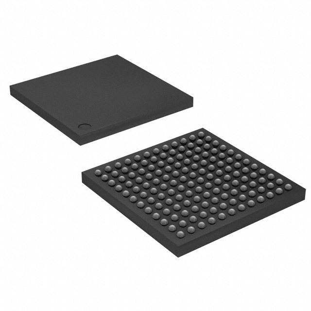
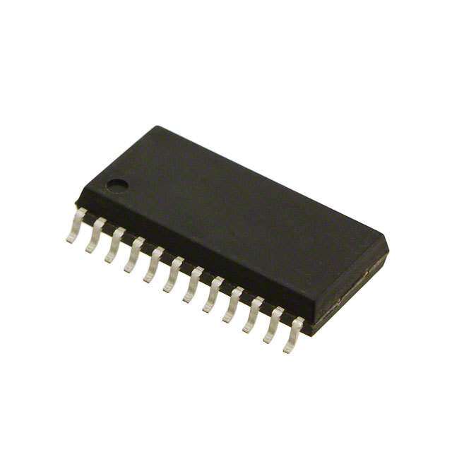
| 产品图片 |
|
| rohs | 符合RoHS无铅 / 符合限制有害物质指令(RoHS)规范要求 |
| 产品系列 | 嵌入式处理器和控制器,微控制器 - MCU,8位微控制器 -MCU,Microchip Technology PIC16F73-I/SPPIC® 16F |
| 数据手册 | 点击此处下载产品Datasheet点击此处下载产品Datasheethttp://www.microchip.com/mymicrochip/filehandler.aspx?ddocname=en012283点击此处下载产品Datasheethttp://www.microchip.com/mymicrochip/filehandler.aspx?ddocname=en531149http://www.microchip.com/mymicrochip/filehandler.aspx?ddocname=en541028http://www.microchip.com/mymicrochip/filehandler.aspx?ddocname=en013772点击此处下载产品Datasheet |
| 产品型号 | PIC16F73-I/SP |
| PCN组件/产地 | http://www.microchip.com/mymicrochip/NotificationDetails.aspx?id=5510&print=viewhttp://www.microchip.com/mymicrochip/NotificationDetails.aspx?id=5577&print=viewhttp://www.microchip.com/mymicrochip/NotificationDetails.aspx?id=5703&print=viewhttp://www.microchip.com/mymicrochip/NotificationDetails.aspx?id=5776&print=view |
| RAM容量 | 192 x 8 |
| 产品培训模块 | http://www.digikey.cn/PTM/IndividualPTM.page?site=cn&lang=zhs&ptm=2046http://www.digikey.cn/PTM/IndividualPTM.page?site=cn&lang=zhs&ptm=25053 |
| 产品目录页面 | |
| 产品种类 | 8位微控制器 -MCU |
| 供应商器件封装 | 28-SPDIP |
| 其它名称 | PIC16F73ISP |
| 包装 | 管件 |
| 可用A/D通道 | 5 |
| 可编程输入/输出端数量 | 22 |
| 商标 | Microchip Technology |
| 处理器系列 | PIC16 |
| 外设 | 欠压检测/复位,POR,PWM,WDT |
| 安装风格 | Through Hole |
| 定时器数量 | 3 Timer |
| 封装 | Tube |
| 封装/外壳 | 28-DIP(0.300",7.62mm) |
| 封装/箱体 | SPDIP-28 |
| 工作温度 | -40°C ~ 85°C |
| 工作电源电压 | 2 V to 5.5 V |
| 工厂包装数量 | 15 |
| 振荡器类型 | 外部 |
| 接口类型 | I2C, SPI, USART |
| 数据RAM大小 | 192 B |
| 数据Ram类型 | RAM |
| 数据ROM大小 | 192 B |
| 数据Rom类型 | Flash |
| 数据总线宽度 | 8 bit |
| 数据转换器 | A/D 5x8b |
| 最大工作温度 | + 85 C |
| 最大时钟频率 | 20 MHz |
| 最小工作温度 | - 40 C |
| 标准包装 | 15 |
| 核心 | PIC |
| 核心处理器 | PIC |
| 核心尺寸 | 8-位 |
| 片上ADC | Yes |
| 电压-电源(Vcc/Vdd) | 4 V ~ 5.5 V |
| 电源电压-最大 | 5.5 V |
| 电源电压-最小 | 4 V |
| 程序存储器大小 | 7 kB |
| 程序存储器类型 | Flash |
| 程序存储容量 | 7KB(4K x 14) |
| 系列 | PIC16 |
| 输入/输出端数量 | 22 I/O |
| 连接性 | I²C, SPI, UART/USART |
| 速度 | 20MHz |


- 商务部:美国ITC正式对集成电路等产品启动337调查
- 曝三星4nm工艺存在良率问题 高通将骁龙8 Gen1或转产台积电
- 太阳诱电将投资9.5亿元在常州建新厂生产MLCC 预计2023年完工
- 英特尔发布欧洲新工厂建设计划 深化IDM 2.0 战略
- 台积电先进制程称霸业界 有大客户加持明年业绩稳了
- 达到5530亿美元!SIA预计今年全球半导体销售额将创下新高
- 英特尔拟将自动驾驶子公司Mobileye上市 估值或超500亿美元
- 三星加码芯片和SET,合并消费电子和移动部门,撤换高东真等 CEO
- 三星电子宣布重大人事变动 还合并消费电子和移动部门
- 海关总署:前11个月进口集成电路产品价值2.52万亿元 增长14.8%


PDF Datasheet 数据手册内容提取
M PIC16F7X Data Sheet 28/40-pin, 8-bit CMOS FLASH Microcontrollers 2002 Microchip Technology Inc. DS30325B
Note the following details of the code protection feature on PICmicro® MCUs. (cid:127) The PICmicro family meets the specifications contained in the Microchip Data Sheet. (cid:127) Microchip believes that its family of PICmicro microcontrollers is one of the most secure products of its kind on the market today, when used in the intended manner and under normal conditions. (cid:127) There are dishonest and possibly illegal methods used to breach the code protection feature. All of these methods, to our knowl- edge, require using the PICmicro microcontroller in a manner outside the operating specifications contained in the data sheet. The person doing so may be engaged in theft of intellectual property. (cid:127) Microchip is willing to work with the customer who is concerned about the integrity of their code. (cid:127) Neither Microchip nor any other semiconductor manufacturer can guarantee the security of their code. Code protection does not mean that we are guaranteeing the product as “unbreakable”. (cid:127) Code protection is constantly evolving. We at Microchip are committed to continuously improving the code protection features of our product. If you have any further questions about this matter, please contact the local sales office nearest to you. Information contained in this publication regarding device Trademarks applications and the like is intended through suggestion only and may be superseded by updates. It is your responsibility to The Microchip name and logo, the Microchip logo, FilterLab, ensure that your application meets with your specifications. KEELOQ, MPLAB, PIC, PICmicro, PICMASTER, PICSTART, No representation or warranty is given and no liability is PRO MATE, SEEVAL and The Embedded Control Solutions assumed by Microchip Technology Incorporated with respect Company are registered trademarks of Microchip Technology to the accuracy or use of such information, or infringement of Incorporated in the U.S.A. and other countries. patents or other intellectual property rights arising from such dsPIC, ECONOMONITOR, FanSense, FlexROM, fuzzyLAB, use or otherwise. Use of Microchip’s products as critical com- In-Circuit Serial Programming, ICSP, ICEPIC, microID, ponents in life support systems is not authorized except with microPort, Migratable Memory, MPASM, MPLIB, MPLINK, express written approval by Microchip. No licenses are con- MPSIM, MXDEV, PICC, PICDEM, PICDEM.net, rfPIC, Select veyed, implicitly or otherwise, under any intellectual property Mode and Total Endurance are trademarks of Microchip rights. Technology Incorporated in the U.S.A. Serialized Quick Term Programming (SQTP) is a service mark of Microchip Technology Incorporated in the U.S.A. All other trademarks mentioned herein are property of their respective companies. © 2002, Microchip Technology Incorporated, Printed in the U.S.A., All Rights Reserved. Printed on recycled paper. Microchip received QS-9000 quality system certification for its worldwide headquarters, design and wafer fabrication facilities in Chandler and Tempe, Arizona in July 1999. The Company’s quality system processes and procedures are QS-9000 compliant for its PICmicro® 8-bit MCUs, KEELOQ® code hopping devices, Serial EEPROMs and microperipheral products. In addition, Microchip’s quality system for the design and manufacture of development systems is ISO 9001 certified. DS30325B - page ii 2002 Microchip Technology Inc.
M PIC16F7X 28/40-Pin 8-Bit CMOS FLASH Microcontrollers Devices Included in this Data Sheet: Peripheral Features: (cid:127) PIC16F73 (cid:127) PIC16F76 (cid:127) Timer0: 8-bit timer/counter with 8-bit prescaler (cid:127) PIC16F74 (cid:127) PIC16F77 (cid:127) Timer1: 16-bit timer/counter with prescaler, can be incremented during SLEEP via external High Performance RISC CPU: crystal/clock (cid:127) Timer2: 8-bit timer/counter with 8-bit period (cid:127) High performance RISC CPU register, prescaler and postscaler (cid:127) Only 35 single word instructions to learn (cid:127) Two Capture, Compare, PWM modules (cid:127) All single cycle instructions except for program - Capture is 16-bit, max. resolution is 12.5 ns branches which are two-cycle - Compare is 16-bit, max. resolution is 200 ns (cid:127) Operating speed: DC - 20 MHz clock input - PWM max. resolution is 10-bit DC - 200 ns instruction cycle (cid:127) 8-bit, up to 8-channel Analog-to-Digital converter (cid:127) Up to 8K x 14 words of FLASH Program Memory, (cid:127) Synchronous Serial Port (SSP) with SPI (Master Up to 368 x 8 bytes of Data Memory (RAM) mode) and I2C (Slave) (cid:127) Pinout compatible to the PIC16C73B/74B/76/77 (cid:127) Universal Synchronous Asynchronous Receiver (cid:127) Pinout compatible to the PIC16F873/874/876/877 Transmitter (USART/SCI) (cid:127) Interrupt capability (up to 12 sources) (cid:127) Parallel Slave Port (PSP), 8-bits wide with (cid:127) Eight level deep hardware stack external RD, WR and CS controls (40/44-pin only) (cid:127) Direct, Indirect and Relative Addressing modes (cid:127) Brown-out detection circuitry for (cid:127) Processor read access to program memory Brown-out Reset (BOR) Special Microcontroller Features: CMOS Technology: (cid:127) Power-on Reset (POR) (cid:127) Low power, high speed CMOS FLASH technology (cid:127) Power-up Timer (PWRT) and (cid:127) Fully static design Oscillator Start-up Timer (OST) (cid:127) Wide operating voltage range: 2.0V to 5.5V (cid:127) Watchdog Timer (WDT) with its own on-chip RC (cid:127) High Sink/Source Current: 25 mA oscillator for reliable operation (cid:127) Industrial temperature range (cid:127) Programmable code protection (cid:127) Low power consumption: (cid:127) Power saving SLEEP mode - < 2 mA typical @ 5V, 4 MHz (cid:127) Selectable oscillator options - 20 µA typical @ 3V, 32 kHz (cid:127) In-Circuit Serial Programming (ICSP) via two - < 1 µA typical standby current pins SSP Program Memory Data 8-bit CCP Timers Device (# Single Word SRAM I/O Interrupts A/D (ch) (PWM) SPI I2C USART 8/16-bit Instructions) (Bytes) (Master) (Slave) PIC16F73 4096 192 22 11 5 2 Yes Yes Yes 2 / 1 PIC16F74 4096 192 33 12 8 2 Yes Yes Yes 2 / 1 PIC16F76 8192 368 22 11 5 2 Yes Yes Yes 2 / 1 PIC16F77 8192 368 33 12 8 2 Yes Yes Yes 2 / 1 2002 Microchip Technology Inc. DS30325B-page 1
PIC16F7X Pin Diagrams DIP, SOIC, SSOP MCLR/VPP 1 28 RB7/PGD RA0/AN0 2 27 RB6/PGC RA1/AN1 3 26 RB5 RA2/AN2 4 25 RB4 RA3/AN3/VREF 5 73 24 RB3/PGM RA4/T0CKI 6 6/ 23 RB2 RA5/AN4/SS 7 7 22 RB1 F VSS 8 6 21 RB0/INT OSC1/CLKIN 9 C1 20 VDD OSC2/CLKOUT 10 PI 19 VSS RC0/T1OSO/T1CKI 11 18 RC7/RX/DT RC1/T1OSI/CCP2 12 17 RC6/TX/CK RC2/CCP1 13 16 RC5/SDO RC3/SCK/SCL 14 15 RC4/SDI/SDA MLF N1N0VPPGDGC AAR/PP A1/A0/CLB7/B6/B5B4 RRMRRRR 28272625242322 RA2/AN2 1 21 RB3/PGM RA3/AN3/VREF 2 20 RB2 RA4/T0CKI 3 PIC16F73 19 RB1 RA5/AN4/SS 4 18 RB0/INT PIC16F76 VSS 5 17 VDD OSC1/CLKI 6 16 VSS OSC2/CLKO 7 15 RC7/RX/DT 8 91011121314 PDIP 0/T1OSO/T1CKIC1/T1OSI/CCP2RC2/CCP1RC3/SCK/SCLRC4/SDI/SDARC5/SDORC6/TX/CK CR R MCLR/VPP 1 40 RB7/PGD RA0/AN0 2 39 RB6/PGC RA1/AN1 3 38 RB5 RA2/AN2 4 37 RB4 RA3/AN3/VREF 5 36 RB3/PGM RA4/T0CKI 6 35 RB2 RA5/AN4/SS 7 34 RB1 4 RE0/RD/AN5 8 7 33 RB0/INT RE1/WR/AN6 9 77/ 32 VDD RE2/CS/AN7 10 F 31 VSS 6 VDD 11 1 30 RD7/PSP7 OSC1/CLVKSINS 1123 PIC 2298 RRDD65//PPSSPP65 OSC2/CLKOUT 14 27 RD4/PSP4 RC0/T1OSO/T1CKI 15 26 RC7/RX/DT RC1/T1OSI/CCP2 16 25 RC6/TX/CK RC2/CCP1 17 24 RC5/SDO RC3/SCK/SCL 18 23 RC4/SDI/SDA RD0/PSP0 19 22 RD3/PSP3 RD1/PSP1 20 21 RD2/PSP2 DS30325B-page 2 2002 Microchip Technology Inc.
PIC16F7X Pin Diagrams (Continued) PLCC F E R N3/VN2N1N0VPP GDGC AAAAR/ PP A3/A2/A1/A0/CLCB7/B6/B5B4C RRRRMNRRRRN 65432143210 RA4/T0CKI 7 4444439 RB3/PGM RA5/AN4/SS 8 38 RB2 RE0/RD/AN5 9 37 RB1 RREE12//WCRS//AANN67 1110 PIC16F77 3356 RVDBD0/INT VDD 12 PIC16F74 34 VSS VSS 13 33 RD7/PSP7 OSC1/CLKIN 14 32 RD6/PSP6 OSC2/CLKOUT 15 31 RD5/PSP5 RC0/T1OSO/T1CK1 16 30 RD4/PSP4 NC 17 29 RC7/RX/DT 89012345678 11222222222 21L0123AOKC PPCPPPPDDCN 1/T1OSI/CCRC2/CCRC3/SCK/SRD0/PSRD1/PSRD2/PSRD3/PSRC4/SDI/SRC5/SRC6/TX/ C R QFP 2 P X/CKDODI/SDASP3SP2SP1SP0CK/SCLCP11OSI/CC TSSPPPPSCT 6/5/4/3/2/1/0/3/2/1/ CCCDDDDCCCC RRRRRRRRRRN 43210987654 44444333333 RC7/RX/DT 1 33 NC RD4/PSP4 2 32 RC0/T1OSO/T1CKI RD5/PSP5 3 31 OSC2/CLKOUT RD6/PSP6 4 30 OSC1/CLKIN RD7/PSP7 5 PIC16F77 29 VSS VSS 6 PIC16F74 28 VDD VDD 7 27 RE2/AN7/CS RB0/INT 8 26 RE1/AN6/WR RB1 9 25 RE0/AN5/RD RB2 10 24 RA5/AN4/SS RB3/PGM 11 23 RA4/T0CKI 23456789012 11111111222 CC45CDP012F NNRBRBRB6/PGRB7/PGMCLR/VPRA0/ANRA1/ANRA2/ANAN3/VRE 3/ A R 2002 Microchip Technology Inc. DS30325B-page 3
PIC16F7X Table of Contents 1.0 Device Overview......................................................................................................................................................................... 5 2.0 Memory Organization................................................................................................................................................................ 13 3.0 Reading Program Memory........................................................................................................................................................ 29 4.0 I/O Ports.................................................................................................................................................................................... 31 5.0 Timer0 Module.......................................................................................................................................................................... 43 6.0 Timer1 Module.......................................................................................................................................................................... 47 7.0 Timer2 Module.......................................................................................................................................................................... 51 8.0 Capture/Compare/PWM Modules............................................................................................................................................. 53 9.0 Synchronous Serial Port (SSP) Module.................................................................................................................................... 59 10.0 Universal Synchronous Asynchronous Receiver Transmitter (USART)................................................................................... 69 11.0 Analog-to-Digital Converter (A/D) Module................................................................................................................................ 83 12.0 Special Features of the CPU.................................................................................................................................................... 89 13.0 Instruction Set Summary......................................................................................................................................................... 105 14.0 Development Support............................................................................................................................................................. 113 15.0 Electrical Characteristics......................................................................................................................................................... 119 16.0 DC and AC Characteristics Graphs and Tables..................................................................................................................... 141 17.0 Packaging Information............................................................................................................................................................ 151 Appendix A: Revision History ........................................................................................................................................................ 161 Appendix B: Device Differences.................................................................................................................................................... 161 Appendix C: Conversion Considerations....................................................................................................................................... 162 Index................................................................................................................................................................................................. 163 On-Line Support................................................................................................................................................................................ 169 Reader Response............................................................................................................................................................................. 170 PIC16F7X Product Identification System.......................................................................................................................................... 171 TO OUR VALUED CUSTOMERS It is our intention to provide our valued customers with the best documentation possible to ensure successful use of your Microchip products. To this end, we will continue to improve our publications to better suit your needs. Our publications will be refined and enhanced as new volumes and updates are introduced. If you have any questions or comments regarding this publication, please contact the Marketing Communications Department via E-mail at docerrors@mail.microchip.com or fax the Reader Response Form in the back of this data sheet to (480) 792-4150. We welcome your feedback. Most Current Data Sheet To obtain the most up-to-date version of this data sheet, please register at our Worldwide Web site at: http://www.microchip.com You can determine the version of a data sheet by examining its literature number found on the bottom outside corner of any page. The last character of the literature number is the version number, (e.g., DS30000A is version A of document DS30000). Errata An errata sheet, describing minor operational differences from the data sheet and recommended workarounds, may exist for current devices. As device/documentation issues become known to us, we will publish an errata sheet. The errata will specify the revision of silicon and revision of document to which it applies. To determine if an errata sheet exists for a particular device, please check with one of the following: (cid:127) Microchip’s Worldwide Web site; http://www.microchip.com (cid:127) Your local Microchip sales office (see last page) (cid:127) The Microchip Corporate Literature Center; U.S. FAX: (480) 792-7277 When contacting a sales office or the literature center, please specify which device, revision of silicon and data sheet (include liter- ature number) you are using. Customer Notification System Register on our web site at www.microchip.com/cn to receive the most current information on all of our products. DS30325B-page 4 2002 Microchip Technology Inc.
PIC16F7X 1.0 DEVICE OVERVIEW The available features are summarized in Table1-1. Block diagrams of the PIC16F73/76 and PIC16F74/77 This document contains device specific information devices are provided in Figure1-1 and Figure1-2, about the following devices: respectively. The pinouts for these device families are (cid:127) PIC16F73 listed in Table1-2 and Table1-3. (cid:127) PIC16F74 Additional information may be found in the PICmicro™ (cid:127) PIC16F76 Mid-Range Reference Manual (DS33023), which may be obtained from your local Microchip Sales Represen- (cid:127) PIC16F77 tative or downloaded from the Microchip website. The PIC16F73/76 devices are available only in 28-pin pack- Reference Manual should be considered a complemen- ages, while PIC16F74/77 devices are available in tary document to this data sheet, and is highly recom- 40-pin and 44-pin packages. All devices in the mended reading for a better understanding of the device PIC16F7X family share common architecture, with the architecture and operation of the peripheral modules. following differences: (cid:127) The PIC16F73 and PIC16F76 have one-half of the total on-chip memory of the PIC16F74 and PIC16F77 (cid:127) The 28-pin devices have 3 I/O ports, while the 40/44-pin devices have 5 (cid:127) The 28-pin devices have 11 interrupts, while the 40/44-pin devices have 12 (cid:127) The 28-pin devices have 5 A/D input channels, while the 40/44-pin devices have 8 (cid:127) The Parallel Slave Port is implemented only on the 40/44-pin devices TABLE 1-1: PIC16F7X DEVICE FEATURES Key Features PIC16F73 PIC16F74 PIC16F76 PIC16F77 Operating Frequency DC - 20 MHz DC - 20 MHz DC - 20 MHz DC - 20 MHz RESETS (and Delays) POR, BOR POR, BOR POR, BOR POR, BOR (PWRT, OST) (PWRT, OST) (PWRT, OST) (PWRT, OST) FLASH Program Memory 4K 4K 8K 8K (14-bit words) Data Memory (bytes) 192 192 368 368 Interrupts 11 12 11 12 I/O Ports Ports A,B,C Ports A,B,C,D,E Ports A,B,C Ports A,B,C,D,E Timers 3 3 3 3 Capture/Compare/PWM Modules 2 2 2 2 Serial Communications SSP, USART SSP, USART SSP, USART SSP, USART Parallel Communications — PSP — PSP 8-bit Analog-to-Digital Module 5 Input Channels 8 Input Channels 5 Input Channels 8 Input Channels Instruction Set 35 Instructions 35 Instructions 35 Instructions 35 Instructions Packaging 28-pin DIP 40-pin PDIP 28-pin DIP 40-pin PDIP 28-pin SOIC 44-pin PLCC 28-pin SOIC 44-pin PLCC 28-pin SSOP 44-pin TQFP 28-pin SSOP 44-pin TQFP 28-pin MLF 28-pin MLF 2002 Microchip Technology Inc. DS30325B-page 5
PIC16F7X FIGURE 1-1: PIC16F73 AND PIC16F76 BLOCK DIAGRAM 13 Data Bus 8 PORTA Program Counter FLASH RA0/AN0 Program RA1/AN1 Memory RAM RA2/AN2/ 8 Level Stack File RA3/AN3/VREF (13-bit) Registers RA4/T0CKI RA5/AN4/SS Program Bus 14 RAM Addr(1) 9 PORTB Addr MUX RB0/INT Instruction reg RB1 Direct Addr 7 Indirect RB2 8 Addr RB3/PGM RB4 FSR reg RB5 RB6/PGC STATUS reg RB7/PGD 8 PORTC RC0/T1OSO/T1CKI Power-up 3 MUX RC1/T1OSI/CCP2 Timer RC2/CCP1 RC3/SCK/SCL Instruction Oscillator RC4/SDI/SDA DCecoondtreo l& Start-up Timer ALU RC5/SDO Power-on RC6/TX/CK Reset 8 RC7/RX/DT Timing Watchdog Generation Timer W reg OSC1/CLKIN Brown-out OSC2/CLKOUT Reset MCLR VDD, VSS Timer0 Timer1 Timer2 8-bit A/D Synchronous CCP1 CCP2 USART Serial Port Device Program FLASH Data Memory PIC16F73 4K 192 Bytes PIC16F76 8K 368 Bytes Note1:Higher order bits are from the STATUS register. DS30325B-page 6 2002 Microchip Technology Inc.
PIC16F7X FIGURE 1-2: PIC16F74 AND PIC16F77 BLOCK DIAGRAM 13 Data Bus 8 PORTA Program Counter FLASH RA0/AN0 Program RA1/AN1 Memory RAM RA2/AN2 8 Level Stack RA3/AN3/VREF File (13-bit) Registers RA4/T0CKI RA5/AN4/SS Program Bus 14 RAM Addr(1) 9 PORTB RB0/INT Addr MUX RB1 Instruction reg RB2 Direct Addr 7 Indirect RB3/PGM 8 Addr RB4 FSR reg RB5 RB6/PGC STATUS reg RB7/PGD 8 PORTC RC0/T1OSO/T1CKI RC1/T1OSI/CCP2 Power-up 3 MUX RC2/CCP1 Timer RC3/SCK/SCL RC4/SDI/SDA Instruction Oscillator DCecoondtreo l& Start-up Timer ALU RRCC56//STXD/OCK Power-on Reset 8 RC7/RX/DT Timing Watchdog PORTD Generation Timer W reg RD0/PSP0 OSC1/CLKIN Brown-out RD1/PSP1 OSC2/CLKOUT Reset RD2/PSP2 RD3/PSP3 RD4/PSP4 RD5/PSP5 RD6/PSP6 RD7/PSP7 MCLR VDD, VSS PORTE RE0/AN5/RD RE1/AN6/WR RE2/AN7/CS Timer0 Timer1 Timer2 8-bit A/D Synchronous CCP1 CCP2 USART Parallel Slave Port Serial Port Device Program FLASH Data Memory PIC16F74 4K 192 Bytes PIC16F77 8K 368 Bytes Note1:Higher order bits are from the STATUS register. 2002 Microchip Technology Inc. DS30325B-page 7
PIC16F7X TABLE 1-2: PIC16F73 AND PIC16F76 PINOUT DESCRIPTION DIP SSOP MLF I/O/P Buffer Pin Name Description SOIC Pin# Type Type Pin# OSC1/CLKI 9 6 ST/CMOS(3) Oscillator crystal or external clock input. OSC1 I Oscillator crystal input or external clock source input. ST buffer when configured in RC mode. Otherwise CMOS. CLKI I External clock source input. Always associated with pin function OSC1 (see OSC1/CLKI, OSC2/CLKO pins). OSC2/CLKO 10 7 — Oscillator crystal or clock output. OSC2 O Oscillator crystal output. Connects to crystal or resonator in Crystal Oscillator mode. CLKO O In RC mode, OSC2 pin outputs CLKO, which has 1/4 the frequency of OSC1 and denotes the instruction cycle rate. MCLR/VPP 1 26 ST Master Clear (input) or programming voltage (output). MCLR I Master Clear (Reset) input. This pin is an active low RESET to the device. VPP P Programming voltage input. PORTA is a bi-directional I/O port. RA0/AN0 2 27 TTL RA0 I/O Digital I/O. AN0 I Analog input 0. RA1/AN1 3 28 TTL RA1 I/O Digital I/O. AN1 I Analog input 1. RA2/AN2 4 1 TTL RA2 I/O Digital I/O. AN2 I Analog input 2. RA3/AN3/VREF 5 2 TTL RA3 I/O Digital I/O. AN3 I Analog input 3. VREF I A/D reference voltage input. RA4/T0CKI 6 4 ST RA4 I/O Digital I/O – Open drain when configured as output. T0CKI I Timer0 external clock input. RA5/SS/AN4 7 5 TTL RA5 I/O Digital I/O. SS I SPI slave select input. AN4 I Analog input 4. Legend: I = input O = output I/O = input/output P = power — = Not used TTL = TTL input ST = Schmitt Trigger input Note 1: This buffer is a Schmitt Trigger input when configured as the external interrupt. 2: This buffer is a Schmitt Trigger input when used in Serial Programming mode. 3: This buffer is a Schmitt Trigger input when configured in RC Oscillator mode and a CMOS input otherwise. DS30325B-page 8 2002 Microchip Technology Inc.
PIC16F7X TABLE 1-2: PIC16F73 AND PIC16F76 PINOUT DESCRIPTION (CONTINUED) DIP SSOP MLF I/O/P Buffer Pin Name Description SOIC Pin# Type Type Pin# PORTB is a bi-directional I/O port. PORTB can be software programmed for internal weak pull-up on all inputs. RB0/INT 21 18 TTL/ST(1) RB0 I/O Digital I/O. INT I External interrupt. RB1 22 19 I/O TTL Digital I/O. RB2 23 20 I/O TTL Digital I/O. RB3/PGM 24 21 TTL RB3 I/O Digital I/O. PGM I/O Low voltage ICSP programming enable pin. RB4 25 22 I/O TTL Digital I/O. RB5 26 23 I/O TTL Digital I/O. RB6/PGC 27 24 TTL/ST(2) RB6 I/O Digital I/O. PGC I/O In-Circuit Debugger and ICSP programming clock. RB7/PGD 28 25 TTL/ST(2) RB7 I/O Digital I/O. PGD I/O In-Circuit Debugger and ICSP programming data. PORTC is a bi-directional I/O port. RC0/T1OSO/T1CKI 11 8 ST RC0 I/O Digital I/O. T1OSO O Timer1 oscillator output. T1CKI I Timer1 external clock input. RC1/T1OSI/CCP2 12 9 ST RC1 I/O Digital I/O. T1OSI I Timer1 oscillator input. CCP2 I/O Capture2 input, Compare2 output, PWM2 output. RC2/CCP1 13 10 ST RC2 I/O Digital I/O. CCP1 I/O Capture1 input/Compare1 output/PWM1 output. RC3/SCK/SCL 14 11 ST RC3 I/O Digital I/O. SCK I/O Synchronous serial clock input/output for SPI mode. SCL I/O Synchronous serial clock input/output for I2C mode. RC4/SDI/SDA 15 12 ST RC4 I/O Digital I/O. SDI I SPI data in. SDA I/O I2C data I/O. RC5/SDO 16 13 ST RC5 I/O Digital I/O. SDO O SPI data out. RC6/TX/CK 17 14 ST RC6 I/O Digital I/O. TX O USART asynchronous transmit. CK I/O USART 1 synchronous clock. RC7/RX/DT 18 15 ST RC7 I/O Digital I/O. RX I USART asynchronous receive. DT I/O USART synchronous data. VSS 8, 19 5, 16 P — Ground reference for logic and I/O pins. VDD 20 17 P — Positive supply for logic and I/O pins. Legend: I = input O = output I/O = input/output P = power — = Not used TTL = TTL input ST = Schmitt Trigger input Note 1: This buffer is a Schmitt Trigger input when configured as the external interrupt. 2: This buffer is a Schmitt Trigger input when used in Serial Programming mode. 3: This buffer is a Schmitt Trigger input when configured in RC Oscillator mode and a CMOS input otherwise. 2002 Microchip Technology Inc. DS30325B-page 9
PIC16F7X TABLE 1-3: PIC16F74 AND PIC16F77 PINOUT DESCRIPTION DIP PLCC QFP I/O/P Buffer Pin Name Description Pin# Pin# Pin# Type Type OSC1/CLKI 13 14 30 ST/CMOS(4) Oscillator crystal or external clock input. OSC1 I Oscillator crystal input or external clock source input. ST buffer when configured in RC mode. Otherwise CLKI I CMOS. External clock source input. Always associated with pin function OSC1 (see OSC1/CLKI, OSC2/CLKO pins). OSC2/CLKO 14 15 31 — Oscillator crystal or clock output. OSC2 O Oscillator crystal output. Connects to crystal or resonator in Crystal Oscillator mode. CLKO O In RC mode, OSC2 pin outputs CLKO, which has 1/4 the frequency of OSC1 and denotes the instruction cycle rate. MCLR/VPP 1 2 18 ST Master Clear (input) or programming voltage (output). MCLR I Master Clear (Reset) input. This pin is an active low RESET to the device. VPP P Programming voltage input. PORTA is a bi-directional I/O port. RA0/AN0 2 3 19 TTL RA0 I/O Digital I/O. AN0 I Analog input 0. RA1/AN1 3 4 20 TTL RA1 I/O Digital I/O. AN1 I Analog input 1. RA2/AN2 4 5 21 TTL RA2 I/O Digital I/O. AN2 I Analog input 2. RA3/AN3/VREF 5 6 22 TTL RA3 I/O Digital I/O. AN3 I Analog input 3. VREF I A/D reference voltage input. RA4/T0CKI 6 7 23 ST RA4 I/O Digital I/O – Open drain when configured as output. T0CKI I Timer0 external clock input. RA5/SS/AN4 7 8 24 TTL RA5 I/O Digital I/O. SS I SPI slave select input. AN4 I Analog input 4. Legend: I = input O = output I/O = input/output P = power — = Not used TTL = TTL input ST = Schmitt Trigger input Note 1: This buffer is a Schmitt Trigger input when configured as an external interrupt. 2: This buffer is a Schmitt Trigger input when used in Serial Programming mode. 3: This buffer is a Schmitt Trigger input when configured as general purpose I/O and a TTL input when used in the Parallel Slave Port mode (for interfacing to a microprocessor bus). 4: This buffer is a Schmitt Trigger input when configured in RC Oscillator mode and a CMOS input otherwise. DS30325B-page 10 2002 Microchip Technology Inc.
PIC16F7X TABLE 1-3: PIC16F74 AND PIC16F77 PINOUT DESCRIPTION (CONTINUED) DIP PLCC QFP I/O/P Buffer Pin Name Description Pin# Pin# Pin# Type Type PORTB is a bi-directional I/O port. PORTB can be software programmed for internal weak pull-up on all inputs. RB0/INT 33 36 8 TTL/ST(1) RB0 I/O Digital I/O. INT I External interrupt. RB1 34 37 9 I/O TTL Digital I/O. RB2 35 38 10 I/O TTL Digital I/O. RB3/PGM 36 39 11 TTL RB3 I/O Digital I/O. PGM I/O Low voltage ICSP programming enable pin. RB4 37 41 14 I/O TTL Digital I/O. RB5 38 42 15 I/O TTL Digital I/O. RB6/PGC 39 43 16 TTL/ST(2) RB6 I/O Digital I/O. PGC I/O In-Circuit Debugger and ICSP programming clock. RB7/PGD 40 44 17 TTL/ST(2) RB7 I/O Digital I/O. PGD I/O In-Circuit Debugger and ICSP programming data. PORTC is a bi-directional I/O port. RC0/T1OSO/T1CKI 15 16 32 ST RC0 I/O Digital I/O. T1OSO O Timer1 oscillator output. T1CKI I Timer1 external clock input. RC1/T1OSI/CCP2 16 18 35 ST RC1 I/O Digital I/O. T1OSI I Timer1 oscillator input. CCP2 I/O Capture2 input, Compare2 output, PWM2 output. RC2/CCP1 17 19 36 ST RC2 I/O Digital I/O. CCP1 I/O Capture1 input/Compare1 output/PWM1 output RC3/SCK/SCL 18 20 37 ST RC3 I/O Digital I/O SCK I/O Synchronous serial clock input/output for SPI mode. SCL I/O Synchronous serial clock input/output for I2C mode. RC4/SDI/SDA 23 25 42 ST RC4 I/O Digital I/O. SDI I SPI data in. SDA I/O I2C data I/O. RC5/SDO 24 26 43 ST RC5 I/O Digital I/O. SDO O SPI data out. RC6/TX/CK 25 27 44 ST RC6 I/O Digital I/O. TX O USART asynchronous transmit. CK I/O USART 1 synchronous clock. RC7/RX/DT 26 29 1 ST RC7 I/O Digital I/O. RX I USART asynchronous receive. DT I/O USART synchronous data. Legend: I = input O = output I/O = input/output P = power — = Not used TTL = TTL input ST = Schmitt Trigger input Note 1: This buffer is a Schmitt Trigger input when configured as an external interrupt. 2: This buffer is a Schmitt Trigger input when used in Serial Programming mode. 3: This buffer is a Schmitt Trigger input when configured as general purpose I/O and a TTL input when used in the Parallel Slave Port mode (for interfacing to a microprocessor bus). 4: This buffer is a Schmitt Trigger input when configured in RC Oscillator mode and a CMOS input otherwise. 2002 Microchip Technology Inc. DS30325B-page 11
PIC16F7X TABLE 1-3: PIC16F74 AND PIC16F77 PINOUT DESCRIPTION (CONTINUED) DIP PLCC QFP I/O/P Buffer Pin Name Description Pin# Pin# Pin# Type Type PORTD is a bi-directional I/O port or parallel slave port when interfacing to a microprocessor bus. RD0/PSP0 19 21 38 ST/TTL(3) RD0 I/O Digital I/O. PSP0 I/O Parallel Slave Port data. RD1/PSP1 20 22 39 I ST/TTL(3) RD1 I/O Digital I/O. PSP1 I/O Parallel Slave Port data. RD2/PSP2 21 23 40 I ST/TTL(3) RD2 I/O Digital I/O. PSP2 I/O Parallel Slave Port data. RD3/PSP3 22 24 41 ST/TTL(3) RD3 I/O Digital I/O. PSP3 I/O Parallel Slave Port data. RD4/PSP4 27 30 2 ST/TTL(3) RD4 I/O Digital I/O. PSP4 I/O Parallel Slave Port data. RD5/PSP5 28 31 3 ST/TTL(3) RD5 I/O Digital I/O. PSP5 I/O Parallel Slave Port data. RD6/PSP6 29 32 4 ST/TTL(3) RD6 I/O Digital I/O. PSP6 I/O Parallel Slave Port data. RD7/PSP7 30 33 5 ST/TTL(3) RD7 I/O Digital I/O. PSP7 I/O Parallel Slave Port data. PORTE is a bi-directional I/O port. RE0/RD/AN5 8 9 25 ST/TTL(3) RE0 I/O Digital I/O. RD I Read control for parallel slave port . AN5 I Analog input 5. RE1/WR/AN6 9 10 26 ST/TTL(3) RE1 I/O Digital I/O. WR I Write control for parallel slave port . AN6 I Analog input 6. RE2/CS/AN7 10 11 27 ST/TTL(3) RE2 I/O Digital I/O. CS I Chip select control for parallel slave port . AN7 I Analog input 7. VSS 12,31 13,34 6,29 P — Ground reference for logic and I/O pins. VDD 11,32 12,35 7,28 P — Positive supply for logic and I/O pins. NC — 1,17,2 12,13, — These pins are not internally connected. These pins should 8, 40 33, 34 be left unconnected. Legend: I = input O = output I/O = input/output P = power — = Not used TTL = TTL input ST = Schmitt Trigger input Note 1: This buffer is a Schmitt Trigger input when configured as an external interrupt. 2: This buffer is a Schmitt Trigger input when used in Serial Programming mode. 3: This buffer is a Schmitt Trigger input when configured as general purpose I/O and a TTL input when used in the Parallel Slave Port mode (for interfacing to a microprocessor bus). 4: This buffer is a Schmitt Trigger input when configured in RC Oscillator mode and a CMOS input otherwise. DS30325B-page 12 2002 Microchip Technology Inc.
PIC16F7X 2.0 MEMORY ORGANIZATION 2.2 Data Memory Organization There are two memory blocks in each of these The Data Memory is partitioned into multiple banks, PICmicro® MCUs. The Program Memory and Data which contain the General Purpose Registers and the Memory have separate buses so that concurrent Special Function Registers. Bits RP1 (STATUS<6>) access can occur and is detailed in this section. The and RP0 (STATUS<5>) are the bank select bits: Program Memory can be read internally by user code RP1:RP0 Bank (see Section3.0). 00 0 Additional information on device memory may be found in the PICmicro Mid-Range Reference Manual 01 1 (DS33023). 10 2 11 3 2.1 Program Memory Organization Each bank extends up to 7Fh (128 bytes). The lower The PIC16F7X devices have a 13-bit program counter locations of each bank are reserved for the Special capable of addressing an 8K word x 14-bit program Function Registers. Above the Special Function Regis- memory space. The PIC16F77/76 devices have ters are General Purpose Registers, implemented as 8Kwords of FLASH program memory and the static RAM. All implemented banks contain Special PIC16F73/74 devices have 4K words. The program Function Registers. Some frequently used Special memory maps for PIC16F7X devices are shown in Function Registers from one bank may be mirrored in Figure2-1. Accessing a location above the physically another bank for code reduction and quicker access. implemented address will cause a wraparound. The RESET Vector is at 0000h and the Interrupt Vector 2.2.1 GENERAL PURPOSE REGISTER is at 0004h. FILE The register file (shown in Figure2-2 and Figure2-3) can be accessed either directly, or indirectly, through the File Select Register FSR. FIGURE 2-1: PROGRAM MEMORY MAPS AND STACKS FOR PIC16F7X DEVICES PIC16F76/77 PIC16F73/74 PC<12:0> PC<12:0> CALL, RETURN 13 CALL, RETURN 13 RETFIE, RETLW RETFIE, RETLW Stack Level 1 Stack Level 1 Stack Level 2 Stack Level 2 Stack Level 8 Stack Level 8 RESET Vector 0000h RESET Vector 0000h Interrupt Vector 0004h Interrupt Vector 0004h 0005h 0005h Page 0 Page 0 On-Chip 07FFh 07FFh Program 0800h 0800h Memory Page 1 Page 1 On-Chip 0FFFh 0FFFh Program 1000h 1000h Memory Page 2 17FFh Unimplemented 1800h Read as ‘0’ Page 3 1FFFh 1FFFh 2002 Microchip Technology Inc. DS30325B-page 13
PIC16F7X FIGURE 2-2: PIC16F77/76 REGISTER FILE MAP File File File File Address Address Address Address Indirect addr.(*) 00h Indirect addr.(*) 80h Indirect addr.(*) 100h Indirect addr.(*) 180h TMR0 01h OPTION_REG 81h TMR0 101h OPTION_REG 181h PCL 02h PCL 82h PCL 102h PCL 182h STATUS 03h STATUS 83h STATUS 103h STATUS 183h FSR 04h FSR 84h FSR 104h FSR 184h PORTA 05h TRISA 85h 105h 185h PORTB 06h TRISB 86h PORTB 106h TRISB 186h PORTC 07h TRISC 87h 107h 187h PORTD(1) 08h TRISD(1) 88h 108h 188h PORTE(1) 09h TRISE(1) 89h 109h 189h PCLATH 0Ah PCLATH 8Ah PCLATH 10Ah PCLATH 18Ah INTCON 0Bh INTCON 8Bh INTCON 10Bh INTCON 18Bh PIR1 0Ch PIE1 8Ch PMDATA 10Ch PMCON1 18Ch PIR2 0Dh PIE2 8Dh PMADR 10Dh 18Dh TMR1L 0Eh PCON 8Eh PMDATH 10Eh 18Eh TMR1H 0Fh 8Fh PMADRH 10Fh 18Fh T1CON 10h 90h 110h 190h TMR2 11h 91h 111h 191h T2CON 12h PR2 92h 112h 192h SSPBUF 13h SSPADD 93h 113h 193h SSPCON 14h SSPSTAT 94h 114h 194h CCPR1L 15h 95h 115h 195h CCPR1H 16h 96h 116h 196h CCP1CON 17h 97h General 117h General 197h Purpose Purpose RCSTA 18h TXSTA 98h Register 118h Register 198h TXREG 19h SPBRG 99h 16 Bytes 119h 16 Bytes 199h RCREG 1Ah 9Ah 11Ah 19Ah CCPR2L 1Bh 9Bh 11Bh 19Bh CCPR2H 1Ch 9Ch 11Ch 19Ch CCP2CON 1Dh 9Dh 11Dh 19Dh ADRES 1Eh 9Eh 11Eh 19Eh ADCON0 1Fh ADCON1 9Fh 11Fh 19Fh 20h A0h 120h 1A0h General General General General Purpose Purpose Purpose Purpose Register Register Register Register 80 Bytes 80 Bytes 80 Bytes 96 Bytes EFh 16Fh 1EFh accesses F0h accesses 170h accesses 1F0h 70h-7Fh 70h-7Fh 70h - 7Fh 7Fh FFh 17Fh 1FFh Bank 0 Bank 1 Bank 2 Bank 3 Unimplemented data memory locations, read as ’0’. * Not a physical register. Note 1: These registers are not implemented on 28-pin devices. DS30325B-page 14 2002 Microchip Technology Inc.
PIC16F7X FIGURE 2-3: PIC16F74/73 REGISTER FILE MAP File File File File Address Address Address Address Indirect addr.(*) 00h Indirect addr.(*) 80h Indirect addr.(*) 100h Indirect addr.(*) 180h TMR0 01h OPTION_REG 81h TMR0 101h OPTION_REG 181h PCL 02h PCL 82h PCL 102h PCL 182h STATUS 03h STATUS 83h STATUS 103h STATUS 183h FSR 04h FSR 84h FSR 104h FSR 184h PORTA 05h TRISA 85h 105h 185h PORTB 06h TRISB 86h PORTB 106h TRISB 186h PORTC 07h TRISC 87h 107h 187h PORTD(1) 08h TRISD(1) 88h 108h 188h PORTE(1) 09h TRISE(1) 89h 109h 189h PCLATH 0Ah PCLATH 8Ah PCLATH 10Ah PCLATH 18Ah INTCON 0Bh INTCON 8Bh INTCON 10Bh INTCON 18Bh PIR1 0Ch PIE1 8Ch PMDATA 10Ch PMCON1 18Ch PIR2 0Dh PIE2 8Dh PMADR 10Dh 18Dh TMR1L 0Eh PCON 8Eh PMDATH 10Eh 18Eh TMR1H 0Fh 8Fh PMADRH 10Fh 18Fh T1CON 10h 90h 110h 190h TMR2 11h 91h T2CON 12h PR2 92h SSPBUF 13h SSPADD 93h SSPCON 14h SSPSTAT 94h CCPR1L 15h 95h CCPR1H 16h 96h CCP1CON 17h 97h RCSTA 18h TXSTA 98h TXREG 19h SPBRG 99h RCREG 1Ah 9Ah CCPR2L 1Bh 9Bh CCPR2H 1Ch 9Ch CCP2CON 1Dh 9Dh ADRES 1Eh 9Eh ADCON0 1Fh ADCON1 9Fh 120h 1A0h 20h A0h General General Purpose Purpose accesses accesses Register Register 20h-7Fh A0h - FFh 96 Bytes 96 Bytes 16Fh 1EFh 170h 1F0h 7Fh FFh 17Fh 1FFh Bank 0 Bank 1 Bank 2 Bank 3 Unimplemented data memory locations, read as ’0’. * Not a physical register. Note 1: These registers are not implemented on 28-pin devices. 2002 Microchip Technology Inc. DS30325B-page 15
PIC16F7X 2.2.2 SPECIAL FUNCTION REGISTERS The Special Function Registers can be classified into two sets: core (CPU) and peripheral. Those registers The Special Function Registers are registers used by associated with the core functions are described in the CPU and peripheral modules for controlling the detail in this section. Those related to the operation of desired operation of the device. These registers are the peripheral features are described in detail in the implemented as static RAM. A list of these registers is peripheral feature section. given in Table2-1. TABLE 2-1: SPECIAL FUNCTION REGISTER SUMMARY Value on: Details Address Name Bit 7 Bit 6 Bit 5 Bit 4 Bit 3 Bit 2 Bit 1 Bit 0 POR, on page BOR Bank 0 00h(4) INDF Addressing this location uses contents of FSR to address data memory (not a physical register) 0000 0000 27, 96 01h TMR0 Timer0 Module Register xxxx xxxx 45, 96 02h(4) PCL Program Counter (PC) Least Significant Byte 0000 0000 26, 96 03h(4) STATUS IRP RP1 RP0 TO PD Z DC C 0001 1xxx 19, 96 04h(4) FSR Indirect Data Memory Address Pointer xxxx xxxx 27, 96 05h PORTA — — PORTA Data Latch when written: PORTA pins when read --0x 0000 32, 96 06h PORTB PORTB Data Latch when written: PORTB pins when read xxxx xxxx 34, 96 07h PORTC PORTC Data Latch when written: PORTC pins when read xxxx xxxx 35, 96 08h(5) PORTD PORTD Data Latch when written: PORTD pins when read xxxx xxxx 36, 96 09h(5) PORTE — — — — — RE2 RE1 RE0 ---- -xxx 39, 96 0Ah(1,4) PCLATH — — — Write Buffer for the upper 5 bits of the Program Counter ---0 0000 26, 96 0Bh(4) INTCON GIE PEIE TMR0IE INTE RBIE TMR0IF INTF RBIF 0000 000x 21, 96 0Ch PIR1 PSPIF(3) ADIF RCIF TXIF SSPIF CCP1IF TMR2IF TMR1IF 0000 0000 23, 96 0Dh PIR2 — — — — — — — CCP2IF ---- ---0 24, 96 0Eh TMR1L Holding Register for the Least Significant Byte of the 16-bit TMR1 Register xxxx xxxx 50, 96 0Fh TMR1H Holding Register for the Most Significant Byte of the 16-bit TMR1 Register xxxx xxxx 50, 96 10h T1CON — — T1CKPS1 T1CKPS0 T1OSCEN T1SYNC TMR1CS TMR1ON --00 0000 47, 96 11h TMR2 Timer2 Module Register 0000 0000 52, 96 12h T2CON — TOUTPS3 TOUTPS2 TOUTPS TOUTPS0 TMR2ON T2CKPS1 T2CKPS0 -000 0000 52, 96 13h SSPBUF Synchronous Serial Port Receive Buffer/Transmit Register xxxx xxxx 64, 68, 96 14h SSPCON WCOL SSPOV SSPEN CKP SSPM3 SSPM2 SSPM1 SSPM0 0000 0000 61, 96 15h CCPR1L Capture/Compare/PWM Register1 (LSB) xxxx xxxx 56, 96 16h CCPR1H Capture/Compare/PWM Register1 (MSB) xxxx xxxx 56, 96 17h CCP1CON — — CCP1X CCP1Y CCP1M3 CCP1M2 CCP1M1 CCP1M0 --00 0000 54, 96 18h RCSTA SPEN RX9 SREN CREN — FERR OERR RX9D 0000 -00x 70, 96 19h TXREG USART Transmit Data Register 0000 0000 74, 96 1Ah RCREG USART Receive Data Register 0000 0000 76, 96 1Bh CCPR2L Capture/Compare/PWM Register2 (LSB) xxxx xxxx 58, 96 1Ch CCPR2H Capture/Compare/PWM Register2 (MSB) xxxx xxxx 58, 96 1Dh CCP2CON — — CCP2X CCP2Y CCP2M3 CCP2M2 CCP2M1 CCP2M0 --00 0000 54, 96 1Eh ADRES A/D Result Register Byte xxxx xxxx 88, 96 GO/ 1Fh ADCON0 ADCS1 ADCS0 CHS2 CHS1 CHS0 — ADON 0000 00-0 83, 96 DONE Legend: x = unknown, u = unchanged, q = value depends on condition, - = unimplemented, read as '0', r = reserved. Shaded locations are unimplemented, read as ‘0’. Note 1: The upper byte of the program counter is not directly accessible. PCLATH is a holding register for the PC<12:8>, whose contents are transferred to the upper byte of the program counter during branches (CALL or GOTO). 2: Other (non power-up) RESETS include external RESET through MCLR and Watchdog Timer Reset. 3: Bits PSPIE and PSPIF are reserved on the 28-pin devices; always maintain these bits clear. 4: These registers can be addressed from any bank. 5: PORTD, PORTE, TRISD, and TRISE are not physically implemented on the 28-pin devices, read as ‘0’. 6: This bit always reads as a ‘1’. DS30325B-page 16 2002 Microchip Technology Inc.
PIC16F7X TABLE 2-1: SPECIAL FUNCTION REGISTER SUMMARY (CONTINUED) Value on: Details Address Name Bit 7 Bit 6 Bit 5 Bit 4 Bit 3 Bit 2 Bit 1 Bit 0 POR, on page BOR Bank 1 80h(4) INDF Addressing this location uses contents of FSR to address data memory (not a physical register) 0000 0000 27, 96 81h OPTION_REG RBPU INTEDG T0CS T0SE PSA PS2 PS1 PS0 1111 1111 20, 44, 96 82h(4) PCL Program Counter’s (PC) Least Significant Byte 0000 0000 26, 96 83h(4) STATUS IRP RP1 RP0 TO PD Z DC C 0001 1xxx 19, 96 84h(4) FSR Indirect data memory address pointer xxxx xxxx 27, 96 85h TRISA — — PORTA Data Direction Register --11 1111 32, 96 86h TRISB PORTB Data Direction Register 1111 1111 34, 96 87h TRISC PORTC Data Direction Register 1111 1111 35, 96 88h(5) TRISD PORTD Data Direction Register 1111 1111 36, 96 89h(5) TRISE IBF OBF IBOV PSPMODE — PORTE Data Direction Bits 0000 -111 38, 96 8Ah(1,4) PCLATH — — — Write Buffer for the upper 5 bits of the Program Counter ---0 0000 21, 96 8Bh(4) INTCON GIE PEIE TMR0IE INTE RBIE TMR0IF INTF RBIF 0000 000x 23, 96 8Ch PIE1 PSPIE(3) ADIE RCIE TXIE SSPIE CCP1IE TMR2IE TMR1IE 0000 0000 22, 96 8Dh PIE2 — — — — — — — CCP2IE ---- ---0 24, 97 8Eh PCON — — — — — — POR BOR ---- --qq 25, 97 8Fh — Unimplemented — — 90h — Unimplemented — — 91h — Unimplemented — — 92h PR2 Timer2 Period Register 1111 1111 52, 97 93h SSPADD Synchronous Serial Port (I2C mode) Address Register 0000 0000 68, 97 94h SSPSTAT SMP CKE D/A P S R/W UA BF 0000 0000 60, 97 95h — Unimplemented — — 96h — Unimplemented — — 97h — Unimplemented — — 98h TXSTA CSRC TX9 TXEN SYNC — BRGH TRMT TX9D 0000 -010 69, 97 99h SPBRG Baud Rate Generator Register 0000 0000 71, 97 9Ah — Unimplemented — 9Bh — Unimplemented — 9Ch — Unimplemented — 9Dh — Unimplemented — 9Eh — Unimplemented — 9Fh ADCON1 — — — — — PCFG2 PCFG1 PCFG0 ---- -000 84, 97 Legend: x = unknown, u = unchanged, q = value depends on condition, - = unimplemented, read as '0', r = reserved. Shaded locations are unimplemented, read as ‘0’. Note 1: The upper byte of the program counter is not directly accessible. PCLATH is a holding register for the PC<12:8>, whose contents are transferred to the upper byte of the program counter during branches (CALL or GOTO). 2: Other (non power-up) RESETS include external RESET through MCLR and Watchdog Timer Reset. 3: Bits PSPIE and PSPIF are reserved on the 28-pin devices; always maintain these bits clear. 4: These registers can be addressed from any bank. 5: PORTD, PORTE, TRISD, and TRISE are not physically implemented on the 28-pin devices, read as ‘0’. 6: This bit always reads as a ‘1’. 2002 Microchip Technology Inc. DS30325B-page 17
PIC16F7X TABLE 2-1: SPECIAL FUNCTION REGISTER SUMMARY (CONTINUED) Value on: Details Address Name Bit 7 Bit 6 Bit 5 Bit 4 Bit 3 Bit 2 Bit 1 Bit 0 POR, on page BOR Bank 2 100h(4) INDF Addressing this location uses contents of FSR to address data memory (not a physical register) 0000 0000 27, 96 101h TMR0 Timer0 Module Register xxxx xxxx 45, 96 102h(4) PCL Program Counter (PC) Least Significant Byte 0000 0000 26, 96 103h(4) STATUS IRP RP1 RP0 TO PD Z DC C 0001 1xxx 19, 96 104h(4) FSR Indirect Data Memory Address Pointer xxxx xxxx 27, 96 105h — Unimplemented — — 106h PORTB PORTB Data Latch when written: PORTB pins when read xxxx xxxx 34, 96 107h — Unimplemented — — 108h — Unimplemented — — 109h — Unimplemented — — 10Ah(1,4) PCLATH — — — Write Buffer for the upper 5 bits of the Program Counter ---0 0000 21, 96 10Bh(4) INTCON GIE PEIE TMR0IE INTE RBIE TMR0IF INTF RBIF 0000 000x 23, 96 10Ch PMDATA Data Register Low Byte xxxx xxxx 29, 97 10Dh PMADR Address Register Low Byte xxxx xxxx 29, 97 10Eh PMDATH — — Data Register High Byte xxxx xxxx 29, 97 10Fh PMADRH — — — Address Register High Byte xxxx xxxx 29, 97 Bank 3 180h(4) INDF Addressing this location uses contents of FSR to address data memory (not a physical register) 0000 0000 27, 96 181h OPTION_REG RBPU INTEDG T0CS T0SE PSA PS2 PS1 PS0 1111 1111 20, 44, 96 182h(4) PCL Program Counter (PC) Least Significant Byte 0000 0000 26, 96 183h(4) STATUS IRP RP1 RP0 TO PD Z DC C 0001 1xxx 19, 96 184h(4) FSR Indirect Data Memory Address Pointer xxxx xxxx 27, 96 185h — Unimplemented — — 186h TRISB PORTB Data Direction Register 1111 1111 34, 96 187h — Unimplemented — — 188h — Unimplemented — — 189h — Unimplemented — — 18Ah(1,4) PCLATH — — — Write Buffer for the upper 5 bits of the Program Counter ---0 0000 21, 96 18Bh(4) INTCON GIE PEIE TMR0IE INTE RBIE TMR0IF INTF RBIF 0000 000x 23, 96 18Ch PMCON1 — (6) — — — — — — RD 1--- ---0 29, 97 18Dh — Unimplemented — 18Eh — Reserved maintain clear 0000 0000 18Fh — Reserved maintain clear 0000 0000 Legend: x = unknown, u = unchanged, q = value depends on condition, - = unimplemented, read as '0', r = reserved. Shaded locations are unimplemented, read as ‘0’. Note 1: The upper byte of the program counter is not directly accessible. PCLATH is a holding register for the PC<12:8>, whose contents are transferred to the upper byte of the program counter during branches (CALL or GOTO). 2: Other (non power-up) RESETS include external RESET through MCLR and Watchdog Timer Reset. 3: Bits PSPIE and PSPIF are reserved on the 28-pin devices; always maintain these bits clear. 4: These registers can be addressed from any bank. 5: PORTD, PORTE, TRISD, and TRISE are not physically implemented on the 28-pin devices, read as ‘0’. 6: This bit always reads as a ‘1’. DS30325B-page 18 2002 Microchip Technology Inc.
PIC16F7X 2.2.2.1 STATUS Register For example, CLRF STATUS will clear the upper three bits and set the Z bit. This leaves the STATUS register The STATUS register contains the arithmetic status of as 000u u1uu (where u = unchanged). the ALU, the RESET status and the bank select bits for data memory. It is recommended, therefore, that only BCF, BSF, SWAPF and MOVWF instructions are used to alter the The STATUS register can be the destination for any STATUS register, because these instructions do not instruction, as with any other register. If the STATUS affect the Z, C, or DC bits from the STATUS register. register is the destination for an instruction that affects For other instructions not affecting any status bits, see the Z, DC, or C bits, then the write to these three bits is the "Instruction Set Summary." disabled. These bits are set or cleared according to the device logic. Furthermore, the TO and PD bits are not Note 1: The C and DC bits operate as a borrow writable, therefore, the result of an instruction with the and digit borrow bit, respectively, in sub- STATUS register as destination may be different than traction. See the SUBLW and SUBWF intended. instructions for examples. REGISTER 2-1: STATUS REGISTER (ADDRESS 03h, 83h, 103h, 183h) R/W-0 R/W-0 R/W-0 R-1 R-1 R/W-x R/W-x R/W-x IRP RP1 RP0 TO PD Z DC C bit 7 bit 0 bit 7 IRP: Register Bank Select bit (used for indirect addressing) 1 = Bank 2, 3 (100h - 1FFh) 0 = Bank 0, 1 (00h - FFh) bit 6-5 RP1:RP0: Register Bank Select bits (used for direct addressing) 11 = Bank 3 (180h - 1FFh) 10 = Bank 2 (100h - 17Fh) 01 = Bank 1 (80h - FFh) 00 = Bank 0 (00h - 7Fh) Each bank is 128 bytes bit 4 TO: Time-out bit 1 = After power-up, CLRWDT instruction, or SLEEP instruction 0 = A WDT time-out occurred bit 3 PD: Power-down bit 1 = After power-up or by the CLRWDT instruction 0 = By execution of the SLEEP instruction bit 2 Z: Zero bit 1 = The result of an arithmetic or logic operation is zero 0 = The result of an arithmetic or logic operation is not zero bit 1 DC: Digit carry/borrow bit (ADDWF, ADDLW, SUBLW, SUBWF instructions) 1 = A carry-out from the 4th low order bit of the result occurred 0 = No carry-out from the 4th low order bit of the result bit 0 C: Carry/borrow bit (ADDWF, ADDLW, SUBLW, SUBWF instructions) 1 = A carry-out from the Most Significant bit of the result occurred 0 = No carry-out from the Most Significant bit of the result occurred Note: For borrow, the polarity is reversed. A subtraction is executed by adding the two’s complement of the second operand. For rotate (RRF, RLF) instructions, this bit is loaded with either the high or low order bit of the source register. Legend: R = Readable bit W = Writable bit U = Unimplemented bit, read as ‘0’ - n = Value at POR reset ’1’ = Bit is set ’0’ = Bit is cleared x = Bit is unknown 2002 Microchip Technology Inc. DS30325B-page 19
PIC16F7X 2.2.2.2 OPTION_REG Register Note: To achieve a 1:1 prescaler assignment for The OPTION_REG register is a readable and writable the TMR0 register, assign the prescaler to register, which contains various control bits to configure the Watchdog Timer. the TMR0 prescaler/WDT postscaler (single assign- able register known also as the prescaler), the External INT Interrupt, TMR0 and the weak pull-ups on PORTB. REGISTER 2-2: OPTION_REG REGISTER (ADDRESS 81h, 181h) R/W-1 R/W-1 R/W-1 R/W-1 R/W-1 R/W-1 R/W-1 R/W-1 RBPU INTEDG T0CS T0SE PSA PS2 PS1 PS0 bit 7 bit 0 bit 7 RBPU: PORTB Pull-up Enable bit 1 = PORTB pull-ups are disabled 0 = PORTB pull-ups are enabled by individual port latch values bit 6 INTEDG: Interrupt Edge Select bit 1 = Interrupt on rising edge of RB0/INT pin 0 = Interrupt on falling edge of RB0/INT pin bit 5 T0CS: TMR0 Clock Source Select bit 1 = Transition on RA4/T0CKI pin 0 = Internal instruction cycle clock (CLKOUT) bit 4 T0SE: TMR0 Source Edge Select bit 1 = Increment on high-to-low transition on RA4/T0CKI pin 0 = Increment on low-to-high transition on RA4/T0CKI pin bit 3 PSA: Prescaler Assignment bit 1 = Prescaler is assigned to the WDT 0 = Prescaler is assigned to the Timer0 module bit 2-0 PS2:PS0: Prescaler Rate Select bits Bit Value TMR0 Rate WDT Rate 000 1 : 2 1 : 1 001 1 : 4 1 : 2 010 1 : 8 1 : 4 011 1 : 16 1 : 8 100 1 : 32 1 : 16 101 1 : 64 1 : 32 110 1 : 128 1 : 64 111 1 : 256 1 : 128 Legend: R = Readable bit W = Writable bit U = Unimplemented bit, read as ‘0’ - n = Value at POR reset ’1’ = Bit is set ’0’ = Bit is cleared x = Bit is unknown DS30325B-page 20 2002 Microchip Technology Inc.
PIC16F7X 2.2.2.3 INTCON Register Note: Interrupt flag bits are set when an interrupt The INTCON register is a readable and writable regis- condition occurs, regardless of the state of ter, which contains various enable and flag bits for the its corresponding enable bit or the global TMR0 register overflow, RB Port change and External enable bit, GIE (INTCON<7>). User soft- RB0/INT pin interrupts. ware should ensure the appropriate inter- rupt flag bits are clear prior to enabling an interrupt. REGISTER 2-3: INTCON REGISTER (ADDRESS 0Bh, 8Bh, 10Bh, 18Bh) R/W-0 R/W-0 R/W-0 R/W-0 R/W-0 R/W-0 R/W-0 R/W-x GIE PEIE TMR0IE INTE RBIE TMR0IF INTF RBIF bit 7 bit 0 bit 7 GIE: Global Interrupt Enable bit 1 = Enables all unmasked interrupts 0 = Disables all interrupts bit 6 PEIE: Peripheral Interrupt Enable bit 1 = Enables all unmasked peripheral interrupts 0 = Disables all peripheral interrupts bit 5 TMR0IE: TMR0 Overflow Interrupt Enable bit 1 = Enables the TMR0 interrupt 0 = Disables the TMR0 interrupt bit 4 INTE: RB0/INT External Interrupt Enable bit 1 = Enables the RB0/INT external interrupt 0 = Disables the RB0/INT external interrupt bit 3 RBIE: RB Port Change Interrupt Enable bit 1 = Enables the RB port change interrupt 0 = Disables the RB port change interrupt bit 2 TMR0IF: TMR0 Overflow Interrupt Flag bit 1 = TMR0 register has overflowed (must be cleared in software) 0 = TMR0 register did not overflow bit 1 INTF: RB0/INT External Interrupt Flag bit 1 = The RB0/INT external interrupt occurred (must be cleared in software) 0 = The RB0/INT external interrupt did not occur bit 0 RBIF: RB Port Change Interrupt Flag bit A mismatch condition will continue to set flag bit RBIF. Reading PORTB will end the mismatch condition and allow flag bit RBIF to be cleared. 1 = At least one of the RB7:RB4 pins changed state (must be cleared in software) 0 = None of the RB7:RB4 pins have changed state Legend: R = Readable bit W = Writable bit U = Unimplemented bit, read as ‘0’ - n = Value at POR reset ’1’ = Bit is set ’0’ = Bit is cleared x = Bit is unknown 2002 Microchip Technology Inc. DS30325B-page 21
PIC16F7X 2.2.2.4 PIE1 Register Note: Bit PEIE (INTCON<6>) must be set to The PIE1 register contains the individual enable bits for enable any peripheral interrupt. the peripheral interrupts. REGISTER 2-4: PIE1 REGISTER (ADDRESS 8Ch) R/W-0 R/W-0 R/W-0 R/W-0 R/W-0 R/W-0 R/W-0 R/W-0 PSPIE(1) ADIE RCIE TXIE SSPIE CCP1IE TMR2IE TMR1IE bit 7 bit 0 bit 7 PSPIE(1): Parallel Slave Port Read/Write Interrupt Enable bit 1 = Enables the PSP read/write interrupt 0 = Disables the PSP read/write interrupt bit 6 ADIE: A/D Converter Interrupt Enable bit 1 = Enables the A/D converter interrupt 0 = Disables the A/D converter interrupt bit 5 RCIE: USART Receive Interrupt Enable bit 1 = Enables the USART receive interrupt 0 = Disables the USART receive interrupt bit 4 TXIE: USART Transmit Interrupt Enable bit 1 = Enables the USART transmit interrupt 0 = Disables the USART transmit interrupt bit 3 SSPIE: Synchronous Serial Port Interrupt Enable bit 1 = Enables the SSP interrupt 0 = Disables the SSP interrupt bit 2 CCP1IE: CCP1 Interrupt Enable bit 1 = Enables the CCP1 interrupt 0 = Disables the CCP1 interrupt bit 1 TMR2IE: TMR2 to PR2 Match Interrupt Enable bit 1 = Enables the TMR2 to PR2 match interrupt 0 = Disables the TMR2 to PR2 match interrupt bit 0 TMR1IE: TMR1 Overflow Interrupt Enable bit 1 = Enables the TMR1 overflow interrupt 0 = Disables the TMR1 overflow interrupt Note 1: PSPIE is reserved on 28-pin devices; always maintain this bit clear. Legend: R = Readable bit W = Writable bit U = Unimplemented bit, read as ‘0’ - n = Value at POR reset ’1’ = Bit is set ’0’ = Bit is cleared x = Bit is unknown DS30325B-page 22 2002 Microchip Technology Inc.
PIC16F7X 2.2.2.5 PIR1 Register Note: Interrupt flag bits are set when an interrupt The PIR1 register contains the individual flag bits for condition occurs, regardless of the state of the peripheral interrupts. its corresponding enable bit or the global enable bit, GIE (INTCON<7>). User soft- ware should ensure the appropriate interrupt bits are clear prior to enabling an interrupt. REGISTER 2-5: PIR1 REGISTER (ADDRESS 0Ch) R/W-0 R/W-0 R-0 R-0 R/W-0 R/W-0 R/W-0 R/W-0 PSPIF(1) ADIF RCIF TXIF SSPIF CCP1IF TMR2IF TMR1IF bit 7 bit 0 bit 7 PSPIF(1): Parallel Slave Port Read/Write Interrupt Flag bit 1 = A read or a write operation has taken place (must be cleared in software) 0 = No read or write has occurred bit 6 ADIF: A/D Converter Interrupt Flag bit 1 = An A/D conversion is completed (must be cleared in software) 0 = The A/D conversion is not complete bit 5 RCIF: USART Receive Interrupt Flag bit 1 = The USART receive buffer is full 0 = The USART receive buffer is empty bit 4 TXIF: USART Transmit Interrupt Flag bit 1 = The USART transmit buffer is empty 0 = The USART transmit buffer is full bit 3 SSPIF: Synchronous Serial Port (SSP) Interrupt Flag 1 = The SSP interrupt condition has occurred, and must be cleared in software before returning from the Interrupt Service Routine. The conditions that will set this bit are: SPI A transmission/reception has taken place. I 2 C Slave A transmission/reception has taken place. I 2 C Master A transmission/reception has taken place. The initiated START condition was completed by the SSP module. The initiated STOP condition was completed by the SSP module. The initiated Restart condition was completed by the SSP module. The initiated Acknowledge condition was completed by the SSP module. A START condition occurred while the SSP module was IDLE (multi-master system). A STOP condition occurred while the SSP module was IDLE (multi-master system). 0 = No SSP interrupt condition has occurred bit 2 CCP1IF: CCP1 Interrupt Flag bit Capture mode: 1 = A TMR1 register capture occurred (must be cleared in software) 0 = No TMR1 register capture occurred Compare mode: 1 = A TMR1 register compare match occurred (must be cleared in software) 0 = No TMR1 register compare match occurred PWM mode: Unused in this mode bit 1 TMR2IF: TMR2 to PR2 Match Interrupt Flag bit 1 = TMR2 to PR2 match occurred (must be cleared in software) 0 = No TMR2 to PR2 match occurred bit 0 TMR1IF: TMR1 Overflow Interrupt Flag bit 1 = TMR1 register overflowed (must be cleared in software) 0 = TMR1 register did not overflow Note 1: PSPIF is reserved on 28-pin devices; always maintain this bit clear. Legend: R = Readable bit W = Writable bit U = Unimplemented bit, read as ‘0’ - n = Value at POR reset ’1’ = Bit is set ’0’ = Bit is cleared x = Bit is unknown 2002 Microchip Technology Inc. DS30325B-page 23
PIC16F7X 2.2.2.6 PIE2 Register The PIE2 register contains the individual enable bits for the CCP2 peripheral interrupt. REGISTER 2-6: PIE2 REGISTER (ADDRESS 8Dh) U-0 U-0 U-0 U-0 U-0 U-0 U-0 R/W-0 — — — — — — — CCP2IE bit 7 bit 0 bit 7-1 Unimplemented: Read as '0' bit 0 CCP2IE: CCP2 Interrupt Enable bit 1 = Enables the CCP2 interrupt 0 = Disables the CCP2 interrupt Legend: R = Readable bit W = Writable bit U = Unimplemented bit, read as ‘0’ - n = Value at POR reset ’1’ = Bit is set ’0’ = Bit is cleared x = Bit is unknown 2.2.2.7 PIR2 Register Note: Interrupt flag bits are set when an interrupt The PIR2 register contains the flag bits for the CCP2 condition occurs, regardless of the state of interrupt. its corresponding enable bit or the global enable bit, GIE (INTCON<7>). User soft- ware should ensure the appropriate inter- rupt flag bits are clear prior to enabling an interrupt. REGISTER 2-7: PIR2 REGISTER (ADDRESS 0Dh) U-0 U-0 U-0 U-0 U-0 U-0 U-0 R/W-0 — — — — — — — CCP2IF bit 7 bit 0 bit 7-1 Unimplemented: Read as '0' bit 0 CCP2IF: CCP2 Interrupt Flag bit Capture mode: 1 = A TMR1 register capture occurred (must be cleared in software) 0 = No TMR1 register capture occurred Compare mode: 1 = A TMR1 register compare match occurred (must be cleared in software) 0 = No TMR1 register compare match occurred PWM mode: Unused Legend: R = Readable bit W = Writable bit U = Unimplemented bit, read as ‘0’ - n = Value at POR reset ’1’ = Bit is set ’0’ = Bit is cleared x = Bit is unknown DS30325B-page 24 2002 Microchip Technology Inc.
PIC16F7X 2.2.2.8 PCON Register Note: BOR is unknown on POR. It must be set by The Power Control (PCON) register contains flag bits the user and checked on subsequent to allow differentiation between a Power-on Reset RESETS to see if BOR is clear, indicating (POR), a Brown-out Reset (BOR), a Watchdog Reset a brown-out has occurred. The BOR status (WDT) and an external MCLR Reset. bit is not predictable if the brown-out circuit is disabled (by clearing the BODEN bit in the configuration word). REGISTER 2-8: PCON REGISTER (ADDRESS 8Eh) U-0 U-0 U-0 U-0 U-0 U-0 R/W-0 R/W-1 — — — — — — POR BOR bit 7 bit 0 bit 7-2 Unimplemented: Read as '0' bit 1 POR: Power-on Reset Status bit 1 = No Power-on Reset occurred 0 = A Power-on Reset occurred (must be set in software after a Power-on Reset occurs) bit 0 BOR: Brown-out Reset Status bit 1 = No Brown-out Reset occurred 0 = A Brown-out Reset occurred (must be set in software after a Brown-out Reset occurs) Legend: R = Readable bit W = Writable bit U = Unimplemented bit, read as ‘0’ - n = Value at POR reset ’1’ = Bit is set ’0’ = Bit is cleared x = Bit is unknown 2002 Microchip Technology Inc. DS30325B-page 25
PIC16F7X 2.3 PCL and PCLATH Note 1: There are no status bits to indicate stack The program counter (PC) is 13 bits wide. The low byte overflow or stack underflow conditions. comes from the PCL register, which is a readable and 2: There are no instructions/mnemonics writable register. The upper bits (PC<12:8>) are not called PUSH or POP. These are actions readable, but are indirectly writable through the that occur from the execution of the PCLATH register. On any RESET, the upper bits of the CALL, RETURN, RETLW and RETFIE PC will be cleared. Figure2-4 shows the two situations instructions, or the vectoring to an inter- for the loading of the PC. The upper example in the fig- rupt address. ure shows how the PC is loaded on a write to PCL (PCLATH<4:0> → PCH). The lower example in the fig- 2.4 Program Memory Paging ure shows how the PC is loaded during a CALL or GOTO instruction (PCLATH<4:3> → PCH). PIC16F7X devices are capable of addressing a contin- uous 8K word block of program memory. The CALL and GOTO instructions provide only 11 bits of address to FIGURE 2-4: LOADING OF PC IN allow branching within any 2K program memory page. DIFFERENT SITUATIONS When doing a CALL or GOTO instruction, the upper 2 bits of the address are provided by PCLATH<4:3>. PCH PCL When doing a CALL or GOTO instruction, the user must 12 8 7 0 Instruction with ensure that the page select bits are programmed so PC PCL as that the desired program memory page is addressed. If Destination a return from a CALL instruction (or interrupt) is exe- PCLATH<4:0> 8 5 ALU cuted, the entire 13-bit PC is popped off the stack. Therefore, manipulation of the PCLATH<4:3> bits are not required for the RETURN instructions (which POPs PCLATH the address from the stack). PCH PCL Note: The contents of the PCLATH are 12 11 10 8 7 0 unchanged after a RETURN or RETFIE PC GOTO,CALL instruction is executed. The user must PCLATH<4:3> 11 setup the PCLATH for any subsequent 2 Opcode <10:0> CALLS or GOTOS. Example2-1 shows the calling of a subroutine in PCLATH page1 of the program memory. This example assumes that PCLATH is saved and restored by the Interrupt Service Routine (if interrupts are used). 2.3.1 COMPUTED GOTO A computed GOTO is accomplished by adding an offset EXAMPLE 2-1: CALL OF A SUBROUTINE to the program counter (ADDWF PCL). When doing a IN PAGE 1 FROM PAGE 0 table read using a computed GOTO method, care ORG 0x500 should be exercised if the table location crosses a PCL BCF PCLATH,4 memory boundary (each 256 byte block). Refer to the BSF PCLATH,3 ;Select page 1 Application Note, “Implementing a Table Read" ;(800h-FFFh) (AN556). CALL SUB1_P1 ;Call subroutine in : ;page 1 (800h-FFFh) 2.3.2 STACK : ORG 0x900 ;page 1 (800h-FFFh) The PIC16F7X family has an 8-level deep x 13-bit wide SUB1_P1 hardware stack. The stack space is not part of either : ;called subroutine program or data space and the stack pointer is not : ;page 1 (800h-FFFh) : readable or writable. The PC is PUSHed onto the stack RETURN ;return to Call when a CALL instruction is executed, or an interrupt ;subroutine in page 0 causes a branch. The stack is POPed in the event of a ;(000h-7FFh) RETURN, RETLW or a RETFIE instruction execution. PCLATH is not affected by a PUSH or POP operation. The stack operates as a circular buffer. This means that after the stack has been PUSHed eight times, the ninth push overwrites the value that was stored from the first push. The tenth push overwrites the second push (and so on). DS30325B-page 26 2002 Microchip Technology Inc.
PIC16F7X 2.5 Indirect Addressing, INDF and FSR EXAMPLE 2-2: INDIRECT ADDRESSING Registers MOVLW 0x20 ;initialize pointer MOVWF FSR ;to RAM The INDF register is not a physical register. Addressing NEXT CLRF INDF ;clear INDF register the INDF register will cause indirect addressing. INCF FSR,F ;inc pointer BTFSS FSR,4 ;all done? Indirect addressing is possible by using the INDF reg- GOTO NEXT ;no clear next ister. Any instruction using the INDF register actually CONTINUE accesses the register pointed to by the File Select Reg- : ;yes continue ister, FSR. Reading the INDF register itself indirectly (FSR = ’0’) will read 00h. Writing to the INDF register indirectly results in a no operation (although status bits may be affected). An effective 9-bit address is obtained by concatenating the 8-bit FSR register and the IRP bit (STATUS<7>), as shown in Figure2-5. A simple program to clear RAM locations 20h-2Fh using indirect addressing is shown in Example2-2. FIGURE 2-5: DIRECT/INDIRECT ADDRESSING Direct Addressing Indirect Addressing RP1:RP0 6 From Opcode 0 IRP 7 FSR Register 0 Bank Select Location Select Bank Select Location Select 00 01 10 11 00h 80h 100h 180h Data Memory(1) 7Fh FFh 17Fh 1FFh Bank 0 Bank 1 Bank 2 Bank 3 Note 1: For register file map detail, see Figure2-2. 2002 Microchip Technology Inc. DS30325B-page 27
PIC16F7X NOTES: DS30325B-page 28 2002 Microchip Technology Inc.
PIC16F7X 3.0 READING PROGRAM MEMORY When interfacing to the program memory block, the PMDATH:PMDATA registers form a two-byte word, The FLASH Program Memory is readable during nor- which holds the 14-bit data for reads. The mal operation over the entire VDD range. It is indirectly PMADRH:PMADR registers form a two-byte word, addressed through Special Function Registers (SFR). which holds the 13-bit address of the FLASH location Up to 14-bit numbers can be stored in memory for use being accessed. These devices can have up to 8K as calibration parameters, serial numbers, packed 7-bit words of program FLASH, with an address range from ASCII, etc. Executing a program memory location con- 0h to 3FFFh. The unused upper bits in both the taining data that forms an invalid instruction results in a PMDATH and PMADRH registers are not implemented NOP. and read as “0’s”. There are five SFRs used to read the program and 3.1 PMADR memory. These registers are: (cid:127) PMCON1 The address registers can address up to a maximum of (cid:127) PMDATA 8K words of program FLASH. (cid:127) PMDATH When selecting a program address value, the MSByte (cid:127) PMADR of the address is written to the PMADRH register and the LSByte is written to the PMADR register. The upper (cid:127) PMADRH MSbits of PMADRH must always be clear. The program memory allows word reads. Program memory access allows for checksum calculation and 3.2 PMCON1 Register reading calibration tables. PMCON1 is the control register for memory accesses. The control bit RD initiates read operations. This bit cannot be cleared, only set, in software. It is cleared in hardware at the completion of the read operation. REGISTER 3-1: PMCON1 REGISTER (ADDRESS 18Ch) R-1 U-0 U-0 U-0 U-x U-0 U-0 R/S-0 reserved — — — — — — RD bit 7 bit 0 bit 7 Reserved: Read as ‘1’ bit 6-1 Unimplemented: Read as '0' bit 0 RD: Read Control bit 1 = Initiates a FLASH read, RD is cleared in hardware. The RD bit can only be set (not cleared) in software. 0 = FLASH read completed Legend: R = Readable bit W = Writable bit U = Unimplemented bit, read as ‘0’ - n = Value at POR reset ’1’ = Bit is set ’0’ = Bit is cleared x = Bit is unknown 2002 Microchip Technology Inc. DS30325B-page 29
PIC16F7X 3.3 Reading the FLASH Program 3.4 Operation During Code Protect Memory FLASH program memory has its own code protect A program memory location may be read by writing two mechanism. External Read and Write operations by bytes of the address to the PMADR and PMADRH reg- programmers are disabled if this mechanism is isters and then setting control bit RD (PMCON1<0>). enabled. Once the read control bit is set, the microcontroller will The microcontroller can read and execute instructions use the next two instruction cycles to read the data. The out of the internal FLASH program memory, regardless data is available in the PMDATA and PMDATH regis- of the state of the code protect configuration bits. ters after the second NOP instruction. Therefore, it can be read as two bytes in the following instructions. The PMDATA and PMDATH registers will hold this value until the next read operation. EXAMPLE 3-1: FLASH PROGRAM READ BSF STATUS, RP1 ; BCF STATUS, RP0 ; Bank 2 MOVF ADDRH, W ; MOVWF PMADRH ; MSByte of Program Address to read MOVF ADDRL, W ; MOVWF PMADR ; LSByte of Program Address to read BSF STATUS, RP0 ; Bank 3 Required Required BSF PMCON1, RD ; EEPROM Read Sequence Sequence NOP ; memory is read in the next two cycles after BSF PMCON1,RD NOP ; BCF STATUS, RP0 ; Bank 2 MOVF PMDATA, W ; W = LSByte of Program PMDATA MOVF PMDATH, W ; W = MSByte of Program PMDATA TABLE 3-1: REGISTERS ASSOCIATED WITH PROGRAM FLASH Value on: Value on Address Name Bit 7 Bit 6 Bit 5 Bit 4 Bit 3 Bit 2 Bit 1 Bit 0 POR, all other BOR RESETS 10Dh PMADR Address Register Low Byte xxxx xxxx uuuu uuuu 10Fh PMADRH — — — Address Register High Byte xxxx xxxx uuuu uuuu 10Ch PMDATA Data Register Low Byte xxxx xxxx uuuu uuuu 10Eh PMDATH — — Data Register High Byte xxxx xxxx uuuu uuuu 18Ch PMCON1 —(1) — — — — — — RD 1--- ---0 1--- ---0 Legend: x = unknown, u = unchanged, r = reserved, - = unimplemented read as '0'. Shaded cells are not used during FLASH access. Note 1: This bit always reads as a ‘1’. DS30325B-page 30 2002 Microchip Technology Inc.
PIC16F7X 4.0 I/O PORTS FIGURE 4-1: BLOCK DIAGRAM OF RA3:RA0 AND RA5 PINS Some pins for these I/O ports are multiplexed with an alternate function for the peripheral features on the device. In general, when a peripheral is enabled, that Data Bus D Q pin may not be used as a general purpose I/O pin. VDD WR Port Additional information on I/O ports may be found in the CK Q P PICmicro™ Mid-Range Reference Manual, Data Latch (DS33023). N I/O pin(1) 4.1 PORTA and the TRISA Register D Q PORTA is a 6-bit wide, bi-directional port. The corre- WR TRIS CK Q VSS sponding data direction register is TRISA. Setting a Analog TRISA bit (= ‘1’) will make the corresponding PORTA TRIS Latch Input pin an input (i.e., put the corresponding output driver in Mode a Hi-Impedance mode). Clearing a TRISA bit (= ‘0’) will make the corresponding PORTA pin an output (i.e., put TTL the contents of the output latch on the selected pin). RD TRIS Input Reading the PORTA register reads the status of the Buffer Q D pins, whereas writing to it will write to the port latch. All write operations are read-modify-write operations. ENEN Therefore, a write to a port implies that the port pins are read, the value is modified and then written to the port data latch. RD PORT Pin RA4 is multiplexed with the Timer0 module clock input to become the RA4/T0CKI pin. The RA4/T0CKI To A/D Converter pin is a Schmitt Trigger input and an open drain output. All other PORTA pins have TTL input levels and full Note1: I/O pins have protection diodes to VDD and VSS. CMOS output drivers. Other PORTA pins are multiplexed with analog inputs FIGURE 4-2: BLOCK DIAGRAM OF and analog VREF input. The operation of each pin is RA4/T0CKI PIN selected by clearing/setting the control bits in the ADCON1 register (A/D Control Register1). DataBus D Q Note: On a Power-on Reset, these pins are con- figured as analog inputs and read as '0'. WRPORT The TRISA register controls the direction of the RA CK Q N I/O pin(1) Data Latch pins, even when they are being used as analog inputs. The user must ensure the bits in the TRISA register are D Q VSS maintained set, when using them as analog inputs. WRTRIS CK Q Schmitt EXAMPLE 4-1: INITIALIZING PORTA Trigger TRIS Latch Input BCF STATUS, RP0 ; Buffer BCF STATUS, RP1 ; Bank0 CLRF PORTA ; Initialize PORTA by RD TRIS ; clearing output ; data latches BSF STATUS, RP0 ; Select Bank 1 Q D MOVLW 0x06 ; Configure all pins MOVWF ADCON1 ; as digital inputs ENEN MOVLW 0xCF ; Value used to ; initialize data RD PORT ; direction MOVWF TRISA ; Set RA<3:0> as inputs TMR0 Clock Input ; RA<5:4> as outputs ; TRISA<7:6>are always ; read as ’0’. Note1: I/O pin has protection diodes to VSS only. 2002 Microchip Technology Inc. DS30325B-page 31
PIC16F7X TABLE 4-1: PORTA FUNCTIONS Name Bit# Buffer Function RA0/AN0 bit0 TTL Input/output or analog input. RA1/AN1 bit1 TTL Input/output or analog input. RA2/AN2 bit2 TTL Input/output or analog input. RA3/AN3/VREF bit3 TTL Input/output or analog input or VREF. RA4/T0CKI bit4 ST Input/output or external clock input for Timer0. Output is open drain type. RA5/SS/AN4 bit5 TTL Input/output or slave select input for synchronous serial port or analog input. Legend: TTL = TTL input, ST = Schmitt Trigger input TABLE 4-2: SUMMARY OF REGISTERS ASSOCIATED WITH PORTA Value on: Value on all Address Name Bit 7 Bit 6 Bit 5 Bit 4 Bit 3 Bit 2 Bit 1 Bit 0 POR, other BOR RESETS 05h PORTA — — RA5 RA4 RA3 RA2 RA1 RA0 --0x 0000 --0u 0000 85h TRISA — — PORTA Data Direction Register --11 1111 --11 1111 9Fh ADCON1 — — — — — PCFG2 PCFG1 PCFG0 ---- -000 ---- -000 Legend: x = unknown, u = unchanged, - = unimplemented locations read as '0'. Shaded cells are not used by PORTA. Note: When using the SSP module in SPI Slave mode and SS enabled, the A/D converter must be set to one of the following modes where PCFG2:PCFG0 = 100, 101, 11x. DS30325B-page 32 2002 Microchip Technology Inc.
PIC16F7X 4.2 PORTB and the TRISB Register This interrupt can wake the device from SLEEP. The user, in the Interrupt Service Routine, can clear the PORTB is an 8-bit wide, bi-directional port. The corre- interrupt in the following manner: sponding data direction register is TRISB. Setting a a) Any read or write of PORTB. This will end the TRISB bit (= ‘1’) will make the corresponding PORTB mismatch condition. pin an input (i.e., put the corresponding output driver in a Hi-Impedance mode). Clearing a TRISB bit (= ‘0’) will b) Clear flag bit RBIF. make the corresponding PORTB pin an output (i.e., put A mismatch condition will continue to set flag bit RBIF. the contents of the output latch on the selected pin). Reading PORTB will end the mismatch condition and Each of the PORTB pins has a weak internal pull-up. A allow flag bit RBIF to be cleared. single control bit can turn on all the pull-ups. This is per- The interrupt-on-change feature is recommended for formed by clearing bit RBPU (OPTION_REG<7>). The wake-up on key depression operation and operations weak pull-up is automatically turned off when the port where PORTB is only used for the interrupt-on-change pin is configured as an output. The pull-ups are dis- feature. Polling of PORTB is not recommended while abled on a Power-on Reset. using the interrupt-on-change feature. This interrupt on mismatch feature, together with soft- FIGURE 4-3: BLOCK DIAGRAM OF ware configureable pull-ups on these four pins, allow RB3:RB0 PINS easy interface to a keypad and make it possible for wake-up on key depression. Refer to the Embedded VDD RBPU(2) Control Handbook, “Implementing Wake-up on Key Weak PPull-up Stroke” (AN552). Data Latch Data Bus RB0/INT is an external interrupt input pin and is config- D Q ured using the INTEDG bit (OPTION_REG<6>). WR Port I/O CK pin(1) RB0/INT is discussed in detail in Section12.11.1. TRIS Latch FIGURE 4-4: BLOCK DIAGRAM OF D Q TTL Input RB7:RB4 PINS WR TRIS Buffer CK VDD RBPU(2) Weak P RD TRIS Pull-up Data Latch Data Bus Q D D Q RD Port I/O EN WR Port CK pin(1) TRIS Latch RB0/INT D Q Schmitt Trigger RD Port WR TRIS CK TTL Buffer Input Buffer ST Buffer Note1: I/O pins have diode protection to VDD and VSS. 2: To enable weak pull-ups, set the appropriate TRIS RD TRIS bit(s) and clear the RBPU bit (OPTION_REG<7>). Latch Q D Four of the PORTB pins (RB7:RB4) have an inter- RD Port rupt-on-change feature. Only pins configured as inputs EN Q1 can cause this interrupt to occur (i.e., any RB7:RB4 pin Set RBIF configured as an output is excluded from the inter- rupt-on-change comparison). The input pins (of Q D RB7:RB4) are compared with the old value latched on From other RD Port the last read of PORTB. The “mismatch” outputs of RB7:RB4 pins EN Q3 RB7:RB4 are ORed together to generate the RB Port Change Interrupt with flag bit RBIF (INTCON<0>). RB7:RB6 in Serial Programming mode Note1: I/O pins have diode protection to VDD and VSS. 2: To enable weak pull-ups, set the appropriate TRIS bit(s) and clear the RBPU bit (OPTION_REG<7>). 2002 Microchip Technology Inc. DS30325B-page 33
PIC16F7X TABLE 4-3: PORTB FUNCTIONS Name Bit# Buffer Function RB0/INT bit0 TTL/ST(1) Input/output pin or external interrupt input. Internal software programmable weak pull-up. RB1 bit1 TTL Input/output pin. Internal software programmable weak pull-up. RB2 bit2 TTL Input/output pin. Internal software programmable weak pull-up. RB3 bit3 TTL Input/output pin. Internal software programmable weak pull-up. RB4 bit4 TTL Input/output pin (with interrupt-on-change). Internal software programmable weak pull-up. RB5 bit5 TTL Input/output pin (with interrupt-on-change). Internal software programmable weak pull-up. RB6 bit6 TTL/ST(2) Input/output pin (with interrupt-on-change). Internal software programmable weak pull-up. Serial programming clock. RB7 bit7 TTL/ST(2) Input/output pin (with interrupt-on-change). Internal software programmable weak pull-up. Serial programming data. Legend: TTL = TTL input, ST = Schmitt Trigger input Note 1: This buffer is a Schmitt Trigger input when configured as the external interrupt. 2: This buffer is a Schmitt Trigger input when used in Serial Programming mode. TABLE 4-4: SUMMARY OF REGISTERS ASSOCIATED WITH PORTB Value on: Value on Address Name Bit 7 Bit 6 Bit 5 Bit 4 Bit 3 Bit 2 Bit 1 Bit 0 POR, all other BOR RESETS 06h, 106h PORTB RB7 RB6 RB5 RB4 RB3 RB2 RB1 RB0 xxxx xxxx uuuu uuuu 86h, 186h TRISB PORTB Data Direction Register 1111 1111 1111 1111 81h, 181h OPTION_REG RBPU INTEDG T0CS T0SE PSA PS2 PS1 PS0 1111 1111 1111 1111 Legend: x = unknown, u = unchanged. Shaded cells are not used by PORTB. DS30325B-page 34 2002 Microchip Technology Inc.
PIC16F7X 4.3 PORTC and the TRISC Register FIGURE 4-5: PORTC BLOCK DIAGRAM (PERIPHERAL OUTPUT PORTC is an 8-bit wide, bi-directional port. The corre- OVERRIDE) sponding data direction register is TRISC. Setting a TRISC bit (= ‘1’) will make the corresponding PORTC Port/Peripheral Select(2) pin an input (i.e., put the corresponding output driver in a Hi-Impedance mode). Clearing a TRISC bit (= ‘0’) will Peripheral Data Out 0 VDD Data Bus make the corresponding PORTC pin an output (i.e., put D Q P the contents of the output latch on the selected pin). 1 WR Port CK Q PORTC is multiplexed with several peripheral functions Data Latch (Table4-5). PORTC pins have Schmitt Trigger input I/O buffers. D Q pin(1) When enabling peripheral functions, care should be WR TRIS CK Q N taken in defining TRIS bits for each PORTC pin. Some TRIS Latch peripherals override the TRIS bit to make a pin an VSS output, while other peripherals override the TRIS bit to RD TRIS Schmitt make a pin an input. Since the TRIS bit override is Peripheral Trigger in effect while the peripheral is enabled, OE(3) read-modify-write instructions (BSF, BCF, XORWF) Q D with TRISC as destination should be avoided. The user should refer to the corresponding peripheral section for EN the correct TRIS bit settings, and to Section13.1 for RD Port additional information on read-modify-write operations. Peripheral Input Note1: I/O pins have diode protection to VDD and VSS. 2: Port/Peripheral select signal selects between port data and peripheral output. 3: Peripheral OE (output enable) is only activated if peripheral select is active. TABLE 4-5: PORTC FUNCTIONS Name Bit# Buffer Type Function RC0/T1OSO/T1CKI bit0 ST Input/output port pin or Timer1 oscillator output/Timer1 clock input. RC1/T1OSI/CCP2 bit1 ST Input/output port pin or Timer1 oscillator input or Capture2 input/Compare2 output/PWM2 output. RC2/CCP1 bit2 ST Input/output port pin or Capture1 input/Compare1 output/PWM1 output. RC3/SCK/SCL bit3 ST RC3 can also be the synchronous serial clock for both SPI and I2C modes. RC4/SDI/SDA bit4 ST RC4 can also be the SPI Data In (SPI mode) or Data I/O (I2C mode). RC5/SDO bit5 ST Input/output port pin or Synchronous Serial Port data output. RC6/TX/CK bit6 ST Input/output port pin or USART Asynchronous Transmit or Synchronous Clock. RC7/RX/DT bit7 ST Input/output port pin or USART Asynchronous Receive or Synchronous Data. Legend: ST = Schmitt Trigger input TABLE 4-6: SUMMARY OF REGISTERS ASSOCIATED WITH PORTC Value on: Value on Address Name Bit 7 Bit 6 Bit 5 Bit 4 Bit 3 Bit 2 Bit 1 Bit 0 POR, all other BOR RESETS 07h PORTC RC7 RC6 RC5 RC4 RC3 RC2 RC1 RC0 xxxx xxxx uuuu uuuu 87h TRISC PORTC Data Direction Register 1111 1111 1111 1111 Legend: x = unknown, u = unchanged 2002 Microchip Technology Inc. DS30325B-page 35
PIC16F7X 4.4 PORTD and TRISD Registers FIGURE 4-6: PORTD BLOCK DIAGRAM (IN I/O PORT MODE) This section is not applicable to the PIC16F73 or PIC16F76. DataBus D Q PORTD is an 8-bit port with Schmitt Trigger input buff- ers. Each pin is individually configureable as an input or WR Port I/O pin(1) CK output. Data Latch PORTD can be configured as an 8-bit wide micro- processor port (parallel slave port) by setting control bit D Q PSPMODE (TRISE<4>). In this mode, the input buffers WR TRIS Schmitt are TTL. CK Trigger TRIS Latch Input Buffer RD TRIS Q D ENEN RD Port Note 1: I/O pins have protection diodes to VDD and VSS. TABLE 4-7: PORTD FUNCTIONS Name Bit# Buffer Type Function RD0/PSP0 bit0 ST/TTL(1) Input/output port pin or parallel slave port bit0 RD1/PSP1 bit1 ST/TTL(1) Input/output port pin or parallel slave port bit1 RD2/PSP2 bit2 ST/TTL(1) Input/output port pin or parallel slave port bit2 RD3/PSP3 bit3 ST/TTL(1) Input/output port pin or parallel slave port bit3 RD4/PSP4 bit4 ST/TTL(1) Input/output port pin or parallel slave port bit4 RD5/PSP5 bit5 ST/TTL(1) Input/output port pin or parallel slave port bit5 RD6/PSP6 bit6 ST/TTL(1) Input/output port pin or parallel slave port bit6 RD7/PSP7 bit7 ST/TTL(1) Input/output port pin or parallel slave port bit7 Legend: ST = Schmitt Trigger input, TTL = TTL input Note 1: Input buffers are Schmitt Triggers when in I/O mode and TTL buffers when in Parallel Slave Port mode. TABLE 4-8: SUMMARY OF REGISTERS ASSOCIATED WITH PORTD Value on: Value on Address Name Bit 7 Bit 6 Bit 5 Bit 4 Bit 3 Bit 2 Bit 1 Bit 0 POR, all other BOR RESETS 08h PORTD RD7 RD6 RD5 RD4 RD3 RD2 RD1 RD0 xxxx xxxx uuuu uuuu 88h TRISD PORTD Data Direction Register 1111 1111 1111 1111 89h TRISE IBF OBF IBOV PSPMODE — PORTE Data Direction bits 0000 -111 0000 -111 Legend: x = unknown, u = unchanged, - = unimplemented read as '0'. Shaded cells are not used by PORTD. DS30325B-page 36 2002 Microchip Technology Inc.
PIC16F7X 4.5 PORTE and TRISE Register FIGURE 4-7: PORTE BLOCK DIAGRAM (IN I/O PORT MODE) This section is not applicable to the PIC16F73 or PIC16F76. DataBus D Q PORTE has three pins, RE0/RD/AN5, RE1/WR/AN6 and RE2/CS/AN7, which are individually configureable I/O pin(1) WR Port CK as inputs or outputs. These pins have Schmitt Trigger input buffers. Data Latch I/O PORTE becomes control inputs for the micro- D Q processor port when bit PSPMODE (TRISE<4>) is set. In this mode, the user must make sure that the WR TRIS CK Schmitt Trigger TRISE<2:0> bits are set (pins are configured as digital TRIS Latch Input inputs). Ensure ADCON1 is configured for digital I/O. In Buffer this mode, the input buffers are TTL. Register4-1 shows the TRISE register, which also con- RD TRIS trols the parallel slave port operation. PORTE pins are multiplexed with analog inputs. When Q D selected as an analog input, these pins will read as ’0’s. ENEN TRISE controls the direction of the RE pins, even when they are being used as analog inputs. The user must RD Port make sure to keep the pins configured as inputs when using them as analog inputs. Note 1: I/O pins have protection diodes to VDD and VSS. Note: On a Power-on Reset, these pins are con- figured as analog inputs and read as ‘0’. 2002 Microchip Technology Inc. DS30325B-page 37
PIC16F7X REGISTER 4-1: TRISE REGISTER (ADDRESS 89h) R-0 R-0 R/W-0 R/W-0 U-0 R/W-1 R/W-1 R/W-1 IBF OBF IBOV PSPMODE — Bit2 Bit1 Bit0 bit 7 bit 0 bit 7 Parallel Slave Port Status/Control bits: IBF: Input Buffer Full Status bit 1 = A word has been received and is waiting to be read by the CPU 0 = No word has been received bit 6 OBF: Output Buffer Full Status bit 1 = The output buffer still holds a previously written word 0 = The output buffer has been read bit 5 IBOV: Input Buffer Overflow Detect bit (in Microprocessor mode) 1 = A write occurred when a previously input word has not been read (must be cleared in software) 0 = No overflow occurred bit 4 PSPMODE: Parallel Slave Port Mode Select bit 1 = Parallel Slave Port mode 0 = General Purpose I/O mode bit 3 Unimplemented: Read as '0' bit 2 PORTE Data Direction bits: Bit2: Direction Control bit for pin RE2/CS/AN7 1 = Input 0 = Output bit 1 Bit1: Direction Control bit for pin RE1/WR/AN6 1 = Input 0 = Output bit 0 Bit0: Direction Control bit for pin RE0/RD/AN5 1 = Input 0 = Output Legend: R = Readable bit W = Writable bit U = Unimplemented bit, read as ‘0’ - n = Value at POR reset ’1’ = Bit is set ’0’ = Bit is cleared x = Bit is unknown DS30325B-page 38 2002 Microchip Technology Inc.
PIC16F7X TABLE 4-9: PORTE FUNCTIONS Name Bit# Buffer Type Function RE0/RD/AN5 bit0 ST/TTL(1) Input/output port pin or read control input in Parallel Slave Port mode or analog input. For RD (PSP mode): 1 = IDLE 0 = Read operation. Contents of PORTD register output to PORTD I/O pins (if chip selected). RE1/WR/AN6 bit1 ST/TTL(1) Input/output port pin or write control input in Parallel Slave Port mode or analog input. For WR (PSP mode): 1 =IDLE 0 =Write operation. Value of PORTD I/O pins latched into PORTD register (if chip selected). RE2/CS/AN7 bit2 ST/TTL(1) Input/output port pin or chip select control input in Parallel Slave Port mode or analog input. For CS (PSP mode): 1 =Device is not selected 0 =Device is selected Legend: ST = Schmitt Trigger input, TTL = TTL input Note 1: Input buffers are Schmitt Triggers when in I/O mode and TTL buffers when in Parallel Slave Port mode. TABLE 4-10: SUMMARY OF REGISTERS ASSOCIATED WITH PORTE Value on: Value on all Addr Name Bit 7 Bit 6 Bit 5 Bit 4 Bit 3 Bit 2 Bit 1 Bit 0 POR, other BOR RESETS 09h PORTE — — — — — RE2 RE1 RE0 ---- -xxx ---- -uuu 89h TRISE IBF OBF IBOV PSPMODE — PORTE Data Direction bits 0000 -111 0000 -111 9Fh ADCON1 — — — — — PCFG2 PCFG1 PCFG0 ---- -000 ---- -000 Legend: x = unknown, u = unchanged, - = unimplemented, read as '0'. Shaded cells are not used by PORTE. 2002 Microchip Technology Inc. DS30325B-page 39
PIC16F7X 4.6 Parallel Slave Port When either the CS or RD pins are detected high, the PORTD outputs are disabled, and the interrupt flag bit The Parallel Slave Port (PSP) is not implemented on PSPIF is set on the Q4 clock cycle following the next the PIC16F73 or PIC16F76. Q2 cycle, indicating that the read is complete. OBF PORTD operates as an 8-bit wide Parallel Slave Port, remains low until firmware writes new data to PORTD. or Microprocessor Port, when control bit PSPMODE When not in PSP mode, the IBF and OBF bits are held (TRISE<4>) is set. In Slave mode, it is asynchronously clear. Flag bit IBOV remains unchanged. The PSPIF bit readable and writable by an external system using the must be cleared by the user in firmware; the interrupt read control input pin RE0/RD, the write control input can be disabled by clearing the interrupt enable bit pin RE1/WR, and the chip select control input pin PSPIE (PIE1<7>). RE2/CS. The PSP can directly interface to an 8-bit micro- FIGURE 4-8: PORTD AND PORTE processor data bus. The external microprocessor can BLOCK DIAGRAM read or write the PORTD latch as an 8-bit latch. Setting (PARALLEL SLAVE PORT) bit PSPMODE enables port pin RE0/RD to be the RD input, RE1/WR to be the WR input and RE2/CS to be the CS (chip select) input. For this functionality, the cor- Data Bus responding data direction bits of the TRISE register D Q WR (TRISE<2:0>) must be configured as inputs (i.e., set). RDx Port The A/D port configuration bits PCFG3:PCFG0 CK pin (ADCON1<3:0>) must be set to configure pins TTL RE2:RE0 as digital I/O. Q D There are actually two 8-bit latches, one for data output (external reads) and one for data input (external RD ENEN writes). The firmware writes 8-bit data to the PORTD Port output data latch and reads data from the PORTD input data latch (note that they have the same address). In One bit of PORTD this mode, the TRISD register is ignored, since the Set Interrupt Flag external device is controlling the direction of data flow. PSPIF (PIR1<7>) An external write to the PSP occurs when the CS and WR lines are both detected low. Firmware can read the actual data on the PORTD pins during this time. When either the CS or WR lines become high (level trig- Read TTL RD gered), the data on the PORTD pins is latched, and the Input Buffer Full (IBF) status flag bit (TRISE<7>) and Chip Select interrupt flag bit PSPIF (PIR1<7>) are set on the Q4 TTL CS clock cycle, following the next Q2 cycle to signal the Write write is complete (Figure 4-9). Firmware clears the IBF TTL WR flag by reading the latched PORTD data, and clears the PSPIF bit. Note: I/O pin has protection diodes to VDD and VSS. The Input Buffer Overflow (IBOV) status flag bit (TRISE<5>) is set if an external write to the PSP occurs while the IBF flag is set from a previous external write. The previous PORTD data is overwritten with the new data. IBOV is cleared by reading PORTD and clearing IBOV. A read from the PSP occurs when both the CS and RD lines are detected low. The data in the PORTD output latch is output to the PORTD pins. The Output Buffer Full (OBF) status flag bit (TRISE<6>) is cleared imme- diately (Figure 4-10), indicating that the PORTD latch is being read, or has been read by the external bus. If firmware writes new data to the output latch during this time, it is immediately output to the PORTD pins, but OBF will remain cleared. DS30325B-page 40 2002 Microchip Technology Inc.
PIC16F7X FIGURE 4-9: PARALLEL SLAVE PORT WRITE WAVEFORMS Q1 Q2 Q3 Q4 Q1 Q2 Q3 Q4 Q1 Q2 Q3 Q4 CS WR RD PORTD<7:0> IBF OBF PSPIF FIGURE 4-10: PARALLEL SLAVE PORT READ WAVEFORMS Q1 Q2 Q3 Q4 Q1 Q2 Q3 Q4 Q1 Q2 Q3 Q4 CS WR RD PORTD<7:0> IBF OBF PSPIF TABLE 4-11: REGISTERS ASSOCIATED WITH PARALLEL SLAVE PORT Value on: Value on Address Name Bit 7 Bit 6 Bit 5 Bit 4 Bit 3 Bit 2 Bit 1 Bit 0 POR, all other BOR RESETS 08h PORTD Port data latch when written: Port pins when read xxxx xxxx uuuu uuuu 09h PORTE — — — — — RE2 RE1 RE0 ---- -xxx ---- -uuu 89h TRISE IBF OBF IBOV PSPMODE — PORTE Data Direction Bits 0000 -111 0000 -111 0Ch PIR1 PSPIF(1) ADIF RCIF TXIF SSPIF CCP1IF TMR2IF TMR1IF 0000 0000 0000 0000 8Ch PIE1 PSPIE(1) ADIE RCIE TXIE SSPIE CCP1IE TMR2IE TMR1IE 0000 0000 0000 0000 9Fh ADCON1 — — — — — PCFG2 PCFG1 PCFG0 ---- -000 ---- -000 Legend: x = unknown, u = unchanged, - = unimplemented, read as '0'. Shaded cells are not used by the Parallel Slave Port. Note 1: Bits PSPIE and PSPIF are reserved on the PIC16F73/76; always maintain these bits clear. 2002 Microchip Technology Inc. DS30325B-page 41
PIC16F7X NOTES: DS30325B-page 42 2002 Microchip Technology Inc.
PIC16F7X 5.0 TIMER0 MODULE Counter mode is selected by setting bit T0CS (OPTION_REG<5>). In Counter mode, Timer0 will The Timer0 module timer/counter has the following increment, either on every rising or falling edge of pin features: RA4/T0CKI. The incrementing edge is determined by (cid:127) 8-bit timer/counter the Timer0 Source Edge Select bit T0SE (OPTION_REG<4>). Clearing bit T0SE selects the ris- (cid:127) Readable and writable ing edge. Restrictions on the external clock input are (cid:127) 8-bit software programmable prescaler discussed in detail in Section5.2. (cid:127) Internal or external clock select The prescaler is mutually exclusively shared between (cid:127) Interrupt on overflow from FFh to 00h the Timer0 module and the Watchdog Timer. The pres- (cid:127) Edge select for external clock caler is not readable or writable. Section5.3 details the Additional information on the Timer0 module is avail- operation of the prescaler. able in the PICmicro™ Mid-Range MCU Family Refer- 5.1 Timer0 Interrupt ence Manual (DS33023). Figure5-1 is a block diagram of the Timer0 module and The TMR0 interrupt is generated when the TMR0 reg- the prescaler shared with the WDT. ister overflows from FFh to 00h. This overflow sets bit TMR0IF (INTCON<2>). The interrupt can be masked Timer0 operation is controlled through the by clearing bit TMR0IE (INTCON<5>). Bit TMR0IF OPTION_REG register (Register5-1 on the following must be cleared in software by the Timer0 module page). Timer mode is selected by clearing bit T0CS Interrupt Service Routine, before re-enabling this inter- (OPTION_REG<5>). In Timer mode, the Timer0 mod- rupt. The TMR0 interrupt cannot awaken the processor ule will increment every instruction cycle (without pres- from SLEEP, since the timer is shut-off during SLEEP. caler). If the TMR0 register is written, the increment is inhibited for the following two instruction cycles. The user can work around this by writing an adjusted value to the TMR0 register. FIGURE 5-1: BLOCK DIAGRAM OF THE TIMER0 MODULE AND PRESCALER CLKOUT (= FOSC/4) Data Bus 8 M 0 1 RA4p/Tin0CKI 1 UX 0 MU SY2NC TMR0 reg X Cycles T0SE T0CS PSA Set Flag bit TMR0IF on Overflow PRESCALER 0 8-bit Prescaler M U 1 X Watchdog 8 Timer 8 - to - 1MUX PS2:PS0 PSA 0 1 WDT Enable bit M U X PSA WDT Time-out Note: T0CS, T0SE, PSA, PS2:PS0 are (OPTION_REG<5:0>). 2002 Microchip Technology Inc. DS30325B-page 43
PIC16F7X 5.2 Using Timer0 with an External Q4 cycles of the internal phase clocks. Therefore, it is Clock necessary for T0CKI to be high for at least 2Tosc (and a small RC delay of 20 ns) and low for at least 2Tosc When no prescaler is used, the external clock input is (and a small RC delay of 20 ns). Refer to the electrical the same as the prescaler output. The synchronization specification of the desired device. of T0CKI, with the internal phase clocks, is accom- plished by sampling the prescaler output on the Q2 and REGISTER 5-1: OPTION_REG REGISTER R/W-1 R/W-1 R/W-1 R/W-1 R/W-1 R/W-1 R/W-1 R/W-1 RBPU INTEDG T0CS T0SE PSA PS2 PS1 PS0 bit 7 bit 0 bit 7 RBPU: PORTB Pull-up Enable bit (see Section2.2.2.2) bit 6 INTEDG: Interrupt Edge Select bit (see Section2.2.2.2) bit 5 T0CS: TMR0 Clock Source Select bit 1 = Transition on T0CKI pin 0 = Internal instruction cycle clock (CLKOUT) bit 4 T0SE: TMR0 Source Edge Select bit 1 = Increment on high-to-low transition on T0CKI pin 0 = Increment on low-to-high transition on T0CKI pin bit 3 PSA: Prescaler Assignment bit 1 = Prescaler is assigned to the WDT 0 = Prescaler is assigned to the Timer0 module bit 2-0 PS2:PS0: Prescaler Rate Select bits Bit Value TMR0 Rate WDT Rate 000 1 : 2 1 : 1 001 1 : 4 1 : 2 010 1 : 8 1 : 4 011 1 : 16 1 : 8 100 1 : 32 1 : 16 101 1 : 64 1 : 32 110 1 : 128 1 : 64 111 1 : 256 1 : 128 Legend: R = Readable bit W = Writable bit U = Unimplemented bit, read as ‘0’ - n = Value at POR reset ’1’ = Bit is set ’0’ = Bit is cleared x = Bit is unknown Note: To avoid an unintended device RESET, the instruction sequences shown in Example5-1 and Example5-2 (page 45) must be executed when changing the pres- caler assignment between Timer0 and the WDT. This sequence must be followed even if the WDT is disabled. DS30325B-page 44 2002 Microchip Technology Inc.
PIC16F7X 5.3 Prescaler however, these lines must be used to set a temporary value. The final 1:1 value is then set in lines 10 and 11 There is only one prescaler available on the microcon- (highlighted). (Line numbers are included in the exam- troller; it is shared exclusively between the Timer0 ple for illustrative purposes only, and are not part of the module and the Watchdog Timer. The usage of the actual code.) prescaler is also mutually exclusive: that is, a prescaler When assigned to the Timer0 module, all instructions assignment for the Timer0 module means that there is writing to the TMR0 register (e.g. CLRF1, MOVWF 1, no prescaler for the Watchdog Timer, and vice versa. BSF1,x....etc.) will clear the prescaler. When assigned This prescaler is not readable or writable (see to WDT, a CLRWDT instruction will clear the prescaler Figure5-1). along with the Watchdog Timer. The PSA and PS2:PS0 bits (OPTION_REG<3:0>) determine the prescaler assignment and prescale ratio. Note: Writing to TMR0 when the prescaler is Examples of code for assigning the prescaler assign- assigned to Timer0, will clear the prescaler ment are shown in Example5-1 and Example5-2. count but will not change the prescaler Note that when the prescaler is being assigned to the assignment. WDT with ratios other than 1:1, lines 2 and 3 (high- lighted) are optional. If a prescale ratio of 1:1 is to used, EXAMPLE 5-1: CHANGING THE PRESCALER ASSIGNMENT FROM TIMER0 TO WDT 1) BSF STATUS, RP0 ; Bank1 2) MOVLW b’xx0x0xxx’ ; Select clock source and prescale value of 3) MOVWF OPTION_REG ; other than 1:1 4) BCF STATUS, RP0 ; Bank0 5) CLRF TMR0 ; Clear TMR0 and prescaler 6) BSF STATUS, RP1 ; Bank1 7) MOVLW b’xxxx1xxx’ ; Select WDT, do not change prescale value 8) MOVWF OPTION_REG 9) CLRWDT ; Clears WDT and prescaler 10) MOVLW b’xxxx1xxx’ ; Select new prescale value and WDT 11) MOVWF OPTION_REG 12) BCF STATUS, RP0 ; Bank0 EXAMPLE 5-2: CHANGING THE PRESCALER ASSIGNMENT FROM WDT TO TIMER0 CLRWDT ; Clear WDT and prescaler BSF STATUS, RP0 ; Bank1 MOVLW b’xxxx0xxx’ ; Select TMR0, new prescale MOVWF OPTION_REG ; value and clock source BCF STATUS, RP0 ; Bank0 TABLE 5-1: REGISTERS ASSOCIATED WITH TIMER0 Value on: Value on Address Name Bit 7 Bit 6 Bit 5 Bit 4 Bit 3 Bit 2 Bit 1 Bit 0 POR, all other BOR RESETS 01h,101h TMR0 Timer0 Module Register xxxx xxxx uuuu uuuu 0Bh,8Bh, INTCON GIE PEIE TMR0IE INTE RBIE TMR0IF INTF RBIF 0000 000x 0000 000u 10Bh,18Bh 81h,181h OPTION_REG RBPU INTEDG T0CS T0SE PSA PS2 PS1 PS0 1111 1111 1111 1111 Legend: x = unknown, u = unchanged, - = unimplemented locations read as ’0’. Shaded cells are not used by Timer0. 2002 Microchip Technology Inc. DS30325B-page 45
PIC16F7X NOTES: DS30325B-page 46 2002 Microchip Technology Inc.
PIC16F7X 6.0 TIMER1 MODULE In Timer mode, Timer1 increments every instruction cycle. In Counter mode, it increments on every rising The Timer1 module is a 16-bit timer/counter consisting edge of the external clock input. of two 8-bit registers (TMR1H and TMR1L), which are Timer1 can be enabled/disabled by setting/clearing readable and writable. The TMR1 Register pair control bit TMR1ON (T1CON<0>). (TMR1H:TMR1L) increments from 0000h to FFFFh and rolls over to 0000h. The TMR1 Interrupt, if enabled, Timer1 also has an internal “RESET input”. This is generated on overflow, which is latched in interrupt RESET can be generated by either of the two CCP flag bit TMR1IF (PIR1<0>). This interrupt can be modules as the special event trigger (see Sections8.1 enabled/disabled by setting/clearing TMR1 interrupt and8.2). Register6-1 shows the Timer1 Control enable bit TMR1IE (PIE1<0>). register. Timer1 can operate in one of two modes: When the Timer1 oscillator is enabled (T1OSCEN is set), the RC1/T1OSI/CCP2 and RC0/T1OSO/T1CKI (cid:127) As a timer pins become inputs. That is, the TRISC<1:0> value is (cid:127) As a counter ignored and these pins read as ‘0’. The operating mode is determined by the clock select Additional information on timer modules is available in bit, TMR1CS (T1CON<1>). the PICmicro™ Mid-Range MCU Family Reference Manual (DS33023). REGISTER 6-1: T1CON: TIMER1 CONTROL REGISTER (ADDRESS 10h) U-0 U-0 R/W-0 R/W-0 R/W-0 R/W-0 R/W-0 R/W-0 — — T1CKPS1 T1CKPS0 T1OSCEN T1SYNC TMR1CS TMR1ON bit 7 bit 0 bit 7-6 Unimplemented: Read as ‘0’ bit 5-4 T1CKPS1:T1CKPS0: Timer1 Input Clock Prescale Select bits 11 = 1:8 Prescale value 10 = 1:4 Prescale value 01 = 1:2 Prescale value 00 = 1:1 Prescale value bit 3 T1OSCEN: Timer1 Oscillator Enable Control bit 1 = Oscillator is enabled 0 = Oscillator is shut-off (the oscillator inverter is turned off to eliminate power drain) bit 2 T1SYNC: Timer1 External Clock Input Synchronization Control bit TMR1CS = 1: 1 = Do not synchronize external clock input 0 = Synchronize external clock input TMR1CS = 0: This bit is ignored. Timer1 uses the internal clock when TMR1CS = 0. bit 1 TMR1CS: Timer1 Clock Source Select bit 1 = External clock from pin RC0/T1OSO/T1CKI (on the rising edge) 0 = Internal clock (FOSC/4) bit 0 TMR1ON: Timer1 On bit 1 = Enables Timer1 0 = Stops Timer1 Legend: R = Readable bit W = Writable bit U = Unimplemented bit, read as ‘0’ - n = Value at POR reset ’1’ = Bit is set ’0’ = Bit is cleared x = Bit is unknown 2002 Microchip Technology Inc. DS30325B-page 47
PIC16F7X 6.1 Timer1 Operation in Timer Mode 6.2 Timer1 Counter Operation Timer mode is selected by clearing the TMR1CS Timer1 may operate in Asynchronous or Synchronous (T1CON<1>) bit. In this mode, the input clock to the mode, depending on the setting of the TMR1CS bit. timer is FOSC/4. The synchronize control bit T1SYNC When Timer1 is being incremented via an external (T1CON<2>) has no effect, since the internal clock is source, increments occur on a rising edge. After Timer1 always in sync. is enabled in Counter mode, the module must first have a falling edge before the counter begins to increment. FIGURE 6-1: TIMER1 INCREMENTING EDGE T1CKI (Default high) T1CKI (Default low) Note: Arrows indicate counter increments. 6.3 Timer1 Operation in Synchronized If T1SYNC is cleared, then the external clock input is Counter Mode synchronized with internal phase clocks. The synchro- nization is done after the prescaler stage. The pres- Counter mode is selected by setting bit TMR1CS. In caler stage is an asynchronous ripple counter. this mode, the timer increments on every rising edge of In this configuration, during SLEEP mode, Timer1 will clock input on pin RC1/T1OSI/CCP2, when bit not increment even if the external clock is present, T1OSCEN is set, or on pin RC0/T1OSO/T1CKI, when since the synchronization circuit is shut-off. The bit T1OSCEN is cleared. prescaler, however, will continue to increment. FIGURE 6-2: TIMER1 BLOCK DIAGRAM Set Flag bit TMR1IF on Overflow Synchronized TMR1 0 Clock Input TMR1H TMR1L 1 TMR1ON On/Off T1SYNC T1OSC (2) RC0/T1OSO/T1CKI 1 Synchronize Prescaler T1OSCEN FOSC/4 1, 2, 4, 8 det Enable Internal 0 RC1/T1OSI/CCP2(2) Oscillator(1) Clock 2 Q Clock T1CKPS1:T1CKPS0 TMR1CS Note 1: When the T1OSCEN bit is cleared, the inverter is turned off. This eliminates power drain. 2: For the PIC16F73/76, the Schmitt Trigger is not implemented in External Clock mode. DS30325B-page 48 2002 Microchip Technology Inc.
PIC16F7X 6.4 Timer1 Operation in 6.4.1 READING AND WRITING TIMER1 IN Asynchronous Counter Mode ASYNCHRONOUS COUNTER MODE If control bit T1SYNC (T1CON<2>) is set, the external Reading TMR1H or TMR1L, while the timer is running clock input is not synchronized. The timer continues to from an external asynchronous clock, will ensure a increment asynchronous to the internal phase clocks. valid read (taken care of in hardware). However, the The timer will continue to run during SLEEP and can user should keep in mind that reading the 16-bit timer generate an interrupt on overflow, which will wake-up in two 8-bit values itself, poses certain problems, since the processor. However, special precautions in soft- the timer may overflow between the reads. ware are needed to read/write the timer (Section6.4.1). For writes, it is recommended that the user simply stop In Asynchronous Counter mode, Timer1 cannot be the timer and write the desired values. A write conten- used as a time-base for capture or compare operations. tion may occur by writing to the timer registers, while the register is incrementing. This may produce an unpredictable value in the timer register. Reading the 16-bit value requires some care. The example code provided in Example6-1 and Example6-2 demonstrates how to write to and read Timer1 while it is running in Asynchronous mode. EXAMPLE 6-1: WRITING A 16-BIT FREE-RUNNING TIMER ; All interrupts are disabled CLRF TMR1L ; Clear Low byte, Ensures no rollover into TMR1H MOVLW HI_BYTE ; Value to load into TMR1H MOVWF TMR1H, F ; Write High byte MOVLW LO_BYTE ; Value to load into TMR1L MOVWF TMR1H, F ; Write Low byte ; Re-enable the Interrupt (if required) CONTINUE ; Continue with your code EXAMPLE 6-2: READING A 16-BIT FREE-RUNNING TIMER ; All interrupts are disabled MOVF TMR1H, W ; Read high byte MOVWF TMPH MOVF TMR1L, W ; Read low byte MOVWF TMPL MOVF TMR1H, W ; Read high byte SUBWF TMPH, W ; Sub 1st read with 2nd read BTFSC STATUS,Z ; Is result = 0 GOTO CONTINUE ; Good 16-bit read ; TMR1L may have rolled over between the read of the high and low bytes. ; Reading the high and low bytes now will read a good value. MOVF TMR1H, W ; Read high byte MOVWF TMPH MOVF TMR1L, W ; Read low byte MOVWF TMPL ; Re-enable the Interrupt (if required) CONTINUE ; Continue with your code 2002 Microchip Technology Inc. DS30325B-page 49
PIC16F7X 6.5 Timer1 Oscillator TABLE 6-1: CAPACITOR SELECTION FOR THE TIMER1 OSCILLATOR A crystal oscillator circuit is built-in between pins T1OSI (input) and T1OSO (amplifier output). It is enabled by Capacitors Used: setting control bit T1OSCEN (T1CON<3>). The oscilla- Osc Type Frequency tor is a low power oscillator rated up to 200 kHz. It will OSC1 OSC2 continue to run during SLEEP. It is primarily intended LP 32 kHz 47 pF 47 pF for use with a 32 kHz crystal. Table6-1 shows the 100 kHz 33 pF 33 pF capacitor selection for the Timer1 oscillator. 200 kHz 15 pF 15 pF The Timer1 oscillator is identical to the LP oscillator. Capacitor values are for design guidance only. The user must provide a software time delay to ensure proper oscillator start-up. These capacitors were tested with the crystals listed below for basic start-up and operation. These values 6.6 Resetting Timer1 using a CCP were not optimized. Trigger Output Different capacitor values may be required to produce acceptable oscillator operation. The user should test If the CCP1 or CCP2 module is configured in Compare the performance of the oscillator over the expected mode to generate a “special event trigger” VDD and temperature range for the application. (CCP1M3:CCP1M0 = ‘1011’), this signal will reset Timer1. See the notes (below) table for additional information. Commonly Used Crystals: Note: The special event triggers from the CCP1 32.768 kHz Epson C-001R32.768K-A and CCP2 modules will not set interrupt flag bit TMR1IF (PIR1<0>). 100 kHz Epson C-2 100.00 KC-P 200 kHz STD XTL 200.000 kHz Timer1 must be configured for either Timer or Synchro- nized Counter mode, to take advantage of this feature. Note 1: Higher capacitance increases the stability If Timer1 is running in Asynchronous Counter mode, of the oscillator, but also increases the this RESET operation may not work. start-up time. 2: Since each resonator/crystal has its own In the event that a write to Timer1 coincides with a spe- characteristics, the user should consult the cial event trigger from CCP1 or CCP2, the write will resonator/crystal manufacturer for appro- take precedence. priate values of external components. In this mode of operation, the CCPRxH:CCPRxL regis- T1CON register is reset to 00h on a Power-on Reset or ter pair effectively becomes the period register for a Brown-out Reset, which shuts off the timer and Timer1. leaves a 1:1 prescale. In all other RESETS, the register 6.7 Resetting of Timer1 Register Pair is unaffected. (TMR1H, TMR1L) 6.8 Timer1 Prescaler TMR1H and TMR1L registers are not reset to 00h on a The prescaler counter is cleared on writes to the POR, or any other RESET, except by the CCP1 and TMR1H or TMR1L registers. CCP2 special event triggers. TABLE 6-2: REGISTERS ASSOCIATED WITH TIMER1 AS A TIMER/COUNTER Value on: Value on Address Name Bit 7 Bit 6 Bit 5 Bit 4 Bit 3 Bit 2 Bit 1 Bit 0 POR, all other BOR RESETS 0Bh,8Bh, INTCON GIE PEIE TMR0IE INTE RBIE TMR0IF INTF RBIF 0000 000x 0000 000u 10Bh,18Bh 0Ch PIR1 PSPIF(1) ADIF RCIF TXIF SSPIF CCP1IF TMR2IF TMR1IF 0000 0000 0000 0000 8Ch PIE1 PSPIE(1) ADIE RCIE TXIE SSPIE CCP1IE TMR2IE TMR1IE 0000 0000 0000 0000 0Eh TMR1L Holding register for the Least Significant Byte of the 16-bit TMR1 Register xxxx xxxx uuuu uuuu 0Fh TMR1H Holding register for the Most Significant Byte of the 16-bit TMR1 Register xxxx xxxx uuuu uuuu 10h T1CON — — T1CKPS1 T1CKPS0 T1OSCEN T1SYNC TMR1CS TMR1ON --00 0000 --uu uuuu Legend: x = unknown, u = unchanged, - = unimplemented, read as '0'. Shaded cells are not used by the Timer1 module. Note 1: Bits PSPIE and PSPIF are reserved on the PIC16F73/76; always maintain these bits clear. DS30325B-page 50 2002 Microchip Technology Inc.
PIC16F7X 7.0 TIMER2 MODULE 7.1 Timer2 Prescaler and Postscaler Timer2 is an 8-bit timer with a prescaler and a The prescaler and postscaler counters are cleared postscaler. It can be used as the PWM time-base for when any of the following occurs: the PWM mode of the CCP module(s). The TMR2 reg- (cid:127) a write to the TMR2 register ister is readable and writable, and is cleared on any (cid:127) a write to the T2CON register device RESET. (cid:127) any device RESET (POR, MCLR Reset, WDT The input clock (FOSC/4) has a prescale option of 1:1, Reset or BOR) 1:4 or 1:16, selected by control bits TMR2 is not cleared when T2CON is written. T2CKPS1:T2CKPS0 (T2CON<1:0>). The Timer2 module has an 8-bit period register, PR2. 7.2 Output of TMR2 Timer2 increments from 00h until it matches PR2 and then resets to 00h on the next increment cycle. PR2 is The output of TMR2 (before the postscaler) is fed to the a readable and writable register. The PR2 register is SSP module, which optionally uses it to generate shift initialized to FFh upon RESET. clock. The match output of TMR2 goes through a 4-bit FIGURE 7-1: TIMER2 BLOCK DIAGRAM postscaler (which gives a 1:1 to 1:16 scaling inclusive) to generate a TMR2 interrupt (latched in flag bit Sets Flag TMR2 TMR2IF, (PIR1<1>)). bit TMR2IF Output(1) Timer2 can be shut-off by clearing control bit TMR2ON (T2CON<2>) to minimize power consumption. Reset Prescaler TMR2 reg FOSC/4 1:1, 1:4, 1:16 Register7-1 shows the Timer2 control register. Postscaler Comparator 2 Additional information on timer modules is available in 1:1 to 1:16 EQ the PICmicro™ Mid-Range MCU Family Reference T2CKPS1: Manual (DS33023). 4 PR2 reg T2CKPS0 T2OUTPS3: T2OUTPS0 Note1: TMR2 register output can be software selected by the SSP module as a baud clock. 2002 Microchip Technology Inc. DS30325B-page 51
PIC16F7X REGISTER 7-1: T2CON: TIMER2 CONTROL REGISTER (ADDRESS 12h) U-0 R/W-0 R/W-0 R/W-0 R/W-0 R/W-0 R/W-0 R/W-0 — TOUTPS3 TOUTPS2 TOUTPS1 TOUTPS0 TMR2ON T2CKPS1 T2CKPS0 bit 7 bit 0 bit 7 Unimplemented: Read as ‘0’ bit 6-3 TOUTPS3:TOUTPS0: Timer2 Output Postscale Select bits 0000 = 1:1 Postscale 0001 = 1:2 Postscale 0010 = 1:3 Postscale (cid:127) (cid:127) (cid:127) 1111 = 1:16 Postscale bit 2 TMR2ON: Timer2 On bit 1 = Timer2 is on 0 = Timer2 is off bit 1-0 T2CKPS1:T2CKPS0: Timer2 Clock Prescale Select bits 00 = Prescaler is 1 01 = Prescaler is 4 1x = Prescaler is 16 Legend: R = Readable bit W = Writable bit U = Unimplemented bit, read as ‘0’ - n = Value at POR reset ’1’ = Bit is set ’0’ = Bit is cleared x = Bit is unknown TABLE 7-1: REGISTERS ASSOCIATED WITH TIMER2 AS A TIMER/COUNTER Value on: Value on Address Name Bit 7 Bit 6 Bit 5 Bit 4 Bit 3 Bit 2 Bit 1 Bit 0 POR, all other BOR RESETS 0Bh,8Bh, INTCON GIE PEIE TMR0IE INTE RBIE TMR0IF INTF RBIF 0000 000x 0000 000u 10Bh, 18Bh 0Ch PIR1 PSPIF(1) ADIF RCIF TXIF SSPIF CCP1IF TMR2IF TMR1IF 0000 0000 0000 0000 8Ch PIE1 PSPIE(1) ADIE RCIE TXIE SSPIE CCP1IE TMR2IE TMR1IE 0000 0000 0000 0000 11h TMR2 Timer2 Module Register 0000 0000 0000 0000 12h T2CON — TOUTPS3 TOUTPS2 TOUTPS1 TOUTPS0 TMR2ON T2CKPS1 T2CKPS0 -000 0000 -000 0000 92h PR2 Timer2 Period Register 1111 1111 1111 1111 Legend: x = unknown, u = unchanged, - = unimplemented, read as '0'. Shaded cells are not used by the Timer2 module. Note 1: Bits PSPIE and PSPIF are reserved on the PIC16F73/76; always maintain these bits clear. DS30325B-page 52 2002 Microchip Technology Inc.
PIC16F7X 8.0 CAPTURE/COMPARE/PWM 8.2 CCP2 Module MODULES Capture/Compare/PWM Register1 (CCPR1) is com- prised of two 8-bit registers: CCPR1L (low byte) and Each Capture/Compare/PWM (CCP) module contains CCPR1H (high byte). The CCP2CON register controls a 16-bit register which can operate as a: the operation of CCP2. The special event trigger is (cid:127) 16-bit Capture register generated by a compare match; it will clear both (cid:127) 16-bit Compare register TMR1H and TMR1L registers, and start an A/D conver- (cid:127) PWM Master/Slave Duty Cycle register sion (if the A/D module is enabled). Both the CCP1 and CCP2 modules are identical in Additional information on CCP modules is available in operation, with the exception being the operation of the the PICmicro™ Mid-Range MCU Family Reference special event trigger. Table8-1 and Table8-2 show the Manual (DS33023) and in Application Note AN594, resources and interactions of the CCP module(s). In “Using the CCP Modules” (DS00594). the following sections, the operation of a CCP module is described with respect to CCP1. CCP2 operates the TABLE 8-1: CCP MODE - TIMER same as CCP1, except where noted. RESOURCES REQUIRED 8.1 CCP1 Module CCP Mode Timer Resource Capture/Compare/PWM Register1 (CCPR1) is com- Capture Timer1 prised of two 8-bit registers: CCPR1L (low byte) and Compare Timer1 CCPR1H (high byte). The CCP1CON register controls PWM Timer2 the operation of CCP1. The special event trigger is generated by a compare match and will clear both TMR1H and TMR1L registers. TABLE 8-2: INTERACTION OF TWO CCP MODULES CCPx Mode CCPy Mode Interaction Capture Capture Same TMR1 time-base. Capture Compare Same TMR1 time-base. Compare Compare Same TMR1 time-base. PWM PWM The PWMs will have the same frequency and update rate (TMR2 interrupt). The rising edges are aligned. PWM Capture None. PWM Compare None. 2002 Microchip Technology Inc. DS30325B-page 53
PIC16F7X REGISTER 8-1: CCP1CON REGISTER/CCP2CON REGISTER (ADDRESS: 17h/1Dh) U-0 U-0 R/W-0 R/W-0 R/W-0 R/W-0 R/W-0 R/W-0 — — CCPxX CCPxY CCPxM3 CCPxM2 CCPxM1 CCPxM0 bit 7 bit 0 bit 7-6 Unimplemented: Read as '0' bit 5-4 CCPxX:CCPxY: PWM Least Significant bits Capture mode: Unused Compare mode: Unused PWM mode: These bits are the two LSbs of the PWM duty cycle. The eight MSbs are found in CCPRxL. bit 3-0 CCPxM3:CCPxM0: CCPx Mode Select bits 0000 =Capture/Compare/PWM disabled (resets CCPx module) 0100 =Capture mode, every falling edge 0101 =Capture mode, every rising edge 0110 =Capture mode, every 4th rising edge 0111 =Capture mode, every 16th rising edge 1000 =Compare mode, set output on match (CCPxIF bit is set) 1001 =Compare mode, clear output on match (CCPxIF bit is set) 1010 =Compare mode, generate software interrupt on match (CCPxIF bit is set, CCPx pin is unaffected) 1011=Compare mode, trigger special event (CCPxIF bit is set, CCPx pin is unaffected); CCP1 clears Timer1; CCP2 clears Timer1 and starts an A/D conversion (if A/D module is enabled) 11xx =PWM mode Legend: R = Readable bit W = Writable bit U = Unimplemented bit, read as ‘0’ - n = Value at POR reset ’1’ = Bit is set ’0’ = Bit is cleared x = Bit is unknown DS30325B-page 54 2002 Microchip Technology Inc.
PIC16F7X 8.3 Capture Mode 8.3.4 CCP PRESCALER In Capture mode, CCPR1H:CCPR1L captures the There are four prescaler settings, specified by bits 16-bit value of the TMR1 register when an event occurs CCP1M3:CCP1M0. Whenever the CCP module is on pin RC2/CCP1. An event is defined as one of the fol- turned off, or the CCP module is not in Capture mode, lowing and is configured by CCPxCON<3:0>: the prescaler counter is cleared. Any RESET will clear the prescaler counter. (cid:127) Every falling edge (cid:127) Every rising edge Switching from one capture prescaler to another may generate an interrupt. Also, the prescaler counter will (cid:127) Every 4th rising edge not be cleared, therefore, the first capture may be from (cid:127) Every 16th rising edge a non-zero prescaler. Example8-1 shows the recom- An event is selected by control bits CCP1M3:CCP1M0 mended method for switching between capture pres- (CCP1CON<3:0>). When a capture is made, the inter- calers. This example also clears the prescaler counter rupt request flag bit CCP1IF (PIR1<2>) is set. The and will not generate the “false” interrupt. interrupt flag must be cleared in software. If another capture occurs before the value in register CCPR1 is EXAMPLE 8-1: CHANGING BETWEEN read, the old captured value is overwritten by the new CAPTURE PRESCALERS captured value. CLRF CCP1CON ;Turn CCP module off MOVLW NEW_CAPT_PS;Load the W reg with 8.3.1 CCP PIN CONFIGURATION ;the new prescaler ;move value and CCP ON In Capture mode, the RC2/CCP1 pin should be config- MOVWF CCP1CON ;Load CCP1CON with this ured as an input by setting the TRISC<2> bit. ;value Note: If the RC2/CCP1 pin is configured as an output, a write to the port can cause a 8.4 Compare Mode capture condition. In Compare mode, the 16-bit CCPR1 register value is FIGURE 8-1: CAPTURE MODE constantly compared against the TMR1 register pair OPERATION BLOCK value. When a match occurs, the RC2/CCP1 pin is: DIAGRAM (cid:127) Driven high (cid:127) Driven low Set Flag bit CCP1IF Prescaler (PIR1<2>) (cid:127) Remains unchanged ÷ 1, 4, 16 The action on the pin is based on the value of control RC2/CCP1 CCPR1H CCPR1L pin bits CCP1M3:CCP1M0 (CCP1CON<3:0>). At the same time, interrupt flag bit CCP1IF is set. and Capture Edge Detect Enable FIGURE 8-2: COMPARE MODE TMR1H TMR1L OPERATION BLOCK CCP1CON<3:0> Q’s DIAGRAM CCP1CON<3:0> 8.3.2 TIMER1 MODE SELECTION Mode Select Timer1 must be running in Timer mode or Synchro- Set Flag bit CCP1IF nized Counter mode for the CCP module to use the (PIR1<2>) capture feature. In Asynchronous Counter mode, the CCPR1H CCPR1L capture operation may not work. Q S Output 8.3.3 SOFTWARE INTERRUPT RC2P/CinCP1 R Logic Match Comparator TMR1H TMR1L When the Capture mode is changed, a false capture TRISC<2> Output Enable interrupt may be generated. The user should keep bit CCP1IE (PIE1<2>) clear to avoid false interrupts and Special Event Trigger should clear the flag bit CCP1IF following any such Special Event Trigger will: change in operating mode. (cid:127) clear TMR1H and TMR1L registers (cid:127) NOT set interrupt flag bit TMR1F (PIR1<0>) (cid:127) (for CCP2 only) set the GO/DONE bit (ADCON0<2>) 2002 Microchip Technology Inc. DS30325B-page 55
PIC16F7X 8.4.1 CCP PIN CONFIGURATION 8.4.4 SPECIAL EVENT TRIGGER The user must configure the RC2/CCP1 pin as an out- In this mode, an internal hardware trigger is generated, put by clearing the TRISC<2> bit. which may be used to initiate an action. Note: Clearing the CCP1CON register will force The special event trigger output of CCP1 resets the the RC2/CCP1 compare output latch to the TMR1 register pair. This allows the CCPR1 register to default low level. This is not the PORTC effectively be a 16-bit programmable period register for I/O data latch. Timer1. The special event trigger output of CCP2 resets the 8.4.2 TIMER1 MODE SELECTION TMR1 register pair and starts an A/D conversion (if the Timer1 must be running in Timer mode or Synchro- A/D module is enabled). nized Counter mode if the CCP module is using the Note: The special event trigger from the CCP1 compare feature. In Asynchronous Counter mode, the and CCP2 modules will not set interrupt compare operation may not work. flag bit TMR1IF (PIR1<0>). 8.4.3 SOFTWARE INTERRUPT MODE When Generate Software Interrupt mode is chosen, the CCP1 pin is not affected. The CCP1IF or CCP2IF bit is set, causing a CCP interrupt (if enabled). TABLE 8-3: REGISTERS ASSOCIATED WITH CAPTURE, COMPARE, AND TIMER1 Value on: Value on Address Name Bit 7 Bit 6 Bit 5 Bit 4 Bit 3 Bit 2 Bit 1 Bit 0 POR, all other BOR RESETS 0Bh,8Bh, INTCON GIE PEIE TMR0IE INTE RBIE TMR0IF INTF RBIF 0000 000x 0000 000u 10Bh,18Bh 0Ch PIR1 PSPIF(1) ADIF RCIF TXIF SSPIF CCP1IF TMR2IF TMR1IF 0000 0000 0000 0000 0Dh PIR2 — — — — — — — CCP2IF ---- ---0 ---- ---0 8Ch PIE1 PSPIE(1) ADIE RCIE TXIE SSPIE CCP1IE TMR2IE TMR1IE 0000 0000 0000 0000 8Dh PIE2 — — — — — — — CCP2IE ---- ---0 ---- ---0 87h TRISC PORTC Data Direction Register 1111 1111 1111 1111 0Eh TMR1L Holding Register for the Least Significant Byte of the 16-bit TMR1 Register xxxx xxxx uuuu uuuu 0Fh TMR1H Holding Register for the Most Significant Byte of the 16-bit TMR1 Register xxxx xxxx uuuu uuuu 10h T1CON — — T1CKPS1 T1CKPS0 T1OSCEN T1SYNC TMR1CS TMR1ON--00 0000 --uu uuuu 15h CCPR1L Capture/Compare/PWM Register1 (LSB) xxxx xxxx uuuu uuuu 16h CCPR1H Capture/Compare/PWM Register1 (MSB) xxxx xxxx uuuu uuuu 17h CCP1CON — — CCP1X CCP1Y CCP1M3 CCP1M2 CCP1M1 CCP1M0 --00 0000 --00 0000 1Bh CCPR2L Capture/Compare/PWM Register2 (LSB) xxxx xxxx uuuu uuuu 1Ch CCPR2H Capture/Compare/PWM Register2 (MSB) xxxx xxxx uuuu uuuu 1Dh CCP2CON — — CCP2X CCP2Y CCP2M3 CCP2M2 CCP2M1 CCP2M0 --00 0000 --00 0000 Legend: x = unknown, u = unchanged, - = unimplemented, read as '0'. Shaded cells are not used by Capture and Timer1. Note 1: The PSP is not implemented on the PIC16F73/76; always maintain these bits clear. DS30325B-page 56 2002 Microchip Technology Inc.
PIC16F7X 8.5 PWM Mode (PWM) 8.5.1 PWM PERIOD In Pulse Width Modulation mode, the CCPx pin pro- The PWM period is specified by writing to the PR2 duces up to a 10-bit resolution PWM output. Since the register. The PWM period can be calculated using the CCP1 pin is multiplexed with the PORTC data latch, the following formula: TRISC<2> bit must be cleared to make the CCP1 pin PWM period = [(PR2) + 1] • 4 (cid:127) TOSC (cid:127) an output. (TMR2 prescale value) Note: Clearing the CCP1CON register will force PWM frequency is defined as 1 / [PWM period]. the CCP1 PWM output latch to the default When TMR2 is equal to PR2, the following three events low level. This is not the PORTC I/O data occur on the next increment cycle: latch. (cid:127) TMR2 is cleared Figure8-3 shows a simplified block diagram of the (cid:127) The CCP1 pin is set (exception: if PWM duty CCP module in PWM mode. cycle=0%, the CCP1 pin will not be set) For a step-by-step procedure on how to set up the CCP (cid:127) The PWM duty cycle is latched from CCPR1L into module for PWM operation, see Section8.5.3. CCPR1H FIGURE 8-3: SIMPLIFIED PWM BLOCK Note: The Timer2 postscaler (see Section8.3) is DIAGRAM not used in the determination of the PWM frequency. The postscaler could be used to Duty Cycle Registers CCP1CON<5:4> have a servo update rate at a different fre- CCPR1L quency than the PWM output. 8.5.2 PWM DUTY CYCLE The PWM duty cycle is specified by writing to the CCPR1H (Slave) CCPR1L register and to the CCP1CON<5:4> bits. Up to 10-bit resolution is available. The CCPR1L contains Comparator R Q the eight MSbs and the CCP1CON<5:4> contains the two LSbs. This 10-bit value is represented by RC2/CCP1 TMR2 (1) CCPR1L:CCP1CON<5:4>. The following equation is S used to calculate the PWM duty cycle in time: (Note 1) PWM duty cycle = (CCPR1L:CCP1CON<5:4>) (cid:127) TRISC<2> Comparator Clear Timer, TOSC (cid:127) (TMR2 prescale value) CCP1 pin and latch D.C. CCPR1L and CCP1CON<5:4> can be written to at any PR2 time, but the duty cycle value is not latched into CCPR1H until after a match between PR2 and TMR2 Note 1: The 8-bit timer is concatenated with the 2-bit inter- occurs (i.e., the period is complete). In PWM mode, nal Q clock or the 2 bits of the prescaler to create the 10-bit time-base. CCPR1H is a read only register. The CCPR1H register and a 2-bit internal latch are A PWM output (Figure8-4) has a time-base (period) used to double buffer the PWM duty cycle. This double and a time that the output stays high (duty cycle). The buffering is essential for glitchless PWM operation. frequency of the PWM is the inverse of the period (1/period). When the CCPR1H and 2-bit latch match TMR2, con- catenated with an internal 2-bit Q clock or 2 bits of the FIGURE 8-4: PWM OUTPUT TMR2 prescaler, the CCP1 pin is cleared. The maximum PWM resolution (bits) for a given PWM TMR2 TMR2 RESET RESET frequency is given by the formula: Period (FOSC ) log Resolution = FPWM bits log(2) Duty Cycle Note: If the PWM duty cycle value is longer than TMR2 = PR2 the PWM period, the CCP1 pin will not be TMR2 = Duty Cycle cleared. TMR2 = PR2 2002 Microchip Technology Inc. DS30325B-page 57
PIC16F7X 8.5.3 SETUP FOR PWM OPERATION 3. Make the CCP1 pin an output by clearing the TRISC<2> bit. The following steps should be taken when configuring 4. Set the TMR2 prescale value and enable Timer2 the CCP module for PWM operation: by writing to T2CON. 1. Set the PWM period by writing to the PR2 register. 5. Configure the CCP1 module for PWM operation. 2. Set the PWM duty cycle by writing to the CCPR1L register and CCP1CON<5:4> bits. TABLE 8-4: EXAMPLE PWM FREQUENCIES AND RESOLUTIONS (FOSC = 20 MHz) PWM Frequency 1.22 kHz 4.88 kHz 19.53 kHz 78.12 kHz 156.3 kHz 208.3 kHz Timer Prescale (1, 4, 16) 16 4 1 1 1 1 PR2 Value 0xFF 0xFF 0xFF 0x3F 0x1F 0x17 Maximum Resolution (bits) 10 10 10 8 7 5.5 TABLE 8-5: REGISTERS ASSOCIATED WITH PWM AND TIMER2 Value on: Value on Address Name Bit 7 Bit 6 Bit 5 Bit 4 Bit 3 Bit 2 Bit 1 Bit 0 POR, all other BOR RESETS 0Bh,8Bh, INTCON GIE PEIE TMR0IE INTE RBIE TMR0IF INTF RBIF 0000 000x 0000 000u 10Bh,18Bh 0Ch PIR1 PSPIF(1) ADIF RCIF TXIF SSPIF CCP1IF TMR2IF TMR1IF 0000 0000 0000 0000 0Dh PIR2 — — — — — — — CCP2IF ---- ---0 ---- ---0 8Ch PIE1 PSPIE(1) ADIE RCIE TXIE SSPIE CCP1IE TMR2IE TMR1IE 0000 0000 0000 0000 8Dh PIE2 — — — — — — — CCP2IE ---- ---0 ---- ---0 87h TRISC PORTC Data Direction Register 1111 1111 1111 1111 11h TMR2 Timer2 Module Register 0000 0000 0000 0000 92h PR2 Timer2 Module Period Register 1111 1111 1111 1111 12h T2CON — TOUTPS3 TOUTPS2 TOUTPS1 TOUTPS0 TMR2ON T2CKPS1 T2CKPS0 -000 0000 -000 0000 15h CCPR1L Capture/Compare/PWM Register1 (LSB) xxxx xxxx uuuu uuuu 16h CCPR1H Capture/Compare/PWM Register1 (MSB) xxxx xxxx uuuu uuuu 17h CCP1CON — — CCP1X CCP1Y CCP1M3 CCP1M2 CCP1M1 CCP1M0 --00 0000 --00 0000 1Bh CCPR2L Capture/Compare/PWM Register2 (LSB) xxxx xxxx uuuu uuuu 1Ch CCPR2H Capture/Compare/PWM Register2 (MSB) xxxx xxxx uuuu uuuu 1Dh CCP2CON — — CCP2X CCP2Y CCP2M3 CCP2M2 CCP2M1 CCP2M0 --00 0000 --00 0000 Legend: x = unknown, u = unchanged, - = unimplemented, read as '0'. Shaded cells are not used by PWM and Timer2. Note 1: Bits PSPIE and PSPIF are reserved on the PIC16F73/76; always maintain these bits clear. DS30325B-page 58 2002 Microchip Technology Inc.
PIC16F7X 9.0 SYNCHRONOUS SERIAL PORT 9.2 SPI Mode (SSP) MODULE This section contains register definitions and opera- tional characteristics of the SPI module. Additional 9.1 SSP Module Overview information on the SPI module can be found in the PICmicro™ Mid-Range MCU Family Reference Man- The Synchronous Serial Port (SSP) module is a serial ual (DS33023A). interface useful for communicating with other periph- eral or microcontroller devices. These peripheral SPI mode allows 8 bits of data to be synchronously devices may be Serial EEPROMs, shift registers, dis- transmitted and received simultaneously. To accom- play drivers, A/D converters, etc. The SSP module can plish communication, typically three pins are used: operate in one of two modes: (cid:127) Serial Data Out (SDO) RC5/SDO (cid:127) Serial Peripheral Interface (SPI) (cid:127) Serial Data In (SDI) RC4/SDI/SDA (cid:127) Inter-Integrated Circuit (I2C) (cid:127) Serial Clock (SCK) RC3/SCK/SCL An overview of I2C operations and additional informa- Additionally, a fourth pin may be used when in a Slave tion on the SSP module can be found in the PICmicro™ mode of operation: Mid-Range MCU Family Reference Manual (cid:127) Slave Select (SS) RA5/SS/AN4 (DS33023). When initializing the SPI, several options need to be Refer to Application Note AN578, “Use of the SSP specified. This is done by programming the appropriate Module in the I2C Multi-Master Environment” control bits in the SSPCON register (SSPCON<5:0>) (DS00578). and SSPSTAT<7:6>. These control bits allow the fol- lowing to be specified: (cid:127) Master mode (SCK is the clock output) (cid:127) Slave mode (SCK is the clock input) (cid:127) Clock Polarity (IDLE state of SCK) (cid:127) Clock edge (output data on rising/falling edge of SCK) (cid:127) Clock Rate (Master mode only) (cid:127) Slave Select mode (Slave mode only) 2002 Microchip Technology Inc. DS30325B-page 59
PIC16F7X REGISTER 9-1: SSPSTAT: SYNC SERIAL PORT STATUS REGISTER (ADDRESS 94h) R/W-0 R/W-0 R-0 R-0 R-0 R-0 R-0 R-0 SMP CKE D/A P S R/W UA BF bit 7 bit 0 bit 7 SMP: SPI Data Input Sample Phase bit SPI Master mode: 1 = Input data sampled at end of data output time 0 = Input data sampled at middle of data output time (Microwire®) SPI Slave mode: SMP must be cleared when SPI is used in Slave mode I 2 C mode: This bit must be maintained clear bit 6 CKE: SPI Clock Edge Select bit (Figure9-2, Figure9-3, and Figure9-4) SPI mode, CKP = 0: 1 = Data transmitted on rising edge of SCK (Microwire® alternate) 0 = Data transmitted on falling edge of SCK SPI mode, CKP = 1: 1 = Data transmitted on falling edge of SCK (Microwire® default) 0 = Data transmitted on rising edge of SCK I 2 C mode: This bit must be maintained clear bit 5 D/A: Data/Address bit (I2C mode only) 1 = Indicates that the last byte received or transmitted was data 0 = Indicates that the last byte received or transmitted was address bit 4 P: STOP bit (I2C mode only) This bit is cleared when the SSP module is disabled, or when the START bit is detected last. SSPEN is cleared. 1 = Indicates that a STOP bit has been detected last (this bit is ’0’ on RESET) 0 = STOP bit was not detected last bit 3 S: START bit (I2C mode only) This bit is cleared when the SSP module is disabled, or when the STOP bit is detected last. SSPEN is cleared. 1 = Indicates that a START bit has been detected last (this bit is ’0’ on RESET) 0 = START bit was not detected last bit 2 R/W: Read/Write bit Information (I2C mode only) This bit holds the R/W bit information following the last address match. This bit is only valid from the address match to the next START bit, STOP bit, or ACK bit. 1 = Read 0 = Write bit 1 UA: Update Address bit (10-bit I2C mode only) 1 = Indicates that the user needs to update the address in the SSPADD register 0 = Address does not need to be updated bit 0 BF: Buffer Full Status bit Receive (SPI and I 2 C modes): 1 = Receive complete, SSPBUF is full 0 = Receive not complete, SSPBUF is empty Transmit (I 2 C mode only): 1 = Transmit in progress, SSPBUF is full 0 = Transmit complete, SSPBUF is empty Legend: R = Readable bit W = Writable bit U = Unimplemented bit, read as ‘0’ - n = Value at POR reset ’1’ = Bit is set ’0’ = Bit is cleared x = Bit is unknown DS30325B-page 60 2002 Microchip Technology Inc.
PIC16F7X REGISTER 9-2: SSPCON: SYNC SERIAL PORT CONTROL REGISTER (ADDRESS 14h) R/W-0 R/W-0 R/W-0 R/W-0 R/W-0 R/W-0 R/W-0 R/W-0 WCOL SSPOV SSPEN CKP SSPM3 SSPM2 SSPM1 SSPM0 bit 7 bit 0 bit 7 WCOL: Write Collision Detect bit 1 =The SSPBUF register is written while it is still transmitting the previous word (must be cleared in software) 0 =No collision bit 6 SSPOV: Receive Overflow Indicator bit In SPI mode: 1 = A new byte is received while the SSPBUF register is still holding the previous data. In case of overflow, the data in SSPSR is lost. Overflow can only occur in Slave mode. The user must read the SSPBUF, even if only transmitting data, to avoid setting overflow. In Master mode, the overflow bit is not set since each new reception (and transmission) is initiated by writing to the SSPBUF register. 0 = No overflow In I 2 C mode: 1 = A byte is received while the SSPBUF register is still holding the previous byte. SSPOV is a “don’t care” in Transmit mode. SSPOV must be cleared in software in either mode. 0 = No overflow bit 5 SSPEN: Synchronous Serial Port Enable bit In SPI mode: 1 = Enables serial port and configures SCK, SDO, and SDI as serial port pins 0 = Disables serial port and configures these pins as I/O port pins In I 2 C mode: 1 = Enables the serial port and configures the SDA and SCL pins as serial port pins 0 = Disables serial port and configures these pins as I/O port pins In both modes, when enabled, these pins must be properly configured as input or output. bit 4 CKP: Clock Polarity Select bit In SPI mode: 1 = IDLE state for clock is a high level (Microwire® default) 0 = IDLE state for clock is a low level (Microwire® alternate) In I 2 C mode: SCK release control 1 = Enable clock 0 = Holds clock low (clock stretch). (Used to ensure data setup time.) bit 3-0 SSPM3:SSPM0: Synchronous Serial Port Mode Select bits 0000 = SPI Master mode, clock = FOSC/4 0001 = SPI Master mode, clock = FOSC/16 0010 = SPI Master mode, clock = FOSC/64 0011 = SPI Master mode, clock = TMR2 output/2 0100 = SPI Slave mode, clock = SCK pin. SS pin control enabled. 0101 = SPI Slave mode, clock = SCK pin. SS pin control disabled. SS can be used as I/O pin. 0110 = I2C Slave mode, 7-bit address 0111 = I2C Slave mode, 10-bit address 1011 = I2C Firmware Controlled Master mode (slave IDLE) 1110 = I2C Slave mode, 7-bit address with START and STOP bit interrupts enabled 1111 = I2C Slave mode, 10-bit address with START and STOP bit interrupts enabled Legend: R = Readable bit W = Writable bit U = Unimplemented bit, read as ‘0’ - n = Value at POR reset ’1’ = Bit is set ’0’ = Bit is cleared x = Bit is unknown 2002 Microchip Technology Inc. DS30325B-page 61
PIC16F7X FIGURE 9-1: SSP BLOCK DIAGRAM To enable the serial port, SSP enable bit, SSPEN (SPIMODE) (SSPCON<5>) must be set. To reset or reconfigure SPI mode, clear bit SSPEN, re-initialize the SSPCON reg- Internal ister, and then set bit SSPEN. This configures the SDI, Data Bus SDO, SCK, and SS pins as serial port pins. For the pins Read Write to behave as the serial port function, they must have their data direction bits (in the TRISC register) appro- SSPBUF reg priately programmed. That is: (cid:127) SDI must have TRISC<4> set (cid:127) SDO must have TRISC<5> cleared (cid:127) SCK (Master mode) must have TRISC<3> SSPSR reg cleared RC4/SDI/SDA bit0 Shift Clock (cid:127) SCK (Slave mode) must have TRISC<3> set (cid:127) SS must have TRISA<5> set and ADCON must RC5/SDO Peripheral OE be configured such that RA5 is a digital I/O . SS Control Note 1: When the SPI is in Slave mode with SS pin Enable control enabled (SSPCON<3:0> = 0100), RA5/SS/AN4 Edge the SPI module will reset if the SS pin is set Select to VDD. 2: If the SPI is used in Slave mode with 2 CKE='1', then the SS pin control must be Clock Select enabled. SSPM3:SSPM0 3: When the SPI is in Slave mode with SS TMR2 Output 4 2 pin control enabled (SSPCON<3:0> = ‘0100’), the state of the SS pin can affect Edge the state read back from the TRISC<5> Select Prescaler TCY bit. The Peripheral OE signal from the RC3/SCK/ 4, 16, 64 SCL TRISC<3> SSP module into PORTC controls the state that is read back from the TRISC<5> bit (see Section4.3 for infor- mation on PORTC). If Read-Modify-Write instructions, such as BSF are performed on the TRISC register while the SS pin is high, this will cause the TRISC<5> bit to be set, thus disabling the SDO output. DS30325B-page 62 2002 Microchip Technology Inc.
PIC16F7X FIGURE 9-2: SPI MODE TIMING, MASTER MODE SCK (CKP = 0, CKE = 0) SCK (CKP = 0, CKE = 1) SCK (CKP = 1, CKE = 0) SCK (CKP = 1, CKE = 1) SDO bit7 bit6 bit5 bit4 bit3 bit2 bit1 bit0 SDI (SMP = 0) bit7 bit0 SDI (SMP = 1) bit7 bit0 SSPIF FIGURE 9-3: SPI MODE TIMING (SLAVE MODE WITH CKE=0) SS (optional) SCK (CKP = 0) SCK (CKP = 1) SDO bit7 bit6 bit5 bit4 bit3 bit2 bit1 bit0 SDI (SMP = 0) bit7 bit0 SSPIF FIGURE 9-4: SPI MODE TIMING (SLAVE MODE WITH CKE=1) SS SCK (CKP = 0) SCK (CKP = 1) SDO bit7 bit6 bit5 bit4 bit3 bit2 bit1 bit0 SDI (SMP = 0) bit7 bit0 SSPIF 2002 Microchip Technology Inc. DS30325B-page 63
PIC16F7X TABLE 9-1: REGISTERS ASSOCIATED WITH SPI OPERATION Value on: Value on Address Name Bit 7 Bit 6 Bit 5 Bit 4 Bit 3 Bit 2 Bit 1 Bit 0 POR, all other BOR RESETS 0Bh,8Bh. INTCON GIE PEIE TMR0IE INTE RBIE TMR0IF INTF RBIF 0000 000x 0000 000u 10Bh,18Bh 0Ch PIR1 PSPIF(1) ADIF RCIF TXIF SSPIF CCP1IF TMR2IF TMR1IF 0000 0000 0000 0000 8Ch PIE1 PSPIE(1) ADIE RCIE TXIE SSPIE CCP1IE TMR2IE TMR1IE 0000 0000 0000 0000 87h TRISC PORTC Data Direction Register 1111 1111 1111 1111 13h SSPBUF Synchronous Serial Port Receive Buffer/Transmit Register xxxx xxxx uuuu uuuu 14h SSPCON WCOL SSPOV SSPEN CKP SSPM3 SSPM2 SSPM1 SSPM0 0000 0000 0000 0000 85h TRISA — — PORTA Data Direction Register --11 1111 --11 1111 94h SSPSTAT SMP CKE D/A P S R/W UA BF 0000 0000 0000 0000 Legend: x = unknown, u = unchanged, - = unimplemented, read as '0'. Shaded cells are not used by the SSP in SPI mode. Note 1: Bits PSPIE and PSPIF are reserved on the PIC16F73/76; always maintain these bits clear. DS30325B-page 64 2002 Microchip Technology Inc.
PIC16F7X 9.3 SSP I 2 C Operation The SSPCON register allows control of the I2C opera- tion. Four mode selection bits (SSPCON<3:0>) allow The SSP module in I2C mode, fully implements all slave one of the following I2C modes to be selected: functions, except general call support, and provides (cid:127) I2C Slave mode (7-bit address) interrupts on START and STOP bits in hardware to facil- itate firmware implementations of the master functions. (cid:127) I2C Slave mode (10-bit address) The SSP module implements the standard mode speci- (cid:127) I2C Slave mode (7-bit address), with START and fications as well as 7-bit and 10-bit addressing. STOP bit interrupts enabled to support Firmware Master mode Two pins are used for data transfer. These are the RC3/ SCK/SCL pin, which is the clock (SCL), and the RC4/ (cid:127) I2C Slave mode (10-bit address), with START and SDI/SDA pin, which is the data (SDA). The user must STOP bit interrupts enabled to support Firmware configure these pins as inputs or outputs through the Master mode TRISC<4:3> bits. (cid:127) I2C START and STOP bit interrupts enabled to support Firmware Master mode, Slave is IDLE The SSP module functions are enabled by setting SSP enable bit SSPEN (SSPCON<5>). Selection of any I2C mode with the SSPEN bit set, forces the SCL and SDA pins to be open drain, pro- FIGURE 9-5: SSP BLOCK DIAGRAM vided these pins are programmed to inputs by setting (I2C MODE) the appropriate TRISC bits. Pull-up resistors must be provided externally to the SCL and SDA pins for proper operation of the I2C module. Internal Data Bus Additional information on SSP I2C operation can be Read Write found in the PICmicro™ Mid-Range MCU Family Ref- erence Manual (DS33023A). SSPBUF reg RC3/SCK/SCL 9.3.1 SLAVE MODE Shift In Slave mode, the SCL and SDA pins must be config- Clock ured as inputs (TRISC<4:3> set). The SSP module will SSPSR reg override the input state with the output data when RC4/ MSb LSb required (slave-transmitter). SDI/ SDA When an address is matched, or the data transfer after Match Detect Addr Match an address match is received, the hardware automati- cally will generate the Acknowledge (ACK) pulse, and then load the SSPBUF register with the received value SSPADD reg currently in the SSPSR register. There are certain conditions that will cause the SSP START and Set, RESET STOP bit Detect S, P bits module not to give this ACK pulse. They include (either (SSPSTAT reg) or both): a) The buffer full bit BF (SSPSTAT<0>) was set The SSP module has five registers for I2C operation. before the transfer was received. These are the: b) The overflow bit SSPOV (SSPCON<6>) was set before the transfer was received. (cid:127) SSP Control Register (SSPCON) In this case, the SSPSR register value is not loaded (cid:127) SSP Status Register (SSPSTAT) into the SSPBUF, but bit SSPIF (PIR1<3>) is set. (cid:127) Serial Receive/Transmit Buffer (SSPBUF) Table9-2 shows what happens when a data transfer (cid:127) SSP Shift Register (SSPSR) - Not directly accessible byte is received, given the status of bits BF and (cid:127) SSP Address Register (SSPADD) SSPOV. The shaded cells show the condition where user software did not properly clear the overflow condi- tion. Flag bit BF is cleared by reading the SSPBUF reg- ister, while bit SSPOV is cleared through software. The SCL clock input must have a minimum high and low for proper operation. The high and low times of the I2C specification, as well as the requirements of the SSP module, are shown in timing parameter #100 and parameter #101. 2002 Microchip Technology Inc. DS30325B-page 65
PIC16F7X 9.3.1.1 Addressing The sequence of events for 10-bit address is as fol- lows, with steps 7 - 9 for slave-transmitter: Once the SSP module has been enabled, it waits for a START condition to occur. Following the START condi- 1. Receive first (high) byte of address (bits SSPIF, tion, the 8-bits are shifted into the SSPSR register. All BF, and bit UA (SSPSTAT<1>) are set). incoming bits are sampled with the rising edge of the 2. Update the SSPADD register with second (low) clock (SCL) line. The value of register SSPSR<7:1> is byte of address (clears bit UA and releases the compared to the value of the SSPADD register. The SCL line). address is compared on the falling edge of the eighth 3. Read the SSPBUF register (clears bit BF) and clock (SCL) pulse. If the addresses match, and the BF clear flag bit SSPIF. and SSPOV bits are clear, the following events occur: 4. Receive second (low) byte of address (bits a) The SSPSR register value is loaded into the SSPIF, BF, and UA are set). SSPBUF register. 5. Update the SSPADD register with the first (high) b) The buffer full bit, BF is set. byte of address, if match releases SCL line, this c) An ACK pulse is generated. will clear bit UA. d) SSP interrupt flag bit, SSPIF (PIR1<3>) is set 6. Read the SSPBUF register (clears bit BF) and (interrupt is generated if enabled) - on the falling clear flag bit SSPIF. edge of the ninth SCL pulse. 7. Receive Repeated START condition. In 10-bit Address mode, two address bytes need to be 8. Receive first (high) byte of address (bits SSPIF received by the slave (Figure9-7). The five Most Sig- and BF are set). nificant bits (MSbs) of the first address byte specify if 9. Read the SSPBUF register (clears bit BF) and this is a 10-bit address. Bit R/W (SSPSTAT<2>) must clear flag bit SSPIF. specify a write so the slave device will receive the sec- ond address byte. For a 10-bit address, the first byte would equal ‘1111 0 A9 A8 0’, where A9 and A8 are the two MSbs of the address. TABLE 9-2: DATA TRANSFER RECEIVED BYTE ACTIONS Status Bits as Data Set bit SSPIF Transfer is Received SSPSR → SSPBUF Generate ACK (SSP Interrupt occurs Pulse BF SSPOV if enabled) 0 0 Yes Yes Yes 1 0 No No Yes 1 1 No No Yes 0 1 No No Yes Note: Shaded cells show the conditions where the user software did not properly clear the overflow condition. 9.3.1.2 Reception An SSP interrupt is generated for each data transfer byte. Flag bit SSPIF (PIR1<3>) must be cleared in soft- When the R/W bit of the address byte is clear and an ware. The SSPSTAT register is used to determine the address match occurs, the R/W bit of the SSPSTAT status of the byte. register is cleared. The received address is loaded into the SSPBUF register. When the address byte overflow condition exists, then no Acknowledge (ACK) pulse is given. An overflow condition is defined as either bit BF (SSPSTAT<0>) is set, or bit SSPOV (SSPCON<6>) is set. This is an error condition due to the user’s firmware. DS30325B-page 66 2002 Microchip Technology Inc.
PIC16F7X FIGURE 9-6: I2C WAVEFORMS FOR RECEPTION (7-BIT ADDRESS) Receiving Address R/W=0 Receiving Data ACK Receiving Data ACK ACK SDA A7 A6 A5 A4 A3 A2 A1 D7 D6 D5 D4 D3 D2 D1 D0 D7 D6 D5 D4 D3 D2 D1 D0 SCL S 1 2 3 4 5 6 7 8 9 1 2 3 4 5 6 7 8 9 1 2 3 4 5 6 7 8 9 P SSPIF (PIR1<3>) Cleared in software Bus Master terminates transfer BF (SSPSTAT<0>) SSPBUF register is read SSPOV (SSPCON<6>) Bit SSPOV is set because the SSPBUF register is still full. ACK is not sent. 9.3.1.3 Transmission An SSP interrupt is generated for each data transfer byte. Flag bit SSPIF must be cleared in software, and When the R/W bit of the incoming address byte is set the SSPSTAT register is used to determine the status and an address match occurs, the R/W bit of the of the byte. Flag bit SSPIF is set on the falling edge of SSPSTAT register is set. The received address is the ninth clock pulse. loaded into the SSPBUF register. The ACK pulse will be sent on the ninth bit, and pin RC3/SCK/SCL is held As a slave-transmitter, the ACK pulse from the master- low. The transmit data must be loaded into the receiver is latched on the rising edge of the ninth SCL SSPBUF register, which also loads the SSPSR regis- input pulse. If the SDA line was high (not ACK), then ter. Then, pin RC3/SCK/SCL should be enabled by set- the data transfer is complete. When the ACK is latched ting bit CKP (SSPCON<4>). The master must monitor by the slave, the slave logic is reset (resets SSPSTAT the SCL pin prior to asserting another clock pulse. The register) and the slave then monitors for another occur- slave devices may be holding off the master by stretch- rence of the START bit. If the SDA line was low (ACK), ing the clock. The eight data bits are shifted out on the the transmit data must be loaded into the SSPBUF reg- falling edge of the SCL input. This ensures that the ister, which also loads the SSPSR register. Then pin SDA signal is valid during the SCL high time (Figure9-7). RC3/SCK/SCL should be enabled by setting bit CKP. FIGURE 9-7: I2C WAVEFORMS FOR TRANSMISSION (7-BIT ADDRESS) Receiving Address R/W = 1 Transmitting Data ACK SDA A7 A6 A5 A4 A3 A2 A1 ACK D7 D6 D5 D4 D3 D2 D1 D0 SCL 1 2 3 4 5 6 7 8 9 1 2 3 4 5 6 7 8 9 S P Data in SCL held low sampled while CPU responds to SSPIF SSPIF (PIR1<3>) Cleared in software BF (SSPSTAT<0>) From SSP Interrupt SSPBUF is written in software Service Routine CKP (SSPCON<4>) Set bit after writing to SSPBUF (the SSPBUF must be written to before the CKP bit can be set) 2002 Microchip Technology Inc. DS30325B-page 67
PIC16F7X 9.3.2 MASTER MODE 9.3.3 MULTI-MASTER MODE Master mode of operation is supported in firmware In Multi-Master mode, the interrupt generation on the using interrupt generation on the detection of the detection of the START and STOP conditions, allows START and STOP conditions. The STOP (P) and the determination of when the bus is free. The STOP START (S) bits are cleared from a RESET or when the (P) and START (S) bits are cleared from a RESET or SSP module is disabled. The STOP (P) and START (S) when the SSP module is disabled. The STOP (P) and bits will toggle based on the START and STOP condi- START (S) bits will toggle based on the START and tions. Control of the I2C bus may be taken when the P STOP conditions. Control of the I2C bus may be taken bit is set, or the bus is IDLE and both the S and P bits when bit P (SSPSTAT<4>) is set, or the bus is IDLE are clear. and both the S and P bits clear. When the bus is busy, enabling the SSP Interrupt will generate the interrupt In Master mode, the SCL and SDA lines are manipu- when the STOP condition occurs. lated by clearing the corresponding TRISC<4:3> bit(s). The output level is always low, irrespective of the In Multi-Master operation, the SDA line must be moni- value(s) in PORTC<4:3>. So when transmitting data, a tored to see if the signal level is the expected output ’1’ data bit must have the TRISC<4> bit set (input) and level. This check only needs to be done when a high a ’0’ data bit must have the TRISC<4> bit cleared (out- level is output. If a high level is expected and a low level put). The same scenario is true for the SCL line with the is present, the device needs to release the SDA and TRISC<3> bit. Pull-up resistors must be provided SCL lines (set TRISC<4:3>). There are two stages externally to the SCL and SDA pins for proper opera- where this arbitration can be lost, these are: tion of the I2C module. (cid:127) Address Transfer The following events will cause SSP Interrupt Flag bit, (cid:127) Data Transfer SSPIF, to be set (SSP Interrupt will occur if enabled): When the slave logic is enabled, the slave continues to (cid:127) START condition receive. If arbitration was lost during the address trans- (cid:127) STOP condition fer stage, communication to the device may be in (cid:127) Data transfer byte transmitted/received progress. If addressed, an ACK pulse will be gener- ated. If arbitration was lost during the data transfer Master mode of operation can be done with either the stage, the device will need to retransfer the data at a Slave mode IDLE (SSPM3:SSPM0 = 1011), or with the later time. Slave active. When both Master and Slave modes are enabled, the software needs to differentiate the source(s) of the interrupt. TABLE 9-3: REGISTERS ASSOCIATED WITH I2C OPERATION Value on: Value on Address Name Bit 7 Bit 6 Bit 5 Bit 4 Bit 3 Bit 2 Bit 1 Bit 0 POR, all other BOR RESETS 0Bh, 8Bh, INTCON GIE PEIE TMR0IE INTE RBIE TMR0IF INTF RBIF 0000 000x 0000 000u 10Bh,18Bh 0Ch PIR1 PSPIF(1) ADIF RCIF TXIF SSPIF CCP1IF TMR2IF TMR1IF 0000 0000 0000 0000 8Ch PIE1 PSPIE(1) ADIE RCIE TXIE SSPIE CCP1IE TMR2IE TMR1IE 0000 0000 0000 0000 13h SSPBUF Synchronous Serial Port Receive Buffer/Transmit Register xxxx xxxx uuuu uuuu 93h SSPADD Synchronous Serial Port (I2C mode) Address Register 0000 0000 0000 0000 14h SSPCON WCOL SSPOV SSPEN CKP SSPM3 SSPM2 SSPM1 SSPM0 0000 0000 0000 0000 94h SSPSTAT SMP(2) CKE(2) D/A P S R/W UA BF 0000 0000 0000 0000 87h TRISC PORTC Data Direction Register 1111 1111 1111 1111 Legend: x = unknown, u = unchanged, - = unimplemented locations read as ’0’. Shaded cells are not used by SSP module in I2C mode. Note 1: PSPIF and PSPIE are reserved on the PIC16F73/76; always maintain these bits clear. 2: Maintain these bits clear in I2C mode. DS30325B-page 68 2002 Microchip Technology Inc.
PIC16F7X 10.0 UNIVERSAL SYNCHRONOUS The USART can be configured in the following modes: ASYNCHRONOUS RECEIVER (cid:127) Asynchronous (full duplex) TRANSMITTER (USART) (cid:127) Synchronous - Master (half duplex) (cid:127) Synchronous - Slave (half duplex) The Universal Synchronous Asynchronous Receiver Transmitter (USART) module is one of the two serial Bit SPEN (RCSTA<7>) and bits TRISC<7:6> have to I/O modules. (USART is also known as a Serial Com- be set in order to configure pins RC6/TX/CK and munications Interface or SCI.) The USART can be con- RC7/RX/DT as the Universal Synchronous Asynchro- figured as a full duplex asynchronous system that can nous Receiver Transmitter. communicate with peripheral devices, such as CRT ter- minals and personal computers, or it can be configured as a half duplex synchronous system that can commu- nicate with peripheral devices, such as A/D or D/A inte- grated circuits, serial EEPROMs, etc. REGISTER 10-1: TXSTA: TRANSMIT STATUS AND CONTROL REGISTER (ADDRESS 98h) R/W-0 R/W-0 R/W-0 R/W-0 U-0 R/W-0 R-1 R/W-0 CSRC TX9 TXEN SYNC — BRGH TRMT TX9D bit 7 bit 0 bit 7 CSRC: Clock Source Select bit Asynchronous mode: Don’t care Synchronous mode: 1 = Master mode (clock generated internally from BRG) 0 = Slave mode (clock from external source) bit 6 TX9: 9-bit Transmit Enable bit 1 = Selects 9-bit transmission 0 = Selects 8-bit transmission bit 5 TXEN: Transmit Enable bit 1 = Transmit enabled 0 = Transmit disabled Note: SREN/CREN overrides TXEN in Sync mode. bit 4 SYNC: USART Mode Select bit 1 = Synchronous mode 0 = Asynchronous mode bit 3 Unimplemented: Read as '0' bit 2 BRGH: High Baud Rate Select bit Asynchronous mode: 1 = High speed 0 = Low speed Synchronous mode: Unused in this mode bit 1 TRMT: Transmit Shift Register Status bit 1 = TSR empty 0 = TSR full bit 0 TX9D: 9th bit of Transmit Data Can be parity bit Legend: R = Readable bit W = Writable bit U = Unimplemented bit, read as ‘0’ - n = Value at POR reset ’1’ = Bit is set ’0’ = Bit is cleared x = Bit is unknown 2002 Microchip Technology Inc. DS30325B-page 69
PIC16F7X REGISTER 10-2: RCSTA: RECEIVE STATUS AND CONTROL REGISTER (ADDRESS 18h) R/W-0 R/W-0 R/W-0 R/W-0 U-0 R-0 R-0 R-x SPEN RX9 SREN CREN — FERR OERR RX9D bit 7 bit 0 bit 7 SPEN: Serial Port Enable bit 1 = Serial port enabled (configures RC7/RX/DT and RC6/TX/CK pins as serial port pins) 0 = Serial port disabled bit 6 RX9: 9-bit Receive Enable bit 1 = Selects 9-bit reception 0 = Selects 8-bit reception bit 5 SREN: Single Receive Enable bit Asynchronous mode: Don’t care Synchronous mode - Master: 1 = Enables single receive 0 = Disables single receive This bit is cleared after reception is complete. Synchronous mode - Slave: Don’t care bit 4 CREN: Continuous Receive Enable bit Asynchronous mode: 1 = Enables continuous receive 0 = Disables continuous receive Synchronous mode: 1 = Enables continuous receive until enable bit CREN is cleared (CREN overrides SREN) 0 = Disables continuous receive bit 3 Unimplemented: Read as '0' bit 2 FERR: Framing Error bit 1 = Framing error (can be updated by reading RCREG register and receive next valid byte) 0 = No framing error bit 1 OERR: Overrun Error bit 1 = Overrun error (can be cleared by clearing bit CREN) 0 = No overrun error bit 0 RX9D: 9th bit of Received Data Can be parity bit (parity to be calculated by firmware) Legend: R = Readable bit W = Writable bit U = Unimplemented bit, read as ‘0’ - n = Value at POR reset ’1’ = Bit is set ’0’ = Bit is cleared x = Bit is unknown DS30325B-page 70 2002 Microchip Technology Inc.
PIC16F7X 10.1 USART Baud Rate Generator It may be advantageous to use the high baud rate (BRG) (BRGH = 1), even for slower baud clocks. This is because the FOSC/(16(X + 1)) equation can reduce the The BRG supports both the Asynchronous and Syn- baud rate error in some cases. chronous modes of the USART. It is a dedicated 8-bit Writing a new value to the SPBRG register causes the baud rate generator. The SPBRG register controls the BRG timer to be reset (or cleared). This ensures the period of a free running 8-bit timer. In Asynchronous BRG does not wait for a timer overflow before output- mode, bit BRGH (TXSTA<2>) also controls the baud ting the new baud rate. rate. In Synchronous mode, bit BRGH is ignored. Table10-1 shows the formula for computation of the 10.1.1 SAMPLING baud rate for different USART modes which only apply in Master mode (internal clock). The data on the RC7/RX/DT pin is sampled three times by a majority detect circuit to determine if a high or a Given the desired baud rate and FOSC, the nearest low level is present at the RX pin. integer value for the SPBRG register can be calculated using the formula in Table10-1. From this, the error in baud rate can be determined. TABLE 10-1: BAUD RATE FORMULA SYNC BRGH = 0 (Low Speed) BRGH = 1 (High Speed) 0 (Asynchronous) Baud Rate = FOSC/(64(X+1)) Baud Rate = FOSC/(16(X+1)) 1 (Synchronous) Baud Rate = FOSC/(4(X+1)) N/A X = value in SPBRG (0 to 255) TABLE 10-2: REGISTERS ASSOCIATED WITH BAUD RATE GENERATOR Value on: Value on Address Name Bit 7 Bit 6 Bit 5 Bit 4 Bit 3 Bit 2 Bit 1 Bit 0 POR, all other BOR RESETS 98h TXSTA CSRC TX9 TXEN SYNC — BRGH TRMT TX9D 0000 -010 0000 -010 18h RCSTA SPEN RX9 SREN CREN — FERR OERR RX9D 0000 -00x 0000 -00x 99h SPBRG Baud Rate Generator Register 0000 0000 0000 0000 Legend: x = unknown, - = unimplemented, read as '0'. Shaded cells are not used by the BRG. 2002 Microchip Technology Inc. DS30325B-page 71
PIC16F7X TABLE 10-3: BAUD RATES FOR ASYNCHRONOUS MODE (BRGH = 0) FOSC = 20 MHz FOSC = 16 MHz FOSC = 10 MHz BAUD SPBRG SPBRG SPBRG RATE % VALUE % VALUE % VALUE BAUD ERROR BAUD ERROR BAUD ERROR (DECIMAL) (DECIMAL) (DECIMAL) 1200 1,221 1.73% 255 1,202 0.16% 207 1,202 0.16% 129 2400 2,404 0.16% 129 2,404 0.16% 103 2,404 0.16% 64 9600 9,470 -1.36% 32 9,615 0.16% 25 9,766 1.73% 15 19,200 19,531 1.73% 15 19,231 0.16% 12 19,531 1.73% 7 38,400 39,063 1.73% 7 35,714 -6.99% 6 39,063 1.73% 3 57,600 62,500 8.51% 4 62,500 8.51% 3 52,083 -9.58% 2 76,800 78,125 1.73% 3 83,333 8.51% 2 78,125 1.73% 1 96,000 104,167 8.51% 2 83,333 -13.19% 2 78,125 -18.62% 1 115,200 104,167 -9.58% 2 125,000 8.51% 1 78,125 -32.18% 1 250,000 312,500 25.00% 0 250,000 0.00% 0 156,250 -37.50% 0 FOSC = 4 MHz FOSC = 3.6864 MHz FOSC = 3.579545 MHz BAUD SPBRG SPBRG SPBRG RATE % VALUE % VALUE % VALUE BAUD ERROR BAUD ERROR BAUD ERROR (DECIMAL) (DECIMAL) (DECIMAL) 300 300 0.16% 207 300 0.00% 191 301 0.23% 185 1200 1,202 0.16% 51 1,200 0.00% 47 1,190 -0.83% 46 2400 2,404 0.16% 25 2,400 0.00% 23 2,432 1.32% 22 9600 8,929 -6.99% 6 9,600 0.00% 5 9,322 -2.90% 5 19,200 20,833 8.51% 2 19,200 0.00% 2 18,643 -2.90% 2 38,400 31,250 -18.62% 1 28,800 -25.00% 1 27,965 -27.17% 1 57,600 62,500 8.51% 0 57,600 0.00% 0 55,930 -2.90% 0 76,800 62,500 -18.62% 0 — — — — — — TABLE 10-4: BAUD RATES FOR ASYNCHRONOUS MODE (BRGH = 1) FOSC = 20 MHz FOSC = 16 MHz FOSC = 10 MHz BAUD SPBRG SPBRG SPBRG RATE % VALUE % VALUE % VALUE BAUD ERROR BAUD ERROR BAUD ERROR (DECIMAL) (DECIMAL) (DECIMAL) 2400 — — — — — — 2,441 1.73% 255 9600 9,615 0.16% 129 9,615 0.16% 103 9,615 0.16% 64 19,200 19,231 0.16% 64 19,231 0.16% 51 18,939 -1.36% 32 38,400 37,879 -1.36% 32 38,462 0.16% 25 39,063 1.73% 15 57,600 56,818 -1.36% 21 58,824 2.12% 16 56,818 -1.36% 10 76,800 78,125 1.73% 15 76,923 0.16% 12 78,125 1.73% 7 96,000 96,154 0.16% 12 100,000 4.17% 9 89,286 -6.99% 6 115,200 113,636 -1.36% 10 111,111 -3.55% 8 125,000 8.51% 4 250,000 250,000 0.00% 4 250,000 0.00% 3 208,333 -16.67% 2 300,000 312,500 4.17% 3 333,333 11.11% 2 312,500 4.17% 1 FOSC = 4 MHz FOSC = 3.6864 MHz FOSC = 3.579545 MHz BAUD RATE % SPBRG % SPBRG % SPBRG (K) BAUD ERROR VALUE BAUD ERROR VALUE BAUD ERROR VALUE (DECIMAL) (DECIMAL) (DECIMAL) 1200 1,202 0.16% 207 1,200 0.00% 191 1,203 0.23% 185 2400 2,404 0.16% 103 2,400 0.00% 95 2,406 0.23% 92 9600 9,615 0.16% 25 9,600 0.00% 23 9,727 1.32% 22 19,200 19,231 0.16% 12 19,200 0.00% 11 18,643 -2.90% 11 38,400 35,714 -6.99% 6 38,400 0.00% 5 37,287 -2.90% 5 57,600 62,500 8.51% 3 57,600 0.00% 3 55,930 -2.90% 3 76,800 83,333 8.51% 2 76,800 0.00% 2 74,574 -2.90% 2 96,000 83,333 -13.19% 2 115,200 20.00% 1 111,861 16.52% 1 115,200 125,000 8.51% 1 115,200 0.00% 1 111,861 -2.90% 1 250,000 250,000 0.00% 0 230,400 -7.84% 0 223,722 -10.51% 0 DS30325B-page 72 2002 Microchip Technology Inc.
PIC16F7X 10.2 USART Asynchronous Mode are set. The TXIF interrupt can be enabled/disabled by setting/clearing enable bit TXIE (PIE1<4>). Flag bit TXIF In this mode, the USART uses standard non-return-to- will be set, regardless of the state of enable bit TXIE and zero (NRZ) format (one START bit, eight or nine data cannot be cleared in software. It will reset only when new bits, and one STOP bit). The most common data format data is loaded into the TXREG register. While flag bit is 8-bits. An on-chip, dedicated, 8-bit baud rate gener- TXIF indicates the status of the TXREG register, another ator can be used to derive standard baud rate frequen- bit TRMT (TXSTA<1>) shows the status of the TSR reg- cies from the oscillator. The USART transmits and ister. Status bit TRMT is a read only bit, which is set one receives the LSb first. The USART’s transmitter and instruction cycle after the TSR register becomes empty, receiver are functionally independent, but use the and is cleared one instruction cycle after the TSR regis- same data format and baud rate. The baud rate gener- ter is loaded. No interrupt logic is tied to this bit, so the ator produces a clock, either x16 or x64 of the bit shift user has to poll this bit in order to determine if the TSR rate, depending on bit BRGH (TXSTA<2>). Parity is not register is empty. supported by the hardware, but can be implemented in software (and stored as the ninth data bit). Asynchro- Note 1: The TSR register is not mapped in data nous mode is stopped during SLEEP. memory, so it is not available to the user. Asynchronous mode is selected by clearing bit SYNC 2: Flag bit TXIF is set when enable bit TXEN (TXSTA<4>). is set. TXIF is cleared by loading TXREG. The USART Asynchronous module consists of the fol- Transmission is enabled by setting enable bit TXEN lowing important elements: (TXSTA<5>). The actual transmission will not occur until the TXREG register has been loaded with data and the (cid:127) Baud Rate Generator baud rate generator (BRG) has produced a shift clock (cid:127) Sampling Circuit (Figure10-2). The transmission can also be started by (cid:127) Asynchronous Transmitter first loading the TXREG register and then setting enable (cid:127) Asynchronous Receiver bit TXEN. Normally, when transmission is first started, the TSR register is empty. At that point, transfer to the 10.2.1 USART ASYNCHRONOUS TXREG register will result in an immediate transfer to TRANSMITTER TSR, resulting in an empty TXREG. A back-to-back transfer is thus possible (Figure10-3). Clearing enable The USART transmitter block diagram is shown in bit TXEN during a transmission will cause the transmis- Figure10-1. The heart of the transmitter is the transmit sion to be aborted and will reset the transmitter. As a (serial) shift register (TSR). The shift register obtains its result, the RC6/TX/CK pin will revert to hi-impedance. data from the read/write transmit buffer, TXREG. The TXREG register is loaded with data by firmware. The In order to select 9-bit transmission, transmit bit TX9 TSR register is not loaded until the STOP bit has been (TXSTA<6>) should be set and the ninth bit should be transmitted from the previous load. As soon as the written to TX9D (TXSTA<0>). The ninth bit must be writ- STOP bit is transmitted, the TSR is loaded with new data ten before writing the 8-bit data to the TXREG register. from the TXREG register (if available). Once the TXREG This is because a data write to the TXREG register can register transfers the data to the TSR register, the result in an immediate transfer of the data to the TSR TXREG register is empty. One instruction cycle later, register (if the TSR is empty). In such a case, an incor- flag bit TXIF (PIR1<4>) and flag bit TRMT (TXSTA<1>) rect ninth data bit may be loaded in the TSR register. FIGURE 10-1: USART TRANSMIT BLOCK DIAGRAM Data Bus TXIF TXREG Register TXIE 8 MSb LSb (8) • • • 0 Pin Buffer and Control TSR Register RC6/TX/CK pin Interrupt TXEN Baud Rate CLK TRMT SPEN SPBRG TX9 Baud Rate Generator TX9D 2002 Microchip Technology Inc. DS30325B-page 73
PIC16F7X Steps to follow when setting up an Asynchronous 5. Enable the transmission by setting bit TXEN, Transmission: which will also set bit TXIF. 1. Initialize the SPBRG register for the appropriate 6. If 9-bit transmission is selected, the ninth bit baud rate. If a high speed baud rate is desired, should be loaded in bit TX9D. set bit BRGH (Section10.1). 7. Load data to the TXREG register (starts 2. Enable the asynchronous serial port by clearing transmission). bit SYNC and setting bit SPEN. 8. If using interrupts, ensure that GIE and PEIE in 3. If interrupts are desired, then set enable bit TXIE. the INTCON register are set. 4. If 9-bit transmission is desired, then set transmit bit TX9. FIGURE 10-2: ASYNCHRONOUS MASTER TRANSMISSION Write to TXREG Word 1 BRG Output (Shift Clock) RC6/TX/CK (pin) START Bit Bit 0 Bit 1 Bit 7/8 STOP Bit Word 1 TXIF bit (Transmit Buffer Reg. Empty Flag) TRMT bit Word 1 (Transmit Shift Transmit Shift Reg Reg. Empty Flag) FIGURE 10-3: ASYNCHRONOUS MASTER TRANSMISSION (BACK TO BACK) Write to TXREG Word 1 Word 2 BRG Output (Shift Clock) RC6/TX/CK (pin) TXIF bit START Bit Bit 0 Bit 1 Bit 7/8 STOP Bit START Bit Bit 0 (Interrupt Reg. Flag) Word 1 Word 2 TRMT bit (Transmit Shift Word 1 Word 2 Transmit Shift Reg. Reg. Empty Flag) Transmit Shift Reg. Note: This timing diagram shows two consecutive transmissions. TABLE 10-5: REGISTERS ASSOCIATED WITH ASYNCHRONOUS TRANSMISSION Value on: Value on Address Name Bit 7 Bit 6 Bit 5 Bit 4 Bit 3 Bit 2 Bit 1 Bit 0 POR, all other BOR RESETS 0Bh, 8Bh, INTCON GIE PEIE TMR0IE INTE RBIE TMR0IF INTF RBIF 0000 000x 0000 000u 10Bh,18Bh 0Ch PIR1 PSPIF(1) ADIF RCIF TXIF SSPIF CCP1IF TMR2IF TMR1IF 0000 0000 0000 0000 18h RCSTA SPEN RX9 SREN CREN — FERR OERR RX9D 0000 -00x 0000 -00x 19h TXREG USART Transmit Register 0000 0000 0000 0000 8Ch PIE1 PSPIE(1) ADIE RCIE TXIE SSPIE CCP1IE TMR2IE TMR1IE 0000 0000 0000 0000 98h TXSTA CSRC TX9 TXEN SYNC — BRGH TRMT TX9D 0000 -010 0000 -010 99h SPBRG Baud Rate Generator Register 0000 0000 0000 0000 Legend: x = unknown, - = unimplemented locations read as '0'. Shaded cells are not used for asynchronous transmission. Note 1: Bits PSPIE and PSPIF are reserved on the PIC16F73/76; always maintain these bits clear. DS30325B-page 74 2002 Microchip Technology Inc.
PIC16F7X 10.2.2 USART ASYNCHRONOUS is possible for two bytes of data to be received and RECEIVER transferred to the RCREG FIFO and a third byte to begin shifting to the RSR register. On the detection of The receiver block diagram is shown in Figure10-4. the STOP bit of the third byte, if the RCREG register is The data is received on the RC7/RX/DT pin and drives still full, the overrun error bit OERR (RCSTA<1>) will be the data recovery block. The data recovery block is set. The word in the RSR will be lost. The RCREG reg- actually a high speed shifter operating at x16 times the ister can be read twice to retrieve the two bytes in the baud rate, whereas the main receive serial shifter oper- FIFO. Overrun bit OERR has to be cleared in software. ates at the bit rate, or at FOSC. This is done by resetting the receive logic (CREN is Once Asynchronous mode is selected, reception is cleared and then set). If bit OERR is set, transfers from enabled by setting bit CREN (RCSTA<4>). the RSR register to the RCREG register are inhibited and no further data will be received, therefore, it is The heart of the receiver is the receive (serial) shift reg- essential to clear error bit OERR if it is set. Framing ister (RSR). After sampling the STOP bit, the received error bit FERR (RCSTA<2>) is set if a STOP bit is data in the RSR is transferred to the RCREG register (if detected as clear. Bit FERR and the 9th receive bit are it is empty). If the transfer is complete, flag bit RCIF buffered the same way as the receive data. Reading (PIR1<5>) is set. The actual interrupt can be enabled/ the RCREG will load bits RX9D and FERR with new disabled by setting/clearing enable bit RCIE values, therefore, it is essential for the user to read the (PIE1<5>). Flag bit RCIF is a read only bit which is RCSTA register before reading RCREG register, in cleared by the hardware. It is cleared when the RCREG order not to lose the old FERR and RX9D information. register has been read and is empty. The RCREG is a double buffered register (i.e., it is a two deep FIFO). It FIGURE 10-4: USART RECEIVE BLOCK DIAGRAM x64 Baud Rate CLK OERR FERR CREN FOSC SPBRG ÷64 MSb RSR Register LSb Baud Rate Generator ÷o1r6 STOP (8) 7 • • • 1 0 START RC7/RX/DT Pin Buffer Data and Control Recovery RX9 SPEN RX9D RCREG Register FIFO 8 Interrupt RCIF Data Bus RCIE 2002 Microchip Technology Inc. DS30325B-page 75
PIC16F7X FIGURE 10-5: ASYNCHRONOUS RECEPTION RX (pin) START START START bit bit0 bit1 bit7/8 STOP bit bit0 bit7/8 STOP bit bit7/8 STOP bit bit bit Rcv Shift Reg Rcv Buffer Reg Word 1 Word 2 Read Rcv RCREG RCREG Buffer reg RCREG RCIF (Interrupt Flag) OERR bit CREN Note: This timing diagram shows three words appearing on the RX input. The RCREG (receive buffer) is read after the third word, causing the OERR (overrun) bit to be set. An overrun error indicates an error in user firmware. Steps to follow when setting up an Asynchronous 6. Flag bit RCIF will be set when reception is com- Reception: plete and an interrupt will be generated if enable bit RCIE is set. 1. Initialize the SPBRG register for the appropriate baud rate. If a high speed baud rate is desired, 7. Read the RCSTA register to get the ninth bit (if set bit BRGH (Section10.1). enabled) and determine if any error occurred during reception. 2. Enable the asynchronous serial port by clearing bit SYNC and setting bit SPEN. 8. Read the 8-bit received data by reading the RCREG register. 3. If interrupts are desired, then set enable bit RCIE. 9. If any error occurred, clear the error by clearing enable bit CREN. 4. If 9-bit reception is desired, then set bit RX9. 10. If using interrupts, ensure that GIE and PEIE in 5. Enable the reception by setting bit CREN. the INTCON register are set. TABLE 10-6: REGISTERS ASSOCIATED WITH ASYNCHRONOUS RECEPTION Value on: Value on Address Name Bit 7 Bit 6 Bit 5 Bit 4 Bit 3 Bit 2 Bit 1 Bit 0 POR, all other BOR RESETS 0Bh, 8Bh, INTCON GIE PEIE TMR0IE INTE RBIE TMR0IF INTF RBIF 0000 000x 0000 000u 10Bh,18Bh 0Ch PIR1 PSPIF(1) ADIF RCIF TXIF SSPIF CCP1IF TMR2IF TMR1IF 0000 0000 0000 0000 18h RCSTA SPEN RX9 SREN CREN — FERR OERR RX9D 0000 -00x 0000 -00x 1Ah RCREG USART Receive Register 0000 0000 0000 0000 8Ch PIE1 PSPIE(1) ADIE RCIE TXIE SSPIE CCP1IE TMR2IE TMR1IE 0000 0000 0000 0000 98h TXSTA CSRC TX9 TXEN SYNC — BRGH TRMT TX9D 0000 -010 0000 -010 99h SPBRG Baud Rate Generator Register 0000 0000 0000 0000 Legend: x = unknown, - = unimplemented locations read as '0'. Shaded cells are not used for asynchronous reception. Note 1: Bits PSPIE and PSPIF are reserved on the PIC16F73/76 devices; always maintain these bits clear. DS30325B-page 76 2002 Microchip Technology Inc.
PIC16F7X 10.3 USART Synchronous Master Clearing enable bit TXEN during a transmission will Mode cause the transmission to be aborted and will reset the transmitter. The DT and CK pins will revert to hi- In Synchronous Master mode, the data is transmitted in impedance. If either bit CREN or bit SREN is set during a half-duplex manner (i.e., transmission and reception a transmission, the transmission is aborted and the DT do not occur at the same time). When transmitting data, pin reverts to a hi-impedance state (for a reception). the reception is inhibited and vice versa. Synchronous The CK pin will remain an output if bit CSRC is set mode is entered by setting bit SYNC (TXSTA<4>). In (internal clock). The transmitter logic, however, is not addition, enable bit SPEN (RCSTA<7>) is set in order reset, although it is disconnected from the pins. In order to configure the RC6/TX/CK and RC7/RX/DT I/O pins to reset the transmitter, the user has to clear bit TXEN. to CK (clock) and DT (data) lines, respectively. The If bit SREN is set (to interrupt an on-going transmission Master mode indicates that the processor transmits the and receive a single word), then after the single word is master clock on the CK line. The Master mode is received, bit SREN will be cleared and the serial port entered by setting bit CSRC (TXSTA<7>). will revert back to transmitting, since bit TXEN is still set. The DT line will immediately switch from Hi- 10.3.1 USART SYNCHRONOUS MASTER impedance Receive mode to transmit and start driving. TRANSMISSION To avoid this, bit TXEN should be cleared. The USART transmitter block diagram is shown in In order to select 9-bit transmission, the TX9 Figure10-1. The heart of the transmitter is the transmit (TXSTA<6>) bit should be set and the ninth bit should (serial) shift register (TSR). The shift register obtains its be written to bit TX9D (TXSTA<0>). The ninth bit must data from the read/write transmit buffer register be written before writing the 8-bit data to the TXREG TXREG. The TXREG register is loaded with data in register. This is because a data write to the TXREG can software. The TSR register is not loaded until the last result in an immediate transfer of the data to the TSR bit has been transmitted from the previous load. As register (if the TSR is empty). If the TSR was empty and soon as the last bit is transmitted, the TSR is loaded the TXREG was written before writing the “new” TX9D, with new data from the TXREG (if available). Once the the “present” value of bit TX9D is loaded. TXREG register transfers the data to the TSR register Steps to follow when setting up a Synchronous Master (occurs in one TCYCLE), the TXREG is empty and inter- Transmission: rupt bit TXIF (PIR1<4>) is set. The interrupt can be 1. Initialize the SPBRG register for the appropriate enabled/disabled by setting/clearing enable bit TXIE baud rate (Section10.1). (PIE1<4>). Flag bit TXIF will be set, regardless of the state of enable bit TXIE and cannot be cleared in soft- 2. Enable the synchronous master serial port by ware. It will reset only when new data is loaded into the setting bits SYNC, SPEN and CSRC. TXREG register. While flag bit TXIF indicates the status 3. If interrupts are desired, set enable bit TXIE. of the TXREG register, another bit TRMT (TXSTA<1>) 4. If 9-bit transmission is desired, set bit TX9. shows the status of the TSR register. TRMT is a read 5. Enable the transmission by setting bit TXEN. only bit, which is set when the TSR is empty. No inter- 6. If 9-bit transmission is selected, the ninth bit rupt logic is tied to this bit, so the user has to poll this should be loaded in bit TX9D. bit in order to determine if the TSR register is empty. The TSR is not mapped in data memory, so it is not 7. Start transmission by loading data to the TXREG available to the user. register. 8. If using interrupts, ensure that GIE and PEIE in Transmission is enabled by setting enable bit TXEN the INTCON register are set. (TXSTA<5>). The actual transmission will not occur until the TXREG register has been loaded with data. The first data bit will be shifted out on the next available rising edge of the clock on the CK line. Data out is stable around the falling edge of the synchronous clock (Figure10-6). The transmission can also be started by first loading the TXREG register and then setting bit TXEN (Figure10-7). This is advantageous when slow baud rates are selected, since the BRG is kept in RESET when bits TXEN, CREN and SREN are clear. Setting enable bit TXEN will start the BRG, creating a shift clock immediately. Normally, when transmission is first started, the TSR register is empty, so a transfer to the TXREG register will result in an immediate transfer to TSR, resulting in an empty TXREG. Back-to-back transfers are possible. 2002 Microchip Technology Inc. DS30325B-page 77
PIC16F7X FIGURE 10-6: SYNCHRONOUS TRANSMISSION Q1Q2Q3Q4Q1Q2Q3Q4Q1Q2Q3Q4Q1Q2Q3Q4Q1Q2Q3Q4 Q3Q4 Q1Q2Q3Q4Q1Q2Q3Q4Q1Q2Q3Q4Q1Q2Q3Q4Q1Q2Q3Q4Q1Q2Q3Q4 RC7/RX/DT bit 0 bit 1 bit 2 bit 7 bit 0 bit 1 bit 7 pin Word 1 Word 2 RC6/TX/CK pin Write to TXREG reg Write Word 1 Write Word 2 TXIF bit (Interrupt Flag) TRMTT bRitMT ’1’ ’1’ TXEN bit Note: Sync Master mode; SPBRG = ’0’. Continuous transmission of two 8-bit words. FIGURE 10-7: SYNCHRONOUS TRANSMISSION (THROUGH TXEN) RC7/RX/DT pin bit0 bit1 bit2 bit6 bit7 RC6/TX/CK pin Write to TXREG reg TXIF bit TRMT bit TXEN bit TABLE 10-7: REGISTERS ASSOCIATED WITH SYNCHRONOUS MASTER TRANSMISSION Value on: Value on Address Name Bit 7 Bit 6 Bit 5 Bit 4 Bit 3 Bit 2 Bit 1 Bit 0 POR, all other BOR RESETS 0Bh, 8Bh, INTCON GIE PEIE TMR0IE INTE RBIE TMR0IF INTF RBIF 0000 000x 0000 000u 10Bh,18Bh 0Ch PIR1 PSPIF(1) ADIF RCIF TXIF SSPIF CCP1IF TMR2IF TMR1IF 0000 0000 0000 0000 18h RCSTA SPEN RX9 SREN CREN — FERR OERR RX9D 0000 -00x 0000 -00x 19h TXREG USART Transmit Register 0000 0000 0000 0000 8Ch PIE1 PSPIE(1) ADIE RCIE TXIE SSPIE CCP1IE TMR2IE TMR1IE 0000 0000 0000 0000 98h TXSTA CSRC TX9 TXEN SYNC — BRGH TRMT TX9D 0000 -010 0000 -010 99h SPBRG Baud Rate Generator Register 0000 0000 0000 0000 Legend: x = unknown, - = unimplemented, read as '0'. Shaded cells are not used for synchronous master transmission. Note 1: Bits PSPIE and PSPIF are reserved on the PIC16F73/76 devices; always maintain these bits clear. DS30325B-page 78 2002 Microchip Technology Inc.
PIC16F7X 10.3.2 USART SYNCHRONOUS MASTER receive data. Reading the RCREG register will load bit RECEPTION RX9D with a new value, therefore, it is essential for the user to read the RCSTA register before reading RCREG, Once synchronous mode is selected, reception is in order not to lose the old RX9D information. enabled by setting either enable bit SREN (RCSTA<5>), Steps to follow when setting up a Synchronous Master or enable bit CREN (RCSTA<4>). Data is sampled on Reception: the RC7/RX/DT pin on the falling edge of the clock. If enable bit SREN is set, then only a single word is 1. Initialize the SPBRG register for the appropriate received. If enable bit CREN is set, the reception is con- baud rate (Section10.1). tinuous until CREN is cleared. If both bits are set, CREN 2. Enable the synchronous master serial port by takes precedence. After clocking the last bit, the setting bits SYNC, SPEN and CSRC. received data in the Receive Shift Register (RSR) is 3. Ensure bits CREN and SREN are clear. transferred to the RCREG register (if it is empty). When 4. If interrupts are desired, then set enable bit the transfer is complete, interrupt flag bit RCIF RCIE. (PIR1<5>) is set. The actual interrupt can be enabled/ disabled by setting/clearing enable bit RCIE (PIE1<5>). 5. If 9-bit reception is desired, then set bit RX9. Flag bit RCIF is a read only bit, which is reset by the 6. If a single reception is required, set bit SREN. hardware. In this case, it is reset when the RCREG reg- For continuous reception set bit CREN. ister has been read and is empty. The RCREG is a dou- 7. Interrupt flag bit RCIF will be set when reception ble buffered register (i.e., it is a two deep FIFO). It is is complete and an interrupt will be generated if possible for two bytes of data to be received and trans- enable bit RCIE was set. ferred to the RCREG FIFO and a third byte to begin shift- 8. Read the RCSTA register to get the ninth bit (if ing into the RSR register. On the clocking of the last bit enabled) and determine if any error occurred of the third byte, if the RCREG register is still full, then during reception. overrun error bit OERR (RCSTA<1>) is set. The word in 9. Read the 8-bit received data by reading the the RSR will be lost. The RCREG register can be read RCREG register. twice to retrieve the two bytes in the FIFO. Bit OERR has 10. If any error occurred, clear the error by clearing to be cleared in software (by clearing bit CREN). If bit bit CREN. OERR is set, transfers from the RSR to the RCREG are inhibited, so it is essential to clear bit OERR if it is set. 11. If using interrupts, ensure that GIE and PEIE in The ninth receive bit is buffered the same way as the the INTCON register are set. FIGURE 10-8: SYNCHRONOUS RECEPTION (MASTER MODE, SREN) Q2Q3Q4Q1Q2Q3Q4Q1Q2Q3Q4Q1Q2Q3Q4Q1Q2Q3Q4Q1Q2Q3Q4Q1Q2Q3Q4Q1Q2Q3Q4Q1Q2Q3Q4Q1Q2Q3Q4Q1Q2Q3Q4 RC7/RX/DT pin bit0 bit1 bit2 bit3 bit4 bit5 bit6 bit7 RC6/TX/CK pin Write to bit SREN SREN bit CREN bit ’0’ ’0’ RCIF bit (Interrupt) Read RXREG Note: Timing diagram demonstrates Sync Master mode with bit SREN = ’1’ and bit BRG = ’0’. 2002 Microchip Technology Inc. DS30325B-page 79
PIC16F7X TABLE 10-8: REGISTERS ASSOCIATED WITH SYNCHRONOUS MASTER RECEPTION Value on Value on: Address Name Bit 7 Bit 6 Bit 5 Bit 4 Bit 3 Bit 2 Bit 1 Bit 0 all other POR, BOR RESETS 0Bh, 8Bh, INTCON GIE PEIE TMR0IE INTE RBIE TMR0IF INTF RBIF 0000 000x 0000 000u 10Bh,18Bh 0Ch PIR1 PSPIF(1) ADIF RCIF TXIF SSPIF CCP1IF TMR2IF TMR1IF 0000 0000 0000 0000 18h RCSTA SPEN RX9 SREN CREN — FERR OERR RX9D 0000 -00x 0000 -00x 1Ah RCREG USART Receive Register 0000 0000 0000 0000 8Ch PIE1 PSPIE(1) ADIE RCIE TXIE SSPIE CCP1IE TMR2IE TMR1IE 0000 0000 0000 0000 98h TXSTA CSRC TX9 TXEN SYNC — BRGH TRMT TX9D 0000 -010 0000 -010 99h SPBRG Baud Rate Generator Register 0000 0000 0000 0000 Legend: x = unknown, - = unimplemented, read as '0'. Shaded cells are not used for synchronous master reception. Note 1: Bits PSPIE and PSPIF are reserved on the PIC16F73/76 devices; always maintain these bits clear. 10.4 USART Synchronous Slave Mode Follow these steps when setting up a Synchronous Slave Transmission: Synchronous Slave mode differs from the Master 1. Enable the synchronous slave serial port by set- mode, in that the shift clock is supplied externally at the ting bits SYNC and SPEN and clearing bit RC6/TX/CK pin (instead of being supplied internally in CSRC. Master mode). This allows the device to transfer or receive data while in SLEEP mode. Slave mode is 2. Clear bits CREN and SREN. entered by clearing bit CSRC (TXSTA<7>). 3. If interrupts are desired, then set enable bit TXIE. 10.4.1 USART SYNCHRONOUS SLAVE 4. If 9-bit transmission is desired, then set bit TX9. TRANSMIT 5. Enable the transmission by setting enable bit The operation of the Synchronous Master and Slave TXEN. modes are identical except in the case of the SLEEP 6. If 9-bit transmission is selected, the ninth bit mode. should be loaded in bit TX9D. If two words are written to the TXREG and then the 7. Start transmission by loading data to the TXREG SLEEP instruction is executed, the following will occur: register. 8. If using interrupts, ensure that GIE and PEIE in a) The first word will immediately transfer to the the INTCON register are set. TSR register and transmit when the master device drives the CK line. b) The second word will remain in TXREG register. c) Flag bit TXIF will not be set. d) When the first word has been shifted out of TSR, the TXREG register will transfer the second word to the TSR and flag bit TXIF will now be set. e) If enable bit TXIE is set, the interrupt will wake the chip from SLEEP and if the global interrupt is enabled, the program will branch to the inter- rupt vector (0004h). DS30325B-page 80 2002 Microchip Technology Inc.
PIC16F7X TABLE 10-9: REGISTERS ASSOCIATED WITH SYNCHRONOUS SLAVE TRANSMISSION Value on: Value on Address Name Bit 7 Bit 6 Bit 5 Bit 4 Bit 3 Bit 2 Bit 1 Bit 0 POR, all other BOR RESETS 0Bh, 8Bh, INTCON GIE PEIE TMR0IE INTE RBIE TMR0IF INTF RBIF 0000 000x 0000 000u 10Bh,18Bh 0Ch PIR1 PSPIF(1) ADIF RCIF TXIF SSPIF CCP1IF TMR2IF TMR1IF 0000 0000 0000 0000 18h RCSTA SPEN RX9 SREN CREN ADDEN FERR OERR RX9D 0000 000x 0000 000x 19h TXREG USART Transmit Register 0000 0000 0000 0000 8Ch PIE1 PSPIE(1) ADIE RCIE TXIE SSPIE CCP1IE TMR2IE TMR1IE 0000 0000 0000 0000 98h TXSTA CSRC TX9 TXEN SYNC — BRGH TRMT TX9D 0000 -010 0000 -010 99h SPBRG Baud Rate Generator Register 0000 0000 0000 0000 Legend: x = unknown, - = unimplemented, read as '0'. Shaded cells are not used for synchronous slave transmission. Note 1: Bits PSPIE and PSPIF are reserved on the PIC16F73/76 devices; always maintain these bits clear. 10.4.2 USART SYNCHRONOUS SLAVE Follow these steps when setting up a Synchronous RECEPTION Slave Reception: 1. Enable the synchronous master serial port by The operation of the Synchronous Master and Slave setting bits SYNC and SPEN and clearing bit modes is identical, except in the case of the SLEEP CSRC. mode. Bit SREN is a “don't care” in Slave mode. 2. If interrupts are desired, set enable bit RCIE. If receive is enabled by setting bit CREN prior to the 3. If 9-bit reception is desired, set bit RX9. SLEEP instruction, then a word may be received during SLEEP. On completely receiving the word, the RSR 4. To enable reception, set enable bit CREN. register will transfer the data to the RCREG register 5. Flag bit RCIF will be set when reception is com- and if enable bit RCIE bit is set, the interrupt generated plete and an interrupt will be generated, if will wake the chip from SLEEP. If the global interrupt is enable bit RCIE was set. enabled, the program will branch to the interrupt vector 6. Read the RCSTA register to get the ninth bit (if (0004h). enabled) and determine if any error occurred during reception. 7. Read the 8-bit received data by reading the RCREG register. 8. If any error occurred, clear the error by clearing bit CREN. 9. If using interrupts, ensure that GIE and PEIE in the INTCON register are set. TABLE 10-10: REGISTERS ASSOCIATED WITH SYNCHRONOUS SLAVE RECEPTION Value on: Value on Address Name Bit 7 Bit 6 Bit 5 Bit 4 Bit 3 Bit 2 Bit 1 Bit 0 POR, all other BOR RESETS 0Bh, 8Bh, INTCON GIE PEIE TMR0IE INTE RBIE TMR0IF INTF RBIF 0000 000x 0000 000u 10Bh,18Bh 0Ch PIR1 PSPIF(1) ADIF RCIF TXIF SSPIF CCP1IF TMR2IF TMR1IF 0000 0000 0000 0000 18h RCSTA SPEN RX9 SREN CREN ADDEN FERR OERR RX9D 0000 000x 0000 000x 1Ah RCREG USART Receive Register 0000 0000 0000 0000 8Ch PIE1 PSPIE(1) ADIE RCIE TXIE SSPIE CCP1IE TMR2IE TMR1IE 0000 0000 0000 0000 98h TXSTA CSRC TX9 TXEN SYNC — BRGH TRMT TX9D 0000 -010 0000 -010 99h SPBRG Baud Rate Generator Register 0000 0000 0000 0000 Legend: x = unknown, - = unimplemented, read as '0'. Shaded cells are not used for synchronous slave reception. Note 1: Bits PSPIE and PSPIF are reserved on the PIC16F73/76 devices, always maintain these bits clear. 2002 Microchip Technology Inc. DS30325B-page 81
PIC16F7X NOTES: DS30325B-page 82 2002 Microchip Technology Inc.
PIC16F7X 11.0 ANALOG-TO-DIGITAL The A/D module has three registers. These registers CONVERTER (A/D) MODULE are: (cid:127) A/D Result Register ((ADRES) The 8-bit analog-to-digital (A/D) converter module has (cid:127) A/D Control Register 0 (ADCON0) five inputs for the PIC16F73/76 and eight for the (cid:127) A/D Control Register 1 ((ADCON1) PIC16F74/77. The ADCON0 register, shown in Register11-1, con- The A/D allows conversion of an analog input signal to trols the operation of the A/D module. The ADCON1 a corresponding 8-bit digital number. The output of the register, shown in Register11-2, configures the func- sample and hold is the input into the converter, which tions of the port pins. The port pins can be configured generates the result via successive approximation. The as analog inputs (RA3 can also be a voltage reference), analog reference voltage is software selectable to or as digital I/O. either the device’s positive supply voltage (VDD), or the voltage level on the RA3/AN3/VREF pin. Additional information on using the A/D module can be found in the PICmicro™ Mid-Range MCU Family Ref- The A/D converter has a unique feature of being able erence Manual (DS33023) and in Application Note, to operate while the device is in SLEEP mode. To oper- AN546 (DS00546). ate in SLEEP, the A/D conversion clock must be derived from the A/D’s internal RC oscillator. REGISTER 11-1: ADCON0 REGISTER (ADDRESS 1Fh) R/W-0 R/W-0 R/W-0 R/W-0 R/W-0 R/W-0 U-0 R/W-0 ADCS1 ADCS0 CHS2 CHS1 CHS0 GO/DONE — ADON bit 7 bit 0 bit 7-6 ADCS1:ADCS0: A/D Conversion Clock Select bits 00 = FOSC/2 01 = FOSC/8 10 = FOSC/32 11 = FRC (clock derived from the internal A/D module RC oscillator) bit 5-3 CHS2:CHS0: Analog Channel Select bits 000 = Channel 0 (RA0/AN0) 001 = Channel 1 (RA1/AN1) 010 = Channel 2 (RA2/AN2) 011 = Channel 3 (RA3/AN3) 100 = Channel 4 (RA5/AN4) 101 = Channel 5 (RE0/AN5)(1) 110 = Channel 6 (RE1/AN6)(1) 111 = Channel 7 (RE2/AN7)(1) bit 2 GO/DONE: A/D Conversion Status bit If ADON = 1: 1 =A/D conversion in progress (setting this bit starts the A/D conversion) 0 =A/D conversion not in progress (this bit is automatically cleared by hardware when the A/D conversion is complete) bit 1 Unimplemented: Read as '0' bit 0 ADON: A/D On bit 1 = A/D converter module is operating 0 = A/D converter module is shut-off and consumes no operating current Note 1: A/D channels 5, 6 and 7 are implemented on the PIC16F74/77 only. Legend: R = Readable bit W = Writable bit U = Unimplemented bit, read as ‘0’ - n = Value at POR reset ’1’ = Bit is set ’0’ = Bit is cleared x = Bit is unknown 2002 Microchip Technology Inc. DS30325B-page 83
PIC16F7X REGISTER 11-2: ADCON1 REGISTER (ADDRESS 9Fh) U-0 U-0 U-0 U-0 U-0 R/W-0 R/W-0 R/W-0 — — — — — PCFG2 PCFG1 PCFG0 bit 7 bit 0 bit 7-3 Unimplemented: Read as '0' bit 2-0 PCFG2:PCFG0: A/D Port Configuration Control bits PCFG2:PCFG0 RA0 RA1 RA2 RA5 RA3 RE0(1) RE1(1) RE2(1) VREF 000 A A A A A A A A VDD 001 A A A A VREF A A A RA3 010 A A A A A D D D VDD 011 A A A A VREF D D D RA3 100 A A D D A D D D VDD 101 A A D D VREF D D D RA3 11x D D D D D D D D VDD A = Analog input D = Digital I/O Note 1: RE0, RE1 and RE2 are implemented on the PIC16F74/77 only. Legend: R = Readable bit W = Writable bit U = Unimplemented bit, read as ‘0’ - n = Value at POR reset ’1’ = Bit is set ’0’ = Bit is cleared x = Bit is unknown DS30325B-page 84 2002 Microchip Technology Inc.
PIC16F7X The following steps should be followed for doing an 4. Wait for at least an appropriate acquisition A/D conversion: period. 1. Configure the A/D module: 5. Start conversion: (cid:127) Configure analog pins, voltage reference, (cid:127) Set GO/DONE bit (ADCON0) and digital I/O (ADCON1) 6. Wait for the A/D conversion to complete, by (cid:127) Select A/D conversion clock (ADCON0) either: (cid:127) Turn on A/D module (ADCON0) (cid:127) Polling for the GO/DONE bit to be cleared (interrupts disabled) 2. Configure the A/D interrupt (if desired): (cid:127) Clear ADIF bit OR (cid:127) Set ADIE bit (cid:127) Waiting for the A/D interrupt (cid:127) Set PEIE bit 7. Read A/D result register (ADRES), and clear bit (cid:127) Set GIE bit ADIF if required. 3. Select an A/D input channel (ADCON0). 8. For next conversion, go to step 3 or step 4, as required. FIGURE 11-1: A/D BLOCK DIAGRAM CHS2:CHS0 111 RE2/AN7(1) 110 RE1/AN6(1) 101 RE0/AN5(1) 100 RA5/AN4 VIN 011 (Input Voltage) RA3/AN3/VREF 010 A/D RA2/AN2 Converter 001 RA1/AN1 000 VDD RA0/AN0 000 or 010 or VREF 100 or 11x (Reference Voltage) 001 or 011 or 101 PCFG2:PCFG0 Note 1: Not available on PIC16F73/76. 2002 Microchip Technology Inc. DS30325B-page 85
PIC16F7X 11.1 A/D Acquisition Requirements The maximum recommended impedance for ana- log sources is 10 kΩ. After the analog input channel is For the A/D converter to meet its specified accuracy, selected (changed), the acquisition period must pass the charge holding capacitor (CHOLD) must be allowed before the conversion can be started. to fully charge to the input channel voltage level. The analog input model is shown in Figure11-2. The source To calculate the minimum acquisition time, TACQ, see the PICmicro™ Mid-Range MCU Family Reference impedance (RS) and the internal sampling switch (RSS) Manual (DS33023). In general, however, given a max- impedance directly affect the time required to charge imum source impedance of 10 kΩ and at a temperature the capacitor CHOLD. The sampling switch (RSS) impedance varies over the device voltage (VDD), see of 100°C, TACQ will be no more than 16 µsec. Figure11-2. The source impedance affects the offset voltage at the analog input (due to pin leakage current). FIGURE 11-2: ANALOG INPUT MODEL VDD Sampling Switch VT = 0.6V RS ANx RIC ≤ 1k SS RSS CHOLD VA CPIN I leakage = DAC Capacitance 5 pF VT = 0.6V ± 500 nA = 51.2 pF VSS Legend CPIN = input capacitance 6V VT = threshold voltage 5V I leakage = leakage current at the pin due to VDD 4V various junctions 3V 2V RIC = interconnect resistance SS = sampling switch 5 6 7 891011 CHOLD = sample/hold capacitance (from DAC) Sampling Switch (kΩ) TABLE 11-1: TAD vs. MAXIMUM DEVICE OPERATING FREQUENCIES (STANDARD DEVICES (C)) AD Clock Source (TAD) Maximum Device Frequency Operation ADCS1:ADCS0 Max. 2TOSC 00 1.25 MHz 8TOSC 01 5 MHz 32TOSC 10 20 MHz RC(1, 2, 3) 11 (Note 1) Note 1: The RC source has a typical TAD time of 4 µs but can vary between 2-6 µs. 2: When the device frequencies are greater than 1 MHz, the RC A/D conversion clock source is only recommended for SLEEP operation. 3: For extended voltage devices (LC), please refer to the Electrical Specifications section. DS30325B-page 86 2002 Microchip Technology Inc.
PIC16F7X 11.2 Selecting the A/D Conversion Clearing the GO/DONE bit during a conversion will Clock abort the current conversion. The ADRES register will NOT be changed, and the ADIF flag will not be set. The A/D conversion time per bit is defined as TAD. The After the GO/DONE bit is cleared at either the end of a A/D conversion requires 9.0 TAD per 8-bit conversion. conversion, or by firmware, another conversion can be The source of the A/D conversion clock is software initiated by setting the GO/DONE bit. Users must still selectable. The four possible options for TAD are: take into account the appropriate acquisition time for (cid:127) 2 TOSC (FOSC/2) the application. (cid:127) 8 TOSC (FOSC/8) 11.5 A/D Operation During SLEEP (cid:127) 32 TOSC (FOSC/32) (cid:127) Internal RC oscillator (2-6 µs) The A/D module can operate during SLEEP mode. This For correct A/D conversions, the A/D conversion clock requires that the A/D clock source be set to RC (TAD) must be selected to ensure a minimum TAD time (ADCS1:ADCS0 = ‘11’). When the RC clock source is as small as possible, but no less than 1.6 µs. selected, the A/D module waits one instruction cycle before starting the conversion. This allows the SLEEP 11.3 Configuring Analog Port Pins instruction to be executed, which eliminates all digital switching noise from the conversion. When the conver- The ADCON1, TRISA and TRISE registers control the sion is completed, the GO/DONE bit will be cleared, operation of the A/D port pins. The port pins that are and the result loaded into the ADRES register. If the desired as analog inputs must have their correspond- A/D interrupt is enabled, the device will wake-up from ing TRIS bits set (input). If the TRIS bit is cleared (out- SLEEP. If the A/D interrupt is not enabled, the A/D mod- put), the digital output level (VOH or VOL) will be ule will then be turned off, although the ADON bit will converted. remain set. The A/D operation is independent of the state of the When the A/D clock source is another clock option (not CHS2:CHS0 bits and the TRIS bits. RC), a SLEEP instruction will cause the present conver- sion to be aborted and the A/D module to be turned off, Note 1: When reading the port register, all pins though the ADON bit will remain set. configured as analog input channels will read as cleared (a low level). Pins config- Turning off the A/D places the A/D module in its lowest ured as digital inputs will convert an ana- current consumption state. log input. Analog levels on a digitally Note: For the A/D module to operate in SLEEP, configured input will not affect the conver- the A/D clock source must be set to RC sion accuracy. (ADCS1:ADCS0 = 11). To perform an A/D 2: Analog levels on any pin that is defined as conversion in SLEEP, ensure the SLEEP a digital input, but not as an analog input, instruction immediately follows the instruc- may cause the digital input buffer to con- tion that sets the GO/DONE bit. sume current that is out of the device’s specification. 11.6 Effects of a RESET 11.4 A/D Conversions A device RESET forces all registers to their RESET state. The A/D module is disabled and any conversion Note: The GO/DONE bit should NOT be set in in progress is aborted. All A/D input pins are configured the same instruction that turns on the A/D. as analog inputs. The ADRES register will contain unknown data after a Setting the GO/DONE bit begins an A/D conversion. Power-on Reset. When the conversion completes, the 8-bit result is placed in the ADRES register, the GO/DONE bit is cleared, and the ADIF flag (PIR<6>) is set. If both the A/D interrupt bit ADIE (PIE1<6>) and the peripheral interrupt enable bit PEIE (INTCON<6>) are set, the device will wake from SLEEP whenever ADIF is set by hardware. In addition, an interrupt will also occur if the global interrupt bit GIE (INTCON<7>) is set. 2002 Microchip Technology Inc. DS30325B-page 87
PIC16F7X 11.7 Use of the CCP Trigger with minimal software overhead (moving the ADRES to the desired location). The appropriate analog input An A/D conversion can be started by the “special event channel must be selected and an appropriate acquisi- trigger” of the CCP2 module. This requires that the tion time should pass before the “special event trigger” CCP2M3:CCP2M0 bits (CCP2CON<3:0>) be pro- sets the GO/DONE bit (starts a conversion). grammed as 1011 and that the A/D module is enabled If the A/D module is not enabled (ADON is cleared), (ADON bit is set). When the trigger occurs, the then the “special event trigger” will be ignored by the GO/DONE bit will be set, starting the A/D conversion, A/D module, but will still reset the Timer1 counter. and the Timer1 counter will be reset to zero. Timer1 is reset to automatically repeat the A/D acquisition period TABLE 11-2: SUMMARY OF A/D REGISTERS Value on: Value on Address Name Bit 7 Bit 6 Bit 5 Bit 4 Bit 3 Bit 2 Bit 1 Bit 0 POR, all other BOR RESETS 0Bh,8Bh, INTCON GIE PEIE TMR0IE INTE RBIE TMR0IF INTF RBIF 0000 000x 0000 000u 10Bh, 18Bh 0Ch PIR1 PSPIF(1) ADIF RCIF TXIF SSPIF CCP1IF TMR2IF TMR1IF 0000 0000 0000 0000 0Dh PIR2 — — — — — — — CCP2IF ---- ---0 ---- ---0 8Ch PIE1 PSPIE(1) ADIE RCIE TXIE SSPIE CCP1IE TMR2IE TMR1IE 0000 0000 0000 0000 8Dh PIE2 — — — — — — — CCP2IE ---- ---0 ---- ---0 1Eh ADRES A/D Result Register xxxx xxxx uuuu uuuu 1Fh ADCON0 ADCS1 ADCS0 CHS2 CHS1 CHS0 GO/DONE — ADON 0000 00-0 0000 00-0 9Fh ADCON1 — — — — — PCFG2 PCFG1 PCFG0 ---- -000 ---- -000 05h PORTA — — RA5 RA4 RA3 RA2 RA1 RA0 --0x 0000 --0u 0000 85h TRISA — — PORTA Data Direction Register --11 1111 --11 1111 09h PORTE(2) — — — — — RE2 RE1 RE0 ---- -xxx ---- -uuu 89h TRISE(2) IBF OBF IBOV PSPMODE — PORTE Data Direction Bits 0000 -111 0000 -111 Legend: x = unknown, u = unchanged, - = unimplemented, read as '0'. Shaded cells are not used for A/D conversion. Note 1: Bits PSPIE and PSPIF are reserved on the PIC16F73/76; always maintain these bits clear. 2: These registers are reserved on the PIC16F73/76. DS30325B-page 88 2002 Microchip Technology Inc.
PIC16F7X 12.0 SPECIAL FEATURES OF THE SLEEP mode is designed to offer a very low current CPU power-down mode. The user can wake-up from SLEEP through external RESET, Watchdog Timer Wake-up, or These devices have a host of features intended to max- through an interrupt. imize system reliability, minimize cost through elimina- Several oscillator options are also made available to tion of external components, provide power saving allow the part to fit the application. The RC oscillator operating modes and offer code protection. These are: option saves system cost while the LP crystal option (cid:127) Oscillator Selection saves power. Configuration bits are used to select the (cid:127) RESET desired oscillator mode. - Power-on Reset (POR) Additional information on special features is available - Power-up Timer (PWRT) in the PICmicro™ Mid-Range Reference Manual (DS33023). - Oscillator Start-up Timer (OST) - Brown-out Reset (BOR) 12.1 Configuration Bits (cid:127) Interrupts The configuration bits can be programmed (read as '0'), (cid:127) Watchdog Timer (WDT) or left unprogrammed (read as '1'), to select various (cid:127) SLEEP device configurations. These bits are mapped in pro- (cid:127) Code Protection gram memory location 2007h. (cid:127) ID Locations The user will note that address 2007h is beyond the (cid:127) In-Circuit Serial Programming user program memory space, which can be accessed These devices have a Watchdog Timer, which can be only during programming. enabled or disabled, using a configuration bit. It runs off its own RC oscillator for added reliability. There are two timers that offer necessary delays on power-up. One is the Oscillator Start-up Timer (OST), intended to keep the chip in RESET until the crystal oscillator is stable. The other is the Power-up Timer (PWRT), which provides a fixed delay of 72 ms (nomi- nal) on power-up only. It is designed to keep the part in RESET while the power supply stabilizes, and is enabled or disabled, using a configuration bit. With these two timers on-chip, most applications need no external RESET circuitry. 2002 Microchip Technology Inc. DS30325B-page 89
PIC16F7X REGISTER 12-1: CONFIGURATION WORD (ADDRESS 2007h)(1) U-0 U-0 U-0 U-0 U-0 U-0 U-0 R/P-1 U-0 R/P-1 R/P-1 R/P-1 R/P-1 R/P-1 — — — — — — — BOREN — CP0 PWRTEN WDTEN FOSC1 FOSC0 bit13 bit0 bit 13-7 Unimplemented: Read as ‘1’ bit 6 BOREN: Brown-out Reset Enable bit 1 = BOR enabled 0 = BOR disabled bit 5 Unimplemented: Read as ‘1’ bit 4 CP0: FLASH Program Memory Code Protection bit 1 = Code protection off 0 = All memory locations code protected bit 3 PWRTEN: Power-up Timer Enable bit 1 = PWRT disabled 0 = PWRT enabled bit 2 WDTEN: Watchdog Timer Enable bit 1 = WDT enabled 0 = WDT disabled bit 1-0 FOSC1:FOSC0: Oscillator Selection bits 11 = RC oscillator 10 = HS oscillator 01 = XT oscillator 00 = LP oscillator Note 1: The erased (unprogrammed) value of the configuration word is 3FFFh. Legend: R = Readable bit P = Programmable bit U = Unimplemented bit, read as ‘0’ - n = Value when device is unprogrammed u = Unchanged from programmed state DS30325B-page 90 2002 Microchip Technology Inc.
PIC16F7X 12.2 Oscillator Configurations FIGURE 12-2: EXTERNAL CLOCK INPUT OPERATION (HS OSC 12.2.1 OSCILLATOR TYPES CONFIGURATION) The PIC16F7X can be operated in four different oscil- lator modes. The user can program two configuration bits (FOSC1 and FOSC0) to select one of these four Clock from OSC1 modes: Ext. System PIC16F7X (HS Mode) (cid:127) LP Low Power Crystal Open OSC2 (cid:127) XT Crystal/Resonator (cid:127) HS High Speed Crystal/Resonator (cid:127) RC Resistor/Capacitor 12.2.2 CRYSTAL OSCILLATOR/CERAMIC RESONATORS TABLE 12-1: CERAMIC RESONATORS In XT, LP or HS modes, a crystal or ceramic resonator is (FOR DESIGN GUIDANCE connected to the OSC1/CLKIN and OSC2/CLKOUT ONLY) pins to establish oscillation (Figure12-1). The PIC16F7X oscillator design requires the use of a parallel Typical Capacitor Values Used: cut crystal. Use of a series cut crystal may give a fre- quency out of the crystal manufacturers specifications. Mode Freq OSC1 OSC2 When in HS mode, the device can accept an external XT 455 kHz 56 pF 56 pF clock source to drive the OSC1/CLKIN pin (Figure12-2). 2.0 MHz 47 pF 47 pF See Figure15-1 or Figure15-2 (depending on the part 4.0 MHz 33 pF 33 pF number and VDD range) for valid external clock HS 8.0 MHz 27 pF 27 pF frequencies. 16.0 MHz 22 pF 22 pF Capacitor values are for design guidance only. FIGURE 12-1: CRYSTAL/CERAMIC RESONATOR OPERATION These capacitors were tested with the resonators (HS, XT OR LP listed below for basic start-up and operation. These OSC CONFIGURATION) values were not optimized. Different capacitor values may be required to produce C1(1) OSC1 acceptable oscillator operation. The user should test the performance of the oscillator over the expected To Internal VDD and temperature range for the application. XTAL RF(3) Logic See the notes at the bottom of page92 for additional OSC2 information. SLEEP RS(2) Resonators Used: C2(1) PIC16F7X 455 kHz Panasonic EFO-A455K04B Note1: See Table12-1 and Table12-2 for recom- 2.0 MHz Murata Erie CSA2.00MG mended values of C1 and C2. 4.0 MHz Murata Erie CSA4.00MG 2: A series resistor (RS) may be required for AT 8.0 MHz Murata Erie CSA8.00MT strip cut crystals. 16.0 MHz Murata Erie CSA16.00MX 3: RF varies with the crystal chosen. 2002 Microchip Technology Inc. DS30325B-page 91
PIC16F7X TABLE 12-2: CAPACITOR SELECTION FOR 12.2.3 RC OSCILLATOR CRYSTAL OSCILLATOR For timing insensitive applications, the “RC” device (FOR DESIGN GUIDANCE option offers additional cost savings. The RC oscillator ONLY) frequency is a function of the supply voltage, the resis- tor (REXT) and capacitor (CEXT) values, and the operat- Typical Capacitor Values ing temperature. In addition to this, the oscillator Crystal Tested: Osc Type frequency will vary from unit to unit due to normal pro- Freq C1 C2 cess parameter variation. Furthermore, the difference in lead frame capacitance between package types will LP 32 kHz 33 pF 33 pF also affect the oscillation frequency, especially for low 200 kHz 15 pF 15 pF CEXT values. The user also needs to take into account XT 200 kHz 56 pF 56 pF variation due to tolerance of external R and C compo- nents used. Figure12-3 shows how the R/C combina- 1 MHz 15 pF 15 pF tion is connected to the PIC16F7X. 4 MHz 15 pF 15 pF HS 4 MHz 15 pF 15 pF FIGURE 12-3: RC OSCILLATOR MODE 8 MHz 15 pF 15 pF 20 MHz 15 pF 15 pF VDD Capacitor values are for design guidance only. REXT These capacitors were tested with the crystals listed OSC1 Internal Clock below for basic start-up and operation. These values were not optimized. CEXT PIC16F7X Different capacitor values may be required to produce VSS acceptable oscillator operation. The user should test OSC2/CLKOUT the performance of the oscillator over the expected FOSC/4 VDD and temperature range for the application. Recommended values: 3 kΩ ≤ REXT ≤ 100 kΩ CEXT > 20pF See the notes following this table for additional information. Crystals Used: 32 kHz Epson C-001R32.768K-A 200 kHz STD XTL 200.000KHz 1 MHz ECS ECS-10-13-1 4 MHz ECS ECS-40-20-1 8 MHz EPSON CA-301 8.000M-C 20 MHz EPSON CA-301 20.000M-C Note 1: Higher capacitance increases the stability of oscillator, but also increases the start- up time. 2: Since each resonator/crystal has its own characteristics, the user should consult the resonator/crystal manufacturer for appropriate values of external compo- nents. 3: Rs may be required in HS mode, as well as XT mode, to avoid overdriving crystals with low drive level specification. 4: Always verify oscillator performance over the VDD and temperature range that is expected for the application. DS30325B-page 92 2002 Microchip Technology Inc.
PIC16F7X 12.3 RESET Some registers are not affected in any RESET condi- tion. Their status is unknown on POR and unchanged The PIC16F7X differentiates between various kinds of in any other RESET. Most other registers are reset to a RESET: “RESET state” on Power-on Reset (POR), on the (cid:127) Power-on Reset (POR) MCLR and WDT Reset, on MCLR Reset during (cid:127) MCLR Reset during normal operation SLEEP, and Brown-out Reset (BOR). They are not affected by a WDT Wake-up, which is viewed as the (cid:127) MCLR Reset during SLEEP resumption of normal operation. The TO and PD bits (cid:127) WDT Reset (during normal operation) are set or cleared differently in different RESET situa- (cid:127) WDT Wake-up (during SLEEP) tions, as indicated in Table12-4. These bits are used in (cid:127) Brown-out Reset (BOR) software to determine the nature of the RESET. See Table12-6 for a full description of RESET states of all registers. A simplified block diagram of the on-chip RESET circuit is shown in Figure12-4. FIGURE 12-4: SIMPLIFIED BLOCK DIAGRAM OF ON-CHIP RESET CIRCUIT External RESET MCLR SLEEP WDT WDT Module Time-out Reset VDD Rise Detect VDD Power-on Reset Brown-out Reset S BODEN OST/PWRT OST Chip_Reset 10-bit Ripple Counter R Q OSC1 (1) PWRT On-chip RC OSC 10-bit Ripple Counter Enable PWRT Enable OST Note 1: This is a separate oscillator from the RC oscillator of the CLKIN pin. 2002 Microchip Technology Inc. DS30325B-page 93
PIC16F7X 12.4 MCLR 12.6 Power-up Timer (PWRT) PIC16F7X devices have a noise filter in the MCLR The Power-up Timer provides a fixed 72 ms nominal Reset path. The filter will detect and ignore small time-out on power-up only from the POR. The Power- pulses. up Timer operates on an internal RC oscillator. The chip is kept in RESET as long as the PWRT is active. It should be noted that a WDT Reset does not drive MCLR pin low. The PWRT’s time delay allows VDD to rise to an accept- able level. A configuration bit is provided to enable/ The behavior of the ESD protection on the MCLR pin disable the PWRT. has been altered from previous devices of this family. The power-up time delay will vary from chip to chip, due Voltages applied to the pin that exceed its specification can result in both MCLR Resets and excessive current to VDD, temperature and process variation. See DC beyond the device specification during the ESD event. parameters for details (TPWRT, parameter #33). For this reason, Microchip recommends that the MCLR 12.7 Oscillator Start-up Timer (OST) pin no longer be tied directly to VDD. The use of an RC network, as shown in Figure12-5, is suggested. The Oscillator Start-up Timer (OST) provides 1024 oscil- lator cycles (from OSC1 input) delay after the PWRT delay is over (if enabled). This helps to ensure that the FIGURE 12-5: RECOMMENDED MCLR crystal oscillator or resonator has started and stabilized. CIRCUIT The OST time-out is invoked only for XT, LP and HS VDD modes and only on Power-on Reset, or wake-up from PIC16F7X SLEEP. R1 12.8 Brown-out Reset (BOR) 1 kΩ (or greater) MCLR The configuration bit, BODEN, can enable or disable the Brown-out Reset circuit. If VDD falls below VBOR C0.11 µF (parameter D005, about 4V) for longer than TBOR (optional, not critical) (parameter #35, about 100 µS), the brown-out situation will reset the device. If VDD falls below VBOR for less than TBOR, a RESET may not occur. Once the brown-out occurs, the device will remain in 12.5 Power-on Reset (POR) Brown-out Reset until VDD rises above VBOR. The Power-up Timer then keeps the device in RESET for A Power-on Reset pulse is generated on-chip when TPWRT (parameter #33, about 72 mS). If VDD should fall VDD rise is detected (in the range of 1.2V - 1.7V). To below VBOR during TPWRT, the Brown-out Reset pro- take advantage of the POR, tie the MCLR pin to VDD as cess will restart when VDD rises above VBOR, with the described in Section12.4. A maximum rise time for Power-up Timer Reset. The Power-up Timer is always VDD is specified. See the Electrical Specifications for enabled when the Brown-out Reset circuit is enabled, details. regardless of the state of the PWRT configuration bit. When the device starts normal operation (exits the 12.9 Time-out Sequence RESET condition), device operating parameters (volt- age, frequency, temperature,...) must be met to ensure On power-up, the time-out sequence is as follows: the operation. If these conditions are not met, the device PWRT delay starts (if enabled) when a POR Reset must be held in RESET until the operating conditions occurs. Then, OST starts counting 1024 oscillator are met. For additional information, refer to Application cycles when PWRT ends (LP, XT, HS). When the OST Note, AN607, “Power-up Trouble Shooting” ends, the device comes out of RESET. (DS00607). If MCLR is kept low long enough, all delays will expire. Bringing MCLR high will begin execution immediately. This is useful for testing purposes or to synchronize more than one PIC16F7X device operating in parallel. Table12-5 shows the RESET conditions for the STATUS, PCON and PC registers, while Table12-6 shows the RESET conditions for all the registers. DS30325B-page 94 2002 Microchip Technology Inc.
PIC16F7X 12.10 Power Control/Status Register if bit BOR cleared, indicating a Brown-out Reset (PCON) occurred. When the Brown-out Reset is disabled, the state of the BOR bit is unpredictable. The Power Control/Status Register, PCON, has two Bit1 is POR (Power-on Reset Status bit). It is cleared on bits to indicate the type of RESET that last occurred. a Power-on Reset and unaffected otherwise. The user Bit0 is Brown-out Reset Status bit, BOR. Bit BOR is must set this bit following a Power-on Reset. unknown on a Power-on Reset. It must then be set by the user and checked on subsequent RESETS to see TABLE 12-3: TIME-OUT IN VARIOUS SITUATIONS Power-up Wake-up from Oscillator Configuration Brown-out PWRTE = 0 PWRTE = 1 SLEEP XT, HS, LP 72 ms + 1024 TOSC 1024 TOSC 72 ms + 1024 TOSC 1024 TOSC RC 72 ms — 72 ms — TABLE 12-4: STATUS BITS AND THEIR SIGNIFICANCE POR BOR TO PD Significance (PCON<1>) (PCON<0>) (STATUS<4>) (STATUS<3>) 0 x 1 1 Power-on Reset 0 x 0 x Illegal, TO is set on POR 0 x x 0 Illegal, PD is set on POR 1 0 1 1 Brown-out Reset 1 1 0 1 WDT Reset 1 1 0 0 WDT Wake-up 1 1 u u MCLR Reset during normal operation 1 1 1 0 MCLR Reset during SLEEP or interrupt wake-up from SLEEP TABLE 12-5: RESET CONDITION FOR SPECIAL REGISTERS Program STATUS PCON Condition Counter Register Register Power-on Reset 000h 0001 1xxx ---- --0x MCLR Reset during normal operation 000h 000u uuuu ---- --uu MCLR Reset during SLEEP 000h 0001 0uuu ---- --uu WDT Reset 000h 0000 1uuu ---- --uu WDT Wake-up PC + 1 uuu0 0uuu ---- --uu Brown-out Reset 000h 0001 1uuu ---- --u0 Interrupt wake-up from SLEEP PC + 1(1) uuu1 0uuu ---- --uu Legend: u = unchanged, x = unknown, - = unimplemented bit, read as '0' Note 1: When the wake-up is due to an interrupt and the GIE bit is set, the PC is loaded with the interrupt vector (0004h). 2002 Microchip Technology Inc. DS30325B-page 95
PIC16F7X TABLE 12-6: INITIALIZATION CONDITIONS FOR ALL REGISTERS Power-on Reset, MCLR Reset, Wake-up via WDT or Register Devices Brown-out Reset WDT Reset Interrupt W 73 74 76 77 xxxx xxxx uuuu uuuu uuuu uuuu INDF 73 74 76 77 N/A N/A N/A TMR0 73 74 76 77 xxxx xxxx uuuu uuuu uuuu uuuu PCL 73 74 76 77 0000h 0000h PC + 1(2) STATUS 73 74 76 77 0001 1xxx 000q quuu(3) uuuq quuu(3) FSR 73 74 76 77 xxxx xxxx uuuu uuuu uuuu uuuu PORTA 73 74 76 77 --0x 0000 --0u 0000 --uu uuuu PORTB 73 74 76 77 xxxx xxxx uuuu uuuu uuuu uuuu PORTC 73 74 76 77 xxxx xxxx uuuu uuuu uuuu uuuu PORTD 73 74 76 77 xxxx xxxx uuuu uuuu uuuu uuuu PORTE 73 74 76 77 ---- -xxx ---- -uuu ---- -uuu PCLATH 73 74 76 77 ---0 0000 ---0 0000 ---u uuuu INTCON 73 74 76 77 0000 000x 0000 000u uuuu uuuu(1) PIR1 73 74 76 77 r000 0000 r000 0000 ruuu uuuu(1) 73 74 76 77 0000 0000 0000 0000 uuuu uuuu(1) PIR2 73 74 76 77 ---- ---0 ---- ---0 ---- ---u(1) TMR1L 73 74 76 77 xxxx xxxx uuuu uuuu uuuu uuuu TMR1H 73 74 76 77 xxxx xxxx uuuu uuuu uuuu uuuu T1CON 73 74 76 77 --00 0000 --uu uuuu --uu uuuu TMR2 73 74 76 77 0000 0000 0000 0000 uuuu uuuu T2CON 73 74 76 77 -000 0000 -000 0000 -uuu uuuu SSPBUF 73 74 76 77 xxxx xxxx uuuu uuuu uuuu uuuu SSPCON 73 74 76 77 0000 0000 0000 0000 uuuu uuuu CCPR1L 73 74 76 77 xxxx xxxx uuuu uuuu uuuu uuuu CCPR1H 73 74 76 77 xxxx xxxx uuuu uuuu uuuu uuuu CCP1CON 73 74 76 77 --00 0000 --00 0000 --uu uuuu RCSTA 73 74 76 77 0000 -00x 0000 -00x uuuu -uuu TXREG 73 74 76 77 0000 0000 0000 0000 uuuu uuuu RCREG 73 74 76 77 0000 0000 0000 0000 uuuu uuuu CCPR2L 73 74 76 77 xxxx xxxx uuuu uuuu uuuu uuuu CCPR2H 73 74 76 77 xxxx xxxx uuuu uuuu uuuu uuuu CCP2CON 73 74 76 77 0000 0000 0000 0000 uuuu uuuu ADRES 73 74 76 77 xxxx xxxx uuuu uuuu uuuu uuuu ADCON0 73 74 76 77 0000 00-0 0000 00-0 uuuu uu-u OPTION_REG 73 74 76 77 1111 1111 1111 1111 uuuu uuuu TRISA 73 74 76 77 --11 1111 --11 1111 --uu uuuu TRISB 73 74 76 77 1111 1111 1111 1111 uuuu uuuu TRISC 73 74 76 77 1111 1111 1111 1111 uuuu uuuu TRISD 73 74 76 77 1111 1111 1111 1111 uuuu uuuu TRISE 73 74 76 77 0000 -111 0000 -111 uuuu -uuu PIE1 73 74 76 77 r000 0000 r000 0000 ruuu uuuu 73 74 76 77 0000 0000 0000 0000 uuuu uuuu Legend: u = unchanged, x = unknown, - = unimplemented bit, read as ’0’, q = value depends on condition, r = reserved, maintain clear Note 1: One or more bits in INTCON, PIR1 and/or PIR2 will be affected (to cause wake-up). 2: When the wake-up is due to an interrupt and the GIE bit is set, the PC is loaded with the interrupt vector (0004h). 3: See Table12-5 for RESET value for specific condition. DS30325B-page 96 2002 Microchip Technology Inc.
PIC16F7X TABLE 12-6: INITIALIZATION CONDITIONS FOR ALL REGISTERS (CONTINUED) Power-on Reset, MCLR Reset, Wake-up via WDT or Register Devices Brown-out Reset WDT Reset Interrupt PIE2 73 74 76 77 ---- ---0 ---- ---0 ---- ---u PCON 73 74 76 77 ---- --qq ---- --uu ---- --uu PR2 73 74 76 77 1111 1111 1111 1111 1111 1111 SSPSTAT 73 74 76 77 --00 0000 --00 0000 --uu uuuu SSPADD 73 74 76 77 0000 0000 0000 0000 uuuu uuuu TXSTA 73 74 76 77 0000 -010 0000 -010 uuuu -uuu SPBRG 73 74 76 77 0000 0000 0000 0000 uuuu uuuu ADCON1 73 74 76 77 ---- -000 ---- -000 ---- -uuu PMDATA 73 74 76 77 0--- 0000 0--- 0000 u--- uuuu PMADR 73 74 76 77 xxxx xxxx uuuu uuuu uuuu uuuu PMDATH 73 74 76 77 xxxx xxxx uuuu uuuu uuuu uuuu PMADRH 73 74 76 77 xxxx xxxx uuuu uuuu uuuu uuuu PMCON1 73 74 76 77 1--- ---0 1--- ---0 1--- ---u Legend: u = unchanged, x = unknown, - = unimplemented bit, read as ’0’, q = value depends on condition, r = reserved, maintain clear Note 1: One or more bits in INTCON, PIR1 and/or PIR2 will be affected (to cause wake-up). 2: When the wake-up is due to an interrupt and the GIE bit is set, the PC is loaded with the interrupt vector (0004h). 3: See Table12-5 for RESET value for specific condition. FIGURE 12-6: TIME-OUT SEQUENCE ON POWER-UP (MCLR TIED TO VDD THROUGH RC NETWORK) VDD MCLR INTERNAL POR TPWRT PWRT TIME-OUT TOST OST TIME-OUT INTERNAL RESET 2002 Microchip Technology Inc. DS30325B-page 97
PIC16F7X FIGURE 12-7: TIME-OUT SEQUENCE ON POWER-UP (MCLR NOT TIED TO VDD): CASE 1 VDD MCLR INTERNAL POR TPWRT PWRT TIME-OUT TOST OST TIME-OUT INTERNAL RESET FIGURE 12-8: TIME-OUT SEQUENCE ON POWER-UP (MCLR NOT TIED TO VDD): CASE 2 VDD MCLR INTERNAL POR TPWRT PWRT TIME-OUT TOST OST TIME-OUT INTERNAL RESET FIGURE 12-9: SLOW RISE TIME (MCLR TIED TO VDD THROUGH RC NETWORK) 5V VDD 0V 1V MCLR INTERNAL POR TPWRT PWRT TIME-OUT TOST OST TIME-OUT INTERNAL RESET DS30325B-page 98 2002 Microchip Technology Inc.
PIC16F7X 12.11 Interrupts The RB0/INT pin interrupt, the RB port change interrupt and the TMR0 overflow interrupt flags are contained in The PIC16F7X family has up to 12 sources of interrupt. the INTCON register. The interrupt control register (INTCON) records individ- The peripheral interrupt flags are contained in the Spe- ual interrupt requests in flag bits. It also has individual cial Function Registers, PIR1 and PIR2. The corre- and global interrupt enable bits. sponding interrupt enable bits are contained in Special Note: Individual interrupt flag bits are set, regard- Function Registers, PIE1 and PIE2, and the peripheral less of the status of their corresponding interrupt enable bit is contained in Special Function mask bit or the GIE bit. Register, INTCON. A global interrupt enable bit, GIE (INTCON<7>) When an interrupt is responded to, the GIE bit is enables (if set) all unmasked interrupts, or disables (if cleared to disable any further interrupt, the return cleared) all interrupts. When bit GIE is enabled and an address is pushed onto the stack and the PC is loaded interrupt’s flag bit and mask bit are set, the interrupt will with 0004h. Once in the Interrupt Service Routine, the vector immediately. Individual interrupts can be dis- source(s) of the interrupt can be determined by polling abled through their corresponding enable bits in vari- the interrupt flag bits. The interrupt flag bit(s) must be ous registers. Individual interrupt bits are set, cleared in software before re-enabling interrupts to regardless of the status of the GIE bit. The GIE bit is avoid recursive interrupts. cleared on RESET. For external interrupt events, such as the INT pin or The “return from interrupt” instruction, RETFIE, exits PORTB change interrupt, the interrupt latency will be the interrupt routine, as well as sets the GIE bit, which three or four instruction cycles. The exact latency re-enables interrupts. depends when the interrupt event occurs, relative to the current Q cycle. The latency is the same for one or two-cycle instructions. Individual interrupt flag bits are set, regardless of the status of their corresponding mask bit, PEIE bit, or the GIE bit. FIGURE 12-10: INTERRUPT LOGIC PSPIF(1) PSPIE(1) ADIF TMR0IF Wake-up (If in SLEEP mode) ADIE TMR0IE RCIF INTF RCIE INTE Interrupt to CPU TXIF RBIF TXIE RBIE SSPIF SSPIE PEIE CCP1IF CCP1IE GIE TMR2IF TMR2IE TMR1IF TMR1IE CCP2IF CCP2IE Note 1: PSP interrupt is implemented only on PIC16F74/77 devices. 2002 Microchip Technology Inc. DS30325B-page 99
PIC16F7X 12.11.1 INT INTERRUPT 12.12 Context Saving During Interrupts External interrupt on the RB0/INT pin is edge triggered, During an interrupt, only the return PC value is saved either rising, if bit INTEDG (OPTION_REG<6>) is set, on the stack. Typically, users may wish to save key reg- or falling, if the INTEDG bit is clear. When a valid edge isters during an interrupt (i.e., W, PCLATH and STA- appears on the RB0/INT pin, flag bit INTF TUS registers). This will have to be implemented in (INTCON<1>) is set. This interrupt can be disabled by software, as shown in Example12-1. clearing enable bit INTE (INTCON<4>). Flag bit INTF For the PIC16F73/74 devices, the register W_TEMP must be cleared in software in the Interrupt Service must be defined in both banks 0 and 1 and must be Routine before re-enabling this interrupt. The INT inter- defined at the same offset from the bank base address rupt can wake-up the processor from SLEEP, if bit INTE (i.e., If W_TEMP is defined at 20h in bank 0, it must was set prior to going into SLEEP. The status of global also be defined at A0h in bank 1.). The registers, interrupt enable bit GIE decides whether or not the pro- PCLATH_TEMP and STATUS_TEMP, are only defined cessor branches to the interrupt vector following wake- in bank 0. up. See Section12.14 for details on SLEEP mode. Since the upper 16 bytes of each bank are common in 12.11.2 TMR0 INTERRUPT the PIC16F76/77 devices, temporary holding registers W_TEMP, STATUS_TEMP and PCLATH_TEMP An overflow (FFh → 00h) in the TMR0 register will set should be placed in here. These 16 locations don’t flag bit TMR0IF (INTCON<2>). The interrupt can be require banking and, therefore, make it easier for con- enabled/disabled by setting/clearing enable bit text save and restore. The same code shown in TMR0IE (INTCON<5>). (Section5.0) Example12-1 can be used. 12.11.3 PORTB INTCON CHANGE An input change on PORTB<7:4> sets flag bit RBIF (INTCON<0>). The interrupt can be enabled/disabled by setting/clearing enable bit RBIE (INTCON<4>), see Section4.2. EXAMPLE 12-1: SAVING STATUS, W, AND PCLATH REGISTERS IN RAM MOVWF W_TEMP ;Copy W to TEMP register SWAPF STATUS,W ;Swap status to be saved into W CLRF STATUS ;bank 0, regardless of current bank, Clears IRP,RP1,RP0 MOVWF STATUS_TEMP ;Save status to bank zero STATUS_TEMP register MOVF PCLATH, W ;Only required if using pages 1, 2 and/or 3 MOVWF PCLATH_TEMP ;Save PCLATH into W CLRF PCLATH ;Page zero, regardless of current page : :(ISR) ;Insert user code here : MOVF PCLATH_TEMP, W ;Restore PCLATH MOVWF PCLATH ;Move W into PCLATH SWAPF STATUS_TEMP,W ;Swap STATUS_TEMP register into W ;(sets bank to original state) MOVWF STATUS ;Move W into STATUS register SWAPF W_TEMP,F ;Swap W_TEMP SWAPF W_TEMP,W ;Swap W_TEMP into W DS30325B-page 100 2002 Microchip Technology Inc.
PIC16F7X 12.13 Watchdog Timer (WDT) WDT time-out period values may be found in the Elec- trical Specifications section under parameter #31. Val- The Watchdog Timer is a free running on-chip RC oscil- ues for the WDT prescaler (actually a postscaler, but lator, which does not require any external components. shared with the Timer0 prescaler) may be assigned This RC oscillator is separate from the RC oscillator of using the OPTION_REG register. the OSC1/CLKIN pin. That means that the WDT will run, even if the clock on the OSC1/CLKIN and OSC2/ Note 1: The CLRWDT and SLEEP instructions CLKOUT pins of the device has been stopped, for clear the WDT and the postscaler, if example, by execution of a SLEEP instruction. assigned to the WDT, and prevent it from timing out and generating a device During normal operation, a WDT time-out generates a RESET condition. device RESET (Watchdog Timer Reset). If the device is in SLEEP mode, a WDT time-out causes the device to 2: When a CLRWDT instruction is executed wake-up and continue with normal operation (Watch- and the prescaler is assigned to the WDT, dog Timer Wake-up). The TO bit in the STATUS regis- the prescaler count will be cleared, but ter will be cleared upon a Watchdog Timer time-out. the prescaler assignment is not changed. The WDT can be permanently disabled by clearing configuration bit, WDTE (Section12.1). FIGURE 12-11: WATCHDOG TIMER BLOCK DIAGRAM From TMR0 Clock Source (Figure5-1) 0 M Postscaler 1 WDT Timer U X 8 8 - to - 1 MUX PS2:PS0 PSA WDT Enable Bit To TMR0 (Figure5-1) 0 1 MUX PSA WDT Time-out Note: PSA and PS2:PS0 are bits in the OPTION_REG register. TABLE 12-7: SUMMARY OF WATCHDOG TIMER REGISTERS Address Name Bit 7 Bit 6 Bit 5 Bit 4 Bit 3 Bit 2 Bit 1 Bit 0 2007h Config. bits (1) BODEN(1) — CP0 PWRTE(1) WDTE FOSC1 FOSC0 81h,181h OPTION_REG RBPU INTEDG T0CS T0SE PSA PS2 PS1 PS0 Legend: Shaded cells are not used by the Watchdog Timer. Note 1: See Register12-1 for operation of these bits. 2002 Microchip Technology Inc. DS30325B-page 101
PIC16F7X 12.14 Power-down Mode (SLEEP) When the SLEEP instruction is being executed, the next instruction (PC + 1) is pre-fetched. For the device to Power-down mode is entered by executing a SLEEP wake-up through an interrupt event, the corresponding instruction. interrupt enable bit must be set (enabled). Wake-up If enabled, the Watchdog Timer will be cleared but occurs, regardless of the state of the GIE bit. If the GIE keeps running, the PD bit (STATUS<3>) is cleared, the bit is clear (disabled), the device continues execution at TO (STATUS<4>) bit is set, and the oscillator driver is the instruction after the SLEEP instruction. If the GIE bit turned off. The I/O ports maintain the status they had is set (enabled), the device executes the instruction before the SLEEP instruction was executed (driving after the SLEEP instruction and then branches to the high, low, or hi-impedance). interrupt address (0004h). In cases where the execu- tion of the instruction following SLEEP is not desirable, For lowest current consumption in this mode, place all the user should have a NOP after the SLEEP instruction. I/O pins at either VDD or VSS, ensure no external cir- cuitry is drawing current from the I/O pin, power-down 12.14.2 WAKE-UP USING INTERRUPTS the A/D and disable external clocks. Pull all I/O pins that are hi-impedance inputs, high or low externally, to When global interrupts are disabled (GIE cleared) and avoid switching currents caused by floating inputs. The any interrupt source has both its interrupt enable bit T0CKI input should also be at VDD or VSS for lowest and interrupt flag bit set, one of the following will occur: current consumption. The contribution from on-chip (cid:127) If the interrupt occurs before the execution of a pull-ups on PORTB should also be considered. SLEEP instruction, the SLEEP instruction will com- The MCLR pin must be at a logic high level (VIHMC). plete as a NOP. Therefore, the WDT and WDT postscaler will not be cleared, the TO bit will not 12.14.1 WAKE-UP FROM SLEEP be set and PD bits will not be cleared. The device can wake-up from SLEEP through one of (cid:127) If the interrupt occurs during or after the execu- the following events: tion of a SLEEP instruction, the device will imme- diately wake-up from SLEEP. The SLEEP 1. External RESET input on MCLR pin. instruction will be completely executed before the 2. Watchdog Timer wake-up (if WDT was wake-up. Therefore, the WDT and WDT enabled). postscaler will be cleared, the TO bit will be set 3. Interrupt from INT pin, RB port change or a and the PD bit will be cleared. Peripheral Interrupt. Even if the flag bits were checked before executing a External MCLR Reset will cause a device RESET. All SLEEP instruction, it may be possible for flag bits to other events are considered a continuation of program become set before the SLEEP instruction completes. To execution and cause a "wake-up". The TO and PD bits determine whether a SLEEP instruction executed, test in the STATUS register can be used to determine the the PD bit. If the PD bit is set, the SLEEP instruction cause of device RESET. The PD bit, which is set on was executed as a NOP. power-up, is cleared when SLEEP is invoked. The TO To ensure that the WDT is cleared, a CLRWDT instruc- bit is cleared if a WDT time-out occurred and caused tion should be executed before a SLEEP instruction. wake-up. The following peripheral interrupts can wake the device from SLEEP: 1. PSP read or write (PIC16F74/77 only). 2. TMR1 interrupt. Timer1 must be operating as an asynchronous counter. 3. CCP Capture mode interrupt. 4. Special event trigger (Timer1 in Asynchronous mode, using an external clock). 5. SSP (START/STOP) bit detect interrupt. 6. SSP transmit or receive in Slave mode (SPI/I2C). 7. USART RX or TX (Synchronous Slave mode). 8. A/D conversion (when A/D clock source is RC). Other peripherals cannot generate interrupts, since during SLEEP, no on-chip clocks are present. DS30325B-page 102 2002 Microchip Technology Inc.
PIC16F7X FIGURE 12-12: WAKE-UP FROM SLEEP THROUGH INTERRUPT Q1 Q2 Q3 Q4 Q1 Q2 Q3 Q4 Q1 Q1 Q2 Q3 Q4 Q1 Q2 Q3 Q4 Q1 Q2 Q3 Q4 Q1 Q2 Q3 Q4 OSC1 CLKOUT(4) TOST(2) INT pin INTF Flag (INTCON<1>) Interrupt Latency (Note 2) GIE bit (INTCON<7>) Processor in SLEEP INSTRUCTION FLOW PC PC PC+1 PC+2 PC+2 PC + 2 0004h 0005h Instruction Fetched Inst(PC) = SLEEP Inst(PC + 1) Inst(PC + 2) Inst(0004h) Inst(0005h) Instruction Executed Inst(PC - 1) SLEEP Inst(PC + 1) Dummy cycle Dummy cycle Inst(0004h) Note 1: XT, HS or LP oscillator mode assumed. 2: TOST = 1024 TOSC (drawing not to scale) This delay will not be there for RC osc mode. 3: GIE = ’1’ assumed. In this case after wake- up, the processor jumps to the interrupt routine. If GIE = ’0’, execution will continue in-line. 4: CLKOUT is not available in these osc modes, but shown here for timing reference. 12.15 Program Verification/Code For general information of serial programming, please Protection refer to the In-Circuit Serial Programming (ICSP™) Guide (DS30277). For specific details on programming If the code protection bit(s) have not been pro- commands and operations for the PIC16F7X devices, grammed, the on-chip program memory can be read please refer to the latest version of the PIC16F7X out for verification purposes. FLASH Program Memory Programming Specification (DS30324). 12.16 ID Locations Four memory locations (2000h - 2003h) are designated as ID locations, where the user can store checksum or FIGURE 12-13: TYPICAL IN-CIRCUIT other code identification numbers. These locations are SERIAL PROGRAMMING not accessible during normal execution, but are read- CONNECTION able and writable during program/verify. It is recom- mended that only the 4 Least Significant bits of the ID To Normal location are used. Connections 12.17 In-Circuit Serial Programming External * Connector PIC16F7X PIC16F7X microcontrollers can be serially pro- Signals grammed while in the end application circuit. This is +5V VDD simply done, with two lines for clock and data and three 0V VSS other lines for power, ground, and the programming voltage (see Figure12-13 for an example). This allows VPP MCLR/VPP customers to manufacture boards with unprogrammed CLK RB6 devices, and then program the microcontroller just before shipping the product. This also allows the most Data I/O RB7 recent firmware or a custom firmware to be pro- grammed. * * * VDD To Normal Connections * Isolation devices (as required). 2002 Microchip Technology Inc. DS30325B-page 103
PIC16F7X NOTES: DS30325B-page 104 2002 Microchip Technology Inc.
PIC16F7X 13.0 INSTRUCTION SET SUMMARY For example, a “clrf PORTB” instruction will read PORTB, clear all the data bits, then write the result The PIC16 instruction set is highly orthogonal and is back to PORTB. This example would have the unin- comprised of three basic categories: tended result that the condition that sets the RBIF flag (cid:127) Byte-oriented operations would be cleared for pins configured as inputs and using the PORTB interrupt-on-change feature. (cid:127) Bit-oriented operations (cid:127) Literal and control operations TABLE 13-1: OPCODE FIELD Each PIC16 instruction is a 14-bit word divided into an DESCRIPTIONS opcode, which specifies the instruction type and one or more operands, which further specify the operation of Field Description the instruction. The formats for each of the categories f Register file address (0x00 to 0x7F) are presented in Figure13-1, while the various opcode W Working register (accumulator) fields are summarized in Table13-1. b Bit address within an 8-bit file register Table13-2 lists the instructions recognized by the MPASMTM Assembler. A complete description of each k Literal field, constant data or label instruction is also available in the PICmicro™ Mid- x Don't care location (= 0 or 1). Range Reference Manual (DS33023). The assembler will generate code with x = 0. For byte-oriented instructions, ‘f’ represents a file reg- It is the recommended form of use for ister designator and ‘d’ represents a destination desig- compatibility with all Microchip software tools. nator. The file register designator specifies which file d Destination select; d = 0: store result in W, register is to be used by the instruction. d = 1: store result in file register f. Default is d = 1. The destination designator specifies where the result of the operation is to be placed. If ‘d’ is zero, the result is PC Program Counter placed in the W register. If ‘d’ is one, the result is placed TO Time-out bit in the file register specified in the instruction. PD Power-down bit For bit-oriented instructions, ‘b’ represents a bit field designator, which selects the bit affected by the opera- FIGURE 13-1: GENERAL FORMAT FOR tion, while ‘f’ represents the address of the file in which INSTRUCTIONS the bit is located. For literal and control operations, ‘k’ represents an Byte-oriented file register operations eight- or eleven-bit constant or literal value 13 8 7 6 0 OPCODE d f (FILE #) One instruction cycle consists of four oscillator periods; for an oscillator frequency of 4 MHz, this gives a normal d = 0 for destination W instruction execution time of 1 µs. All instructions are d = 1 for destination f f = 7-bit file register address executed within a single instruction cycle, unless a con- ditional test is true, or the program counter is changed as a result of an instruction. When this occurs, the exe- Bit-oriented file register operations 13 10 9 7 6 0 cution takes two instruction cycles, with the second cycle executed as a NOP. OPCODE b (BIT #) f (FILE #) Note: To maintain upward compatibility with b = 3-bit bit address f = 7-bit file register address future PIC16F7X products, do not use the OPTION and TRIS instructions. Literal and control operations All instruction examples use the format ‘0xhh’ to repre- General sent a hexadecimal number, where ‘h’ signifies a hexa- decimal digit. 13 8 7 0 OPCODE k (literal) 13.1 READ-MODIFY-WRITE k = 8-bit immediate value OPERATIONS Any instruction that specifies a file register as part of CALL and GOTO instructions only the instruction performs a Read-Modify-Write (R-M-W) 13 11 10 0 operation. The register is read, the data is modified, OPCODE k (literal) and the result is stored according to either the instruc- k = 11-bit immediate value tion, or the destination designator ‘d’. A read operation is performed on a register even if the instruction writes to that register. 2002 Microchip Technology Inc. DS30325B-page 105
PIC16F7X TABLE 13-2: PIC16F7X INSTRUCTION SET 14-Bit Opcode Mnemonic, Status Description Cycles Notes Operands Affected MSb LSb BYTE-ORIENTED FILE REGISTER OPERATIONS ADDWF f, d Add W and f 1 00 0111 dfff ffff C,DC,Z 1,2 ANDWF f, d AND W with f 1 00 0101 dfff ffff Z 1,2 CLRF f Clear f 1 00 0001 lfff ffff Z 2 CLRW - Clear W 1 00 0001 0xxx xxxx Z COMF f, d Complement f 1 00 1001 dfff ffff Z 1,2 DECF f, d Decrement f 1 00 0011 dfff ffff Z 1,2 DECFSZ f, d Decrement f, Skip if 0 1(2) 00 1011 dfff ffff 1,2,3 INCF f, d Increment f 1 00 1010 dfff ffff Z 1,2 INCFSZ f, d Increment f, Skip if 0 1(2) 00 1111 dfff ffff 1,2,3 IORWF f, d Inclusive OR W with f 1 00 0100 dfff ffff Z 1,2 MOVF f, d Move f 1 00 1000 dfff ffff Z 1,2 MOVWF f Move W to f 1 00 0000 lfff ffff NOP - No Operation 1 00 0000 0xx0 0000 RLF f, d Rotate Left f through Carry 1 00 1101 dfff ffff C 1,2 RRF f, d Rotate Right f through Carry 1 00 1100 dfff ffff C 1,2 SUBWF f, d Subtract W from f 1 00 0010 dfff ffff C,DC,Z 1,2 SWAPF f, d Swap nibbles in f 1 00 1110 dfff ffff 1,2 XORWF f, d Exclusive OR W with f 1 00 0110 dfff ffff Z 1,2 BIT-ORIENTED FILE REGISTER OPERATIONS BCF f, b Bit Clear f 1 01 00bb bfff ffff 1,2 BSF f, b Bit Set f 1 01 01bb bfff ffff 1,2 BTFSC f, b Bit Test f, Skip if Clear 1 (2) 01 10bb bfff ffff 3 BTFSS f, b Bit Test f, Skip if Set 1 (2) 01 11bb bfff ffff 3 LITERAL AND CONTROL OPERATIONS ADDLW k Add literal and W 1 11 111x kkkk kkkk C,DC,Z ANDLW k AND literal with W 1 11 1001 kkkk kkkk Z CALL k Call subroutine 2 10 0kkk kkkk kkkk CLRWDT - Clear Watchdog Timer 1 00 0000 0110 0100 TO,PD GOTO k Go to address 2 10 1kkk kkkk kkkk IORLW k Inclusive OR literal with W 1 11 1000 kkkk kkkk Z MOVLW k Move literal to W 1 11 00xx kkkk kkkk RETFIE - Return from interrupt 2 00 0000 0000 1001 RETLW k Return with literal in W 2 11 01xx kkkk kkkk RETURN - Return from Subroutine 2 00 0000 0000 1000 SLEEP - Go into Standby mode 1 00 0000 0110 0011 TO,PD SUBLW k Subtract W from literal 1 11 110x kkkk kkkk C,DC,Z XORLW k Exclusive OR literal with W 1 11 1010 kkkk kkkk Z Note 1: When an I/O register is modified as a function of itself ( e.g., MOVF PORTB, 1), the value used will be that value present on the pins themselves. For example, if the data latch is ’1’ for a pin configured as input and is driven low by an external device, the data will be written back with a ’0’. 2: If this instruction is executed on the TMR0 register (and, where applicable, d = 1), the prescaler will be cleared if assigned to the Timer0 module. 3: If Program Counter (PC) is modified, or a conditional test is true, the instruction requires two cycles. The second cycle is executed as a NOP. Note: Additional information on the mid-range instruction set is available in the PICmicro™ Mid-Range MCU Family Reference Manual (DS33023). DS30325B-page 106 2002 Microchip Technology Inc.
PIC16F7X 13.2 Instruction Descriptions ADDLW Add Literal and W BCF Bit Clear f Syntax: [ label ] ADDLW k Syntax: [ label ] BCF f,b Operands: 0 ≤ k ≤ 255 Operands: 0 ≤ f ≤ 127 Operation: (W) + k → (W) 0 ≤ b ≤ 7 Operation: 0 → (f<b>) Status Affected: C, DC, Z Status Affected: None Description: The contents of the W register are added to the eight-bit literal ’k’ Description: Bit 'b' in register 'f' is cleared. and the result is placed in the W register. ADDWF Add W and f BSF Bit Set f Syntax: [ label ] ADDWF f,d Syntax: [ label ] BSF f,b Operands: 0 ≤ f ≤ 127 Operands: 0 ≤ f ≤ 127 d ∈ [0,1] 0 ≤ b ≤ 7 Operation: (W) + (f) → (destination) Operation: 1 → (f<b>) Status Affected: C, DC, Z Status Affected: None Description: Add the contents of the W register Description: Bit 'b' in register 'f' is set. with register ’f’. If ’d’ is 0, the result is stored in the W register. If ’d’ is 1, the result is stored back in register ’f’. ANDLW AND Literal with W BTFSS Bit Test f, Skip if Set Syntax: [ label ] ANDLW k Syntax: [ label ] BTFSS f,b Operands: 0 ≤ k ≤ 255 Operands: 0 ≤ f ≤ 127 0 ≤ b < 7 Operation: (W) .AND. (k) → (W) Operation: skip if (f<b>) = 1 Status Affected: Z Status Affected: None Description: The contents of W register are AND’ed with the eight-bit literal Description: If bit 'b' in register 'f' is '0', the next 'k'. The result is placed in the W instruction is executed. register. If bit 'b' is '1', then the next instruc- tion is discarded and a NOP is executed instead, making this a 2TCY instruction. ANDWF AND W with f BTFSC Bit Test, Skip if Clear Syntax: [ label ] ANDWF f,d Syntax: [ label ] BTFSC f,b Operands: 0 ≤ f ≤ 127 Operands: 0 ≤ f ≤ 127 d ∈ [0,1] 0 ≤ b ≤ 7 Operation: (W) .AND. (f) → (destination) Operation: skip if (f<b>) = 0 Status Affected: Z Status Affected: None Description: AND the W register with register Description: If bit 'b' in register 'f' is '1', the next 'f'. If 'd' is 0, the result is stored in instruction is executed. the W register. If 'd' is 1, the result If bit 'b', in register 'f', is '0', the is stored back in register 'f'. next instruction is discarded, and a NOP is executed instead, making this a 2TCY instruction. 2002 Microchip Technology Inc. DS30325B-page 107
PIC16F7X CALL Call Subroutine CLRWDT Clear Watchdog Timer Syntax: [ label ] CALL k Syntax: [ label ] CLRWDT Operands: 0 ≤ k ≤ 2047 Operands: None Operation: (PC)+ 1→ TOS, Operation: 00h → WDT k → PC<10:0>, 0 → WDT prescaler, (PCLATH<4:3>) → PC<12:11> 1 → TO 1 → PD Status Affected: None Status Affected: TO, PD Description: Call Subroutine. First, return address (PC+1) is pushed onto Description: CLRWDT instruction resets the the stack. The eleven-bit immedi- Watchdog Timer. It also resets the ate address is loaded into PC bits prescaler of the WDT. Status bits <10:0>. The upper bits of the PC TO and PD are set. are loaded from PCLATH. CALL is a two-cycle instruction. CLRF Clear f COMF Complement f Syntax: [ label ] CLRF f Syntax: [ label ] COMF f,d Operands: 0 ≤ f ≤ 127 Operands: 0 ≤ f ≤ 127 Operation: 00h → (f) d ∈ [0,1] 1 → Z Operation: (f) → (destination) Status Affected: Z Status Affected: Z Description: The contents of register ’f’ are Description: The contents of register ’f’ are cleared and the Z bit is set. complemented. If ’d’ is 0, the result is stored in W. If ’d’ is 1, the result is stored back in register ’f’. CLRW Clear W DECF Decrement f Syntax: [ label ] CLRW Syntax: [ label ] DECF f,d Operands: None Operands: 0 ≤ f ≤ 127 Operation: 00h → (W) d ∈ [0,1] 1 → Z Operation: (f) - 1 → (destination) Status Affected: Z Status Affected: Z Description: W register is cleared. Zero bit (Z) Description: Decrement register ’f’. If ’d’ is 0, is set. the result is stored in the W register. If ’d’ is 1, the result is stored back in register ’f’. DS30325B-page 108 2002 Microchip Technology Inc.
PIC16F7X DECFSZ Decrement f, Skip if 0 INCFSZ Increment f, Skip if 0 Syntax: [ label ] DECFSZ f,d Syntax: [ label ] INCFSZ f,d Operands: 0 ≤ f ≤ 127 Operands: 0 ≤ f ≤ 127 d ∈ [0,1] d ∈ [0,1] Operation: (f) - 1 → (destination); Operation: (f) + 1 → (destination), skip if result = 0 skip if result = 0 Status Affected: None Status Affected: None Description: The contents of register ’f’ are Description: The contents of register ’f’ are decremented. If ’d’ is 0, the result incremented. If ’d’ is 0, the result is is placed in the W register. If ’d’ is placed in the W register. If ’d’ is 1, 1, the result is placed back in the result is placed back in register ’f’. register ’f’. If the result is 1, the next instruc- If the result is 1, the next instruc- tion is executed. If the result is 0, tion is executed. If the result is 0, then a NOP is executed instead, a NOP is executed instead, making making it a 2TCY instruction. it a 2TCY instruction. GOTO Unconditional Branch IORLW Inclusive OR Literal with W Syntax: [ label ] GOTO k Syntax: [ label ] IORLW k Operands: 0 ≤ k ≤ 2047 Operands: 0 ≤ k ≤ 255 Operation: k → PC<10:0> Operation: (W) .OR. k → (W) PCLATH<4:3> → PC<12:11> Status Affected: Z Status Affected: None Description: The contents of the W register are Description: GOTO is an unconditional branch. OR’ed with the eight-bit literal 'k'. The eleven-bit immediate value is The result is placed in the W loaded into PC bits <10:0>. The register. upper bits of PC are loaded from PCLATH<4:3>. GOTO is a two- cycle instruction. INCF Increment f IORWF Inclusive OR W with f Syntax: [ label ] INCF f,d Syntax: [ label ] IORWF f,d Operands: 0 ≤ f ≤ 127 Operands: 0 ≤ f ≤ 127 d ∈ [0,1] d ∈ [0,1] Operation: (f) + 1 → (destination) Operation: (W) .OR. (f) → (destination) Status Affected: Z Status Affected: Z Description: The contents of register ’f’ are Description: Inclusive OR the W register with incremented. If ’d’ is 0, the result register 'f'. If 'd' is 0, the result is is placed in the W register. If ’d’ is placed in the W register. If 'd' is 1, 1, the result is placed back in the result is placed back in register ’f’. register 'f'. 2002 Microchip Technology Inc. DS30325B-page 109
PIC16F7X MOVF Move f NOP No Operation Syntax: [ label ] MOVF f,d Syntax: [ label ] NOP Operands: 0 ≤ f ≤ 127 Operands: None d ∈ [0,1] Operation: No operation Operation: (f) → (destination) Status Affected: None Status Affected: Z Description: No operation. Description: The contents of register f are moved to a destination dependant upon the status of d. If d = 0, destination is W register. If d = 1, the destination is file register f itself. d = 1 is useful to test a file register, since status flag Z is affected. MOVLW Move Literal to W RETFIE Return from Interrupt Syntax: [ label ] MOVLW k Syntax: [ label ] RETFIE Operands: 0 ≤ k ≤ 255 Operands: None Operation: k → (W) Operation: TOS → PC, 1 → GIE Status Affected: None Status Affected: None Description: The eight-bit literal ’k’ is loaded into W register. The don’t cares will assemble as 0’s. MOVWF Move W to f RETLW Return with Literal in W Syntax: [ label ] MOVWF f Syntax: [ label ] RETLW k Operands: 0 ≤ f ≤ 127 Operands: 0 ≤ k ≤ 255 Operation: (W) → (f) Operation: k → (W); TOS → PC Status Affected: None Status Affected: None Description: Move data from W register to register 'f'. Description: The W register is loaded with the eight-bit literal 'k'. The program counter is loaded from the top of the stack (the return address). This is a two-cycle instruction. DS30325B-page 110 2002 Microchip Technology Inc.
PIC16F7X RLF Rotate Left f through Carry SLEEP Syntax: [ label ] RLF f,d Syntax: [ label ] SLEEP Operands: 0 ≤ f ≤ 127 Operands: None d ∈ [0,1] Operation: 00h → WDT, Operation: See description below 0 → WDT prescaler, 1 → TO, Status Affected: C 0 → PD Description: The contents of register ’f’ are rotated Status Affected: TO, PD one bit to the left through the Carry Flag. If ’d’ is 0, the result is placed in Description: The power-down status bit, PD is the W register. If ’d’ is 1, the result is cleared. Time-out status bit, TO stored back in register ’f’. is set. Watchdog Timer and its prescaler are cleared. C Register f The processor is put into SLEEP mode with the oscillator stopped. RETURN Return from Subroutine SUBLW Subtract W from Literal Syntax: [ label ] RETURN Syntax: [ label ] SUBLW k Operands: None Operands: 0 ≤ k ≤ 255 Operation: TOS → PC Operation: k - (W) → (W) Status Affected: None Status Affected: C, DC, Z Description: Return from subroutine. The stack Description: The W register is subtracted (2’s is POPed and the top of the stack complement method) from the (TOS) is loaded into the program eight-bit literal 'k'. The result is counter. This is a two-cycle placed in the W register. instruction. RRF Rotate Right f through Carry SUBWF Subtract W from f Syntax: [ label ] RRF f,d Syntax: [ label ] SUBWF f,d Operands: 0 ≤ f ≤ 127 Operands: 0 ≤ f ≤ 127 d ∈ [0,1] d ∈ [0,1] Operation: See description below Operation: (f) - (W) → (destination) Status Affected: C Status Affected: C, DC, Z Description: The contents of register ’f’ are Description: Subtract (2’s complement method) rotated one bit to the right through W register from register 'f'. If 'd' is 0, the Carry Flag. If ’d’ is 0, the result the result is stored in the W is placed in the W register. If ’d’ is register. If 'd' is 1, the result is 1, the result is placed back in stored back in register 'f'. register ’f’. C Register f 2002 Microchip Technology Inc. DS30325B-page 111
PIC16F7X SWAPF Swap Nibbles in f XORWF Exclusive OR W with f Syntax: [ label ] SWAPF f,d Syntax: [ label ] XORWF f,d Operands: 0 ≤ f ≤ 127 Operands: 0 ≤ f ≤ 127 d ∈ [0,1] d ∈ [0,1] Operation: (f<3:0>) → (destination<7:4>), Operation: (W) .XOR. (f) → (destination) (f<7:4>) → (destination<3:0>) Status Affected: Z Status Affected: None Description: Exclusive OR the contents of the Description: The upper and lower nibbles of W register with register 'f'. If 'd' is register ’f’ are exchanged. If ’d’ is 0, the result is stored in the W 0, the result is placed in the W register. If 'd' is 1, the result is register. If ’d’ is 1, the result is stored back in register 'f'. placed in register ’f’. XORLW Exclusive OR Literal with W Syntax: [ label ] XORLW k Operands: 0 ≤ k ≤ 255 Operation: (W) .XOR. k → (W) Status Affected: Z Description: The contents of the W register are XOR’ed with the eight-bit literal 'k'. The result is placed in the W register. DS30325B-page 112 2002 Microchip Technology Inc.
PIC16F7X 14.0 DEVELOPMENT SUPPORT The MPLAB IDE allows you to: (cid:127) Edit your source files (either assembly or ‘C’) The PICmicro® microcontrollers are supported with a full range of hardware and software development tools: (cid:127) One touch assemble (or compile) and download to PICmicro emulator and simulator tools (auto- (cid:127) Integrated Development Environment matically updates all project information) - MPLAB® IDE Software (cid:127) Debug using: (cid:127) Assemblers/Compilers/Linkers - source files - MPASMTM Assembler - absolute listing file - MPLAB C17 and MPLAB C18 C Compilers - machine code - MPLINKTM Object Linker/ The ability to use MPLAB IDE with multiple debugging MPLIBTM Object Librarian tools allows users to easily switch from the cost- (cid:127) Simulators effective simulator to a full-featured emulator with - MPLAB SIM Software Simulator minimal retraining. (cid:127) Emulators 14.2 MPASM Assembler - MPLAB ICE 2000 In-Circuit Emulator - ICEPIC™ In-Circuit Emulator The MPASM assembler is a full-featured universal (cid:127) In-Circuit Debugger macro assembler for all PICmicro MCU’s. - MPLAB ICD The MPASM assembler has a command line interface (cid:127) Device Programmers and a Windows shell. It can be used as a stand-alone - PRO MATE® II Universal Device Programmer application on a Windows 3.x or greater system, or it - PICSTART® Plus Entry-Level Development can be used through MPLAB IDE. The MPASM assem- bler generates relocatable object files for the MPLINK Programmer object linker, Intel® standard HEX files, MAP files to (cid:127) Low Cost Demonstration Boards detail memory usage and symbol reference, an abso- - PICDEMTM 1 Demonstration Board lute LST file that contains source lines and generated - PICDEM 2 Demonstration Board machine code, and a COD file for debugging. - PICDEM 3 Demonstration Board The MPASM assembler features include: - PICDEM 17 Demonstration Board (cid:127) Integration into MPLAB IDE projects. - KEELOQ® Demonstration Board (cid:127) User-defined macros to streamline assembly code. 14.1 MPLAB Integrated Development (cid:127) Conditional assembly for multi-purpose source Environment Software files. The MPLAB IDE software brings an ease of software (cid:127) Directives that allow complete control over the development previously unseen in the 8-bit microcon- assembly process. troller market. The MPLAB IDE is a Windows®-based application that contains: 14.3 MPLAB C17 and MPLAB C18 C Compilers (cid:127) An interface to debugging tools - simulator The MPLAB C17 and MPLAB C18 Code Development - programmer (sold separately) Systems are complete ANSI ‘C’ compilers for - emulator (sold separately) Microchip’s PIC17CXXX and PIC18CXXX family of - in-circuit debugger (sold separately) microcontrollers, respectively. These compilers provide powerful integration capabilities and ease of use not (cid:127) A full-featured editor found with other compilers. (cid:127) A project manager For easier source level debugging, the compilers pro- (cid:127) Customizable toolbar and key mapping vide symbol information that is compatible with the (cid:127) A status bar MPLAB IDE memory display. (cid:127) On-line help 2002 Microchip Technology Inc. DS30325B-page 113
PIC16F7X 14.4 MPLINK Object Linker/ 14.6 MPLAB ICE High Performance MPLIB Object Librarian Universal In-Circuit Emulator with MPLAB IDE The MPLINK object linker combines relocatable objects created by the MPASM assembler and the The MPLAB ICE universal in-circuit emulator is intended MPLAB C17 and MPLAB C18 C compilers. It can also to provide the product development engineer with a link relocatable objects from pre-compiled libraries, complete microcontroller design tool set for PICmicro using directives from a linker script. microcontrollers (MCUs). Software control of the The MPLIB object librarian is a librarian for pre- MPLAB ICE in-circuit emulator is provided by the compiled code to be used with the MPLINK object MPLAB Integrated Development Environment (IDE), linker. When a routine from a library is called from which allows editing, building, downloading and source another source file, only the modules that contain that debugging from a single environment. routine will be linked in with the application. This allows The MPLAB ICE 2000 is a full-featured emulator sys- large libraries to be used efficiently in many different tem with enhanced trace, trigger and data monitoring applications. The MPLIB object librarian manages the features. Interchangeable processor modules allow the creation and modification of library files. system to be easily reconfigured for emulation of differ- The MPLINK object linker features include: ent processors. The universal architecture of the MPLAB ICE in-circuit emulator allows expansion to (cid:127) Integration with MPASM assembler and MPLAB support new PICmicro microcontrollers. C17 and MPLAB C18 C compilers. The MPLAB ICE in-circuit emulator system has been (cid:127) Allows all memory areas to be defined as sections designed as a real-time emulation system, with to provide link-time flexibility. advanced features that are generally found on more The MPLIB object librarian features include: expensive development tools. The PC platform and (cid:127) Easier linking because single libraries can be Microsoft® Windows environment were chosen to best included instead of many smaller files. make these features available to you, the end user. (cid:127) Helps keep code maintainable by grouping 14.7 ICEPIC In-Circuit Emulator related modules together. (cid:127) Allows libraries to be created and modules to be The ICEPIC low cost, in-circuit emulator is a solution added, listed, replaced, deleted or extracted. for the Microchip Technology PIC16C5X, PIC16C6X, PIC16C7X and PIC16CXXX families of 8-bit One- 14.5 MPLAB SIM Software Simulator Time-Programmable (OTP) microcontrollers. The mod- ular system can support different subsets of PIC16C5X The MPLAB SIM software simulator allows code devel- or PIC16CXXX products through the use of inter- opment in a PC-hosted environment by simulating the changeable personality modules, or daughter boards. PICmicro series microcontrollers on an instruction The emulator is capable of emulating without target level. On any given instruction, the data areas can be application circuitry being present. examined or modified and stimuli can be applied from a file, or user-defined key press, to any of the pins. The execution can be performed in single step, execute until break, or trace mode. The MPLAB SIM simulator fully supports symbolic debug- ging using the MPLAB C17 and the MPLAB C18 C com- pilers and the MPASM assembler. The software simulator offers the flexibility to develop and debug code outside of the laboratory environment, making it an excellent multi- project software development tool. DS30325B-page 114 2002 Microchip Technology Inc.
PIC16F7X 14.8 MPLAB ICD In-Circuit Debugger 14.11 PICDEM 1 Low Cost PICmicro Demonstration Board Microchip’s In-Circuit Debugger, MPLAB ICD, is a pow- erful, low cost, run-time development tool. This tool is The PICDEM 1 demonstration board is a simple board based on the FLASH PICmicro MCUs and can be used which demonstrates the capabilities of several of to develop for this and other PICmicro microcontrollers. Microchip’s microcontrollers. The microcontrollers sup- The MPLAB ICD utilizes the in-circuit debugging capa- ported are: PIC16C5X (PIC16C54 to PIC16C58A), bility built into the FLASH devices. This feature, along PIC16C61, PIC16C62X, PIC16C71, PIC16C8X, with Microchip’s In-Circuit Serial ProgrammingTM proto- PIC17C42, PIC17C43 and PIC17C44. All necessary col, offers cost-effective in-circuit FLASH debugging hardware and software is included to run basic demo from the graphical user interface of the MPLAB programs. The user can program the sample microcon- Integrated Development Environment. This enables a trollers provided with the PICDEM 1 demonstration designer to develop and debug source code by watch- board on a PROMATE II device programmer, or a ing variables, single-stepping and setting break points. PICSTART Plus development programmer, and easily Running at full speed enables testing hardware in real- test firmware. The user can also connect the time. PICDEM1 demonstration board to the MPLAB ICE in- circuit emulator and download the firmware to the emu- 14.9 PRO MATE II Universal Device lator for testing. A prototype area is available for the Programmer user to build some additional hardware and connect it to the microcontroller socket(s). Some of the features The PRO MATE II universal device programmer is a include an RS-232 interface, a potentiometer for simu- full-featured programmer, capable of operating in lated analog input, push button switches and eight stand-alone mode, as well as PC-hosted mode. The LEDs connected to PORTB. PRO MATE II device programmer is CE compliant. The PRO MATE II device programmer has program- 14.12 PICDEM 2 Low Cost PIC16CXX mable VDD and VPP supplies, which allow it to verify Demonstration Board programmed memory at VDD min and VDD max for max- imum reliability. It has an LCD display for instructions The PICDEM 2 demonstration board is a simple dem- and error messages, keys to enter commands and a onstration board that supports the PIC16C62, modular detachable socket assembly to support various PIC16C64, PIC16C65, PIC16C73 and PIC16C74 package types. In stand-alone mode, the PRO MATE II microcontrollers. All the necessary hardware and soft- device programmer can read, verify, or program ware is included to run the basic demonstration pro- PICmicro devices. It can also set code protection in this grams. The user can program the sample mode. microcontrollers provided with the PICDEM2 demon- stration board on a PRO MATE II device programmer, 14.10 PICSTART Plus Entry Level or a PICSTART Plus development programmer, and Development Programmer easily test firmware. The MPLAB ICE in-circuit emula- tor may also be used with the PICDEM 2 demonstration The PICSTART Plus development programmer is an board to test firmware. A prototype area has been pro- easy-to-use, low cost, prototype programmer. It con- vided to the user for adding additional hardware and nects to the PC via a COM (RS-232) port. MPLAB connecting it to the microcontroller socket(s). Some of Integrated Development Environment software makes the features include a RS-232 interface, push button using the programmer simple and efficient. switches, a potentiometer for simulated analog input, a The PICSTART Plus development programmer sup- serial EEPROM to demonstrate usage of the I2CTM bus ports all PICmicro devices with up to 40 pins. Larger pin and separate headers for connection to an LCD module and a keypad. count devices, such as the PIC16C92X and PIC17C76X, may be supported with an adapter socket. The PICSTART Plus development programmer is CE compliant. 2002 Microchip Technology Inc. DS30325B-page 115
PIC16F7X 14.13 PICDEM 3 Low Cost PIC16CXXX 14.14 PICDEM 17 Demonstration Board Demonstration Board The PICDEM 17 demonstration board is an evaluation The PICDEM 3 demonstration board is a simple dem- board that demonstrates the capabilities of several onstration board that supports the PIC16C923 and Microchip microcontrollers, including PIC17C752, PIC16C924 in the PLCC package. It will also support PIC17C756A, PIC17C762 and PIC17C766. All neces- future 44-pin PLCC microcontrollers with an LCD Mod- sary hardware is included to run basic demo programs, ule. All the necessary hardware and software is which are supplied on a 3.5-inch disk. A programmed included to run the basic demonstration programs. The sample is included and the user may erase it and user can program the sample microcontrollers pro- program it with the other sample programs using the vided with the PICDEM 3 demonstration board on a PRO MATE II device programmer, or the PICSTART PRO MATE II device programmer, or a PICSTART Plus Plus development programmer, and easily debug and development programmer with an adapter socket, and test the sample code. In addition, the PICDEM17 dem- easily test firmware. The MPLAB ICE in-circuit emula- onstration board supports downloading of programs to tor may also be used with the PICDEM 3 demonstration and executing out of external FLASH memory on board. board to test firmware. A prototype area has been pro- The PICDEM 17 demonstration board is also usable vided to the user for adding hardware and connecting it with the MPLAB ICE in-circuit emulator, or the to the microcontroller socket(s). Some of the features PICMASTER emulator and all of the sample programs include a RS-232 interface, push button switches, a can be run and modified using either emulator. Addition- potentiometer for simulated analog input, a thermistor ally, a generous prototype area is available for user and separate headers for connection to an external hardware. LCD module and a keypad. Also provided on the PICDEM 3 demonstration board is a LCD panel, with 4 14.15 KEELOQ Evaluation and commons and 12 segments, that is capable of display- Programming Tools ing time, temperature and day of the week. The KEELOQ evaluation and programming tools support PICDEM 3 demonstration board provides an additional Microchip’s HCS Secure Data Products. The HCS eval- RS-232 interface and Windows software for showing uation kit includes a LCD display to show changing the demultiplexed LCD signals on a PC. A simple serial codes, a decoder to decode transmissions and a pro- interface allows the user to construct a hardware gramming interface to program test transmitters. demultiplexer for the LCD signals. DS30325B-page 116 2002 Microchip Technology Inc.
PIC16F7X TABLE 14-1: DEVELOPMENT TOOLS FROM MICROCHIP 7. 0152PCM 96, 7 7 4, 7 XXXFRCM 9 9 9 9 3, 7 2, 7 5, XXXSCH 9 9 9 9 4, 6 6 XXC39 63, /XXC52 9 9 2, /XXC42 C6 6 1 C XXXF81CIP 9 9 9 9 9 9 9 9 h PI wit 1) 2XXC81CIP 9 9 9 9 9 9 9 00 4 6 1 V D XX7C71CIP 9 9 9 9 9 9 9 er ( g g u X4C71CIP 9 9 9 9 9 9 9 b e D uit XX9C61CIP 9 9 9 9 9 9 9 Circ n- D I XX8F61CIP 9 9 9 9 9 9 C ® I B A L X8C61CIP 9 9 9 9 9 9 9 P M e h XX7C61CIP 9 9 9 9 9 9 se t u o w t o X7C61CIP 9 9 9 9 *9 9 9 †9 †9 n h o n o X26F61CIP 9 9 **9 **9 **9 mati or nf XXXC61CIP 9 9 9 9 9 9 9 or i m f o c X6C61CIP 9 9 9 9 *9 9 9 †9 hip. c o cr mi XX0X50XC0C462111CCCIIPPIP ®MPLAB IntegratedDevelopment Environment999 ®MPLAB C17 C Compiler ®MPLAB C18 C Compiler TMMPASM Assembler/ TMMPLINKObject Linker999 ®MPLAB ICE In-Circuit Emulator999 TMICEPIC In-Circuit Emulator99 ®MPLAB ICD In-Circuit Debugger ®PICSTART Plus Entry LevelDevelopment Programmer999 ®PRO MATE II Universal Device Programmer999 TMPICDEM 1 Demonstration Board9 TMPICDEM 2 Demonstration Board TMPICDEM 3 Demonstration Board TMPICDEM 14A Demonstration Board9 TMPICDEM 17 Demonstration Board ® KLEvaluation KitEEOQ ®KL Transponder KitEEOQ TMmicroID Programmer’s Kit TM125 kHz microID Developer’s Kit TM125 kHz Anticollision microID Developer’s Kit 13.56 MHz Anticollision TMmicroID Developer’s Kit MCP2510 CAN Developer’s Kit Contact the Microchip Technology Inc. web site at www.Contact Microchip Technology Inc. for availability date.Development tool is available on select devices. slooT erawtfoS srotalumE reggubeD sremmargorP stiK lavE dna sdraoB omeD ***† 2002 Microchip Technology Inc. DS30325B-page 117
PIC16F7X NOTES: DS30325B-page 118 2002 Microchip Technology Inc.
PIC16F7X 15.0 ELECTRICAL CHARACTERISTICS Absolute Maximum Ratings † Ambient temperature under bias.................................................................................................................-55 to +125°C Storage temperature.............................................................................................................................. -65°C to +150°C Voltage on any pin with respect to VSS (except VDD, MCLR. and RA4).........................................-0.3V to (VDD + 0.3V) Voltage on VDD with respect to VSS ............................................................................................................ -0.3 to +6.5V Voltage on MCLR with respect to VSS (Note 2)..............................................................................................0 to +13.5V Voltage on RA4 with respect to Vss...................................................................................................................0 to +12V Total power dissipation (Note 1)...............................................................................................................................1.0W Maximum current out of VSS pin...........................................................................................................................300 mA Maximum current into VDD pin..............................................................................................................................250 mA Input clamp current, IIK (VI < 0 or VI > VDD).....................................................................................................................± 20 mA Output clamp current, IOK (VO < 0 or VO > VDD).............................................................................................................± 20 mA Maximum output current sunk by any I/O pin..........................................................................................................25 mA Maximum output current sourced by any I/O pin....................................................................................................25 mA Maximum current sunk by PORTA, PORTB, and PORTE (combined) (Note 3)...................................................200 mA Maximum current sourced by PORTA, PORTB, and PORTE (combined) (Note 3)..............................................200 mA Maximum current sunk by PORTC and PORTD (combined) (Note 3).................................................................200 mA Maximum current sourced by PORTC and PORTD (combined) (Note 3)............................................................200 mA Note 1: Power dissipation is calculated as follows: Pdis = VDD x {IDD - ∑ IOH} + ∑ {(VDD - VOH) x IOH} + ∑(VOl x IOL) 2: Voltage spikes at the MCLR pin may cause latchup. A series resistor of greater than 1 kΩ should be used to pull MCLR to VDD, rather than tying the pin directly to VDD. 3: PORTD and PORTE are not implemented on the PIC16F73/76 devices. † NOTICE: Stresses above those listed under “Absolute Maximum Ratings” may cause permanent damage to the device. This is a stress rating only and functional operation of the device at those or any other conditions above those indicated in the operation listings of this specification is not implied. Exposure to maximum rating conditions for extended periods may affect device reliability. 2002 Microchip Technology Inc. DS30325B-page 119
PIC16F7X FIGURE 15-1: PIC16F7X VOLTAGE-FREQUENCY GRAPH 6.0V 5.5V 5.0V 4.5V e g a 4.0V t l o 3.5V V 3.0V 2.5V 2.0V 16 MHz 20 MHz Frequency FIGURE 15-2: PIC16LF7X VOLTAGE-FREQUENCY GRAPH 6.0V 5.5V 5.0V 4.5V e g 4.0V a t l o 3.5V V 3.0V 2.5V 2.0V 4 MHz 10 MHz Frequency FMAX = (12 MHz/V) (VDDAPPMIN - 2.5V) + 4 MHz Note 1: VDDAPPMIN is the minimum voltage of the PICmicro® device in the application. Note 2: FMAX has a maximum frequency of 10 MHz. DS30325B-page 120 2002 Microchip Technology Inc.
PIC16F7X 15.1 DC Characteristics: PIC16F73/74/76/77 (Industrial, Extended) PIC16LF73/74/76/77 (Industrial) PIC16LF73/74/76/77 Standard Operating Conditions (unless otherwise stated) (Industrial) Operating temperature -40°C ≤ TA ≤ +85°C for industrial Standard Operating Conditions (unless otherwise stated) PIC16F73/74/76/77 Operating temperature -40°C ≤ TA ≤ +85°C for industrial (Industrial, Extended) -40°C ≤ TA ≤ +125°C for extended Param Sym Characteristic Min Typ† Max Units Conditions No. VDD Supply Voltage D001 PIC16LF7X 2.5 — 5.5 V A/D in use, -40°C to +85°C 2.2 — 5.5 V A/D in use, 0°C to +85°C 2.0 — 5.5 V A/D not used, -40°C to +85°C D001 PIC16F7X 4.0 - 5.5 V All configurations D001A VBOR* - 5.5 V BOR enabled (Note 7) D002* VDR RAM Data Retention - 1.5 - V Voltage (Note 1) D003 VPOR VDD Start Voltage to - VSS - V See section on Power-on Reset for details ensure internal Power-on Reset signal D004* SVDD VDD Rise Rate to ensure 0.05 - - V/ms See section on Power-on Reset for details internal Power-on Reset signal D005 VBOR Brown-out Reset Voltage 3.65 4.0 4.35 V BODEN bit in configuration word enabled Legend: Shading of rows is to assist in readability of of the table. * These parameters are characterized but not tested. † Data in "Typ" column is at 5V, 25°C unless otherwise stated. These parameters are for design guidance only and are not tested. Note 1: This is the limit to which VDD can be lowered without losing RAM data. 2: The supply current is mainly a function of the operating voltage and frequency. Other factors, such as I/O pin loading and switching rate, oscillator type, internal code execution pattern and temperature also have an impact on the current consumption. The test conditions for all IDD measurements in active operation mode are: OSC1 = external square wave, from-rail to-rail; all I/O pins tri-stated, pulled to VDD MCLR = VDD; WDT enabled/disabled as specified. 3: The power-down current in SLEEP mode does not depend on the oscillator type. Power-down current is measured with the part in SLEEP mode, with all I/O pins in hi-impedance state and tied to VDD and VSS. 4: For RC osc configuration, current through REXT is not included. The current through the resistor can be esti- mated by the formula Ir = VDD/2REXT (mA) with REXT in kOhm. 5: Timer1 oscillator (when enabled) adds approximately 20 µA to the specification. This value is from character- ization and is for design guidance only. This is not tested. 6: The ∆ current is the additional current consumed when this peripheral is enabled. This current should be added to the base IDD or IPD measurement. 7: When BOR is enabled, the device will operate correctly until the VBOR voltage trip point is reached. 2002 Microchip Technology Inc. DS30325B-page 121
PIC16F7X 15.1 DC Characteristics: PIC16F73/74/76/77 (Industrial, Extended) PIC16LF73/74/76/77 (Industrial) (Continued) PIC16LF73/74/76/77 Standard Operating Conditions (unless otherwise stated) (Industrial) Operating temperature -40°C ≤ TA ≤ +85°C for industrial Standard Operating Conditions (unless otherwise stated) PIC16F73/74/76/77 Operating temperature -40°C ≤ TA ≤ +85°C for industrial (Industrial, Extended) -40°C ≤ TA ≤ +125°C for extended Param Sym Characteristic Min Typ† Max Units Conditions No. IDD Supply Current (Notes 2, 5) D010 PIC16LF7X — 0.4 2.0 mA XT, RC osc configuration FOSC = 4 MHz, VDD = 3.0V (Note 4) D010A — 20 48 µA LP osc configuration FOSC = 32 kHz, VDD = 3.0V, WDT disabled D010 PIC16F7X - 0.9 4 mA XT, RC osc configuration FOSC = 4 MHz, VDD = 5.5V (Note 4) D013 — 5.2 15 mA HS osc configuration FOSC = 20 MHz, VDD = 5.5V D015* ∆IBOR Brown-out — 25 200 µA BOR enabled, VDD = 5.0V Reset Current (Note 6) D020 IPD Power-down Current (Notes 3, 5) PIC16LF7X — 2.0 30 µA VDD = 3.0V, WDT enabled, -40°C to +85°C D021 — 0.1 5 µA VDD = 3.0V, WDT disabled, -40°C to +85°C D020 PIC16F7X — 5.0 42 µA VDD = 4.0V, WDT enabled, -40°C to +85°C D021 — 0.1 19 µA VDD = 4.0V, WDT disabled, -40°C to +85°C D021A — 10.5 57 µA VDD = 4.0V, WDT enabled, -40°C to +125°C — 1.5 42 µA VDD = 4.0V, WDT disabled, -40°C to +125°C D023* ∆IBOR Brown-out — 25 200 µA BOR enabled, VDD = 5.0V Reset Current (Note 6) Legend: Shading of rows is to assist in readability of of the table. * These parameters are characterized but not tested. † Data in "Typ" column is at 5V, 25°C unless otherwise stated. These parameters are for design guidance only and are not tested. Note 1: This is the limit to which VDD can be lowered without losing RAM data. 2: The supply current is mainly a function of the operating voltage and frequency. Other factors, such as I/O pin loading and switching rate, oscillator type, internal code execution pattern and temperature also have an impact on the current consumption. The test conditions for all IDD measurements in active operation mode are: OSC1 = external square wave, from-rail to-rail; all I/O pins tri-stated, pulled to VDD MCLR = VDD; WDT enabled/disabled as specified. 3: The power-down current in SLEEP mode does not depend on the oscillator type. Power-down current is measured with the part in SLEEP mode, with all I/O pins in hi-impedance state and tied to VDD and VSS. 4: For RC osc configuration, current through REXT is not included. The current through the resistor can be esti- mated by the formula Ir = VDD/2REXT (mA) with REXT in kOhm. 5: Timer1 oscillator (when enabled) adds approximately 20 µA to the specification. This value is from character- ization and is for design guidance only. This is not tested. 6: The ∆ current is the additional current consumed when this peripheral is enabled. This current should be added to the base IDD or IPD measurement. 7: When BOR is enabled, the device will operate correctly until the VBOR voltage trip point is reached. DS30325B-page 122 2002 Microchip Technology Inc.
PIC16F7X 15.2 DC Characteristics: PIC16F73/74/76/77 (Industrial, Extended) PIC16LF73/74/76/77 (Industrial) Standard Operating Conditions (unless otherwise stated) Operating temperature -40°C ≤ TA ≤ +85°C for industrial DC CHARACTERISTICS -40°C ≤ TA ≤ +125°C for extended Operating voltage VDD range as described in DC Specification, Section15.1. Param Sym Characteristic Min Typ† Max Units Conditions No. VIL Input Low Voltage I/O ports: D030 with TTL buffer VSS — 0.15VDD V For entire VDD range D030A VSS — 0.8V V 4.5V ≤ VDD ≤ 5.5V D031 with Schmitt Trigger buffer VSS — 0.2VDD V D032 MCLR, OSC1 (in RC mode) VSS — 0.2VDD V (Note 1) D033 OSC1 (in XT and LP mode) VSS — 0.3V V OSC1 (in HS mode) VSS — 0.3VDD V VIH Input High Voltage I/O ports: D040 with TTL buffer 2.0 — VDD V 4.5V ≤ VDD ≤ 5.5V D040A 0.25VDD — VDD V For entire VDD range + 0.8V D041 with Schmitt Trigger buffer 0.8VDD — VDD V For entire VDD range D042 MCLR 0.8VDD — VDD V D042A OSC1 (in XT and LP mode) 1.6V — VDD V OSC1 (in HS mode) 0.7VDD — VDD V D043 OSC1 (in RC mode) 0.9VDD — VDD V (Note 1) D070 IPURB PORTB Weak Pull-up Current 50 250 400 µA VDD = 5V, VPIN = VSS IIL Input Leakage Current (Notes 2, 3) D060 I/O ports — — ±1 µA Vss ≤ VPIN ≤ VDD, pin at hi-impedance D061 MCLR, RA4/T0CKI — — ±5 µA Vss ≤ VPIN ≤ VDD D063 OSC1 — — ±5 µA Vss ≤ VPIN ≤ VDD, XT, HS and LP osc configuration * These parameters are characterized but not tested. † Data in "Typ" column is at 5V, 25°C unless otherwise stated. These parameters are for design guidance only and are not tested. Note 1: In RC oscillator configuration, the OSC1/CLKIN pin is a Schmitt Trigger input. It is not recommended that the PIC16F7X be driven with external clock in RC mode. 2: The leakage current on the MCLR pin is strongly dependent on the applied voltage level. The specified levels represent normal operating conditions. Higher leakage current may be measured at different input voltages. 3: Negative current is defined as current sourced by the pin. 2002 Microchip Technology Inc. DS30325B-page 123
PIC16F7X 15.2 DC Characteristics: PIC16F73/74/76/77 (Industrial, Extended) PIC16LF73/74/76/77 (Industrial) (Continued) Standard Operating Conditions (unless otherwise stated) Operating temperature -40°C ≤ TA ≤ +85°C for industrial DC CHARACTERISTICS -40°C ≤ TA ≤ +125°C for extended Operating voltage VDD range as described in DC Specification, Section15.1. Param Sym Characteristic Min Typ† Max Units Conditions No. VOL Output Low Voltage D080 I/O ports — — 0.6 V IOL = 8.5 mA, VDD = 4.5V, -40°C to +125°C D083 OSC2/CLKOUT (RC osc config) — — 0.6 V IOL = 1.6 mA, VDD = 4.5V, -40°C to +125°C — — 0.6 V IOL = 1.2 mA, VDD = 4.5V, -40°C to +125°C VOH Output High Voltage D090 I/O ports (Note 3) VDD - 0.7 — — V IOH = -3.0 mA, VDD = 4.5V, -40°C to +125°C D092 OSC2/CLKOUT (RC osc config) VDD - 0.7 — — V IOH = -1.3 mA, VDD = 4.5V, -40°C to +125°C VDD - 0.7 — — V IOH = -1.0 mA, VDD = 4.5V, -40°C to +125°C D150* VOD Open Drain High Voltage — — 12 V RA4 pin Capacitive Loading Specs on Output Pins D100 COSC2 OSC2 pin — — 15 pF In XT, HS and LP modes when external clock is used to drive OSC1 D101 CIO All I/O pins and OSC2 — — 50 pF (in RC mode) D102 CB SCL, SDA in I2C mode — — 400 pF Program FLASH Memory D130 EP Endurance 100 1000 — E/W 25°C at 5V D131 VPR VDD for Read 2.0 — 5.5 V * These parameters are characterized but not tested. † Data in "Typ" column is at 5V, 25°C unless otherwise stated. These parameters are for design guidance only and are not tested. Note 1: In RC oscillator configuration, the OSC1/CLKIN pin is a Schmitt Trigger input. It is not recommended that the PIC16F7X be driven with external clock in RC mode. 2: The leakage current on the MCLR pin is strongly dependent on the applied voltage level. The specified levels represent normal operating conditions. Higher leakage current may be measured at different input voltages. 3: Negative current is defined as current sourced by the pin. DS30325B-page 124 2002 Microchip Technology Inc.
PIC16F7X 15.3 Timing Parameter Symbology The timing parameter symbols have been created using one of the following formats: 1. TppS2ppS 3. TCC:ST (I2C specifications only) 2. TppS 4. Ts (I2C specifications only) T F Frequency T Time Lowercase letters (pp) and their meanings: pp cc CCP1 osc OSC1 ck CLKOUT rd RD cs CS rw RD or WR di SDI sc SCK do SDO ss SS dt Data in t0 T0CKI io I/O port t1 T1CKI mc MCLR wr WR Uppercase letters and their meanings: S F Fall P Period H High R Rise I Invalid (Hi-impedance) V Valid L Low Z Hi-impedance I2C only AA output access High High BUF Bus free Low Low TCC:ST (I2C specifications only) CC HD Hold SU Setup ST DAT DATA input hold STO STOP condition STA START condition FIGURE 15-3: LOAD CONDITIONS Load Condition 1 Load Condition 2 VDD/2 RL Pin CL Pin CL VSS VSS RL = 464Ω CL = 50 pF for all pins except OSC2, but including PORTD and PORTE outputs as ports 15 pF for OSC2 output Note: PORTD and PORTE are not implemented on the PIC16F73/76 devices. 2002 Microchip Technology Inc. DS30325B-page 125
PIC16F7X FIGURE 15-4: EXTERNAL CLOCK TIMING Q4 Q1 Q2 Q3 Q4 Q1 OSC1 1 3 3 4 4 2 CLKOUT TABLE 15-1: EXTERNAL CLOCK TIMING REQUIREMENTS Parameter Symbol Characteristic Min Typ† Max Units Conditions No. FOSC External CLKIN Frequency DC — 1 MHz XT osc mode (Note 1) DC — 20 MHz HS osc mode DC — 32 kHz LP osc mode Oscillator Frequency DC — 4 MHz RC osc mode (Note 1) 0.1 — 4 MHz XT osc mode 4 — 20 MHz HS osc mode 5 — 200 kHz LP osc mode 1 TOSC External CLKIN Period 1000 — — ns XT osc mode (Note 1) 50 — — ns HS osc mode 5 — — ms LP osc mode Oscillator Period 250 — — ns RC osc mode (Note 1) 250 — 10,000 ns XT osc mode 50 — 250 ns HS osc mode 5 — — ms LP osc mode 2 TCY Instruction Cycle Time 200 TCY DC ns TCY = 4/FOSC (Note 1) 3 TosL, External Clock in (OSC1) 500 — — ns XT oscillator TosH High or Low Time 2.5 — — ms LP oscillator 15 — — ns HS oscillator 4 TosR, External Clock in (OSC1) — — 25 ns XT oscillator TosF Rise or Fall Time — — 50 ns LP oscillator — — 15 ns HS oscillator † Data in "Typ" column is at 5V, 25°C unless otherwise stated. These parameters are for design guidance only and are not tested. Note 1: Instruction cycle period (TCY) equals four times the input oscillator time-base period. All specified values are based on characterization data for that particular oscillator type under standard operating conditions, with the device executing code. Exceeding these specified limits may result in an unstable oscillator operation and/or higher than expected current consumption. All devices are tested to operate at "min." values with an external clock applied to the OSC1/CLKIN pin. When an external clock input is used, the "max." cycle time limit is "DC" (no clock) for all devices. DS30325B-page 126 2002 Microchip Technology Inc.
PIC16F7X FIGURE 15-5: CLKOUT AND I/O TIMING Q4 Q1 Q2 Q3 OSC1 10 11 CLKOUT 13 18 12 14 19 16 I/O Pin (Input) 17 15 I/O Pin Old Value New Value (Output) 20, 21 Note: Refer to Figure15-3 for load conditions. TABLE 15-2: CLKOUT AND I/O TIMING REQUIREMENTS Param Symbol Characteristic Min Typ† Max Units Conditions No. 10* TosH2ckL OSC1↑ to CLKOUT↓ — 75 200 ns (Note 1) 11* TosH2ckH OSC1↑ to CLKOUT↑ — 75 200 ns (Note 1) 12* TckR CLKOUT rise time — 35 100 ns (Note 1) 13* TckF CLKOUT fall time — 35 100 ns (Note 1) 14* TckL2ioV CLKOUT↓ to Port out valid — — 0.5TCY + 20 ns (Note 1) 15* TioV2ckH Port in valid before CLKOUT↑ TOSC + 200 — — ns (Note 1) 16* TckH2ioI Port in hold after CLKOUT↑ 0 — — ns (Note 1) 17* TosH2ioV OSC1↑ (Q1 cycle) to Port out valid — 100 255 ns 18* TosH2ioI OSC1↑ (Q2 cycle) to Standard (F) 100 — — ns Port input invalid (I/O in Extended (LF) 200 — — ns hold time) 19* TioV2osH Port input valid to OSC1↑ (I/O in setup time) 0 — — ns 20* TioR Port output rise time Standard (F) — 10 40 ns Extended (LF) — — 145 ns 21* TioF Port output fall time Standard (F) — 10 40 ns Extended (LF) — — 145 ns 22††* Tinp INT pin high or low time TCY — — ns 23††* Trbp RB7:RB4 change INT high or low time TCY — — ns * These parameters are characterized but not tested. † Data in "Typ" column is at 5V, 25°C unless otherwise stated. These parameters are for design guidance only and are not tested. †† These parameters are asynchronous events, not related to any internal clock edges. Note 1: Measurements are taken in RC mode, where CLKOUT output is 4 x TOSC. 2002 Microchip Technology Inc. DS30325B-page 127
PIC16F7X FIGURE 15-6: RESET, WATCHDOG TIMER, OSCILLATOR START-UP TIMER AND POWER-UP TIMER TIMING VDD MCLR 30 Internal POR 33 PWRT Time-out 32 OSC Time-out Internal RESET Watchdog Timer Reset 31 34 34 I/O Pins Note: Refer to Figure15-3 for load conditions. FIGURE 15-7: BROWN-OUT RESET TIMING VDD VBOR 35 TABLE 15-3: RESET, WATCHDOG TIMER, OSCILLATOR START-UP TIMER, POWER-UP TIMER, AND BROWN-OUT RESET REQUIREMENTS Parameter Sym Characteristic Min Typ† Max Units Conditions No. 30 TmcL MCLR Pulse Width (low) 2 — — µs VDD = 5V, -40°C to +85°C 31* TWDT Watchdog Timer Time-out Period 7 18 33 ms VDD = 5V, -40°C to +85°C (No Prescaler) 32 TOST Oscillation Start-up Timer Period — 1024 TOSC — — TOSC = OSC1 period 33* TPWRT Power-up Timer Period 28 72 132 ms VDD = 5V, -40°C to +85°C 34 TIOZ I/O Hi-Impedance from MCLR Low — — 2.1 µs or Watchdog Timer Reset 35 TBOR Brown-out Reset Pulse Width 100 — — µs VDD ≤ VBOR (D005) * These parameters are characterized but not tested. † Data in "Typ" column is at 5V, 25°C unless otherwise stated. These parameters are for design guidance only and are not tested. DS30325B-page 128 2002 Microchip Technology Inc.
PIC16F7X FIGURE 15-8: TIMER0 AND TIMER1 EXTERNAL CLOCK TIMINGS RA4/T0CKI 40 41 42 RC0/T1OSO/T1CKI 45 46 47 48 TMR0 or TMR1 Note: Refer to Figure15-3 for load conditions. TABLE 15-4: TIMER0 AND TIMER1 EXTERNAL CLOCK REQUIREMENTS Param Symbol Characteristic Min Typ† Max Units Conditions No. 40* Tt0H T0CKI High Pulse Width No Prescaler 0.5TCY + 20 — — ns Must also meet With Prescaler 10 — — ns parameter 42 41* Tt0L T0CKI Low Pulse Width No Prescaler 0.5TCY + 20 — — ns Must also meet With Prescaler 10 — — ns parameter 42 42* Tt0P T0CKI Period No Prescaler TCY + 40 — — ns With Prescaler Greater of: — — ns N = prescale value 20 or TCY + 40 (2, 4, ..., 256) N 45* Tt1H T1CKI High Time Synchronous, Prescaler = 1 0.5TCY + 20 — — ns Must also meet Synchronous, Standard(F) 15 — — ns parameter 47 Prescaler = 2,4,8 Extended(LF) 25 — — ns Asynchronous Standard(F) 30 — — ns Extended(LF) 50 — — ns 46* Tt1L T1CKI Low Time Synchronous, Prescaler = 1 0.5TCY + 20 — — ns Must also meet Synchronous, Standard(F) 15 — — ns parameter 47 Prescaler = 2,4,8 Extended(LF) 25 — — ns Asynchronous Standard(F) 30 — — ns Extended(LF) 50 — — ns 47* Tt1P T1CKI Input Synchronous Standard(F) Greater of: — — ns N = prescale value Period 30 or TCY + 40 (1, 2, 4, 8) N Extended(LF) Greater of: N = prescale value 50 or TCY + 40 (1, 2, 4, 8) N Asynchronous Standard(F) 60 — — ns Extended(LF) 100 — — ns Ft1 Timer1 Oscillator Input Frequency Range DC — 200 kHz (oscillator enabled by setting bit T1OSCEN) 48 TCKEZtmr1 Delay from External Clock Edge to Timer Increment 2 TOSC — 7 TOSC — * These parameters are characterized but not tested. † Data in "Typ" column is at 5V, 25°C unless otherwise stated. These parameters are for design guidance only and are not tested. 2002 Microchip Technology Inc. DS30325B-page 129
PIC16F7X FIGURE 15-9: CAPTURE/COMPARE/PWM TIMINGS (CCP1 AND CCP2) RC1/T1OSI/CCP2 and RC2/CCP1 (Capture Mode) 50 51 52 RC1/T1OSI/CCP2 and RC2/CCP1 (Compare or PWM Mode) 53 54 Note: Refer to Figure15-3 for load conditions. TABLE 15-5: CAPTURE/COMPARE/PWM REQUIREMENTS (CCP1 AND CCP2) Param Symbol Characteristic Min Typ† Max Units Conditions No. 50* TccL CCP1 and CCP2 No Prescaler 0.5TCY + 20 — — ns input low time Standard(F) 10 — — ns With Prescaler Extended(LF) 20 — — ns 51* TccH CCP1 and CCP2 No Prescaler 0.5TCY + 20 — — ns input high time Standard(F) 10 — — ns With Prescaler Extended(LF) 20 — — ns 52* TccP CCP1 and CCP2 input period 3TCY + 40 — — ns N = prescale N value (1,4 or 16) 53* TccR CCP1 and CCP2 output rise time Standard(F) — 10 25 ns Extended(LF) — 25 50 ns 54* TccF CCP1 and CCP2 output fall time Standard(F) — 10 25 ns Extended(LF) — 25 45 ns * These parameters are characterized but not tested. † Data in "Typ" column is at 5V, 25°C unless otherwise stated. These parameters are for design guidance only and are not tested. DS30325B-page 130 2002 Microchip Technology Inc.
PIC16F7X FIGURE 15-10: PARALLEL SLAVE PORT TIMING (PIC16F74/77 DEVICES ONLY) RE2/CS RE0/RD RE1/WR 65 RD7:RD0 62 64 63 Note: Refer to Figure15-3 for load conditions. TABLE 15-6: PARALLEL SLAVE PORT REQUIREMENTS (PIC16F74/77 DEVICES ONLY) Parameter Symbol Characteristic Min Typ† Max Units Conditions No. 62 TdtV2wrH Data in valid before WR↑ or CS↑ (setup time) 20 — — ns 25 — — ns Extended range only 63* TwrH2dtI WR↑ or CS↑ to data in invalid Standard(F) 20 — — ns (hold time) Extended(LF) 35 — — ns 64 TrdL2dtV RD↓ and CS↓ to data out valid — — 80 ns — — 90 ns Extended range only 65 TrdH2dtI RD↑ or CS↓ to data out invalid 10 — 30 ns * These parameters are characterized but not tested. † Data in "Typ" column is at 5V, 25°C unless otherwise stated. These parameters are for design guidance only and are not tested. 2002 Microchip Technology Inc. DS30325B-page 131
PIC16F7X FIGURE 15-11: SPI MASTER MODE TIMING (CKE=0, SMP = 0) SS 70 SCK (CKP = 0) 71 72 78 79 SCK (CKP = 1) 79 78 80 SDO MSb Bit6 - - - - - -1 LSb 75, 76 SDI MSb In Bit6 - - - -1 LSb In 74 73 Note: Refer to Figure15-3 for load conditions. FIGURE 15-12: SPI MASTER MODE TIMING (CKE=1, SMP = 1) SS 81 SCK (CKP = 0) 71 72 79 73 SCK (CKP = 1) 80 78 SDO MSb Bit6 - - - - - -1 LSb 75, 76 SDI MSb In Bit6 - - - -1 LSb In 74 Note: Refer to Figure15-3 for load conditions. DS30325B-page 132 2002 Microchip Technology Inc.
PIC16F7X FIGURE 15-13: SPI SLAVE MODE TIMING (CKE=0) SS 70 SCK (CKP = 0) 83 71 72 78 79 SCK (CKP = 1) 79 78 80 SDO MSb Bit6 - - - - - -1 LSb 75, 76 77 SDI MSb In Bit6 - - - -1 LSb In 74 73 Note: Refer to Figure15-3 for load conditions. FIGURE 15-14: SPI SLAVE MODE TIMING (CKE=1) 82 SS 70 SCK 83 (CKP = 0) 71 72 SCK (CKP = 1) 80 SDO MSb Bit6 - - - - - -1 LSb 75, 76 77 SDI MSb In Bit6 - - - -1 LSb In 74 Note: Refer to Figure15-3 for load conditions. 2002 Microchip Technology Inc. DS30325B-page 133
PIC16F7X TABLE 15-7: SPI MODE REQUIREMENTS Param Symbol Characteristic Min Typ† Max Units Conditions No. 70* TssL2scH, SS↓ to SCK↓ or SCK↑ input TCY — — ns TssL2scL 71* TscH SCK input high time (Slave mode) TCY + 20 — — ns 72* TscL SCK input low time (Slave mode) TCY + 20 — — ns 73* TdiV2scH, Setup time of SDI data input to SCK edge 100 — — ns TdiV2scL 74* TscH2diL, Hold time of SDI data input to SCK edge 100 — — ns TscL2diL 75* TdoR SDO data output rise time Standard(F) — 10 25 ns Extended(LF) — 25 50 ns 76* TdoF SDO data output fall time — 10 25 ns 77* TssH2doZ SS↑ to SDO output hi-impedance 10 — 50 ns 78* TscR SCK output rise time Standard(F) — 10 25 ns (Master mode) Extended(LF) — 25 50 ns 79* TscF SCK output fall time (Master mode) — 10 25 ns 80* TscH2doV, SDO data output valid after Standard(F) — — 50 ns TscL2doV SCK edge Extended(LF) — — 145 ns 81* TdoV2scH, SDO data output setup to SCK edge Tcy — — ns TdoV2scL 82* TssL2doV SDO data output valid after SS↓ edge — — 50 ns 83* TscH2ssH, SS ↑ after SCK edge 1.5TCY + 40 — — ns TscL2ssH * These parameters are characterized but not tested. † Data in "Typ" column is at 5V, 25°C unless otherwise stated. These parameters are for design guidance only and are not tested. FIGURE 15-15: I2C BUS START/STOP BITS TIMING SCL 91 93 90 92 SDA START STOP Condition Condition Note: Refer to Figure15-3 for load conditions. DS30325B-page 134 2002 Microchip Technology Inc.
PIC16F7X TABLE 15-8: I2C BUS START/STOP BITS REQUIREMENTS Param Symbol Characteristic Min Typ Max Units Conditions No. 90* TSU:STA START condition 100 kHz mode 4700 — — ns Only relevant for Repeated Setup time 400 kHz mode 600 — — START condition 91* THD:STA START condition 100 kHz mode 4000 — — ns After this period, the first clock Hold time 400 kHz mode 600 — — pulse is generated 92* TSU:STO STOP condition 100 kHz mode 4700 — — ns Setup time 400 kHz mode 600 — — 93 THD:STO STOP condition 100 kHz mode 4000 — — ns Hold time 400 kHz mode 600 — — * These parameters are characterized but not tested. FIGURE 15-16: I2C BUS DATA TIMING 103 100 102 101 SCL 90 106 107 91 92 SDA In 110 109 109 SDA Out Note: Refer to Figure15-3 for load conditions. 2002 Microchip Technology Inc. DS30325B-page 135
PIC16F7X TABLE 15-9: I2C BUS DATA REQUIREMENTS Param. Symbol Characteristic Min Max Units Conditions No. 100* THIGH Clock high time 100 kHz mode 4.0 — µs Device must operate at a minimum of 1.5 MHz 400 kHz mode 0.6 — µs Device must operate at a minimum of 10 MHz SSP Module 1.5TCY — 101* TLOW Clock low time 100 kHz mode 4.7 — µs Device must operate at a minimum of 1.5 MHz 400 kHz mode 1.3 — µs Device must operate at a minimum of 10 MHz SSP Module 1.5TCY — 102* TR SDA and SCL rise 100 kHz mode — 1000 ns time 400 kHz mode 20 + 0.1CB 300 ns CB is specified to be from 10 - 400 pF 103* TF SDA and SCL fall 100 kHz mode — 300 ns time 400 kHz mode 20 + 0.1CB 300 ns CB is specified to be from 10 - 400 pF 90* TSU:STA START condition 100 kHz mode 4.7 — µs Only relevant for setup time 400 kHz mode 0.6 — µs Repeated START condition 91* THD:STA START condition 100 kHz mode 4.0 — µs After this period the first hold time 400 kHz mode 0.6 — µs clock pulse is generated 106* THD:DAT Data input hold time 100 kHz mode 0 — ns 400 kHz mode 0 0.9 µs 107* TSU:DAT Data input setup 100 kHz mode 250 — ns (Note 2) time 400 kHz mode 100 — ns 92* TSU:STO STOP condition 100 kHz mode 4.7 — µs setup time 400 kHz mode 0.6 — µs 109* TAA Output valid from 100 kHz mode — 3500 ns (Note 1) clock 400 kHz mode — — ns 110* TBUF Bus free time 100 kHz mode 4.7 — µs Time the bus must be free 400 kHz mode 1.3 — µs before a new transmission can start CB Bus capacitive loading — 400 pF * These parameters are characterized but not tested. Note 1: As a transmitter, the device must provide this internal minimum delay time to bridge the undefined region (min. 300 ns) of the falling edge of SCL to avoid unintended generation of START or STOP conditions. 2: A Fast mode (400 kHz) I2C bus device can be used in a Standard mode (100 kHz) I2C bus system, but the requirement TSU:DAT ≥ 250 ns must then be met. This will automatically be the case if the device does not stretch the LOW period of the SCL signal. If such a device does stretch the LOW period of the SCL signal, it must output the next data bit to the SDA line TR max. + TSU:DAT=1000 + 250 = 1250 ns (according to the Standard mode I2C bus specification), before the SCL line is released. DS30325B-page 136 2002 Microchip Technology Inc.
PIC16F7X FIGURE 15-17: USART SYNCHRONOUS TRANSMISSION (MASTER/SLAVE) TIMING RC6/TX/CK 121 pin 121 RC7/RX/DT pin 120 122 Note: Refer to Figure15-3 for load conditions. TABLE 15-10: USART SYNCHRONOUS TRANSMISSION REQUIREMENTS Param Symbol Characteristic Min Typ† Max Units Conditions No. 120 TckH2dtV SYNC XMIT (MASTER & Standard(F) SLAVE) — — 80 ns Clock high to data out valid Extended(LF) — — 100 ns 121 Tckrf Clock out rise time and fall Standard(F) — — 45 ns time (Master mode) Extended(LF) — — 50 ns 122 Tdtrf Data out rise time and fall Standard(F) — — 45 ns time Extended(LF) — — 50 ns † Data in “Typ” column is at 5V, 25°C unless otherwise stated. These parameters are for design guidance only and are not tested. FIGURE 15-18: USART SYNCHRONOUS RECEIVE (MASTER/SLAVE) TIMING RC6/TX/CK pin 125 RC7/RX/DT pin 126 Note: Refer to Figure15-3 for load conditions. TABLE 15-11: USART SYNCHRONOUS RECEIVE REQUIREMENTS Parameter Symbol Characteristic Min Typ† Max Units Conditions No. 125 TdtV2ckL SYNC RCV (MASTER & SLAVE) Data setup before CK↓ (DT setup time) 15 — — ns 126 TckL2dtl Data hold after CK↓ (DT hold time) 15 — — ns † Data in “Typ” column is at 5V, 25°C unless otherwise stated. These parameters are for design guidance only and are not tested. 2002 Microchip Technology Inc. DS30325B-page 137
PIC16F7X TABLE 15-12: A/D CONVERTER CHARACTERISTICS: PIC16F7X (INDUSTRIAL, EXTENDED) PIC16LF7X (INDUSTRIAL) Param Sym Characteristic Min Typ† Max Units Conditions No. A01 NR Resolution PIC16F7X — — 8 bits bit VREF = VDD = 5.12V, VSS ≤ VAIN ≤ VREF PIC16LF7X — — 8 bits bit VREF = VDD = 2.2V A02 EABS Total absolute error — — < ±1 LSb VREF = VDD = 5.12V, VSS ≤ VAIN ≤ VREF A03 EIL Integral linearity error — — < ±1 LSb VREF = VDD = 5.12V, VSS ≤ VAIN ≤ VREF A04 EDL Differential linearity error — — < ±1 LSb VREF = VDD = 5.12V, VSS ≤ VAIN ≤ VREF A05 EFS Full scale error — — < ±1 LSb VREF = VDD = 5.12V, VSS ≤ VAIN ≤ VREF A06 EOFF Offset error — — < ±1 LSb VREF = VDD = 5.12V, VSS ≤ VAIN ≤ VREF A10 — Monotonicity (Note 3) — guaranteed — — VSS ≤ VAIN ≤ VREF A20 VREF Reference voltage 2.5 — 5.5 V -40°C to +125°C 2.2 — 5.5 V 0°C to +125°C A25 VAIN Analog input voltage VSS - 0.3 — VREF + 0.3 V A30 ZAIN Recommended impedance of — — 10.0 kΩ analog voltage source A40 IAD A/D conversion PIC16F7X — 180 — µA Average current current (VDD) PIC16LF7X — 90 — µA consumption when A/D is on (Note 1). A50 IREF VREF input current (Note 2) N/A — ±5 µA During VAIN acquisition. — — 500 µA During A/D Conversion cycle. * These parameters are characterized but not tested. † Data in “Typ” column is at 5V, 25°C unless otherwise stated. These parameters are for design guidance only and are not tested. Note 1: When A/D is off, it will not consume any current other than minor leakage current. The power-down current spec includes any such leakage from the A/D module. 2: VREF current is from the RA3 pin or the VDD pin, whichever is selected as a reference input. 3: The A/D conversion result never decreases with an increase in the input voltage and has no missing codes. DS30325B-page 138 2002 Microchip Technology Inc.
PIC16F7X FIGURE 15-19: A/D CONVERSION TIMING BSF ADCON0, GO 1 TCY 134 (TOSC/2)(1) 131 Q4 130 A/D CLK 132 A/D DATA 7 6 5 4 3 2 1 0 ADRES OLD_DATA NEW_DATA ADIF GO DONE SAMPLE SAMPLING STOPPED Note1: If the A/D clock source is selected as RC, a time of TCY is added before the A/D clock starts. This allows the SLEEP instruction to be executed. TABLE 15-13: A/D CONVERSION REQUIREMENTS Param Sym Characteristic Min Typ† Max Units Conditions No. 130 TAD A/D clock period PIC16F7X 1.6 — — µs TOSC based, VREF ≥ 3.0V PIC16LF7X 2.0 — — µs TOSC based, 2.0V ≤ VREF ≤ 5.5V PIC16F7X 2.0 4.0 6.0 µs A/D RC mode PIC16LF7X 3.0 6.0 9.0 µs A/D RC mode 131 TCNV Conversion time (not including 9 — 9 TAD S/H time) (Note 1) 132 TACQ Acquisition time 5* — — µs The minimum time is the amplifier settling time. This may be used if the “new” input voltage has not changed by more than 1 LSb (i.e., 20.0mV @ 5.12V) from the last sampled voltage (as stated on CHOLD). 134 TGO Q4 to A/D clock start — TOSC/2 — — If the A/D clock source is selected as RC, a time of TCY is added before the A/D clock starts. This allows the SLEEP instruction to be executed. * These parameters are characterized but not tested. † Data in “Typ” column is at 5V, 25°C unless otherwise stated. These parameters are for design guidance only and are not tested. Note 1: ADRES register may be read on the following TCY cycle. 2: See Section11.1 for minimum conditions. 2002 Microchip Technology Inc. DS30325B-page 139
PIC16F7X NOTES: DS30325B-page 140 2002 Microchip Technology Inc.
PIC16F7X 16.0 DC AND AC CHARACTERISTICS GRAPHS AND TABLES Note: The graphs and tables provided following this note are a statistical summary based on a limited number of samples and are provided for informational purposes only. The performance characteristics listed herein are not tested or guaranteed. In some graphs or tables, the data presented may be outside the specified oper- ating range (e.g., outside specified power supply range) and therefore, outside the warranted range. “Typical” represents the mean of the distribution at 25°C. “Maximum” or “minimum” represents (mean+3σ) or (mean-3σ) respectively, where σ is a standard deviation, over the whole temperature range. FIGURE 16-1: TYPICAL IDD vs. FOSC OVER VDD (HS MODE) 6 Typical: statistical mean @ 25°C 5 Maximum: mean + 3σ (-40°C to 125°C) 5.5V Minimum: mean – 3σ (-40°C to 125°C) 5.0V 4 4.5V A) (mD 3 4.0V D I 2 3.5V 3.0V 1 2.5V 2.0V 0 4 6 8 10 12 14 16 18 20 FOSC (MHz) FIGURE 16-2: MAXIMUM IDD vs. FOSC OVER VDD (HS MODE) 8 7 Typical: statistical mean @ 25°C 6 Maximum: mean + 3σ (-40°C to 125°C) Minimum: mean – 3σ (-40°C to 125°C) 5.5V 5.0V 5 4.5V A) (mD 4 4.0V D I 3 2 3.5V 3.0V 1 2.5V 2.0V 0 4 6 8 10 12 14 16 18 20 FOSC (MHz) 2002 Microchip Technology Inc. DS30325B-page 141
PIC16F7X FIGURE 16-3: TYPICAL IDD vs. FOSC OVER VDD (XT MODE) 0.9 Typical: statistical mean @ 25°C 0.8 Maximum: mean + 3σ (-40°C to 125°C) Minimum: mean – 3σ (-40°C to 125°C) 5.5V 0.7 5.0V 0.6 4.5V 0.5 A) 4.0V m (D ID 0.4 3.5V 3.0V 0.3 2.5V 2.0V 0.2 0.1 0.0 0.0 0.5 1.0 1.5 2.0 2.5 3.0 3.5 4.0 FOSC (MHz) FIGURE 16-4: MAXIMUM IDD vs. FOSC OVER VDD (XT MODE) 1.2 Typical: statistical mean @ 25°C 1.0 Maximum: mean + 3σ (-40°C to 125°C) Minimum: mean – 3σ (-40°C to 125°C) 5.5V 5.0V 0.8 4.5V A) m (D 0.6 4.0V D I 3.5V 0.4 3.0V 2.5V 2.0V 0.2 0.0 0.0 0.5 1.0 1.5 2.0 2.5 3.0 3.5 4.0 FOSC (MHz) DS30325B-page 142 2002 Microchip Technology Inc.
PIC16F7X FIGURE 16-5: TYPICAL IDD vs. FOSC OVER VDD (LP MODE) 55 Typical: statistical mean @ 25°C 50 Maximum: mean + 3σ (-40°C to 125°C) Minimum: mean – 3σ (-40°C to 125°C) 45 5.5V 40 5.0V 35 4.5V A) µ (D 4.0V ID 30 3.5V 25 3.0V 20 2.5V 2.0V 15 10 30 40 50 60 70 80 90 100 FOSC (kHz) FIGURE 16-6: MAXIMUM IDD vs. FOSC OVER VDD (LP MODE) 100 Typical: statistical mean @ 25°C Maximum: mean + 3σ (-40°C to 125°C) 90 Minimum: mean – 3σ (-40°C to 125°C) 5.5V 80 5.0V 70 4.5V A) 60 µ (D 4.0V D I 50 3.5V 40 3.0V 2.5V 30 2.0V 20 30 40 50 60 70 80 90 100 FOSC (kHz) 2002 Microchip Technology Inc. DS30325B-page 143
PIC16F7X FIGURE 16-7: AVERAGE FOSC vs. VDD FOR VARIOUS VALUES OF R (RC MODE, C = 20pF, 25°C) 5.0 4.5 Operation above 4 MHz is not recomended 4.0 3.5 10 kΩ 3.0 z) H M q ( 2.5 e Fr 2.0 1.5 1.0 100 kΩ 0.5 0.0 2.5 3.0 3.5 4.0 4.5 5.0 5.5 VDD (V) FIGURE 16-8: AVERAGE FOSC vs. VDD FOR VARIOUS VALUES OF R (RC MODE, C = 100pF, 25°C) 5.0 Operation above 4 MHz is not recomended 4.0 5.1 kΩ 3.0 z) H M q ( e Fr 10 kΩ 2.0 1.0 100 kΩ 0.0 2.5 3.0 3.5 4.0 4.5 5.0 5.5 VDD (V) DS30325B-page 144 2002 Microchip Technology Inc.
PIC16F7X FIGURE 16-9: AVERAGE FOSC vs. VDD FOR VARIOUS VALUES OF R (RC MODE, C = 300pF, 25°C) 300 250 3.3 kΩ 200 5.1 kΩ z) H q (k 150 e Fr 10 kΩ 100 50 100 kΩ 0 2.5 3.0 3.5 4.0 4.5 5.0 5.5 VDD (V) FIGURE 16-10: IPD vs. VDD (SLEEP MODE, ALL PERIPHERALS DISABLED) 100 Max 125°C 10 Max 85°C A) (uD 1 P I Typ 25°C 0.1 Typical: statistical mean @ 25°C Maximum: mean + 3σ (-40°C to 125°C) Minimum: mean – 3σ (-40°C to 125°C) 0.01 2.0 2.5 3.0 3.5 4.0 4.5 5.0 5.5 VDD (V) 2002 Microchip Technology Inc. DS30325B-page 145
PIC16F7X FIGURE 16-11: ∆IBOR vs. VDD OVER TEMPERATURE 1,000 Max (125˚C) Typ (25˚C) Device in Indeterminant SLEEP State Device in A) RESET µ (D 100 D I Note: Device current in RESET depends on Oscillator mode, Max (125˚C) frequency and circuit. Typical: statistical mean @ 25°C Maximum: mean + 3σ (-40°C to 125°C) Typ (25˚C) Minimum: mean – 3σ (-40°C to 125°C) 10 2.0 2.5 3.0 3.5 4.0 4.5 5.0 5.5 VDD (V) FIGURE 16-12: TYPICAL AND MAXIMUM ∆IWDT vs. VDD OVER TEMPERATURE 100 Typical: statistical mean @ 25°C Maximum: mean + 3σ (-40°C to 125°C) Minimum: mean – 3σ (-40°C to 125°C) Max (125˚C) 10 A) µ (T D W Typ (25˚C) ∆I 1 0.1 2.0 2.5 3.0 3.5 4.0 4.5 5.0 5.5 VDD (V) DS30325B-page 146 2002 Microchip Technology Inc.
PIC16F7X FIGURE 16-13: TYPICAL, MINIMUM AND MAXIMUM WDT PERIOD vs. VDD (-40°C TO 125°C) 50 45 Typical: statistical mean @ 25°C Maximum: mean + 3σ (-40°C to 125°C) 40 Minimum: mean – 3σ (-40°C to 125°C) 35 Max (125°C) s) 30 m d ( o eri 25 T P Typ D (25°C) W 20 Min 15 (-40°C) 10 5 0 2.0 2.5 3.0 3.5 4.0 4.5 5.0 5.5 VDD (V) FIGURE 16-14: AVERAGE WDT PERIOD vs. VDD OVER TEMPERATURE (-40°C TO 125°C) 50 45 Typical: statistical mean @ 25°C Maximum: mean + 3σ (-40°C to 125°C) Minimum: mean – 3σ (-40°C to 125°C) 40 125°C 35 85°C s) 30 m od ( 25°C eri 25 P T D W 20 -40°C 15 10 5 0 2.0 2.5 3.0 3.5 4.0 4.5 5.0 5.5 VDD (V) 2002 Microchip Technology Inc. DS30325B-page 147
PIC16F7X FIGURE 16-15: TYPICAL, MINIMUM AND MAXIMUM VOH vs. IOH (VDD = 5V, -40°C TO 125°C) 5.5 5.0 4.5 4.0 Max 3.5 Typ (25°C) V) 3.0 (H O V 2.5 Min 2.0 Typical: statistical mean @ 25°C 1.5 Maximum: mean + 3σ (-40°C to 125°C) Minimum: mean – 3σ (-40°C to 125°C) 1.0 0.5 0.0 0 5 10 15 20 25 IOH (-mA) FIGURE 16-16: TYPICAL, MINIMUM AND MAXIMUM VOH vs. IOH (VDD = 3V, -40°C TO 125°C) 3.5 Typical: statistical mean @ 25°C 3.0 Maximum: mean + 3σ (-40°C to 125°C) Minimum: mean – 3σ (-40°C to 125°C) 2.5 Max 2.0 (V)H Typ (25°C) O V 1.5 Min 1.0 0.5 0.0 0 5 10 15 20 25 IOH (-mA) DS30325B-page 148 2002 Microchip Technology Inc.
PIC16F7X FIGURE 16-17: TYPICAL, MINIMUM AND MAXIMUM VOL vs. IOL (VDD = 5V, -40°C TO 125°C) 1.0 0.9 Max (125°C) Typical: statistical mean @ 25°C 0.8 Maximum: mean + 3σ (-40°C to 125°C) Minimum: mean – 3σ (-40°C to 125°C) 0.7 0.6 Max (85°C) V) (L 0.5 O V Typ (25°C) 0.4 0.3 Min (-40°C) 0.2 0.1 0.0 0 5 10 15 20 25 IOL (-mA) FIGURE 16-18: TYPICAL, MINIMUM AND MAXIMUM VOL vs. IOL (VDD = 3V, -40°C TO 125°C) 3.0 Max (125°C) 2.5 Typical: statistical mean @ 25°C Maximum: mean + 3σ (-40°C to 125°C) Minimum: mean – 3σ (-40°C to 125°C) 2.0 V) (L 1.5 O V Max (85°C) 1.0 Typ (25°C) 0.5 Min (-40°C) 0.0 0 5 10 15 20 25 IOL (-mA) 2002 Microchip Technology Inc. DS30325B-page 149
PIC16F7X FIGURE 16-19: MINIMUM AND MAXIMUM VIN vs. VDD, (TTL INPUT, -40°C TO 125°C) 1.5 1.4 Typical: statistical mean @ 25°C Maximum: mean + 3σ (-40°C to 125°C) Minimum: mean – 3σ (-40°C to 125°C) 1.3 VTH Max (-40°C) 1.2 1.1 VTH Typ (25°C) V) (N 1.0 VI 0.9 VTH Min (125°C) 0.8 0.7 0.6 0.5 2.0 2.5 3.0 3.5 4.0 4.5 5.0 5.5 VDD (V) FIGURE 16-20: MINIMUM AND MAXIMUM VIN vs. VDD (ST INPUT, -40°C TO 125°C) 4.0 Typical: statistical mean @ 25°C Maximum: mean + 3σ (-40°C to 125°C) 3.5 Minimum: mean – 3σ (-40°C to 125°C) VIH Max (125°C) 3.0 2.5 VIH Min (-40°C) V) (N 2.0 VI VIL Max (-40°C) 1.5 1.0 VIL Min (125°C) 0.5 0.0 2.0 2.5 3.0 3.5 4.0 4.5 5.0 5.5 VDD (V) DS30325B-page 150 2002 Microchip Technology Inc.
PIC16F7X 17.0 PACKAGING INFORMATION 17.1 Package Marking Information 28-Lead PDIP (Skinny DIP) Example XXXXXXXXXXXXXXXXX PIC16F77-I/SP XXXXXXXXXXXXXXXXX YYWWNNN 0210017 28-Lead SOIC Example XXXXXXXXXXXXXXXXX PIC16F76-I/SO XXXXXXXXXXXXXXXXX XXXXXXXXXXXXXXXXX YYWWNNN 0210017 28-Lead SSOP Example XXXXXXXXXXXX PIC16F73 XXXXXXXXXXXX -I/SS YYWWNNN 0210017 28-Lead MLF Example 1 1 XXXXXXXX PIC16F73 XXXXXXXX -I/ML YYWWNNN 0210017 Legend: XX...X Customer specific information* Y Year code (last digit of calendar year) YY Year code (last 2 digits of calendar year) WW Week code (week of January 1 is week ‘01’) NNN Alphanumeric traceability code Note: In the event the full Microchip part number cannot be marked on one line, it will be carried over to the next line thus limiting the number of available characters for customer specific information. * Standard PICmicro device marking consists of Microchip part number, year code, week code, and traceability code. For PICmicro device marking beyond this, certain price adders apply. Please check with your Microchip Sales Office. For QTP devices, any special marking adders are included in QTP price. 2002 Microchip Technology Inc. DS30325B-page 151
PIC16F7X Package Marking Information (Cont’d) 40-Lead PDIP Example XXXXXXXXXXXXXXXXXX PIC16F77-I/P XXXXXXXXXXXXXXXXXX XXXXXXXXXXXXXXXXXX YYWWNNN 0210017 44-Lead TQFP Example XXXXXXXXXX PIC16F77 XXXXXXXXXX -I/PT XXXXXXXXXX YYWWNNN 0210017 44-Lead PLCC Example XXXXXXXXXX PIC16F77 XXXXXXXXXX -I/L XXXXXXXXXX YYWWNNN 0210017 DS30325B-page 152 2002 Microchip Technology Inc.
PIC16F7X 17.2 Package Details The following sections give the technical details of the packages. 28-Lead Skinny Plastic Dual In-line (SP) – 300 mil (PDIP) E1 D 2 n 1 α E A2 A L c β A1 B1 eB B p Units INCHES* MILLIMETERS Dimension Limits MIN NOM MAX MIN NOM MAX Number of Pins n 28 28 Pitch p .100 2.54 Top to Seating Plane A .140 .150 .160 3.56 3.81 4.06 Molded Package Thickness A2 .125 .130 .135 3.18 3.30 3.43 Base to Seating Plane A1 .015 0.38 Shoulder to Shoulder Width E .300 .310 .325 7.62 7.87 8.26 Molded Package Width E1 .275 .285 .295 6.99 7.24 7.49 Overall Length D 1.345 1.365 1.385 34.16 34.67 35.18 Tip to Seating Plane L .125 .130 .135 3.18 3.30 3.43 Lead Thickness c .008 .012 .015 0.20 0.29 0.38 Upper Lead Width B1 .040 .053 .065 1.02 1.33 1.65 Lower Lead Width B .016 .019 .022 0.41 0.48 0.56 Overall Row Spacing § eB .320 .350 .430 8.13 8.89 10.92 Mold Draft Angle Top α 5 10 15 5 10 15 Mold Draft Angle Bottom β 5 10 15 5 10 15 * Controlling Parameter § Significant Characteristic Notes: Dimension D and E1 do not include mold flash or protrusions. Mold flash or protrusions shall not exceed .010” (0.254mm) per side. JEDEC Equivalent: MO-095 Drawing No. C04-070 2002 Microchip Technology Inc. DS30325B-page 153
PIC16F7X 28-Lead Plastic Small Outline (SO) – Wide, 300 mil (SOIC) E E1 p D B 2 n 1 h α 45° c A A2 φ β L A1 Units INCHES* MILLIMETERS Dimension Limits MIN NOM MAX MIN NOM MAX Number of Pins n 28 28 Pitch p .050 1.27 Overall Height A .093 .099 .104 2.36 2.50 2.64 Molded Package Thickness A2 .088 .091 .094 2.24 2.31 2.39 Standoff § A1 .004 .008 .012 0.10 0.20 0.30 Overall Width E .394 .407 .420 10.01 10.34 10.67 Molded Package Width E1 .288 .295 .299 7.32 7.49 7.59 Overall Length D .695 .704 .712 17.65 17.87 18.08 Chamfer Distance h .010 .020 .029 0.25 0.50 0.74 Foot Length L .016 .033 .050 0.41 0.84 1.27 Foot Angle Top φ 0 4 8 0 4 8 Lead Thickness c .009 .011 .013 0.23 0.28 0.33 Lead Width B .014 .017 .020 0.36 0.42 0.51 Mold Draft Angle Top α 0 12 15 0 12 15 Mold Draft Angle Bottom β 0 12 15 0 12 15 * Controlling Parameter § Significant Characteristic Notes: Dimensions D and E1 do not include mold flash or protrusions. Mold flash or protrusions shall not exceed .010” (0.254mm) per side. JEDEC Equivalent: MS-013 Drawing No. C04-052 DS30325B-page 154 2002 Microchip Technology Inc.
PIC16F7X 28-Lead Plastic Shrink Small Outline (SS) – 209 mil, 5.30 mm (SSOP) E E1 p D B 2 n 1 α A c A2 φ A1 β L Units INCHES MILLIMETERS* Dimension Limits MIN NOM MAX MIN NOM MAX Number of Pins n 28 28 Pitch p .026 0.65 Overall Height A .068 .073 .078 1.73 1.85 1.98 Molded Package Thickness A2 .064 .068 .072 1.63 1.73 1.83 Standoff § A1 .002 .006 .010 0.05 0.15 0.25 Overall Width E .299 .309 .319 7.59 7.85 8.10 Molded Package Width E1 .201 .207 .212 5.11 5.25 5.38 Overall Length D .396 .402 .407 10.06 10.20 10.34 Foot Length L .022 .030 .037 0.56 0.75 0.94 Lead Thickness c .004 .007 .010 0.10 0.18 0.25 Foot Angle φ 0 4 8 0.00 101.60 203.20 Lead Width B .010 .013 .015 0.25 0.32 0.38 Mold Draft Angle Top α 0 5 10 0 5 10 Mold Draft Angle Bottom β 0 5 10 0 5 10 * Controlling Parameter § Significant Characteristic Notes: Dimensions D and E1 do not include mold flash or protrusions. Mold flash or protrusions shall not exceed .010” (0.254mm) per side. JEDEC Equivalent: MS-150 Drawing No. C04-073 2002 Microchip Technology Inc. DS30325B-page 155
PIC16F7X 28-Lead Plastic Micro Leadframe Package (MF) 6x6 mm Body (MLF) E EXPOSED METAL E1 PADS Q D1 D D2 p 2 1 B n R E2 CH x 45 L TOP VIEW BOTTOM VIEW α A2 A A1 A3 Units INCHES MILLIMETERS* Dimension Limits MIN NOM MAX MIN NOM MAX Number of Pins n 28 28 Pitch p .026 BSC 0.65 BSC Overall Height A .033 .039 0.85 1.00 Molded Package Thickness A2 .026 .031 0.65 0.80 Standoff A1 .000 .0004 .002 0.00 0.01 0.05 Base Thickness A3 .008 REF. 0.20 REF. Overall Width E .236 BSC 6.00 BSC Molded Package Width E1 .226 BSC 5.75 BSC Exposed Pad Width E2 .140 .146 .152 3.55 3.70 3.85 Overall Length D .236 BSC 6.00 BSC Molded Package Length D1 .226 BSC 5.75 BSC Exposed Pad Length D2 .140 .146 .152 3.55 3.70 3.85 Lead Width B .009 .011 .014 0.23 0.28 0.35 Lead Length L .020 .024 .030 0.50 0.60 0.75 Tie Bar Width R .005 .007 .010 0.13 0.17 0.23 Tie Bar Length Q .012 .016 .026 0.30 0.40 0.65 Chamfer CH .009 .017 .024 0.24 0.42 0.60 Mold Draft Angle Top α 12 12 *Controlling Parameter Notes: Dimensions D and E1 do not include mold flash or protrusions. Mold flash or protrusions shall not exceed .010” (0.254mm) per side. JEDEC equivalent: pending Drawing No. C04-114 DS30325B-page 156 2002 Microchip Technology Inc.
PIC16F7X 28-Lead Plastic Micro Leadframe Package (MF) 6x6 mm Body (MLF) (Continued) M B L M p PACKAGE SOLDER EDGE MASK Units INCHES MILLIMETERS* Dimension Limits MIN NOM MAX MIN NOM MAX Pitch p .026 BSC 0.65 BSC Pad Width B .009 .011 .014 0.23 0.28 0.35 Pad Length L .020 .024 .030 0.50 0.60 0.75 Pad to Solder Mask M .005 .006 0.13 0.15 *Controlling Parameter Drawing No. C04-2114 2002 Microchip Technology Inc. DS30325B-page 157
PIC16F7X 40-Lead Plastic Dual In-line (P) – 600 mil (PDIP) E1 D 2 α n 1 E A A2 L c β B1 A1 eB B p Units INCHES* MILLIMETERS Dimension Limits MIN NOM MAX MIN NOM MAX Number of Pins n 40 40 Pitch p .100 2.54 Top to Seating Plane A .160 .175 .190 4.06 4.45 4.83 Molded Package Thickness A2 .140 .150 .160 3.56 3.81 4.06 Base to Seating Plane A1 .015 0.38 Shoulder to Shoulder Width E .595 .600 .625 15.11 15.24 15.88 Molded Package Width E1 .530 .545 .560 13.46 13.84 14.22 Overall Length D 2.045 2.058 2.065 51.94 52.26 52.45 Tip to Seating Plane L .120 .130 .135 3.05 3.30 3.43 Lead Thickness c .008 .012 .015 0.20 0.29 0.38 Upper Lead Width B1 .030 .050 .070 0.76 1.27 1.78 Lower Lead Width B .014 .018 .022 0.36 0.46 0.56 Overall Row Spacing § eB .620 .650 .680 15.75 16.51 17.27 Mold Draft Angle Top α 5 10 15 5 10 15 Mold Draft Angle Bottom β 5 10 15 5 10 15 * Controlling Parameter § Significant Characteristic Notes: Dimensions D and E1 do not include mold flash or protrusions. Mold flash or protrusions shall not exceed .010” (0.254mm) per side. JEDEC Equivalent: MO-011 Drawing No. C04-016 DS30325B-page 158 2002 Microchip Technology Inc.
PIC16F7X 44-Lead Plastic Thin Quad Flatpack (PT) 10x10x1 mm Body, 1.0/0.10 mm Lead Form (TQFP) E E1 #leads=n1 p D1 D 2 1 B n CH x 45° α A c φ β A1 A2 L (F) Units INCHES MILLIMETERS* Dimension Limits MIN NOM MAX MIN NOM MAX Number of Pins n 44 44 Pitch p .031 0.80 Pins per Side n1 11 11 Overall Height A .039 .043 .047 1.00 1.10 1.20 Molded Package Thickness A2 .037 .039 .041 0.95 1.00 1.05 Standoff § A1 .002 .004 .006 0.05 0.10 0.15 Foot Length L .018 .024 .030 0.45 0.60 0.75 Footprint (Reference) (F) .039 1.00 Foot Angle φ 0 3.5 7 0 3.5 7 Overall Width E .463 .472 .482 11.75 12.00 12.25 Overall Length D .463 .472 .482 11.75 12.00 12.25 Molded Package Width E1 .390 .394 .398 9.90 10.00 10.10 Molded Package Length D1 .390 .394 .398 9.90 10.00 10.10 Lead Thickness c .004 .006 .008 0.09 0.15 0.20 Lead Width B .012 .015 .017 0.30 0.38 0.44 Pin 1 Corner Chamfer CH .025 .035 .045 0.64 0.89 1.14 Mold Draft Angle Top α 5 10 15 5 10 15 Mold Draft Angle Bottom β 5 10 15 5 10 15 * Controlling Parameter § Significant Characteristic Notes: Dimensions D1 and E1 do not include mold flash or protrusions. Mold flash or protrusions shall not exceed .010” (0.254mm) per side. JEDEC Equivalent: MS-026 Drawing No. C04-076 2002 Microchip Technology Inc. DS30325B-page 159
PIC16F7X 44-Lead Plastic Leaded Chip Carrier (L) – Square (PLCC) E E1 #leads=n1 D1 D n 1 2 CH2 x 45° CH1 x 45° α A3 A2 35° A B1 c B A1 β p E2 D2 Units INCHES* MILLIMETERS Dimension Limits MIN NOM MAX MIN NOM MAX Number of Pins n 44 44 Pitch p .050 1.27 Pins per Side n1 11 11 Overall Height A .165 .173 .180 4.19 4.39 4.57 Molded Package Thickness A2 .145 .153 .160 3.68 3.87 4.06 Standoff § A1 .020 .028 .035 0.51 0.71 0.89 Side 1 Chamfer Height A3 .024 .029 .034 0.61 0.74 0.86 Corner Chamfer 1 CH1 .040 .045 .050 1.02 1.14 1.27 Corner Chamfer (others) CH2 .000 .005 .010 0.00 0.13 0.25 Overall Width E .685 .690 .695 17.40 17.53 17.65 Overall Length D .685 .690 .695 17.40 17.53 17.65 Molded Package Width E1 .650 .653 .656 16.51 16.59 16.66 Molded Package Length D1 .650 .653 .656 16.51 16.59 16.66 Footprint Width E2 .590 .620 .630 14.99 15.75 16.00 Footprint Length D2 .590 .620 .630 14.99 15.75 16.00 Lead Thickness c .008 .011 .013 0.20 0.27 0.33 Upper Lead Width B1 .026 .029 .032 0.66 0.74 0.81 Lower Lead Width B .013 .020 .021 0.33 0.51 0.53 Mold Draft Angle Top α 0 5 10 0 5 10 Mold Draft Angle Bottom β 0 5 10 0 5 10 * Controlling Parameter § Significant Characteristic Notes: Dimensions D and E1 do not include mold flash or protrusions. Mold flash or protrusions shall not exceed .010” (0.254mm) per side. JEDEC Equivalent: MO-047 Drawing No. C04-048 DS30325B-page 160 2002 Microchip Technology Inc.
PIC16F7X APPENDIX A: REVISION HISTORY APPENDIX B: DEVICE DIFFERENCES Version Date Revision Description The differences between the devices in this data sheet A 2000 This is a new data sheet. How- are listed in TableB-1. ever, these devices are similar to the PIC16C7X devices found in the PIC16C7X Data Sheet (DS30390) or the PIC16F87X devices (DS30292). B 2001 Final data sheet. Includes device characterization data. Addition of extended temperature devices. Addition of 28-pin MLF package. Minor typographic revisions throughout. TABLE B-1: DEVICE DIFFERENCES Difference PIC16F73 PIC16F74 PIC16F76 PIC16F77 FLASH Program Memory 4K 4K 8K 8K (14-bit words) Data Memory (bytes) 192 192 368 368 I/O Ports 3 5 3 5 A/D 5 channels, 8 channels, 5 channels, 8 channels, 8 bits 8 bits 8 bits 8 bits Parallel Slave Port no yes no yes Interrupt Sources 11 12 11 12 Packages 28-pin PDIP 40-pin PDIP 28-pin PDIP 40-pin PDIP 28-pin SOIC 44-pin TQFP 28-pin SOIC 44-pin TQFP 28-pin SSOP 44-pin PLCC 28-pin SSOP 44-pin PLCC 28-pin MLF 28-pin MLF 2002 Microchip Technology Inc. DS30325B-page 161
PIC16F7X APPENDIX C: CONVERSION CONSIDERATIONS Considerations for converting from previous versions of devices to the ones listed in this data sheet are listed in TableC-1. TABLE C-1: CONVERSION CONSIDERATIONS Characteristic PIC16C7X PIC16F87X PIC16F7X Pins 28/40 28/40 28/40 Timers 3 3 3 Interrupts 11 or 12 13 or 14 11 or 12 Communication PSP, USART, SSP PSP, USART, SSP PSP, USART, SSP (SPI, I2C Slave) (SPI, I2C Master/Slave) (SPI, I2C Slave) Frequency 20 MHz 20 MHz 20 MHz A/D 8-bit 10-bit 8-bit CCP 2 2 2 Program Memory 4K, 8K EPROM 4K, 8K FLASH 4K, 8K FLASH (1,000 E/W cycles) (100 E/W cycles typical) RAM 192, 368 bytes 192, 368 bytes 192, 368 bytes EEPROM Data None 128, 256 bytes None Other — In-Circuit Debugger, — Low Voltage Programming DS30325B-page 162 2002 Microchip Technology Inc.
PIC16F7X INDEX A PORTD (In I/O Port Mode) ........................................36 PORTD and PORTE (Parallel Slave Port) ................40 A/D PORTE (In I/O Port Mode) ........................................37 A/D Conversion Status (GO/DONE Bit) .....................83 PWM Mode ...............................................................57 Acquisition Requirements ..........................................86 RC Oscillator Mode ...................................................92 ADCON0 Register .....................................................83 Recommended MCLR Circuit ...................................94 ADCON1 Register .....................................................83 Reset Circuit ..............................................................93 ADRES Register .........................................,. ......,. .....,.. 83 SSP (I2C Mode) ........................................................65 Analog Port Pins ......................................8 10 12 39 SSP (SPI Mode) ........................................................62 Analog-to-Digital Converter .......................................83 Timer0/WDT Prescaler ..............................................43 Associated Registers .................................................88 Timer1 .......................................................................48 Configuring Analog Port Pins ....................................87 Timer2 .......................................................................51 Configuring the Interrupt ............................................85 Typical In-Circuit Serial Programming Configuring the Module .............................................85 Connection ..............................................103 Conversion Clock ......................................................87 USART Conversion Requirements .......................................139 Receive .............................................................75 Conversions ...............................................................87 USART Transmit .......................................................73 Converter Characteristics ........................................138 Watchdog Timer (WDT) ..........................................101 Effects of a RESET ....................................................87 BOR. See Brown-out Reset Faster Conversion - Lower Resolution BRGH bit ...........................................................................71 Trade-off ....................................................87 , , , , Brown-out Reset (BOR) ..........................89 93 94 95 96 Internal Sampling Switch (Rss) Impedance ...............86 Operation During SLEEP ...........................................87 C Source Impedance ....................................................86 Capture/Compare/PWM (CCP) Using the CCP Trigger ..............................................88 , Associated Registers ..........................................56 58 Absolute Maximum Ratings .............................................119 , Capture Mode ...........................................................55 ACK Pulse ..................................................................65 66 Prescaler ...........................................................55 ADCON0 Register .............................................................83 , CCP Pin Configuration ........................................55 56 GO/DONE Bit ............................................................83 CCP1 ADCON1 Register .............................................................83 , RC2/CCP1 Pin ..............................................9 11 ADRES Register ................................................................83 CCP2 Analog Port Pins. See A/D , RC1/T1OSI/CCP2 Pin ...................................9 11 Application Notes Compare Mode .........................................................55 AN552 (Implementing Wake-up on Key Strokes Software Interrupt Mode ....................................56 Using PIC16F7X) ......................................33 Special Trigger Output ......................................56 AN556 (Implementing a Table Read) ........................26 Timer1 Mode Selection .....................................56 AN578 (Use of the SSP Module in the I2C Example PWM Frequencies and Resolutions ...........58 Multi-Master Environment) ........................59 Interaction of Two CCP Modules ..............................53 AN607 (Power-up Trouble Shooting) ........................94 PWM Duty Cycle .......................................................57 Assembler PWM Mode ...............................................................57 MPASM Assembler .................................................113 PWM Period ..............................................................57 B Setup for PWM Operation .........................................58 Special Event Trigger and A/D Conversions .............56 Banking, Data Memory ......................................................13 Timer Resources .......................................................53 BF bit .................................................................................60 CCP1 Module ....................................................................53 Block Diagrams CCP2 Module ....................................................................53 A/D .............................................................................85 CCPR1H Register .............................................................53 Analog Input Model ....................................................86 CCPR1L Register ..............................................................53 Capture Mode Operation ...........................................55 CCPxM<3:0> bits ..............................................................54 Compare ....................................................................55 CCPxX and CCPxY bits ....................................................54 Crystal/Ceramic Resonator Operation (HS, XT CKE bit ..............................................................................60 or LP Osc Configuration) ...........................91 CKP bit ..............................................................................61 External Clock Input Operation Code Examples (HS Osc Configuration) .............................91 Call of a Subroutine in Page 1 from Page 0 ..............26 Interrupt Logic ............................................................99 Changing Between Capture Prescalers ....................55 PIC16F73 and PIC16F76 ............................................6 Changing Prescaler Assignment to Timer0 ...............45 PIC16F74 and PIC16F77 ............................................7 Changing Prescaler Assignment to WDT ..................45 PORTA FLASH Program Read ..............................................30 RA3:RA0 and RA5 Port Pins .............................31 Indirect Addressing ...................................................27 RA4/T0CKI Pin ..................................................31 Initializing PORTA .....................................................31 PORTB Reading a 16-bit Free-Running Timer .......................49 RB3:RB0 Port Pins ............................................33 Saving STATUS, W, and PCLATH Registers RB7:RB4 Port Pins ............................................33 in RAM ....................................................100 PORTC (Peripheral Output Override) ........................35 Writing a 16-bit Free-Running Timer .........................49 2002 Microchip Technology Inc. DS30325B-page 163
PIC16F7X , Code Protection ........................................................89 103 CLRWDT .................................................................108 Computed GOTO ...............................................................26 COMF ......................................................................108 Configuration Bits ..............................................................89 DECF .......................................................................108 Continuous Receive Enable (CREN Bit) ............................70 DECFSZ ..................................................................109 Conversion Considerations ..............................................162 GOTO ......................................................................109 INCF ........................................................................109 D INCFSZ ...................................................................109 D/A bit ................................................................................60 IORLW .....................................................................109 Data Memory .....................................................................13 IORWF ....................................................................109 Bank Select (RP1:RP0 bits) .......................................13 MOVF ......................................................................110 General Purpose Registers .......................................13 MOVLW ...................................................................110 Register File Map, PIC16F74/73 ...............................15 MOVWF ...................................................................110 Register File Map, PIC16F77/76 ...............................14 NOP .........................................................................110 Special Function Registers ........................................16 RETFIE ....................................................................110 Data/Address bit (D/A) .......................................................60 RETLW ....................................................................110 DC and AC Characteristics RETURN .................................................................111 Graphs and Tables ..................................................141 RLF ..........................................................................111 DC Characteristics ...........................................................121 RRF .........................................................................111 Development Support ......................................................113 SLEEP .....................................................................111 Device Differences ...........................................................161 SUBLW ....................................................................111 Device Overview ..................................................................5 SUBWF ...................................................................111 Features .......................................................................5 SWAPF ....................................................................112 Direct Addressing ..............................................................27 XORLW ...................................................................112 XORWF ...................................................................112 E Summary Table .......................................................106 Electrical Characteristics .................................................119 INT Interrupt (RB0/INT). See Interrupt Sources Errata ...................................................................................4 INTCON Register ..............................................................21 External Clock Input (RA4/T0CKI). See Timer0 GIE bit .......................................................................21 External Interrupt Input (RB0/INT). See Interrupt Sources INTE bit .....................................................................21 F INTF bit ......................................................................21 , RBIF bit ...............................................................21 33 Firmware Instructions ......................................................105 TMR0IE bit ................................................................21 FSR Register .....................................................................27 Inter-Integrated Circuit (I2C). See I2C Mode , I Interrupt Sources .........................................................89 99 Interrupt-on-Change (RB7:RB4) ................................33 I/O Ports .............................................................................31 , , RB0/INT Pin, External ..................................9 11 100 I2C Mode TMR0 Overflow .......................................................100 Addressing .................................................................66 USART Receive/Transmit Complete .........................69 Associated Registers .................................................68 Interrupts Master Mode ..............................................................68 Synchronous Serial Port Interrupt .............................23 Mode Selection ..........................................................65 Interrupts, Context Saving During ...................................100 Multi-Master Mode .....................................................68 Interrupts, Enable bits Operation ...................................................................65 , Global Interrupt Enable (GIE bit) .........................21 99 Reception ...................................................................66 Interrupt-on-Change (RB7:RB4) Enable (RBIE bit) .100 Slave Mode RB0/INT Enable (INTE bit) ........................................21 SCL and SDA pins .............................................65 TMR0 Overflow Enable (TMR0IE bit) ........................21 Transmission .............................................................67 Interrupts, Flag bits ICEPIC In-Circuit Emulator ..............................................114 Interrupt-on Change (RB7:RB4) Flag ID Locations .....................................................................103 (RBIF bit) ...................................................21 In-Circuit Serial Programming (ICSP) ..............................103 Interrupt-on-Change (RB7:RB4) Flag INDF Register ....................................................................27 , , (RBIF bit) ....................................21 33 100 Indirect Addressing ............................................................27 RB0/INT Flag (INTF bit) ............................................21 FSR Register .............................................................13 TMR0 Overflow Flag (TMR0IF bit) ..........................100 Instruction Format ............................................................105 Instruction Set ..................................................................105 K ADDLW ....................................................................107 KEELOQ Evaluation and Programming Tools ...................116 ADDWF ....................................................................107 ANDLW ....................................................................107 L ANDWF ....................................................................107 Load Conditions ..............................................................125 BCF ..........................................................................107 Loading of PC ....................................................................26 BSF ..........................................................................107 BTFSC .....................................................................107 BTFSS .....................................................................107 CALL ........................................................................108 CLRF .......................................................................108 CLRW ......................................................................108 DS30325B-page 164 2002 Microchip Technology Inc.
PIC16F7X M PICSTART Plus Entry Level , Development Programmer ......................................115 Master Clear (MCLR) ....................................................8 10 , , PIE1 Register ....................................................................22 MCLR Reset, Normal Operation ...................93 95 96 , , PIE2 Register ....................................................................24 MCLR Reset, SLEEP ...................................93 95 96 Pinout Descriptions Operation and ESD Protection ..................................94 – PIC16F73/PIC16F76 ...............................................8 9 MCLR/VPP Pin .....................................................................8 – PIC16F74/PIC16F77 ...........................................10 12 MCLR/VPP Pin ...................................................................10 PIR1 Register ....................................................................23 Memory Organization ........................................................13 PIR2 Register ....................................................................24 Data Memory .............................................................13 PMADR Register ...............................................................29 Program Memory .......................................................13 PMADRH Register ............................................................29 Program Memory and Stack Maps ............................13 POP ...................................................................................26 MPLAB C17 and MPLAB C18 C Compilers ....................113 POR. See Power-on Reset MPLAB ICD In-Circuit Debugger .....................................115 , PORTA ..........................................................................8 10 MPLAB ICE High Performance Universal In-Circuit , Analog Port Pins ...................................................8 10 Emulator with MPLAB IDE .......................................114 Associated Registers ................................................32 MPLAB Integrated Development PORTA Register .......................................................31 Environment Software .............................................113 , RA4/T0CKI Pin ......................................................8 10 MPLINK Object Linker/MPLIB Object Librarian ...............114 , RA5/SS/AN4 Pin ...................................................8 10 O TRISA Register .........................................................31 OPCODE Field Descriptions ............................................105 PORTA Register ................................................................31 OPTION_REG Register .....................................................20 PORTB ..........................................................................9, 11 INTEDG bit ................................................................20 Associated Registers ................................................34 PS2:PS0 bits .............................................................20 PORTB Register .......................................................33 PSA bit .......................................................................20 Pull-up Enable (RBPU bit) .........................................20 RBPU bit ....................................................................20 RB0/INT Edge Select (INTEDG bit) ..........................20 T0CS bit .....................................................................20 RB0/INT Pin, External ..................................9, 11, 100 T0SE bit .....................................................................20 RB7:RB4 Interrupt-on-Change ................................100 OSC1/CLKI Pin .............................................................8, 10 RB7:RB4 Interrupt-on-Change Enable OSC2/CLKO Pin ...........................................................8, 10 (RBIE bit) ................................................100 Oscillator Configuration .....................................................89 RB7:RB4 Interrupt-on-Change Flag Oscillator Configurations ....................................................91 (RBIF bit) ....................................21, 33, 100 Crystal Oscillator/Ceramic Resonators ......................91 TRISB Register .........................................................33 HS .......................................................................91, 95 PORTB Register ................................................................33 LP .......................................................................91, 95 PORTC ..........................................................................9, 11 RC ................................................................91, 92, 95 Associated Registers ................................................35 XT .......................................................................91, 95 PORTC Register .......................................................35 Oscillator, WDT ................................................................101 RC0/T1OSO/T1CKI Pin ........................................9, 11 , RC1/T1OSI/CCP2 Pin ...........................................9 11 P RC2/CCP1 Pin ......................................................9, 11 P (STOP) bit ......................................................................60 RC3/SCK/SCL Pin ................................................9, 11 Packaging ........................................................................151 RC4/SDI/SDA Pin .................................................9, 11 Paging, Program Memory ..................................................26 RC5/SDO Pin ........................................................9, 11 , , Parallel Slave Port RC6/TX/CK Pin ..............................................9 11 70 Associated Registers .................................................41 RC7/RX/DT Pin .......................................9, 11, 70, 71 Parallel Slave Port (PSP) ............................................36, 40 TRISC Register .........................................................35 RE0/RD/AN5 Pin ................................................12, 39 PORTC Register ...............................................................35 RE1/WR/AN6 Pin ...............................................12, 39 PORTD ..............................................................................12 RE2/CS/AN7 Pin ................................................12, 39 Associated Registers ................................................36 Select (PSPMODE bit) .......................................36, 37 Parallel Slave Port (PSP) Function ...........................36 PCFG0 bit ..........................................................................84 PORTD Register .......................................................36 PCFG1 bit ..........................................................................84 TRISD Register .........................................................36 PCFG2 bit ..........................................................................84 PORTD Register ...............................................................36 PCL Register .....................................................................26 PORTE ..............................................................................12 PCLATH Register ..............................................................26 Analog Port Pins .................................................12, 39 PCON Register ...........................................................25, 95 Associated Registers ................................................39 POR Bit ......................................................................25 Input Buffer Full Status (IBF bit) ................................38 PICDEM 1 Low Cost PICmicro Input Buffer Overflow (IBOV bit) ................................38 Demonstration Board ...............................................115 PORTE Register .......................................................37 PICDEM 17 Demonstration Board ...................................116 PSP Mode Select (PSPMODE bit) ......................36, 37 , PICDEM 2 Low Cost PIC16CXX RE0/RD/AN5 Pin .................................................12 39 Demonstration Board ...............................................115 RE1/WR/AN6 Pin ................................................12, 39 , PICDEM 3 Low Cost PIC16CXXX RE2/CS/AN7 Pin .................................................12 39 Demonstration Board ...............................................116 TRISE Register .........................................................37 2002 Microchip Technology Inc. DS30325B-page 165
PIC16F7X PORTE Register ................................................................37 RCSTA Register Postscaler, WDT CREN bit ...................................................................70 Assignment (PSA bit) .................................................20 OERR bit ...................................................................70 Rate Select (PS2:PS0 bits) ........................................20 SPEN bit ....................................................................69 Power-down Mode. See SLEEP SREN bit ....................................................................70 , , , Power-on Reset (POR) ..................................89 93 95 96 RD0/PSP0 Pin ...................................................................12 , Oscillator Start-up Timer (OST) ..........................89 94 RD1/PSP1 Pin ...................................................................12 POR Status (POR bit) ................................................25 RD2/PSP2 Pin ...................................................................12 Power Control (PCON) Register ................................95 RD3/PSP3 Pin ...................................................................12 Power-down (PD bit) ..................................................93 RD4/PSP4 Pin ...................................................................12 , Power-up Timer (PWRT) ....................................89 94 RD5/PSP5 Pin ...................................................................12 , Time-out (TO bit) ................................................19 93 RD6/PSP6 Pin ...................................................................12 PR2 Register .....................................................................51 RD7/PSP7 Pin ...................................................................12 Prescaler, Timer0 RE0/RD/AN5 Pin ...............................................................12 Assignment (PSA bit) .................................................20 RE1/WR/AN6 Pin ..............................................................12 Rate Select (PS2:PS0 bits) ........................................20 RE2/CS/AN7 Pin ...............................................................12 PRO MATE II Universal Device Programmer ..................115 Read-Modify-Write Operations ........................................105 Program Counter Receive Overflow Indicator bit (SSPOV) ...........................61 RESET Conditions .....................................................95 Register File ......................................................................13 Program Memory ...............................................................29 Registers Associated Registers .................................................30 ADCON0 (A/D Control 0) ..........................................83 Interrupt Vector ..........................................................13 ADCON0 (A/D Control 0) Register ............................83 Memory and Stack Maps ...........................................13 ADCON1 (A/D Control 1) ..........................................83 Operation During Code Protect .................................30 ADCON1 (A/D Control 1) Register ............................84 Organization ..............................................................13 ADRES (A/D Result) .................................................83 Paging ........................................................................26 CCP1CON/CCP2CON (CCP Control) Registers ......54 PMADR Register .......................................................29 Configuration Word Register .....................................90 – PMADRH Register .....................................................29 Initialization Conditions (table) ............................96 97 Reading FLASH .........................................................30 INTCON (Interrupt Control) .......................................21 Reading, PMADR Register ........................................29 INTCON (Interrupt Control) Register .........................21 Reading, PMADRH Register .....................................29 OPTION_REG ...........................................................20 , Reading, PMCON1 Register ......................................29 OPTION_REG Register ......................................20 44 Reading, PMDATA Register ......................................29 PCON (Power Control) ..............................................25 Reading, PMDATH Register ......................................29 PCON (Power Control) Register ...............................25 RESET Vector ...........................................................13 PIE1 (Peripheral Interrupt Enable 1) .........................22 Program Verification ........................................................103 PIE1 (Peripheral Interrupt Enable 1) Register ...........22 , Programming Pin (VPP) ................................................8 10 PIE2 (Peripheral Interrupt Enable 2) .........................24 Programming, Device Instructions ...................................105 PIE2 (Peripheral Interrupt Enable 2) Register ...........24 PUSH .................................................................................26 PIR1 (Peripheral Interrupt Request 1) .......................23 PIR1 (Peripheral Interrupt Request 1) Register ........23 R PIR2 (Peripheral Interrupt Request 2) .......................24 R/W bit ..................................................................60, 66, 67 PIR2 (Peripheral Interrupt Request 2) Register ........24 , RA0/AN0 Pin .................................................................8 10 PMCON1 (Program Memory Control 1) RA1/AN1 Pin .................................................................8, 10 Register .....................................................29 RA2/AN2 Pin .................................................................8, 10 RCSTA (Receive Status and Control) Register .........70 RA3/AN3/VREF Pin .......................................................8, 10 Special Function, Summary ................................16–18 RA4/T0CKI Pin .............................................................8, 10 SSPCON (Sync Serial Port Control) Register ...........61 RA5/SS/AN4 Pin ...........................................................8, 10 SSPSTAT (Sync Serial Port Status) Register ...........60 RAM. See Data Memory STATUS Register ......................................................19 RB0/INT Pin ..................................................................9, 11 T1CON (Timer 1 Control) Register ............................47 RB1 Pin .........................................................................9, 11 T2CON (Timer2 Control) Register .............................52 RB2 Pin .........................................................................9, 11 TRISE Register .........................................................38 RB3/PGM Pin ...............................................................9, 11 TXSTA (Transmit Status and Control) Register ........69 RB4 Pin .........................................................................9, 11 RESET ........................................................................89, 93 , RB5 Pin .........................................................................9 11 Brown-out Reset (BOR). See Brown-out Reset (BOR) , RB6/PGC Pin ................................................................9 11 MCLR Reset. See MCLR , RB7/PGD Pin ................................................................9 11 Power-on Reset (POR). See Power-on Reset (POR) RC0/T1OSO/T1CKI Pin ................................................9, 11 RESET Conditions for All Registers ..........................96 RC1/T1OSI/CCP2 Pin ..................................................9, 11 RESET Conditions for PCON Register .....................95 RC2/CCP1 Pin ..............................................................9, 11 RESET Conditions for Program Counter ...................95 RC3/SCK/SCL Pin ........................................................9, 11 RESET Conditions for STATUS Register ..................95 , RC4/SDI/SDA Pin .........................................................9 11 RESET , RC5/SDO Pin ................................................................9 11 WDT Reset. See Watchdog Timer (WDT) RC6/TX/CK Pin .............................................................9, 11 Revision History ..............................................................161 , RC7/RX/DT Pin .............................................................9 11 DS30325B-page 166 2002 Microchip Technology Inc.
PIC16F7X S Timer1 ...............................................................................47 Associated Registers ................................................50 S (START) bit ....................................................................60 Asynchronous Counter Mode ....................................49 SCI. See USART Capacitor Selection ...................................................50 SCL ....................................................................................65 Counter Operation .....................................................48 Serial Communication Interface. See USART , , Operation in Timer Mode ..........................................48 SLEEP ................................................................89 93 102 Oscillator ...................................................................50 SMP bit ..............................................................................60 Prescaler ...................................................................50 Software Simulator (MPLAB SIM) ...................................114 , RC0/T1OSO/T1CKI Pin ........................................9 11 Special Features of the CPU .............................................89 , , – RC1/T1OSI/CCP2 Pin ...........................................9 11 Special Function Registers ...................................16 16 18 Resetting of Timer1 Registers ...................................50 Speed, Operating .................................................................1 Resetting Timer1 using a CCP Trigger Output .........50 SPI Mode ...........................................................................59 Synchronized Counter Mode .....................................48 Associated Registers .................................................64 TMR1H Register .......................................................49 Serial Clock (SCK pin) ...............................................59 TMR1L Register ........................................................49 Serial Data In (SDI pin) ..............................................59 Timer2 ...............................................................................51 Serial Data Out (SDO pin) .........................................59 Associated Registers ................................................52 Slave Select ...............................................................59 Output .......................................................................51 SSP Postscaler .................................................................51 Overview , Prescaler ...................................................................51 RA5/SS/AN4 Pin ...................................................8 10 , Prescaler and Postscaler ..........................................51 RC3/SCK/SCL Pin ................................................9 11 , Timing Diagrams RC4/SDI/SDA Pin .................................................9 11 , A/D Conversion .......................................................139 RC5/SDO Pin .......................................................9 11 SSP I2C Operation .............................................................65 Brown-out Reset ........................................ .............128 Capture/Compare/PWM (CCP1 and CCP2) ...........130 Slave Mode ................................................................65 CLKOUT and I/O .....................................................127 SSPEN bit ..........................................................................61 External Clock .........................................................126 SSPIF bit .......... ..................................................................23 I2C Bus Data ...........................................................135 SSPM<3:0 > bits .................................................................61 I2C Bus START/STOP bits ......................................134 SSPO V bit ..........................................................................61 I2C Reception (7-bit Address) ...................................67 Stack .............. ....................................................................26 I2C Transmission (7-bit Address) ..............................67 Overflows ...................................................................26 Parallel Slave Port ...................................................131 Underflow ..................................................................26 Parallel Slave Port Read Waveforms ........................41 STATUS Register Parallel Slave Port Write Waveforms ........................41 DC Bit ........................................................................19 Power-up Timer .......................................................128 IRP Bit .......................................................................19 PWM Output ..............................................................57 PD Bit ........................................................................93 , RESET ....................................................................128 TO Bit .................................................................19 93 Z Bit ...........................................................................19 Slow Rise Time (MCLR Tied to VDD Through RC Network) .............................................98 Synchronous Serial Port Enable bit (SSPEN) ...................61 SPI Master Mode (CKE = 0, SMP = 0) ....................132 Synchronous Serial Port Interrupt bit (SSPIF) ...................23 SPI Master Mode (CKE = 1, SMP = 1) ....................132 Synchronous Serial Port Mode Select bits SPI Mode (Master Mode) ..........................................63 (SSPM<3:0>) .............................................................61 SPI Mode (Slave Mode with CKE = 0) ......................63 Synchronous Serial Port. See SSP SPI Mode (Slave Mode with CKE = 1) ......................63 T SPI Slave Mode (CKE = 0) ......................................133 T1CKPS0 bit ......................................................................47 SPI Slave Mode (CKE = 1) ......................................133 T1CKPS1 bit ......................................................................47 Start-up Timer .........................................................128 T1OSCEN bit .....................................................................47 Time-out Sequence on Power-up (MCLR Not T1SYNC bit ........................................................................47 Tied to VDD) T2CKPS0 bit ......................................................................52 Case 1 ...............................................................98 T2CKPS1 bit ......................................................................52 Case 2 ...............................................................98 TTiAmDe .-.o..u..t. .S...e..q..u..e..n..c.e.. ........................................................................................................................8974 Time-out STehqrouuegnhc eR Con N Petowwoerkr-)u p.. ..(.M...C...L..R.. ..T..i.e..d.. .t.o.. ..V.d9d7 Timer0 ................................................................................43 Timer0 .....................................................................129 Associated Registers .................................................45 Timer1 .....................................................................129 Clock Source Edge Select (T0SE bit) ........................20 USART Asynchronous Master Transmission ............74 Clock Source Select (T0CS bit) .................................20 USART Asynchronous Master Transmission External Clock ...........................................................44 (Back to Back) ...........................................74 Interrupt .....................................................................43 USART Asynchronous Reception .............................76 Overflow Enable (TMR0IE bit) ...................................21 USART Synchronous Receive (Master/Slave) ........137 Overflow Flag (TMR0IF bit) .....................................100 USART Synchronous Reception Overflow Interrupt ....................................................100 (Master Mode, SREN) ...............................79 Prescaler ...................................................................45 USART Synchronous Transmission ..........................78 RA4/T0CKI Pin, External Clock ............................8, 10 USART Synchronous Transmission T0CKI ........................................................................44 (Master/Slave) .........................................137 2002 Microchip Technology Inc. DS30325B-page 167
PIC16F7X USART Synchronous Transmission Baud Rate Generator (BRG) .....................................71 (Through TXEN) ........................................78 Baud Rate Formula ...........................................71 Wake-up from SLEEP via Interrupt ..........................103 Baud Rates, Asynchronous Mode Watchdog Timer ......................................................128 (BRGH = 0) .......................................72 Timing Parameter Symbology .........................................125 Baud Rates, Asynchronous Mode Timing Requirements (BRGH = 1) .......................................72 Capture/Compare/PWM (CCP1 and CCP2) ............130 Sampling ...........................................................71 CLKOUT and I/O .....................................................127 Mode Select (SYNC Bit) ............................................69 External Clock ..........................................................126 Overrun Error (OERR Bit) .........................................70 I2C Bus Data ............................................................136 RC6/TX/CK Pin .....................................................9, 11 , I2C Bus START/STOP Bits .....................................135 RC7/RX/DT Pin .....................................................9 11 Parallel Slave Port ...................................................131 Serial Port Enable (SPEN Bit) ...................................69 RESET, Watchdog Timer, Oscillator Single Receive Enable (SREN Bit) ............................70 Start-up Timer, Power-up Timer Synchronous Master Mode .......................................77 and Brown-out Reset ...............................128 Synchronous Master Reception ................................79 SPI Mode .................................................................134 Associated Registers ........................................80 Timer0 and Timer1 External Clock ..........................129 Synchronous Master Transmission ...........................77 USART Synchronous Receive .................................137 Associated Registers ........................................78 USART Synchronous Transmission ........................137 Synchronous Slave Mode .........................................80 TMR1CS bit .......................................................................47 Synchronous Slave Reception ..................................81 TMR1ON bit .......................................................................47 Associated Registers ........................................81 TMR2ON bit .......................................................................52 Synchronous Slave Transmission .............................80 TOUTPS<3:0> bits ............................................................52 Associated Registers ........................................81 TRISA Register ..................................................................31 Transmit Data, 9th Bit (TX9D) ...................................69 TRISB Register ..................................................................33 Transmit Enable (TXEN bit) ......................................69 TRISC Register ..................................................................35 Transmit Enable, Nine-bit (TX9 bit) ...........................69 TRISD Register ..................................................................36 Transmit Shift Register Status (TRMT bit) ................69 TRISE Register ..................................................................37 W IBF Bit ........................................................................38 IBOV Bit .....................................................................38 Wake-up from SLEEP ...............................................89, 102 PSPMODE bit .....................................................36, 37 Interrupts .............................................................95, 96 TXSTA Register MCLR Reset ..............................................................96 SYNC bit ....................................................................69 WDT Reset ................................................................96 TRMT bit ....................................................................69 Wake-up Using Interrupts ................................................102 TX9 bit .......................................................................69 Watchdog Timer (WDT) ............................................89, 101 TX9D bit .....................................................................69 Associated Registers ...............................................101 TXEN bit ....................................................................69 Enable (WDTE Bit) ..................................................101 Postscaler. See Postscaler, WDT U Programming Considerations ..................................101 UA ......................................................................................60 RC Oscillator ...........................................................101 Universal Synchronous Asynchronous Time-out Period .......................................................101 , , Receiver Transmitter. See USART WDT Reset, Normal Operation ....................93 95 96 , , Update Address bit, UA .....................................................60 WDT Reset, SLEEP .....................................93 95 96 USART ...............................................................................69 WCOL bit ...........................................................................61 Asynchronous Mode ..................................................73 Write Collision Detect bit (WCOL) .....................................61 Asynchronous Receiver .............................................75 WWW, On-Line Support ......................................................4 Asynchronous Reception ...........................................76 Associated Registers .........................................76 Asynchronous Transmission Associated Registers .........................................74 Asynchronous Transmitter .........................................73 DS30325B-page 168 2002 Microchip Technology Inc.
PIC16F7X ON-LINE SUPPORT Systems Information and Upgrade Hot Line Microchip provides on-line support on the Microchip The Systems Information and Upgrade Line provides World Wide Web (WWW) site. system users a listing of the latest versions of all of Microchip's development systems software products. The web site is used by Microchip as a means to make Plus, this line provides information on how customers files and information easily available to customers. To can receive any currently available upgrade kits.The view the site, the user must have access to the Internet Hot Line Numbers are: and a web browser, such as Netscape or Microsoft Explorer. Files are also available for FTP download 1-800-755-2345 for U.S. and most of Canada, and from our FTP site. 1-480-792-7302 for the rest of the world. Connecting to the Microchip Internet Web Site 013001 The Microchip web site is available by using your favorite Internet browser to attach to: www.microchip.com The file transfer site is available by using an FTP ser- vice to connect to: ftp://ftp.microchip.com The web site and file transfer site provide a variety of services. Users may download files for the latest Development Tools, Data Sheets, Application Notes, User’s Guides, Articles and Sample Programs. A vari- ety of Microchip specific business information is also available, including listings of Microchip sales offices, distributors and factory representatives. Other data available for consideration is: (cid:127) Latest Microchip Press Releases (cid:127) Technical Support Section with Frequently Asked Questions (cid:127) Design Tips (cid:127) Device Errata (cid:127) Job Postings (cid:127) Microchip Consultant Program Member Listing (cid:127) Links to other useful web sites related to Microchip Products (cid:127) Conferences for products, Development Systems, technical information and more (cid:127) Listing of seminars and events 2002 Microchip Technology Inc. DS30325B-page 169
PIC16F7X READER RESPONSE It is our intention to provide you with the best documentation possible to ensure successful use of your Microchip prod- uct. If you wish to provide your comments on organization, clarity, subject matter, and ways in which our documentation can better serve you, please FAX your comments to the Technical Publications Manager at (480) 792-4150. Please list the following information, and use this outline to provide us with your comments about this Data Sheet. To: Technical Publications Manager Total Pages Sent RE: Reader Response From: Name Company Address City / State / ZIP / Country Telephone: (_______) _________ - _________ FAX: (______) _________ - _________ Application (optional): Would you like a reply? Y N Device: PIC16F7X Literature Number: DS30325B Questions: 1. What are the best features of this document? 2. How does this document meet your hardware and software development needs? 3. Do you find the organization of this data sheet easy to follow? If not, why? 4. What additions to the data sheet do you think would enhance the structure and subject? 5. What deletions from the data sheet could be made without affecting the overall usefulness? 6. Is there any incorrect or misleading information (what and where)? 7. How would you improve this document? 8. How would you improve our software, systems, and silicon products? DS30325B-page 170 2002 Microchip Technology Inc.
PIC16F7X PIC16F7X PRODUCT IDENTIFICATION SYSTEM To order or obtain information, e.g., on pricing or delivery, refer to the factory or the listed sales office. PART NO. X /XX XXX Examples: Device Temperature Package Pattern a) PIC16F77-I/P 301 = Industrial temp., PDIP Range package, normal VDD limits, QTP pattern #301. b) PIC16LF76-I/SO = Industrial temp., SOIC package, Extended VDD limits. Device PPIICC1166FLF77XX(1()1, )P, PICIC161F6L7FX7TX(1T);( 1V);D VDD rDa nrganeg 4e.0 2V.0 tVo 5to.5 5V.5V c) PpaICck1a6gFe7,4 n-Eor/mP a=l EVxDtDe nlidmeitds .temp., PDIP Temperature Range I = -40°C to +85°C (Industrial) E = -40°C to +125°C (Extended) Note1: F = CMOS FLASH LF = Low Power CMOS FLASH Package ML = MLF (Micro Lead Frame) PT = TQFP (Thin Quad Flatpack) 2: T = in tape and reel - SOIC, PLCC, SO = SOIC SSOP, TQFP packages only. SP = Skinny Plastic DIP P = PDIP L = PLCC SS = SSOP Pattern QTP, SQTP, Code or Special Requirements (blank otherwise) Sales and Support Data Sheets Products supported by a preliminary Data Sheet may have an errata sheet describing minor operational differences and recom- mended workarounds. To determine if an errata sheet exists for a particular device, please contact one of the following: 1. Your local Microchip sales office 2. The Microchip Corporate Literature Center U.S. FAX: (480) 792-7277 3. The Microchip Worldwide Site (www.microchip.com) Please specify which device, revision of silicon and Data Sheet (include Literature #) you are using. New Customer Notification System Register on our web site (www.microchip.com/cn) to receive the most current information on our products. 2002 Microchip Technology Inc. DS30325B-page 171
M WORLDWIDE SALES AND SERVICE AMERICAS ASIA/PACIFIC Japan Corporate Office Australia Microchip Technology Japan K.K. Benex S-1 6F 2355 West Chandler Blvd. Microchip Technology Australia Pty Ltd 3-18-20, Shinyokohama Chandler, AZ 85224-6199 Suite 22, 41 Rawson Street Kohoku-Ku, Yokohama-shi Tel: 480-792-7200 Fax: 480-792-7277 Epping 2121, NSW Kanagawa, 222-0033, Japan Technical Support: 480-792-7627 Australia Tel: 81-45-471- 6166 Fax: 81-45-471-6122 Web Address: http://www.microchip.com Tel: 61-2-9868-6733 Fax: 61-2-9868-6755 Rocky Mountain China - Beijing Korea 2355 West Chandler Blvd. Microchip Technology Consulting (Shanghai) Microchip Technology Korea Chandler, AZ 85224-6199 Co., Ltd., Beijing Liaison Office 168-1, Youngbo Bldg. 3 Floor Tel: 480-792-7966 Fax: 480-792-7456 Unit 915 Samsung-Dong, Kangnam-Ku Bei Hai Wan Tai Bldg. Seoul, Korea 135-882 Atlanta No. 6 Chaoyangmen Beidajie Tel: 82-2-554-7200 Fax: 82-2-558-5934 500 Sugar Mill Road, Suite 200B Beijing, 100027, No. China Singapore Atlanta, GA 30350 Tel: 86-10-85282100 Fax: 86-10-85282104 Microchip Technology Singapore Pte Ltd. Tel: 770-640-0034 Fax: 770-640-0307 China - Chengdu 200 Middle Road Boston #07-02 Prime Centre Microchip Technology Consulting (Shanghai) 2 Lan Drive, Suite 120 Singapore, 188980 Co., Ltd., Chengdu Liaison Office Westford, MA 01886 Tel: 65-334-8870 Fax: 65-334-8850 Rm. 2401, 24th Floor, Tel: 978-692-3848 Fax: 978-692-3821 Taiwan Ming Xing Financial Tower Chicago No. 88 TIDU Street Microchip Technology Taiwan 333 Pierce Road, Suite 180 Chengdu 610016, China 11F-3, No. 207 Itasca, IL 60143 Tel: 86-28-6766200 Fax: 86-28-6766599 Tung Hua North Road Tel: 630-285-0071 Fax: 630-285-0075 China - Fuzhou Taipei, 105, Taiwan Dallas Tel: 886-2-2717-7175 Fax: 886-2-2545-0139 Microchip Technology Consulting (Shanghai) 4570 Westgrove Drive, Suite 160 Co., Ltd., Fuzhou Liaison Office Addison, TX 75001 Unit 28F, World Trade Plaza EUROPE Tel: 972-818-7423 Fax: 972-818-2924 No. 71 Wusi Road Detroit Fuzhou 350001, China Denmark Tri-Atria Office Building Tel: 86-591-7503506 Fax: 86-591-7503521 Microchip Technology Nordic ApS 32255 Northwestern Highway, Suite 190 China - Shanghai Regus Business Centre Farmington Hills, MI 48334 Microchip Technology Consulting (Shanghai) Lautrup hoj 1-3 Tel: 248-538-2250 Fax: 248-538-2260 Co., Ltd. Ballerup DK-2750 Denmark Kokomo Room 701, Bldg. B Tel: 45 4420 9895 Fax: 45 4420 9910 2767 S. Albright Road Far East International Plaza France Kokomo, Indiana 46902 No. 317 Xian Xia Road Microchip Technology SARL Tel: 765-864-8360 Fax: 765-864-8387 Shanghai, 200051 Parc d’Activite du Moulin de Massy Los Angeles Tel: 86-21-6275-5700 Fax: 86-21-6275-5060 43 Rue du Saule Trapu 18201 Von Karman, Suite 1090 China - Shenzhen Batiment A - ler Etage Irvine, CA 92612 Microchip Technology Consulting (Shanghai) 91300 Massy, France Tel: 949-263-1888 Fax: 949-263-1338 Co., Ltd., Shenzhen Liaison Office Tel: 33-1-69-53-63-20 Fax: 33-1-69-30-90-79 New York Rm. 1315, 13/F, Shenzhen Kerry Centre, Germany 150 Motor Parkway, Suite 202 Renminnan Lu Microchip Technology GmbH Hauppauge, NY 11788 Shenzhen 518001, China Gustav-Heinemann Ring 125 Tel: 631-273-5305 Fax: 631-273-5335 Tel: 86-755-2350361 Fax: 86-755-2366086 D-81739 Munich, Germany San Jose Hong Kong Tel: 49-89-627-144 0 Fax: 49-89-627-144-44 Italy Microchip Technology Inc. Microchip Technology Hongkong Ltd. 2107 North First Street, Suite 590 Unit 901-6, Tower 2, Metroplaza Microchip Technology SRL San Jose, CA 95131 223 Hing Fong Road Centro Direzionale Colleoni Tel: 408-436-7950 Fax: 408-436-7955 Kwai Fong, N.T., Hong Kong Palazzo Taurus 1 V. Le Colleoni 1 Toronto Tel: 852-2401-1200 Fax: 852-2401-3431 20041 Agrate Brianza Milan, Italy 6285 Northam Drive, Suite 108 India Tel: 39-039-65791-1 Fax: 39-039-6899883 Mississauga, Ontario L4V 1X5, Canada Microchip Technology Inc. United Kingdom Tel: 905-673-0699 Fax: 905-673-6509 India Liaison Office Divyasree Chambers Arizona Microchip Technology Ltd. 505 Eskdale Road 1 Floor, Wing A (A3/A4) No. 11, O’Shaugnessey Road Winnersh Triangle Bangalore, 560 025, India Wokingham Tel: 91-80-2290061 Fax: 91-80-2290062 Berkshire, England RG41 5TU Tel: 44 118 921 5869 Fax: 44-118 921-5820 01/18/02 DS30325B-page 172 2002 Microchip Technology Inc.
Mouser Electronics Authorized Distributor Click to View Pricing, Inventory, Delivery & Lifecycle Information: M icrochip: PIC16F77T-I/PTG PIC16F73T-I/SOG PIC16LF77T-I/L PIC16LF77T-I/PTG PIC16LF74T-I/PTG PIC16F74-I/PTG PIC16F77-I/PTG PIC16F74T-I/L PIC16F74T-I/PTG PIC16F74T-E/L PIC16LF74-I/PTG PIC16LF77-I/PTG PIC16F77- E/ML PIC16LF73-I/SOG PIC16LF76-I/SOG PIC16F73T-I/SO PIC16F73T-I/SS PIC16F74T-I/PT PIC16F76T-I/SO PIC16F76T-I/SS PIC16F73T-I/ML PIC16F77T-I/ML PIC16F74T-I/ML PIC16F76T-I/ML PIC16F77T-I/PT PIC16F74- E/ML PIC16LF73T-I/SO PIC16LF76T-I/ML PIC16LF73T-I/ML PIC16LF77T-I/ML PIC16LF74T-I/ML PIC16LF76T- I/SO PIC16LF77T-I/PT PIC16LF73T-I/SS PIC16LF76T-I/SS PIC16LF74T-I/PT PIC16F76T-I/SSG PIC16F76T-I/SOG PIC16F77-I/L PIC16F77-I/P PIC16F76-E/SP PIC16F76-E/SO PIC16F76-E/SS PIC16F73-E/SP PIC16F73-E/SS PIC16F73-E/SO PIC16F74-E/PT PIC16F77-E/PT PIC16F77T-E/L PIC16F77-I/PG PIC16F77-I/PT PIC16F77-I/ML PIC16F74T-E/PT PIC16F77T-E/PT PIC16F74T-E/ML PIC16F76T-E/SS PIC16F73T-E/SO PIC16F73T-E/SS PIC16F77T-E/ML PIC16F76T-E/SO PIC16F73-I/SP PIC16F73-I/SO PIC16LF74-I/PT PIC16F76-I/SOG PIC16F73- I/SPG PIC16F76-I/SPG PIC16F76-I/SSG PIC16LF76-I/ML PIC16LF76-I/SP PIC16LF76-I/SS PIC16LF76-I/SO PIC16F74-E/L PIC16F74-E/P PIC16F73-I/ML PIC16F73-I/SS PIC16LF77-I/PT PIC16F76-I/ML PIC16F76-I/SP PIC16F77T-I/L PIC16F76-I/SS PIC16F76-I/SO PIC16LF77-I/ML PIC16F77-E/L PIC16F77-E/P PIC16LF74-I/P PIC16F74-I/P PIC16F74-I/L PIC16LF74-I/L PIC16LF77-I/L PIC16LF77-I/P PIC16F73-E/ML PIC16F76-E/ML PIC16LF76T-I/SOG PIC16LF73-I/SP PIC16LF73-I/SS PIC16LF73-I/SO PIC16F74-I/ML PIC16LF74T-I/L PIC16F74- I/PT PIC16LF73-I/ML