ICGOO在线商城 > 集成电路(IC) > 嵌入式 - 微控制器 > PIC16F639-I/SS

 Datasheet下载
- 型号: PIC16F639-I/SS
- 制造商: Microchip
- 库位|库存: xxxx|xxxx
- 要求:
| 数量阶梯 | 香港交货 | 国内含税 |
| +xxxx | $xxxx | ¥xxxx |
查看当月历史价格
查看今年历史价格
PIC16F639-I/SS产品简介:
ICGOO电子元器件商城为您提供PIC16F639-I/SS由Microchip设计生产,在icgoo商城现货销售,并且可以通过原厂、代理商等渠道进行代购。 PIC16F639-I/SS价格参考。MicrochipPIC16F639-I/SS封装/规格:嵌入式 - 微控制器, PIC 微控制器 IC PIC® 16F 8-位 20MHz 3.5KB(2K x 14) 闪存 20-SSOP。您可以下载PIC16F639-I/SS参考资料、Datasheet数据手册功能说明书,资料中有PIC16F639-I/SS 详细功能的应用电路图电压和使用方法及教程。
Microchip Technology的PIC16F639-I/SS是一款8位低功耗微控制器,广泛应用于各种嵌入式系统中。其应用场景包括但不限于以下几类:

 1. 消费电子
   - 家电控制:如洗衣机、空调、冰箱等家电设备中,PIC16F639-I/SS可用于实现温度控制、电机驱动、显示面板管理等功能。它能够通过简单的编程实现定时、计数、PWM输出等操作,帮助家电实现智能化控制。
   - 智能家居:在智能灯泡、智能插座等设备中,该微控制器可以用于传感器数据采集、无线通信模块的控制以及本地逻辑处理,支持用户通过手机APP或语音助手进行远程控制。

 2. 工业自动化
   - 传感器接口:在工业环境中,PIC16F639-I/SS可以作为传感器接口控制器,负责与各种类型的传感器(如温度、湿度、压力传感器)进行通信,并将数据传输给上位机或执行相应的控制动作。
   - 电机控制:在小型电机控制系统中,该微控制器可以通过生成PWM信号来控制电机的速度和方向,适用于风扇、泵等设备的自动化控制。

 3. 医疗设备
   - 便携式医疗设备:如血糖仪、血压计等便携式医疗设备中,PIC16F639-I/SS可用于数据采集、处理和显示,同时支持与外部设备(如手机或电脑)进行数据传输,方便用户记录和分析健康数据。

 4. 物联网(IoT)
   - 低功耗节点:在物联网应用中,PIC16F639-I/SS因其低功耗特性,适合用作边缘节点的主控芯片,负责采集环境数据(如温湿度、光照强度等),并通过无线通信模块(如Zigbee、LoRa)将数据上传至云端。
   - 智能农业:在农业物联网中,该微控制器可以用于土壤湿度、温度等环境参数的监测,并根据预设条件自动控制灌溉系统或其他农业设备。

 5. 教育和开发
   - 教学实验平台:由于其简单易用且成本低廉,PIC16F639-I/SS常被用于高校和培训机构的教学实验平台,帮助学生学习嵌入式系统的原理和编程方法。

总之,PIC16F639-I/SS凭借其低功耗、高性价比和丰富的外设资源,成为众多嵌入式应用的理想选择。
| 参数 | 数值 |
| A/D位大小 | No ADC |
| 产品目录 | 集成电路 (IC)半导体 |
| 描述 | IC MCU 8BIT 3.5KB FLASH 20SSOP8位微控制器 -MCU 4kb 128 RAM 12 I/O |
| EEPROM容量 | - |
| 产品分类 | |
| I/O数 | 11 |
| 品牌 | Microchip Technology |
| 产品手册 | |
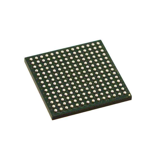
| 产品图片 |
|
| rohs | 符合RoHS无铅 / 符合限制有害物质指令(RoHS)规范要求 |
| 产品系列 | 嵌入式处理器和控制器,微控制器 - MCU,8位微控制器 -MCU,Microchip Technology PIC16F639-I/SSPIC® 16F |
| 数据手册 | http://www.microchip.com/mymicrochip/filehandler.aspx?ddocname=en019830http://www.microchip.com/mymicrochip/filehandler.aspx?ddocname=en020960http://www.microchip.com/mymicrochip/filehandler.aspx?ddocname=en531149点击此处下载产品Datasheethttp://www.microchip.com/mymicrochip/filehandler.aspx?ddocname=en013770点击此处下载产品Datasheethttp://www.microchip.com/mymicrochip/filehandler.aspx?ddocname=en541028http://www.microchip.com/mymicrochip/filehandler.aspx?ddocname=en012508 |
| 产品型号 | PIC16F639-I/SS |
| RAM容量 | 128 x 8 |
| 产品培训模块 | http://www.digikey.cn/PTM/IndividualPTM.page?site=cn&lang=zhs&ptm=2046http://www.digikey.cn/PTM/IndividualPTM.page?site=cn&lang=zhs&ptm=25053 |
| 产品目录页面 | |
| 产品种类 | 8位微控制器 -MCU |
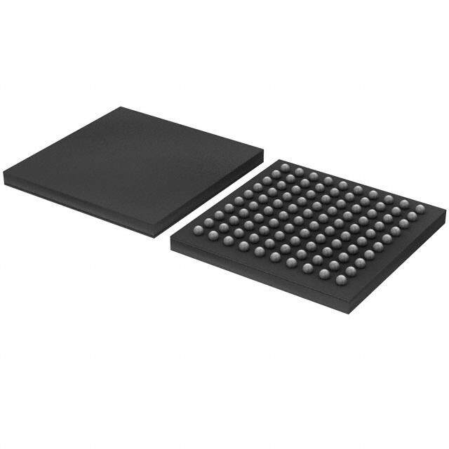
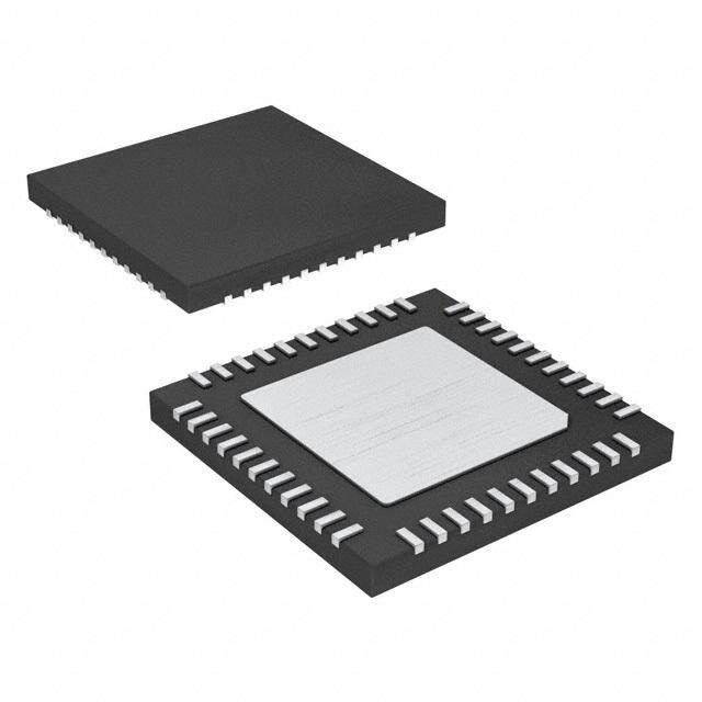
| 供应商器件封装 | 20-SSOP |
| 其它名称 | PIC16F639ISS |
| 包装 | 管件 |
| 可编程输入/输出端数量 | 12 |
| 商标 | Microchip Technology |
| 处理器系列 | PIC16 |
| 外设 | 欠压检测/复位,LVD,POR,WDT |
| 安装风格 | SMD/SMT |
| 定时器数量 | 2 Timer |
| 封装 | Tube |
| 封装/外壳 | 20-SSOP(0.209",5.30mm 宽) |
| 封装/箱体 | SSOP-20 |
| 工作温度 | -40°C ~ 85°C |
| 工作电源电压 | 2 V to 5.5 V |
| 工厂包装数量 | 67 |
| 振荡器类型 | 内部 |
| 接口类型 | SPI |
| 数据RAM大小 | 128 B |
| 数据Ram类型 | SRAM |
| 数据ROM大小 | 256 B |
| 数据Rom类型 | EEPROM |
| 数据总线宽度 | 8 bit |
| 数据转换器 | - |
| 最大工作温度 | + 85 C |
| 最大时钟频率 | 20 MHz |
| 最小工作温度 | - 40 C |
| 标准包装 | 67 |
| 核心 | PIC |
| 核心处理器 | PIC |
| 核心尺寸 | 8-位 |
| 片上ADC | No |
| 片上DAC | Without DAC |
| 电压-电源(Vcc/Vdd) | 2 V ~ 3.6 V |
| 电源电压-最大 | 5.5 V |
| 电源电压-最小 | 2 V |
| 程序存储器大小 | 2048 B |
| 程序存储器类型 | Flash |
| 程序存储容量 | 3.5KB(2K x 14) |
| 系列 | PIC16 |
| 输入/输出端数量 | 12 I/O |
| 连接性 | - |
| 速度 | 20MHz |
| 配用 | /product-detail/zh/AC162066/AC162066-ND/1015414/product-detail/zh/AC164307/AC164307-ND/613141 |


- 商务部:美国ITC正式对集成电路等产品启动337调查
- 曝三星4nm工艺存在良率问题 高通将骁龙8 Gen1或转产台积电
- 太阳诱电将投资9.5亿元在常州建新厂生产MLCC 预计2023年完工
- 英特尔发布欧洲新工厂建设计划 深化IDM 2.0 战略
- 台积电先进制程称霸业界 有大客户加持明年业绩稳了
- 达到5530亿美元!SIA预计今年全球半导体销售额将创下新高
- 英特尔拟将自动驾驶子公司Mobileye上市 估值或超500亿美元
- 三星加码芯片和SET,合并消费电子和移动部门,撤换高东真等 CEO
- 三星电子宣布重大人事变动 还合并消费电子和移动部门
- 海关总署:前11个月进口集成电路产品价值2.52万亿元 增长14.8%


PDF Datasheet 数据手册内容提取
PIC12F635/PIC16F636/639 Data Sheet 8/14-Pin, Flash-Based 8-Bit CMOS Microcontrollers with nanoWatt Technology *8-bit, 8-pin Devices Protected by Microchip’s Low Pin Count Patent: U. S. Patent No. 5,847,450. Additional U.S. and foreign patents and applications may be issued or pending. © 2007 Microchip Technology Inc. DS41232D
Note the following details of the code protection feature on Microchip devices: (cid:129) Microchip products meet the specification contained in their particular Microchip Data Sheet. (cid:129) Microchip believes that its family of products is one of the most secure families of its kind on the market today, when used in the intended manner and under normal conditions. (cid:129) There are dishonest and possibly illegal methods used to breach the code protection feature. All of these methods, to our knowledge, require using the Microchip products in a manner outside the operating specifications contained in Microchip’s Data Sheets. Most likely, the person doing so is engaged in theft of intellectual property. (cid:129) Microchip is willing to work with the customer who is concerned about the integrity of their code. (cid:129) Neither Microchip nor any other semiconductor manufacturer can guarantee the security of their code. Code protection does not mean that we are guaranteeing the product as “unbreakable.” Code protection is constantly evolving. We at Microchip are committed to continuously improving the code protection features of our products. Attempts to break Microchip’s code protection feature may be a violation of the Digital Millennium Copyright Act. If such acts allow unauthorized access to your software or other copyrighted work, you may have a right to sue for relief under that Act. Information contained in this publication regarding device Trademarks applications and the like is provided only for your convenience The Microchip name and logo, the Microchip logo, Accuron, and may be superseded by updates. It is your responsibility to dsPIC, KEELOQ, KEELOQ logo, microID, MPLAB, PIC, ensure that your application meets with your specifications. PICmicro, PICSTART, PROMATE, PowerSmart, rfPIC, and MICROCHIP MAKES NO REPRESENTATIONS OR SmartShunt are registered trademarks of Microchip WARRANTIES OF ANY KIND WHETHER EXPRESS OR Technology Incorporated in the U.S.A. and other countries. IMPLIED, WRITTEN OR ORAL, STATUTORY OR OTHERWISE, RELATED TO THE INFORMATION, AmpLab, FilterLab, Linear Active Thermistor, Migratable INCLUDING BUT NOT LIMITED TO ITS CONDITION, Memory, MXDEV, MXLAB, PS logo, SEEVAL, SmartSensor QUALITY, PERFORMANCE, MERCHANTABILITY OR and The Embedded Control Solutions Company are FITNESS FOR PURPOSE. Microchip disclaims all liability registered trademarks of Microchip Technology Incorporated arising from this information and its use. Use of Microchip in the U.S.A. devices in life support and/or safety applications is entirely at Analog-for-the-Digital Age, Application Maestro, CodeGuard, the buyer’s risk, and the buyer agrees to defend, indemnify and dsPICDEM, dsPICDEM.net, dsPICworks, ECAN, hold harmless Microchip from any and all damages, claims, ECONOMONITOR, FanSense, FlexROM, fuzzyLAB, suits, or expenses resulting from such use. No licenses are In-Circuit Serial Programming, ICSP, ICEPIC, Mindi, MiWi, conveyed, implicitly or otherwise, under any Microchip MPASM, MPLAB Certified logo, MPLIB, MPLINK, PICkit, intellectual property rights. PICDEM, PICDEM.net, PICLAB, PICtail, PowerCal, PowerInfo, PowerMate, PowerTool, REAL ICE, rfLAB, rfPICDEM, Select Mode, Smart Serial, SmartTel, Total Endurance, UNI/O, WiperLock and ZENA are trademarks of Microchip Technology Incorporated in the U.S.A. and other countries. SQTP is a service mark of Microchip Technology Incorporated in the U.S.A. All other trademarks mentioned herein are property of their respective companies. © 2007, Microchip Technology Incorporated, Printed in the U.S.A., All Rights Reserved. Printed on recycled paper. Microchip received ISO/TS-16949:2002 certification for its worldwide headquarters, design and wafer fabrication facilities in Chandler and Tempe, Arizona, Gresham, Oregon and Mountain View, California. The Company’s quality system processes and procedures are for its PIC® MCUs and dsPIC® DSCs, KEELOQ® code hopping devices, Serial EEPROMs, microperipherals, nonvolatile memory and analog products. In addition, Microchip’s quality system for the design and manufacture of development systems is ISO 9001:2000 certified. DS41232D-page ii © 2007 Microchip Technology Inc.
PIC12F635/PIC16F636/639 8/14-Pin Flash-Based, 8-Bit CMOS Microcontrollers With nanoWatt Technology High-Performance RISC CPU: Peripheral Features: (cid:129) Only 35 instructions to learn: (cid:129) 6/12 I/O pins with individual direction control: - All single-cycle instructions except branches - High-current source/sink for direct LED drive (cid:129) Operating speed: - Interrupt-on-change pin - DC – 20MHz oscillator/clock input - Individually programmable weak pull-ups/ - DC – 200ns instruction cycle pull-downs (cid:129) Interrupt capability - Ultra Low-Power Wake-up (cid:129) 8-level deep hardware stack (cid:129) Analog Comparator module with: (cid:129) Direct, Indirect and Relative Addressing modes - Up to two analog comparators Special Microcontroller Features: - Programmable On-chip Voltage Reference (CVREF) module (% of VDD) (cid:129) Precision Internal Oscillator: - Comparator inputs and outputs externally - Factory calibrated to ±1%, typical accessible - Software selectable frequency range of (cid:129) Timer0: 8-bit timer/counter with 8-bit 8MHz to 125kHz programmable prescaler - Software tunable (cid:129) Enhanced Timer1: - Two-Speed Start-up mode - 16-bit timer/counter with prescaler - Crystal fail detect for critical applications - External Timer1 Gate (count enable) - Clock mode switching during operation for - Option to use OSC1 and OSC2 in LP mode power savings as Timer1 oscillator if INTOSC mode (cid:129) Clock mode switching for low-power operation selected (cid:129) Power-Saving Sleep mode (cid:129) K EELOQ® compatible hardware Cryptographic (cid:129) Wide operating voltage range (2.0V-5.5V) module (cid:129) Industrial and Extended Temperature range (cid:129) In-Circuit Serial Programming™ (ICSP™) via (cid:129) Power-on Reset (POR) two pins (cid:129) Wake-up Reset (WUR) (cid:129) Independent weak pull-up/pull-down resistors Low-Frequency Analog Front-End (cid:129) Programmable Low-Voltage Detect (PLVD) Features (PIC16F639 only): (cid:129) Power-up Timer (PWRT) and Oscillator Start-up (cid:129) Three input pins for 125kHz LF input signals Timer (OST) (cid:129) High input detection sensitivity (3mV PP, typical) (cid:129) Brown-out Reset (BOR) with software control (cid:129) Demodulated data, Carrier clock or RSSI output option selection (cid:129) Enhanced Low-Current Watchdog Timer (WDT) (cid:129) Input carrier frequency: 125kHz, typical with on-chip oscillator (software selectable (cid:129) Input modulation frequency: 4kHz, maximum nominal 268 seconds with full prescaler) with (cid:129) 8 internal Configuration registers software enable (cid:129) Bidirectional transponder communication (cid:129) Multiplexed Master Clear with pull-up/input pin (LF talk back) (cid:129) Programmable code protection (program and (cid:129) Programmable antenna tuning capacitance data independent) (up to 63pF, 1 pF/step) (cid:129) High-Endurance Flash/EEPROM cell: (cid:129) Low standby current: 5 μA (with 3 channels - 100,000 write Flash endurance enabled), typical - 1,000,000 write EEPROM endurance (cid:129) Low operating current: 15 μA (with 3 channels - Flash/Data EEPROM Retention: > 40 years enabled), typical (cid:129) Serial Peripheral Interface (SPI) with internal Low-Power Features: MCU and external devices (cid:129) Standby Current: (cid:129) Supports Battery Back-up mode and batteryless - 1nA @ 2.0V, typical operation with external circuits (cid:129) Operating Current: - 8.5μA @ 32kHz, 2.0V, typical - 100μA @ 1MHz, 2.0V, typical (cid:129) Watchdog Timer Current: - 1μA @ 2.0V, typical © 2007 Microchip Technology Inc. DS41232D-page 1
PIC12F635/PIC16F636/639 Program Memory Data Memory Low Frequency Device I/O Comparators Analog Flash (words) SRAM (bytes) EEPROM (bytes) Front-End PIC12F635 1024 64 128 6 1 N PIC16F636 2048 128 256 12 2 N PIC16F639 2048 128 256 12 2 Y Note 1: Any references to PORTA, RAn, TRISA and TRISAn refer to GPIO, GPn, TRISIO and TRISIOn, respectively. 2: VDDT is the supply voltage of the Analog Front-End section (PIC16F639 only). VDDT is treated as VDD in this document unless otherwise stated. 3: VSST is the ground reference voltage of the Analog Front-End section (PIC16F639 only). VSST is treated as VSS in this document unless otherwise stated. DS41232D-page 2 © 2007 Microchip Technology Inc.
PIC12F635/PIC16F636/639 8-Pin Diagrams (PDIP, SOIC, DFN, DFN-S) PDIP, SOIC VDD 1 8 VSS 5 GP5/T1CKI/OSC1/CLKIN 2 63 7 GP0/C1IN+/ICSPDAT/ULPWU F 2 GP4/T1G/OSC2/CLKOUT 3 C1 6 GP1/C1IN-/ICSPCLK PI GP3/MCLR/VPP 4 5 GP2/T0CKI/INT/C1OUT DFN, DFN-S VDD 1 5 8 VSS 3 GP5/T1CKI/OSC1/CLKIN 2 6 7 GP0/CIN+/ICSPDAT/ULPWU F GP4/T1G/OSC2/CLKOUT 3 12 6 GP1/CIN-/ICSPCLK C GP3/MCLR/VDD 4 PI 5 GP2/T0CKI/INT/COUT TABLE 1: 8-PIN SUMMARY (PDIP, SOIC, DFN, DFN-S) I/O Pin Comparators Timer Interrupts Pull-ups Basic GP0 7 C1IN+ — IOC Y ICSPDAT/ULPWU GP1 6 C1IN- — IOC Y ICSPCLK GP2 5 C1OUT T0CKI INT/IOC Y — GP3(1) 4 — — IOC Y(2) MCLR/VPP GP4 3 — T1G IOC Y OSC2/CLKOUT GP5 2 — T1CKI IOC Y OSC1/CLKIN — 1 — — — — VDD — 8 — — — — VSS Note 1: Input only. 2: Only when pin is configured for external MCLR. © 2007 Microchip Technology Inc. DS41232D-page 3
PIC12F635/PIC16F636/639 14-Pin Diagram (PDIP, SOIC, TSSOP) VDD 1 14 VSS RA5/T1CKI/OSC1/CLKIN 2 13 RA0/C1IN+/ICSPDAT/ULPWU 6 RA4/T1G/OSC2/CLKOUT 3 3 12 RA1/C1IN-/VREF/ICSPCLK 6 RA3/MCLR/VPP 4 6F 11 RA2/T0CKI/INT/C1OUT 1 RC5 5 C 10 RC0/C2IN+ RC4/C2OUT 6 PI 9 RC1/C2IN- RC3 7 8 RC2 TABLE 2: 14-PIN SUMMARY (PDIP, SOIC, TSSOP) I/O Pin Comparators Timer Interrupts Pull-ups Basic RA0 13 C1IN+ — IOC Y ICSPDAT/ULPWU RA1 12 C1IN- — IOC Y VREF/ICSPCLK RA2 11 C1OUT T0CKI INT/IOC Y — RA3(1) 4 — — IOC Y(2) MCLR/VPP RA4 3 — T1G IOC Y OSC2/CLKOUT RA5 2 — T1CKI IOC Y OSC1/CLKIN RC0 10 C2IN+ — — — — RC1 9 C2IN- — — — — RC2 8 — — — — — RC3 7 — — — — — RC4 6 C2OUT — — — — RC5 5 — — — — — — 1 — — — — VDD — 14 — — — — VSS Note 1: Input only. 2: Only when pin is configured for external MCLR. DS41232D-page 4 © 2007 Microchip Technology Inc.
PIC12F635/PIC16F636/639 16-Pin Diagram QFN DD C C SS V N N V 6 5 4 3 1 1 1 1 RA5/T1CKI/OSC1/CLKIN 1 12 RA0/C1IN+/ICSPDAT/ULPWU RA4/AN3/T1G/OSC2/CLKOUT 2 11 RA1/C1IN-/VREF/ICSPCLK PIC16F636 RA3/MCLR/VPP 3 10 RA2/T0CKI/INT/C1OUT RC5 4 9 RC0/C2IN+ 5 6 7 8 UT C3 C2 N- O R R 2I 2 C C 1/ 4/ C C R R TABLE 3: 16-PIN SUMMARY I/O Pin Comparators Timer Interrupts Pull-ups Basic RA0 12 C1IN+ — IOC Y ICSPDAT/ULPWU RA1 11 C1IN- — IOC Y VREF/ICSPCLK RA2 10 C1OUT T0CKI INT/IOC Y — RA3(1) 3 — — IOC Y(2) MCLR/VPP RA4 2 — T1G IOC Y OSC2/CLKOUT RA5 1 — T1CKI IOC Y OSC1/CLKIN RC0 9 C2IN+ — — — — RC1 8 C2IN- — — — — RC2 7 — — — — — RC3 6 — — — — — RC4 5 C2OUT — — — — RC5 4 — — — — — — 16 — — — — VDD — 13 — — — — VSS — 14 — — — — NC — 15 — — — — NC Note 1: Input only. 2: Only when pin is configured for external MCLR. © 2007 Microchip Technology Inc. DS41232D-page 5
PIC12F635/PIC16F636/639 20-Pin Diagram SSOP VDD 1 20 VSS RA5/T1CKI/OSC1/CLKIN 2 19 RA0/C1IN+/ICSPDAT/ULPWU RA4/T1G/OSC2/CLKOUT 3 18 RA1/C1IN-/VREF/ICSPCLK RA3/MCLR/VPP 4 9 17 RA2/TOCKI/INT/C1OUT 3 RC5 5 F6 16 RC0/C2IN+ 6 RC4/C2OUT 6 1 15 RC1/C2IN-/CS C RC3/LFDATA/RSSI/CCLK/SDIO 7 PI 14 RC2/SCLK/ALERT VDDT(3) 8 13 VSST(4) LCZ 9 12 LCCOM LCY 10 11 LCX TABLE 4: 20-PIN SUMMARY I/O Pin Analog Front-End Comparators Timer Interrupts Pull-ups Basic RA0 19 — C1IN+ — IOC Y ICSPDAT/ULPWU RA1 18 — C1IN- — IOC Y VREF/ICSPCLK RA2 17 — C1OUT T0CKI INT/IOC Y — RA3(1) 4 — — — IOC Y(2) MCLR/VPP RA4 3 — — T1G IOC Y OSC2/CLKOUT RA5 2 — — T1CKI IOC Y OSC1/CLKIN RC0 16 — C2IN+ — — — — RC1 15 — C2IN- — — — CS RC2 14 ALERT — — — — SCLK RC3 7 LFDATA/RSSI — — — — CCLK/SDIO RC4 6 — C2OUT — — — — RC5 5 — — — — — — — 8 — — — — — VDDT(3) — 13 — — — — — VSST(4) — 11 LCX — — — — — — 10 LCY — — — — — — 9 LCZ — — — — — — 12 LCCOM — — — — — — 1 — — — — — VDD — 20 — — — — — VSS Note 1: Input only. 2: Only when pin is configured for external MCLR. 3: VDDT is the supply voltage of the Analog Front-End section (PIC16F639 only). VDDT is treated as VDD in this document unless otherwise stated. 4: VSST is the ground reference voltage of the Analog Front-End section (PIC16F639 only). VSST is treated as VSS in this document unless otherwise stated. DS41232D-page 6 © 2007 Microchip Technology Inc.
PIC12F635/PIC16F636/639 Table of Contents 1.0 Device Overview..........................................................................................................................................................................9 2.0 Memory Organization.................................................................................................................................................................17 3.0 Clock Sources............................................................................................................................................................................35 4.0 I/O Ports.....................................................................................................................................................................................47 5.0 Timer0 Module...........................................................................................................................................................................61 6.0 Timer1 Module with Gate Control...............................................................................................................................................64 7.0 Comparator Module....................................................................................................................................................................71 8.0 Programmable Low-Voltage Detect (PLVD) Module..................................................................................................................87 9.0 Data EEPROM Memory.............................................................................................................................................................91 10.0 KEELOQ® Compatible Cryptographic Module.............................................................................................................................95 11.0 Analog Front-End (AFE) Functional Description (PIC16F639 Only)..........................................................................................97 12.0 Special Features of the CPU....................................................................................................................................................129 13.0 Instruction Set Summary..........................................................................................................................................................149 14.0 Development Support...............................................................................................................................................................159 15.0 Electrical Specifications............................................................................................................................................................163 16.0 DC and AC Characteristics Graphs and Tables.......................................................................................................................191 17.0 Packaging Information..............................................................................................................................................................211 On-Line Support 223 Systems Information and Upgrade Hot Line..................................................................................................................................... 223 Reader Response............................................................................................................................................................................. 224 Appendix A: Data Sheet Revision History......................................................................................................................................... 225 Product Identification System........................................................................................................................................................... 231 Worldwide Sales and Service........................................................................................................................................................... 232 TO OUR VALUED CUSTOMERS It is our intention to provide our valued customers with the best documentation possible to ensure successful use of your Microchip products. To this end, we will continue to improve our publications to better suit your needs. Our publications will be refined and enhanced as new volumes and updates are introduced. If you have any questions or comments regarding this publication, please contact the Marketing Communications Department via E-mail at docerrors@microchip.com or fax the Reader Response Form in the back of this data sheet to (480) 792-4150. We welcome your feedback. Most Current Data Sheet To obtain the most up-to-date version of this data sheet, please register at our Worldwide Web site at: http://www.microchip.com You can determine the version of a data sheet by examining its literature number found on the bottom outside corner of any page. The last character of the literature number is the version number, (e.g., DS30000A is version A of document DS30000). Errata An errata sheet, describing minor operational differences from the data sheet and recommended workarounds, may exist for current devices. As device/documentation issues become known to us, we will publish an errata sheet. The errata will specify the revision of silicon and revision of document to which it applies. To determine if an errata sheet exists for a particular device, please check with one of the following: (cid:129) Microchip’s Worldwide Web site; http://www.microchip.com (cid:129) Your local Microchip sales office (see last page) When contacting a sales office, please specify which device, revision of silicon and data sheet (include literature number) you are using. Customer Notification System Register on our web site at www.microchip.com to receive the most current information on all of our products. © 2007 Microchip Technology Inc. DS41232D-page 7
PIC12F635/PIC16F636/639 NOTES: DS41232D-page 8 © 2007 Microchip Technology Inc.
PIC12F635/PIC16F636/639 1.0 DEVICE OVERVIEW Block Diagrams and pinout descriptions of the devices are as follows: This document contains device specific information for (cid:129) PIC12F635 (Figure1-1, Table1-1) the PIC12F635/PIC16F636/639 devices. (cid:129) PIC16F636 (Figure1-2, Table1-2) (cid:129) PIC16F639 (Figure1-3, Table1-3) FIGURE 1-1: PIC12F635 BLOCK DIAGRAM Configuration 13 Data Bus 8 GPIO Program Counter GP0 Flash GP1 1K x 14 Program RAM GP2 Memory 8-level Stack 64 bytes GP3 (13-bit) File GP4 Registers GP5 Program 14 Bus RAM Addr 9 Addr MUX Instruction Reg Direct Addr 7 Indirect 8 Addr FSR Reg STATUS Reg 8 3 Power-up MUX Instruction Timer Decode and Oscillator Control Start-up Timer Power-on ALU OSC1/CLKIN Reset 8 Timing Watchdog Generation Timer W Reg Brown-out OSC2/CLKOUT Reset Programmable 8 MHz 31 kHz Low-Voltage Detect Internal Internal Oscillator Oscillator Wake-up Reset T1G MCLR VDD VSS T1CKI Timer0 Timer1 T0CKI Cryptographic 1 Analog Module Comparator EEDAT and Reference 128 bytes Data EEPROM EEADDR C1IN-C1IN+C1OUT © 2007 Microchip Technology Inc. DS41232D-page 9
PIC12F635/PIC16F636/639 FIGURE 1-2: PIC16F636 BLOCK DIAGRAM Configuration 13 8 Data Bus PORTA Program Counter RA0 Flash 2K x 14 RA1 Program RAM RA2 Memory 8-level Stack 128 RA3 bytes (13-bit) RA4 File Registers RA5 Program 14 Bus RAM Addr 9 Addr MUX Instruction Reg PORTC Direct Addr 7 Indirect 8 Addr RC0 RC1 FSR Reg RC2 STATUS Reg RC3 8 RC4 RC5 3 Power-up MUX Timer Oscillator Instruction Start-up Timer Decode and Control Power-on ALU Reset 8 OSC1/CLKIN Watchdog Timer Timing W Reg Generation Brown-out Reset OSC2/CLKOUT Programmable Low-Voltage Detect 8 MHz 31 kHz Wake-up Internal Internal Reset T1CKI T1G Oscillator Oscillator MCLR VDD VSS Timer0 Timer1 T0CKI Cryptographic 2 Analog Comparators EEDAT and Reference Module 256 bytes Data EEPROM EEADDR C1IN- C1IN+ C1OUT C2IN- C2IN+ C2OUT DS41232D-page 10 © 2007 Microchip Technology Inc.
PIC12F635/PIC16F636/639 FIGURE 1-3: PIC16F639 BLOCK DIAGRAM Configuration PORTA 13 8 Data Bus Program Counter RA0 Flash RA1 2K x 14 Program RAM RA2 Memory 8-level Stack 128 RA3 bytes (13-bit) File RA4 Registers Program RA5 Bus 14 RAM Addr (1) 9 Addr MUX Instruction Reg PORTC Direct Addr 7 8 InAddirderct RC0 RC1 FSR Reg RC2 STATUS Reg RC3 8 RC4 RC5 3 Power-up MUX Timer Oscillator Instruction Start-up Timer DeCcoodnetr oalnd Power-on ALU Reset 8 OSC1/CLKIN Watchdog Timer Timing W Reg Generation Brown-out VDDT Reset 125kHz OSC2/CLKOUT Programmable VSST Analog Front-End Low-voltage Detect (AFE) 8 MHz 31 kHz Wake-up LCCOM Internal Internal Reset T1CKI T1G Oscillator Oscillator LCX LCY LCZ MCLR VDD VSS Timer0 Timer1 T0CKI 2 Analog KEELOQ Module Comparators EEDAT and Reference 256 bytes DATA EEPROM EEADDR C1IN- C1IN+C1OUTC2IN- C2IN+C2OUT © 2007 Microchip Technology Inc. DS41232D-page 11
PIC12F635/PIC16F636/639 TABLE 1-1: PIC12F635 PINOUT DESCRIPTIONS Input Output Name Function Description Type Type GP0/C1IN+/ICSPDAT/ULPWU GP0 TTL — General purpose I/O. Individually controlled interrupt-on-change. Individually enabled pull-up/pull-down. Selectable Ultra Low-Power Wake-up pin. C1IN+ AN — Comparator 1 input – positive. ICSPDAT TTL CMOS Serial programming data I/O. ULPWU AN — Ultra Low-Power Wake-up input. GP1/C1IN-/ICSPCLK GP1 TTL CMOS General purpose I/O. Individually controlled interrupt-on-change. Individually enabled pull-up/pull-down. C1IN- AN — Comparator 1 input – negative. ICSPCLK ST — Serial programming clock. GP2/T0CKI/INT/C1OUT GP2 ST CMOS General purpose I/O. Individually controlled interrupt-on-change. Individually enabled pull-up/pull-down. T0CKI ST — External clock for Timer0. INT ST — External interrupt. C1OUT — CMOS Comparator 1 output. GP3/MCLR/VPP GP3 TTL — General purpose input. Individually controlled interrupt-on-change. MCLR ST — Master Clear Reset. Pull-up enabled when configured as MCLR. VPP HV — Programming voltage. GP4/T1G/OSC2/CLKOUT GP4 TTL CMOS General purpose I/O. Individually controlled interrupt-on-change. Individually enabled pull-up/pull-down. T1G ST — Timer1 gate. OSC2 — XTAL XTAL connection. CLKOUT — CMOS TOSC/4 reference clock. GP5/T1CKI/OSC1/CLKIN GP5 TTL CMOS General purpose I/O. Individually controlled interrupt-on-change. Individually enabled pull-up/pull-down. T1CKI ST — Timer1 clock. OSC1 XTAL — XTAL connection. CLKIN ST — TOSC reference clock. VDD VDD D — Power supply for microcontroller. VSS VSS D — Ground reference for microcontroller. Legend: AN = Analog input or output CMOS = CMOS compatible input or output D = Direct HV = High Voltage ST = Schmitt Trigger input with CMOS levels TTL = TTL compatible input XTAL = Crystal DS41232D-page 12 © 2007 Microchip Technology Inc.
PIC12F635/PIC16F636/639 TABLE 1-2: PIC16F636 PINOUT DESCRIPTIONS Input Output Name Function Description Type Type RA0/C1IN+/ICSPDAT/ULPWU RA0 TTL — General purpose I/O. Individually controlled interrupt-on-change. Individually enabled pull-up/pull-down. Selectable Ultra Low-Power Wake-up pin. C1IN+ AN — Comparator 1 input – positive. ICSPDAT TTL CMOS Serial programming data I/O. ULPWU AN — Ultra Low-Power Wake-up input. RA1/C1IN-/VREF/ICSPCLK RA1 TTL CMOS General purpose I/O. Individually controlled interrupt-on-change. Individually enabled pull-up/pull-down. C1IN- AN — Comparator 1 input – negative. VREF AN — External voltage reference ICSPCLK ST — Serial programming clock. RA2/T0CKI/INT/C1OUT RA2 ST CMOS General purpose I/O. Individually controlled interrupt-on-change. Individually enabled pull-up/pull-down. T0CKI ST — External clock for Timer0. INT ST — External interrupt. C1OUT — CMOS Comparator 1 output. RA3/MCLR/VPP RA3 TTL — General purpose input. Individually controlled interrupt-on-change. MCLR ST — Master Clear Reset. Pull-up enabled when configured as MCLR. VPP HV — Programming voltage. RA4/T1G/OSC2/CLKOUT RA4 TTL CMOS General purpose I/O. Individually controlled interrupt-on-change. Individually enabled pull-up/pull-down. T1G ST — Timer1 gate. OSC2 — XTAL XTAL connection. CLKOUT — CMOS TOSC/4 reference clock. RA5/T1CKI/OSC1/CLKIN RA5 TTL CMOS General purpose I/O. Individually controlled interrupt-on-change. Individually enabled pull-up/pull-down. T1CKI ST — Timer1 clock. OSC1 XTAL — XTAL connection. CLKIN ST — TOSC reference clock. RC0/C2IN+ RC0 TTL CMOS General purpose I/O. C2IN+ AN — Comparator 1 input – positive. RC1/C2IN- RC1 TTL CMOS General purpose I/O. C2IN- AN — Comparator 1 input – negative. RC2 RC2 TTL CMOS General purpose I/O. RC3 RC3 TTL CMOS General purpose I/O. RC4/C2OUT RC4 TTL CMOS General purpose I/O. C2OUT — CMOS Comparator 2 output. RC5 RC5 TTL CMOS General purpose I/O. VDD VDD D — Power supply for microcontroller. VSS VSS D — Ground reference for microcontroller. Legend: AN = Analog input or output CMOS = CMOS compatible input or output D = Direct HV = High Voltage ST = Schmitt Trigger input with CMOS levels TTL = TTL compatible input XTAL = Crystal © 2007 Microchip Technology Inc. DS41232D-page 13
PIC12F635/PIC16F636/639 TABLE 1-3: PIC16F639 PINOUT DESCRIPTIONS Input Output Name Function Description Type Type LCCOM LCCOM AN — Common reference for analog inputs. LCX LCX AN — 125kHz analog X channel input. LCY LCY AN — 125kHz analog Y channel input. LCZ LCZ AN — 125kHz analog Z channel input. RA0/C1IN+/ICSPDAT/ULPWU RA0 TTL — General purpose I/O. Individually controlled interrupt-on-change. Individually enabled pull-up/pull-down. Selectable Ultra Low-Power Wake-up pin. C1IN+ AN — Comparator1 input – positive. ICSPDAT TTL CMOS Serial Programming Data IO. ULPWU AN — Ultra Low-Power Wake-up input. RA1/C1IN-/VREF/ICSPCLK RA1 TTL CMOS General purpose I/O. Individually controlled interrupt-on-change. Individually enabled pull-up/pull-down. C1IN- AN — Comparator1 input – negative. VREF AN — External voltage reference ICSPCLK ST — Serial Programming Clock. RA2/T0CKI/INT/C1OUT RA2 ST CMOS General purpose I/O. Individually controlled interrupt-on-change. Individually enabled pull-up/pull-down. T0CKI ST — External clock for Timer0. INT ST — External Interrupt. C1OUT — CMOS Comparator1 output. RA3/MCLR/VPP RA3 TTL — General purpose input. Individually controlled interrupt-on-change. MCLR ST — Master Clear Reset. Pull-up enabled when configured as MCLR. VPP HV — Programming voltage. RA4/T1G/OSC2/CLKOUT RA4 TTL CMOS General purpose I/O. Individually controlled interrupt-on-change. Individually enabled pull-up/pull-down. T1G ST — Timer1 gate. OSC2 — XTAL XTAL connection. CLKOUT — CMOS TOSC reference clock. RA5/T1CKI/OSC1/CLKIN RA5 TTL CMOS General purpose I/O. Individually controlled interrupt-on-change. Individually enabled pull-up/pull-down. T1CKI ST — Timer1 clock. OSC1 XTAL — XTAL connection. CLKIN ST — TOSC/4 reference clock. RC0/C2IN+ RC0 TTL CMOS General purpose I/O. C2IN+ AN — Comparator1 input – positive. RC1/C2IN-/CS RC1 TTL CMOS General purpose I/O. C2IN- AN — Comparator1 input – negative. CS TTL — Chip select input for SPI communication with internal pull-up resistor. RC2/SCLK/ALERT RC2 TTL CMOS General purpose I/O. SCLK TTL — Digital clock input for SPI communication. ALERT — OD Output with internal pull-up resistor for AFE error signal. Legend: AN = Analog input or output CMOS = CMOS compatible input or output D = Direct HV = High Voltage ST = Schmitt Trigger input with CMOS levels OD = Open Drain TTL = TTL compatible input XTAL = Crystal DS41232D-page 14 © 2007 Microchip Technology Inc.
PIC12F635/PIC16F636/639 TABLE 1-3: PIC16F639 PINOUT DESCRIPTIONS (CONTINUED) Input Output Name Function Description Type Type RC3/LFDATA/RSSI/CCLK/SDO RC3 TTL CMOS General purpose I/O. LFDATA — CMOS Digital output representation of analog input signal to LC pins. RSSI — Current Received signal strength indicator. Analog current that is proportional to input amplitude. CCLK — — Carrier clock output. SDIO TTL CMOS Input/Output for SPI communication. RC4/C2OUT RC4 TTL CMOS General purpose I/O. C2OUT — CMOS Comparator2 output. RC5 RC5 TTL CMOS General purpose I/O. VDDT VDDT D — Power supply for Analog Front-End. In this document, VDDT is treated the same as VDD, unless otherwise stated. VSST VSST D — Ground reference for Analog Front-End. In this document, VSST is treated the same as VSS, unless otherwise stated. VDD VDD D — Power supply for microcontroller. VSS VSS D — Ground reference for microcontroller. Legend: AN = Analog input or output CMOS = CMOS compatible input or output D = Direct HV = High Voltage ST = Schmitt Trigger input with CMOS levels OD = Open Drain TTL = TTL compatible input XTAL = Crystal © 2007 Microchip Technology Inc. DS41232D-page 15
PIC12F635/PIC16F636/639 NOTES: DS41232D-page 16 © 2007 Microchip Technology Inc.
PIC12F635/PIC16F636/639 2.0 MEMORY ORGANIZATION FIGURE 2-1: PROGRAM MEMORY MAP AND STACK OF THE PIC12F635 2.1 Program Memory Organization PC<12:0> The PIC12F635/PIC16F636/639 devices have a 13-bit CALL, RETURN RETFIE, RETLW 13 program counter capable of addressing an 8K x 14 program memory space. Only the first 1Kx14 (0000h-03FFh, for the PIC12F635) and 2Kx14 Stack Level 1 (0000h-07FFh, for the PIC16F636/639) is physically implemented. Accessing a location above these boundaries will cause a wraparound within the first Stack Level 8 2Kx14 space. The Reset vector is at 0000h and the interrupt vector is at 0004h (see Figure2-1). Reset Vector 0000h 2.2 Data Memory Organization Interrupt Vector 0004h The data memory (see Figure2-2) is partitioned into 0005h two banks, which contain the General Purpose Registers (GPR) and the Special Function Registers On-chip Program Memory (SFR). The Special Function Registers are located in the first 32 locations of each bank. Register locations 03FFh 20h-7Fh in Bank 0 and A0h-BFh in Bank 1 are GPRs, implemented as static RAM for the PIC16F636/639. 0400h For the PIC12F635, register locations 40h through 7Fh Access 0-3FFh are GPRs implemented as static RAM. Register locations F0h-FFh in Bank 1 point to addresses 1FFFh 70h-7Fh in Bank0. All other RAM is unimplemented and returns ‘0’ when read. RP0 of the STATUS register FIGURE 2-2: PROGRAM MEMORY MAP AND is the bank select bit. STACK OF THE PIC16F636/639 RP1 RP0 PC<12:0> 0 0 → Bank 0 is selected CALL, RETURN 0 1 → Bank 1 is selected RETFIE, RETLW 13 1 0 → Bank 2 is selected Stack Level 1 1 1 → Bank 3 is selected Stack Level 8 Reset Vector 0000h Interrupt Vector 0004h 0005h On-chip Program Memory 07FFh 0800h Access 0-7FFh 1FFFh © 2007 Microchip Technology Inc. DS41232D-page 17
PIC12F635/PIC16F636/639 2.2.1 GENERAL PURPOSE REGISTER The register file is organized as 64 x 8 for the PIC12F635 and 128 x 8 for the PIC16F636/639. Each register is accessed, either directly or indirectly, through the File Select Register, FSR (see Section2.4 “Indirect Addressing, INDF and FSR Registers”). 2.2.2 SPECIAL FUNCTION REGISTERS The Special Function Registers (SFRs) are registers used by the CPU and peripheral functions for controlling the desired operation of the device (see Figure2-1). These registers are static RAM. The special registers can be classified into two sets: core and peripheral. The Special Function Registers associated with the “core” are described in this section. Those related to the operation of the peripheral features are described in the section of that peripheral feature. DS41232D-page 18 © 2007 Microchip Technology Inc.
PIC12F635/PIC16F636/639 FIGURE 2-3: PIC12F635 SPECIAL FUNCTION REGISTERS File File File File Address Address Address Address Indirect addr.(1) 00h Indirect addr.(1) 80h Accesses 100h Accesses 180h TMR0 01h OPTION_REG 81h 00h-0Bh 101h 80h-8Bh 181h PCL 02h PCL 82h 102h 182h STATUS 03h STATUS 83h 103h 183h FSR 04h FSR 84h 104h 184h GPIO 05h TRISIO 85h 105h 185h 06h 86h 106h 186h 07h 87h 107h 187h 08h 88h 108h 188h 09h 89h 109h 189h PCLATH 0Ah PCLATH 8Ah 10Ah 18Ah INTCON 0Bh INTCON 8Bh 10Bh 18Bh PIR1 0Ch PIE1 8Ch 10Ch 18Ch 0Dh 8Dh 10Dh 18Dh TMR1L 0Eh PCON 8Eh 10Eh 18Eh TMR1H 0Fh OSCCON 8Fh 10Fh 18Fh T1CON 10h OSCTUNE 90h CRCON 110h 190h 11h 91h CRDAT0(2) 111h 191h 12h 92h CRDAT1(2) 112h 192h 13h 93h CRDAT2(2) 113h 193h 14h LVDCON 94h CRDAT3(2) 114h 194h 15h WPUDA 95h 115h 195h 16h IOCA 96h 116h 196h 17h WDA 97h 117h 197h WDTCON 18h 98h 118h 198h CMCON0 19h VRCON 99h 119h 199h CMCON1 1Ah EEDAT 9Ah 11Ah 19Ah 1Bh EEADR 9Bh 11Bh 19Bh 1Ch EECON1 9Ch 11Ch 19Ch 1Dh EECON2(1) 9Dh 11Dh 19Dh 1Eh 9Eh 11Eh 19Eh 1Fh 9Fh 11Fh 19Fh 20h A0h 120h 1A0h 3Fh General 40h Purpose Register EFh 16Fh 1EFh 64 Bytes Accesses F0h Accesses 170h Accesses 1F0h 7Fh 70h-7Fh FFh 70h-7Fh 17Fh Bank 0 1FFh Bank 0 Bank 1 Bank 2 Bank 3 Unimplemented data memory locations, read as ‘0’. Note1: Not a physical register. 2: CRDAT<3:0> registers are KEELOQ® hardware peripheral related registers and require the execution of the “KEELOQ® Encoder License Agreement” regarding implementation of the module and access to related registers. The “KEELOQ® Encoder License Agreement” may be accessed through the Microchip web site located at www.microchip.com/KEELOQ or by contacting your local Microchip Sales Representative. © 2007 Microchip Technology Inc. DS41232D-page 19
PIC12F635/PIC16F636/639 FIGURE 2-4: PIC16F636/639 SPECIAL FUNCTION REGISTERS File File File File Address Address Address Address Indirect addr.(1) 00h Indirect addr. (1) 80h Accesses 100h Accesses 180h TMR0 01h OPTION_REG 81h 00h-0Bh 101h 80h-8Bh 181h PCL 02h PCL 82h 102h 182h STATUS 03h STATUS 83h 103h 183h FSR 04h FSR 84h 104h 184h PORTA 05h TRISA 85h 105h 185h 06h 86h 106h 186h PORTC 07h TRISC 87h 107h 187h 08h 88h 108h 188h 09h 89h 109h 189h PCLATH 0Ah PCLATH 8Ah 10Ah 18Ah INTCON 0Bh INTCON 8Bh 10Bh 18Bh PIR1 0Ch PIE1 8Ch 10Ch 18Ch 0Dh 8Dh 10Dh 18Dh TMR1L 0Eh PCON 8Eh 10Eh 18Eh TMR1H 0Fh OSCCON 8Fh 10Fh 18Fh T1CON 10h OSCTUNE 90h CRCON 110h 190h 11h 91h CRDAT0(2) 111h 191h 12h 92h CRDAT1(2) 112h 192h 13h 93h CRDAT2(2) 113h 193h 14h LVDCON 94h CRDAT3(2) 114h 194h 15h WPUDA 95h 115h 195h 16h IOCA 96h 116h 196h 17h WDA 97h 117h 197h WDTCON 18h 98h 118h 198h CMCON0 19h VRCON 99h 119h 199h CMCON1 1Ah EEDAT 9Ah 11Ah 19Ah 1Bh EEADR 9Bh 11Bh 19Bh 1Ch EECON1 9Ch 11Ch 19Ch 1Dh EECON2(1) 9Dh 11Dh 19Dh 1Eh 9Eh 11Eh 19Eh 1Fh 9Fh 11Fh 19Fh General 20h General A0h 120h 1A0h Purpose Purpose Register Register 96 Bytes 32 Bytes BFh C0h EFh 16Fh 1EFh Accesses F0h Accesses 170h Accesses 1F0h 7Fh 70h-7Fh FFh 70h-7Fh 17Fh Bank 0 1FFh Bank 0 Bank 1 Bank 2 Bank 3 Unimplemented data memory locations, read as ‘0’. Note1: Not a physical register. 2: CRDAT<3:0> registers are KEELOQ hardware peripheral related registers and require the execution of the “KEELOQ® Encoder License Agreement” regarding implementation of the module and access to related registers. The “KEELOQ® Encoder License Agreement” may be accessed through the Microchip web site located at www.microchip.com/KEELOQ or by contacting your local Microchip Sales Representative. DS41232D-page 20 © 2007 Microchip Technology Inc.
PIC12F635/PIC16F636/639 TABLE 2-1: PIC12F635 SPECIAL FUNCTION REGISTERS SUMMARY BANK 0 Value on Addr Name Bit 7 Bit 6 Bit 5 Bit 4 Bit 3 Bit 2 Bit 1 Bit 0 POR/BOR/ Page WUR Bank 0 00h INDF Addressing this location uses contents of FSR to address data memory xxxx xxxx 32,137 (not a physical register) 01h TMR0 Timer0 Module Register xxxx xxxx 61,137 02h PCL Program Counter’s (PC) Least Significant Byte 0000 0000 32,137 03h STATUS IRP RP1 RP0 TO PD Z DC C 0001 1xxx 26,137 04h FSR Indirect Data Memory Address Pointer xxxx xxxx 32,137 05h GPIO — — GP5 GP4 GP3 GP2 GP1 GP0 --xx xx00 47,137 06h — Unimplemented — — 07h — Unimplemented — — 08h — Unimplemented — — 09h — Unimplemented — — 0Ah PCLATH — — — Write Buffer for upper 5 bits of Program Counter ---0 0000 32,137 0Bh INTCON GIE PEIE T0IE INTE RAIE T0IF INTF RAIF(2) 0000 000x 28,137 0Ch PIR1 EEIF LVDIF CRIF — C1IF OSFIF — TMR1IF 000- 00-0 30,137 0Dh — Unimplemented — — 0Eh TMR1L Holding Register for the Least Significant Byte of the 16-bit TMR1 xxxx xxxx 64,137 0Fh TMR1H Holding Register for the Most Significant Byte of the 16-bit TMR1 xxxx xxxx 64,137 10h T1CON T1GINV TMR1GE T1CKPS1 T1CKPS0 T1OSCEN T1SYNC TMR1CS TMR1ON 0000 0000 68,137 11h — Unimplemented — — 12h — Unimplemented — — 13h — Unimplemented — — 14h — Unimplemented — — 15h — Unimplemented — — 16h — Unimplemented — — 17h — Unimplemented — — 18h WDTCON — — — WDTPS3 WDTPS2 WDTPS1 WDTPS0 SWDTEN ---0 1000 144,137 19h CMCON0 — COUT — CINV CIS CM2 CM1 CM0 -0-0 0000 79,137 1Ah CMCON1 — — — — — — T1GSS CMSYNC ---- --10 82,137 1Bh — Unimplemented — — 1Ch — Unimplemented — — 1Dh — Unimplemented — — 1Eh — Unimplemented — — 1Fh — Unimplemented — — Legend: – = Unimplemented locations read as ‘0’, u = unchanged, x = unknown, q = value depends on condition, shaded = unimplemented Note 1: Other (non Power-up) Resets include MCLR Reset and Watchdog Timer Reset during normal operation. 2: MCLR and WDT Reset do not affect the previous value data latch. The RAIF bit will be cleared upon Reset but will set again if the mis- match exists. © 2007 Microchip Technology Inc. DS41232D-page 21
PIC12F635/PIC16F636/639 TABLE 2-2: PIC12F635 SPECIAL FUNCTION REGISTERS SUMMARY BANK 1 Value on Addr Name Bit 7 Bit 6 Bit 5 Bit 4 Bit 3 Bit 2 Bit 1 Bit 0 POR/BOR/ Page WUR Bank 1 80h INDF Addressing this location uses contents of FSR to address data memory xxxx xxxx 32,137 (not a physical register) 81h OPTION_REG RAPU INTEDG T0CS T0SE PSA PS2 PS1 PS0 1111 1111 63,137 82h PCL Program Counter’s (PC) Least Significant Byte 0000 0000 32,137 83h STATUS IRP RP1 RP0 TO PD Z DC C 0001 1xxx 26,137 84h FSR Indirect Data Memory Address Pointer xxxx xxxx 32,137 85h TRISIO — — TRISIO5 TRISIO4 TRISIO3 TRISIO2 TRISIO1 TRISIO0 --11 1111 --11 1111 86h — Unimplemented — — 87h — Unimplemented — — 88h — Unimplemented — — 89h — Unimplemented — — 8Ah PCLATH — — — Write Buffer for upper 5 bits of Program Counter ---0 0000 32,137 8Bh INTCON GIE PEIE T0IE INTE RAIE T0IF INTF RAIF(3) 0000 000x 28,137 8Ch PIE1 EEIE LVDIE CRIE — C1IE OSFIE — TMR1IE 000- 00-0 29,137 8Dh — Unimplemented — — 8Eh PCON — — ULPWUE SBOREN WUR — POR BOR --01 q-qq 31,137 8Fh OSCCON — IRCF2 IRCF1 IRCF0 OSTS HTS LTS SCS -110 q000 36,137 90h OSCTUNE — — — TUN4 TUN3 TUN2 TUN1 TUN0 ---0 0000 40,137 91h — Unimplemented — — 92h — Unimplemented — — 93h — Unimplemented — — 94h LVDCON — — IRVST LVDEN — LVDL2 LVDL1 LVDL0 --00 -000 --00 -000 95h WPUDA(2) — — WPUDA5 WPUDA4 — WPUDA2 WPUDA1 WPUDA0 --11 -111 --11 -111 96h IOCA — — IOCA5 IOCA4 IOCA3 IOCA2 IOCA1 IOCA0 --00 0000 --00 0000 97h WDA(2) — — WDA5 WDA4 — WDA2 WDA1 WDA0 --11 -111 --11 -111 9Bh — Unimplemented — — 99h VRCON VREN — VRR — VR3 VR2 VR1 VR0 0-0- 0000 0-0- 0000 9Ah EEDAT EEDAT7 EEDAT6 EEDAT5 EEDAT4 EEDAT3 EEDAT2 EEDAT1 EEDAT0 0000 0000 0000 0000 9Bh EEADR EEADR7 EEADR6 EEADR5 EEADR4 EEADR3 EEADR2 EEADR1 EEADR0 0000 0000 0000 0000 9Ch EECON1 — — — — WRERR WREN WR RD ---- x000 ---- q000 9Dh EECON2 EEPROM Control Register 2 (not a physical register) ---- ---- ---- ---- 9Eh — Unimplemented — — 9Fh — Unimplemented — — Legend: – = Unimplemented locations read as ‘0’, u = unchanged, x = unknown, q = value depends on condition, shaded = unimplemented Note 1: Other (non Power-up) Resets include MCLR Reset and Watchdog Timer Reset during normal operation. 2: GP3 pull-up is enabled when pin is configured as MCLR in the Configuration Word register. 3: MCLR and WDT Reset do not affect the previous value data latch. The RAIF bit will be cleared upon Reset, but will set again if the mismatch exists. DS41232D-page 22 © 2007 Microchip Technology Inc.
PIC12F635/PIC16F636/639 TABLE 2-3: PIC16F636/639 SPECIAL FUNCTION REGISTERS SUMMARY BANK 0 Value on Addr Name Bit 7 Bit 6 Bit 5 Bit 4 Bit 3 Bit 2 Bit 1 Bit 0 POR/BOR/ Page WUR Bank 0 00h INDF Addressing this location uses contents of FSR to address data memory xxxx xxxx 32,137 (not a physical register) 01h TMR0 Timer0 Module Register xxxx xxxx 61,137 02h PCL Program Counter’s (PC) Least Significant Byte 0000 0000 32,137 03h STATUS IRP RP1 RP0 TO PD Z DC C 0001 1xxx 26,137 04h FSR Indirect Data Memory Address Pointer xxxx xxxx 32,137 05h PORTA — — RA5 RA4 RA3 RA2 RA1 RA0 --xx xx00 48,137 06h — Unimplemented — — 07h PORTC — — RC5 RC4 RC3 RC2 RC1 RC0 --xx xx00 57,137 08h — Unimplemented — — 09h — Unimplemented — — 0Ah PCLATH — — — Write Buffer for upper 5 bits of Program Counter ---0 0000 32,137 0Bh INTCON GIE PEIE T0IE INTE RAIE T0IF INTF RAIF(2) 0000 000x 28,137 0Ch PIR1 EEIF LVDIF CRIF C2IF C1IF OSFIF — TMR1IF 0000 00-0 30,137 0Dh — Unimplemented — — 0Eh TMR1L Holding Register for the Least Significant Byte of the 16-bit TMR1 xxxx xxxx 64,137 0Fh TMR1H Holding Register for the Most Significant Byte of the 16-bit TMR1 xxxx xxxx 64,137 10h T1CON T1GINV TMR1GE T1CKPS1 T1CKPS0 T1OSCEN T1SYNC TMR1CS TMR1ON 0000 0000 68,137 11h — Unimplemented — — 12h — Unimplemented — — 13h — Unimplemented — — 14h — Unimplemented — — 15h — Unimplemented — — 16h — Unimplemented — — 17h — Unimplemented — — 18h WDTCON — — — WDTPS3 WDTPS2 WDTPS1 WDTPS0 SWDTEN ---0 1000 144,137 19h CMCON0 C2OUT C1OUT C2INV C1INV CIS CM2 CM1 CM0 0000 0000 79,137 1Ah CMCON1 — — — — — — T1GSS C2SYNC ---- --10 82,137 1Bh — Unimplemented — — 1Ch — Unimplemented — — 1Dh — Unimplemented — — 1Eh — Unimplemented — — 1Fh — Unimplemented — — Legend: – = Unimplemented locations read as ‘0’, u = unchanged, x = unknown, q = value depends on condition, shaded = unimplemented Note 1: Other (non Power-up) Resets include MCLR Reset and Watchdog Timer Reset during normal operation. 2: MCLR and WDT Reset do not affect the previous value data latch. The RAIF bit will be cleared upon Reset but will set again if the mismatch exists. © 2007 Microchip Technology Inc. DS41232D-page 23
PIC12F635/PIC16F636/639 TABLE 2-4: PIC16F636/639 SPECIAL FUNCTION REGISTERS SUMMARY BANK 1 Value on Addr Name Bit 7 Bit 6 Bit 5 Bit 4 Bit 3 Bit 2 Bit 1 Bit 0 POR/BOR/ Page WUR Bank 1 80h INDF Addressing this location uses contents of FSR to address data memory xxxx xxxx 32,137 (not a physical register) 81h OPTION_REG RAPU INTEDG T0CS T0SE PSA PS2 PS1 PS0 1111 1111 63,137 82h PCL Program Counter’s (PC) Least Significant Byte 0000 0000 32,137 83h STATUS IRP RP1 RP0 TO PD Z DC C 0001 1xxx 26,137 84h FSR Indirect Data Memory Address Pointer xxxx xxxx 32,137 85h TRISA — — TRISA5 TRISA4 TRISA3 TRISA2 TRISA1 TRISA0 --11 1111 --11 1111 86h — Unimplemented — — 87h TRISC — — TRISC5 TRISC4 TRISC3 TRISC2 TRISC1 TRISC0 --11 1111 --11 1111 88h — Unimplemented — — 89h — Unimplemented — — 8Ah PCLATH — — — Write Buffer for upper 5 bits of Program Counter ---0 0000 32,137 8Bh INTCON GIE PEIE T0IE INTE RAIE T0IF INTF RAIF(3) 0000 000x 28,137 8Ch PIE1 EEIE LVDIE CRIE C2IE C1IE OSFIE — TMR1IE 0000 00-0 29,137 8Dh — Unimplemented — — 8Eh PCON — — ULPWUE SBOREN WUR — POR BOR --01 q-qq --0u u-uu 8Fh OSCCON — IRCF2 IRCF1 IRCF0 OSTS HTS LTS SCS -110 q000 -110 x000 90h OSCTUNE — — — TUN4 TUN3 TUN2 TUN1 TUN0 ---0 0000 ---u uuuu 91h — Unimplemented — — 92h — Unimplemented — — 93h — Unimplemented — — 94h LVDCON — — IRVST LVDEN — LVDL2 LVDL1 LVDL0 --00 -000 --00 -000 95h WPUDA(2) — — WPUDA5 WPUDA4 — WPUDA2 WPUDA1 WPUDA0 --11 -111 --11 -111 96h IOCA — — IOCA5 IOCA4 IOCA3 IOCA2 IOCA1 IOCA0 --00 0000 --00 0000 97h WDA(2) — — WDA5 WDA4 — WDA2 WDA1 WDA0 --11 -111 --11 -111 9Bh — Unimplemented — — 99h VRCON VREN — VRR — VR3 VR2 VR1 VR0 0-0- 0000 0-0- 0000 9Ah EEDAT EEDAT7 EEDAT6 EEDAT5 EEDAT4 EEDAT3 EEDAT2 EEDAT1 EEDAT0 0000 0000 0000 0000 9Bh EEADR EEADR7 EEADR6 EEADR5 EEADR4 EEADR3 EEADR2 EEADR1 EEADR0 0000 0000 0000 0000 9Ch EECON1 — — — — WRERR WREN WR RD ---- x000 ---- q000 9Dh EECON2 EEPROM Control Register 2 (not a physical register) ---- ---- ---- ---- 9Eh — Unimplemented — — 9Fh — Unimplemented — — Legend: – = Unimplemented locations read as ‘0’, u = unchanged, x = unknown, q = value depends on condition, shaded = unimplemented Note 1: Other (non Power-up) Resets include MCLR Reset and Watchdog Timer Reset during normal operation. 2: RA3 pull-up is enabled when pin is configured as MCLR in the Configuration Word register. 3: MCLR and WDT Reset do not affect the previous value data latch. The RAIF bit will be cleared upon Reset but will set again if the mismatch exists. DS41232D-page 24 © 2007 Microchip Technology Inc.
PIC12F635/PIC16F636/639 TABLE 2-5: PIC12F635/PIC16F636/639 SPECIAL FUNCTION REGISTERS SUMMARY BANK 2 Value on Addr Name Bit 7 Bit 6 Bit 5 Bit 4 Bit 3 Bit 2 Bit 1 Bit 0 POR/BOR/ Page WUR Bank 2 10Ch — Unimplemented — — 10Dh — Unimplemented — — 10Eh — Unimplemented — — 10Fh — Unimplemented — — 110h CRCON GO/DONE ENC/DEC — — — — CRREG1 CRREG0 00-- --00 00-- --00 111h CRDAT0(2) Cryptographic Data Register 0 0000 0000 0000 0000 112h CRDAT1(2) Cryptographic Data Register 1 0000 0000 0000 0000 113h CRDAT2(2) Cryptographic Data Register 2 0000 0000 0000 0000 114h CRDAT3(2) Cryptographic Data Register 3 0000 0000 0000 0000 115h — Unimplemented — — 116h — Unimplemented — — Legend: – = Unimplemented locations read as ‘0’, u = unchanged, x = unknown, q = value depends on condition, shaded = unimplemented Note 1: Other (non Power-up) Resets include MCLR Reset and Watchdog Timer Reset during normal operation. 2: CRDAT<3:0> registers are KEELOQ® hardware peripheral related registers and require the execution of the “KEELOQ Encoder License Agreement” regarding implementation of the module and access to related registers. The “KEELOQ Encoder License Agreement” may be accessed through the Microchip web site located at www.microchip.com/KEELOQ or by contacting your local Microchip Sales Representative. © 2007 Microchip Technology Inc. DS41232D-page 25
PIC12F635/PIC16F636/639 2.2.2.1 STATUS Register For example, CLRF STATUS, will clear the upper three bits and set the Z bit. This leaves the STATUS register The STATUS register, shown in Register2-1, contains: as ‘000u u1uu’ (where u = unchanged). (cid:129) the arithmetic status of the ALU It is recommended, therefore, that only BCF, BSF, (cid:129) the Reset status SWAPF and MOVWF instructions are used to alter the (cid:129) the bank select bits for data memory (GPR and STATUS register, because these instructions do not SFR) affect any Status bits. For other instructions not affect- The STATUS register can be the destination for any ing any Status bits, see Section13.0 “Instruction Set instruction, like any other register. If the STATUS Summary” register is the destination for an instruction that affects Note1: The C and DC bits operate as a Borrow the Z, DC or C bits, then the write to these three bits is and Digit Borrow out bit, respectively, in disabled. These bits are set or cleared according to the subtraction. device logic. Furthermore, the TO and PD bits are not writable. Therefore, the result of an instruction with the STATUS register as destination may be different than intended. REGISTER 2-1: STATUS: STATUS REGISTER R/W-0 R/W-0 R/W-0 R-1 R-1 R/W-x R/W-x R/W-x IRP RP1 RP0 TO PD Z DC(1) C(1) bit 7 bit 0 Legend: R = Readable bit W = Writable bit U = Unimplemented bit, read as ‘0’ -n = Value at POR ‘1’ = Bit is set ‘0’ = Bit is cleared x = Bit is unknown bit 7 IRP: Register Bank Select bit (used for indirect addressing) 1 = Bank 2, 3 (100h-1FFh) 0 = Bank 0, 1 (00h-FFh) bit 6-5 RP<1:0>: Register Bank Select bits (used for direct addressing) 00 = Bank 0 (00h-7Fh) 01 = Bank 1 (80h-FFh) 10 = Bank 2 (100h-17Fh) 11 = Bank 3 (180h-1FFh) bit 4 TO: Time-out bit 1 = After power-up, CLRWDT instruction or SLEEP instruction 0 = A WDT time-out occurred bit 3 PD: Power-down bit 1 = After power-up or by the CLRWDT instruction 0 = By execution of the SLEEP instruction bit 2 Z: Zero bit 1 = The result of an arithmetic or logic operation is zero 0 = The result of an arithmetic or logic operation is not zero bit 1 DC: Digit Carry/Borrow bit (ADDWF, ADDLW,SUBLW,SUBWF instructions)(1) 1 = A carry-out from the 4th low-order bit of the result occurred 0 = No carry-out from the 4th low-order bit of the result bit 0 C: Carry/Borrow bit(1) (ADDWF, ADDLW, SUBLW, SUBWF instructions)(1) 1 = A carry-out from the Most Significant bit of the result occurred 0 = No carry-out from the Most Significant bit of the result occurred Note 1: For Borrow, the polarity is reversed. A subtraction is executed by adding the two’s complement of the second operand. For rotate (RRF, RLF) instructions, this bit is loaded with either the high-order or low-order bit of the source register. DS41232D-page 26 © 2007 Microchip Technology Inc.
PIC12F635/PIC16F636/639 2.2.2.2 OPTION Register Note: To achieve a 1:1 prescaler assignment for The OPTION register is a readable and writable Timer0, assign the prescaler to the WDT by register which contains various control bits to setting the PSA bit of the OPTION register configure: to ‘1’. See Section5.1.3 “Software (cid:129) TMR0/WDT prescaler Programmable Prescaler”. (cid:129) External RA2/INT interrupt (cid:129) TMR0 (cid:129) Weak pull-up/pull-downs on PORTA REGISTER 2-2: OPTION_REG: OPTION REGISTER R/W-1 R/W-1 R/W-1 R/W-1 R/W-1 R/W-1 R/W-1 R/W-1 RAPU INTEDG T0CS T0SE PSA PS2 PS1 PS0 bit 7 bit 0 Legend: R = Readable bit W = Writable bit U = Unimplemented bit, read as ‘0’ -n = Value at POR ‘1’ = Bit is set ‘0’ = Bit is cleared x = Bit is unknown bit 7 RAPU: PORTA Pull-up Enable bit 1 = PORTA pull-ups are disabled 0 = PORTA pull-ups are enabled by individual PORT latch values bit 6 INTEDG: Interrupt Edge Select bit 1 = Interrupt on rising edge of RA2/INT pin 0 = Interrupt on falling edge of RA2/INT pin bit 5 T0CS: Timer0 Clock Source Select bit 1 = Transition on RA2/T0CKI pin 0 = Internal instruction cycle clock (FOSC/4) bit 4 T0SE: Timer0 Source Edge Select bit 1 = Increment on high-to-low transition on RA2/T0CKI pin 0 = Increment on low-to-high transition on RA2/T0CKI pin bit 3 PSA: Prescaler Assignment bit 1 = Prescaler is assigned to the WDT 0 = Prescaler is assigned to the Timer0 module bit 2-0 PS<2:0>: Prescaler Rate Select bits Bit Value Timer0 Rate WDT Rate 000 1 : 2 1 : 1 001 1 : 4 1 : 2 010 1 : 8 1 : 4 011 1 : 16 1 : 8 100 1 : 32 1 : 16 101 1 : 64 1 : 32 110 1 : 128 1 : 64 111 1 : 256 1 : 128 © 2007 Microchip Technology Inc. DS41232D-page 27
PIC12F635/PIC16F636/639 2.2.2.3 INTCON Register Note: Interrupt flag bits are set when an interrupt The INTCON register is a readable and writable condition occurs, regardless of the state of register which contains the various enable and flag bits its corresponding enable bit or the Global for TMR0 register overflow, PORTA change and Interrupt Enable bit, GIE of the INTCON external RA2/INT pin interrupts. register. User software should ensure the appropriate interrupt flag bits are clear prior to enabling an interrupt. REGISTER 2-3: INTCON: INTERRUPT CONTROL REGISTER R/W-0 R/W-0 R/W-0 R/W-0 R/W-0 R/W-0 R/W-0 R/W-x GIE PEIE T0IE INTE RAIE(1,3) T0IF(2) INTF RAIF bit 7 bit 0 Legend: R = Readable bit W = Writable bit U = Unimplemented bit, read as ‘0’ -n = Value at POR ‘1’ = Bit is set ‘0’ = Bit is cleared x = Bit is unknown bit 7 GIE: Global Interrupt Enable bit 1 = Enables all unmasked interrupts 0 = Disables all interrupts bit 6 PEIE: Peripheral Interrupt Enable bit 1 = Enables all unmasked peripheral interrupts 0 = Disables all peripheral interrupts bit 5 T0IE: Timer0 Overflow Interrupt Enable bit 1 = Enables the Timer0 interrupt 0 = Disables the Timer0 interrupt bit 4 INTE: RA2/INT External Interrupt Enable bit 1 = Enables the RA2/INT external interrupt 0 = Disables the RA2/INT external interrupt bit 3 RAIE: PORTA Change Interrupt Enable bit(1,3) 1 = Enables the PORTA change interrupt 0 = Disables the PORTA change interrupt bit 2 T0IF: Timer0 Overflow Interrupt Flag bit(2) 1 = TMR0 register has overflowed (must be cleared in software) 0 = TMR0 register did not overflow bit 1 INTF: RA2/INT External Interrupt Flag bit 1 = The RA2/INT external interrupt occurred (must be cleared in software) 0 = The RA2/INT external interrupt did not occur bit 0 RAIF: PORTA Change Interrupt Flag bit 1 = When at least one of the PORTA general purpose I/O pins changed state (must be cleared in software) 0 = None of the PORTA general purpose I/O pins have changed state Note 1: IOCA register must also be enabled. 2: T0IF bit is set when Timer0 rolls over. Timer0 is unchanged on Reset and should be initialized before clearing T0IF bit. 3: Includes ULPWU interrupt. DS41232D-page 28 © 2007 Microchip Technology Inc.
PIC12F635/PIC16F636/639 2.2.2.4 PIE1 Register The PIE1 register contains the interrupt enable bits, as Note: Bit PEIE of the INTCON register must be shown in Register2-4. set to enable any peripheral interrupt. REGISTER 2-4: PIE1: PERIPHERAL INTERRUPT ENABLE REGISTER 1 R/W-0 R/W-0 R/W-0 R/W-0 R/W-0 R/W-0 U-0 R/W-0 EEIE LVDIE CRIE C2IE(1) C1IE OSFIE — TMR1IE bit 7 bit 0 Legend: R = Readable bit W = Writable bit U = Unimplemented bit, read as ‘0’ -n = Value at POR ‘1’ = Bit is set ‘0’ = Bit is cleared x = Bit is unknown bit 7 EEIE: EE Write Complete Interrupt Enable bit 1 = Enables the EE write complete interrupt 0 = Disables the EE write complete interrupt bit 6 LVDIE: Low-Voltage Detect Interrupt Enable bit 1 = Enables the LVD interrupt 0 = Disables the LVD interrupt bit 5 CRIE: Cryptographic Interrupt Enable bit 1 = Enables the cryptographic interrupt 0 = Disables the cryptographic interrupt bit 4 C2IE: Comparator 2 Interrupt Enable bit(1) 1 = Enables the Comparator 2 interrupt 0 = Disables the Comparator 2 interrupt bit 3 C1IE: Comparator 1 Interrupt Enable bit 1 = Enables the Comparator 1 interrupt 0 = Disables the Comparator 1 interrupt bit 2 OSFIE: Oscillator Fail Interrupt Enable bit 1 = Enables the oscillator fail interrupt 0 = Disables the oscillator fail interrupt bit 1 Unimplemented: Read as ‘0’ bit 0 TMR1IE: Timer1 Overflow Interrupt Enable bit 1 = Enables the Timer1 overflow interrupt 0 = Disables the Timer1 overflow interrupt Note 1: PIC16F636/639 only. © 2007 Microchip Technology Inc. DS41232D-page 29
PIC12F635/PIC16F636/639 2.2.2.5 PIR1 Register The PIR1 register contains the interrupt flag bits, as Note: Interrupt flag bits are set when an interrupt shown in Register2-5. condition occurs, regardless of the state of its corresponding enable bit or the Global Interrupt Enable bit, GIE of the INTCON register. User software should ensure the appropriate interrupt flag bits are clear prior to enabling an interrupt. REGISTER 2-5: PIR1: PERIPHERAL INTERRUPT REQUEST REGISTER 1 R/W-0 R/W-0 R/W-0 R/W-0 R/W-0 R/W-0 U-0 R/W-0 EEIF LVDIF CRIF C2IF(1) C1IF OSFIF — TMR1IF bit 7 bit 0 Legend: R = Readable bit W = Writable bit U = Unimplemented bit, read as ‘0’ -n = Value at POR ‘1’ = Bit is set ‘0’ = Bit is cleared x = Bit is unknown bit 7 EEIF: EE Write Complete Interrupt Flag bit 1 = The write operation completed (must be cleared in software) 0 = The write operation has not completed or has not been started bit 6 LVDIF: Low-Voltage Detect Interrupt Flag bit 1 = The supply voltage has crossed selected LVD voltage (must be cleared in software) 0 = The supply voltage has not crossed selected LVD voltage bit 5 CRIF: Cryptographic Interrupt Flag bit 1 = The Cryptographic module has completed an operation (must be cleared in software) 0 = The Cryptographic module has not completed an operation or is Idle bit 4 C2IF: Comparator 2 Interrupt Flag bit(1) 1 = Comparator output (C2OUT bit) has changed (must be cleared in software) 0 = Comparator output (C2OUT bit) has not changed bit 3 C1IF: Comparator 1 Interrupt Flag bit 1 = Comparator output (C1OUT bit) has changed (must be cleared in software) 0 = Comparator output (C1OUT bit) has not changed bit 2 OSFIF: Oscillator Fail Interrupt Flag bit 1 = System oscillator failed, clock input has changed INTOSC (must be cleared in software) 0 = System clock operating bit 1 Unimplemented: Read as ‘0’ bit 0 TMR1IF: Timer1 Overflow Interrupt Flag bit 1 = Timer1 rolled over (must be cleared in software) 0 = Timer1 has not rolled over Note 1: PIC16F636/639 only. DS41232D-page 30 © 2007 Microchip Technology Inc.
PIC12F635/PIC16F636/639 2.2.2.6 PCON Register The Power Control (PCON) register (see Table12-3) contains flag bits to differentiate between a: (cid:129) Power-on Reset (POR ) (cid:129) Wake-up Reset (WUR ) (cid:129) Brown-out Reset (BOR ) (cid:129) Watchdog Timer Reset (WDT) (cid:129) External MCLR Reset The PCON register also controls the Ultra Low-Power Wake-up and software enable of the BOR. The PCON register bits are shown in Register2-6. REGISTER 2-6: PCON: POWER CONTROL REGISTER U-0 U-0 R/W-0 R/W-1 R/W-x U-0 R/W-0 R/W-x — — ULPWUE SBOREN(1) WUR — POR BOR bit 7 bit 0 Legend: R = Readable bit W = Writable bit U = Unimplemented bit, read as ‘0’ -n = Value at POR ‘1’ = Bit is set ‘0’ = Bit is cleared x = Bit is unknown bit 7-6 Unimplemented: Read as ‘0’ bit 5 ULPWUE: Ultra Low-Power Wake-up Enable bit 1 = Ultra low-power wake-up enabled 0 = Ultra low-power wake-up disabled bit 4 SBOREN: Software BOR Enable bit(1) 1 = BOR enabled 0 = BOR disabled bit 3 WUR: Wake-up Reset Status bit 1 = No Wake-up Reset occurred 0 = A Wake-up Reset occurred (must be set in software after a Power-on Reset occurs) bit 2 Unimplemented: Read as ‘0’ bit 1 POR: Power-on Reset Status bit 1 = No Power-on Reset occurred 0 = A Power-on Reset occurred (must be set in software after a Power-on Reset occurs) bit 0 BOR: Brown-out Reset Status bit 1 = No Brown-out Reset occurred 0 = A Brown-out Reset occurred (must be set in software after a Brown-out Reset occurs) Note 1: BOREN<1:0> = 01 in the Configuration Word register for this bit to control the BOR. © 2007 Microchip Technology Inc. DS41232D-page 31
PIC12F635/PIC16F636/639 2.3 PCL and PCLATH 2.3.2 STACK The Program Counter (PC) is 13 bits wide. The low byte The PIC12F635/PIC16F636/639 family has an comes from the PCL register, which is a readable and 8-levelx13-bit wide hardware stack (see Figure2-1). writable register. The high byte (PC<12:8>) is not The stack space is not part of either program or data directly readable or writable and comes from PCLATH. space and the Stack Pointer is not readable or writable. On any Reset, the PC is cleared. Figure2-5 shows the The PC is PUSHed onto the stack when a CALL two situations for the loading of the PC. The upper instruction is executed or an interrupt causes a branch. example in Figure2-5 shows how the PC is loaded on a The stack is POPed in the event of a RETURN, RETLW write to PCL (PCLATH<4:0> → PCH). The lower or a RETFIE instruction execution. PCLATH is not example in Figure2-5 shows how the PC is loaded affected by a PUSH or POP operation. during a CALL or GOTO instruction (PCLATH<4:3> → The stack operates as a circular buffer. This means that PCH). after the stack has been PUSHed eight times, the ninth push overwrites the value that was stored from the first FIGURE 2-5: LOADING OF PC IN push. The tenth push overwrites the second push (and DIFFERENT SITUATIONS so on). Note1: There are no Status bits to indicate stack PCH PCL overflow or stack underflow conditions. Instruction with 12 8 7 0 PCL as 2: There are no instructions/mnemonics PC Destination called PUSH or POP. These are actions PCLATH<4:0> 8 that occur from the execution of the CALL, 5 ALU Result RETURN, RETLW and RETFIE instructions or the vectoring to an interrupt address. PCLATH 2.4 Indirect Addressing, INDF and PCH PCL FSR Registers 12 11 10 8 7 0 PC GOTO, CALL The INDF register is not a physical register. Addressing the INDF register will cause indirect addressing. PCLATH<4:3> 11 2 Opcode<10:0> Indirect addressing is possible by using the INDF register. Any instruction using the INDF register PCLATH actually accesses data pointed to by the File Select Register (FSR). Reading INDF itself indirectly will produce 00h. Writing to the INDF register indirectly 2.3.1 MODIFYING PCL results in a no operation (although Status bits may be Executing any instruction with the PCL register as the affected). An effective 9-bit address is obtained by destination simultaneously causes the Program concatenating the 8-bit FSR and the IRP bit of the Counter PC<12:8> bits (PCH) to be replaced by the STATUS register, as shown in Figure2-6. contents of the PCLATH register. This allows the entire A simple program to clear RAM location 20h-2Fh using contents of the program counter to be changed by indirect addressing is shown in Example2-1. writing the desired upper 5 bits to the PCLATH register. When the lower 8 bits are written to the PCL register, all EXAMPLE 2-1: INDIRECT ADDRESSING 13 bits of the program counter will change to the values contained in the PCLATH register and those being MOVLW 0x20 ;initialize pointer written to the PCL register. MOVWF FSR ;to RAM NEXT CLRF INDF ;clear INDF register A computed GOTO is accomplished by adding an offset INCF FSR ;INC POINTER to the program counter (ADDWF PCL). Care should be BTFSS FSR,4 ;all done? exercised when jumping into a look-up table or GOTO NEXT ;no clear next program branch table (computed GOTO) by modifying CONTINUE ;yes continue the PCL register. Assuming that PCLATH is set to the table start address, if the table length is greater than 255 instructions or if the lower 8 bits of the memory address rolls over from 0xFF to 0x00 in the middle of the table, then PCLATH must be incremented for each address rollover that occurs between the table beginning and the target location within the table. For more information refer to Application Note AN556, “Implementing a Table Read” (DS00556). DS41232D-page 32 © 2007 Microchip Technology Inc.
PIC12F635/PIC16F636/639 FIGURE 2-6: DIRECT/INDIRECT ADDRESSING PIC12F635/PIC16F636/639 Direct Addressing Indirect Addressing RP1 RP0 6 From Opcode 0 IRP 7 File Select Register 0 Bank Select Location Select Bank Select Location Select 00 01 10 11 00h 180h Data Memory 7Fh 1FFh Bank 0 Bank 1 Bank 2 Bank 3 Note: For memory map detail, see Figure2-2. © 2007 Microchip Technology Inc. DS41232D-page 33
PIC12F635/PIC16F636/639 NOTES: DS41232D-page 34 © 2007 Microchip Technology Inc.
PIC12F635/PIC16F636/639 3.0 OSCILLATOR MODULE (WITH The Oscillator module can be configured in one of eight FAIL-SAFE CLOCK MONITOR) clock modes. 1. EC – External clock with I/O on OSC2/CLKOUT. 3.1 Overview 2. LP – 32kHz Low-Power Crystal mode. 3. XT – Medium Gain Crystal or Ceramic The Oscillator module has a wide variety of clock Resonator Oscillator mode. sources and selection features that allow it to be used 4. HS – High Gain Crystal or Ceramic Resonator in a wide range of applications while maximizing perfor- mode. mance and minimizing power consumption. Figure3-1 illustrates a block diagram of the Oscillator module. 5. RC – External Resistor-Capacitor (RC) with FOSC/4 output on OSC2/CLKOUT. Clock sources can be configured from external 6. RCIO – External Resistor-Capacitor (RC) with oscillators, quartz crystal resonators, ceramic resonators I/O on OSC2/CLKOUT. and Resistor-Capacitor (RC) circuits. In addition, the system clock source can be configured from one of two 7. INTOSC – Internal oscillator with FOSC/4 output on OSC2 and I/O on OSC1/CLKIN. internal oscillators, with a choice of speeds selectable via software. Additional clock features include: 8. INTOSCIO – Internal oscillator with I/O on OSC1/CLKIN and OSC2/CLKOUT. (cid:129) Selectable system clock source between external or internal via software. Clock Source modes are configured by the FOSC<2:0> (cid:129) Two-Speed Start-up mode, which minimizes bits in the Configuration Word register (CONFIG). The latency between external oscillator start-up and internal clock can be generated from two internal code execution. oscillators. The HFINTOSC is a calibrated high-frequency oscillator. The LFINTOSC is an (cid:129) Fail-Safe Clock Monitor (FSCM) designed to uncalibrated low-frequency oscillator. detect a failure of the external clock source (LP, XT, HS, EC or RC modes) and switch automatically to the internal oscillator. FIGURE 3-1: PIC® MCU CLOCK SOURCE BLOCK DIAGRAM FOSC<2:0> (Configuration Word Register) External Oscillator SCS<0> (OSCCON Register) OSC2 Sleep LP, XT, HS, RC, RCIO, EC OSC1 IRCF<2:0> UX (OSCCON Register) M System Clock (CPU and Peripherals) 8 MHz 111 INTOSC Internal Oscillator 4 MHz 110 2 MHz 101 er 1 MHz HFINTOSC al 100 X 8 MHz stsc 500 kHz 011 MU o P 250 kHz 010 125 kHz 001 LFINTOSC 31 kHz 000 31 kHz Power-up Timer (PWRT) Watchdog Timer (WDT) Fail-Safe Clock Monitor (FSCM) © 2007 Microchip Technology Inc. DS41232D-page 35
PIC12F635/PIC16F636/639 3.2 Oscillator Control The Oscillator Control (OSCCON) register (Figure3-1) controls the system clock and frequency selection options. The OSCCON register contains the following bits: (cid:129) Frequency selection bits (IRCF) (cid:129) Frequency Status bits (HTS, LTS) (cid:129) System clock control bits (OSTS, SCS) REGISTER 3-1: OSCCON: OSCILLATOR CONTROL REGISTER U-0 R/W-1 R/W-1 R/W-0 R-1 R-0 R-0 R/W-0 — IRCF2 IRCF1 IRCF0 OSTS(1) HTS LTS SCS bit 7 bit 0 Legend: R = Readable bit W = Writable bit U = Unimplemented bit, read as ‘0’ -n = Value at POR ‘1’ = Bit is set ‘0’ = Bit is cleared x = Bit is unknown bit 7 Unimplemented: Read as ‘0’ bit 6-4 IRCF<2:0>: Internal Oscillator Frequency Select bits 111 = 8MHz 110 = 4MHz (default) 101 = 2MHz 100 = 1MHz 011 = 500kHz 010 = 250kHz 001 = 125kHz 000 = 31kHz (LFINTOSC) bit 3 OSTS: Oscillator Start-up Time-out Status bit(1) 1 = Device is running from the external clock defined by FOSC<2:0> of the Configuration Word 0 = Device is running from the internal oscillator (HFINTOSC or LFINTOSC) bit 2 HTS: HFINTOSC Status bit (High Frequency – 8MHz to 125kHz) 1 = HFINTOSC is stable 0 = HFINTOSC is not stable bit 1 LTS: LFINTOSC Stable bit (Low Frequency – 31kHz) 1 = LFINTOSC is stable 0 = LFINTOSC is not stable bit 0 SCS: System Clock Select bit 1 = Internal oscillator is used for system clock 0 = Clock source defined by FOSC<2:0> of the Configuration Word Note 1: Bit resets to ‘0’ with Two-Speed Start-up and LP, XT or HS selected as the Oscillator mode or Fail-Safe mode is enabled. DS41232D-page 36 © 2007 Microchip Technology Inc.
PIC12F635/PIC16F636/639 3.3 Clock Source Modes 3.4 External Clock Modes Clock Source modes can be classified as external or 3.4.1 OSCILLATOR START-UP TIMER (OST) internal. If the Oscillator module is configured for LP, XT or HS (cid:129) External Clock modes rely on external circuitry for modes, the Oscillator Start-up Timer (OST) counts the clock source. Examples are: Oscillator mod- 1024 oscillations from OSC1. This occurs following a ules (EC mode), quartz crystal resonators or Power-on Reset (POR) and when the Power-up Timer ceramic resonators (LP, XT and HS modes) and (PWRT) has expired (if configured), or a wake-up from Resistor-Capacitor (RC) mode circuits. Sleep. During this time, the program counter does not (cid:129) Internal clock sources are contained internally increment and program execution is suspended. The within the Oscillator module. The Oscillator OST ensures that the oscillator circuit, using a quartz module has two internal oscillators: the 8MHz crystal resonator or ceramic resonator, has started and High-Frequency Internal Oscillator (HFINTOSC) is providing a stable system clock to the Oscillator and the 31kHz Low-Frequency Internal Oscillator module. When switching between clock sources, a (LFINTOSC). delay is required to allow the new clock to stabilize. The system clock can be selected between external or These oscillator delays are shown in Table3-1. internal clock sources via the System Clock Select In order to minimize latency between external oscillator (SCS) bit of the OSCCON register. See Section3.6 start-up and code execution, the Two-Speed Clock “Clock Switching” for additional information. Start-up mode can be selected (see Section3.7 “Two-Speed Clock Start-up Mode”). TABLE 3-1: OSCILLATOR DELAY EXAMPLES Switch From Switch To Frequency Oscillator Delay LFINTOSC 31kHz Sleep/POR Oscillator Warm-Up Delay (TWARM) HFINTOSC 125kHz to 8MHz Sleep/POR EC, RC DC – 20MHz 2 instruction cycles LFINTOSC (31kHz) EC, RC DC – 20MHz 1 cycle of each Sleep/POR LP, XT, HS 32kHz to 20MHz 1024 Clock Cycles (OST) LFINTOSC (31kHz) HFINTOSC 125kHz to 8MHz 1μs (approx.) 3.4.2 EC MODE FIGURE 3-2: EXTERNAL CLOCK (EC) MODE OPERATION The External Clock (EC) mode allows an externally generated logic level as the system clock source. When operating in this mode, an external clock source is Clock from OSC1/CLKIN connected to the OSC1 input and the OSC2 is available Ext. System for general purpose I/O. Figure3-2 shows the pin PIC® MCU connections for EC mode. I/O OSC2/CLKOUT(1) The Oscillator Start-up Timer (OST) is disabled when EC mode is selected. Therefore, there is no delay in operation after a Power-on Reset (POR) or wake-up Note 1: Alternate pin functions are listed in the from Sleep. Because the PIC® MCU design is fully Section1.0 “Device Overview”. static, stopping the external clock input will have the effect of halting the device while leaving all data intact. Upon restarting the external clock, the device will resume operation as if no time had elapsed. © 2007 Microchip Technology Inc. DS41232D-page 37
PIC12F635/PIC16F636/639 3.4.3 LP, XT, HS MODES Note 1: Quartz crystal characteristics vary according The LP, XT and HS modes support the use of quartz to type, package and manufacturer. The crystal resonators or ceramic resonators connected to user should consult the manufacturer data OSC1 and OSC2 (Figure3-3). The mode selects a low, sheets for specifications and recommended medium or high gain setting of the internal application. inverter-amplifier to support various resonator types 2: Always verify oscillator performance over and speed. the VDD and temperature range that is LP Oscillator mode selects the lowest gain setting of expected for the application. the internal inverter-amplifier. LP mode current con- 3: For oscillator design assistance, reference sumption is the least of the three modes. This mode is the following Microchip Applications Notes: designed to drive only 32.768 kHz tuning-fork type crystals (watch crystals). (cid:129)AN826, “Crystal Oscillator Basics and Crystal Selection for rfPIC® and PIC® XT Oscillator mode selects the intermediate gain Devices” (DS00826) setting of the internal inverter-amplifier. XT mode (cid:129)AN849, “Basic PIC® Oscillator Design” current consumption is the medium of the three modes. (DS00849) This mode is best suited to drive resonators with a medium drive level specification. (cid:129)AN943, “Practical PIC® Oscillator Analysis and Design” (DS00943) HS Oscillator mode selects the highest gain setting of the (cid:129)AN949, “Making Your Oscillator Work” internal inverter-amplifier. HS mode current consumption (DS00949) is the highest of the three modes. This mode is best suited for resonators that require a high drive setting. FIGURE 3-4: CERAMIC RESONATOR Figure3-3 and Figure3-4 show typical circuits for OPERATION quartz crystal and ceramic resonators, respectively. (XT OR HS MODE) FIGURE 3-3: QUARTZ CRYSTAL PIC® MCU OPERATION (LP, XT OR HS MODE) OSC1/CLKIN PIC® MCU C1 To Internal Logic OSC1/CLKIN RP(3) RF(2) Sleep C1 To Internal Logic QCruyasrttazl RF(2) Sleep C2 Ceramic RS(1) OSC2/CLKOUT Resonator Note 1: A series resistor (RS) may be required for C2 RS(1) OSC2/CLKOUT ceramic resonators with low drive level. 2: The value of RF varies with the Oscillator mode Note 1: A series resistor (RS) may be required for selected (typically between 2MΩ to 10MΩ). quartz crystals with low drive level. 3: An additional parallel feedback resistor (RP) 2: The value of RF varies with the Oscillator mode may be required for proper ceramic resonator selected (typically between 2MΩ to 10MΩ). operation. DS41232D-page 38 © 2007 Microchip Technology Inc.
PIC12F635/PIC16F636/639 3.4.4 EXTERNAL RC MODES 3.5 Internal Clock Modes The external Resistor-Capacitor (RC) modes support The Oscillator module has two independent, internal the use of an external RC circuit. This allows the oscillators that can be configured or selected as the designer maximum flexibility in frequency choice while system clock source. keeping costs to a minimum when clock accuracy is not 1. The HFINTOSC (High-Frequency Internal required. There are two modes: RC and RCIO. Oscillator) is factory calibrated and operates at In RC mode, the RC circuit connects to OSC1. 8MHz. The frequency of the HFINTOSC can be OSC2/CLKOUT outputs the RC oscillator frequency user-adjusted via software using the OSCTUNE divided by 4. This signal may be used to provide a clock register (Register3-2). for external circuitry, synchronization, calibration, test 2. The LFINTOSC (Low-Frequency Internal or other application requirements. Figure3-5 shows Oscillator) is uncalibrated and operates at 31kHz. the external RC mode connections. The system clock speed can be selected via software FIGURE 3-5: EXTERNAL RC MODES using the Internal Oscillator Frequency Select bits IRCF<2:0> of the OSCCON register. VDD PIC® MCU The system clock can be selected between external or internal clock sources via the System Clock Selection REXT (SCS) bit of the OSCCON register. See Section3.6 “Clock Switching” for more information. OSC1/CLKIN Internal Clock 3.5.1 INTOSC AND INTOSCIO MODES CEXT The INTOSC and INTOSCIO modes configure the VSS internal oscillators as the system clock source when FOSC/4 or OSC2/CLKOUT(1) the device is programmed using the oscillator selection I/O(2) or the FOSC<2:0> bits in the Configuration Word register (CONFIG). See Section12.0 “Special Features of the CPU” for more information. Recommended values: 10 kΩ ≤ REXT ≤ 100 kΩ, <3V 3 kΩ ≤ REXT ≤ 100 kΩ, 3-5V In INTOSC mode, OSC1/CLKIN is available for general CEXT > 20 pF, 2-5V purpose I/O. OSC2/CLKOUT outputs the selected internal oscillator frequency divided by 4. The CLKOUT Note 1: Alternate pin functions are listed in the signal may be used to provide a clock for external Section1.0 “Device Overview”. circuitry, synchronization, calibration, test or other 2: Output depends upon RC or RCIO clock mode. application requirements. In RCIO mode, the RC circuit is connected to OSC1. In INTOSCIO mode, OSC1/CLKIN and OSC2/CLKOUT OSC2 becomes an additional general purpose I/O pin. are available for general purpose I/O. The RC oscillator frequency is a function of the supply 3.5.2 HFINTOSC voltage, the resistor (REXT) and capacitor (CEXT) values and the operating temperature. Other factors affecting The High-Frequency Internal Oscillator (HFINTOSC) is the oscillator frequency are: a factory calibrated 8MHz internal clock source. The (cid:129) threshold voltage variation frequency of the HFINTOSC can be altered via (cid:129) component tolerances software using the OSCTUNE register (Register3-2). (cid:129) packaging variations in capacitance The output of the HFINTOSC connects to a postscaler The user also needs to take into account variation due and multiplexer (see Figure3-1). One of seven to tolerance of external RC components used. frequencies can be selected via software using the IRCF<2:0> bits of the OSCCON register. See Section3.5.4 “Frequency Select Bits (IRCF)” for more information. The HFINTOSC is enabled by selecting any frequency between 8MHz and 125kHz by setting the IRCF<2:0> bits of the OSCCON register≠000. Then, set the System Clock Source (SCS) bit of the OSCCON register to ‘1’ or enable Two-Speed Start-up by setting the IESO bit in the Configuration Word register (CONFIG) to ‘1’. The HF Internal Oscillator (HTS) bit of the OSCCON register indicates whether the HFINTOSC is stable or not. © 2007 Microchip Technology Inc. DS41232D-page 39
PIC12F635/PIC16F636/639 3.5.2.1 OSCTUNE Register When the OSCTUNE register is modified, the HFINTOSC frequency will begin shifting to the new The HFINTOSC is factory calibrated but can be frequency. Code execution continues during this shift. adjusted in software by writing to the OSCTUNE There is no indication that the shift has occurred. register (Register3-2). OSCTUNE does not affect the LFINTOSC frequency. The default value of the OSCTUNE register is ‘0’. The Operation of features that depend on the LFINTOSC value is a 5-bit two’s complement number. clock source frequency, such as the Power-up Timer (PWRT), Watchdog Timer (WDT), Fail-Safe Clock Monitor (FSCM) and peripherals, are not affected by the change in frequency. REGISTER 3-2: OSCTUNE: OSCILLATOR TUNING REGISTER U-0 U-0 U-0 R/W-0 R/W-0 R/W-0 R/W-0 R/W-0 — — — TUN4 TUN3 TUN2 TUN1 TUN0 bit 7 bit 0 Legend: R = Readable bit W = Writable bit U = Unimplemented bit, read as ‘0’ -n = Value at POR ‘1’ = Bit is set ‘0’ = Bit is cleared x = Bit is unknown bit 7-5 Unimplemented: Read as ‘0’ bit 4-0 TUN<4:0>: Frequency Tuning bits 01111 = Maximum frequency 01110 = (cid:129) (cid:129) (cid:129) 00001 = 00000 = Oscillator module is running at the calibrated frequency. 11111 = (cid:129) (cid:129) (cid:129) 10000 = Minimum frequency DS41232D-page 40 © 2007 Microchip Technology Inc.
PIC12F635/PIC16F636/639 3.5.3 LFINTOSC 3.5.5 HF AND LF INTOSC CLOCK SWITCH TIMING The Low-Frequency Internal Oscillator (LFINTOSC) is an uncalibrated 31kHz internal clock source. When switching between the LFINTOSC and the The output of the LFINTOSC connects to a postscaler HFINTOSC, the new oscillator may already be shut down to save power (see Figure3-6). If this is the case, and multiplexer (see Figure3-1). Select 31kHz, via software, using the IRCF<2:0> bits of the OSCCON there is a delay after the IRCF<2:0> bits of the OSCCON register are modified before the frequency register. See Section3.5.4 “Frequency Select Bits (IRCF)” for more information. The LFINTOSC is also the selection takes place. The LTS and HTS bits of the OSCCON register will reflect the current active status frequency for the Power-up Timer (PWRT), Watchdog Timer (WDT) and Fail-Safe Clock Monitor (FSCM). of the LFINTOSC and HFINTOSC oscillators. The timing of a frequency selection is as follows: The LFINTOSC is enabled by selecting 31kHz (IRCF<2:0> bits of the OSCCON register=000) as the 1. IRCF<2:0> bits of the OSCCON register are system clock source (SCS bit of the OSCCON modified. register= 1), or when any of the following are enabled: 2. If the new clock is shut down, a clock start-up delay is started. (cid:129) Two-Speed Start-up IESO bit of the Configuration Word register = 1 and IRCF<2:0> bits of the 3. Clock switch circuitry waits for a falling edge of OSCCON register = 000 the current clock. 4. CLKOUT is held low and the clock switch (cid:129) Power-up Timer (PWRT) circuitry waits for a rising edge in the new clock. (cid:129) Watchdog Timer (WDT) 5. CLKOUT is now connected with the new clock. (cid:129) Fail-Safe Clock Monitor (FSCM) LTS and HTS bits of the OSCCON register are The LF Internal Oscillator (LTS) bit of the OSCCON updated as required. register indicates whether the LFINTOSC is stable or 6. Clock switch is complete. not. See Figure3-1 for more details. 3.5.4 FREQUENCY SELECT BITS (IRCF) If the internal oscillator speed selected is between The output of the 8MHz HFINTOSC and 31kHz 8MHz and 125kHz, there is no start-up delay before LFINTOSC connects to a postscaler and multiplexer the new frequency is selected. This is because the old (see Figure3-1). The Internal Oscillator Frequency and new frequencies are derived from the HFINTOSC Select bits IRCF<2:0> of the OSCCON register select via the postscaler and multiplexer. the frequency output of the internal oscillators. One of Start-up delay specifications are located in the A/C eight frequencies can be selected via software: Specifications (Oscillator Module) in Section15.0 (cid:129) 8 MHz “Electrical Specifications”. (cid:129) 4 MHz (Default after Reset) (cid:129) 2 MHz (cid:129) 1 MHz (cid:129) 500 kHz (cid:129) 250 kHz (cid:129) 125 kHz (cid:129) 31 kHz (LFINTOSC) Note: Following any Reset, the IRCF<2:0> bits of the OSCCON register are set to ‘110’ and the frequency selection is set to 4MHz. The user can modify the IRCF bits to select a different frequency. © 2007 Microchip Technology Inc. DS41232D-page 41
PIC12F635/PIC16F636/639 FIGURE 3-6: INTERNAL OSCILLATOR SWITCH TIMING HF LF(1) HFINTOSC LFINTOSC (FSCM and WDT disabled) HFINTOSC Start-up Time 2-cycle Sync Running LFINTOSC IRCF <2:0> ≠ 0 = 0 System Clock Note 1: When going from LF to HF. HFINTOSC LFINTOSC (Either FSCM or WDT enabled) HFINTOSC 2-cycle Sync Running LFINTOSC ≠ = IRCF <2:0> 0 0 System Clock LFINTOSC HFINTOSC LFINTOSC turns off unless WDT or FSCM is enabled LFINTOSC Start-up Time 2-cycle Sync Running HFINTOSC IRCF <2:0> = 0 ≠ 0 System Clock DS41232D-page 42 © 2007 Microchip Technology Inc.
PIC12F635/PIC16F636/639 3.6 Clock Switching When the Oscillator module is configured for LP, XT or HS modes, the Oscillator Start-up Timer (OST) is The system clock source can be switched between enabled (see Section3.4.1 “Oscillator Start-up Timer external and internal clock sources via software using (OST)”). The OST will suspend program execution until the System Clock Select (SCS) bit of the OSCCON 1024 oscillations are counted. Two-Speed Start-up register. mode minimizes the delay in code execution by operating from the internal oscillator as the OST is 3.6.1 SYSTEM CLOCK SELECT (SCS) BIT counting. When the OST count reaches 1024 and the The System Clock Select (SCS) bit of the OSCCON OSTS bit of the OSCCON register is set, program register selects the system clock source that is used for execution switches to the external oscillator. the CPU and peripherals. 3.7.1 TWO-SPEED START-UP MODE (cid:129) When the SCS bit of the OSCCON register = 0, CONFIGURATION the system clock source is determined by configuration of the FOSC<2:0> bits in the Two-Speed Start-up mode is configured by the Configuration Word register (CONFIG). following settings: (cid:129) When the SCS bit of the OSCCON register = 1, (cid:129) IESO (of the Configuration Word register) = 1; the system clock source is chosen by the internal Internal/External Switchover bit (Two-Speed oscillator frequency selected by the IRCF<2:0> Start-up mode enabled). bits of the OSCCON register. After a Reset, the (cid:129) SCS (of the OSCCON register) = 0. SCS bit of the OSCCON register is always (cid:129) FOSC<2:0> bits in the Configuration Word cleared. register (CONFIG) configured for LP, XT or HS Note: Any automatic clock switch, which may mode. occur from Two-Speed Start-up or Fail-Safe Two-Speed Start-up mode is entered after: Clock Monitor, does not update the SCS bit of the OSCCON register. The user can (cid:129) Power-on Reset (POR) and, if enabled, after monitor the OSTS bit of the OSCCON Power-up Timer (PWRT) has expired, or register to determine the current system (cid:129) Wake-up from Sleep. clock source. If the external clock oscillator is configured to be anything other than LP, XT or HS mode, then 3.6.2 OSCILLATOR START-UP TIME-OUT Two-Speed Start-up is disabled. This is because the STATUS (OSTS) BIT external clock oscillator does not require any The Oscillator Start-up Time-out Status (OSTS) bit of stabilization time after POR or an exit from Sleep. the OSCCON register indicates whether the system clock is running from the external clock source, as 3.7.2 TWO-SPEED START-UP defined by the FOSC<2:0> bits in the Configuration SEQUENCE Word register (CONFIG), or from the internal clock 1. Wake-up from Power-on Reset or Sleep. source. In particular, OSTS indicates that the Oscillator 2. Instructions begin execution by the internal Start-up Timer (OST) has timed out for LP, XT or HS oscillator at the frequency set in the IRCF<2:0> modes. bits of the OSCCON register. 3.7 Two-Speed Clock Start-up Mode 3. OST enabled to count 1024 clock cycles. 4. OST timed out, wait for falling edge of the Two-Speed Start-up mode provides additional power internal oscillator. savings by minimizing the latency between external 5. OSTS is set. oscillator start-up and code execution. In applications 6. System clock held low until the next falling edge that make heavy use of the Sleep mode, Two-Speed of new clock (LP, XT or HS mode). Start-up will remove the external oscillator start-up time from the time spent awake and can reduce the 7. System clock is switched to external clock overall power consumption of the device. source. This mode allows the application to wake-up from Sleep, perform a few instructions using the INTOSC as the clock source and go back to Sleep without waiting for the primary oscillator to become stable. Note: Executing a SLEEP instruction will abort the oscillator start-up time and will cause the OSTS bit of the OSCCON register to remain clear. © 2007 Microchip Technology Inc. DS41232D-page 43
PIC12F635/PIC16F636/639 3.7.3 CHECKING TWO-SPEED CLOCK STATUS Checking the state of the OSTS bit of the OSCCON register will confirm if the microcontroller is running from the external clock source, as defined by the FOSC<2:0> bits in the Configuration Word register (CONFIG), or the internal oscillator. FIGURE 3-7: TWO-SPEED START-UP HFINTOSC TTOST OSC1 0 1 1022 1023 OSC2 Program Counter P C - N PC PC + 1 System Clock DS41232D-page 44 © 2007 Microchip Technology Inc.
PIC12F635/PIC16F636/639 3.8 Fail-Safe Clock Monitor 3.8.3 FAIL-SAFE CONDITION CLEARING The Fail-Safe Clock Monitor (FSCM) allows the device The Fail-Safe condition is cleared after a Reset, to continue operating should the external oscillator fail. executing a SLEEP instruction or toggling the SCS bit The FSCM can detect oscillator failure any time after of the OSCCON register. When the SCS bit is toggled, the Oscillator Start-up Timer (OST) has expired. The the OST is restarted. While the OST is running, the FSCM is enabled by setting the FCMEN bit in the device continues to operate from the INTOSC selected Configuration Word register (CONFIG). The FSCM is in OSCCON. When the OST times out, the Fail-Safe applicable to all external oscillator modes (LP, XT, HS, condition is cleared and the device will be operating EC, RC and RCIO). from the external clock source. The Fail-Safe condition must be cleared before the OSFIF flag can be cleared. FIGURE 3-8: FSCM BLOCK DIAGRAM 3.8.4 RESET OR WAKE-UP FROM SLEEP Clock Monitor The FSCM is designed to detect an oscillator failure Latch after the Oscillator Start-up Timer (OST) has expired. External S Q The OST is used after waking up from Sleep and after Clock any type of Reset. The OST is not used with the EC or RC Clock modes so that the FSCM will be active as LFINTOSC soon as the Reset or wake-up has completed. When Oscillator ÷ 64 R Q the FSCM is enabled, the Two-Speed Start-up is also enabled. Therefore, the device will always be executing 31 kHz 488 Hz code while the OST is operating. (~32 μs) (~2 ms) Note: Due to the wide range of oscillator start-up Sample Clock Clock times, the Fail-Safe circuit is not active Failure during oscillator start-up (i.e., after exiting Detected Reset or Sleep). After an appropriate amount of time, the user should check the OSTS bit of the OSCCON register to verify 3.8.1 FAIL-SAFE DETECTION the oscillator start-up and that the system The FSCM module detects a failed oscillator by clock switchover has successfully comparing the external oscillator to the FSCM sample completed. clock. The sample clock is generated by dividing the LFINTOSC by 64. See Figure3-8. Inside the fail detector block is a latch. The external clock sets the latch on each falling edge of the external clock. The sample clock clears the latch on each rising edge of the sample clock. A failure is detected when an entire half-cycle of the sample clock elapses before the primary clock goes low. 3.8.2 FAIL-SAFE OPERATION When the external clock fails, the FSCM switches the device clock to an internal clock source and sets the bit flag OSFIF of the PIR1 register. Setting this flag will generate an interrupt if the OSFIE bit of the PIE1 register is also set. The device firmware can then take steps to mitigate the problems that may arise from a failed clock. The system clock will continue to be sourced from the internal clock source until the device firmware successfully restarts the external oscillator and switches back to external operation. The internal clock source chosen by the FSCM is determined by the IRCF<2:0> bits of the OSCCON register. This allows the internal oscillator to be configured before a failure occurs. © 2007 Microchip Technology Inc. DS41232D-page 45
PIC12F635/PIC16F636/639 FIGURE 3-9: FSCM TIMING DIAGRAM Sample Clock System Oscillator Clock Failure Output Clock Monitor Output (Q) Failure Detected OSFIF Test Test Test Note: The system clock is normally at a much higher frequency than the sample clock. The relative frequencies in this example have been chosen for clarity. TABLE 3-2: SUMMARY OF REGISTERS ASSOCIATED WITH CLOCK SOURCES Value on Value on Name Bit 7 Bit 6 Bit 5 Bit 4 Bit 3 Bit 2 Bit 1 Bit 0 all other POR, BOR Resets(1) CONFIG(2) CPD CP MCLRE PWRTE WDTE FOSC2 FOSC1 FOSC0 — — INTCON GIE PEIE T0IE INTE RAIE T0IF INTF RAIF 0000 000x 0000 000x OSCCON — IRCF2 IRCF1 IRCF0 OSTS HTS LTS SCS -110 x000 -110 x000 OSCTUNE — — — TUN4 TUN3 TUN2 TUN1 TUN0 ---0 0000 ---u uuuu PIE1 EEIE LVDIE CRIE C2IE(3) C1IE OSFIE — TMR1IE 000- 00-0 000- 00-0 PIR1 EEIF LVDIF CRIF C2IF(3) C1IF OSFIF — TMR1IF 000- 00-0 000- 00-0 Legend: x = unknown, u = unchanged, – = unimplemented locations read as ‘0’. Shaded cells are not used by oscillators. Note 1: Other (non Power-up) Resets include MCLR Reset and Watchdog Timer Reset during normal operation. 2: See Configuration Word register (CONFIG) for operation of all register bits. 3: PIC16F636/639 only. DS41232D-page 46 © 2007 Microchip Technology Inc.
PIC12F635/PIC16F636/639 4.0 I/O PORTS 4.2 Additional Pin Functions There are as many as twelve general purpose I/O pins Every PORTA pin on the PIC12F635/PIC16F636/639 available. Depending on which peripherals are has an interrupt-on-change option and a weak enabled, some or all of the pins may not be available as pull-up/pull-down option. RA0 has an Ultra Low-Power general purpose I/O. In general, when a peripheral is Wake-up option. The next three sections describe enabled, the associated pin may not be used as a these functions. general purpose I/O pin. 4.2.1 WEAK PULL-UP/PULL-DOWN 4.1 PORTA and the TRISA Registers Each of the PORTA pins, except RA3, has an internal weak pull-up and pull-down. The WDA bits select either PORTA is a 6-bit wide, bidirectional port. The a pull-up or pull-down for an individual port bit. corresponding data direction register is TRISA Individual control bits can turn on the pull-up or (Register4-2). Setting a TRISA bit (= 1) will make the pull-down. These pull-ups/pull-downs are automatically corresponding PORTA pin an input (i.e., put the turned off when the port pin is configured as an output, corresponding output driver in a High-Impedance as an alternate function or on a Power-on Reset, mode). Clearing a TRISA bit (= 0) will make the setting the RAPU bit of the OPTION register. A weak corresponding PORTA pin an output (i.e., put the pull-up on RA3 is enabled when configured as MCLR contents of the output latch on the selected pin). The in the Configuration Word register and disabled when exception is RA3, which is input only and its TRIS bit will high voltage is detected, to reduce current always read as ‘1’. Example4-1 shows how to initialize consumption through RA3, while in Programming PORTA. mode. Note: PORTA = GPIO Note: PORTA = GPIO TRISA = TRISIO TRISA = TRISIO Reading the PORTA register (Register4-1) reads the status of the pins, whereas writing to it will write to the PORT latch. All write operations are read-modify-write operations. Therefore, a write to a port implies that the port pins are read, this value is modified and then written to the PORT data latch. RA3 reads ‘0’ when MCLRE = 1. The TRISA register controls the direction of the PORTApins, even when they are being used as analog inputs. The user must ensure the bits in the TRISA register are maintained set when using them as analog inputs. I/O pins configured as analog inputs always read ‘0’. Note: The CMCON0 register must be initialized to configure an analog channel as a digital input. Pins configured as analog inputs will read ‘0’. EXAMPLE 4-1: INITIALIZING PORTA BANKSELPORTA ; CLRF PORTA ;Init PORTA MOVLW 07h ;Set RA<2:0> to MOVWF CMCON0 ;digital I/O BSF STATUS,RP0 ;Bank 1 BCF STATUS,RP1 ; MOVLW 0Ch ;Set RA<3:2> as inputs MOVWF TRISA ;and set RA<5:4,1:0> ;as outputs © 2007 Microchip Technology Inc. DS41232D-page 47
PIC12F635/PIC16F636/639 REGISTER 4-1: PORTA: PORTA REGISTER U-0 U-0 R/W-x R/W-x R-x R/W-x R/W-x R/W-x — — RA5 RA4 RA3 RA2 RA1 RA0 bit 7 bit 0 Legend: R = Readable bit W = Writable bit U = Unimplemented bit, read as ‘0’ -n = Value at POR ‘1’ = Bit is set ‘0’ = Bit is cleared x = Bit is unknown bit 7-6 Unimplemented: Read as ‘0’ bit 5-0 RA<5:0>: PORTA I/O Pin bit 1 = Port pin is > VIH 0 = Port pin is < VIL REGISTER 4-2: TRISA: PORTA TRI-STATE REGISTER U-0 U-0 R/W-1 R/W-1 R-1 R/W-1 R/W-1 R/W-1 — — TRISA5 TRISA4 TRISA3 TRISA2 TRISA1 TRISA0 bit 7 bit 0 Legend: R = Readable bit W = Writable bit U = Unimplemented bit, read as ‘0’ -n = Value at POR ‘1’ = Bit is set ‘0’ = Bit is cleared x = Bit is unknown bit 7-6 Unimplemented: Read as ‘0’ bit 5-0 TRISA<5:0>: PORTA Tri-State Control bits 1 = PORTA pin configured as an input (tri-stated) 0 = PORTA pin configured as an output Note 1: TRISA<3> always reads ‘1’. 2: TRISA<5:4> always reads ‘1’ in XT, HS and LP Oscillator modes. DS41232D-page 48 © 2007 Microchip Technology Inc.
PIC12F635/PIC16F636/639 REGISTER 4-3: WDA: WEAK PULL-UP/PULL-DOWN DIRECTION REGISTER U-0 U-0 R/W-1 R/W-1 U-0 R/W-1 R/W-1 R/W-1 — — WDA5 WDA4 — WDA2 WDA1 WDA0 bit 7 bit 0 Legend: R = Readable bit W = Writable bit U = Unimplemented bit, read as ‘0’ -n = Value at POR ‘1’ = Bit is set ‘0’ = Bit is cleared x = Bit is unknown bit 7-6 Unimplemented: Read as ‘0’ bit 5-4 WDA<5:4>: Pull-up/Pull-down Selection bits 1 = Pull-up selected 0 = Pull-down selected bit 3 Unimplemented: Read as ‘0’ bit 2-0 WDA<2:0>: Pull-up/Pull-down Selection bits 1 = Pull-up selected 0 = Pull-down selected Note 1: The weak pull-up/pull-down device is enabled only when the global RAPU bit is enabled, the pin is in Input mode (TRIS = 1), the individual WDA bit is enabled (WDA = 1) and the pin is not configured as an analog input or clock function. 2: RA3 pull-up is enabled when the pin is configured as MCLR in the Configuration Word register and the device is not in Programming mode. REGISTER 4-4: WPUDA: WEAK PULL-UP/PULL-DOWN ENABLE REGISTER U-0 U-0 R/W-1 R/W-1 U-0 R/W-1 R/W-1 R/W-1 — — WPUDA5(3) WPUDA4(3) — WPUDA2 WPUDA1 WPUDA0 bit 7 bit 0 Legend: R = Readable bit W = Writable bit U = Unimplemented bit, read as ‘0’ -n = Value at POR ‘1’ = Bit is set ‘0’ = Bit is cleared x = Bit is unknown bit 7-6 Unimplemented: Read as ‘0’ bit 5-4 WPUDA<5:4>: Pull-up/Pull-down Direction Selection bits(3) 1 = Pull-up/pull-down enabled 0 = Pull-up/pull-down disabled bit 3 Unimplemented: Read as ‘0’ bit 2-0 WPUDA<2:0>: Pull-up/Pull-down Direction Selection bits 1 = Pull-up/pull-down enabled 0 = Pull-up/pull-down disabled Note 1: The weak pull-up/pull-down direction device is enabled only when the global RAPU bit is enabled, the pin is in Input mode (TRIS = 1), the individual WPUDA bit is enabled (WPUDA=1) and the pin is not configured as an analog input or clock function. 2: RA3 pull-up is enabled when the pin is configured as MCLR in the Configuration Word register and the device is not in Programming mode. 3: WPUDA5 bit can be written if INTOSC is enabled and T1OSC is disabled; otherwise, the bit can not be written and reads as ‘1’. WPUDA4 bit can be written if not configured as OSC2; otherwise, the bit can not be written and reads as ‘1’ © 2007 Microchip Technology Inc. DS41232D-page 49
PIC12F635/PIC16F636/639 4.2.2 INTERRUPT-ON-CHANGE A mismatch condition will continue to set flag bit RAIF. Reading PORTA will end the mismatch condition and Each of the PORTA pins is individually configurable as allow flag bit RAIF to be cleared. The latch holding the an interrupt-on-change pin. Control bits, IOCAx, enable last read value is not affected by a MCLR nor BOR or disable the interrupt function for each pin. Refer to Reset. After these Resets, the RAIF flag will continue Register4-5. The interrupt-on-change is disabled on a to be set if a mismatch is present. Power-on Reset. Note: If a change on the I/O pin should occur For enabled interrupt-on-change pins, the values are when the read operation is being executed compared with the old value latched on the last read of (start of the Q2 cycle), then the RAIF PORTA. The ‘mismatch’ outputs of the last read are interrupt flag may not getset. OR’d together to set the PORTA Change Interrupt Flag bit (RAIF) in the INTCON register. This interrupt can wake the device from Sleep. The user, in the Interrupt Service Routine, clears the interrupt by: a) Any read or write of PORTA. This will end the mismatch condition, then b) Clear the flag bit RAIF. REGISTER 4-5: IOCA: INTERRUPT-ON-CHANGE PORTA REGISTER U-0 U-0 R/W-0 R/W-0 R/W-0 R/W-0 R/W-0 R/W-0 — — IOCA5(2) IOCA4(2) IOCA3(3) IOCA2 IOCA1 IOCA0 bit 7 bit 0 Legend: R = Readable bit W = Writable bit U = Unimplemented bit, read as ‘0’ -n = Value at POR ‘1’ = Bit is set ‘0’ = Bit is cleared x = Bit is unknown bit 7-6 Unimplemented: Read as ‘0’ bit 5-0 IOCA<5:0>: Interrupt-on-Change PORTA Control bits(2,3) 1 = Interrupt-on-change enabled(1) 0 = Interrupt-on-change disabled Note1: Global Interrupt Enable (GIE) must be enabled for individual interrupts to be recognized. 2: IOCA<5:4> always reads ‘0’ in XT, HS and LP Oscillator modes. 3: IOCA<3> is ignored when WUR is enabled and the device is in Sleep mode. DS41232D-page 50 © 2007 Microchip Technology Inc.
PIC12F635/PIC16F636/639 4.2.3 ULTRA LOW-POWER WAKE-UP EXAMPLE 4-2: ULTRA LOW-POWER WAKE-UP INITIALIZATION The Ultra Low-Power Wake-up (ULPWU) on RA0 allows a slow falling voltage to generate an interrupt-on-change BANKSELPORTA ; on RA0 without excess current consumption. The mode BSF PORTA,0 ;Set RA0 data latch is selected by setting the ULPWUE bit of the PCON MOVLW H’7’ ;Turn off register. This enables a small current sink which can be MOVWF CMCON0 ; comparators used to discharge a capacitor on RA0. BANKSELTRISA ; BCF TRISA,0 ;Output high to To use this feature, the RA0 pin is configured to output CALL CapDelay ; charge capacitor ‘1’ to charge the capacitor, interrupt-on-change for RA0 BSF PCON,ULPWUE ;Enable ULP Wake-up is enabled and RA0 is configured as an input. The BSF IOCA,0 ;Select RA0 IOC ULPWUE bit is set to begin the discharge and a SLEEP BSF TRISA,0 ;RA0 to input instruction is performed. When the voltage on RA0 drops MOVLW B’10001000’ ;Enable interrupt below VIL, an interrupt will be generated which will cause MOVWF INTCON ; and clear flag SLEEP ;Wait for IOC the device to wake-up. Depending on the state of the NOP ; GIE bit of the INTCON register, the device will either jump to the interrupt vector (0004h) or execute the next instruction when the interrupt event occurs. See Section4.2.2 “Interrupt-on-Change” and Section12.9.3 “PORTA Interrupt” for more information. This feature provides a low-power technique for periodically waking up the device from Sleep. The time-out is dependent on the discharge time of the RC circuit on RA0. See Example4-2 for initializing the Ultra Low Power Wake-up module. The series resistor provides overcurrent protection for the RA0 pin and can allow for software calibration of the time-out (see Figure4-1). A timer can be used to measure the charge time and discharge time of the capacitor. The charge time can then be adjusted to provide the desired interrupt delay. This technique will compensate for the affects of temperature, voltage and component accuracy. The Ultra Low-Power Wake-up peripheral can also be configured as a simple Programmable Low-Voltage Detect or temperature sensor. Note: For more information, refer to the Application Note AN879, “Using the Microchip Ultra Low-Power Wake-up Module” (DS00879). © 2007 Microchip Technology Inc. DS41232D-page 51
PIC12F635/PIC16F636/639 4.2.4 PIN DESCRIPTIONS AND 4.2.4.1 RA0/C1IN+/ICSPDAT/ULPWU DIAGRAMS Figure4-2 shows the diagram for this pin. The RA0 pin Each PORTA pin is multiplexed with other functions. The is configurable to function as one of the following: pins and their combined functions are briefly described (cid:129) a general purpose I/O here. For specific information about individual functions, (cid:129) an analog input to the comparator such as the comparator, refer to the appropriate section (cid:129) In-Circuit Serial Programming™ data in this data sheet. (cid:129) an analog input for the Ultra Low-Power Wake-up FIGURE 4-1: BLOCK DIAGRAM OF RA0 Analog Input Mode(1) VDD Data Bus D Q Weak WR CK Q WPUDA RAPU RD Weak WPUDA D Q WR CK Q WDA RD VDD WDA D Q WR CK I/O pin Q PORTA – + VSS VT D Q TRWISRA CK Q IULP 0 1 RD TRISA Analog VSS Input Mode(1) ULPWUE RD PORTA D Q Q D WR CK Q IOCA EN Q1 RD IOCA Interrupt-on- Q D Change EN RD PORTA Note 1: Comparator mode determines Analog Input mode. DS41232D-page 52 © 2007 Microchip Technology Inc.
PIC12F635/PIC16F636/639 4.2.4.2 RA1/C1IN-/VREF/ICSPCLK 4.2.4.3 RA2/T0CKI/INT/C1OUT Figure4-2 shows the diagram for this pin. The RA1 pin Figure4-3 shows the diagram for this pin. The RA2 pin is configurable to function as one of the following: is configurable to function as one of the following: (cid:129) a general purpose I/O (cid:129) a general purpose I/O (cid:129) an analog input to the comparator (cid:129) the clock input for Timer0 (cid:129) In-Circuit Serial Programming™ clock (cid:129) an external edge-triggered interrupt (cid:129) a digital output from the comparator FIGURE 4-2: BLOCK DIAGRAM OF RA1 FIGURE 4-3: BLOCK DIAGRAM OF RA2 Analog Data Bus Input Mode(1) D Q Data Bus VDD D Q WR CK Q VDD WPUDA Weak WR CK Q WPUDA Weak RD RAPU WPUDA RD RAPU Weak WPUDA Weak D Q D Q WR CK VSS WDA Q WR CK VSS Q WDA RD WDA RD WDA VDD D Q C1OUT VDD D Q Enable WR CK Q PORTA WR CK PORTA Q C1OUT 1 I/O pin D Q 0 I/O pin D Q WR CK TRISA Q VSS WR CK Analog TRISA Q VSS RD Input Mode(1) TRISA RD TRISA RD PORTA RD D Q PORTA Q D D Q WR CK Q IOCA Q D EN Q1 WR CK Q IOCA RD EN Q1 IOCA Q D RD IOCA Q D EN Interrupt-on- change EN Interrupt-on- change RD PORTA RD PORTA To Comparator To Timer0 Note 1: Comparator mode determines Analog Input mode. To INT © 2007 Microchip Technology Inc. DS41232D-page 53
PIC12F635/PIC16F636/639 4.2.4.4 RA3/MCLR/VPP Figure4-4 shows the diagram for this pin. The RA3 pin is configurable to function as one of the following: (cid:129) a general purpose input (cid:129) as Master Clear Reset with weak pull-up (cid:129) a high-voltage detect for Program mode entry FIGURE 4-4: BLOCK DIAGRAM OF RA3 VDD MCLRE Weak Program Mode HV Detect MCLRE Reset Data Bus Input RD VSS pin TRISA MCLRE RD VSS PORTA D Q Q D WR CK Q IOCA EN Q1 RD IOCA Q D EN RD PORTA Interrupt-on- WURE change Sleep DS41232D-page 54 © 2007 Microchip Technology Inc.
PIC12F635/PIC16F636/639 4.2.4.5 RA4/T1G/OSC2/CLKOUT 4.2.4.6 RA5/T1CKI/OSC1/CLKIN Figure4-5 shows the diagram for this pin. The RA4 pin Figure4-6 shows the diagram for this pin. The RA5 pin is configurable to function as one of the following: is configurable to function as one of the following: (cid:129) a general purpose I/O (cid:129) a general purpose I/O (cid:129) a Timer1 gate input (cid:129) a Timer1 clock input (cid:129) a crystal/resonator connection (cid:129) a crystal/resonator connection (cid:129) a clock output (cid:129) a clock input FIGURE 4-5: BLOCK DIAGRAM OF RA4 FIGURE 4-6: BLOCK DIAGRAM OF RA5 Data Bus Data Bus D Q CLK(1) Modes D Q CLK(1) Modes VDD VDD WR CK WR CK Q Q WPUDA Weak WPUDA Weak RD RAPU RD RAPU WPUDA WPUDA Weak Weak D Q D Q WR CK VSS WR CK VSS Q Q WDA WDA Oscillator RD RD Circuit Oscillator WDA OSC1 WDA Circuit CLKOUT VDD OSC2 Enable D Q VDD FOSC/4 1 WR CK D Q PORTA Q 0 WR CK I/O pin PORTA Q I/O pin CLKOUT D Q Enable VSS WR CK D Q TRISA Q VSS INTOSC/ WR CK RC/EC(2) INTOSC TRISA Q RD Mode CLKOUT TRISA RD Enable (2) TRISA RD XTAL PORTA RD D Q PORTA Q D WR CK D Q Q IOCA Q D EN Q1 WR CK Q IOCA RD EN Q1 IOCA RD Q D IOCA Q D EN Interrupt-on- EN Interrupt-on- change change RD PORTA RD PORTA T1G To Timer1 T1G To Timer1 Note 1: Oscillator modes are XT, HS, LP, LPTMR1 and Note 1: Oscillator modes are XT, HS, LP and LPTMR1. CLKOUT Enable. 2: When using Timer1 with LP oscillator, the 2: With CLKOUT option. Schmitt Trigger is bypassed. © 2007 Microchip Technology Inc. DS41232D-page 55
PIC12F635/PIC16F636/639 TABLE 4-1: SUMMARY OF REGISTERS ASSOCIATED WITH PORTA Value on Value on all Name Bit 7 Bit 6 Bit 5 Bit 4 Bit 3 Bit 2 Bit 1 Bit 0 POR, BOR, other Resets WUR PORTA — — RA5 RA4 RA3 RA2 RA1 RA0 --xx xx00 --uu uu00 INTCON GIE PEIE T0IE INTE RAIE T0IF INTF RAIF 0000 000x 0000 000x TMR1L Holding Register for the Least Significant Byte of the 16-bit TMR1 Register xxxx xxxx uuuu uuuu TMR1H Holding Register for the Most Significant Byte of the 16-bit TMR1 Register xxxx xxxx uuuu uuuu T1CON T1GINV TMR1GE T1CKPS1 T1CKPS0 T1OSCEN T1SYNC TMR1CS TMR1ON 0000 0000 uuuu uuuu CMCON1 — — — — — — T1GSS CxSYNC ---- --10 ---- --10 CMCON0 C2OUT C1OUT C2INV C1INV CIS CM2 CM1 CM0 0000 0000 0000 0000 OPTION_REG RAPU INTEDG T0CS T0SE PSA PS2 PS1 PS0 1111 1111 1111 1111 TRISA — — TRISA5 TRISA4 TRISA3 TRISA2 TRISA1 TRISA0 --11 1111 --11 1111 WPUDA — — WPUDA5 WPUDA4 — WPUDA2 WPUDA1 WPUDA0 --11 -111 --11 -111 IOCA — — IOCA5 IOCA4 IOCA3 IOCA2 IOCA1 IOCA0 --00 0000 --00 0000 WDA — — WDA5 WDA4 — WDA2 WDA1 WDA0 --11 -111 --11 -111 Legend: x = unknown, u = unchanged, – = unimplemented locations read as ‘0’. Shaded cells are not used by PORTA. DS41232D-page 56 © 2007 Microchip Technology Inc.
PIC12F635/PIC16F636/639 4.3 PORTC EXAMPLE 4-3: INITIALIZING PORTC BANKSELPORTC ; PORTC is a general purpose I/O port consisting of 6 CLRF PORTC ;Init PORTC bidirectional pins. The pins can be configured for either MOVLW 07h ;Set RC<4,1:0> to digital I/O or analog input to comparator. For specific MOVWF CMCON0 ;digital I/O information about individual functions, refer to the BANKSELTRISC ; appropriate section in this data sheet. MOVLW 0Ch ;Set RC<3:2> as inputs MOVWF TRISC ;and set RC<5:4,1:0> Note: The CMCON0 register must be initialized ;as outputs to configure an analog channel as a digital input. Pins configured as analog inputs will read ‘0’. REGISTER 4-6: PORTC: PORTC REGISTER U-0 U-0 R/W-x R/W-x R/W-x R/W-x R/W-0 R/W-0 — — RC5 RC4 RC3 RC2 RC1 RC0 bit 7 bit 0 Legend: R = Readable bit W = Writable bit U = Unimplemented bit, read as ‘0’ -n = Value at POR ‘1’ = Bit is set ‘0’ = Bit is cleared x = Bit is unknown bit 7-6 Unimplemented: Read as ‘0’ bit 5-0 RC<5:0>: PORTC General Purpose I/O Pin bits 1 = Port pin is > VIH 0 = Port pin is < VIL REGISTER 4-7: TRISC: PORTC TRI-STATE REGISTER U-0 U-0 R/W-1 R/W-1 R-1 R/W-1 R/W-1 R/W-1 — — TRISC5 TRISC4 TRISC3 TRISC2 TRISC1 TRISC0 bit 7 bit 0 Legend: R = Readable bit W = Writable bit U = Unimplemented bit, read as ‘0’ -n = Value at POR ‘1’ = Bit is set ‘0’ = Bit is cleared x = Bit is unknown bit 7-6 Unimplemented: Read as ‘0’ bit 5-0 TRISC<5:0>: PORTC Tri-State Control bits 1 = PORTC pin configured as an input (tri-stated) 0 = PORTC pin configured as an output © 2007 Microchip Technology Inc. DS41232D-page 57
PIC12F635/PIC16F636/639 4.3.1 RC0/C2IN+ FIGURE 4-7: BLOCK DIAGRAM OF RC0 AND RC1 Figure4-7 shows the diagram for this pin. The RC0 pin is configurable to function as one of the following: Data Bus (cid:129) a general purpose I/O (cid:129) an analog input to the comparator VDD D Q 4.3.2 RC1/C2IN- WR CK Q PORTC Figure4-7 shows the diagram for this pin. The RC1 pin is configurable to function as one of the following: I/O pin D Q (cid:129) a general purpose I/O (cid:129) an analog input to the comparator TRWIRSC CK Q VSS Analog Input 4.3.3 RC2 Mode RD Figure4-8 shows the diagram for this pin. The RC2 pin TRISC is configurable to function as a general purpose I/O. RD PORTC 4.3.4 RC3 Figure4-8 shows the diagram for this pin. The RC3 pin To Comparators is configurable to function as a general purpose I/O. 4.3.5 RC5 FIGURE 4-8: BLOCK DIAGRAM OF Figure4-8 shows the diagram for this pin. The RC5 pin RC2, RC3 AND RC5 is configurable to function as a general purpose I/O. Data Bus VDD D Q WR CK Q PORTC I/O pin D Q WR CK TRISC Q VSS RD TRISC RD PORTC DS41232D-page 58 © 2007 Microchip Technology Inc.
PIC12F635/PIC16F636/639 4.3.6 RC4/C2OUT Figure4-9 shows the diagram for this pin. The RC4 pin is configurable to function as one of the following: (cid:129) a general purpose I/O (cid:129) a digital output from the comparator FIGURE 4-9: BLOCK DIAGRAM OF RC4 C2OUT Enable C2OUT Data Bus VDD D Q WR CK PORTC Q 1 0 I/O pin D Q WR CK TRISC Q VSS RD TRISC RD PORTC TABLE 4-2: SUMMARY OF REGISTERS ASSOCIATED WITH PORTC Value on Value on Name Bit 7 Bit 6 Bit 5 Bit 4 Bit 3 Bit 2 Bit 1 Bit 0 POR, BOR, all other WUR Resets PORTC — — RC5 RC4 RC3 RC2 RC1 RC0 --xx xx00 --uu uu00 CMCON0 C2OUT C1OUT C2INV C1INV CIS CM2 CM1 CM0 0000 0000 0000 0000 TRISC — — TRISC5 TRISC4 TRISC3 TRISC2 TRISC1 TRISC0 --11 1111 --11 1111 Legend: x = unknown, u = unchanged, – = unimplemented locations read as ‘0’. Shaded cells are not used by PORTA. © 2007 Microchip Technology Inc. DS41232D-page 59
PIC12F635/PIC16F636/639 NOTES: DS41232D-page 60 © 2007 Microchip Technology Inc.
PIC12F635/PIC16F636/639 5.0 TIMER0 MODULE 5.1 Timer0 Operation The Timer0 module is an 8-bit timer/counter with the When used as a timer, the Timer0 module can be used following features: as either an 8-bit timer or an 8-bit counter. (cid:129) 8-bit timer/counter register (TMR0) 5.1.1 8-BIT TIMER MODE (cid:129) 8-bit prescaler (shared with Watchdog Timer) When used as a timer, the Timer0 module will (cid:129) Programmable internal or external clock source increment every instruction cycle (without prescaler). (cid:129) Programmable external clock edge selection Timer mode is selected by clearing the T0CS bit of the (cid:129) Interrupt on overflow OPTION register to ‘0’. Figure5-1 is a block diagram of the Timer0 module. When TMR0 is written, the increment is inhibited for two instruction cycles immediately following the write. Note: The value written to the TMR0 register can be adjusted, in order to account for the two instruction cycle delay when TMR0 is written. 5.1.2 8-BIT COUNTER MODE When used as a counter, the Timer0 module will increment on every rising or falling edge of the T0CKI pin. The incrementing edge is determined by the T0SE bit of the OPTION register. Counter mode is selected by setting the T0CS bit of the OPTION register to ‘1’. FIGURE 5-1: BLOCK DIAGRAM OF THE TIMER0/WDT PRESCALER FOSC/4 Data Bus 0 8 1 Sync 1 TMR0 2 TCY T0CKI 0 pin 0 T0SE T0CS 8-bit Set Flag bit T0IF on Overflow Prescaler PSA 1 8 WDTE PSA SWDTEN 1 PS<2:0> WDT 16-bit Time-out 0 Prescaler 16 31kHz Watchdog INTOSC Timer PSA WDTPS<3:0> Note 1: T0SE, T0CS, PSA, PS<2:0> are bits in the OPTION register. 2: SWDTEN and WDTPS<3:0> are bits in the WDTCON register. 3: WDTE bit is in the Configuration Word register. © 2007 Microchip Technology Inc. DS41232D-page 61
PIC12F635/PIC16F636/639 5.1.3 SOFTWARE PROGRAMMABLE When changing the prescaler assignment from the PRESCALER WDT to the Timer0 module, the following instruction sequence must be executed (see Example5-2). A single software programmable prescaler is available for use with either Timer0 or the Watchdog Timer EXAMPLE 5-2: CHANGING PRESCALER (WDT), but not both simultaneously. The prescaler (WDT→TIMER0) assignment is controlled by the PSA bit of the OPTION register. To assign the prescaler to Timer0, the PSA bit CLRWDT ;Clear WDT and must be cleared to a ‘0’. ;prescaler BANKSEL OPTION_REG ; There are 8 prescaler options for the Timer0 module MOVLW b’11110000’ ;Mask TMR0 select and ranging from 1:2 to 1:256. The prescale values are ANDWF OPTION_REG,W ;prescaler bits selectable via the PS<2:0> bits of the OPTION register. IORLW b’00000011’ ;Set prescale to 1:16 In order to have a 1:1 prescaler value for the Timer0 MOVWF OPTION_REG ; module, the prescaler must be assigned to the WDT module. 5.1.4 TIMER0 INTERRUPT The prescaler is not readable or writable. When Timer0 will generate an interrupt when the TMR0 assigned to the Timer0 module, all instructions writing to register overflows from FFh to 00h. The T0IF interrupt the TMR0 register will clear the prescaler. flag bit of the INTCON register is set every time the When the prescaler is assigned to WDT, a CLRWDT TMR0 register overflows, regardless of whether or not instruction will clear the prescaler along with the WDT. the Timer0 interrupt is enabled. The T0IF bit must be cleared in software. The Timer0 interrupt enable is the 5.1.3.1 Switching Prescaler Between T0IE bit of the INTCON register.. Timer0 and WDT Modules Note: The Timer0 interrupt cannot wake the As a result of having the prescaler assigned to either processor from Sleep since the timer is Timer0 or the WDT, it is possible to generate an frozen during Sleep. unintended device Reset when switching prescaler values. When changing the prescaler assignment from 5.1.5 USING TIMER0 WITH AN Timer0 to the WDT module, the instruction sequence EXTERNAL CLOCK shown in Example5-1, must be executed. When Timer0 is in Counter mode, the synchronization EXAMPLE 5-1: CHANGING PRESCALER of the T0CKI input and the Timer0 register is accom- (TIMER0→WDT) plished by sampling the prescaler output on the Q2 and Q4 cycles of the internal phase clocks. Therefore, the BANKSEL TMR0 ; high and low periods of the external clock source must CLRWDT ;Clear WDT meet the timing requirements as shown in the CLRF TMR0 ;Clear TMR0 and Section15.0 “Electrical Specifications”. ;prescaler BANKSEL OPTION_REG ; BSF OPTION_REG,PSA ;Select WDT CLRWDT ; ; MOVLW b’11111000’ ;Mask prescaler ANDWF OPTION_REG,W ;bits IORLW b’00000101’ ;Set WDT prescaler MOVWF OPTION_REG ;to 1:32 DS41232D-page 62 © 2007 Microchip Technology Inc.
PIC12F635/PIC16F636/639 REGISTER 5-1: OPTION_REG: OPTION REGISTER R/W-1 R/W-1 R/W-1 R/W-1 R/W-1 R/W-1 R/W-1 R/W-1 RAPU INTEDG T0CS T0SE PSA PS2 PS1 PS0 bit 7 bit 0 Legend: R = Readable bit W = Writable bit U = Unimplemented bit, read as ‘0’ -n = Value at POR ‘1’ = Bit is set ‘0’ = Bit is cleared x = Bit is unknown bit 7 RAPU: PORTA Pull-up Enable bit 1 = PORTA pull-ups are disabled 0 = PORTA pull-ups are enabled by individual PORT latch values bit 6 INTEDG: Interrupt Edge Select bit 1 = Interrupt on rising edge of INT pin 0 = Interrupt on falling edge of INT pin bit 5 T0CS: TMR0 Clock Source Select bit 1 = Transition on T0CKI pin 0 = Internal instruction cycle clock (FOSC/4) bit 4 T0SE: TMR0 Source Edge Select bit 1 = Increment on high-to-low transition on T0CKI pin 0 = Increment on low-to-high transition on T0CKI pin bit 3 PSA: Prescaler Assignment bit 1 = Prescaler is assigned to the WDT 0 = Prescaler is assigned to the Timer0 module bit 2-0 PS<2:0>: Prescaler Rate Select bits BIT VALUE TMR0 RATE WDT RATE 000 1 : 2 1 : 1 001 1 : 4 1 : 2 010 1 : 8 1 : 4 011 1 : 16 1 : 8 100 1 : 32 1 : 16 101 1 : 64 1 : 32 110 1 : 128 1 : 64 111 1 : 256 1 : 128 Note 1: A dedicated 16-bit WDT postscaler is available. See Section12.11 “Watchdog Timer (WDT)” for more information. TABLE 5-1: SUMMARY OF REGISTERS ASSOCIATED WITH TIMER0 Value on Value on: Name Bit 7 Bit 6 Bit 5 Bit 4 Bit 3 Bit 2 Bit 1 Bit 0 all other POR, BOR Resets TMR0 Timer0 Module Register xxxx xxxx uuuu uuuu INTCON GIE PEIE T0IE INTE RAIE T0IF INTF RAIF 0000 000x 0000 000x OPTION_REG RAPU INTEDG T0CS T0SE PSA PS2 PS1 PS0 1111 1111 1111 1111 TRISA — — TRISA5 TRISA4 TRISA3 TRISA2 TRISA1 TRISA0 --11 1111 --11 1111 Legend: – = Unimplemented locations, read as ‘0’, u = unchanged, x = unknown. Shaded cells are not used by the Timer0 module. © 2007 Microchip Technology Inc. DS41232D-page 63
PIC12F635/PIC16F636/639 6.0 TIMER1 MODULE WITH GATE CONTROL The Timer1 module is a 16-bit timer/counter with the following features: (cid:129) 16-bit timer/counter register pair (TMR1H:TMR1L) (cid:129) Programmable internal or external clock source (cid:129) 3-bit prescaler (cid:129) Optional LP oscillator (cid:129) Synchronous or asynchronous operation (cid:129) Timer1 gate (count enable) via comparator or T1G pin (cid:129) Interrupt on overflow (cid:129) Wake-up on overflow (external clock, Asynchronous mode only) (cid:129) Comparator output synchronization to Timer1 clock Figure6-1 is a block diagram of the Timer1 module. 6.1 Timer1 Operation The Timer1 module is a 16-bit incrementing counter which is accessed through the TMR1H:TMR1L register pair. Writes to TMR1H or TMR1L directly update the counter. When used with an internal clock source, the module is a timer. When used with an external clock source, the module can be used as either a timer or counter. 6.2 Clock Source Selection The TMR1CS bit of the T1CON register is used to select the clock source. When TMR1CS = 0, the clock source is FOSC/4. When TMR1CS = 1, the clock source is supplied externally. Clock FOSC T1OSCEN T1CS Source Mode FOSC/4 x xxx x T1CKI pin x 1 T1LPOSC 1 LP or INTOSCIO DS41232D-page 64 © 2007 Microchip Technology Inc.
PIC12F635/PIC16F636/639 FIGURE 6-1: TIMER1 BLOCK DIAGRAM TMR1GE T1GINV TMR1ON Set flag bit TMR1IF on To C2 Comparator Module Overflow TMR1(2) Timer1 Clock Synchronized EN 0 clock input TMR1H TMR1L 1 Oscillator (1) T1SYNC OSC1/T1CKI 1 Prescaler Synchronize(3) 1, 2, 4, 8 det 0 OSC2/T1G 2 T1CKPS<1:0> TMR1CS 1 INTOSC Without CLKOUT FOSC 1 CxOUT 0 T1OSCEN IFnOteSrCn/a4l 0 T1GSS Clock T1ACS Note 1: ST Buffer is low power type when using LP osc, or high speed type when using T1CKI. 2: Timer1 register increments on rising edge. 3: Synchronize does not operate while in Sleep. © 2007 Microchip Technology Inc. DS41232D-page 65
PIC12F635/PIC16F636/639 6.2.1 INTERNAL CLOCK SOURCE 6.5 Timer1 Operation in Asynchronous Counter Mode When the internal clock source is selected the TMR1H:TMR1L register pair will increment on multiples If control bit T1SYNC of the T1CON register is set, the of TCY as determined by the Timer1 prescaler. external clock input is not synchronized. The timer continues to increment asynchronous to the internal 6.2.2 EXTERNAL CLOCK SOURCE phase clocks. The timer will continue to run during When the external clock source is selected, the Timer1 Sleep and can generate an interrupt on overflow, module may work as a timer or a counter. which will wake-up the processor. However, special When counting, Timer1 is incremented on the rising precautions in software are needed to read/write the edge of the external clock input T1CKI. In addition, the timer (see Section6.5.1 “Reading and Writing Counter mode clock can be synchronized to the Timer1 in Asynchronous Counter Mode”). microcontroller system clock or run asynchronously. Note: When switching from synchronous to In Counter mode, a falling edge must be registered by asynchronous operation, it is possible to the counter prior to the first incrementing rising edge skip an increment. When switching from after one or more of the following conditions: asynchronous to synchronous operation, it is possible to produce a single spurious (cid:129) Timer1 is enabled after POR or BOR Reset increment. (cid:129) A write to TMR1H or TMR1L (cid:129) T1CKI is high when Timer1 is disabled and when 6.5.1 READING AND WRITING TIMER1 IN Timer1 is reenabled T1CKI is low. See Figure6-2. ASYNCHRONOUS COUNTER MODE 6.3 Timer1 Prescaler Reading TMR1H or TMR1L while the timer is running Timer1 has four prescaler options allowing 1, 2, 4 or 8 from an external asynchronous clock will ensure a valid divisions of the clock input. The T1CKPS bits of the read (taken care of in hardware). However, the user T1CON register control the prescale counter. The should keep in mind that reading the 16-bit timer in two prescale counter is not directly readable or writable; 8-bit values itself, poses certain problems, since the however, the prescaler counter is cleared upon a write to timer may overflow between the reads. TMR1H or TMR1L. For writes, it is recommended that the user simply stop the timer and write the desired values. A write 6.4 Timer1 Oscillator contention may occur by writing to the timer registers, while the register is incrementing. This may produce an A low-power 32.768 kHz crystal oscillator is built-in unpredictable value in the TMR1H:TTMR1L register between pins OSC1 (input) and OSC2 (amplifier out- pair. put). The oscillator is enabled by setting the T1OSCEN control bit of the T1CON register. The oscillator will 6.6 Timer1 Gate continue to run during Sleep. The Timer1 oscillator is shared with the system LP Timer1 gate source is software configurable to be the oscillator. Thus, Timer1 can use this mode only when T1G pin or the output of Comparator 2. This allows the the primary system clock is derived from the internal device to directly time external events using T1G or oscillator or when in LP oscillator mode. The user must analog events using Comparator 2. See the CMCON1 provide a software time delay to ensure proper oscilla- register (Register7-3) for selecting the Timer1 gate tor start-up. source. This feature can simplify the software for a Delta-Sigma A/D converter and many other applications. TRISA5 and TRISA4 bits are set when the Timer1 For more information on Delta-Sigma A/D converters, oscillator is enabled. RA5 and RA4 bits read as ‘0’ and see the Microchip web site (www.microchip.com). TRISA5 and TRISA4 bits read as ‘1’. Note: TMR1GE bit of the T1CON register must Note: The oscillator requires a start-up and be set to use either T1G or C2OUT as the stabilization time before use. Thus, Timer1 gate source. See Register7-3 for T1OSCEN should be set and a suitable more information on selecting the Timer1 delay observed prior to enabling Timer1. gate source. Timer1 gate can be inverted using the T1GINV bit of the T1CON register, whether it originates from the T1G pin or Comparator 2 output. This configures Timer1 to measure either the active-high or active-low time between events. DS41232D-page 66 © 2007 Microchip Technology Inc.
PIC12F635/PIC16F636/639 6.7 Timer1 Interrupt 6.9 Comparator Synchronization The Timer1 register pair (TMR1H:TMR1L) increments The same clock used to increment Timer1 can also be to FFFFh and rolls over to 0000h. When Timer1 rolls used to synchronize the comparator output. This over, the Timer1 interrupt flag bit of the PIR1 register is feature is enabled in the Comparator module. set. To enable the interrupt on rollover, you must set When using the comparator for Timer1 gate, the these bits: comparator output should be synchronized to Timer1. (cid:129) Timer1 interrupt enable bit of the PIE1 register This ensures Timer1 does not miss an increment if the (cid:129) PEIE bit of the INTCON register comparator changes. (cid:129) GIE bit of the INTCON register For more information, see Section7.0 “Comparator Module”. The interrupt is cleared by clearing the TMR1IF bit in the Interrupt Service Routine. Note: The TMR1H:TTMR1L register pair and the TMR1IF bit should be cleared before enabling interrupts. 6.8 Timer1 Operation During Sleep Timer1 can only operate during Sleep when setup in Asynchronous Counter mode. In this mode, an external crystal or clock source can be used to increment the counter. To set up the timer to wake the device: (cid:129) TMR1ON bit of the T1CON register must be set (cid:129) TMR1IE bit of the PIE1 register must be set (cid:129) PEIE bit of the INTCON register must be set The device will wake-up on an overflow and execute the next instruction. If the GIE bit of the INTCON register is set, the device will call the Interrupt Service Routine (0004h). FIGURE 6-2: TIMER1 INCREMENTING EDGE T1CKI = 1 when TMR1 Enabled T1CKI = 0 when TMR1 Enabled Note 1: Arrows indicate counter increments. 2: In Counter mode, a falling edge must be registered by the counter prior to the first incrementing rising edge of the clock. © 2007 Microchip Technology Inc. DS41232D-page 67
PIC12F635/PIC16F636/639 6.10 Timer1 Control Register The Timer1 Control register (T1CON), shown in Register6-1, is used to control Timer1 and select the various features of the Timer1 module. REGISTER 6-1: T1CON: TIMER 1 CONTROL REGISTER R/W-0 R/W-0 R/W-0 R/W-0 R/W-0 R/W-0 R/W-0 R/W-0 T1GINV(1) TMR1GE(2) T1CKPS1 T1CKPS0 T1OSCEN T1SYNC TMR1CS TMR1ON bit 7 bit 0 Legend: R = Readable bit W = Writable bit U = Unimplemented bit, read as ‘0’ -n = Value at POR ‘1’ = Bit is set ‘0’ = Bit is cleared x = Bit is unknown bit 7 T1GINV: Timer1 Gate Invert bit(1) 1 = Timer1 gate is active-high (Timer1 counts when gate is high) 0 = Timer1 gate is active-low (Timer1 counts when gate is low) bit 6 TMR1GE: Timer1 Gate Enable bit(2) If TMR1ON = 0: This bit is ignored If TMR1ON = 1: 1 = Timer1 is on if Timer1 gate is active 0 = Timer1 is on bit 5-4 T1CKPS<1:0>: Timer1 Input Clock Prescale Select bits 11 = 1:8 Prescale Value 10 = 1:4 Prescale Value 01 = 1:2 Prescale Value 00 = 1:1 Prescale Value bit 3 T1OSCEN: LP Oscillator Enable Control bit If INTOSC without CLKOUT oscillator is active: 1 = LP oscillator is enabled for Timer1 clock 0 = LP oscillator is off Else: This bit is ignored. LP oscillator is disabled. bit 2 T1SYNC: Timer1 External Clock Input Synchronization Control bit TMR1CS = 1: 1 = Do not synchronize external clock input 0 = Synchronize external clock input TMR1CS = 0: This bit is ignored. Timer1 uses the internal clock bit 1 TMR1CS: Timer1 Clock Source Select bit 1 = External clock from T1CKI pin (on the rising edge) 0 = Internal clock (FOSC/4) bit 0 TMR1ON: Timer1 On bit 1 = Enables Timer1 0 = Stops Timer1 Note 1: T1GINV bit inverts the Timer1 gate logic, regardless of source. 2: TMR1GE bit must be set to use either T1G pin or C2OUT, as selected by the T1GSS bit of the CMCON1 register, as a Timer1 gate source. DS41232D-page 68 © 2007 Microchip Technology Inc.
PIC12F635/PIC16F636/639 TABLE 6-1: SUMMARY OF REGISTERS ASSOCIATED WITH TIMER1 Value on Value on Name Bit 7 Bit 6 Bit 5 Bit 4 Bit 3 Bit 2 Bit 1 Bit 0 all other POR, BOR Resets CMCON1 — — — — — — T1GSS CMSYNC ---- --10 00-- --10 INTCON GIE PEIE T0IE INTE RAIE T0IF INTF RAIF 0000 000x 0000 000x PIE1 EEIE LVDIE CRIE C2IE(1) C1IE OSFIE — TMR1IE 000- 00-0 000- 00-0 PIR1 EEIF LVDIF CRIF C2IF(1) C1IF OSFIF — TMR1IF 000- 00-0 000- 00-0 TMR1H Holding Register for the Most Significant Byte of the 16-bit TMR1 Register xxxx xxxx uuuu uuuu TMR1L Holding Register for the Least Significant Byte of the 16-bit TMR1 Register xxxx xxxx uuuu uuuu T1CON T1GINV TMR1GE T1CKPS1 T1CKPS0 T1OSCEN T1SYNC TMR1CS TMR1ON 0000 0000 uuuu uuuu Legend: x = unknown, u = unchanged, – = unimplemented, read as ‘0’. Shaded cells are not used by the Timer1 module. Note 1: PIC16F636/639 only. © 2007 Microchip Technology Inc. DS41232D-page 69
PIC12F635/PIC16F636/639 NOTES: DS41232D-page 70 © 2007 Microchip Technology Inc.
PIC12F635/PIC16F636/639 7.0 COMPARATOR MODULE comparator is a digital low level. When the analog voltage at VIN+ is greater than the analog voltage at Comparators are used to interface analog circuits to a VIN-, the output of the comparator is a digital high level. digital circuit by comparing two analog voltages and The PIC12F635 contains a single comparator as providing a digital indication of their relative magnitudes. shown in Figure7-2. The comparators are very useful mixed signal building blocks because they provide analog functionality The PIC16F636/639 devices contains two comparators independent of the program execution. The Analog as shown in Figure7-3 and Figure7-4. The comparators Comparator module includes the following features: are not independently configurable. (cid:129) Dual comparators (PIC16F636/639 only) FIGURE 7-1: SINGLE COMPARATOR (cid:129) Multiple comparator configurations (cid:129) Comparator(s) output is available VIN+ + internally/externally Output (cid:129) Programmable output polarity VIN- – (cid:129) Interrupt-on-change (cid:129) Wake-up from Sleep (cid:129) Timer1 gate (count enable) (cid:129) Output synchronization to Timer1 clock input VIN- (cid:129) Programmable voltage reference VIN+ 7.1 Comparator Overview A comparator is shown in Figure7-1 along with the relationship between the analog input levels and the Output digital output. When the analog voltage at VIN+ is less than the analog voltage at VIN-, the output of the Note: The black areas of the output of the comparator represents the uncertainty due to input offsets and response time. FIGURE 7-2: COMPARATOR OUTPUT BLOCK DIAGRAM (PIC12F635) CMSYNC To Timer1 Gate M CINV P U ort P LTIP 0 To COUT pin in L s E D Q 1 X Timer1 clock source(1) To Data Bus D Q Q1 EN RD CMCON0 Set CMIF bit D Q Q3*RD CMCON0 EN CL Reset Note 1: Comparator output is latched on falling edge of Timer1 clock source. 2: Q1 and Q3 are phases of the four-phase system clock (FOSC). 3: Q1 is held high during Sleep mode. © 2007 Microchip Technology Inc. DS41232D-page 71
PIC12F635/PIC16F636/639 FIGURE 7-3: COMPARATOR C1 OUTPUT BLOCK DIAGRAM (PIC16F636/639) M C1INV P U To C1OUT pin ort P LTIP C1 in L s E X To Data Bus D Q Q1 EN RD CMCON0 Set C1IF bit D Q Q3*RD CMCON0 EN CL Reset Note 1: Q1 and Q3 are phases of the four-phase system clock (FOSC). 2: Q1 is held high during Sleep mode. FIGURE 7-4: COMPARATOR C2 OUTPUT BLOCK DIAGRAM (PIC16F636/639) C2SYNC To Timer1 Gate M C2INV P U ort P LTIP C2 0 To C2OUT pin in L s E D Q 1 X Timer1 clock source(1) To Data Bus D Q Q1 EN RD CMCON0 Set C2IF bit D Q Q3*RD CMCON0 EN CL Reset Note 1: Comparator output is latched on falling edge of Timer1 clock source. 2: Q1 and Q3 are phases of the four-phase system clock (FOSC). 3: Q1 is held high during Sleep mode. DS41232D-page 72 © 2007 Microchip Technology Inc.
PIC12F635/PIC16F636/639 7.2 Analog Input Connection Considerations Note1: When reading a PORT register, all pins configured as analog inputs will read as a A simplified circuit for an analog input is shown in ‘0’. Pins configured as digital inputs will Figure7-5. Since the analog input pins share their con- convert as an analog input, according to nection with a digital input, they have reverse biased the input specification. ESD protection diodes to VDD and VSS. The analog input, therefore, must be between VSS and VDD. If the 2: Analog levels on any pin defined as a input voltage deviates from this range by more than digital input, may cause the input buffer to 0.6V in either direction, one of the diodes is forward consume more current than is specified. biased and a latch-up may occur. A maximum source impedance of 10 kΩ is recommended for the analog sources. Also, any external component connected to an analog input pin, such as a capacitor or a Zener diode, should have very little leakage current to minimize inaccuracies introduced. FIGURE 7-5: ANALOG INPUT MODEL VDD Rs < 10K VT ≈ 0.6V RIC To Comparator AIN VA C5 PpIFN VT ≈ 0.6V I±L5E0A0K AnGAE Vss Legend: CPIN = Input Capacitance ILEAKAGE= Leakage Current at the pin due to various junctions RIC = Interconnect Resistance RS = Source Impedance VA = Analog Voltage VT = Threshold Voltage © 2007 Microchip Technology Inc. DS41232D-page 73
PIC12F635/PIC16F636/639 7.3 Comparator Configuration The port pins denoted as “A” will read as a ‘0’ regardless of the state of the I/O pin or the I/O control There are eight modes of operation for the comparator. TRIS bit. Pins used as analog inputs should also have The CM<2:0> bits of the CMCON0 register are used to the corresponding TRIS bit set to ‘1’ to disable the select these modes as shown in Figures7-6 and 7-7. digital output driver. Pins denoted as “D” should have I/O lines change as a function of the mode and are the corresponding TRIS bit set to ‘0’ to enable the designed as follows: digital output driver. (cid:129) Analog function (A): digital input buffer is disabled Note: Comparator interrupts should be disabled (cid:129) Digital function (D): comparator digital output, during a Comparator mode change to overrides port function prevent unintended interrupts. (cid:129) Normal port function (I/O): independent of comparator FIGURE 7-6: COMPARATOR I/O OPERATING MODES (PIC12F635) Comparator Reset (POR Default Value – low power) Comparator w/o Output and with Internal Reference CM<2:0> = 000 CM<2:0> = 100 CIN- A CIN- A CIN+ A Off(1) CIN+ I/O COUT COUT (pin) I/O COUT (pin) I/O From CVREF Module Comparator with Output Multiplexed Input with Internal Reference and Output CM<2:0> = 001 CM<2:0> = 101 A CIN- A CIN- CIS = 0 CIN+ A COUT CIN+ A CIS = 1 COUT COUT (pin) D COUT (pin) D From CVREF Module Comparator without Output Multiplexed Input with Internal Reference CM<2:0> = 010 CM<2:0> = 110 A CIN- A CIN- CIS = 0 CIN+ A COUT CIN+ A CIS = 1 COUT I/O COUT (pin) I/O COUT (pin) From CVREF Module Comparator with Output and Internal Reference Comparator Off (Lowest power) CM<2:0> = 011 CM<2:0> = 111 CIN- A CIN- I/O COUT CIN+ I/O Off(1) CIN+ I/O COUT (pin) D COUT (pin) I/O From CVREF Module Legend: A = Analog Input, ports always reads ‘0’ CIS = Comparator Input Switch (CMCON0<3>) I/O = Normal port I/O D = Comparator Digital Output Note 1: Reads as ‘0’, unless CINV = 1. DS41232D-page 74 © 2007 Microchip Technology Inc.
PIC12F635/PIC16F636/639 FIGURE 7-7: COMPARATOR I/O OPERATING MODES (PIC16F636/639) Comparators Reset (POR Default Value) Two Independent Comparators CM<2:0> = 000 CM<2:0> = 100 C1IN- A VIN- C1IN- A VIN- C1IN+ A VIN+ C1 Off(1) C1IN+ A VIN+ C1 C1OUT A VIN- A VIN- C2IN- C2IN- C2IN+ A VIN+ C2 Off(1) C2IN+ A VIN+ C2 C2OUT Three Inputs Multiplexed to Two Comparators One Independent Comparator CM<2:0> = 001 CM<2:0> = 101 A I/O VIN- CC11IINN-+ A CCIISS == 01 VVIINN-+ C1 C1OUT CC11IINN-+ I/O VIN+ C1 Off(1) A VIN- A VIN- C2IN- C2IN- C2IN+ A VIN+ C2 C2OUT C2IN+ A VIN+ C2 C2OUT Four Inputs Multiplexed to Two Comparators Two Common Reference Comparators with Outputs CM<2:0> = 010 CM<2:0> = 110 A A VIN- C1IN- CIS = 0 VIN- C1IN- C1IN+ A CIS = 1 VIN+ C1 C1OUT VIN+ C1 C1OUT C1OUT(pin) D A C2IN- CIS = 0 VIN- A VIN- C2IN+ A CIS = 1 VIN+ C2 C2OUT CC22IINN-+ A VIN+ C2 C2OUT From CVREF Module C2OUT(pin) D Two Common Reference Comparators Comparators Off (Lowest Power) CM<2:0> = 011 CM<2:0> = 111 C1IN- A VIN- C1IN- I/O VIN- C1IN+ I/O VIN+ C1 C1OUT C1IN+ I/O VIN+ C1 Off(1) A VIN- I/O VIN- C2IN- C2IN- C2IN+ A VIN+ C2 C2OUT C2IN+ I/O VIN+ C2 Off(1) Legend: A = Analog Input, ports always reads ‘0’ CIS = Comparator Input Switch (CMCON0<3>) I/O = Normal port I/O D = Comparator Digital Output Note 1: Reads as ‘0’, unless CxINV = 1. © 2007 Microchip Technology Inc. DS41232D-page 75
PIC12F635/PIC16F636/639 7.4 Comparator Control 7.4.3 COMPARATOR INPUT SWITCH The CMCON0 register (Register7-1) provides access The inverting input of the comparators may be switched to the following comparator features: between two analog pins in the following modes: (cid:129) Mode selection PIC12F635 (cid:129) Output state (cid:129) CM<2:0> = 101 (cid:129) Output polarity (cid:129) CM<2:0> = 110 (cid:129) Input switch PIC16F636/639 (cid:129) CM<2:0> = 001 (Comparator C1 only) 7.4.1 COMPARATOR OUTPUT STATE (cid:129) CM<2:0> = 010 (Comparators C1 and C2) Each comparator state can always be read internally via the CxOUT bit of the CMCON0 register. The com- In the above modes, both pins remain in Analog mode regardless of which pin is selected as the input. The parator state may also be directed to the CxOUT pin in the following modes: CIS bit of the CMCON0 register controls the comparator input switch. PIC12F635 (cid:129) CM<2:0> = 001 (cid:129) CM<2:0> = 011 (cid:129) CM<2:0> = 101 PIC16F636/639 (cid:129) CM<2:0> = 110 When one of the above modes is selected, the associated TRIS bit of the CxOUT pin must be cleared. 7.4.2 COMPARATOR OUTPUT POLARITY Inverting the output of a comparator is functionally equivalent to swapping the comparator inputs. The polarity of a comparator output can be inverted by set- ting the CXINV bit of the CMCON0 register. Clearing CXINV results in a non-inverted output. A complete table showing the output state versus input conditions and the polarity bit is shown in Table7-1. TABLE 7-1: OUTPUT STATE VS. INPUT CONDITIONS Input Conditions CxINV CxOUT VIN- > VIN+ 0 0 VIN- < VIN+ 0 1 VIN- > VIN+ 1 1 VIN- < VIN+ 1 0 Note: CxOUT refers to both the register bit and output pin. DS41232D-page 76 © 2007 Microchip Technology Inc.
PIC12F635/PIC16F636/639 7.5 Comparator Response Time 7.6 Comparator Interrupt Operation The comparator output is indeterminate for a period of The comparator interrupt flag is set whenever there is a time after the change of an input source or the selection change in the output value of the comparator. Changes of a new reference voltage. This period is referred to as are recognized by means of a mismatch circuit which the response time. The response time of the consists of two latches and an exclusive-or gate (see comparator differs from the settling time of the voltage Figures7-8 and7-9). One latch is updated with the reference. Therefore, both of these times must be comparator output level when the CMCON0 register is considered when determining the total response time read. This latch retains the value until the next read of to a comparator input change. See the Comparator and the CMCON0 register or the occurrence of a Reset. Voltage Specifications in Section15.0 “Electrical The other latch of the mismatch circuit is updated on Specifications” for more details. every Q1 system clock. A mismatch condition will occur when a comparator output change is clocked through the second latch on the Q1 clock cycle. The mismatch condition will persist, holding the CxIF bit of the PIR1 register true, until either the CMCON0 register is read or the comparator output returns to the previous state. Note: A write operation to the CMCON0 register will also clear the mismatch condition because all writes include a read operation at the beginning of the write cycle. Software will need to maintain information about the status of the comparator output to determine the actual change that has occurred. The CxIF bit of the PIR1 register, is the comparator interrupt flag. This bit must be reset in software by clearing it to ‘0’. Since it is also possible to write a ‘1’ to this register, a simulated interrupt may be initiated. The CxIE bit of the PIE1 register and the PEIE and GIE bits of the INTCON register must all be set to enable comparator interrupts. If any of these bits are cleared, the interrupt is not enabled, although the CxIF bit of the PIR1 register will still be set if an interrupt condition occurs. The user, in the Interrupt Service Routine, can clear the interrupt in the following manner: a) Any read or write of CMCON0. This will end the mismatch condition. See Figures 7-8 and7-9. b) Clear the CxIF interrupt flag. A persistent mismatch condition will preclude clearing the CxIF interrupt flag. Reading CMCON0 will end the mismatch condition and allow the CxIF bit to be cleared. Note: If a change in the CMCON0 register (CxOUT) should occur when a read operation is being executed (start of the Q2 cycle), then the CxIF interrupt flag may not get set. © 2007 Microchip Technology Inc. DS41232D-page 77
PIC12F635/PIC16F636/639 FIGURE 7-8: COMPARATOR INTERRUPT TIMING W/O CMCON0 READ Q1 Q3 CIN+ TRT CxOUT Set CxIF (level) CxIF reset by software FIGURE 7-9: COMPARATOR INTERRUPT TIMING WITH CMCON0 READ Q1 Q3 CIN+ TRT CxOUT Set CxIF (level) CxIF cleared by CMCON0 read reset by software Note1: If a change in the CMCON0 register (CxOUT) should occur when a read operation is being executed (start of the Q2 cycle), then the CxIF of the PIR1 register interrupt flag may not get set. 2: When either comparator is first enabled, bias circuitry in the Comparator module may cause an invalid output from the comparator until the bias circuitry is stable. Allow about 1 μs for bias settling then clear the mismatch condition and interrupt flags before enabling comparator interrupts. DS41232D-page 78 © 2007 Microchip Technology Inc.
PIC12F635/PIC16F636/639 7.7 Operation During Sleep 7.8 Effects of a Reset The comparator, if enabled before entering Sleep mode, A device Reset forces the CMCON0 and CMCON1 remains active during Sleep. The additional current registers to their Reset states. This forces the Compar- consumed by the comparator is shown separately in the ator module to be in the Comparator Reset mode Section15.0 “Electrical Specifications”. If the (CM<2:0>=000). Thus, all comparator inputs are comparator is not used to wake the device, power analog inputs with the comparator disabled to consume consumption can be minimized while in Sleep mode by the smallest current possible. turning off the comparator. The comparator is turned off by selecting mode CM<2:0>=000 or CM<2:0>=111 of the CMCON0 register. A change to the comparator output can wake-up the device from Sleep. To enable the comparator to wake the device from Sleep, the CxIE bit of the PIE1 register and the PEIE bit of the INTCON register must be set. The instruction following the Sleep instruction always executes following a wake from Sleep. If the GIE bit of the INTCON register is also set, the device will then execute the Interrupt Service Routine. REGISTER 7-1: CMCON0: COMPARATOR CONFIGURATION REGISTER(PIC12F635) U-0 R-0 U-0 R/W-0 R/W-0 R/W-0 R/W-0 R/W-0 — COUT — CINV CIS CM2 CM1 CM0 bit 7 bit 0 Legend: R = Readable bit W = Writable bit U = Unimplemented bit, read as ‘0’ -n = Value at POR ‘1’ = Bit is set ‘0’ = Bit is cleared x = Bit is unknown bit 7 Unimplemented: Read as ‘0’ bit 6 COUT: Comparator Output bit When CINV = 0: 1 = VIN+ > VIN- 0 = VIN+ < VIN- When CINV = 1: 1 = VIN+ < VIN- 0 = VIN+ > VIN- bit 5 Unimplemented: Read as ‘0’ bit 4 CINV: Comparator Output Inversion bit 1 = Output inverted 0 = Output not inverted bit 3 CIS: Comparator Input Switch bit When CM<2:0> = 110 or 101: 1 = CIN+ connects to VIN- 0 = CIN- connects to VIN- When CM<2:0> = 0xx or 100 or 111: CIS has no effect. bit 2-0 CM<2:0>: Comparator Mode bits (See Figure7-5) 000 = CIN pins are configured as analog, COUT pin configured as I/O, Comparator output turned off 001 = CIN pins are configured as analog, COUT pin configured as Comparator output 010 = CIN pins are configured as analog, COUT pin configured as I/O, Comparator output available internally 011 = CIN- pin is configured as analog, CIN+ pin is configured as I/O, COUT pin configured as Comparator output, CVREF is non-inverting input 100 = CIN- pin is configured as analog, CIN+ pin is configured as I/O, COUT pin is configured as I/O, Comparator output available internally, CVREF is non-inverting input 101 = CIN pins are configured as analog and multiplexed, COUT pin is configured as Comparator output, CVREF is non-inverting input 110 = CIN pins are configured as analog and multiplexed, COUT pin is configured as I/O, Comparator output available internally, CVREF is non-inverting input 111 = CIN pins are configured as I/O, COUT pin is configured as I/O, Comparator output disabled, Comparator off. © 2007 Microchip Technology Inc. DS41232D-page 79
PIC12F635/PIC16F636/639 REGISTER 7-2: CMCON0: COMPARATOR CONFIGURATION REGISTER(PIC16F636/639) R-0 R-0 R/W-0 R/W-0 R/W-0 R/W-0 R/W-0 R/W-0 C2OUT C1OUT C2INV C1INV CIS CM2 CM1 CM0 bit 7 bit 0 Legend: R = Readable bit W = Writable bit U = Unimplemented bit, read as ‘0’ -n = Value at POR ‘1’ = Bit is set ‘0’ = Bit is cleared x = Bit is unknown bit 7 C2OUT: Comparator 2 Output bit When C2INV = 0: 1 = C2 VIN+ > C2 VIN- 0 = C2 VIN+ < C2 VIN- When C2INV = 1: 1 = C2 VIN+ < C2 VIN- 0 = C2 VIN+ > C2 VIN- bit 6 C1OUT: Comparator 1 Output bit When C1INV = 0: 1 = C1 VIN+ > C1 VIN- 0 = C1 VIN+ < C1 VIN- When C1INV = 1: 1 = C1 VIN+ < C1 VIN- 0 = C1 VIN+ > C1 VIN- bit 5 C2INV: Comparator 2 Output Inversion bit 1 = C2 output inverted 0 = C2 output not inverted bit 4 C1INV: Comparator 1 Output Inversion bit 1 = C1 Output inverted 0 = C1 Output not inverted bit 3 CIS: Comparator Input Switch bit When CM<2:0> = 010: 1 = C1IN+ connects to C1 VIN- C2IN+ connects to C2 VIN- 0 = C1IN- connects to C1 VIN- C2IN- connects to C2 VIN- When CM<2:0> = 001: 1 = C1IN+ connects to C1 VIN- 0 = C1IN- connects to C1 VIN- bit 2-0 CM<2:0>: Comparator Mode bits (See Figure7-5) 000 = Comparators off. CxIN pins are configured as analog 001 = Three inputs multiplexed to two comparators 010 = Four inputs multiplexed to two comparators 011 = Two common reference comparators 100 = Two independent comparators 101 = One independent comparator 110 = Two comparators with outputs and common reference 111 = Comparators off. CxIN pins are configured as digital I/O DS41232D-page 80 © 2007 Microchip Technology Inc.
PIC12F635/PIC16F636/639 7.9 Comparator Gating Timer1 This feature can be used to time the duration or inter- val of analog events. Clearing the T1GSS bit of the CMCON1 register will enable Timer1 to increment based on the output of the comparator (or Comparator C2 for PIC16F636/639). This requires that Timer1 is on and gating is enabled. See Section6.0 “Timer1 Module with Gate Control” for details. It is recommended to synchronize the comparator with Timer1 by setting the CxSYNC bit when the comparator is used as the Timer1 gate source. This ensures Timer1 does not miss an increment if the comparator changes during an increment. Note: References to the comparator in this section specifically are referring to Comparator C2 on the PIC16F636/639. 7.10 Synchronizing Comparator Output to Timer1 The comparator (or Comparator C2 for PIC16F636/639) output can be synchronized with Timer1 by setting the CxSYNC bit of the CMCON1 register. When enabled, the comparator output is latched on the falling edge of the Timer1 clock source. If a prescaler is used with Timer1, the comparator output is latched after the prescaling function. To prevent a race condition, the comparator output is latched on the falling edge of the Timer1 clock source and Timer1 increments on the rising edge of its clock source. See the Comparator Block Diagram (Figure7-2) and the Timer1 Block Diagram (Figure6-1) for more information. Note: References to the comparator in this section specifically are referring to Comparator C2 on the PIC16F636/639. © 2007 Microchip Technology Inc. DS41232D-page 81
PIC12F635/PIC16F636/639 REGISTER 7-3: CMCON1: COMPARATOR CONFIGURATION REGISTER (PIC12F635) U-0 U-0 U-0 U-0 U-0 U-0 R/W-1 R/W-0 — — — — — — T1GSS CMSYNC bit 7 bit 0 Legend: R = Readable bit W = Writable bit U = Unimplemented bit, read as ‘0’ -n = Value at POR ‘1’ = Bit is set ‘0’ = Bit is cleared x = Bit is unknown bit 7-2 Unimplemented: Read as ‘0’ bit 1 T1GSS: Timer1 Gate Source Select bit(1) 1 = Timer1 Gate Source is T1G pin (pin should be configured as digital input) 0 = Timer1 Gate Source is comparator output bit 0 CMSYNC: Comparator Output Synchronization bit(2) 1 = Output is synchronized with falling edge of Timer1 clock 0 = Output is asynchronous Note 1: Refer to Section6.6 “Timer1 Gate”. 2: Refer to Figure7-2. REGISTER 7-4: CMCON1: COMPARATOR CONFIGURATION REGISTER (PIC16F636/639) U-0 U-0 U-0 U-0 U-0 U-0 R/W-1 R/W-0 — — — — — — T1GSS C2SYNC bit 7 bit 0 Legend: R = Readable bit W = Writable bit U = Unimplemented bit, read as ‘0’ -n = Value at POR ‘1’ = Bit is set ‘0’ = Bit is cleared x = Bit is unknown bit 7-2 Unimplemented: Read as ‘0’ bit 1 T1GSS: Timer1 Gate Source Select bit(1) 1 = Timer1 gate source is T1G pin (pin should be configured as digital input) 0 = Timer1 gate source is Comparator C2 output bit 0 C2SYNC: Comparator C2 Output Synchronization bit(2) 1 = Output is synchronized with falling edge of Timer1 clock 0 = Output is asynchronous Note 1: Refer to Section6.6 “Timer1 Gate”. 2: Refer to Figure7-4. DS41232D-page 82 © 2007 Microchip Technology Inc.
PIC12F635/PIC16F636/639 7.11 Comparator Voltage Reference 7.11.3 OUTPUT CLAMPED TO VSS The Comparator Voltage Reference module provides The CVREF output voltage can be set to Vss with no an internally generated voltage reference for the power consumption by configuring VRCON as follows: comparators. The following features are available: (cid:129) VREN= 0 (cid:129) Independent from Comparator operation (cid:129) VRR= 1 (cid:129) Two 16-level voltage ranges (cid:129) VR<3:0>= 0000 (cid:129) Output clamped to V SS This allows the comparator to detect a zero-crossing (cid:129) Ratiometric with V DD while not consuming additional CVREF module current. (cid:129) Fixed Voltage Reference 7.11.4 OUTPUT RATIOMETRIC TO VDD The VRCON register (Register7-5) controls the Voltage Reference module shown in Figure7-10. The comparator voltage reference is VDD derived and therefore, the CVREF output changes with fluctuations in 7.11.1 INDEPENDENT OPERATION VDD. The tested absolute accuracy of the Comparator Voltage Reference can be found in Section15.0 “Elec- The comparator voltage reference is independent of trical Specifications”. the comparator configuration. Setting the VREN bit of the VRCON register will enable the voltage reference. 7.11.2 OUTPUT VOLTAGE SELECTION The CVREF voltage reference has 2 ranges with 16 voltage levels in each range. Range selection is controlled by the VRR bit of the VRCON register. The 16 levels are set with the VR<3:0> bits of the VRCON register. The CVREF output voltage is determined by the following equations: EQUATION 7-1: CVREF OUTPUT VOLTAGE (INTERNAL CVREF) VRR = 1 (low range): CVREF = (VR<3:0>/24)×VDD VRR = 0 (high range): CVREF = (VDD/4) + (VR<3:0>×VDD/32) EQUATION 7-2: CVREF OUTPUT VOLTAGE (EXTERNAL CVREF) VRR = 1 (low range): CVREF = (VR<3:0>/24)×VLADDER VRR = 0 (high range): CVREF = (VLADDER/4) + (VR<3:0>×VLADDER/32) VLADDER = VDD or ([VREF+] - [VREF-]) or VREF+ The full range of VSS to VDD cannot be realized due to the construction of the module. See Figure7-10. © 2007 Microchip Technology Inc. DS41232D-page 83
PIC12F635/PIC16F636/639 REGISTER 7-5: VRCON: VOLTAGE REFERENCE CONTROL REGISTER R/W-0 U-0 R/W-0 U-0 R/W-0 R/W-0 R/W-0 R/W-0 VREN — VRR — VR3 VR2 VR1 VR0 bit 7 bit 0 Legend: R = Readable bit W = Writable bit U = Unimplemented bit, read as ‘0’ -n = Value at POR ‘1’ = Bit is set ‘0’ = Bit is cleared x = Bit is unknown bit 7 VREN: CVREF Enable bit 1 = CVREF circuit powered on 0 = CVREF circuit powered down, no IDD drain and CVREF = VSS. bit 6 Unimplemented: Read as ‘0’ bit 5 VRR: CVREF Range Selection bit 1 = Low range 0 = High range bit 4 Unimplemented: Read as ‘0’ bit 3-0 VR<3:0>: CVREF Value Selection bits (0 ≤ VR<3:0> ≤ 15) When VRR = 1: CVREF = (VR<3:0>/24) * VDD When VRR = 0: CVREF = VDD/4 + (VR<3:0>/32) * VDD FIGURE 7-10: COMPARATOR VOLTAGE REFERENCE BLOCK DIAGRAM 16 Stages 8R R R R R VDD 8R VRR 16-1 Analog MUX VREN 15 CVREF to 14 Comparator 2 Input 1 0 VR<3:0>(1) VREN VR<3:0> = 0000 VRR Note 1: Care should be taken to ensure VREF remains within the comparator common mode input range. See Section15.0 “Electrical Specifica- tions” for more detail. DS41232D-page 84 © 2007 Microchip Technology Inc.
PIC12F635/PIC16F636/639 TABLE 7-2: SUMMARY OF REGISTERS ASSOCIATED WITH THE COMPARATOR AND VOLTAGE REFERENCE MODULES Value on Value on Name Bit 7 Bit 6 Bit 5 Bit 4 Bit 3 Bit 2 Bit 1 Bit 0 all other POR, BOR Resets CMCON0 — COUT — CINV CIS CM2 CM1 CM0 -0-0 0000 -0-0 0000 CMCON1 — — — — — — T1GSS CMSYNC ---- --10 ---- --10 INTCON GIE PEIE T0IE INTE RAIE T0IF INTF RAIF 0000 000x 0000 000x PIE1 EEIE LVDIE CRIE — C1IE OSFIE — TMR1IE 000- 00-0 000- 00-0 PIR1 EEIF LVDIF CRIF — C1IF OSFIF — TMR1IF 000- 00-0 000- 00-0 PORTA — — RA5 RA4 RA3 RA2 RA1 RA0 --xx xxxx --uu uuuu PORTC — — RC5 RC4 RC3 RC2 RC1 RC0 --xx xxxx --uu uuuu TRISA — — TRISA5 TRISA4 TRISA3 TRISA2 TRISA1 TRISA0 --11 1111 --11 1111 TRISC — — TRISC5 TRISC4 TRISC3 TRISC2 TRISC1 TRISC0 --11 1111 --11 1111 VRCON VREN — VRR — VR3 VR2 VR1 VR0 0-0- 0000 0-0- 0000 Legend: x = unknown, u = unchanged, - = unimplemented, read as ‘0’. Shaded cells are not used for comparator. © 2007 Microchip Technology Inc. DS41232D-page 85
PIC12F635/PIC16F636/639 NOTES: DS41232D-page 86 © 2007 Microchip Technology Inc.
PIC12F635/PIC16F636/639 8.0 PROGRAMMABLE The PLVD module includes the following capabilities: LOW-VOLTAGE DETECT (cid:129) Eight programmable trip points (PLVD) MODULE (cid:129) Interrupt on falling V DD (cid:129) Stable reference indication The Programmable Low-Voltage Detect (PLVD) (cid:129) Operation during Sleep module is a power supply detector which monitors the internal power supply. This module is typically used in A Block diagram of the PLVD module is shown in key fobs and other devices, where certain actions Figure8-1. need to be taken as a result of a falling battery voltage. FIGURE 8-1: PLVD BLOCK DIAGRAM 8 Stages VDD 8-to-1 Analog MUX LVDEN 0 1 2 + 6 det LVDIF - 7 LVDL<2:0> Reference Voltage Generator FIGURE 8-2: PLVD OPERATION VDD PLVD Trip Point LVDIF Set by Cleared by Hardware Software © 2007 Microchip Technology Inc. DS41232D-page 87
PIC12F635/PIC16F636/639 8.1 PLVD Operation 8.4 Stable Reference Indication To setup the PLVD for operation, the following steps When the PLVD module is enabled, the reference volt- must be taken: age must be allowed to stabilize before the PLVD will provide a valid result. Refer to Electrical Section, (cid:129) Enable the module by setting the LVDEN bit of the PLVD Characteristics for the stabilization time. LVDCON register. (cid:129) Configure the trip point by setting the LVDL<2:0> When the HFINTOSC is running, the IRVST bit of the bits of the LVDCON register. LVDCON register indicates the stability of the voltage reference. The voltage reference is stable when the (cid:129) Wait for the reference voltage to become stable. IRVST bit is set. Refer to Section8.4 “Stable Reference Indication”. 8.5 Operation During Sleep (cid:129) Clear the LVDIF bit of the PIR x register. The LVDIF bit will be set when VDD falls below the To wake from Sleep, set the LVDIE bit of the PIEx PLVD trip point. The LVDIF bit remains set until cleared register and the PEIE bit of the INTCON register. When by software. Refer to Figure8-2. the LVDIE and PEIE bits are set, the device will wake from Sleep and execute the next instruction. If the GIE 8.2 Programmable Trip Point bit is also set, the program will call the Interrupt Service Routine upon completion of the first instruction after The PLVD trip point is selectable from one of eight waking from Sleep. voltage levels. The LVDL bits of the LVDCON register select the trip point. Refer to Register8-1 for the available PLVD trip points. 8.3 Interrupt on Falling VDD When VDD falls below the PLVD trip point, the falling edge detector will set the LVDIF bit. See Figure8-2. An interrupt will be generated if the following bits are also set: (cid:129) GIE and PEIE bits of the INTCON register (cid:129) LVDIE bit of the PIE x register The LVDIF bit must be cleared by software. An interrupt can be generated from a simulated PLVD event when the LVDIF bit is set by software. DS41232D-page 88 © 2007 Microchip Technology Inc.
PIC12F635/PIC16F636/639 REGISTER 8-1: LVDCON: LOW-VOLTAGE DETECT CONTROL REGISTER U-0 U-0 R-0 R/W-0 U-0 R/W-1 R/W-0 R/W-0 — — IRVST(1) LVDEN — LVDL2 LVDL1 LVDL0 bit 7 bit 0 Legend: R = Readable bit W = Writable bit U = Unimplemented bit, read as ‘0’ -n = Value at POR ‘1’ = Bit is set ‘0’ = Bit is cleared x = Bit is unknown bit 7-6 Unimplemented: Read as ‘0’ bit 5 IRVST: Internal Reference Voltage Stable Status Flag bit(1) 1 = Indicates that the PLVD is stable and PLVD interrupt is reliable 0 = Indicates that the PLVD is not stable and PLVD interrupt must not be enabled bit 4 LVDEN: Low-Voltage Detect Module Enable bit 1 = Enables PLVD Module, powers up PLVD circuit and supporting reference circuitry 0 = Disables PLVD Module, powers down PLVD circuit and supporting reference circuitry bit 3 Unimplemented: Read as ‘0’ bit 2-0 LVDL<2:0>: Low-Voltage Detection Level bits (nominal values) 111 = 4.5V 110 = 4.2V 101 = 4.0V 100 = 2.3V (default) 011 = 2.2V 010 = 2.1V 001 = 2.0V(2) 000 = Reserved Note 1: The IRVST bit is usable only when the HFINTOSC is running. 2: Not tested and below minimum operating conditions. TABLE 8-1: REGISTERS ASSOCIATED WITH PROGRAMMABLE LOW-VOLTAGE DETECT Value on Value on Name Bit 7 Bit 6 Bit 5 Bit 4 Bit 3 Bit 2 Bit 1 Bit 0 all other POR, BOR Resets INTCON GIE PEIE T0IE INTE RAIE T0IF INTF RAIF 0000 000x 0000 000x PIE1 OSFIE C2IE C1IE LCDIE — LVDIE — CCP2IE 0000 -0-0 0000 -0-0 PIR1 OSFIF C2IF C1IF LCDIF — LVDIF — CCP2IF 0000 -0-0 0000 -0-0 LVDCON — — IRVST LVDEN — LVDL2 LVDL1 LVDL0 --00 -100 --00 -100 Legend: x = unknown, - = unimplemented read as ‘0’. Shaded cells are not used by the PLVD module. © 2007 Microchip Technology Inc. DS41232D-page 89
PIC12F635/PIC16F636/639 NOTES: DS41232D-page 90 © 2007 Microchip Technology Inc.
PIC12F635/PIC16F636/639 9.0 DATA EEPROM MEMORY The EEPROM data memory allows byte read and write. A byte write automatically erases the location and The EEPROM data memory is readable and writable writes the new data (erase before write). The EEPROM during normal operation (full VDD range). This memory data memory is rated for high erase/write cycles. The is not directly mapped in the register file space. write time is controlled by an on-chip timer. The write Instead, it is indirectly addressed through the Special time will vary with voltage and temperature as well as Function Registers. There are four SFRs used to read from chip-to-chip. Please refer to A/C specifications in and write this memory: Section15.0 “Electrical Specifications” for exact (cid:129) EECON1 limits. (cid:129) EECON2 (not a physically implemented register) When the data memory is code-protected, the CPU (cid:129) EEDAT may continue to read and write the data EEPROM memory. The device programmer can no longer access (cid:129) EEADR the data EEPROM data and will read zeroes. EEDAT holds the 8-bit data for read/write and EEADR holds the address of the EEPROM location being accessed. PIC16F636/639 has 256 bytes of data EEPROM and the PIC12F635 has 128 bytes. REGISTER 9-1: EEDAT: EEPROM DATA REGISTER R/W-0 R/W-0 R/W-0 R/W-0 R/W-0 R/W-0 R/W-0 R/W-0 EEDAT7 EEDAT6 EEDAT5 EEDAT4 EEDAT3 EEDAT2 EEDAT1 EEDAT0 bit 7 bit 0 Legend: R = Readable bit W = Writable bit U = Unimplemented bit, read as ‘0’ -n = Value at POR ‘1’ = Bit is set ‘0’ = Bit is cleared x = Bit is unknown bit 7-0 EEDATn: Byte Value to Write To or Read From Data EEPROM bits REGISTER 9-2: EEADR: EEPROM ADDRESS REGISTER R/W-0 R/W-0 R/W-0 R/W-0 R/W-0 R/W-0 R/W-0 R/W-0 EEADR7(1) EEADR6 EEADR5 EEADR4 EEADR3 EEADR2 EEADR1 EEADR0 bit 7 bit 0 Legend: R = Readable bit W = Writable bit U = Unimplemented bit, read as ‘0’ -n = Value at POR ‘1’ = Bit is set ‘0’ = Bit is cleared x = Bit is unknown bit 7-0 EEADR: Specifies One of 256 Locations for EEPROM Read/Write Operation bits Note 1: PIC16F636/639 only. Read as ‘0’ on PIC12F635. © 2007 Microchip Technology Inc. DS41232D-page 91
PIC12F635/PIC16F636/639 9.1 EECON1 AND EECON2 Registers The WREN bit, when set, will allow a write operation. On power-up, the WREN bit is clear. The WRERR bit is EECON1 is the control register with four low-order bits set when a write operation is interrupted by a MCLR physically implemented. The upper four bits are Reset, or a WDT Time-out Reset during normal non-implemented and read as ‘0’s. operation. In these situations, following Reset, the user Control bits RD and WR initiate read and write, can check the WRERR bit, clear it and rewrite the respectively. These bits cannot be cleared, only set in location. The data and address will be cleared. software. They are cleared in hardware at completion Therefore, the EEDAT and EEADRregisters will need of the read or write operation. The inability to clear the to be re-initialized. WR bit in software prevents the accidental, premature Interrupt flag, EEIF bit of the PIR1 register, is set when termination of a write operation. write is complete. This bit must be cleared in software. EECON2 is not a physical register. Reading EECON2 will read all ‘0’s. The EECON2 register is used exclusively in the data EEPROM write sequence. Note: The EECON1, EEDAT and EEADR registers should not be modified during a data EEPROM write (WR bit = 1). REGISTER 9-3: EECON1: EEPROM CONTROL REGISTER U-0 U-0 U-0 U-0 R/W-x R/W-0 R/S-0 R/S-0 — — — — WRERR WREN WR RD bit 7 bit 0 Legend: S = Bit can only be set R = Readable bit W = Writable bit U = Unimplemented bit, read as ‘0’ -n = Value at POR ‘1’ = Bit is set ‘0’ = Bit is cleared x = Bit is unknown bit 7-4 Unimplemented: Read as ‘0’ bit 3 WRERR: EEPROM Error Flag bit 1 = A write operation is prematurely terminated (any MCLR Reset, any WDT Reset during normal operation or BOR Reset) 0 = The write operation completed bit 2 WREN: EEPROM Write Enable bit 1 = Allows write cycles 0 = Inhibits write to the data EEPROM bit 1 WR: Write Control bit 1 = Initiates a write cycle (The bit is cleared by hardware once write is complete. The WR bit can only be set, not cleared, in software.) 0 = Write cycle to the data EEPROM is complete bit 0 RD: Read Control bit 1 = Initiates an EEPROM read (Read takes one cycle. RD is cleared in hardware. The RD bit can only be set, not cleared, in software.) 0 = Does not initiate an EEPROM read DS41232D-page 92 © 2007 Microchip Technology Inc.
PIC12F635/PIC16F636/639 9.2 Reading the EEPROM Data 9.4 Write Verify Memory Depending on the application, good programming To read a data memory location, the user must write the practice may dictate that the value written to the data address to the EEADR register and then set control bit EEPROM should be verified (see Example9-3) to the RD of the EECON1 register, as shown in Example9-1. desired value to be written. The data is available, in the very next cycle, in the EEDAT register. Therefore, it can be read in the next EXAMPLE 9-3: WRITE VERIFY instruction. EEDAT holds this value until another read, or BANKSEL EEDAT ; until it is written to by the user (during a write operation). MOVF EEDAT,W ;EEDAT not changed ;from previous write EXAMPLE 9-1: DATA EEPROM READ BSF EECON1,RD ;YES, Read the ;value written BANKSEL EEADR ; XORWF EEDAT,W ; MOVLW CONFIG_ADDR ; BTFSS STATUS,Z ;Is data the same MOVWF EEADR ;Address to read GOTO WRITE_ERR ;No, handle error BSF EECON1,RD ;EE Read : ;Yes, continue MOVF EEDAT,W ;Move data to W 9.4.1 USING THE DATA EEPROM 9.3 Writing to the EEPROM Data The data EEPROM is a high-endurance, byte Memory addressable array that has been optimized for the To write an EEPROM data location, the user must first storage of frequently changing information (e.g., write the address to the EEADR register and the data program variables or other data that are updated to the EEDAT register. Then the user must follow a often). When variables in one section change specific sequence to initiate the write for each byte, as frequently, while variables in another section do not shown in Example9-2. change, it is possible to exceed the total number of write cycles to the EEPROM (specification D124) The write will not initiate if the above sequence is not without exceeding the total number of write cycles to a exactly followed (write 55h to EECON2, write AAh to single byte (specifications D120 and D120A). If this is EECON2, then set WR bit) for each byte. We strongly the case, then a refresh of the array must be recommend that interrupts be disabled during this performed. For this reason, variables that change codesegment. A cycle count is executed during the infrequently (such as constants, IDs, calibration, etc.) required sequence. Any number that is not equal to the should be stored in Flash program memory. required cycles to execute the required sequence will prevent the data from being written into the EEPROM. Additionally, the WREN bit in EECON1 must be set to enable write. This mechanism prevents accidental writes to data EEPROM due to errant (unexpected) code execution (i.e., lost programs). The user should keep the WREN bit clear at all times, except when updating EEPROM. The WREN bit is not cleared byhardware. After a write sequence has been initiated, clearing the WREN bit will not affect this write cycle. The WR bit will be inhibited from being set unless the WREN bit is set. At the completion of the write cycle, the WR bit is cleared in hardware and the EE Write Complete Interrupt Flag bit (EEIF) is set. The user can either enable this interrupt or poll this bit. The EEIF bit of the PIR1 register must be cleared by software. EXAMPLE 9-2: DATA EEPROM WRITE BANKSEL EEADR ; BSF EECON1,WREN ;Enable write BCF INTCON,GIE ;Disable INTs MOVLW 55h ;Unlock write RequiredSequence MMMBOOOSVVVFWLWFWF EAEEEAEEChCCOOONNN221,WR ;;;;Start the write BSF INTCON,GIE ;Enable INTS © 2007 Microchip Technology Inc. DS41232D-page 93
PIC12F635/PIC16F636/639 9.5 Protection Against Spurious Write 9.6 Data EEPROM Operation During Code Protection There are conditions when the user may not want to write to the data EEPROM memory. To protect against Data memory can be code-protected by programming spurious EEPROM writes, various mechanisms have the CPD bit in the Configuration Word (Register12-1) been built in. On power-up, WREN is cleared. Also, the to ‘0’. Power-up Timer (nominal 64ms duration) prevents When the data memory is code-protected, the CPU is EEPROMwrite. able to read and write data to the data EEPROM. It is The write initiate sequence and the WREN bit together recommended to code-protect the program memory help prevent an accidental write during: when code-protecting data memory. This prevents (cid:129) Brown-out anyone from programming zeroes over the existing code (which will execute as NOPs) to reach an added (cid:129) Power Glitch routine, programmed in unused program memory, (cid:129) Software Malfunction which outputs the contents of data memory. Programming unused locations in program memory to ‘0’ will also help prevent data memory code protection from becoming breached. TABLE 9-1: SUMMARY OF REGISTERS ASSOCIATED WITH DATA EEPROM Value on Value on Name Bit 7 Bit 6 Bit 5 Bit 4 Bit 3 Bit 2 Bit 1 Bit 0 all other POR, BOR Resets INTCON GIE PEIE T0IE INTE RAIE T0IF INTF RAIF 0000 000x 0000 000x PIR1 EEIF LVDIF CRIF C2IF(1) C1IF OSFIF — TMR1IF 0000 00-0 0000 00-0 PIE1 EEIE LVDIE CRIE C2IE(1) C1IE OSFIE — TMR1IE 0000 00-0 0000 00-0 EEDAT EEDAT7 EEDAT6 EEDAT5 EEDAT4 EEDAT3 EEDAT2 EEDAT1 EEDAT0 0000 0000 0000 0000 EEADR EEADR7(1) EEADR6 EEADR5 EEADR4 EEADR3 EEADR2 EEADR1 EEADR0 0000 0000 0000 0000 EECON1 — — — — WRERR WREN WR RD ---- x000 ---- q000 EECON2 EEPROM Control Register 2 (not a physical register) ---- ---- ---- ---- Legend: x = unknown, u = unchanged, – = unimplemented read as ‘0’, q = value depends upon condition. Shaded cells are not used by the data EEPROM module. Note 1: PIC16F636/639 only. DS41232D-page 94 © 2007 Microchip Technology Inc.
PIC12F635/PIC16F636/639 10.0 KEELOQ® COMPATIBLE CRYPTOGRAPHIC MODULE To obtain information regarding the implementation of the KEELOQ module, Microchip Technology requires the execution of the “KEELOQ® Encoder License Agreement”. The “KEELOQ® Encoder License Agreement” may be accessed through the Microchip web site located at www.microchip.com/KEELOQ. Further information may be obtained by contacting your local Microchip Sales Representative. © 2007 Microchip Technology Inc. DS41232D-page 95
PIC12F635/PIC16F636/639 NOTES: DS41232D-page 96 © 2007 Microchip Technology Inc.
PIC12F635/PIC16F636/639 11.0 ANALOG FRONT-END (AFE) 11.2 Modulation Circuit FUNCTIONAL DESCRIPTION The modulation circuit consists of a modulation (PIC16F639 ONLY) transistor (FET), internal tuning capacitors and external LC antenna components. The modulation transistor The PIC16F639 device consists of the PIC16F636 and the internal tuning capacitors are connected device and low frequency (LF) Analog Front-End between the LC input pin and LCCOM pin. Each LC (AFE), with the AFE section containing three input has its own modulation transistor. analog-input channels for signal detection and LF talk-back. This section describes the Analog Front-End When the modulation transistor turns on, its low Turn-on (AFE) in detail. Resistance (RM) clamps the induced LC antenna voltage. The coil voltage is minimized when the The PIC16F639 device can detect a 125kHz input modulation transistor turns-on and maximized when the signal as low as 1 mVpp and transmit data by using modulation transistor turns-off. The modulation internal LF talk-back modulation or via an external transistor’s low Turn-on Resistance (RM) results in a transmitter. The PIC16F639 can also be used for high modulation depth. various bidirectional communication applications. The LF talk-back is achieved by turning on and off the Figure11-3 and Figure11-4 show application examples modulation transistor. of the device. The modulation data comes from the microcontroller Each analog input channel has internal tuning section via the digital SPI interface as “Clamp On”, capacitance, sensitivity control circuits, an input signal “Clamp Off” commands. Only those inputs that are strength limiter and an LF talk-back modulation enabled will execute the clamp command. A basic transistor. An Automatic Gain Control (AGC) loop is block diagram of the modulation circuit is shown in used for all three input channel gains. The output of Figure11-1 and Figure11-2. each channel is OR’d and fed into a demodulator. The digital output is passed to the LFDATA pin. Figure11-1 The modulation FET is also shorted momentarily after shows the block diagram of the AFE and Figure11-2 Soft Reset and Inactivity timer time-out. shows the LC input path. There are a total of eight Configuration registers. Six of 11.3 Tuning Capacitor them are used for AFE operation options, one for Each channel has internal tuning capacitors for external column parity bits and one for status indication of AFE antenna tuning. The capacitor values are programmed operation. Each register has 9 bits including one row by the Configuration registers up to 63pF, 1pF per step. parity bit. These registers are readable and writable by SPI (Serial Protocol Interface) commands except for Note: The user can control the tuning capacitor the STATUS register, which is read-only. by programming the AFE Configuration registers. 11.1 RF Limiter 11.4 Variable Attenuator The RF Limiter limits LC pin input voltage by de-Q’ing the attached LC resonant circuit. The absolute voltage The variable attenuator is used to attenuate, via AGC limit is defined by the silicon process’s maximum control, the input signal voltage to avoid saturating the allowed input voltage (see Section15.0 “Electrical amplifiers and demodulators. Specifications”). The limiter begins de-Q’ing the external LC antenna when the input voltage exceeds Note: The variable attenuator function is VDE_Q, progressively de-Q’ing harder to reduce the accomplished by the device itself. The antenna input voltage. user cannot control its function. The signal levels from all 3 channels are combined 11.5 Sensitivity Control such that the limiter attenuates all 3 channels uniformly, in respect to the channel with the strongest The sensitivity of each channel can be reduced by the signal. channel’s Configuration register sensitivity setting. This is used to desensitize the channel from optimum. Note: The user can desensitize the channel sensitivity by programming the AFE Configuration registers. © 2007 Microchip Technology Inc. DS41232D-page 97
PIC12F635/PIC16F636/639 11.6 AGC Control 11.10 Demodulator The AGC controls the variable attenuator to limit the The Demodulator consists of a full-wave rectifier, low internal signal voltage to avoid saturation of internal pass filter, peak detector and Data Slicer that detects amplifiers and demodulators (Refer to Section11.4 the envelope of the input signal. “Variable Attenuator”). 11.11 Data Slicer The signal levels from all 3 channels are combined such that AGC attenuates all 3 channels uniformly in The Data Slicer consists of a reference generator and respect to the channel with the strongest signal. comparator. The Data Slicer compares the input with Note: The AGC control function is accomplished the reference voltage. The reference voltage comes by the device itself. The user cannot from the minimum modulation depth requirement control its function. setting and input peak voltage. The data from all 3 channels are OR’d together and sent to the output 11.7 Fixed Gain Amplifiers 1 and 2 enable filter. FGA1 and FGA2 provides a maximum two-stage gain 11.12 Output Enable Filter of 40dB. The Output Enable Filter enables the LFDATA output Note: The user cannot control the gain of these once the incoming signal meets the wake-up sequence two amplifiers. requirements (see Section11.15 “Configurable Output Enable Filter”). 11.8 Auto Channel Selection 11.13 RSSI (Received Signal Strength The Auto Channel Selection feature is enabled if the Indicator) Auto Channel Select bit AUTOCHSEL<8> in Configu- ration Register 5 (Register11-6) is set, and disabled if The RSSI provides a current which is proportional to the the bit is cleared. When this feature is active (i.e., input signal amplitude (see Section11.31.3 “Received AUTOCHSE <8> = 1), the control circuit checks the Signal Strength Indicator (RSSI) Output”). demodulator output of each input channel immediately after the AGC settling time (TSTAB). If the output is high, 11.14 Analog Front-End Timers it allows this channel to pass data, otherwise it is blocked. The AFE has an internal 32kHz RC oscillator. The The status of this operation is monitored by AFE Status oscillator is used in several timers: Register 7 bits <8:6> (Register11-8). These bits indicate (cid:129) Inactivity timer the current status of the channel selection activity, and (cid:129) Alarm timer automatically updates for every Soft Reset period. The (cid:129) Pulse Width timer auto channel selection function resets after each Soft (cid:129) Period timer Reset (or after Inactivity timer time-out). Therefore, the (cid:129) AGC settling timer blocked channels are reenabled after Soft Reset. 11.14.1 RC OSCILLATOR This feature can make the output signal cleaner by blocking any channel that was not high at the end of The RC oscillator is low power, 32kHz±10% over TAGC. This function works only for demodulated data temperature and voltage variations. output, and is not applied for carrier clock or RSSI output. 11.9 Carrier Clock Detector The Detector senses the input carrier cycles. The output of the Detector switches digitally at the signal carrier frequency. Carrier clock output is available when the output is selected by the DATOUT bit in the AFE Configuration Register 1 (Register11-2). DS41232D-page 98 © 2007 Microchip Technology Inc.
PIC12F635/PIC16F636/639 11.14.2 INACTIVITY TIMER The timer is reset when the: The Inactivity Timer is used to automatically return the (cid:129) CS pin is low (any SPI command). AFE to Standby mode, if there is no input signal. The (cid:129) Output enable filter is disabled. time-out period is approximately 16ms (TINACT), based (cid:129) LFDATA pin is enabled (signal passed output on the 32kHz internal clock. enable filter). The purpose of the Inactivity Timer is to minimize AFE The timer starts when: current draw by automatically returning the AFE to the (cid:129) Receiving a LF signal. lower current Standby mode, if there is no input signal for approximately 16ms. The timer causes a low output on the ALERT pin when: The timer is reset when: (cid:129) Output enable filter is enabled and modulated (cid:129) An amplitude change in LF input signal, either input signal is present for TALARM, but does not pass the output enable filter requirement. high-to-low or low-to-high (cid:129) CS pin is low (any SPI command) Note: The Alarm timer is disabled if the output enable filter is disabled. (cid:129) Timer-related Soft Reset The timer starts when: 11.14.4 PULSE WIDTH TIMER (cid:129) AFE receives any LF signal The Pulse Width Timer is used to verify that the The timer causes an AFE Soft Reset when: received output enable sequence meets both the minimum TOEH and minimum TOEL requirements. (cid:129) A previously received LF signal does not change either high-to-low or low-to-high for TINACT 11.14.5 PERIOD TIMER The Soft Reset returns the AFE to Standby mode where The Period Timer is used to verify that the received most of the analog circuits, such as the AGC, output enable sequence meets the maximum TOET demodulator and RC oscillator, are powered down. This requirement. returns the AFE to the lower Standby Current mode. 11.14.6 AGC SETTLING TIMER (TAGC) 11.14.3 ALARM TIMER This timer is used to keep the output enable filter in The Alarm Timer is used to notify the MCU that the AFE Reset while the AGC settles on the input signal. The is receiving LF signal that does not pass the output time-out period is approximately 3.5ms. At end of this enable filter requirement. The time-out period is time (TAGC), the input should remain high (TPAGC), approximately 32ms (TALARM) in the presence of otherwise the counting is aborted and a Soft Reset is continuing noise. issued. See Figure11-6 for details. The Alarm Timer time-out occurs if there is an input Note1: The AFE needs continuous and signal for longer than 32 ms that does not meet the uninterrupted high input signal during output enable filter requirements. The Alarm Timer AGC settling time (TAGC). Any absence of time-out causes: signal during this time may reset the timer a) The ALERT pin to go low. and a new input signal is needed for AGC b) The ALARM bit to set in the AFE Status settling time, or may result in improper Configuration 7 register (Register11-8). AGC gain settings which will produce invalid output. The MCU is informed of the Alarm timer time-out by monitoring the ALERT pin. If the Alarm timer time-out 2: The rest of the AFE section wakes up if occurs, the MCU can take appropriate actions such as any of these input channels receive the lowering channel sensitivity or disabling channels. If AGC settling time correctly. the noise source is ignored, the AFE can return to a AFEStatusRegister7 bits <4:2> lower standby current draw state. (Register11-8) indicate which input channels have waken up the AFE first. Valid input signal on multiple input pins can cause more than one channel’s indicator bit to be set. © 2007 Microchip Technology Inc. DS41232D-page 99
PIC12F635/PIC16F636/639 FIGURE 11-1: FUNCTIONAL BLOCK DIAGRAM – ANALOG FRONT-END ÷ 64 LCX AGC Detector WAKEX RF Tune X Sensitivity Lim Mod Control X A ÷ 64 LCCOM WAKEY LCY AGC Σ Detector WAKEZ RF Tune Y Sensitivity Lim Mod Control Y A LCCOM ÷ 64 LCZ AGC Detector RF Tune Z Sensitivity Lim Mod Control Z Watchdog A B Modulation Depth To Sensitivity X 32kHZ AGC Output Enable LCCOM To Sensitivity Y Oscillator Timer Filter To Sensitivity Z AGC Preserve Command Decoder/Controller To Modulation Transistors To Tuning Cap X To Tuning Cap Y Configuration To Tuning Cap Z Registers VSST VDDT RSSI SCLK/ALERT CS LFDATA/RSSI/ CCLK/SDIO MCU DS41232D-page 100 © 2007 Microchip Technology Inc.
PIC12F635/PIC16F636/639 FIGURE 11-2: LC INPUT PATH A T AT OU SI D T S F A R L D 0 1 0 1 0 0 1 1 G SI C LFDATAutput EnableFilter /1 OR /4 CLKDIV RSSI GEN AG0 AGCACT O B C 1 C T HzAGer AC kk/m 32ClocTi CHXCHYCHZ XYZ V – + 1 CarrierDetector + ÷ 64– DETX DETYDETZ WAKEX WAKEYWAKEZ ≈0.C≈0.4V AGCFeedbackAmplifier MOD Depth Control Data Slicer Auto ChannelSelector AUTOCHSEL A – + FGA2 PeakXDetectorY Z REF GEN 1 GA ss F w-PaFilter o L or at ul AGC VarAtten ull-WaveRectifier Demod F Sens.Control A RFCapacitorMODLimiterTuningFET >4VPP ConfigurationDecode Registers egend: GA = Fixed Gain Amplifier WR = Full-wave Rectifier PF = Low-pass Filter D = Peak Detector X/Y/Z OM L F F L P CCC C LLL C L © 2007 Microchip Technology Inc. DS41232D-page 101
PIC12F635/PIC16F636/639 FIGURE 11-3: BIDIRECTIONAL PASSIVE KEYLESS ENTRY (PKE) SYSTEM APPLICATION EXAMPLE Encrypted Codes Response (UHF) LED LED UHF Transmitter UHF Receiver Ant. X er LF( 1C2o5mkmHazn)d PIC16F639 ontrollCU) Ant. Y (PICM1C6FU6 36) cM cro( LF + Mi Transmitter/ Ant. Z Receiver 3 Input Analog Front-End LF Talk-Back (125kHz) Base Station Transponder FIGURE 11-4: PASSIVE KEYLESS ENTRY (PKE) TRANSPONDER CONFIGURATION EXAMPLE +3V 315MHz VDD VSS 1 20 +3V +3V S0 S3 2 19 S1 S4 3 18 S2 S5 4 17 RF Circuitry Data 9 LED (UHF TX) 5 63 16 F RFEN 6 CS 6 1 15 C LFDATA/RSSI/CCLK/SDIO PI SCLK/ALERT +3V 7 14 VDDT VSST 8 13 LCX LCCOM 9 12 LCY LCZ 10 11 air-core coil ferrite-core ferrite-core coil coil DS41232D-page 102 © 2007 Microchip Technology Inc.
PIC12F635/PIC16F636/639 11.15 Configurable Output Enable Filter The purpose of this filter is to enable the LFDATA output and wake the microcontroller only after receiving a specific sequence of pulses on the LC input pins. Therefore, it prevents the AFE from waking up the microcontroller due to noise or unwanted input signals. The circuit compares the timing of the demodulated header waveform with a pre-defined value, and enables the demodulated LFDATA output when a match occurs. The output enable filter consists of a high (TOEH) and low duration (TOEL) of a pulse immediately after the AGC settling gap time. The selection of high and low times further implies a max period time. The output enable high and low times are determined by SPI interface programming. Figure11-5 and Figure11-6 show the output enable filter waveforms. There should be no missing cycles during TOEH. Missing cycles may result in failing the output enable condition. FIGURE 11-5: OUTPUT ENABLE FILTER TIMING Required Output Enable Sequence TSTAB Data Packet (TAGC + TPAGC) Demodulator TGAP Output t ≥ TOEH t ≥ TOEL Start bit AFE Wake-up AGC and AGC Stabilization Gap Pulse t ≤ TOET LFDATA output is enabled on this rising edge © 2007 Microchip Technology Inc. DS41232D-page 103
PIC12F635/PIC16F636/639 FIGURE 11-6: OUTPUT ENABLE FILTER TIMING EXAMPLE (DETAILED) LFDATA Output Start bit 3.5 ms LF Coil Input CuLrorwent T(nPeAeGdC TGGaApP t ≥ TOEL t ≥ TE Standby (AGC TsAeGttCling time) “high”) Pulse t ≥ TOEH Mode t ≤ TOET TSTAB Filter (AFE Stabilization) starts Filter is passed and LFDATA is enabled Legend: TAGC = AGC stabilization time TE = Time element of pulse TGAP = AGC stabilization gap TOEH = Minimum output enable filter high time TOEL = Minimum output enable filter low time TOET = Maximum output enable filter period TPAGC= High time after TAGC TSTAB = TAGC + TPAGC DS41232D-page 104 © 2007 Microchip Technology Inc.
PIC12F635/PIC16F636/639 TABLE 11-1: TYPICAL OUTPUT ENABLE If the filter resets due to a long high (TOEH > TOET), the FILTER TIMING high-pulse timer will not begin timing again until after a gap of TE and another low-to-high transition occurs on OEH OEL TOEH TOEL TOET the demodulator output. <1:0> <1:0> (ms) (ms) (ms) Disabling the output enable filter disables the TOEH and 01 00 1 1 3 TOEL requirement and the AFE passes all received LF 01 01 1 1 3 data. See Figure11-10, Figure11-11 and Figure11-12 01 10 1 2 4 for examples. 01 11 1 4 6 When viewed from an application perspective, from the pin input, the actual output enable filter timing must fac- 10 00 2 1 4 tor in the analog delays in the input path (such as demodulator charge and discharge times). 10 01 2 1 4 10 10 2 2 5 (cid:129) TOEH - TDR + TDF 10 11 2 4 8 (cid:129) TOEL + TDR - TDF The output enable filter starts immediately after TGAP, 11 00 4 1 6 the gap after AGC stabilization period. 11 01 4 1 6 11.16 Input Sensitivity Control 11 10 4 2 8 11 11 4 4 10 The AFE is designed to have typical input sensitivity of 3mVPP. This means any input signal with amplitude 00 XX Filter Disabled greater than 3 mVPP can be detected. The AFE’s internal Note 1: Typical at room temperature and AGC loop regulates the detecting signal amplitude when VDD = 3.0V, 32kHz oscillator. the input level is greater than approximately 20 mVPP. This signal amplitude is called “AGC-active level”. The AGC loop regulates the input voltage so that the input TOEH is measured from the rising edge of the demodulator signal amplitude range will be kept within the linear range output to the first falling edge. The pulse width must fall of the detection circuits without saturation. The AGC within TOEH ≤ t ≤ TOET. Active Status bit AGCACT<5>, in the AFE Status TOEL is measured from the falling edge of the Register 7 (Register11-8) is set if the AGC loop demodulator output to the rising edge of the next pulse. regulates the input voltage. The pulse width must fall within TOEL ≤ t ≤ TOET. Table11-2 shows the input sensitivity comparison when TOET is measured from rising edge to the next rising the AGCSIG option is used. When AGCSIG option bit is edge (i.e., the sum of TOEH and TOEL). The pulse width set, the demodulated output is available only when the must be t ≤ TOET. If the Configuration Register 0 AGC loop is active (see Table11-1). The AFE has also (Register11-1), OEL<8:7> is set to ‘00’, then TOEH input sensitivity reduction options per each channel. The must not exceed TOET and TOEL must not exceed Configuration Register 3 (Register11-4), Configuration TINACT. Register 4 (Register11-5) and Configuration Register 5 The filter will reset, requiring a complete new successive (Register11-6) have the option to reduce the channel high and low period to enable LFDATA, under the gains from 0 dB to approximately -30 dB. following conditions. (cid:129) The received high is not greater than the configured minimum TOEH value. (cid:129) During TOEH, a loss of signal > 56μs. A loss of signal < 56μs may or may not cause a filter Reset. (cid:129) The received low is not greater than the configured minimum TOEL value. (cid:129) The received sequence exceeds the maximum TOET value: - TOEH + TOEL > TOET - or TOEH > TOET - or TOEL > TOET (cid:129) A Soft Reset SPI command is received. © 2007 Microchip Technology Inc. DS41232D-page 105
PIC12F635/PIC16F636/639 TABLE 11-2: INPUT SENSITIVITY VS. MODULATED SIGNAL STRENGTH SETTING (AGCSIG <7>) Input AGCSIG<7> Description Sensitivity (Config. Register 5) (Typical) 0 Disabled – the AFE passes signal of any amplitude level it is capable of 3.0 mVPP detecting (demodulated data and carrier clock). 1 Enabled – No output until AGC Status = 1 (i.e., VPEAK ≈ 20 mVPP) 20 mVPP (demodulated data and carrier clock). (cid:129) Provides the best signal to noise ratio. 11.17 Input Channels (Enable/Disable) 11.19 AGC Preserve Each channel can be individually enabled or disabled The AGC preserve feature allows the AFE to preserve by programming bits in Configuration Register0<3:1> the AGC value during the AGC settling time (TAGC) and (Register11-1). apply the value to the data slicing circuit for the following data streams instead of using a new tracking value. This The purpose of having an option to disable a particular feature is useful to demodulate the input signal correctly channel is to minimize current draw by powering down when the input has random amplitude variations at a as much circuitry as possible, if the channel is not given time period. This feature is enabled when the AFE needed for operation. The exact circuits disabled when receives an AGC Preserve On command and disabled an input is disabled are amplifiers, detector, full-wave if it receives an AGC Preserve Off command. Once the rectifier, data slicer, and modulation FET. However, the AGC Preserve On command is received, the AFE RF input limiter remains active to protect the silicon acquires a new AGC value during each AGC settling from excessive antenna input voltages. time and preserves the value until a Soft Reset or an AGC Preserve Off command is issued. Therefore, it 11.18 AGC Amplifier does not need to issue another AGC Preserve On The circuit automatically amplifies input signal voltage command. An AGC Preserve Off command is needed to levels to an acceptable level for the data slicer. Fast disable the AGC preserve feature (see attack and slow release by nature, the AGC tracks the Section11.32.2.5 “AGC Preserve On Command” carrier signal level and not the modulated data bits. and Section11.32.2.6 “AGC Preserve Off Command” for AGC Preserve commands). The AGC inherently tracks the strongest of the three antenna input signals. The AGC requires an AGC stabilization time (TAGC). The AGC will attempt to regulate a channel’s peak signal voltage into the data slicer to a desired regulated AGC voltage – reducing the input path’s gain as the signal level attempts to increase above regulated AGC voltage, and allowing full amplification on signal levels below the regulated AGC voltage. The AGC has two modes of operation: 1. During the AGC settling time (TAGC), the AGC time constant is fast, allowing a reasonably short acquisition time of the continuous input signal. 2. After TAGC, the AGC switches to a slower time constant for data slicing. Also, the AGC is frozen when the input signal envelope is low. The AGC tracks only high envelope levels. DS41232D-page 106 © 2007 Microchip Technology Inc.
PIC12F635/PIC16F636/639 11.20 Soft Reset TABLE 11-3: SETTING FOR MINIMUM MODULATION DEPTH The AFE issues a Soft Reset in the following events: REQUIREMENT a) After Power-on Reset (POR), MODMIN Bits b) After Inactivity timer time-out, (Config. Register 5) Modulation Depth c) If an “Abort” occurs, Bit 6 Bit 5 d) After receiving SPI Soft Reset command. The “Abort” occurs if there is no positive signal 0 0 50% (default) detected at the end of the AGC stabilization period 0 1 75% (TAGC). The Soft Reset initializes internal circuits and 1 0 25% brings the AFE into a low current Standby mode operation. The internal circuits that are initialized by the 1 1 12% Soft Reset include: (cid:129) Output Enable Filter (cid:129) AGC circuits (cid:129) Demodulator (cid:129) 32 kHz Internal Oscillator The Soft Reset has no effect on the Configuration register setup, except for some of the AFE Status Register 7 bits. (Register11-8). The circuit initialization takes one internal clock cycle (1/32 kHz = 31.25 μs). During the initialization, the modulation transistors between each input and LCCOM pins are turned-on to discharge any inter- nal/external parasitic charges. The modulation transis- tors are turned-off immediately after the initialization time. The Soft Reset is executed in Active mode only. It is not valid in Standby mode. 11.21 Minimum Modulation Depth Requirement for Input Signal The AFE demodulates the modulated input signal if the modulation depth of the input signal is greater than the minimum requirement that is programmed in the AFE Configuration Register 5 (Register11-6). Figure11-7 shows the definition of the modulation depth and examples. MODMIN<6:5> of the Configuration Register 5 offer four options. They are 75%, 50%, 25% and 12%, with a default setting of 50%. The purpose of this feature is to enhance the demodulation integrity of the input signal. The 12% setting is the best choice for the input signal with weak modulation depth, which is typically observed near the high-voltage base station antenna and also at far-distance from the base station antenna. It gives the best demodulation sensitivity, but is very susceptible to noise spikes that can result in a bit detection error. The 75% setting can reduce the bit errors caused by noise, but gives the least demodulation sensitivity. See Table11-3 for minimum modulation depth requirement settings. © 2007 Microchip Technology Inc. DS41232D-page 107
PIC12F635/PIC16F636/639 FIGURE 11-7: MODULATION DEPTH EXAMPLES (a) Modulation Depth Definition Amplitude A - B Modulation Depth (%) = X 100% A B A t (b) LFDATA Output vs. Input vs. Minimum Modulation Depth Setting Amplitude 7 mVPP 10 mVPP Coil Input Strength 10 - 7 Modulation Depth (%) = X 100% = 30% 10 t Input signal with modulation depth = 30% Demodulated LFDATA Output when MODMIN Setting = 25% t (LFDATA output = toggled) Amplitude Demodulated LFDATA Output if MODMIN Setting = 50% (LFDATA output = not toggled) t 0 DS41232D-page 108 © 2007 Microchip Technology Inc.
PIC12F635/PIC16F636/639 11.22 Low-Current Sleep Mode 11.25 Error Detection of AFE Configuration Register Data The Sleep command from the microcontroller, via an SPI Interface command, places the AFE into an ultra The AFE’s Configuration registers are volatile memory. Low-current mode. All circuits including the RF Limiter, Therefore, the contents of the registers can be except the minimum circuitry required to retain register corrupted or cleared by any electrical incidence such memory and SPI capability, will be powered down to as battery disconnect. To ensure the data integrity, the minimize the AFE current draw. Power-on Reset or any AFE has an error detection mechanism using row and SPI command, other than Sleep command, is required column parity bits of the Configuration register memory to wake the AFE from Sleep. map. The bit 0 of each register is a row parity bit which is calculated over the eight Configuration bits (from bit 11.23 Low-Current Standby Mode 1 to bit 8). The Column Parity Register (Configuration Register 6) holds column parity bits; each bit is The AFE is in Standby mode when no LF signal is calculated over the respective columns (Configuration present on the antenna inputs but the AFE is powered registers 0 to 5) of the Configuration bits. The STATUS and ready to receive any incoming signals. register is not included for the column parity bit calculation. Parity is to be odd. The parity bit set or 11.24 Low-Current Operating Mode cleared makes an odd number of set bits. The user needs to calculate the row and column parity bits using The AFE is in Low-current Operating mode when a LF the contents of the registers and program them. During signal is present on an LF antenna input and internal operation, the AFE continuously calculates the row and circuitry is switching with the received data. column parity bits of the configuration memory map. If a parity error occurs, the AFE lowers the SCLK/ALERT pin (interrupting the microcontroller section) indicating the configuration memory has been corrupted or unloaded and needs to be reprogrammed. At an initial condition after a Power-On-Reset, the values of the registers are all clear (default condition). Therefore, the AFE will issue the parity bit error by lowering the SCLK/ALERT pin. If user reprograms the registers with correct parity bits, the SCLK/ALERT pin will be toggled to logic high level immediately. The parity bit errors do not change or affect the AFE’s functional operation. Table11-4 shows an example of the register values and corresponding parity bits. TABLE 11-4: AFE CONFIGURATION REGISTER PARITY BIT EXAMPLE Bit 0 Register Name Bit 8 Bit 7 Bit 6 Bit 5 Bit 4 Bit 3 Bit 2 Bit 1 (Row Parity) Configuration Register 0 1 0 1 0 1 0 0 0 0 Configuration Register 1 0 0 0 0 0 0 0 0 1 Configuration Register 2 0 0 0 0 0 0 0 0 1 Configuration Register 3 0 0 0 0 0 0 0 0 1 Configuration Register 4 0 0 0 0 0 0 0 0 1 Configuration Register 5 1 0 0 0 0 0 0 0 0 Configuration Register 6 1 1 0 1 0 1 1 1 1 (Column Parity Register) © 2007 Microchip Technology Inc. DS41232D-page 109
PIC12F635/PIC16F636/639 11.26 Factory Calibration 11.28 Battery Back-up and Batteryless Operation Microchip calibrates the AFE to reduce the device-to-device variation in standby current, internal The device supports both battery back-up and timing and sensitivity, as well as channel-to-channel batteryless operation by the addition of external sensitivity variation. components, allowing the device to be partially or completely powered from the field. 11.27 De-Q’ing of Antenna Circuit Figure11-8 shows an example of the external circuit for When the transponder is close to the base station, the the battery back-up. transponder coil may develop coil voltage higher than Note: Voltage on LCCOM combined with coil input VDE_Q. This condition is called “near field”. The AFE voltage must not exceed the maximum LC detects the strong near field signal through the AGC input voltage. control, and de-Q’ing the antenna circuit to reduce the input signal amplitude. FIGURE 11-8: LF FIELD POWERING AND BATTERY BACK-UP EXAMPLE VBAT VDD RLIM LCX DBLOCK DFLAT1 DLIM CPOOL LX CX LCY Air Coil LCZ LY CY LZ CZ LCCOM DFLAT2 RCOM CCOM Legend: CCOM = LCCOM charging capacitor. CPOOL = Pool capacitor (or battery back-up capacitor), charges in field and powers device. DBLOCK = Battery protection from reverse charge. Schottky for low forward bias drop. DFLAT = Field rectifier diodes. DLIM = Voltage limiting diode, may be required to limit VDD voltage when in strong fields. RCOM = CCOM discharge path. RLIM = Current limiting resistor, required for air coil in strong fields. DS41232D-page 110 © 2007 Microchip Technology Inc.
PIC12F635/PIC16F636/639 11.29 Demodulator The demodulator recovers the modulation data from the received signal, containing carrier plus data, by appropriate envelope detection. The demodulator has a fast rise (charge) time (TDR) and a fall time (TDF) appropriate to an envelope of input signal (see Section15.0 “Electrical Specifications” for TDR and TDF specifications). The demodulator contains the full-wave rectifier, low-pass filter, peak detector and data slicer. FIGURE 11-9: DEMODULATOR CHARGE AND DISCHARGE Signal into LC input pins Full-wave Rectifier output Data Slicer output (demodulator output) TDR TDF 11.30 Power-On Reset For a clean data output or to save operating power, the input channels can be individually enabled or disabled. If This circuit remains in a Reset state until a sufficient more than one channel is enabled, the output is the sum supply voltage is applied to the AFE. The Reset of each output of all enabled channels. There will be no releases when the supply is sufficient for correct AFE valid output if all three channels are disabled. When the operation, nominally VPOR of AFE. demodulated output is selected, the output is available in The Configuration registers are all cleared on a two different conditions depending on how the options of Power-on Reset. As the Configuration registers are Configuration Register 0 (Register11-1) are set: Output protected by odd row and column parity, the ALERT pin Enable Filter is disabled or enabled. will be pulled down – indicating to the microcontroller Related Configuration register bits: section that the AFE configuration memory is cleared (cid:129) Configuration Register 1 (Register11-2), and requires loading. DATOUT <8:7>: 11.31 LFDATA Output Selection - bit 8 bit 7 0 0: Demodulator Output The LFDATA output can be configured to pass the Demodulator output, Received Signal Strength Indicator 0 1: Carrier Clock Output (RSSI) output, or Carrier Clock. See Configuration 1 0: RSSI Output Register 1 (Register11-2) for more details. 0 1: RSSI Output 11.31.1 DEMODULATOR OUTPUT (cid:129) Configuration Register 0 (Register11-1): all bits The demodulator output is the default configuration of the output selection. This is the output of an envelope detection circuit. See Figure11-9 for the demodulator output. © 2007 Microchip Technology Inc. DS41232D-page 111
PIC12F635/PIC16F636/639 Case I. When Output Enable Filter is disabled: Demodulated output is available immediately after the AGC stabilization time (TAGC). Figure11-10 shows an example of demodulated output when the Output Enable Filter is disabled. FIGURE 11-10: INPUT SIGNAL AND DEMODULATOR OUTPUT WHEN THE OUTPUT ENABLE FILTER IS DISABLED Input Signal LFDATA Output Case II. When Output Enable Filter is enabled: Demodulated output is available only if the incoming signal meets the enable filter timing criteria that is defined in the Configuration Register 0 (Register11-1). If the criteria is met, the output is available after the low timing (TOEL) of the Enable Filter. Figure11-11 and Figure11-12 shows examples of demodulated output when the Output Enable Filter is enabled. DS41232D-page 112 © 2007 Microchip Technology Inc.
PIC12F635/PIC16F636/639 FIGURE 11-11: INPUT SIGNAL AND DEMODULATOR OUTPUT (WHEN OUTPUT ENABLE FILTER IS ENABLED AND INPUT MEETS FILTER TIMING REQUIREMENTS) Input Signal LFDATA Output FIGURE 11-12: NO DEMODULATOR OUTPUT (WHEN OUTPUT ENABLE FILTER IS ENABLED BUT INPUT DOES NOT MEET FILTER TIMING REQUIREMENTS) Input Signal No LFDATA Output © 2007 Microchip Technology Inc. DS41232D-page 113
PIC12F635/PIC16F636/639 11.31.2 CARRIER CLOCK OUTPUT When the Carrier Clock output is selected, the LFDATA output is a square pulse of the input carrier clock and available as soon as the AGC stabilization time (TAGC) is completed. There are two Configuration register options for the carrier clock output: (a) clock divide-by one or (b) clock divide-by four, depending on bit DATOUT<7> of Configuration Register 2 (Register11-3). The carrier clock output is available immediately after the AGC settling time. The Output Enable Filter, AGCSIG, and MODMIN options are applicable for the carrier clock output in the same way as the demodulated output. The input channel can be individually enabled or disabled for the output. If more than one channel is enabled, the output is the sum of each output of all enabled channels. Therefore, the carrier clock output waveform is not as precise as when only one channel is enabled. It is recommended to enable one channel only if a precise output waveform is desired. There will be no valid output if all three channels are disabled. See Figure11-13 for carrier clock output examples. Related Configuration register bits: (cid:129) Configuration Register 1 (Register11-2), DATOUT <8:7>: bit 8 bit 7 0 0: Demodulator Output 0 1: Carrier Clock Output 1 0: RSSI Output 1 1: RSSI Output (cid:129) Configuration Register 2 (Register11-3), CLKDIV<7>: 0: Carrier Clock/1 1: Carrier Clock/4 (cid:129) Configuration Register 0 (Register11-1): all bits are affected (cid:129) Configuration Register 5 (Register11-6) DS41232D-page 114 © 2007 Microchip Technology Inc.
PIC12F635/PIC16F636/639 FIGURE 11-13: CARRIER CLOCK OUTPUT EXAMPLES (A) CARRIER CLOCK OUTPUT WITH CARRIER/1 OPTION Carrier Clock Output Carrier Input (B) CARRIER CLOCK OUTPUT WITH CARRIER/4 OPTION Carrier Clock Output Carrier Input © 2007 Microchip Technology Inc. DS41232D-page 115
PIC12F635/PIC16F636/639 11.31.3 RECEIVED SIGNAL STRENGTH FIGURE 11-14: RSSI OUTPUT PATH INDICATOR (RSSI) OUTPUT An analog current is available at the LFDATA pin when RSSI Output Current the Received Signal Strength Indicator (RSSI) output is Generator selected for the AFE’s Configuration register. The analog current is linearly proportional to the input signal strength Current Output (see Figure11-15). VDD All timers in the circuit, such as inactivity timer, alarm Off timer, and AGC settling time, are disabled during the if RSSI active RSSI mode. Therefore, the RSSI output is not affected by the AGC settling time, and available immediately when the RSSI option is selected. The AFE enters RC3/LFDATA/RSSI/CCLK Pin Active mode immediately when the RSSI output is RSSIFET selected. The MCU I/O pin (RC3) connected to the LFDATA pin, must be set to high-impedance state during the RSSI Output mode. When the AFE receives an SPI command during the RSSI output, the RSSI mode is temporary disabled RSSI Pull-down MOSFET until the SPI interface communication is completed. It (controlled by Config. 2, bit 8) returns to the RSSI mode again after the SPI interface communication is completed. The AFE holds the RSSI mode until another output type is selected (CS low turns off the RSSI signal). To obtain the RSSI output for a particular input channel, or to save operating power, the input channel can be individually enabled or disabled. If more than one channel is enabled, the RSSI output is from the strongest signal channel. There will be no valid output if all three channels are disabled. Related AFE Configuration register bits: (cid:129) Configuration Register 1 (Register11-2), DATOUT<8:7>: bit 8 bit 7 0 0: Demodulated Output 0 1: Carrier Clock Output 1 0: RSSI Output 1 1: RSSI Output (cid:129) Configuration Register 2 (Register11-3), RSSIFET<8>: 0: Pull-Down MOSFET off 1: Pull-Down MOSFET on. Note: The pull-down MOSFET option is valid only when the RSSI output is selected. The MOSFET is not controllable by users when Demodulated or Carrier Clock output option is selected. (cid:129) Configuration Register 0 (Register11-1): all bits are affected. DS41232D-page 116 © 2007 Microchip Technology Inc.
PIC12F635/PIC16F636/639 FIGURE 11-15: RSSI OUTPUT CURRENT VS. INPUT SIGNAL LEVEL EXAMPLE 90 80 70 ) A u ( 60 nt e urr 50 C ut p 40 ut O SI 30 S R 20 10 0 0 1 2 3 4 5 6 7 8 9 10 Input Voltage (VPP) © 2007 Microchip Technology Inc. DS41232D-page 117
PIC12F635/PIC16F636/639 11.31.3.1 ANALOG-TO-DIGITAL DATA 11.32 AFE Configuration CONVERSION OF RSSI SIGNAL 11.32.1 SPI COMMUNICATION The AFE’s RSSI output is an analog current. It needs an external Analog-to-Digital (ADC) data conversion device The AFE SPI interface communication is used to read for digitized output. The ADC data conversion can be or write the AFE’s Configuration registers and to send accomplished by using a stand-alone external ADC command only messages. For the SPI interface, the device or by firmware utilizing MCU’s internal device has three pads; CS, SCLK/ALERT, and comparator along with a few external resistors and a LFDATA/RSSI/CCLK/SDIO. Figure11-15, capacitor. For slope ADC implementations, the external Figure11-14, Figure11-16 and Figure11-17 shows capacitor at the LFDATA pad needs to be discharged examples of the SPI communication sequences. before data sampling. For this purpose, the internal When the device powers up, these pins will be pull-down MOSFET on the LFDATA pad can be utilized. high-impedance inputs until firmware modifies them The MOSFET can be turned on or off with bit appropriately. The AFE pins connected to the MCU RSSIFET<8> of the Configuration Register 2 pins will be as follows. (Register11-3). When it is turned on, the internal CS MOSFET provides a discharge path for the external capacitor. This MOSFET option is valid only if RSSI (cid:129) Pin is permanently an input with an internal pull-up. output is selected and not controllable by users for SCLK/ALERT demodulated or carrier clock output options. (cid:129) Pin is an open collector output when CS is high. See separate application notes for various external ADC An internal pull-up resistor exists internal to the implementation methods for this device. AFE to ensure no spurious SPI communication between powering and the MCU configuring its pins. This pin becomes the SPI clock input when CS is low. LFDATA/RSSI/CCLK/SDIO (cid:129) Pin is a digital output (LFDATA) so long as CS is high. During SPI communication, the pin is the SPI data input (SDI) unless performing a register Read, where it will be the SPI data output (SDO). FIGURE 11-16: POWER-UP SEQUENCE CS MCU pin is input. CS pulled high byinternal pull-up MCU pin output highDriving CS SCLK/ALERT MCU pin is input. SCLK pulled high by internal pull-up ALERT (open collector output) ut. p n LFDATA/RSSI/ s i n i CCLK/SDIO U pi C LFDATA M (output) DS41232D-page 118 © 2007 Microchip Technology Inc.
PIC12F635/PIC16F636/639 FIGURE 11-17: SPI WRITE SEQUENCE TCSH 2 6 CS ut p n o I TCSSC 4 16 Clocks for Write Command, Address and Data TSCCS TCS1 pin t TCS0 U THI TLO U U U C C 7 C C SCLK/ M M M M y y y b b b ALERT w w w (AoLuEtpRuTt) Driven lo (SinCpLuKt) MSb 1/FSCLK LSb Driven lo(AoLuEtpRuTt) Driven lo 1 TSU THD ut p LFDCACTLAK//RSSDSIOI/ L(oFuDtpAuTtA) U pin still Input(inSpDuIt)U pin to Output 5 MCU pin to In L(oFuDtpAuTtA) C C M M 3 MCU SPI Write Details: 1. Drive the AFE’s open collector ALERT output low. (cid:129) To ensure no false clocks occur when CS drops. 2. Drop CS. (cid:129) AFE SCLK/ALERT becomes SCLK input. (cid:129) LFDATA/RSSI/CCLK/SDIO becomes SDI input. 3. Change LFDATA/RSSI/CCLK/SDIO connected pin to output. (cid:129) Driving SPI data. 4. Clock in 16-bit SPI Write sequence - command, address, data and parity bit. (cid:129) Command, address, data and parity bit. 5. Change LFDATA/RSSI/CCLK/SDIO connected pin to input. 6. Raise CS to complete the SPI Write. 7. Change SCLK/ALERT back to input. © 2007 Microchip Technology Inc. DS41232D-page 119
PIC12F635/PIC16F636/639 FIGURE 11-18: SPI READ SEQUENCE TCSH TCSH 2 6 7 9 CS ut ut np np TCSSC 4 16A Cdldorceksss faonr dR eDaudm Cmoym Dmaatand, TSCCSTCS1 pin to I TCS0 TCSSC 8 16 Clocks for Read Result TCSSCTCS110pin to I TCS0 U U THI TLO C C M M U U U U C C C C M M M M SCLK/ALERT w by w by w by w by (AoLuEtpRuTt)Driven lo (SinCpLuKt) MSb 1/FSCLK LSb (AoLuEtpRuTt) Driven lo (SinCpLuKt) Driven lo(AoLuEtpRuTt) Driven lo 1 TSU THD LFDCACTLAK//RSSDSIOI/ CU pin still Input U pin to Output CU pin to Input TDO M C M LFDATA SDI M 3 LFDATA SDO LFDATA (output) (input) 5 (output) (output) (output) MCU SPI Read Details: 1. Drive the AFE’s open collector ALERT output low. 7. Drop CS. (cid:129) To ensure no false clocks occur when CS drops. (cid:129) AFE SCLK/ALERT becomes SCLK input. 2. Drop CS (cid:129) LFDATA/RSSI/CCLK/SDIO becomes SDO output. (cid:129) AFE SCLK/ALERT becomes SCLK input. 8. Clock out 16-bit SPI Read result. (cid:129) LFDATA/RSSI/CCLK/SDIO becomes SDI input. (cid:129) First seven bits clocked-out are dummy bits. 3. Change LFDATA/RSSI/CCLK/SDIO connected pin to output. (cid:129) Next eight bits are the Configuration register data. (cid:129) Driving SPI data. (cid:129) The last bit is the Configuration register row parity bit. 4. Clock in 16-bit SPI Read sequence. 9. Raise CS to complete the SPI Read. (cid:129) Command, address and dummy data. 10. Change SCLK/ALERT back to input. 5. Change LFDATA/RSSI/CCLK/SDIO connected pin to input. 6. Raise CS to complete the SPI Read entry of command and address. Note: The TCSH is considered as one clock. Therefore, the Configuration register data appears at 6th clock after TCSH. DS41232D-page 120 © 2007 Microchip Technology Inc.
PIC12F635/PIC16F636/639 11.32.2 COMMAND The AFE operates in SPI mode 0,0. In mode 0,0 the DECODER/CONTROLLER clock idles in the low state (Figure11-19). SDI data is loaded into the AFE on the rising edge of SCLK and The circuit executes 8 SPI commands from the MCU. SDO data is clocked out on the falling edge of SCLK. The command structure is: There must be multiples of 16 clocks (SCLK) while CS Command (3 bits) + Configuration Address (4 bits) + is low or commands will abort. Data Byte and Row Parity Bit received by the AFE Most Significant bit first. Table11-5 shows the available SPI commands. TABLE 11-5: SPI COMMANDS (AFE) Row Command Address Data Description Parity Command only – Address and Data are “Don’t Care”, but need to be clocked in regardless. 000 XXXX XXXX XXXX X Clamp on – enable modulation circuit 001 XXXX XXXX XXXX X Clamp off – disable modulation circuit 010 XXXX XXXX XXXX X Enter Sleep mode (any other command wakes the AFE) 011 XXXX XXXX XXXX X AGC Preserve On – to temporarily preserve the current AGC level 100 XXXX XXXX XXXX X AGC Preserve Off – AGC again tracks strongest input signal 101 XXXX XXXX XXXX X Soft Reset – resets various circuit blocks Read Command – Data will be read from the specified register address. 110 0000 Config Byte 0 P General – options that may change during normal operation 0001 Config Byte 1 P LCX antenna tuning and LFDATA output format 0010 Config Byte 2 P LCY antenna tuning 0011 Config Byte 3 P LCZ antenna tuning 0100 Config Byte 4 P LCX and LCY sensitivity reduction 0101 Config Byte 5 P LCZ sensitivity reduction and modulation depth 0110 Column Parity P Column parity byte for Config Byte 0 -> Config Byte 5 0111 AFE Status X AFE status – parity error, which input is active, etc. Write Command – Data will be written to the specified register address. 111 0000 Config Byte 0 P General – options that may change during normal operation 0001 Config Byte 1 P LCX antenna tuning and LFDATA output format 0010 Config Byte 2 P LCY antenna tuning 0011 Config Byte 3 P LCZ antenna tuning 0100 Config Byte 4 P LCX and LCY sensitivity reduction 0101 Config Byte 5 P LCZ sensitivity reduction and modulation depth 0110 Column Parity P Column parity byte for Config Byte 0 -> Config Byte 5 0111 Not Used X Register is readable, but not writable Note: ‘P’ denotes the row parity bit (odd parity) for the respective data byte. © 2007 Microchip Technology Inc. DS41232D-page 121
PIC12F635/PIC16F636/639 FIGURE 11-19: DETAILED SPI INTERFACE TIMING (AFE) CS 1 2 3 4 5 6 7 8 9 10 11 12 13 14 15 16 SCLK MSb LSb SDIO 2 0 3 0 7 0 bit bit bit bit bit bit Command Address Data Byte Row Parity Bit 11.32.2.1 Clamp On Command 11.32.2.5 AGC Preserve On Command This command results in activating (turning on) the This command results in preserving the AGC level modulation transistors of all enabled channels; channels during each AGC settling time and apply the value to enabled in Configuration Register 0 (Register11-1). the data slicing circuit for the following data stream. The preserved AGC value is reset by a Soft Reset, and a 11.32.2.2 Clamp Off Command new AGC value is acquired and preserved when it This command results in de-activating (turning off) the starts a new AGC settling time. This feature is disabled modulation transistors of all channels. by an AGC Preserve Off command (see Section11.19 “AGC Preserve”). 11.32.2.3 Sleep Command 11.32.2.6 AGC Preserve Off Command This command places the AFE in Sleep mode – minimizing current draw by disabling all but the This command disables the AGC preserve feature and essential circuitry. Any other command wakes the AFE returns the AFE to the normal AGC tracking mode, fast (example: Clamp Off command). tracking during AGC settling time and slow tracking after that (see Section11.19 “AGC Preserve”). 11.32.2.4 Soft Reset Command 11.32.3 CONFIGURATION REGISTERS The AFE issues a Soft Reset when it receives an external Soft Reset command. The external Soft Reset The AFE includes 8 Configuration registers, including a command is typically used to end a SPI communication column parity register and AFE Status Register. All sequence or to initialize the AFE for the next signal registers are readable and writable via SPI, except detection sequence, etc. See Section11.20 “Soft STATUS register, which is readable only. Bit 0 of each register is a row parity bit (except for the AFE Status Reset” for more details on Soft Reset. Register 7) that makes the register contents an odd If a Soft Reset command is sent during a “Clamp-on” number. condition, the AFE still keeps the “Clamp-on” condition after the Soft Reset execution. The Soft Reset is executed in Active mode only, not in Standby mode. The SPI Soft Reset command is ignored if the AFE is not in Active mode. DS41232D-page 122 © 2007 Microchip Technology Inc.
PIC12F635/PIC16F636/639 TABLE 11-6: ANALOG FRONT-END CONFIGURATION REGISTERS SUMMARY Register Name Address Bit 8 Bit 7 Bit 6 Bit 5 Bit 4 Bit 3 Bit 2 Bit 1 Bit 0 Configuration Register 0 0000 OEH OEL ALRTIND LCZEN LCYEN LCXEN R0PAR Configuration Register 1 0001 DATOUT Channel X Tuning Capacitor R1PAR Configuration Register 2 0010 RSSIFET CLKDIV Channel Y Tuning Capacitor R2PAR Configuration Register 3 0011 Unimplemented Channel Z Tuning Capacitor R3PAR Configuration Register 4 0100 Channel X Sensitivity Control Channel Y Sensitivity Control R4PAR Configuration Register 5 0101 AUTOCHSEL AGCSIG MODMIN MODMIN Channel Z Sensitivity Control R5PAR Column Parity Register 6 0110 Column Parity Bits R6PAR AFE Status Register 7 0111 Active Channel Indicators AGCACT Wake-up Channel Indicators ALARM PEI REGISTER 11-1: CONFIGURATION REGISTER 0 R/W-0 R/W-0 R/W-0 R/W-0 R/W-0 R/W-0 R/W-0 R/W-0 R/W-0 OEH1 OEH0 OEL1 OEL0 ALRTIND LCZEN LCYEN LCXEN R0PAR bit 8 bit 0 Legend: R = Readable bit W = Writable bit U = Unimplemented bit, read as ‘0’ -n = Value at POR ‘1’ = Bit is set ‘0’ = Bit is cleared x = Bit is unknown bit 8-7 OEH<1:0>: Output Enable Filter High Time (TOEH) bit 00 = Output Enable Filter disabled (no wake-up sequence required, passes all signal to LFDATA) 01 = 1ms 10 = 2ms 11 = 4ms bit 6-5 OEL<1:0>: Output Enable Filter Low Time (TOEL) bit 00 = 1ms 01 = 1ms 10 = 2ms 11 = 4ms bit 4 ALRTIND: ALERT bit, output triggered by: 1 = Parity error and/or expired Alarm timer (receiving noise, see Section11.14.3 “Alarm Timer”) 0 = Parity error bit 3 LCZEN: LCZ Enable bit 1 = Disabled 0 = Enabled bit 2 LCYEN: LCY Enable bit 1 = Disabled 0 = Enabled bit 1 LCXEN: LCX Enable bit 1 = Disabled 0 = Enabled bit 0 R0PAR: Register Parity bit – set/cleared so the 9-bit register contains odd parity – an odd number of set bits © 2007 Microchip Technology Inc. DS41232D-page 123
PIC12F635/PIC16F636/639 REGISTER 11-2: CONFIGURATION REGISTER 1 R/W-0 R/W-0 R/W-0 R/W-0 R/W-0 R/W-0 R/W-0 R/W-0 R/W-0 DATOUT1 DATOUT0 LCXTUN5 LCXTUN4 LCXTUN3 LCXTUN2 LCXTUN1 LCXTUN0 R1PAR bit 8 bit 0 Legend: R = Readable bit W = Writable bit U = Unimplemented bit, read as ‘0’ -n = Value at POR ‘1’ = Bit is set ‘0’ = Bit is cleared x = Bit is unknown bit 8-7 DATOUT<1:0>: LFDATA Output type bit 00 =Demodulated output 01 =Carrier Clock output 10 =RSSI output 11 =RSSI output bit 6-1 LCXTUN<5:0>: LCX Tuning Capacitance bit 000000 = +0pF (Default) : 111111 = +63pF bit 0 R1PAR: Register Parity Bit – set/cleared so the 9-bit register contains odd parity – an odd number of set bits REGISTER 11-3: CONFIGURATION REGISTER 2 R/W-0 R/W-0 R/W-0 R/W-0 R/W-0 R/W-0 R/W-0 R/W-0 R/W-0 RSSIFET CLKDIV LCYTUN5 LCYTUN4 LCYTUN3 LCYTUN2 LCYTUN1 LCYTUN0 R2PAR bit 8 bit 0 Legend: R = Readable bit W = Writable bit U = Unimplemented bit, read as ‘0’ -n = Value at POR ‘1’ = Bit is set ‘0’ = Bit is cleared x = Bit is unknown bit 8 RSSIFET: Pull-down MOSFET on LFDATA pad bit (controllable by user in the RSSI mode only) 1 = Pull-down RSSI MOSFET on 0 = Pull-down RSSI MOSFET off bit 7 CLKDIV: Carrier Clock Divide-by bit 1 = Carrier Clock/4 0 = Carrier Clock/1 bit 6-1 LCYTUN<5:0>: LCY Tuning Capacitance bit 000000 = +0pF (Default) : 111111 = +63pF bit 0 R2PAR: Register Parity Bit – set/cleared so the 9-bit register contains odd parity – an odd number of set bits DS41232D-page 124 © 2007 Microchip Technology Inc.
PIC12F635/PIC16F636/639 REGISTER 11-4: CONFIGURATION REGISTER 3 U-0 U-0 R/W-0 R/W-0 R/W-0 R/W-0 R/W-0 R/W-0 R/W-0 — — LCZTUN5 LCZTUN4 LCZTUN3 LCZTUN2 LCZTUN1 LCZTUN0 R3PAR bit 8 bit 0 Legend: R = Readable bit W = Writable bit U = Unimplemented bit, read as ‘0’ -n = Value at POR ‘1’ = Bit is set ‘0’ = Bit is cleared x = Bit is unknown bit 8-7 Unimplemented: Read as ‘0’ bit 6-1 LCZTUN<5:0>: LCZ Tuning Capacitance bit 000000 = +0pF (Default) : 111111 = +63pF bit 0 R3PAR: Register Parity Bit – set/cleared so the 9-bit register contains odd parity – an odd number of set bits REGISTER 11-5: CONFIGURATION REGISTER 4 R/W-0 R/W-0 R/W-0 R/W-0 R/W-0 R/W-0 R/W-0 R/W-0 R/W-0 LCXSEN3 LCXSEN2 LCXSEN1 LCXSEN0 LCYSEN3 LCYSEN2 LCYSEN1 LCYSEN0 R4PAR bit 8 bit 0 Legend: R = Readable bit W = Writable bit U = Unimplemented bit, read as ‘0’ -n = Value at POR ‘1’ = Bit is set ‘0’ = Bit is cleared x = Bit is unknown bit 8-5 LCXSEN<3:0>(1): Typical LCX Sensitivity Reduction bit 0000 = -0dB (Default) 0001 = -2dB 0010 = -4dB 0011 = -6dB 0100 = -8dB 0101 = -10dB 0110 = -12dB 0111 = -14dB 1000 = -16dB 1001 = -18dB 1010 = -20dB 1011 = -22dB 1100 = -24dB 1101 = -26dB 1110 = -28dB 1111 = -30dB bit 4-1 LCYSEN<3:0>(1): Typical LCY Sensitivity Reduction bit 0000 = -0dB (Default) : 1111 = -30dB bit 0 R4PAR: Register Parity Bit – set/cleared so the 9-bit register contains odd parity – an odd number of set bits Note 1: Assured monotonic increment (or decrement) by design. © 2007 Microchip Technology Inc. DS41232D-page 125
PIC12F635/PIC16F636/639 REGISTER 11-6: CONFIGURATION REGISTER 5 R/W-0 R/W-0 R/W-0 R/W-0 R/W-0 R/W-0 R/W-0 R/W-0 R/W-0 AUTOCHSEL AGCSIG MODMIN1 MODMIN0 LCZSEN3 LCZSEN2 LCZSEN1 LCZSEN0 R5PAR bit 8 bit 0 Legend: R = Readable bit W = Writable bit U = Unimplemented bit, read as ‘0’ -n = Value at POR ‘1’ = Bit is set ‘0’ = Bit is cleared x = Bit is unknown bit 8 AUTOCHSEL: Auto Channel Select bit 1 = Enabled – AFE selects channel(s) that has demodulator output “high” at the end of TSTAB; or otherwise, blocks the channel(s). 0 = Disabled – AFE follows channel enable/disable bits defined in Register 0 bit 7 AGCSIG: Demodulator Output Enable bit, after the AGC loop is active 1 = Enabled – No output until AGC is regulating at around 20mVPP at input pins. The AGC Active Status bit is set when the AGC begins regulating. 0 = Disabled – the AFE passes signal of any level it is capable of detecting bit 6-5 MODMIN<1:0>: Minimum Modulation Depth bit 00 = 50% 01 = 75% 10 = 25% 11 = 12% bit 4-1 LCZSEN<3:0>(1): LCZ Sensitivity Reduction bit 0000 = -0dB (Default) : 1111 = -30dB bit 0 R5PAR: Register Parity Bit – set/cleared so the 9-bit register contains odd parity – an odd number of set bits Note 1: Assured monotonic increment (or decrement) by design. REGISTER 11-7: COLUMN PARITY REGISTER 6 R/W-0 R/W-0 R/W-0 R/W-0 R/W-0 R/W-0 R/W-0 R/W-0 R/W-0 COLPAR7 COLPAR6 COLPAR5 COLPAR4 COLPAR3 COLPAR2 COLPAR1 COLPAR0 R6PAR bit 8 bit 0 Legend: R = Readable bit W = Writable bit U = Unimplemented bit, read as ‘0’ -n = Value at POR ‘1’ = Bit is set ‘0’ = Bit is cleared x = Bit is unknown bit 8 COLPAR7: Set/Cleared so that this 8th parity bit + the sum of the Configuration register row parity bits contain an odd number of set bits. bit 7 COLPAR6: Set/Cleared such that this 7th parity bit + the sum of the 7th bits in Configuration Registers 0 through 5 contain an odd number of set bits. bit 6 COLPAR5: Set/Cleared such that this 6th parity bit + the sum of the 6th bits in Configuration Registers 0 through 5 contain an odd number of set bits. bit 5 COLPAR4: Set/Cleared such that this 5th parity bit + the sum of the 5th bits in Configuration Registers 0 through 5 contain an odd number of set bits. bit 4 COLPAR3: Set/Cleared such that this 4th parity bit + the sum of the 4th bits in Configuration Registers 0 through 5 contain an odd number of set bits. bit 3 COLPAR2: Set/Cleared such that this 3rd parity bit + the sum of the 3rd bits in Configuration Registers 0 through 5 contain an odd number of set bits. bit 2 COLPAR1: Set/Cleared such that this 2nd parity bit + the sum of the 2nd bits in Configuration Registers 0 through 5 contain an odd number of set bits. bit 1 COLPAR0: Set/Cleared such that this 1st parity bit + the sum of the 1st bits in Configuration Registers 0 through 5 contain an odd number of set bits. bit 0 R6PAR: Register Parity bit – set/cleared so the 9-bit register contains odd parity – an odd number of set bits DS41232D-page 126 © 2007 Microchip Technology Inc.
PIC12F635/PIC16F636/639 REGISTER 11-8: AFE STATUS REGISTER 7 R-0 R-0 R-0 R-0 R-0 R-0 R-0 R-0 R-0 CHZACT CHYACT CHXACT AGCACT WAKEZ WAKEY WAKEX ALARM PEI bit 8 bit 0 Legend: R = Readable bit W = Writable bit U = Unimplemented bit, read as ‘0’ -n = Value at POR ‘1’ = Bit is set ‘0’ = Bit is cleared x = Bit is unknown bit 8 CHZACT: Channel Z Active(1) bit (cleared via Soft Reset) 1 = Channel Z is passing data after TAGC 0 = Channel Z is not passing data after TAGC bit 7 CHYACT: Channel Y Active(1) bit (cleared via Soft Reset) 1 = Channel Y is passing data after TAGC 0 = Channel Y is not passing data after TAGC bit 6 CHXACT: Channel X Active(1) bit (cleared via Soft Reset) 1 = Channel X is passing data after TAGC 0 = Channel X is not passing data after TAGC bit 5 AGCACT: AGC Active Status bit (real time, cleared via Soft Reset) 1 = AGC is active (Input signal is strong). AGC is active when input signal level is approximately > 20mVPP range. 0 = AGC is inactive (Input signal is weak) bit 4 WAKEZ: Wake-up Channel Z Indicator Status bit (cleared via Soft Reset) 1 = Channel Z caused a AFE wake-up (passed ÷64 clock counter) 0 = Channel Z did not cause a AFE wake-up bit 3 WAKEY: Wake-up Channel Y Indicator Status bit (cleared via Soft Reset) 1 = Channel Y caused a AFE wake-up (passed ÷64 clock counter) 0 = Channel Y did not cause a AFE wake-up bit 2 WAKEX: Wake-up Channel X Indicator Status bit (cleared via Soft Reset) 1 = Channel X caused a AFE wake-up (passed ÷64 clock counter) 0 = Channel X did not cause a AFE wake-up bit 1 ALARM: Indicates whether an Alarm timer time-out has occurred (cleared via read “Status Register command”) 1 = The Alarm timer time-out has occurred. It may cause the ALERT output to go low depending on the state of bit 4 of the Configuration register 0 0 = The Alarm timer is not timed out bit 0 PEI: Parity Error Indicator bit – indicates whether a Configuration register parity error has occurred (real time) 1 = A parity error has occurred and caused the ALERT output to go low 0 = A parity error has not occurred Note 1: Bit is high whenever channel is passing data. Bit is low in Standby mode. See Table11-7 for the bit conditions of the AFE Status Register after various SPI commands and the AFE Power-on Reset. TABLE 11-7: AFE STATUS REGISTER BIT CONDITION (AFTER POWER-ON RESET AND VARIOUS SPI COMMANDS) Bit 8 Bit 7 Bit 6 Bit 5 Bit 4 Bit 3 Bit 2 Bit 1 Bit 0 Condition CHZACT CHYACT CHXACT AGCACT WAKEZ WAKEY WAKEX ALARM PEI POR 0 0 0 0 0 0 0 0 1 Read Command u u u u u u u 0 u (STATUS Register only) Sleep Command u u u u u u u u u Soft Reset Executed(1) 0 0 0 0 0 0 0 u u Legend: u = unchanged Note 1: See Section11.20 “Soft Reset” and Section11.32.2.4 “Soft Reset Command” for the condition of Soft Reset execution. © 2007 Microchip Technology Inc. DS41232D-page 127
PIC12F635/PIC16F636/639 NOTES: DS41232D-page 128 © 2007 Microchip Technology Inc.
PIC12F635/PIC16F636/639 12.0 SPECIAL FEATURES OF THE 12.1 Configuration Bits CPU The Configuration Word bits can be programmed (read as ‘0’), or left unprogrammed (read as ‘1’) to select The PIC12F635/PIC16F636/639 has a host of features various device configurations as shown in Register12-1. intended to maximize system reliability, minimize cost These bits are mapped in program memory location through elimination of external components, provide 2007h. power saving features and offer code protection. These features are: Note: Address 2007h is beyond the user program (cid:129) Reset memory space. It belongs to the special - Power-on Reset (POR) configuration memory space (2000h- - Wake-up Reset (WUR) 3FFFh), which can be accessed only during programming. See “PIC12F6XX/16F6XX - Power-up Timer (PWRT) Memory Programming Specification” - Oscillator Start-up Timer (OST) (DS41204) for more information. - Brown-out Reset (BOR) (cid:129) Interrupts (cid:129) Watchdog Timer (WDT) (cid:129) Oscillator selection (cid:129) Sleep (cid:129) Code protection (cid:129) ID Locations (cid:129) In-Circuit Serial Programming™ The PIC12F635/PIC16F636/639 has two timers that offer necessary delays on power-up. One is the Oscillator Start-up Timer (OST), intended to keep the chip in Reset until the crystal oscillator is stable. The other is the Power-up Timer (PWRT), which provides a fixed delay of 64ms (nominal) on power-up only, designed to keep the part in Reset while the power supply stabilizes. There is also circuitry to reset the device if a brown-out occurs, which can use the Power-up Timer to provide at least a nominal 64ms Reset. With these three functions on-chip, most applications need no external Reset circuitry. The Sleep mode is designed to offer a very low-current Power-down mode. The user can wake-up from Sleep through: (cid:129) External Reset (cid:129) Watchdog Timer Wake-up (cid:129) An Interrupt Several oscillator options are also made available to allow the part to fit the application. The INTOSC option saves system cost while the LP crystal option saves power. A set of Configuration bits are used to select various options (see Register12-1). © 2007 Microchip Technology Inc. DS41232D-page 129
PIC12F635/PIC16F636/639 REGISTER 12-1: CONFIG: CONFIGURATION WORD REGISTER — — — WURE FCMEN IESO BOREN1 BOREN0 bit 15 bit 8 CPD CP MCLRE PWRTE WDTE FOSC2 FOSC1 FOSC0 bit 7 bit 0 Legend: R = Readable bit W = Writable bit P = Programmable’ U = Unimplemented bit, read as ‘0’ -n = Value at POR ‘1’ = Bit is set ‘0’ = Bit is cleared x = Bit is unknown bit 15-13 Unimplemented: Read as ‘1’ bit 12 WURE: Wake-up Reset Enable bit 1 = Standard wake-up and continue enabled 0 = Wake-up and Reset enabled bit 11 FCMEN: Fail-Safe Clock Monitor Enabled bit 1 = Fail-Safe Clock Monitor is enabled 0 = Fail-Safe Clock Monitor is disabled bit 10 IESO: Internal External Switchover bit 1 = Internal External Switchover mode is enabled 0 = Internal External Switchover mode is disabled bit 9-8 BOREN<1:0>: Brown-out Reset Selection bits(1) 11 = BOR enabled, SBOREN bit disabled 10 = BOR enabled during operation and disabled in Sleep, SBOREN bit disabled 01 = BOR controlled by SBOREN bit of the PCON register 00 = BOR and SBOREN bits disabled bit 7 CPD: Data Code Protection bit(2) 1 = Data memory code protection is disabled 0 = Data memory code protection is enabled bit 6 CP: Code Protection bit(3) 1 = Program memory code protection is disabled 0 = Program memory code protection is enabled bit 5 MCLRE: MCLR pin function select bit(4) 1 = MCLR pin function is MCLR 0 = MCLR pin function is digital input, MCLR internally tied to VDD bit 4 PWRTE: Power-up Timer Enable bit 1 = PWRT disabled 0 = PWRT enabled bit 3 WDTE: Watchdog Timer Enable bit 1 = WDT enabled 0 = WDT disabled and can be enabled by SWDTEN bit of the WDTCON register bit 2-0 FOSC<2:0>: Oscillator Selection bits 111 = EXTRC oscillator: External RC on RA5/OSC1/CLKIN, CLKOUT function on RA4/OSC2/CLKOUT pin 110 = EXTRCIO oscillator: External RC on RA5/OSC1/CLKIN, I/O function on RA4/OSC2/CLKOUT pin 101 = INTOSC oscillator: CLKOUT function on RA4/OSC2/CLKOUT pin, I/O function on RA5/OSC1/CLKIN 100 = INTOSCIO oscillator: I/O function on RA4/OSC2/CLKOUT pin, I/O function on RA5/OSC1/CLKIN 011 = EC: I/O function on RA4/OSC2/CLKOUT pin, CLKIN on RA5/OSC1/CLKIN 010 = HS oscillator: High-speed crystal/resonator on RA4/OSC2/CLKOUT and RA5/OSC1/CLKIN 001 = XT oscillator: Crystal/resonator on RA4/OSC2/CLKOUT and RA5/OSC1/CLKIN 000 = LP oscillator: Low-power crystal on RA4/OSC2/CLKOUT and RA5/OSC1/CLKIN Note 1: Enabling Brown-out Reset does not automatically enable Power-up Timer. 2: The entire data EEPROM will be erased when the code protection is turned off. 3: The entire program memory will be erased when the code protection is turned off. 4: When MCLR is asserted in INTOSC or RC mode, the internal clock oscillator is disabled. DS41232D-page 130 © 2007 Microchip Technology Inc.
PIC12F635/PIC16F636/639 12.2 Reset They are not affected by a WDT wake-up since this is viewed as the resumption of normal operation. TO and The PIC12F635/PIC16F636/639 differentiates between PD bits are set or cleared differently in different Reset various kinds of Reset: situations, as indicated in Table12-3. These bits are a) Power-on Reset (POR) used in software to determine the nature of the Reset. b) Wake-up Reset (WUR) See Table12-4 for a full description of Reset states of all registers. c) WDT Reset during normal operation d) WDT Reset during Sleep A simplified block diagram of the On-Chip Reset Circuit is shown in Figure12-1. e) MCLR Reset during normal operation f) MCLR Reset during Sleep The MCLR Reset path has a noise filter to detect and ignore small pulses. See Section15.0 “Electrical g) Brown-out Reset (BOR) Specifications” for pulse width specifications. Some registers are not affected in any Reset condition; their status is unknown on POR and unchanged in any other Reset. Most other registers are reset to a “Reset state” on: (cid:129) Power-on Reset (cid:129) MCLR Reset (cid:129) MCLR Reset during Sleep (cid:129) WDT Reset (cid:129) Brown-out Reset FIGURE 12-1: SIMPLIFIED BLOCK DIAGRAM OF ON-CHIP RESET CIRCUIT Sleep WURE External Reset Wake-up Interrupt MCLR/VPP pin Sleep RA3 Change WDT WDT Module Time-out Reset VDD Rise Detect Power-on Reset VDD Brown-out(1) Reset <1> BOREN BOREN<0> S SBOREN OST/PWRT OST Chip_Reset R Q 10-bit Ripple Counter OSC1/ CLKI pin PWRT LFINTOSC 11-bit Ripple Counter Enable PWRT Enable OST Note 1: Refer to the Configuration Word register (Register12-1). © 2007 Microchip Technology Inc. DS41232D-page 131
PIC12F635/PIC16F636/639 12.3 Power-on Reset 12.4.1 POWER-UP TIMER (PWRT) The on-chip POR circuit holds the chip in Reset until VDD The Power-up Timer provides a fixed 64ms (nominal) has reached a high enough level for proper operation. To time-out on power-up only, from POR or Brown-out take advantage of the POR, simply connect the MCLR Reset. The Power-up Timer operates from the 31kHz pin through a resistor to VDD. This will eliminate external LFINTOSC oscillator. For more information, see RC components usually needed to create Power-on Section3.5 “Internal Clock Modes”. The chip is kept Reset. A maximum rise time for VDD is required. See in Reset as long as PWRT is active. The PWRT delay Section15.0 “Electrical Specifications” for details. If allows the VDD to rise to an acceptable level. A the BOR is enabled, the maximum rise time specification Configuration bit, PWRTE, can disable (if set) or enable does not apply. The BOR circuitry will keep the device in (if cleared or programmed) the Power-up Timer. The Reset until VDD reaches VBOD (see Section12.6 Power-up Timer should be enabled when Brown-out “Brown-out Reset (BOR)”). Reset is enabled, although it is not required. The Power-up Timer delay will vary from chip-to-chip Note: The POR circuit does not produce an due to: internal Reset when VDD declines. To re-enable the POR, VDD must reach VSS (cid:129) V DD variation for a minimum of 100μs. (cid:129) Temperature variation When the device starts normal operation (exits the (cid:129) Process variation Reset condition), device operating parameters (i.e., See DC parameters for details (Section15.0 voltage, frequency, temperature, etc.) must be met to “Electrical Specifications”). ensure operation. If these conditions are not met, the device must be held in Reset until the operating conditions are met. Note: Voltage spikes below VSS at the MCLR For additional information, refer to the Application Note pin, inducing currents greater than 80 mA, AN607, “Power-up Trouble Shooting” (DS00607). may cause latch-up. Thus, a series resis- tor of 50-100 Ω should be used when 12.4 Wake-up Reset (WUR) applying a “low” level to the MCLR pin, rather than pulling this pin directly to VSS. The PIC12F635/PIC16F636/639 has a modified wake-up from Sleep mechanism. When waking from Sleep, the WUR function resets the device and 12.5 MCLR releases Reset when VDD reaches an acceptable level. If the WURE bit is enabled (‘0’) in the Configuration PIC12F635/PIC16F636/639 has a noise filter in the Word register, the device will Wake-up Reset from MCLR Reset path. The filter will ignore small pulses. Sleep through one of the following events: It should be noted that a WDT Reset does not drive 1. On any event that causes a wake-up event. The MCLR pin low. See Figure12-2 for the recommended peripheral must be enabled to generate an MCLR circuit. interrupt or wake-up, GIE state is ignored. An internal MCLR option is enabled by clearing the 2. When WURE is enabled, RA3 will always MCLRE bit in the Configuration Word register. When generate an interrupt-on-change signal during cleared, MCLR is internally tied to VDD and an internal Sleep. weak pull-up is enabled for the MCLR pin. In-Circuit Serial Programming is not affected by selecting the The WUR, POR and BOR bits in the PCON register internal MCLR option. and the TO and PD bits in the STATUS register can be used to determine the cause of device Reset. To allow WUR upon RA3 change: 1. Enable the WUR function, WURE Configuration Bit = 0. 2. Enable RA3 as an input, MCLRE Configuration Bit = 0. 3. Read PORTA to establish the current state of RA3. 4. Execute SLEEP instruction. 5. When RA3 changes state, the device will wake-up and then reset. The WUR bit in PCON will be cleared to ‘0’. DS41232D-page 132 © 2007 Microchip Technology Inc.
PIC12F635/PIC16F636/639 FIGURE 12-2: RECOMMENDED MCLR CIRCUIT VDD PIC12F635/PIC16F636/639 R1 1kΩ (or greater) MCLR C1 0.1 μF (optional, not critical) © 2007 Microchip Technology Inc. DS41232D-page 133
PIC12F635/PIC16F636/639 12.6 Brown-out Reset (BOR) On any Reset (Power-on, Brown-out Reset, Watchdog Timer, etc.), the chip will remain in Reset until VDD rises The BOREN0 and BOREN1 bits in the Configuration above VBOD (see Figure12-3). The Power-up Timer Word register select one of four BOR modes. Two will now be invoked, if enabled and will keep the chip in modes have been added to allow software or hardware Reset an additional nominal 64ms. control of the BOR enable. When BOREN<1:0>=01, the SBOREN bit of the PCON register enables/disables Note: The Power-up Timer is enabled by the the BOR allowing it to be controlled in software. By PWRTE bit in the Configuration Word selecting BOREN<1:0>, the BOR is automatically register. disabled in Sleep to conserve power and enabled on If VDD drops below VBOD while the Power-up Timer is wake-up. In this mode, the SBOREN bit is disabled. See running, the chip will go back into a Brown-out Reset Register12-1 for the Configuration Word definition. and the Power-up Timer will be re-initialized. Once VDD If VDD falls below VBOD for greater than parameter rises above VBOD, the Power-up Timer will execute a (TBOD) (see Section15.0 “Electrical Specifications”), 64ms Reset. the Brown-out situation will reset the device. This will occur regardless of VDD slew rate. A Reset is not ensured to occur if VDD falls below VBOD for less than parameter (TBOD). FIGURE 12-3: BROWN-OUT RESET SITUATIONS VDD VBOD Internal Reset 64 ms(1) VDD VBOD Internal < 64 ms Reset 64 ms(1) VDD VBOD Internal Reset 64 ms(1) Note 1: Nominal 64ms delay only if PWRTE bit is programmed to ‘0’. DS41232D-page 134 © 2007 Microchip Technology Inc.
PIC12F635/PIC16F636/639 12.7 Time-out Sequence 12.8 Power Control (PCON) Register On power-up, the time-out sequence is as follows: first, The Power Control register, PCON (address 8Eh), has PWRT time-out is invoked after POR has expired, then two Status bits to indicate what type of Reset that last OST is activated after the PWRT time-out has expired. occurred. The total time-out will vary based on oscillator Bit0 is BOR (Brown-out). BOR is unknown on Configuration and PWRTE bit status. For example, in Power-on Reset. It must then be set by the user and EC mode with PWRTE bit erased (PWRT disabled), checked on subsequent Resets to see if BOR = 0, there will be no time-out at all. Figure12-4, Figure12-5 indicating that a Brown-out has occurred. The BOR and Figure12-6 depict time-out sequences. The device Status bit is a “don’t care” and is not necessarily can execute code from the INTOSC, while OST is active, predictable if the brown-out circuit is disabled by enabling Two-Speed Start-up or Fail-Safe Clock (BOREN<1:0>= 00 in the Configuration Word Monitor (See Section3.7.2 “Two-Speed Start-up register). Sequence” and Section3.8 “Fail-Safe Clock Monitor”). Bit1 is POR (Power-on Reset). It is a ‘0’ on Power-on Reset and unaffected otherwise. The user must write a Since the time-outs occur from the POR pulse, if MCLR ‘1’ to this bit following a Power-on Reset. On a is kept low long enough, the time-outs will expire. Then subsequent Reset, if POR is ‘0’, it will indicate that a bringing MCLR high will begin execution immediately Power-on Reset has occurred (i.e., VDD may have (see Figure12-5). This is useful for testing purposes or gone too low). to synchronize more than one PIC12F635/PIC16F636/639 device operating in parallel. For more information, see Section4.2.3 “Ultra Low-Power Wake-up” and Section12.6 “Brown-out Table12-5 shows the Reset conditions for some Reset (BOR)”. special registers, while Table12-4 shows the Reset conditions for all the registers. TABLE 12-1: TIME-OUT IN VARIOUS SITUATIONS Power-up Brown-out Reset Oscillator Wake-up Configuration PWRTE = 0 PWRTE = 1 PWRTE = 0 PWRTE = 1 from Sleep XT, HS, LP TPWRT + 1024 (cid:129)TOSC 1024 (cid:129)TOSC TPWRT + 1024 (cid:129)TOSC 1024 (cid:129)TOSC 1024 (cid:129)TOSC RC, EC, INTOSC TPWRT — TPWRT — — TABLE 12-2: SUMMARY OF REGISTERS ASSOCIATED WITH BROWN-OUT RESET Value on Value on Name Bit 9 Bit 8 Bit 7 Bit 6 Bit 5 Bit 4 Bit 3 Bit 2 Bit 1 Bit 0 all other POR, BOR Resets(1) CONFIG(2) BOREN1 BOREN0 CPD CP MCLRE PWRTE WDTE FOSC2 FOSC1 FOSC0 — — PCON — — ULPWUE SBOREN WUR — POR BOR --01 --qq --0u --uu STATUS IRP RP1 RP0 TO PD Z DC C 0001 1xxx 000q quuu Legend: u = unchanged, x = unknown, – = unimplemented bit, reads as ‘0’, q = value depends on condition. Shaded cells are not used by BOR. Note 1: Other (non Power-up) Resets include MCLR Reset and Watchdog Timer Reset during normal operation. 2: See Configuration Word register (Register12-1) for operation of all register bits. TABLE 12-3: PCON BITS AND THEIR SIGNIFICANCE POR BOR WUR TO PD Condition 0 x x 1 1 Power-on Reset u 0 u 1 1 Brown-out Reset u u u 0 u WDT Reset u u u 0 0 WDT Wake-up u u u u u MCLR Reset during normal operation u u u 1 0 MCLR Reset during Sleep u u 0 1 0 Wake-up Reset during Sleep u 0 u 1 1 Brown-out Reset during Sleep Legend: u = unchanged, x = unknown © 2007 Microchip Technology Inc. DS41232D-page 135
PIC12F635/PIC16F636/639 FIGURE 12-4: TIME-OUT SEQUENCE ON POWER-UP (DELAYED MCLR) VDD MCLR Internal POR TPWRT PWRT Time-out TOST OST Time-out Internal Reset FIGURE 12-5: TIME-OUT SEQUENCE ON POWER-UP (DELAYED MCLR) VDD MCLR Internal POR TPWRT PWRT Time-out TOST OST Time-out Internal Reset FIGURE 12-6: TIME-OUT SEQUENCE ON POWER-UP (MCLR WITH VDD) VDD MCLR Internal POR TPWRT PWRT Time-out TOST OST Time-out Internal Reset DS41232D-page 136 © 2007 Microchip Technology Inc.
PIC12F635/PIC16F636/639 TABLE 12-4: INITIALIZATION CONDITION FOR REGISTERS MCLR Reset Wake-up from Sleep Power-on WDT Reset through Interrupt Register Address Reset Brown-out Reset(1) Wake-up from Sleep Wake-up Reset Wake-up Reset through WDT Time-out W — xxxx xxxx uuuu uuuu uuuu uuuu INDF 00h/80h xxxx xxxx xxxx xxxx uuuu uuuu TMR0 01h xxxx xxxx uuuu uuuu uuuu uuuu PCL 02h/82h 0000 0000 0000 0000 PC + 1(3) STATUS 03h/83h 0001 1xxx 000q quuu(4) uuuq quuu(4) FSR 04h/84h xxxx xxxx uuuu uuuu uuuu uuuu PORTA 05h --xx xx00 --00 0000 --uu uu00 PORTC(6) 07h --xx xx00 --00 0000 --uu uu00 PCLATH 0Ah/8Ah ---0 0000 ---0 0000 ---u uuuu INTCON 0Bh/8Bh 0000 000x 0000 000x uuuu uuuu(2) PIR1 0Ch 0000 00-0 0000 00-0 uuuu uu-u(2) TMR1L 0Eh xxxx xxxx uuuu uuuu uuuu uuuu TMR1H 0Fh xxxx xxxx uuuu uuuu uuuu uuuu T1CON 10h 0000 0000 uuuu uuuu -uuu uuuu WDTCON 18h ---0 1000 ---0 1000 ---u uuuu CMCON0 19h 0000 0000 0000 0000 uuuu uuuu CMCON1 1Ah ---- --10 ---- --10 ---- --uu OPTION_REG 81h 1111 1111 1111 1111 uuuu uuuu TRISA 85h --11 1111 --11 1111 --uu 1uuu TRISC(6) 87h --11 1111 --11 1111 --uu 1uuu PIE1 8Ch 0000 00-0 0000 00-0 uuuu uu-u PCON 8Eh --01 q-qq --0u u-uu(1,5) --0u u-uu OSCCON 8Fh -110 q000 -110 q000 -uuu uuuu OSCTUNE 90h ---0 0000 ---u uuuu ---u uuuu WPUDA 95h --11 -111 --11 -111 uuuu uuuu IOCA 96h --00 0000 --00 0000 --uu uuuu WDA 97h --11 -111 --11 -111 uuuu uuuu VRCON 99h 0-0- 0000 0-0- 0000 u-u- uuuu EEDAT 9Ah 0000 0000 0000 0000 uuuu uuuu EEADR 9Bh 0000 0000 0000 0000 uuuu uuuu EECON1 9Ch ---- x000 ---- q000 ---- uuuu EECON2 9Dh ---- ---- ---- ---- ---- ---- ADRESL 9Eh xxxx xxxx uuuu uuuu uuuu uuuu ADCON1 9Fh -000 ---- -000 ---- -uuu ---- LVDCON 94h --00 -000 --00 -000 --uu -uuu CRCON 110h 00-- --00 00-- --00 uu-- --uu Legend: u = unchanged, x = unknown, - = unimplemented bit, reads as ‘0’, q = value depends on condition. Note 1: If VDD goes too low, Power-on Reset will be activated and registers will be affected differently. 2: One or more bits in INTCON and/or PIR1 will be affected (to cause wake-up). 3: When the wake-up is due to an interrupt and the GIE bit is set, the PC is loaded with the interrupt vector(0004h). 4: See Table12-5 for Reset value for specific condition. 5: If Reset was due to brown-out, then bit 0 = 0. All other Resets will cause bit 0 = u. 6: PIC16F636/639 only. © 2007 Microchip Technology Inc. DS41232D-page 137
PIC12F635/PIC16F636/639 TABLE 12-5: INITIALIZATION CONDITION FOR SPECIAL REGISTERS Program Status PCON Condition Counter Register Register Power-on Reset 000h 0001 1xxx --01 --0x MCLR Reset during normal operation 000h 000u uuuu --0u --uu MCLR Reset during Sleep 000h 0001 0uuu --0u --uu WDT Reset 000h 0000 uuuu --0u --uu WDT Wake-up PC + 1 uuu0 0uuu --uu --uu Brown-out Reset 000h 0001 1uuu --01 --10 Interrupt Wake-up from Sleep PC + 1(1) uuu1 0uuu --uu --uu Wake-up Reset 000h 0001 1xxx --01 --0x Legend: u = unchanged, x = unknown, – = unimplemented bit, reads as ‘0’. Note 1: When the wake-up is due to an interrupt and the Global Interrupt Enable bit, GIE, is set, the PC is loaded with the interrupt vector (0004h) after execution of PC + 1. DS41232D-page 138 © 2007 Microchip Technology Inc.
PIC12F635/PIC16F636/639 12.9 Interrupts For external interrupt events, such as the INT pin or PORTA change interrupt, the interrupt latency will be The PIC12F635/PIC16F636/639 has multiple interrupt three or four instruction cycles. The exact latency sources: depends upon when the interrupt event occurs (see (cid:129) External Interrupt RA2/INT Figure12-8). The latency is the same for one or (cid:129) Timer0 Overflow Interrupt two-cycle instructions. Once in the Interrupt Service Routine, the source(s) of the interrupt can be (cid:129) PORTA Change Interrupts determined by polling the interrupt flag bits. The (cid:129) 2 Comparator Interrupts interrupt flag bit(s) must be cleared in software before (cid:129) Timer1 Overflow Interrupt re-enabling interrupts to avoid multiple interrupt (cid:129) EEPROM Data Write Interrupt requests. (cid:129) Fail-Safe Clock Monitor Interrupt Note1: Individual interrupt flag bits are set, The Interrupt Control register (INTCON) and Peripheral regardless of the status of their Interrupt Request Register 1 (PIR1) record individual corresponding mask bit or the GIE bit. interrupt requests in flag bits. The INTCON register 2: When an instruction that clears the GIE also has individual and global interrupt enable bits. bit is executed, any interrupts that were A Global Interrupt Enable bit GIE of the INTCON regis- pending for execution in the next cycle ter enables (if set) all unmasked interrupts, or disables are ignored. The interrupts, which were (if cleared) all interrupts. Individual interrupts can be ignored, are still pending to be serviced disabled through their corresponding enable bits in the when the GIE bit is set again. INTCON register and PIE1 register. GIE is cleared on For additional information on Timer1, comparators or Reset. data EEPROM modules, refer to the respective The Return from Interrupt instruction, RETFIE, exits peripheral section. the interrupt routine, as well as sets the GIE bit, which re-enables unmasked interrupts. 12.9.1 RA2/INT INTERRUPT The following interrupt flags are contained in the External interrupt on RA2/INT pin is edge-triggered; INTCON register: either rising if the INTEDG bit of the OPTION register is set, or falling if the INTEDG bit is clear. When a valid (cid:129) INT Pin Interrupt edge appears on the RA2/INT pin, the INTF bit of the (cid:129) PORTA Change Interrupt INTCON register is set. This interrupt can be disabled (cid:129) TMR0 Overflow Interrupt by clearing the INTE control bit of the INTCON register. The peripheral interrupt flags are contained in the The INTF bit must be cleared in software in the Interrupt special register, PIR1. The corresponding interrupt Service Routine before re-enabling this interrupt. The enable bit is contained in special register, PIE1. RA2/INT interrupt can wake-up the processor from Sleep if the INTE bit was set prior to going into Sleep. The following interrupt flags are contained in the PIR1 The status of the GIE bit decides whether or not the register: processor branches to the interrupt vector following (cid:129) EEPROM Data Write Interrupt wake-up (0004h). See Section12.12 “Power-Down (cid:129) 2 Comparator Interrupts Mode (Sleep)” for details on Sleep and Figure12-10 for (cid:129) Timer1 Overflow Interrupt timing of wake-up from Sleep through RA2/INT interrupt. (cid:129) Fail-Safe Clock Monitor Interrupt Note: The CMCON0 (19h) register must be When an interrupt is serviced: initialized to configure an analog channel as a digital input. Pins configured as (cid:129) The GIE is cleared to disable any further interrupt. analog inputs will read ‘0’. (cid:129) The return address is pushed onto the stack. (cid:129) The PC is loaded with 0004h. © 2007 Microchip Technology Inc. DS41232D-page 139
PIC12F635/PIC16F636/639 12.9.2 TIMER INTERRUPT 12.9.3 PORTA INTERRUPT An overflow (FFh → 00h) in the TMR0 register will set An input change on PORTA change sets the RAIF bit of the T0IF bit of the INTCON register. The interrupt can be the INTCON register. The interrupt can be enabled/disabled by setting/clearing T0IE bit of the enabled/disabled by setting/clearing the RAIE bit of the INTCON register. See Section5.0 “Timer0 Module” INTCON register. Plus, individual pins can be configured for operation of the Timer0 module. through the IOCA register. Note: If a change on the I/O pin should occur when the read operation is being executed (start of the Q2 cycle), then the RAIF interrupt flag may not get set. FIGURE 12-7: INTERRUPT LOGIC IOC-RA0 IOCA0 IOC-RA1 IOCA1 IOC-RA2 IOCA2 IOC-RA3 IOCA3 IOC-RA4 IOCA4 IOC-RA5 IOCA5 T0IF Wake-up (If in Sleep mode) LVDIF T0IE LVDIE INTF INTE Interrupt to CPU TMR1IF TMR1IE RAIF RAIE C1IF C1IE PEIE C2IF(1) GIE C2IE(1) EEIF EEIE OSFIF OSFIE CRIF CRIE Note 1: PIC16F636/639 only. DS41232D-page 140 © 2007 Microchip Technology Inc.
PIC12F635/PIC16F636/639 FIGURE 12-8: INT PIN INTERRUPT TIMING Q1 Q2 Q3 Q4 Q1 Q2 Q3 Q4 Q1 Q2 Q3 Q4 Q1 Q2 Q3 Q4 Q1 Q2 Q3 Q4 OSC1 CLKOUT(3) (4) INT pin (1) (1) INTF Flag (5) Interrupt Latency(2) (INTCON<1>) GIE bit (INTCON<7>) Instruction Flow PC PC PC + 1 PC + 1 0004h 0005h Instruction Fetched Inst (PC) Inst (PC + 1) — Inst (0004h) Inst (0005h) Instruction Inst (PC – 1) Inst (PC) Dummy Cycle Dummy Cycle Inst (0004h) Executed Note 1: INTF flag is sampled here (every Q1). 2: Asynchronous interrupt latency = 3-4 TCY. Synchronous latency = 3 TCY, where TCY = instruction cycle time. Latency is the same whether Inst (PC) is a single cycle or a 2-cycle instruction. 3: CLKOUT is available only in INTOSC and RC Oscillator modes. 4: For minimum width of INT pulse, refer to AC specifications in Section15.0 “Electrical Specifications”. 5: INTF is enabled to be set any time during the Q4-Q1 cycles. TABLE 12-6: SUMMARY OF REGISTERS ASSOCIATED WITH INTERRUPTS Value on Value on: Name Bit 7 Bit 6 Bit 5 Bit 4 Bit 3 Bit 2 Bit 1 Bit 0 all other POR, BOR Resets INTCON GIE PEIE T0IE INTE RAIE T0IF INTF RAIF 0000 000x 0000 000x IOCA — — IOCA5 IOCA4 IOCA3 IOCA2 IOCA1 IOCA0 --00 0000 --00 0000 PIR1 EEIF LVDIF CRIF C2IF(1) C1IF OSFIF — TMR1IF 0000 00-0 0000 00-0 PIE1 EEIE LVDIE CRIE C2IE(1) C1IE OSFIE — TMR1IE 0000 00-0 0000 00-0 Legend: x = unknown, u = unchanged, – = unimplemented, read as ‘0’, q = value depends upon condition. Shaded cells are not used by the Interrupt module. Note 1: PIC16F636/639 only. © 2007 Microchip Technology Inc. DS41232D-page 141
PIC12F635/PIC16F636/639 12.10 Context Saving During Interrupts Note: The PIC12F635/PIC16F636/639 normally During an interrupt, only the return PC value is saved does not require saving the PCLATH. on the stack. Typically, users may wish to save key However, if computed GOTO’s are used in registers during an interrupt (e.g., W and STATUS the ISR and the main code, the PCLATH registers). This must be implemented in software. must be saved and restored in the ISR. Since the lower 16 bytes of all banks are common in the PIC12F635/PIC16F636/639 (see Figure2-2), temporary holding registers, W_TEMP and STATUS_TEMP, should be placed in here. These 16 locations do not require banking and therefore, make it easier to context save and restore. The same code shown in Example12-1 can be used to: (cid:129) Store the W register. (cid:129) Store the STATUS register. (cid:129) Execute the ISR code. (cid:129) Restore the Status (and Bank Select Bit register). (cid:129) Restore the W register. EXAMPLE 12-1: SAVING STATUS AND W REGISTERS IN RAM MOVWF W_TEMP ;Copy W to TEMP register SWAPF STATUS,W ;Swap status to be saved into W ;Swaps are used because they do not affect the status bits MOVWF STATUS_TEMP ;Save status to bank zero STATUS_TEMP register : :(ISR) ;Insert user code here : SWAPF STATUS_TEMP,W ;Swap STATUS_TEMP register into W ;(sets bank to original state) MOVWF STATUS ;Move W into STATUS register SWAPF W_TEMP,F ;Swap W_TEMP SWAPF W_TEMP,W ;Swap W_TEMP into W DS41232D-page 142 © 2007 Microchip Technology Inc.
PIC12F635/PIC16F636/639 12.11 Watchdog Timer (WDT) A new prescaler has been added to the path between the INTRC and the multiplexers used to select the path The PIC12F635/PIC16F636/639 WDT is code and for the WDT. This prescaler is 16 bits and can be functionally compatible with other PIC16F WDT programmed to divide the INTRC by 32 to 65536, modules and adds a 16-bit prescaler to the WDT. This giving the WDT a nominal range of 1ms to 268s. allows the user to have a scaler value for the WDT and TMR0 at the same time. In addition, the WDT time-out 12.11.2 WDT CONTROL value can be extended to 268 seconds. WDT is cleared The WDTE bit is located in the Configuration Word under certain conditions described in Table12-7. register. When set, the WDT runs continuously. 12.11.1 WDT OSCILLATOR When the WDTE bit in the Configuration Word register is set, the SWDTEN bit of the WDTCON register has no The WDT derives its time base from the 31kHz effect. If WDTE is clear, then the SWDTEN bit can be LFINTOSC. The LTS bit does not reflect that the used to enable and disable the WDT. Setting the bit will LFINTOSC is enabled. enable it and clearing the bit will disable it. The value of WDTCON is ‘---0 1000’ on all Resets. The PSA and PS<2:0> bits of the OPTION register This gives a nominal time base of 16ms, which is have the same function as in previous versions of the compatible with the time base generated with previous PIC16F family of microcontrollers. See Section5.0 PIC12F635/PIC16F636/639 microcontroller versions. “Timer0 Module” for more information. Note: When the Oscillator Start-up Timer (OST) is invoked, the WDT is held in Reset, because the WDT Ripple Counter is used by the OST to perform the oscillator delay count. When the OST count has expired, the WDT will begin counting (if enabled). FIGURE 12-9: WATCHDOG TIMER BLOCK DIAGRAM 0 From TMR0 Clock Source Prescaler(1) 1 16-bit WDT Prescaler 8 PSA PS<2:0> 31kHz WDTPS<3:0> To TMR0 LFINTOSC Clock 0 1 PSA WDTE from Configuration Word Register SWDTEN from WDTCON WDT Time-out Note 1: This is the shared Timer0/WDT prescaler. See Section5.1.3 “Software Programmable Prescaler” for more information. TABLE 12-7: WDT STATUS Conditions WDT WDTE = 0 CLRWDT Command Cleared Oscillator Fail Detected Exit Sleep + System Clock = T1OSC, EXTRC, HFINTOSC, EXTCLK Exit Sleep + System Clock = XT, HS, LP Cleared until the end of OST © 2007 Microchip Technology Inc. DS41232D-page 143
PIC12F635/PIC16F636/639 REGISTER 12-2: WDTCON: WATCHDOG TIMER CONTROL REGISTER U-0 U-0 U-0 R/W-0 R/W-1 R/W-0 R/W-0 R/W-0 — — — WDTPS3 WDTPS2 WDTPS1 WDTPS0 SWDTEN(1) bit 7 bit 0 Legend: R = Readable bit W = Writable bit U = Unimplemented bit, read as ‘0’ -n = Value at POR ‘1’ = Bit is set ‘0’ = Bit is cleared x = Bit is unknown bit 7-5 Unimplemented: Read as ‘0’ bit 4-1 WDTPS<3:0>: Watchdog Timer Period Select bits Bit Value = Prescale Rate 0000 = 1:32 0001 = 1:64 0010 = 1:128 0011 = 1:256 0100 = 1:512 (Reset value) 0101 = 1:1024 0110 = 1:2048 0111 = 1:4096 1000 = 1:8192 1001 = 1:16384 1010 = 1:32768 1011 = 1:65536 1100 = Reserved 1101 = Reserved 1110 = Reserved 1111 = Reserved bit 0 SWDTEN: Software Enable or Disable the Watchdog Timer bit(1) 1 = WDT is turned on 0 = WDT is turned off (Reset value) Note 1: If WDTE Configuration bit=1, then WDT is always enabled, irrespective of this control bit. If WDTE Configuration bit=0, then it is possible to turn WDT on/off with this control bit. TABLE 12-8: SUMMARY OF REGISTERS ASSOCIATED WITH WATCHDOG TIMER Value on Value on Name Bit 7 Bit 6 Bit 5 Bit 4 Bit 3 Bit 2 Bit 1 Bit 0 all other POR, BOR Resets WDTCON — — — WDTPS3 WDTPS2 WSTPS1 WDTPS0 SWDTEN ---0 1000 ---0 1000 OPTION_REG RAPU INTEDG T0CS T0SE PSA PS2 PS1 PS0 1111 1111 1111 1111 CONFIG CPD CP MCLRE PWRTE WDTE FOSC2 FOSC1 FOSC0 — — Legend: Shaded cells are not used by the Watchdog Timer. Note 1: See Register12-1 for operation of all Configuration Word register bits. DS41232D-page 144 © 2007 Microchip Technology Inc.
PIC12F635/PIC16F636/639 12.12 Power-Down Mode (Sleep) Other peripherals cannot generate interrupts, since during Sleep, no on-chip clocks are present. The Power-down mode is entered by executing a When the SLEEP instruction is being executed, the next SLEEP instruction. instruction (PC + 1) is prefetched. For the device to If the Watchdog Timer is enabled: wake-up through an interrupt event, the corresponding (cid:129) WDT will be cleared but keeps running. interrupt enable bit must be set (enabled). Wake-up is (cid:129) PD bit in the STATUS register is cleared. regardless of the state of the GIE bit. If the GIE bit is clear (disabled), the device continues execution at the (cid:129) TO bit is set. instruction after the SLEEP instruction. If the GIE bit is (cid:129) Oscillator driver is turned off. set (enabled), the device executes the instruction after (cid:129) I/O ports maintain the status they had before the SLEEP instruction, then branches to the interrupt SLEEP was executed (driving high, low or address (0004h). In cases where the execution of the high-impedance). instruction following SLEEP is not desirable, the user For lowest current consumption in this mode, all I/O pins should have a NOP after the SLEEP instruction. should be either at VDD or VSS, with no external circuitry Note: If the global interrupts are disabled (GIE is drawing current from the I/O pin and the comparators cleared), but any interrupt source has both and CVREF should be disabled. I/O pins that are its interrupt enable bit and the corresponding high-impedance inputs should be pulled high or low interrupt flag bits set, the device will externally to avoid switching currents caused by floating immediately wake-up from Sleep. The inputs. The T0CKI input should also be at VDD or VSS for SLEEP instruction is completely executed. lowest current consumption. The contribution from on-chip pull-ups on PORTA should be considered. The WDT is cleared when the device wakes up from Sleep, regardless of the source of wake-up. The MCLR pin must be at a logic high level. Note: If WUR is enabled (WURE = 0 in Note1: It should be noted that a Reset generated Configuration Word), then the Wake-up by a WDT time-out does not drive MCLR Reset module will force a device Reset. pin low. 2: The Analog Front-End (AFE) section in 12.12.2 WAKE-UP USING INTERRUPTS the PIC16F639 device is independent of When global interrupts are disabled (GIE cleared) and the microcontroller’s power-down mode any interrupt source has both its interrupt enable bit (Sleep). See Section11.32.2.3 “Sleep and interrupt flag bit set, one of the following will occur: Command” for AFE’s Sleep mode. (cid:129) If the interrupt occurs before the execution of a 12.12.1 WAKE-UP FROM SLEEP SLEEP instruction, the SLEEP instruction will complete as a NOP. Therefore, the WDT and WDT The device can wake-up from Sleep through one of the prescaler and postscaler (if enabled) will not be following events: cleared, the TO bit will not be set and the PD bit 1. External Reset input on MCLR pin. will not be cleared. 2. Watchdog Timer wake-up (if WDT was enabled). (cid:129) If the interrupt occurs during or after the 3. Interrupt from RA2/INT pin, PORTA change or a execution of a SLEEP instruction, the device will peripheral interrupt. immediately wake-up from Sleep. The SLEEP instruction will be completely executed before the The first event will cause a device Reset. The two latter wake-up. Therefore, the WDT and WDT prescaler events are considered a continuation of program and postscaler (if enabled) will be cleared, the TO execution. The TO and PD bits in the STATUS register bit will be set and the PD bit will be cleared. can be used to determine the cause of device Reset. The PD bit, which is set on power-up, is cleared when Sleep is Even if the flag bits were checked before executing a invoked. TO bit is cleared if WDT wake-up occurred. SLEEP instruction, it may be possible for flag bits to become set before the SLEEP instruction completes. To The following peripheral interrupts can wake the device determine whether a SLEEP instruction executed, test from Sleep: the PD bit. If the PD bit is set, the SLEEP instruction 1. TMR1 interrupt. Timer1 must be operating as an was executed as a NOP. asynchronous counter. To ensure that the WDT is cleared, a CLRWDT instruction 2. Special event trigger (Timer1 in Asynchronous should be executed before a SLEEP instruction. mode using an external clock). 3. EEPROM write operation completion. 4. Comparator output changes state. 5. Interrupt-on-change. 6. External Interrupt from INT pin. © 2007 Microchip Technology Inc. DS41232D-page 145
PIC12F635/PIC16F636/639 FIGURE 12-10: WAKE-UP FROM SLEEP THROUGH INTERRUPT Q1 Q2 Q3 Q4 Q1 Q2 Q3 Q4 Q1 Q1 Q2 Q3 Q4 Q1 Q2 Q3 Q4 Q1 Q2 Q3 Q4 Q1 Q2 Q3 Q4 OSC1 CLKOUT(4) TOST(2) INT pin INTF Flag (INTCON<1>) Interrupt Latency(3) GIE bit (INTCON<7>) Processor in Sleep INSTRUCTION FLOW PC PC PC + 1 PC + 2 PC + 2 PC + 2 0004h 0005h Instruction Fetched Inst(PC) = Sleep Inst(PC + 1) Inst(PC + 2) Inst(0004h) Inst(0005h) InEsxtreuccuttioend Inst(PC – 1) Sleep Inst(PC + 1) Dummy Cycle Dummy Cycle Inst(0004h) Note 1: XT, HS or LP Oscillator mode assumed. 2: TOST = 1024 TOSC (drawing not to scale). This delay does not apply to EC and RC Oscillator modes. 3: GIE = 1 assumed. In this case after wake-up, the processor jumps to 0004h. If GIE = 0, execution will continue in-line. 4: CLKOUT is not available in XT, HS, LP or EC Oscillator modes, but shown here for timing reference. 12.13 Code Protection 12.14 ID Locations If the code protection bit(s) have not been Four memory locations (2000h-2003h) are designated programmed, the on-chip program memory can be as ID locations where the user can store checksum or read out using ICSP for verification purposes. other code identification numbers. These locations are not accessible during normal execution but are Note: The entire data EEPROM and Flash pro- readable and writable during Program/Verify mode. gram memory will be erased when the Only the Least Significant 7 bits of the ID locations are code protection is turned off. See the used. “PIC12F6XX/16F6XX Memory Program- ming Specification” (DS41204) for more information. DS41232D-page 146 © 2007 Microchip Technology Inc.
PIC12F635/PIC16F636/639 12.15 In-Circuit Serial Programming 12.16 In-Circuit Debugger The PIC12F635/PIC16F636/639 microcontrollers can Since in-circuit debugging requires the loss of clock, be serially programmed while in the end application data and MCLR pins, MPLAB® ICD 2 development with circuit. This is simply done with two lines for clock and a 14-pin device is not practical. A special 20-pin data and three other lines for: PIC16F636 ICD device is used with MPLAB ICD 2 to provide separate clock, data and MCLR pins and frees (cid:129) Power all normally available pins to the user. (cid:129) Ground Use of the ICD device requires the purchase of a (cid:129) Programming Voltage special header. On the top of the header is an This allows customers to manufacture boards with MPLAB ICD 2 connector. On the bottom of the unprogrammed devices and then program the header is a 14-pin socket that plugs into the user’s microcontroller just before shipping the product. This target via the 14-pin stand-off connector. also allows the most recent firmware or a custom When the ICD pin on the PIC16F636 ICD device is held firmware to be programmed. low, the In-Circuit Debugger functionality is enabled. The device is placed into a Program/Verify mode by hold- This function allows simple debugging functions when ing the RA0 and RA1 pins low, while raising the MCLR used with MPLAB ICD 2. When the microcontroller has (VPP) pin from VIL to VIHH. See the “PIC12F6XX/16F6XX this feature enabled, some of the resources are not Memory Programming Specification” (DS41204) for available for general use. Table12-9 shows which more information. RA0 becomes the programming data features are consumed by the background debugger: and RA1 becomes the programming clock. Both RA0 and RA1 are Schmitt Trigger inputs in this mode. TABLE 12-9: DEBUGGER RESOURCES After Reset, to place the device into Program/Verify Resource Description mode, the Program Counter (PC) is at location 00h. A 6-bit command is then supplied to the device. I/O pins ICDCLK, ICDDATA Depending on the command, 14 bits of program data Stack 1 level are then supplied to or from the device, depending on Program Memory Address 0h must be NOP whether the command was a load or a read. For 700h-7FFh complete details of serial programming, please refer to the “PIC12F6XX/16F6XX Memory Programming For more information, see the “MPLAB® ICD 2 In-Circuit Specification” (DS41204). Debugger User’s Guide” (DS51331), available on Microchip’s web site (www.microchip.com). A typical In-Circuit Serial Programming connection is shown in Figure12-11. FIGURE 12-12: 20-PIN ICD PINOUT FIGURE 12-11: TYPICAL IN-CIRCUIT 20-Pin PDIP SERIAL PROGRAMMING CONNECTION In-Circuit Debug Device To Normal NC 1 20 ICDCLK Connections ICDMCLR/VPP 2 19 ICDDATA External VDD 3 D 18 VSS Connector * C Signals PIC16F636 RA5 4 -I 17 RA0 6 RA4 5 3 16 RA1 +5V VDD RA3 6 F6 15 RA2 6 0V VSS RC5 7 1 14 RC0 C VPP MCLR/VPP/RA3 RC4 8 PI 13 RC1 RC3 9 12 RC2 CLK RA1 ICD 10 11 ENPORT Data I/O RA0 * * * To Normal Connections *Isolation devices (as required). © 2007 Microchip Technology Inc. DS41232D-page 147
PIC12F635/PIC16F636/639 NOTES: DS41232D-page 148 © 2007 Microchip Technology Inc.
PIC12F635/PIC16F636/639 13.0 INSTRUCTION SET SUMMARY TABLE 13-1: OPCODE FIELD DESCRIPTIONS The PIC12F635/PIC16F636/639 instruction set is highly orthogonal and is comprised of three basic Field Description categories: f Register file address (0x00 to 0x7F) (cid:129) Byte-oriented operations W Working register (accumulator) (cid:129) Bit-oriented operations b Bit address within an 8-bit file register (cid:129) Literal and control operations k Literal field, constant data or label Each PIC16 instruction is a 14-bit word divided into an x Don’t care location (= 0 or 1). opcode, which specifies the instruction type and one or The assembler will generate code with x = 0. more operands, which further specify the operation of It is the recommended form of use for the instruction. The formats for each of the categories compatibility with all Microchip software tools. is presented in Figure13-1, while the various opcode d Destination select; d = 0: store result in W, fields are summarized in Table13-1. d = 1: store result in file register f. Table13-2 lists the instructions recognized by the Default is d = 1. MPASMTM assembler. PC Program Counter For byte-oriented instructions, ‘f’ represents a file TO Time-out bit register designator and ‘d’ represents a destination C Carry bit designator. The file register designator specifies which file register is to be used by the instruction. DC Digit carry bit The destination designator specifies where the result of Z Zero bit the operation is to be placed. If ‘d’ is zero, the result is PD Power-down bit placed in the W register. If ‘d’ is one, the result is placed in the file register specified in the instruction. FIGURE 13-1: GENERAL FORMAT FOR For bit-oriented instructions, ‘b’ represents a bit field INSTRUCTIONS designator, which selects the bit affected by the operation, while ‘f’ represents the address of the file in Byte-oriented file register operations which the bit is located. 13 8 7 6 0 OPCODE d f (FILE #) For literal and control operations, ‘k’ represents an 8-bit or 11-bit constant, or literal value. d = 0 for destination W d = 1 for destination f One instruction cycle consists of four oscillator periods; f = 7-bit file register address for an oscillator frequency of 4 MHz, this gives a nominal instruction execution time of 1μs. All Bit-oriented file register operations instructions are executed within a single instruction 13 10 9 7 6 0 cycle, unless a conditional test is true, or the program OPCODE b (BIT #) f (FILE #) counter is changed as a result of an instruction. When this occurs, the execution takes two instruction cycles, b = 3-bit bit address with the second cycle executed as a NOP. f = 7-bit file register address All instruction examples use the format ‘0xhh’ to Literal and control operations represent a hexadecimal number, where ‘h’ signifies a hexadecimal digit. General 13 8 7 0 13.1 Read-Modify-Write Operations OPCODE k (literal) Any instruction that specifies a file register as part of k = 8-bit immediate value the instruction performs a Read-Modify-Write (R-M-W) operation. The register is read, the data is modified, CALL and GOTO instructions only and the result is stored according to either the 13 11 10 0 instruction, or the destination designator ‘d’. A read OPCODE k (literal) operation is performed on a register even if the instruction writes to that register. k = 11-bit immediate value For example, a CLRF PORTA instruction will read PORTA, clear all the data bits, then write the result back to PORTA. This example would have the unintended consequence of clearing the condition that set the RAIF flag. © 2007 Microchip Technology Inc. DS41232D-page 149
PIC12F635/PIC16F636/639 TABLE 13-2: PIC12F635/PIC16F636/639 INSTRUCTION SET 14-Bit Opcode Mnemonic, Status Description Cycles Notes Operands Affected MSb LSb BYTE-ORIENTED FILE REGISTER OPERATIONS ADDWF f, d Add W and f 1 00 0111 dfff ffff C, DC, Z 1, 2 ANDWF f, d AND W with f 1 00 0101 dfff ffff Z 1, 2 CLRF f Clear f 1 00 0001 lfff ffff Z 2 CLRW – Clear W 1 00 0001 0xxx xxxx Z COMF f, d Complement f 1 00 1001 dfff ffff Z 1, 2 DECF f, d Decrement f 1 00 0011 dfff ffff Z 1, 2 DECFSZ f, d Decrement f, Skip if 0 1(2) 00 1011 dfff ffff 1, 2, 3 INCF f, d Increment f 1 00 1010 dfff ffff Z 1, 2 INCFSZ f, d Increment f, Skip if 0 1(2) 00 1111 dfff ffff 1, 2, 3 IORWF f, d Inclusive OR W with f 1 00 0100 dfff ffff Z 1, 2 MOVF f, d Move f 1 00 1000 dfff ffff Z 1, 2 MOVWF f Move W to f 1 00 0000 lfff ffff NOP – No Operation 1 00 0000 0xx0 0000 RLF f, d Rotate Left f through Carry 1 00 1101 dfff ffff C 1, 2 RRF f, d Rotate Right f through Carry 1 00 1100 dfff ffff C 1, 2 SUBWF f, d Subtract W from f 1 00 0010 dfff ffff C, DC, Z 1, 2 SWAPF f, d Swap nibbles in f 1 00 1110 dfff ffff 1, 2 XORWF f, d Exclusive OR W with f 1 00 0110 dfff ffff Z 1, 2 BIT-ORIENTED FILE REGISTER OPERATIONS BCF f, b Bit Clear f 1 01 00bb bfff ffff 1, 2 BSF f, b Bit Set f 1 01 01bb bfff ffff 1, 2 BTFSC f, b Bit Test f, Skip if Clear 1 (2) 01 10bb bfff ffff 3 BTFSS f, b Bit Test f, Skip if Set 1 (2) 01 11bb bfff ffff 3 LITERAL AND CONTROL OPERATIONS ADDLW k Add literal and W 1 11 111x kkkk kkkk C, DC, Z ANDLW k AND literal with W 1 11 1001 kkkk kkkk Z CALL k Call Subroutine 2 10 0kkk kkkk kkkk CLRWDT – Clear Watchdog Timer 1 00 0000 0110 0100 TO, PD GOTO k Go to address 2 10 1kkk kkkk kkkk IORLW k Inclusive OR literal with W 1 11 1000 kkkk kkkk Z MOVLW k Move literal to W 1 11 00xx kkkk kkkk RETFIE – Return from interrupt 2 00 0000 0000 1001 RETLW k Return with literal in W 2 11 01xx kkkk kkkk RETURN – Return from Subroutine 2 00 0000 0000 1000 SLEEP – Go into Standby mode 1 00 0000 0110 0011 TO, PD SUBLW k Subtract W from literal 1 11 110x kkkk kkkk C, DC, Z XORLW k Exclusive OR literal with W 1 11 1010 kkkk kkkk Z Note 1: When an I/O register is modified as a function of itself (e.g., MOVF GPIO, 1), the value used will be that value present on the pins themselves. For example, if the data latch is ‘1’ for a pin configured as input and is driven low by an external device, the data will be written back with a ‘0’. 2: If this instruction is executed on the TMR0 register (and where applicable, d = 1), the prescaler will be cleared if assigned to the Timer0 module. 3: If the Program Counter (PC) is modified, or a conditional test is true, the instruction requires two cycles. The second cycle is executed as a NOP. DS41232D-page 150 © 2007 Microchip Technology Inc.
PIC12F635/PIC16F636/639 13.2 Instruction Descriptions ADDLW Add literal and W BCF Bit Clear f Syntax: [ label ] ADDLW k Syntax: [ label ] BCF f,b Operands: 0 ≤ k ≤ 255 Operands: 0 ≤ f ≤ 127 0 ≤ b ≤ 7 Operation: (W) + k → (W) Operation: 0 → (f<b>) Status Affected: C, DC, Z Status Affected: None Description: The contents of the W register are added to the eight-bit literal ‘k’ Description: Bit ‘b’ in register ‘f’ is cleared. and the result is placed in the W register. ADDWF Add W and f BSF Bit Set f Syntax: [ label ] ADDWF f,d Syntax: [ label ] BSF f,b Operands: 0 ≤ f ≤ 127 Operands: 0 ≤ f ≤ 127 d ∈ [0,1] 0 ≤ b ≤ 7 Operation: (W) + (f) → (destination) Operation: 1 → (f<b>) Status Affected: C, DC, Z Status Affected: None Description: Add the contents of the W register Description: Bit ‘b’ in register ‘f’ is set. with register ‘f’. If ‘d’ is ‘0’, the result is stored in the W register. If ‘d’ is ‘1’, the result is stored back in register ‘f’. ANDLW AND literal with W BTFSC Bit Test f, Skip if Clear Syntax: [ label ] ANDLW k Syntax: [ label ] BTFSC f,b Operands: 0 ≤ k ≤ 255 Operands: 0 ≤ f ≤ 127 0 ≤ b ≤ 7 Operation: (W) .AND. (k) → (W) Operation: skip if (f<b>) = 0 Status Affected: Z Status Affected: None Description: The contents of W register are AND’ed with the eight-bit literal Description: If bit ‘b’ in register ‘f’ is ‘1’, the next ‘k’. The result is placed in the W instruction is executed. register. If bit ‘b’, in register ‘f’, is ‘0’, the next instruction is discarded, and a NOP is executed instead, making this a two-cycle instruction. ANDWF AND W with f Syntax: [ label ] ANDWF f,d Operands: 0 ≤ f ≤ 127 d ∈ [0,1] Operation: (W) .AND. (f) → (destination) Status Affected: Z Description: AND the W register with register ‘f’. If ‘d’ is ‘0’, the result is stored in the W register. If ‘d’ is ‘1’, the result is stored back in register ‘f’. © 2007 Microchip Technology Inc. DS41232D-page 151
PIC12F635/PIC16F636/639 BTFSS Bit Test f, Skip if Set CLRWDT Clear Watchdog Timer Syntax: [ label ] BTFSS f,b Syntax: [ label ] CLRWDT Operands: 0 ≤ f ≤ 127 Operands: None 0 ≤ b < 7 Operation: 00h → WDT Operation: skip if (f<b>) = 1 0 → WDT prescaler, 1 → TO Status Affected: None 1 → PD Description: If bit ‘b’ in register ‘f’ is ‘0’, the next Status Affected: TO, PD instruction is executed. If bit ‘b’ is ‘1’, then the next Description: CLRWDT instruction resets the instruction is discarded and a NOP Watchdog Timer. It also resets the is executed instead, making this a prescaler of the WDT. two-cycle instruction. Status bits TO and PD are set. CALL Call Subroutine COMF Complement f Syntax: [ label ] CALL k Syntax: [ label ] COMF f,d Operands: 0 ≤ k ≤ 2047 Operands: 0 ≤ f ≤ 127 Operation: (PC)+ 1→ TOS, d ∈ [0,1] k → PC<10:0>, Operation: (f) → (destination) (PCLATH<4:3>) → PC<12:11> Status Affected: Z Status Affected: None Description: The contents of register ‘f’ are Description: Call Subroutine. First, return complemented. If ‘d’ is ‘0’, the address (PC + 1) is pushed onto result is stored in W. If ‘d’ is ‘1’, the stack. The eleven-bit the result is stored back in immediate address is loaded into register ‘f’. PC bits <10:0>. The upper bits of the PC are loaded from PCLATH. CALL is a two-cycle instruction. CLRF Clear f DECF Decrement f Syntax: [ label ] CLRF f Syntax: [ label ] DECF f,d Operands: 0 ≤ f ≤ 127 Operands: 0 ≤ f ≤ 127 Operation: 00h → (f) d ∈ [0,1] 1 → Z Operation: (f) - 1 → (destination) Status Affected: Z Status Affected: Z Description: The contents of register ‘f’ are Description: Decrement register ‘f’. If ‘d’ is ‘0’, cleared and the Z bit is set. the result is stored in the W register. If ‘d’ is ‘1’, the result is stored back in register ‘f’. CLRW Clear W Syntax: [ label ] CLRW Operands: None Operation: 00h → (W) 1 → Z Status Affected: Z Description: W register is cleared. Zero bit (Z) is set. DS41232D-page 152 © 2007 Microchip Technology Inc.
PIC12F635/PIC16F636/639 DECFSZ Decrement f, Skip if 0 INCFSZ Increment f, Skip if 0 Syntax: [ label ] DECFSZ f,d Syntax: [ label ] INCFSZ f,d Operands: 0 ≤ f ≤ 127 Operands: 0 ≤ f ≤ 127 d ∈ [0,1] d ∈ [0,1] Operation: (f) - 1 → (destination); Operation: (f) + 1 → (destination), skip if result = 0 skip if result = 0 Status Affected: None Status Affected: None Description: The contents of register ‘f’ are Description: The contents of register ‘f’ are decremented. If ‘d’ is ‘0’, the result incremented. If ‘d’ is ‘0’, the result is placed in the W register. If ‘d’ is is placed in the W register. If ‘d’ is ‘1’, the result is placed back in ‘1’, the result is placed back in register ‘f’. register ‘f’. If the result is ‘1’, the next If the result is ‘1’, the next instruction is executed. If the instruction is executed. If the result is ‘0’, then a NOP is result is ‘0’, a NOP is executed executed instead, making it a instead, making it a two-cycle two-cycle instruction. instruction. GOTO Unconditional Branch IORLW Inclusive OR literal with W Syntax: [ label ] GOTO k Syntax: [ label ] IORLW k Operands: 0 ≤ k ≤ 2047 Operands: 0 ≤ k ≤ 255 Operation: k → PC<10:0> Operation: (W) .OR. k → (W) PCLATH<4:3> → PC<12:11> Status Affected: Z Status Affected: None Description: The contents of the W register are Description: GOTO is an unconditional branch. OR’ed with the eight-bit literal ‘k’. The eleven-bit immediate value is The result is placed in the loaded into PC bits <10:0>. The W register. upper bits of PC are loaded from PCLATH<4:3>. GOTO is a two-cycle instruction. INCF Increment f IORWF Inclusive OR W with f Syntax: [ label ] INCF f,d Syntax: [ label ] IORWF f,d Operands: 0 ≤ f ≤ 127 Operands: 0 ≤ f ≤ 127 d ∈ [0,1] d ∈ [0,1] Operation: (f) + 1 → (destination) Operation: (W) .OR. (f) → (destination) Status Affected: Z Status Affected: Z Description: The contents of register ‘f’ are Description: Inclusive OR the W register with incremented. If ‘d’ is ‘0’, the result register ‘f’. If ‘d’ is ‘0’, the result is is placed in the W register. If ‘d’ is placed in the W register. If ‘d’ is ‘1’, the result is placed back in ‘1’, the result is placed back in register ‘f’. register ‘f’. © 2007 Microchip Technology Inc. DS41232D-page 153
PIC12F635/PIC16F636/639 MOVF Move f MOVWF Move W to f Syntax: [ label ] MOVF f,d Syntax: [ label ] MOVWF f Operands: 0 ≤ f ≤ 127 Operands: 0 ≤ f ≤ 127 d ∈ [0,1] Operation: (W) → (f) Operation: (f) → (dest) Status Affected: None Status Affected: Z Description: Move data from W register to Description: The contents of register f is register ‘f’. moved to a destination dependent Words: 1 upon the status of d. If d = 0, Cycles: 1 destination is W register. If d = 1, the destination is file register f Example: MOVW OPTION itself. d = 1 is useful to test a file F register since status flag Z is Before Instruction affected. OPTION= 0xFF Words: 1 W = 0x4F After Instruction Cycles: 1 OPTION= 0x4F Example: MOVF FSR, 0 W = 0x4F After Instruction W = value in FSR register Z = 1 MOVLW Move literal to W NOP No Operation Syntax: [ label ] MOVLW k Syntax: [ label ] NOP Operands: 0 ≤ k ≤ 255 Operands: None Operation: k → (W) Operation: No operation Status Affected: None Status Affected: None Description: The eight-bit literal ‘k’ is loaded into Description: No operation. W register. The “don’t cares” will Words: 1 assemble as ‘0’s. Cycles: 1 Words: 1 Example: NOP Cycles: 1 Example: MOVLW 0x5A After Instruction W = 0x5A DS41232D-page 154 © 2007 Microchip Technology Inc.
PIC12F635/PIC16F636/639 RETFIE Return from Interrupt RETLW Return with literal in W Syntax: [ label ] RETFIE Syntax: [ label ] RETLW k Operands: None Operands: 0 ≤ k ≤ 255 Operation: TOS → PC, Operation: k → (W); 1 → GIE TOS → PC Status Affected: None Status Affected: None Description: Return from Interrupt. Stack is Description: The W register is loaded with the POPed and Top-of-Stack (TOS) is eight-bit literal ‘k’. The program loaded in the PC. Interrupts are counter is loaded from the top of enabled by setting Global the stack (the return address). Interrupt Enable bit, GIE This is a two-cycle instruction. (INTCON<7>). This is a two-cycle Words: 1 instruction. Cycles: 2 Words: 1 Example: CALL TABLE;W contains Cycles: 2 table Example: RETFIE ;offset value TABLE (cid:129) ;W now has table value After Interrupt (cid:129) PC = TOS (cid:129) GIE= 1 ADDWF PC ;W = offset RETLW k1 ;Begin table RETLW k2 ; (cid:129) (cid:129) (cid:129) RETLW kn ; End of table Before Instruction W = 0x07 After Instruction W = value of k8 RETURN Return from Subroutine Syntax: [ label ] RETURN Operands: None Operation: TOS → PC Status Affected: None Description: Return from subroutine. The stack is POPed and the top of the stack (TOS) is loaded into the program counter. This is a two-cycle instruction. © 2007 Microchip Technology Inc. DS41232D-page 155
PIC12F635/PIC16F636/639 RLF Rotate Left f through Carry SLEEP Enter Sleep mode Syntax: [ label ] RLF f,d Syntax: [ label ] SLEEP Operands: 0 ≤ f ≤ 127 Operands: None d ∈ [0,1] Operation: 00h → WDT, Operation: See description below 0 → WDT prescaler, 1 → TO, Status Affected: C 0 → PD Description: The contents of register ‘f’ are Status Affected: TO, PD rotated one bit to the left through the Carry flag. If ‘d’ is ‘0’, the Description: The power-down Status bit, PD is result is placed in the W register. cleared. Time-out Status bit, TO If ‘d’ is ‘1’, the result is stored is set. Watchdog Timer and its back in register ‘f’. prescaler are cleared. The processor is put into Sleep C Register f mode with the oscillator stopped. Words: 1 Cycles: 1 Example: RLF REG1,0 Before Instruction REG1 = 1110 0110 C = 0 After Instruction REG1 = 1110 0110 W = 1100 1100 C = 1 RRF Rotate Right f through Carry SUBLW Subtract W from literal Syntax: [ label ] RRF f,d Syntax: [ label ] SUBLW k Operands: 0 ≤ f ≤ 127 Operands: 0 ≤ k ≤ 255 d ∈ [0,1] Operation: k - (W) → (W) Operation: See description below Status Affected: C, DC, Z Status Affected: C Description: The W register is subtracted (2’s Description: The contents of register ‘f’ are complement method) from the rotated one bit to the right through eight-bit literal ‘k’. The result is the Carry flag. If ‘d’ is ‘0’, the placed in the W register. result is placed in the W register. If ‘d’ is ‘1’, the result is placed C = 0 W > k back in register ‘f’. C = 1 W ≤ k C Register f DC = 0 W<3:0> > k<3:0> DC = 1 W<3:0> ≤ k<3:0> DS41232D-page 156 © 2007 Microchip Technology Inc.
PIC12F635/PIC16F636/639 SUBWF Subtract W from f XORLW Exclusive OR literal with W Syntax: [ label ] SUBWF f,d Syntax: [ label ] XORLW k Operands: 0 ≤ f ≤ 127 Operands: 0 ≤ k ≤ 255 d ∈ [0,1] Operation: (W) .XOR. k → (W) Operation: (f) - (W) → (destination) Status Affected: Z Status Affected: C, DC, Z Description: The contents of the W register Description: Subtract (2’s complement method) are XOR’ed with the eight-bit W register from register ‘f’. If ‘d’ is literal ‘k’. The result is placed in ‘0’, the result is stored in the W the W register. register. If ‘d’ is ‘1’, the result is stored back in register ‘f. C = 0 W > f C = 1 W ≤ f DC = 0 W<3:0> > f<3:0> DC = 1 W<3:0> ≤ f<3:0> SWAPF Swap Nibbles in f XORWF Exclusive OR W with f Syntax: [ label ] SWAPF f,d Syntax: [ label ] XORWF f,d Operands: 0 ≤ f ≤ 127 Operands: 0 ≤ f ≤ 127 d ∈ [0,1] d ∈ [0,1] Operation: (f<3:0>) → (destination<7:4>), Operation: (W) .XOR. (f) → (destination) (f<7:4>) → (destination<3:0>) Status Affected: Z Status Affected: None Description: Exclusive OR the contents of the Description: The upper and lower nibbles of W register with register ‘f’. If ‘d’ is register ‘f’ are exchanged. If ‘d’ is ‘0’, the result is stored in the W ‘0’, the result is placed in the W register. If ‘d’ is ‘1’, the result is register. If ‘d’ is ‘1’, the result is stored back in register ‘f’. placed in register ‘f’. © 2007 Microchip Technology Inc. DS41232D-page 157
PIC12F635/PIC16F636/639 NOTES: DS41232D-page 158 © 2007 Microchip Technology Inc.
PIC12F635/PIC16F636/639 14.0 DEVELOPMENT SUPPORT 14.1 MPLAB Integrated Development Environment Software The PIC® microcontrollers are supported with a full range of hardware and software development tools: The MPLAB IDE software brings an ease of software development previously unseen in the 8/16-bit micro- (cid:129) Integrated Development Environment controller market. The MPLAB IDE is a Windows® - MPLAB® IDE Software operating system-based application that contains: (cid:129) Assemblers/Compilers/Linkers (cid:129) A single graphical interface to all debugging tools - MPASMTM Assembler - Simulator - MPLAB C18 and MPLAB C30 C Compilers - Programmer (sold separately) - MPLINKTM Object Linker/ MPLIBTM Object Librarian - Emulator (sold separately) - MPLAB ASM30 Assembler/Linker/Library - In-Circuit Debugger (sold separately) (cid:129) Simulators (cid:129) A full-featured editor with color-coded context - MPLAB SIM Software Simulator (cid:129) A multiple project manager (cid:129) Emulators (cid:129) Customizable data windows with direct edit of contents - MPLAB ICE 2000 In-Circuit Emulator (cid:129) High-level source code debugging - MPLAB REAL ICE™ In-Circuit Emulator (cid:129) Visual device initializer for easy register (cid:129) In-Circuit Debugger initialization - MPLAB ICD 2 (cid:129) Mouse over variable inspection (cid:129) Device Programmers (cid:129) Drag and drop variables from source to watch - PICSTART® Plus Development Programmer windows - MPLAB PM3 Device Programmer (cid:129) Extensive on-line help - PICkit™ 2 Development Programmer (cid:129) Integration of select third party tools, such as (cid:129) Low-Cost Demonstration and Development HI-TECH Software C Compilers and IAR Boards and Evaluation Kits C Compilers The MPLAB IDE allows you to: (cid:129) Edit your source files (either assembly or C) (cid:129) One touch assemble (or compile) and download to PIC MCU emulator and simulator tools (automatically updates all project information) (cid:129) Debug using: - Source files (assembly or C) - Mixed assembly and C - Machine code MPLAB IDE supports multiple debugging tools in a single development paradigm, from the cost-effective simulators, through low-cost in-circuit debuggers, to full-featured emulators. This eliminates the learning curve when upgrading to tools with increased flexibility and power. © 2007 Microchip Technology Inc. DS41232D-page 159
PIC12F635/PIC16F636/639 14.2 MPASM Assembler 14.5 MPLAB ASM30 Assembler, Linker and Librarian The MPASM Assembler is a full-featured, universal macro assembler for all PIC MCUs. MPLAB ASM30 Assembler produces relocatable The MPASM Assembler generates relocatable object machine code from symbolic assembly language for files for the MPLINK Object Linker, Intel® standard HEX dsPIC30F devices. MPLAB C30 C Compiler uses the files, MAP files to detail memory usage and symbol assembler to produce its object file. The assembler reference, absolute LST files that contain source lines generates relocatable object files that can then be and generated machine code and COFF files for archived or linked with other relocatable object files and debugging. archives to create an executable file. Notable features of the assembler include: The MPASM Assembler features include: (cid:129) Support for the entire dsPIC30F instruction set (cid:129) Integration into MPLAB IDE projects (cid:129) Support for fixed-point and floating-point data (cid:129) User-defined macros to streamline (cid:129) Command line interface assembly code (cid:129) Rich directive set (cid:129) Conditional assembly for multi-purpose source files (cid:129) Flexible macro language (cid:129) Directives that allow complete control over the (cid:129) MPLAB IDE compatibility assembly process 14.6 MPLAB SIM Software Simulator 14.3 MPLAB C18 and MPLAB C30 The MPLAB SIM Software Simulator allows code C Compilers development in a PC-hosted environment by simulat- ing the PIC MCUs and dsPIC® DSCs on an instruction The MPLAB C18 and MPLAB C30 Code Development level. On any given instruction, the data areas can be Systems are complete ANSI C compilers for examined or modified and stimuli can be applied from Microchip’s PIC18 and PIC24 families of microcontrol- a comprehensive stimulus controller. Registers can be lers and the dsPIC30 and dsPIC33 family of digital sig- logged to files for further run-time analysis. The trace nal controllers. These compilers provide powerful buffer and logic analyzer display extend the power of integration capabilities, superior code optimization and the simulator to record and track program execution, ease of use not found with other compilers. actions on I/O, most peripherals and internal registers. For easy source level debugging, the compilers provide The MPLAB SIM Software Simulator fully supports symbol information that is optimized to the MPLAB IDE symbolic debugging using the MPLAB C18 and debugger. MPLAB C30 CCompilers, and the MPASM and MPLAB ASM30 Assemblers. The software simulator 14.4 MPLINK Object Linker/ offers the flexibility to develop and debug code outside MPLIB Object Librarian of the hardware laboratory environment, making it an excellent, economical software development tool. The MPLINK Object Linker combines relocatable objects created by the MPASM Assembler and the MPLAB C18 C Compiler. It can link relocatable objects from precompiled libraries, using directives from a linker script. The MPLIB Object Librarian manages the creation and modification of library files of precompiled code. When a routine from a library is called from a source file, only the modules that contain that routine will be linked in with the application. This allows large libraries to be used efficiently in many different applications. The object linker/library features include: (cid:129) Efficient linking of single libraries instead of many smaller files (cid:129) Enhanced code maintainability by grouping related modules together (cid:129) Flexible creation of libraries with easy module listing, replacement, deletion and extraction DS41232D-page 160 © 2007 Microchip Technology Inc.
PIC12F635/PIC16F636/639 14.7 MPLAB ICE 2000 14.9 MPLAB ICD 2 In-Circuit Debugger High-Performance Microchip’s In-Circuit Debugger, MPLAB ICD 2, is a In-Circuit Emulator powerful, low-cost, run-time development tool, connecting to the host PC via an RS-232 or high-speed The MPLAB ICE 2000 In-Circuit Emulator is intended USB interface. This tool is based on the Flash PIC to provide the product development engineer with a MCUs and can be used to develop for these and other complete microcontroller design tool set for PIC PIC MCUs and dsPIC DSCs. The MPLAB ICD2 utilizes microcontrollers. Software control of the MPLAB ICE the in-circuit debugging capability built into theFlash 2000 In-Circuit Emulator is advanced by the MPLAB devices. This feature, along with Microchip’s In-Circuit Integrated Development Environment, which allows Serial ProgrammingTM (ICSPTM) protocol, offers cost- editing, building, downloading and source debugging effective, in-circuit Flash debugging from the graphical from a single environment. user interface of the MPLAB Integrated Development The MPLAB ICE 2000 is a full-featured emulator Environment. This enables a designer to develop and system with enhanced trace, trigger and data monitor- debug source code by setting breakpoints, single step- ing features. Interchangeable processor modules allow ping and watching variables, and CPU status and the system to be easily reconfigured for emulation of peripheral registers. Running at full speed enables different processors. The architecture of the MPLAB testing hardware and applications in real time. MPLAB ICE 2000 In-Circuit Emulator allows expansion to ICD2 also serves as a development programmer for support new PIC microcontrollers. selected PIC devices. The MPLAB ICE 2000 In-Circuit Emulator system has been designed as a real-time emulation system with 14.10 MPLAB PM3 Device Programmer advanced features that are typically found on more The MPLAB PM3 Device Programmer is a universal, expensive development tools. The PC platform and Microsoft® Windows® 32-bit operating system were CE compliant device programmer with programmable chosen to best make these features available in a voltage verification at VDDMIN and VDDMAX for simple, unified application. maximum reliability. It features a large LCD display (128 x 64) for menus and error messages and a modu- lar, detachable socket assembly to support various 14.8 MPLAB REAL ICE In-Circuit package types. The ICSP™ cable assembly is included Emulator System as a standard item. In Stand-Alone mode, the MPLAB MPLAB REAL ICE In-Circuit Emulator System is PM3 Device Programmer can read, verify and program Microchip’s next generation high-speed emulator for PIC devices without a PC connection. It can also set Microchip Flash DSC® and MCU devices. It debugs and code protection in this mode. The MPLAB PM3 programs PIC® and dsPIC® Flash microcontrollers with connects to the host PC via an RS-232 or USB cable. the easy-to-use, powerful graphical user interface of the The MPLAB PM3 has high-speed communications and MPLAB Integrated Development Environment (IDE), optimized algorithms for quick programming of large included with each kit. memory devices and incorporates an SD/MMC card for file storage and secure data applications. The MPLAB REAL ICE probe is connected to the design engineer’s PC using a high-speed USB 2.0 interface and is connected to the target with either a connector compatible with the popular MPLAB ICD 2 system (RJ11) or with the new high speed, noise tolerant, low- voltage differential signal (LVDS) interconnection (CAT5). MPLAB REAL ICE is field upgradeable through future firmware downloads in MPLAB IDE. In upcoming releases of MPLAB IDE, new devices will be supported, and new features will be added, such as software break- points and assembly code trace. MPLAB REAL ICE offers significant advantages over competitive emulators including low-cost, full-speed emulation, real-time variable watches, trace analysis, complex breakpoints, a ruggedized probe interface and long (up to three meters) interconnection cables. © 2007 Microchip Technology Inc. DS41232D-page 161
PIC12F635/PIC16F636/639 14.11 PICSTART Plus Development 14.13 Demonstration, Development and Programmer Evaluation Boards The PICSTART Plus Development Programmer is an A wide variety of demonstration, development and easy-to-use, low-cost, prototype programmer. It evaluation boards for various PIC MCUs and dsPIC connects to the PC via a COM (RS-232) port. MPLAB DSCs allows quick application development on fully func- Integrated Development Environment software makes tional systems. Most boards include prototyping areas for using the programmer simple and efficient. The adding custom circuitry and provide application firmware PICSTART Plus Development Programmer supports and source code for examination and modification. most PIC devices in DIP packages up to 40 pins. The boards support a variety of features, including LEDs, Larger pin count devices, such as the PIC16C92X and temperature sensors, switches, speakers, RS-232 PIC17C76X, may be supported with an adapter socket. interfaces, LCD displays, potentiometers and additional The PICSTART Plus Development Programmer is CE EEPROM memory. compliant. The demonstration and development boards can be used in teaching environments, for prototyping custom 14.12 PICkit 2 Development Programmer circuits and for learning about various microcontroller The PICkit™ 2 Development Programmer is a low-cost applications. programmer and selected Flash device debugger with In addition to the PICDEM™ and dsPICDEM™ demon- an easy-to-use interface for programming many of stration/development board series of circuits, Microchip Microchip’s baseline, mid-range and PIC18F families of has a line of evaluation kits and demonstration software Flash memory microcontrollers. The PICkit 2 Starter Kit for analog filter design, KEELOQ® security ICs, CAN, includes a prototyping development board, twelve IrDA®, PowerSmart® battery management, SEEVAL® sequential lessons, software and HI-TECH’s PICC™ evaluation system, Sigma-Delta ADC, flow rate Lite C compiler, and is designed to help get up to speed sensing, plus many more. quickly using PIC® microcontrollers. The kit provides Check the Microchip web page (www.microchip.com) everything needed to program, evaluate and develop and the latest “Product Selector Guide” (DS00148) for applications using Microchip’s powerful, mid-range the complete list of demonstration, development and Flash memory family of microcontrollers. evaluation kits. DS41232D-page 162 © 2007 Microchip Technology Inc.
PIC12F635/PIC16F636/639 15.0 ELECTRICAL SPECIFICATIONS Absolute Maximum Ratings(†) Ambient temperature under bias.......................................................................................................-40°C to +125°C Storage temperature........................................................................................................................ -65°C to +150°C Voltage on VDD with respect to VSS ................................................................................................... -0.3V to +6.5V Voltage on MCLR with respect to Vss ...............................................................................................-0.3V to +13.5V Voltage on all other pins with respect to VSS ...........................................................................-0.3V to (VDD + 0.3V) Total power dissipation(1)...............................................................................................................................800 mW Maximum current out of VSS/VSST pin..............................................................................................................95 mA Maximum current into VDD/VDDT pin.................................................................................................................95 mA Input clamp current, IIK (VI < 0 or VI > VDD)...............................................................................................................± 20 mA Output clamp current, IOK (VO < 0 or VO >VDD).......................................................................................................± 20 mA Maximum output current sunk by any I/O pin....................................................................................................25 mA Maximum output current sourced by any I/O pin..............................................................................................25 mA Maximum current sunk by PORTA and PORTC (combined)............................................................................95 mA Maximum current sourced PORTA and PORTC (combined)............................................................................95 mA Maximum LC Input Voltage (LCX, LCY, LCZ)(2) loaded, with device............................................................10.0VPP Maximum LC Input Voltage (LCX, LCY, LCZ)(2) unloaded, without device.................................................700.0VPP Maximum Input Current (rms) into device per LC Channel(2)...........................................................................10mA Human Body ESD rating........................................................................................................................4000 (min.) V Machine Model ESD rating......................................................................................................................400 (min.) V Note 1: Power dissipation for PIC12F635/PIC16F636/639 (AFE section not included) is calculated as follows: PDIS = VDD x {IDD - ∑ IOH} + ∑ {(VDD-VOH) x IOH} + ∑(VOL x IOL). Power dissipation for AFE section is calculated as follows: PDIS = VDD x IACT = 3.6V x 16μA = 57.6μW 2: Specification applies to the PIC16F639 only. † NOTICE: Stresses above those listed under “Absolute Maximum Ratings” may cause permanent damage to the device. This is a stress rating only and functional operation of the device at those or any other conditions above those indicated in the operation listings of this specification is not implied. Exposure to maximum rating conditions for extended periods may affect device reliability. Note: Voltage spikes below VSS at the MCLR pin, inducing currents greater than 80 mA, may cause latch-up. Thus, a series resistor of 50-100Ω should be used when applying a ‘low’ level to the MCLR pin, rather than pulling this pin directly to VSS. © 2007 Microchip Technology Inc. DS41232D-page 163
PIC12F635/PIC16F636/639 FIGURE 15-1: PIC12F635/16F636 VOLTAGE-FREQUENCY GRAPH, -40°C ≤ TA ≤ +125°C 5.5 5.0 4.5 V) 4.0 (D D V 3.5 3.0 2.5 2.0 0 4 8 10 20 Frequency (MHz) Note 1: The shaded region indicates the permissible combinations of voltage and frequency. 2: Cross-hatched area is for HFINTOSC and EC modes only. FIGURE 15-2: PIC16F639 VOLTAGE-FREQUENCY GRAPH, -40°C ≤ TA ≤ +85°C 5.5 5.0 4.5 V) 4.0 (D D V 3.6 3.0 2.5 2.0 0 4 8 10 20 Frequency (MHz) Note 1: The shaded region indicates the permissible combinations of voltage and frequency. 2: Cross-hatched area is for HFINTOSC and EC modes only. DS41232D-page 164 © 2007 Microchip Technology Inc.
PIC12F635/PIC16F636/639 FIGURE 15-3: HFINTOSC FREQUENCY ACCURACY OVER DEVICE VDD AND TEMPERATURE 125 ± 5% 85 C) ± 2% ° 60 e ( r u t a r e p 25 ± 1% m e T 0 -40 2.0 2.5 3.0 3.5 4.0 4.5 5.0 5.5 VDD (V) © 2007 Microchip Technology Inc. DS41232D-page 165
PIC12F635/PIC16F636/639 15.1 DC Characteristics: PIC12F635/PIC16F636-I (Industrial) PIC12F635/PIC16F636-E (Extended) Standard Operating Conditions (unless otherwise stated) DC CHARACTERISTICS Operating temperature -40°C ≤ TA ≤ +85°C for industrial -40°C ≤ TA ≤ +125°C for extended Param Sym Characteristic Min Typ† Max Units Conditions No. VDD Supply Voltage D001 2.0 — 5.5 V FOSC < = 4 MHz D001A 2.0 — 5.5 V FOSC < = 8 MHz, HFINTOSC, EC D001B 3.0 — 5.5 V FOSC < = 10 MHz D001C 4.5 — 5.5 V FOSC < = 20 MHz D002 VDR RAM Data Retention 1.5* — — V Device in Sleep mode Voltage(1) D003 VPOR VDD Start Voltage to — VSS — V See Section12.3 “Power-on Reset” for ensure internal Power-on details. Reset signal D004 SVDD VDD Rise Rate to ensure 0.05* — — V/ms See Section12.3 “Power-on Reset” for internal Power-on Reset details. signal D005 VBOD Brown-out Reset 2.0 2.1 2.2 V * These parameters are characterized but not tested. † Data in “Typ” column is at 5.0V, 25°C unless otherwise stated. These parameters are for design guidance only and are not tested. Note 1: This is the limit to which VDD can be lowered in Sleep mode without losing RAM data. DS41232D-page 166 © 2007 Microchip Technology Inc.
PIC12F635/PIC16F636/639 15.2 DC Characteristics: PIC12F635/PIC16F636-I (Industrial) Standard Operating Conditions (unless otherwise stated) DC CHARACTERISTICS Operating temperature -40°C ≤ TA ≤ +85°C for industrial Conditions Param Sym Device Characteristics Min Typ† Max Units No. VDD Note D010 IDD Supply Current(1,2) — 11 16 μA 2.0 FOSC = 32.768kHz — 18 28 μA 3.0 LP Oscillator mode — 35 54 μA 5.0 D011 — 140 240 μA 2.0 FOSC = 1MHz — 220 380 μA 3.0 XT Oscillator mode — 380 550 μA 5.0 D012 — 260 360 μA 2.0 FOSC = 4MHz — 420 650 μA 3.0 XT Oscillator mode — 0.8 1.1 mA 5.0 D013 — 130 220 μA 2.0 FOSC = 1MHz — 215 360 μA 3.0 EC Oscillator mode — 360 520 μA 5.0 D014 — 220 340 μA 2.0 FOSC = 4MHz — 375 550 μA 3.0 EC Oscillator mode — 0.65 1.0 mA 5.0 D015 — 8 20 μA 2.0 FOSC = 31kHz — 16 40 μA 3.0 LFINTOSC mode — 31 65 μA 5.0 D016 — 340 450 μA 2.0 FOSC = 4MHz — 500 700 μA 3.0 HFINTOSC mode — 0.8 1.2 mA 5.0 D017 — 410 650 μA 2.0 FOSC = 8MHz — 700 950 μA 3.0 HFINTOSC mode — 1.30 1.65 mA 5.0 D018 — 230 400 μA 2.0 FOSC = 4MHz — 400 680 μA 3.0 EXTRC mode — 0.63 1.1 mA 5.0 D019 — 2.6 3.25 mA 4.5 FOSC = 20MHz — 2.6 3.25 mA 5.0 HS Oscillator mode † Data in “Typ” column is at 5.0V, 25°C unless otherwise stated. These parameters are for design guidance only and are not tested. Note 1: The test conditions for all IDD measurements in Active Operation mode are: OSC1 = external square wave, from rail-to-rail; all I/O pins tri-stated, pulled to VDD; MCLR = VDD; WDT disabled. MCU only, Analog Front-End not included. 2: The supply current is mainly a function of the operating voltage and frequency. Other factors, such as I/O pin loading and switching rate, oscillator type, internal code execution pattern and temperature, also have an impact on the current consumption. MCU only, Analog Front-End not included. 3: The peripheral current is the sum of the base IDD or IPD and the additional current consumed when this peripheral is enabled. The peripheral Δ current can be determined by subtracting the base IDD or IPD current from this limit. Max values should be used when calculating total current consumption. 4: The power-down current in Sleep mode does not depend on the oscillator type. Power-down current is measured with the part in Sleep mode, with all I/O pins in high-impedance state and tied to VDD. © 2007 Microchip Technology Inc. DS41232D-page 167
PIC12F635/PIC16F636/639 15.2 DC Characteristics: PIC12F635/PIC16F636-I (Industrial) (Continued) Standard Operating Conditions (unless otherwise stated) DC CHARACTERISTICS Operating temperature -40°C ≤ TA ≤ +85°C for industrial Conditions Param Sym Device Characteristics Min Typ† Max Units No. VDD Note D020 IPD Power-down Base — 0.15 1.2 μA 2.0 WDT, BOR, Current(4) — 0.20 1.5 μA 3.0 Comparators, VREF and T1OSC disabled — 0.35 1.8 μA 5.0 D021 — 1.0 2.2 μA 2.0 WDT Current(1) — 2.0 4.0 μA 3.0 — 3.0 7.0 μA 5.0 D022A — 58 60 μA 3.0 BOR Current(1) — 109 122 μA 5.0 D022B — 22 28 μA 2.0 PLVD Current — 25 35 μA 3.0 — 33 45 μA 5.0 D023 — 32 45 μA 2.0 Comparator Current(3) — 60 78 μA 3.0 — 120 160 μA 5.0 D024A — 30 36 μA 2.0 CVREF Current(1) — 45 55 μA 3.0 (high-range) — 75 95 μA 5.0 D024B — 39 47 μA 2.0 CVREF Current(1) — 59 72 μA 3.0 (low-range) — 98 124 μA 5.0 D025 — 4.5 7.0 μA 2.0 T1OSC Current(3) — 5.0 8.0 μA 3.0 — 6.0 12 μA 5.0 † Data in “Typ” column is at 5.0V, 25°C unless otherwise stated. These parameters are for design guidance only and are not tested. Note 1: The test conditions for all IDD measurements in Active Operation mode are: OSC1 = external square wave, from rail-to-rail; all I/O pins tri-stated, pulled to VDD; MCLR = VDD; WDT disabled. MCU only, Analog Front-End not included. 2: The supply current is mainly a function of the operating voltage and frequency. Other factors, such as I/O pin loading and switching rate, oscillator type, internal code execution pattern and temperature, also have an impact on the current consumption. MCU only, Analog Front-End not included. 3: The peripheral current is the sum of the base IDD or IPD and the additional current consumed when this peripheral is enabled. The peripheral Δ current can be determined by subtracting the base IDD or IPD current from this limit. Max values should be used when calculating total current consumption. 4: The power-down current in Sleep mode does not depend on the oscillator type. Power-down current is measured with the part in Sleep mode, with all I/O pins in high-impedance state and tied to VDD. DS41232D-page 168 © 2007 Microchip Technology Inc.
PIC12F635/PIC16F636/639 15.3 DC Characteristics: PIC12F635/PIC16F636-E (Extended) Standard Operating Conditions (unless otherwise stated) DC CHARACTERISTICS Operating temperature -40°C ≤ TA ≤ +125°C for extended Conditions Param Sym Device Characteristics Min Typ† Max Units No. VDD Note D010E IDD Supply Current(1,2) — 11 16 μA 2.0 FOSC = 32.768kHz — 18 28 μA 3.0 LP Oscillator mode — 35 54 μA 5.0 D011E — 140 240 μA 2.0 FOSC = 1MHz — 220 380 μA 3.0 XT Oscillator mode — 380 550 μA 5.0 D012E — 260 360 μA 2.0 FOSC = 4MHz — 420 650 μA 3.0 XT Oscillator mode — 0.8 1.1 mA 5.0 D013E — 130 220 μA 2.0 FOSC = 1MHz — 215 360 μA 3.0 EC Oscillator mode — 360 520 μA 5.0 D014E — 220 340 μA 2.0 FOSC = 4MHz — 375 550 μA 3.0 EC Oscillator mode — 0.65 1.0 mA 5.0 D015E — 8 20 μA 2.0 FOSC = 31kHz — 16 40 μA 3.0 LFINTOSC mode — 31 65 μA 5.0 D016E — 340 450 μA 2.0 FOSC = 4MHz — 500 700 μA 3.0 HFINTOSC mode — 0.8 1.2 mA 5.0 D017E — 410 650 μA 2.0 FOSC = 8MHz — 700 950 μA 3.0 HFINTOSC mode — 1.30 1.65 mA 5.0 D018E — 230 100 μA 2.0 FOSC = 4MHz — 400 680 μA 3.0 EXTRC mode — 0.63 1.1 mA 5.0 D019E — 2.6 3.25 mA 4.5 FOSC = 20MHz HS Oscillator mode — 2.8 3.35 mA 5.0 † Data in “Typ” column is at 5.0V, 25°C unless otherwise stated. These parameters are for design guidance only and are not tested. Note 1: The test conditions for all IDD measurements in Active Operation mode are: OSC1 = external square wave, from rail-to-rail; all I/O pins tri-stated, pulled to VDD; MCLR = VDD; WDT disabled. 2: The supply current is mainly a function of the operating voltage and frequency. Other factors, such as I/O pin loading and switching rate, oscillator type, internal code execution pattern and temperature, also have an impact on the current consumption. 3: The peripheral current is the sum of the base IDD or IPD and the additional current consumed when this periph- eral is enabled. The peripheral Δ current can be determined by subtracting the base IDD or IPD current from this limit. Max values should be used when calculating total current consumption. 4: The power-down current in Sleep mode does not depend on the oscillator type. Power-down current is measured with the part in Sleep mode, with all I/O pins in high-impedance state and tied to VDD. © 2007 Microchip Technology Inc. DS41232D-page 169
PIC12F635/PIC16F636/639 15.3 DC Characteristics: PIC12F635/PIC16F636-E (Extended) (Continued) Standard Operating Conditions (unless otherwise stated) DC CHARACTERISTICS Operating temperature -40°C ≤ TA ≤ +125°C for extended Conditions Param Sym Device Characteristics Min Typ† Max Units No. VDD Note D020 IPD Power-down Base — 0.15 1.2 μA 2.0 WDT, BOR, Comparators, Current(4) — 0.20 1.5 μA 3.0 VREF and T1OSC disabled — 0.35 1.8 μA 5.0 D021 — 1.0 17.5 μA 2.0 WDT Current(1) — 2.0 19 μA 3.0 — 3.0 22 μA 5.0 D022A — 42 60 μA 3.0 BOR Current(1) — 85 122 μA 5.0 D022B — 22 48 μA 2.0 PLVD Current — 25 55 μA 3.0 — 33 65 μA 5.0 D023 — 32.3 45 μA 2.0 Comparator Current(1) — 60 78 μA 3.0 — 120 160 μA 5.0 D024A — 30 36 μA 2.0 CVREF Current(1) — 45 55 μA 3.0 (high-range) — 75 95 μA 5.0 D024B — 39 47 μA 2.0 CVREF Current(1) — 59 72 μA 3.0 (low-range) — 98 124 μA 5.0 D025 — 4.5 25 μA 2.0 T1OSC Current(3) — 5.0 30 μA 3.0 — 6.0 40 μA 5.0 † Data in “Typ” column is at 5.0V, 25°C unless otherwise stated. These parameters are for design guidance only and are not tested. Note 1: The test conditions for all IDD measurements in Active Operation mode are: OSC1 = external square wave, from rail-to-rail; all I/O pins tri-stated, pulled to VDD; MCLR = VDD; WDT disabled. 2: The supply current is mainly a function of the operating voltage and frequency. Other factors, such as I/O pin loading and switching rate, oscillator type, internal code execution pattern and temperature, also have an impact on the current consumption. 3: The peripheral current is the sum of the base IDD or IPD and the additional current consumed when this periph- eral is enabled. The peripheral Δ current can be determined by subtracting the base IDD or IPD current from this limit. Max values should be used when calculating total current consumption. 4: The power-down current in Sleep mode does not depend on the oscillator type. Power-down current is measured with the part in Sleep mode, with all I/O pins in high-impedance state and tied to VDD. DS41232D-page 170 © 2007 Microchip Technology Inc.
PIC12F635/PIC16F636/639 15.4 DC Characteristics: PIC12F635/PIC16F636-I (Industrial) PIC12F635/PIC16F636-E (Extended) Standard Operating Conditions (unless otherwise stated) DC CHARACTERISTICS Operating temperature -40°C ≤ TA ≤ +85°C for industrial -40°C ≤ TA ≤ +125°C for extended Param Sym Characteristic Min Typ† Max Units Conditions No. VIL Input Low Voltage I/O ports: D030 with TTL buffer VSS — 0.8 V 4.5V ≤ VDD ≤ 5.5V D030A VSS — 0.15 VDD V Otherwise D031 with Schmitt Trigger buffer VSS — 0.2 VDD V Entire range D032 MCLR, OSC1 (RC mode) VSS — 0.2 VDD V D033 OSC1 (XT and LP modes)(1) VSS — 0.3 V D033A OSC1 (HS mode)(1) VSS — 0.3 VDD V VIH Input High Voltage I/O ports: D040 with TTL buffer 2.0 — VDD V 4.5V ≤ VDD ≤ 5.5V D040A (0.25 VDD + — VDD V Otherwise 0.8) D041 with Schmitt Trigger buffer 0.8 VDD — VDD V Entire range D042 MCLR 0.8 VDD — VDD V D043 OSC1 (XT and LP modes) 1.6 — VDD V (Note 1) D043A OSC1 (HS mode) 0.7 VDD — VDD V (Note 1) D043B OSC1 (RC mode) 0.9 VDD — VDD V IIL Input Leakage Current(2) D060 I/O ports — ± 0.1 ± 1 μA VSS ≤ VPIN ≤ VDD, Pin at high-impedance D060A Analog inputs — ± 0.1 ± 1 μA VSS ≤ VPIN ≤ VDD D060B VREF — ± 0.1 ± 1 μA VSS ≤ VPIN ≤ VDD D061 MCLR(3) — ± 0.1 ± 5 μA VSS ≤ VPIN ≤ VDD D063 OSC1 — ± 0.1 ± 5 μA VSS ≤ VPIN ≤ VDD, XT, HS and LP oscillator configuration D070 IPUR PORTA Weak Pull-up 50 250 400 μA VDD = 5.0V, VPIN = VSS Current D071 IPDR PORTA Weak Pull-down 50 250 400 μA VDD = 5.0V, VPIN = VDD Current VOL Output Low Voltage D080 I/O ports — — 0.6 V IOL = 8.5 mA, VDD = 4.5V (Ind.) D083 OSC2/CLKOUT (RC mode) — — 0.6 V IOL = 1.6 mA, VDD = 4.5V (Ind.) IOL = 1.2 mA, VDD = 4.5V (Ext.) * These parameters are characterized but not tested. † Data in “Typ” column is at 5.0V, 25°C unless otherwise stated. These parameters are for design guidance only and are not tested. Note 1: In RC oscillator configuration, the OSC1/CLKIN pin is a Schmitt Trigger input. It is not recommended to use an external clock in RC mode. 2: Negative current is defined as current sourced by the pin. 3: The leakage current on the MCLR pin is strongly dependent on the applied voltage level. The specified levels represent normal operating conditions. Higher leakage current may be measured at different input voltages. 4: See Section9.4.1 “Using the Data EEPROM” for additional information. © 2007 Microchip Technology Inc. DS41232D-page 171
PIC12F635/PIC16F636/639 15.4 DC Characteristics: PIC12F635/PIC16F636-I (Industrial) PIC12F635/PIC16F636-E (Extended) (Continued) Standard Operating Conditions (unless otherwise stated) DC CHARACTERISTICS Operating temperature -40°C ≤ TA ≤ +85°C for industrial -40°C ≤ TA ≤ +125°C for extended Param Sym Characteristic Min Typ† Max Units Conditions No. VOH Output High Voltage D090 I/O ports VDD – 0.7 — — V IOH = -3.0 mA, VDD = 4.5V (Ind.) D092 OSC2/CLKOUT (RC mode) VDD – 0.7 — — V IOH = -1.3 mA, VDD = 4.5V (Ind.) IOH = -1.0 mA, VDD = 4.5V (Ext.) D100 IULP Ultra Low-power Wake-up — 200 — nA Current Capacitive Loading Specs on Output Pins D101 COSC2 OSC2 pin — — 15* pF In XT, HS and LP modes when external clock is used to drive OSC1 D101A CIO All I/O pins — — 50* pF Data EEPROM Memory D120 ED Byte Endurance 100K 1M — E/W -40°C ≤ TA ≤ +85°C D120A ED Byte Endurance 10K 100K — E/W +85°C ≤ TA ≤ +125°C D121 VDRW VDD for Read/Write VMIN — 5.5 V Using EECON1 to read/write VMIN = Minimum operating voltage D122 TDEW Erase/Write cycle time — 5 6 ms D123 TRETD Characteristic Retention 40 — — Year Provided no other specifications are violated D124 TREF Number of Total Erase/Write 1M 10M — E/W -40°C ≤ TA ≤ +85°C Cycles before Refresh(4) Program Flash Memory D130 EP Cell Endurance 10K 100K — E/W -40°C ≤ TA ≤ +85°C D130A ED Cell Endurance 1K 10K — E/W +85°C ≤ TA ≤ +125°C D131 VPR VDD for Read VMIN — 5.5 V VMIN = Minimum operating voltage D132 VPEW VDD for Erase/Write 4.5 — 5.5 V D133 TPEW Erase/Write cycle time — 2 2.5 ms D134 TRETD Characteristic Retention 40 — — Year Provided no other specifications are violated * These parameters are characterized but not tested. † Data in “Typ” column is at 5.0V, 25°C unless otherwise stated. These parameters are for design guidance only and are not tested. Note 1: In RC oscillator configuration, the OSC1/CLKIN pin is a Schmitt Trigger input. It is not recommended to use an external clock in RC mode. 2: Negative current is defined as current sourced by the pin. 3: The leakage current on the MCLR pin is strongly dependent on the applied voltage level. The specified levels represent normal operating conditions. Higher leakage current may be measured at different input voltages. 4: See Section9.4.1 “Using the Data EEPROM” for additional information. DS41232D-page 172 © 2007 Microchip Technology Inc.
PIC12F635/PIC16F636/639 15.5 DC Characteristics: PIC16F639-I (Industrial) Standard Operating Conditions (unless otherwise stated) DC CHARACTERISTICS Operating temperature -40°C ≤ TA ≤ +85°C for industrial Param Sym Characteristic Min Typ† Max Units Conditions No. D001 VDD Supply Voltage 2.0 — 3.6 V FOSC ≤ 10 MHz D001A VDDT Supply Voltage (AFE) 2.0 — 3.6 V Analog Front-End VDD voltage. Treated as VDD in this document. D002 VDR RAM Data Retention 1.5* — — V Device in Sleep mode Voltage(1) D003 VPOR VDD Start Voltage to — VSS — V See Section12.3 “Power-on Reset” for ensure internal Power-on details. Reset signal D003A VPORT VDD Start Voltage (AFE) — — 1.8 V Analog Front-End POR voltage. to ensure internal Power- on Reset signal D004 SVDD VDD Rise Rate to ensure 0.05* — — V/ms See Section12.3 “Power-on Reset” for internal Power-on Reset details. signal D005 VBOD Brown-out Reset 2.0 2.1 2.2 V D006 RM Turn-on Resistance or — 50 100 Ohm VDD = 3.0V Modulation Transistor D007 RPU Digital Input Pull-Up 50 200 350 kOhm VDD = 3.6V Resistor CS, SCLK D008 IAIL Analog Input Leakage Current LCX, LCY, LCZ — — ±1 μA VDD = 3.6V, VSS ≤ VIN ≤ VDD, tested at LCCOM — — ±1 μA Sleep mode * These parameters are characterized but not tested. † Data in “Typ” column is at 3.0V, 25°C unless otherwise stated. These parameters are for design guidance only and are not tested. Note 1: This is the limit to which VDD can be lowered in Sleep mode without losing RAM data. © 2007 Microchip Technology Inc. DS41232D-page 173
PIC12F635/PIC16F636/639 15.6 DC Characteristics: PIC16F639-I (Industrial) Standard Operating Conditions (unless otherwise stated) DC CHARACTERISTICS Operating temperature -40°C ≤ TA ≤ +85°C for industrial Supply Voltage 2.0V ≤ VDD ≤ 3.6V Conditions Param Sym Device Characteristics Min Typ† Max Units No. VDD Note D010 IDD Supply Current(1,2,3) — 11 16 μA 2.0 FOSC = 32.768kHz — 18 28 μA 3.0 LP Oscillator mode D011 — 140 240 μA 2.0 FOSC = 1MHz — 220 380 μA 3.0 XT Oscillator mode D012 — 260 360 μA 2.0 FOSC = 4MHz — 420 650 μA 3.0 XT Oscillator mode D013 — 130 220 μA 2.0 FOSC = 1MHz — 215 360 μA 3.0 EC Oscillator mode D014 — 220 340 μA 2.0 FOSC = 4MHz — 375 550 μA 3.0 EC Oscillator mode D015 — 8 20 μA 2.0 FOSC = 31kHz — 16 40 μA 3.0 LFINTOSC mode D016 — 340 450 μA 2.0 FOSC = 4MHz — 500 700 μA 3.0 HFINTOSC mode D017 — 230 400 μA 2.0 FOSC = 4MHz — 400 680 μA 3.0 EXTRC mode D020 IPD Power-down Base Current(4) — 0.15 1.2 μA 2.0 WDT, BOR, Comparators, — 0.20 1.5 μA 3.0 VREF and T1OSC disabled (excludes AFE) D021 IWDT — 1.2 2.2 μA 2.0 WDT Current(1) — 2.0 4.0 μA 3.0 D022A IBOR — 42 60 μA 3.0 BOR Current(1) D022B ILVD — 22 28 μA 2.0 PLVD Current — 25 35 μA 3.0 D023 ICMP — 32 45 μA 2.0 Comparator Current(1) — 60 78 μA 3.0 D024A IVREFHS — 30 36 μA 2.0 CVREF Current(1) — 45 55 μA 3.0 (high-range) D024B IVREFLS — 39 47 μA 2.0 CVREF Current(1) — 59 72 μA 3.0 (low-range) D025 IT1OSC — 4.5 7.0 μA 2.0 T1OSC Current(1) — 5.0 8.0 μA 3.0 D026 IACT Active Current of AFE only CS = VDD; Input = Continuous (receiving signal) Wave (CW); 1 LC Input Channel Signal — 10 — μA 3.6 Amplitude = 300mVPP. 3 LC Input Channel Signals — 13 18 μA 3.6 All channels enabled. D027 ISTDBY Standby Current of AFE only CS = VDD; ALERT = VDD (not receiving signal) 1 LC Input Channel Enabled — 3 5 μΑ 3.6 2 LC Input Channels Enabled — 4 6 μA 3.6 3 LC Input Channels Enabled — 5 7 μA 3.6 D028 ISLEEP Sleep Current of AFE only — 0.2 1 μA 3.6 CS = VDD; ALERT = VDD † Data in “Typ” column is at 3.0V, 25°C unless otherwise stated. These parameters are for design guidance only and are not tested. Note 1: The test conditions for all IDD measurements in active operation mode are: OSC1 = external square wave, from rail-to-rail; all I/O pins tri-stated, pulled to VDD; MCLR = VDD; WDT disabled. MCU only, Analog Front-End not included. 2: The supply current is mainly a function of the operating voltage and frequency. Other factors, such as I/O pin loading and switching rate, oscillator type, internal code execution pattern and temperature, also have an impact on the current consumption. MCU only, Analog Front-End not included. 3: The peripheral current is the sum of the base IDD or IPD and the additional current consumed when this peripheral is enabled. The peripheral Δ current can be determined by subtracting the base IDD or IPD current from this limit. Max values should be used when calculating total current consumption. 4: The power-down current in Sleep mode does not depend on the oscillator type. Power-down current is measured with the part in Sleep mode, with all I/O pins in high-impedance state and tied to VDD. DS41232D-page 174 © 2007 Microchip Technology Inc.
PIC12F635/PIC16F636/639 15.7 DC Characteristics: PIC16F639-I (Industrial) Standard Operating Conditions (unless otherwise stated) DC CHARACTERISTICS Operating temperature -40°C ≤ TA ≤ +85°C for industrial Supply Voltage 2.0V ≤ VDD ≤ 3.6V Param Sym Characteristic Min Typ† Max Units Conditions No. VIL Input Low Voltage I/O ports: D030A with TTL buffer VSS — 0.15 VDD V D031 with Schmitt Trigger buffer VSS — 0.2 VDD V D032 MCLR, OSC1 (RC mode) VSS — 0.2 VDD V D033 OSC1 (XT and LP modes)(1) VSS — 0.3 V D033A OSC1 (HS mode)(1) VSS — 0.3 VDD V D034 Digital Input Low Voltage VSS — 0.3 VDD V Analog Front-End section VIH Input High Voltage I/O ports: D040 with TTL buffer D040A (0.25 VDD + 0.8) — VDD V D041 with Schmitt Trigger buffer 0.8 VDD — VDD V D042 MCLR 0.8 VDD — VDD V D043 OSC1 (XT and LP modes) 1.6 — VDD V (Note 1) D043A OSC1 (HS mode) 0.7 VDD — VDD V (Note 1) D043B OSC1 (RC mode) 0.9 VDD — VDD V Digital Input High Voltage Analog Front-End section D044 SCLK, CS, SDIO for Analog 0.8 VDD — VDD V Front-End (AFE) IIL Input Leakage Current(2) D060 I/O ports — ± 0.1 ± 1 μA VSS ≤ VPIN ≤ VDD, Pin at high-impedance D060A Analog inputs — ± 0.1 ± 1 μA VSS ≤ VPIN ≤ VDD D060B VREF — ± 0.1 ± 1 μA VSS ≤ VPIN ≤ VDD D061 MCLR(3) — ± 0.1 ± 5 μA VSS ≤ VPIN ≤ VDD D063 OSC1 — ± 0.1 ± 5 μA VSS ≤ VPIN ≤ VDD, XT, HS and LP oscillator configuration Digital Input Leakage Current(2) VDD = 3.6V, Analog Front-End section D064 SDI for Analog Front-End (AFE) — — ± 1 μA VSS ≤ VPIN ≤ VDD D064A SCLK, CS for Analog Front-End — — ± 1 μA VPIN ≤ VDD (AFE) D070 IPUR PORTA Weak Pull-up Current 50* 250 400 μA VDD = 3.6V, VPIN = VSS D071 IPDR PORTA Weak Pull-down Current 50 250 400 μA VDD = 3.6V, VPIN = VDD VOL Output Low Voltage D080 I/O ports — — 0.6 V IOL = 8.5 mA, VDD = 3.6V (Ind.) D083 OSC2/CLKOUT (RC mode) — — 0.6 V IOL = 1.6 mA, VDD = 3.6V (Ind.) IOL = 1.2 mA, VDD = 3.6V (Ext.) Digital Output Low Voltage Analog Front-End section D084 ALERT, LFDATA/SDIO for — — VSS + 0.4 V IOL = 1.0 mA, VDD = 2.0V Analog Front-End (AFE) * These parameters are characterized but not tested. † Data in “Typ” column is at 3.0V, 25°C unless otherwise stated. These parameters are for design guidance only and are not tested. Note 1: In RC oscillator configuration, the OSC1/CLKIN pin is a Schmitt Trigger input. It is not recommended to use an external clock in RC mode. 2: Negative current is defined as current sourced by the pin. 3: The leakage current on the MCLR pin is strongly dependent on the applied voltage level. The specified levels represent normal operating conditions. Higher leakage current may be measured at different input voltages. 4: See Section9.4.1 “Using the Data EEPROM” for additional information © 2007 Microchip Technology Inc. DS41232D-page 175
PIC12F635/PIC16F636/639 15.7 DC Characteristics: PIC16F639-I (Industrial) (Continued) Standard Operating Conditions (unless otherwise stated) DC CHARACTERISTICS Operating temperature -40°C ≤ TA ≤ +85°C for industrial Supply Voltage 2.0V ≤ VDD ≤ 3.6V Param Sym Characteristic Min Typ† Max Units Conditions No. VOH Output High Voltage D090 I/O ports VDD – 0.7 — — V IOH = -3.0 mA, VDD = 3.6V (Ind.) D092 OSC2/CLKOUT (RC mode) VDD – 0.7 — — V IOH = -1.3 mA, VDD = 3.6V (Ind.) IOH = -1.0 mA, VDD = 3.6V (Ext.) Digital Output High Voltage Analog Front-End (AFE) section D093 LFDATA/SDIO for Analog Front-End VDD – 0.5 — — V IOH = -400 μA, VDD = 2.0V (AFE) Capacitive Loading Specs on Output Pins D100 COSC2 OSC2 pin — — 15* pF In XT, HS and LP modes when external clock is used to drive OSC1 D101 CIO All I/O pins — — 50* pF D102 IULP Ultra Low-power Wake-up Current — 200 — nA Data EEPROM Memory D120 ED Byte Endurance 100K 1M — E/W -40°C ≤ TA ≤ +85°C D120A ED Byte Endurance 10K 100K — E/W +85°C ≤ TA ≤ +125°C D121 VDRW VDD for Read/Write VMIN — 5.5 V Using EECON1 to read/write VMIN = Minimum operating voltage D122 TDEW Erase/Write cycle time — 5 6 ms D123 TRETD Characteristic Retention 40 — — Year Provided no other specifications are violated D124 TREF Number of Total Erase/Write Cycles 1M 10M — E/W -40°C ≤ TA ≤ +85°C before Refresh(1) Program Flash Memory D130 EP Cell Endurance 10K 100K — E/W -40°C ≤ TA ≤ +85°C D130A ED Cell Endurance 1K 10K — E/W +85°C ≤ TA ≤ +125°C D131 VPR VDD for Read VMIN — 5.5 V VMIN = Minimum operating voltage D132 VPEW VDD for Erase/Write 4.5 — 5.5 V D133 TPEW Erase/Write cycle time — 2 2.5 ms D134 TRETD Characteristic Retention 40 — — Year Provided no other specifications are violated * These parameters are characterized but not tested. † Data in “Typ” column is at 3.0V, 25°C unless otherwise stated. These parameters are for design guidance only and are not tested. Note 1: In RC oscillator configuration, the OSC1/CLKIN pin is a Schmitt Trigger input. It is not recommended to use an external clock in RC mode. 2: Negative current is defined as current sourced by the pin. 3: The leakage current on the MCLR pin is strongly dependent on the applied voltage level. The specified levels represent normal operating conditions. Higher leakage current may be measured at different input voltages. 4: See Section9.4.1 “Using the Data EEPROM” for additional information DS41232D-page 176 © 2007 Microchip Technology Inc.
PIC12F635/PIC16F636/639 15.8 Thermal Considerations Standard Operating Conditions (unless otherwise stated) Operating temperature -40°C ≤ TA ≤ +125°C Para m Sym Characteristic Typ Units Conditions No. TH01 θJA Thermal Resistance 84.6 °C/W 8-pin PDIP package Junction to Ambient 163.0 °C/W 8-pin SOIC package PIC12F635 52.4 °C/W 8-pin DFN 4x4x0.9 mm package 52.4 °C/W 8-pin DFN-S 6x5 mm package 69.8 °C/W 14-pin PDIP package 85.0 °C/W 14-pin SOIC package PIC16F636 100.4 °C/W 14-pin TSSOP package 46.3 °C/W 16-pin QFN 4x0.9mm package PIC16F639 108.1 °C/W 20-pin SSOP package TH02 θJC Thermal Resistance 41.2 °C/W 8-pin PDIP package Junction to Case 38.8 °C/W 8-pin SOIC package PIC12F635 3.0 °C/W 8-pin DFN 4x4x0.9 mm package 3.0 °C/W 8-pin DFN-S 6x5 mm package 32.5 °C/W 14-pin PDIP package 31.0 °C/W 14-pin SOIC package PIC16F636 31.7 °C/W 14-pin TSSOP package 2.6 °C/W 16-pin QFN 4x0.9mm package PIC16F639 32.2 °C/W 20-pin SSOP package TH03 TJ Junction Temperature 150 °C For derated power calculations TH04 PD Power Dissipation — W PD = PINTERNAL + PI/O TH05 PINTERNAL Internal Power Dissipation — W PINTERNAL = IDD x VDD (NOTE 1) TH06 PI/O I/O Power Dissipation — W PI/O = Σ (IOL * VOL) + Σ (IOH * (VDD - VOH)) TH07 PDER Derated Power — W PDER = (TJ - TA)/θJA (NOTE 2, 3) Note 1: IDD is current to run the chip alone without driving any load on the output pins. 2: TA = Ambient Temperature. 3: Maximum allowable power dissipation is the lower value of either the absolute maximum total power dissipation or derated power (PDER). © 2007 Microchip Technology Inc. DS41232D-page 177
PIC12F635/PIC16F636/639 15.9 Timing Parameter Symbology The timing parameter symbols have been created with one of the following formats: 1. TppS2ppS 2. TppS T F Frequency T Time Lowercase letters (pp) and their meanings: pp cc CCP1 osc OSC1 ck CLKOUT rd RD cs CS rw RD or WR di SDI sc SCLK do SDO ss SS dt Data in t0 T0CKI io I/O port t1 T1CKI mc MCLR wr WR Uppercase letters and their meanings: S F Fall P Period H High R Rise I Invalid (High-impedance) V Valid L Low Z High-impedance FIGURE 15-4: LOAD CONDITIONS Load Condition Pin CL VSS Legend: CL = 50 pF for all pins 15 pF for OSC2 output DS41232D-page 178 © 2007 Microchip Technology Inc.
PIC12F635/PIC16F636/639 15.10 AC Characteristics: PIC12F635/PIC16F636/639 (Industrial, Extended) FIGURE 15-5: CLOCK TIMING Q4 Q1 Q2 Q3 Q4 Q1 OSC1/CLKIN OS02 OS04 OS04 OS03 OSC2/CLKOUT (LP, XT, HS Modes) OSC2/CLKOUT (CLKOUT Mode) TABLE 15-1: CLOCK OSCILLATOR TIMING REQUIREMENTS Standard Operating Conditions (unless otherwise stated) Operating temperature -40°C ≤ TA ≤ +125°C Param Sym Characteristic Min Typ† Max Units Conditions No. OS01 FOSC External CLKIN Frequency(1) DC — 37 kHz LP Oscillator mode DC — 4 MHz XT Oscillator mode DC — 20 MHz HS Oscillator mode DC — 20 MHz EC Oscillator mode Oscillator Frequency(1) — 32.768 — kHz LP Oscillator mode 0.1 — 4 MHz XT Oscillator mode 1 — 20 MHz HS Oscillator mode DC — 4 MHz RC Oscillator mode OS02 TOSC External CLKIN Period(1) 27 — ∞ μs LP Oscillator mode 250 — ∞ ns XT Oscillator mode 50 — ∞ ns HS Oscillator mode 50 — ∞ ns EC Oscillator mode Oscillator Period(1) — 30.5 — μs LP Oscillator mode 250 — 10,000 ns XT Oscillator mode 50 — 1,000 ns HS Oscillator mode 250 — — ns RC Oscillator mode OS03 TCY Instruction Cycle Time(1) 200 TCY DC ns TCY = 4/FOSC OS04* TosH, External CLKIN High, 2 — — μs LP oscillator TosL External CLKIN Low 100 — — ns XT oscillator 20 — — ns HS oscillator OS05* TosR, External CLKIN Rise, 0 — 50 ns LP oscillator TosF External CLKIN Fall 0 — 25 ns XT oscillator 0 — 15 ns HS oscillator * These parameters are characterized but not tested. † Data in “Typ” column is at 5V, 25°C unless otherwise stated. These parameters are for design guidance only and are not tested. Note 1: Instruction cycle period (TCY) equals four times the input oscillator time base period. All specified values are based on characterization data for that particular oscillator type under standard operating conditions with the device executing code. Exceeding these specified limits may result in an unstable oscillator operation and/or higher than expected current consumption. All devices are tested to operate at “min” values with an external clock applied to OSC1 pin. When an external clock input is used, the “max” cycle time limit is “DC” (no clock) for all devices. © 2007 Microchip Technology Inc. DS41232D-page 179
PIC12F635/PIC16F636/639 TABLE 15-2: OSCILLATOR PARAMETERS Standard Operating Conditions (unless otherwise stated) Operating Temperature -40°C ≤ TA ≤ +125°C Param Freq Sym Characteristic Min Typ† Max Units Conditions No. Tolerance OS06 TWARM Internal Oscillator Switch — — — 2 TOSC Slowest clock when running(3) OS07 TSC Fail-Safe Sample Clock — — 21 — ms LFINTOSC/64 Period(1) OS08 HFOSC Internal Calibrated ±1% 7.92 8.0 8.08 MHz VDD = 3.5V, 25°C HFINTOSC Frequency(2) ±2% 7.84 8.0 8.16 MHz 2.5V ≤ VDD ≤ 5.5V, 0°C ≤ TA ≤ +85°C ±5% 7.60 8.0 8.40 MHz 2.0V ≤ VDD ≤ 5.5V, -40°C ≤ TA ≤ +85°C (Ind.), -40°C ≤ TA ≤ +125°C (Ext.) OS09* LFOSC Internal Uncalibrated — 15 31 45 kHz LFINTOSC Frequency OS10* TIOSCST HFINTOSC Oscillator — 5.5 12 24 μs VDD = 2.0V, -40°C to +85°C Wake-up from Sleep — 3.5 7 14 μs VDD = 3.0V, -40°C to +85°C Start-up Time — 3 6 11 μs VDD = 5.0V, -40°C to +85°C * These parameters are characterized but not tested. † Data in “Typ” column is at 5.0V, 25°C unless otherwise stated. These parameters are for design guidance only and are not tested. Note 1: Instruction cycle period (TCY) equals four times the input oscillator time base period. All specified values are based on characterization data for that particular oscillator type under standard operating conditions with the device executing code. Exceeding these specified limits may result in an unstable oscillator operation and/or higher than expected current consumption. All devices are tested to operate at “min” values with an external clock applied to the OSC1 pin. When an external clock input is used, the “max” cycle time limit is “DC” (no clock) for all devices. 2: To ensure these oscillator frequency tolerances, VDD and VSS must be capacitively decoupled as close to the device as possible. 0.1μF and 0.01μF values in parallel are recommended. 3: By design. DS41232D-page 180 © 2007 Microchip Technology Inc.
PIC12F635/PIC16F636/639 FIGURE 15-6: CLKOUT AND I/O TIMING Cycle Write Fetch Read Execute Q4 Q1 Q2 Q3 FOSC OS11 OS12 OS20 CLKOUT OS21 OS19 OS18 OS16 OS13 OS17 I/O pin (Input) OS15 OS14 I/O pin Old Value New Value (Output) OS18, OS19 TABLE 15-3: CLKOUT AND I/O TIMING PARAMETERS Standard Operating Conditions (unless otherwise stated) Operating Temperature -40°C ≤ TA ≤ +125°C Param Sym Characteristic Min Typ† Max Units Conditions No. OS11 TOSH2CKL FOSC↑ to CLKOUT↓ (1) — — 70 ns VDD = 5.0V OS12 TOSH2CKH FOSC↑ to CLKOUT↑ (1) — — 72 ns VDD = 5.0V OS13 TCKL2IOV CLKOUT↓ to Port out valid(1) — — 20 ns OS14 TIOV2CKH Port input valid before CLKOUT↑(1) TOSC + 200 ns — — ns OS15* TOSH2IOV FOSC↑ (Q1 cycle) to Port out valid — 50 70 ns VDD = 5.0V OS16 TOSH2IOI FOSC↑ (Q2 cycle) to Port input invalid 50 — — ns VDD = 5.0V (I/O in hold time) OS17 TIOV2OSH Port input valid to FOSC↑ (Q2 cycle) 20 — — ns (I/O in setup time) OS18 TIOR Port output rise time(2) — 40 72 ns VDD = 2.0V — 15 32 VDD = 5.0V OS19 TIOF Port output fall time(2) — 28 55 ns VDD = 2.0V — 15 30 VDD = 5.0V OS20* TINP INT pin input high or low time 25 — — ns OS21* TRAP PORTA interrupt-on-change new input TCY — — ns level time * These parameters are characterized but not tested. † Data in “Typ” column is at 5.0V, 25°C unless otherwise stated. Note 1: Measurements are taken in RC mode where CLKOUT output is 4 x TOSC. 2: Includes OSC2 in CLKOUT mode. © 2007 Microchip Technology Inc. DS41232D-page 181
PIC12F635/PIC16F636/639 FIGURE 15-7: RESET, WATCHDOG TIMER, OSCILLATOR START-UP TIMER AND POWER-UP TIMER TIMING VDD MCLR 30 Internal POR 33 PWRT Time-out 32 OSC Start-Up Time Internal Reset(1) Watchdog Timer Reset(1) 31 34 34 I/O pins Note 1: Asserted low. FIGURE 15-8: BROWN-OUT RESET TIMING AND CHARACTERISTICS VDD VBOR + VHYST VBOR (Device in Brown-out Reset) (Device not in Brown-out Reset) 37 Reset 33* (due to BOR) * 64 ms delay only if PWRTE bit in the Configuration Word register is programmed to ‘0’. DS41232D-page 182 © 2007 Microchip Technology Inc.
PIC12F635/PIC16F636/639 TABLE 15-4: RESET, WATCHDOG TIMER, OSCILLATOR START-UP TIMER, POWER-UP TIMER AND BROWN-OUT RESET PARAMETERS Standard Operating Conditions (unless otherwise stated) Operating Temperature -40°C ≤ TA ≤ +125°C Param Sym Characteristic Min Typ† Max Units Conditions No. 30 TMCL MCLR Pulse Width (low) 2 — — μs VDD = 5V, -40°C to +85°C 5 — — μs VDD = 5V 31 TWDT Watchdog Timer Time-out 10 16 29 ms VDD = 5V, -40°C to +85°C Period (No Prescaler) 10 16 31 ms VDD = 5V 32 TOST Oscillation Start-up Timer — 1024 — TOSC (NOTE 3) Period(1, 2) 33* TPWRT Power-up Timer Period 40 65 140 ms 34* TIOZ I/O High-impedance from — — 2.0 μs MCLR Low or Watchdog Timer Reset 35 VBOR Brown-out Reset Voltage 2.0 — 2.2 V (NOTE 4) 36* VHYST Brown-out Reset Hysteresis — 50 — mV 37* TBOR Brown-out Reset Minimum 100 — — μs VDD ≤ VBOR Detection Period * These parameters are characterized but not tested. † Data in “Typ” column is at 5V, 25°C unless otherwise stated. These parameters are for design guidance only and are not tested. Note 1: Instruction cycle period (TCY) equals four times the input oscillator time base period. All specified values are based on characterization data for that particular oscillator type under standard operating conditions with the device executing code. Exceeding these specified limits may result in an unstable oscillator oper- ation and/or higher than expected current consumption. All devices are tested to operate at “min” values with an external clock applied to the OSC1 pin. When an external clock input is used, the “max” cycle time limit is “DC” (no clock) for all devices. 2: By design. 3: Period of the slower clock. 4: To ensure these voltage tolerances, VDD and VSS must be capacitively decoupled as close to the device as possible. 0.1μF and 0.01μF values in parallel are recommended. © 2007 Microchip Technology Inc. DS41232D-page 183
PIC12F635/PIC16F636/639 FIGURE 15-9: TIMER0 AND TIMER1 EXTERNAL CLOCK TIMINGS T0CKI 40 41 42 T1CKI 45 46 47 49 TMR0 or TMR1 TABLE 15-5: TIMER0 AND TIMER1 EXTERNAL CLOCK REQUIREMENTS Standard Operating Conditions (unless otherwise stated) Operating Temperature -40°C ≤ TA ≤ +125°C Param Sym Characteristic Min Typ† Max Units Conditions No. 40* TT0H T0CKI High Pulse Width No Prescaler 0.5 TCY + 20 — — ns With Prescaler 10 — — ns 41* TT0L T0CKI Low Pulse Width No Prescaler 0.5 TCY + 20 — — ns With Prescaler 10 — — ns 42* TT0P T0CKI Period Greater of: — — ns N = prescale value 20 or TCY + 40 (2, 4, ..., 256) N 45* TT1H T1CKI High Synchronous, No Prescaler 0.5 TCY + 20 — — ns Time Synchronous, 15 — — ns with Prescaler Asynchronous 30 — — ns 46* TT1L T1CKI Low Synchronous, No Prescaler 0.5 TCY + 20 — — ns Time Synchronous, 15 — — ns with Prescaler Asynchronous 30 — — ns 47* TT1P T1CKI Input Synchronous Greater of: — — ns N = prescale value Period 30 or TCY + 40 (1, 2, 4, 8) N Asynchronous 60 — — ns 48 FT1 Timer1 Oscillator Input Frequency Range — 32.768 — kHz (oscillator enabled by setting bit T1OSCEN) 49* TCKEZTMR1 Delay from External Clock Edge to Timer 2 TOSC — 7 TOSC — Timers in Sync Increment mode * These parameters are characterized but not tested. † Data in “Typ” column is at 5V, 25°C unless otherwise stated. These parameters are for design guidance only and are not tested. DS41232D-page 184 © 2007 Microchip Technology Inc.
PIC12F635/PIC16F636/639 TABLE 15-6: COMPARATOR SPECIFICATIONS Standard Operating Conditions (unless otherwise stated) Operating Temperature -40°C ≤ TA ≤ +125°C Param Sym Characteristics Min Typ† Max Units Comments No. CM01 VOS Input Offset Voltage — ± 5.0 ± 10 mV (VDD - 1.5)/2 CM02 VCM Input Common Mode Voltage 0 — VDD – 1.5 V CM03* CMRR Common Mode Rejection Ratio +55 — — dB CM04* TRT Response Time Falling — 150 600 ns (NOTE 1) Rising — 200 1000 ns CM05* TMC2COV Comparator Mode Change to — — 10 μs Output Valid * These parameters are characterized but not tested. † Data in “Typ” column is at 5V, 25°C unless otherwise stated. These parameters are for design guidance only and are not tested. Note 1: Response time is measured with one comparator input at (VDD-1.5)/2-100mV to (VDD-1.5)/2+20mV. TABLE 15-7: COMPARATOR VOLTAGE REFERENCE (CVREF) SPECIFICATIONS Standard Operating Conditions (unless otherwise stated) Operating temperature -40°C ≤ TA ≤ +125°C Param Sym Characteristics Min Typ† Max Units Comments No. CV01* CLSB Step Size(2) — VDD/24 — V Low Range (VRR = 1) — VDD/32 — V High Range (VRR = 0) CV02* CACC Absolute Accuracy — — ± 1/2 LSb Low Range (VRR = 1) — — ± 1/2 LSb High Range (VRR = 0) CV03* CR Unit Resistor Value (R) — 2k — Ω CV04* CST Settling Time(1) — — 10 μs * These parameters are characterized but not tested. † Data in “Typ” column is at 5V, 25°C unless otherwise stated. These parameters are for design guid- ance only and are not tested. Note 1: Settling time measured while VRR = 1 and VR<3:0> transitions from ‘0000’ to ‘1111’. 2: See Section7.11 “Comparator Voltage Reference” for more information. TABLE 15-8: PIC12F635/PIC16F636 PLVD CHARACTERISTICS: Standard Operating Conditions (unless otherwise stated) DC CHARACTERISTICS Operating Temperature -40°C ≤ TA ≤ +125°C Operating Voltage VDD Range 2.0V-5.5V Sym. Characteristic Min Typ† Max Units Conditions VPLVD PLVD LVDL<2:0> = 001 1.900 2.0 2.125 V Voltage LVDL<2:0> = 010 2.000 2.1 2.225 V LVDL<2:0> = 011 2.100 2.2 2.325 V LVDL<2:0> = 100 2.200 2.3 2.425 V LVDL<2:0> = 101 3.825 4.0 4.200 V LVDL<2:0> = 110 4.025 4.2 4.400 V LVDL<2:0> = 111 4.325 4.5 4.700 V *TPLVDS PLVD Settling time — 50 — μs VDD = 5.0V 25 VDD = 3.0V * These parameters are characterized but not tested † Data in ‘Typ’ column is at 5.0V, 25°C unless otherwise stated. These parameters are for design guidance only and are not tested. © 2007 Microchip Technology Inc. DS41232D-page 185
PIC12F635/PIC16F636/639 TABLE 15-9: PIC16F639 PLVD CHARACTERISTICS: Standard Operating Conditions (unless otherwise stated) DC CHARACTERISTICS Operating Temperature -40°C ≤ TA ≤ +85°C Operating Voltage VDD Range 2.0V-5.5V Sym. Characteristic Min Typ† Max Units Conditions VPLVD PLVD LVDL<2:0> = 001 1.900 2.0 2.100 V Voltage LVDL<2:0> = 010 2.000 2.1 2.200 V LVDL<2:0> = 011 2.100 2.2 2.300 V LVDL<2:0> = 100 2.200 2.3 2.400 V LVDL<2:0> = 101 3.825 4.0 4.175 V LVDL<2:0> = 110 4.025 4.2 4.375 V LVDL<2:0> = 111 4.325 4.5 4.675 V *TPLVDS PLVD Settling time — 50 — μs VDD = 5.0V 25 VDD = 3.0V * These parameters are characterized but not tested † Data in “Typ” column is at 5.0V, 25°C unless otherwise stated. These parameters are for design guidance only and are not tested. DS41232D-page 186 © 2007 Microchip Technology Inc.
PIC12F635/PIC16F636/639 15.11 AC Characteristics: Analog Front-End for PIC16F639 (Industrial) AC CHARACTERISTICS Standard Operating Conditions (unless otherwise stated) Supply Voltage 2.0V ≤ VDD ≤ 3.6V Operating temperature -40°C ≤ TAMB ≤ +85°C for industrial LC Signal Input Sinusoidal 300mVPP Carrier Frequency 125kHz LCCOM connected to VSS Param Sym. Characteristic Min Typ† Max Units Conditions No. AF01 VSENSE LC Input Sensitivity VDD = 3.0V 1 3.0 6 mVPP Output enable filter disabled AGCSIG = 0; MODMIN = 00 (33% modulation depth setting) Input = Continuous Wave (CW) Output = Logic level transition from low-to- high at sensitivity level for CW input. AF02 VDE_Q Coil de-Q’ing Voltage - 3 — 5 V VDD = 3.0V, Force IIN = 5 μA RF Limiter (RFLM) must be active AF03 RFLM RF Limiter Turn-on Resistance — 300 700 Ohm VDD = 2.0V, VIN = 8VDC (LCX, LCY, LCZ) AF04 SADJ Sensitivity Reduction VDD = 3.0V — 0 — dB No sensitivity reduction selected — -30 — dB Max reduction selected Monotonic increment in attenuation value from setting = 0000 to 1111 by design AF05 VIN_MOD Minimum Modulation Depth VDD = 3.0V 75% ± 12% 63 75 87 % 50% ± 12% 38 50 62 % 25% ± 12% 13 25 37 % 12% ± 12% 0 12 24 % AF06 CTUNX LCX Tuning Capacitor VDD = 3.0V, — 0 — pF Config. Reg. 1, bits <6:1> Setting = 000000 44 63 82 pF 63 pF +/- 30% Config. Reg. 1, bits <6:1> Setting = 111111 63 steps, 1 pF/step Monotonic increment in capacitor value from setting = 000000 to 111111 by design AF07 CTUNY LCY Tuning Capacitor VDD = 3.0V, — 0 — pF Config. Reg. 2, bits <6:1> Setting = 000000 44 63 82 pF 63 pF +/- 30% Config. Reg. 2, bits <6:1> Setting = 111111 63 steps, 1 pF/step Monotonic increment in capacitor value from setting = 000000 to 111111 by design AF08 CTUNZ LCZ Tuning Capacitor VDD = 3.0V, — 0 — pF Config. Reg. 3, bits<6:1> Setting = 000000 44 63 82 pF 63 pF +/- 30% Config. Reg. 3, bits<6:1> Setting = 111111 63 steps, 1 pF/step Monotonic increment in capacitor value from setting = 000000 to 111111 by design AF09 FCARRIER Carrier frequency — 125 — kHz Characterized at bench. AF10 FMOD Input modulation frequency — — 10 kHz Input data rate, characterized at bench. AF11 C_Q Q of Trimming Capacitors 50* — — pF Characterized at bench test AF12 TDR Demodulator Charge Time — 50 — μs VDD = 3.0V (delay time of demodulated output MOD depth setting = 50% to rise) Input conditions: Amplitude = 300 mVPP Modulation depth = 80% AF13 TDF Demodulator Discharge Time — 50 — μs VDD = 3.0V (delay time of demodulated output MOD depth setting = 50% to fall) Input conditions: Amplitude = 300 mVPP Modulation depth = 80% * Parameter is characterized but not tested. † Data in “Typ” column is at 3.0V, 25°C unless otherwise stated. These parameters are for design guidance only and are not tested. Note 1: Required output enable filter high time must account for input path analog delays (= TOEH - TDR + TDF). 2: Required output enable filter low time must account for input path analog delays (= TOEL + TDR - TDF). © 2007 Microchip Technology Inc. DS41232D-page 187
PIC12F635/PIC16F636/639 15.11 AC Characteristics: Analog Front-End for PIC16F639 (Industrial) (Continued) AC CHARACTERISTICS Standard Operating Conditions (unless otherwise stated) Supply Voltage 2.0V ≤ VDD ≤ 3.6V Operating temperature -40°C ≤ TAMB ≤ +85°C for industrial LC Signal Input Sinusoidal 300mVPP Carrier Frequency 125kHz LCCOM connected to VSS Param Sym. Characteristic Min Typ† Max Units Conditions No. AF14 TLFDATAR Rise time of LFDATA — 0.5 — μs VDD = 3.0V Time is measured from 10% to 90% of amplitude AF15 TLFDATAF Fall time of LFDATA — 0.5 — μs VDD = 3.0V Time is measured from 10% to 90% of amplitude AF16 TAGC AGC initialization time — 3.5* — ms Time required for AGC stabilization AF17 TPAGC High time after AGC settling time — 62.5 — μs Equivalent to two Internal clock cycle (FOSC) AF18 TSTAB AGC stabilization time plus high 4 — — ms AGC stabilization time time (after AGC settling time) (TAGC+TPAGC) AF19 TGAP Gap time after AGC settling time 200 — — μs Typically 1 TE AF20 TRDY Time from exiting Sleep or POR to — — 50* ms being ready to receive signal AF21 TPRES Minimum time AGC level must be 5* — — ms AGC level must not change more than 10% held after receiving AGC Preserve during TPRES. command AF22 FOSC Internal RC oscillator frequency 28.8 32 35.2 kHz Internal clock trimmed at 32kHz during test (±10%) AF23 TINACT Inactivity timer time-out 14.4 16 17.6 ms 512 cycles of RC oscillator @ FOSC AF24 TALARM Alarm timer time-out 28.8 32 35.2 ms 1024 cycles of RC oscillator @ FOSC AF25 RLC LC Pin Input Impedance LCX, LCY, LCZ — 1* — MOhm Device in Standby mode AF26 CIN LC Pin Input Capacitance LCCOM grounded. Vdd = 3.0V, LCX, LCY, LCZ — 24 — pF FCARRIER = 125kHz AF27 TE Time element of pulse 100 — — μs AF28 TOEH Minimum output enable filter high RC oscillator = FOSC time Viewed from the pin input: OEH (Bits Config0<7:6>) (Note 1) 01 = 1ms 32 (~1ms) — — clock 10 = 2ms 64 (~2ms) — — count 11 = 4ms 128 (~4ms) — — 00 = Filter Disabled — — — AF29 TOEL Minimum output enable filter low RC oscillator = FOSC time Viewed from the pin input: OEL (Bits Config0<5:4>) clock (Note 2) 00 = 1ms 32 (~1ms) — — count 01 = 1ms 32 (~1ms) — — 10 = 2ms 64 (~2ms) — — 11 = 4ms 128 (~4ms) — — * Parameter is characterized but not tested. † Data in “Typ” column is at 3.0V, 25°C unless otherwise stated. These parameters are for design guidance only and are not tested. Note 1: Required output enable filter high time must account for input path analog delays (= TOEH - TDR + TDF). 2: Required output enable filter low time must account for input path analog delays (= TOEL + TDR - TDF). DS41232D-page 188 © 2007 Microchip Technology Inc.
PIC12F635/PIC16F636/639 15.11 AC Characteristics: Analog Front-End for PIC16F639 (Industrial) (Continued) AC CHARACTERISTICS Standard Operating Conditions (unless otherwise stated) Supply Voltage 2.0V ≤ VDD ≤ 3.6V Operating temperature -40°C ≤ TAMB ≤ +85°C for industrial LC Signal Input Sinusoidal 300mVPP Carrier Frequency 125kHz LCCOM connected to VSS Param Sym. Characteristic Min Typ† Max Units Conditions No. AF30 TOET Maximum output enable filter RC oscillator = FOSC period OEH OEL TOEH TOEL 01 00 = 1ms 1ms (filter 1) — — 96 (~3ms) clock 01 01 = 1ms 1ms (filter 1) — — 96 (~3ms) count 01 10 = 1ms 2ms (filter 2) — — 128 (~4ms) 01 11 = 1ms 4ms (filter 3) — — 192 (~6ms) 10 00 = 2ms 1 ms (filter 4) — — 128 (~4ms) 10 01 = 2ms 1ms (filter 4) — — 128 (~4ms) 10 10 = 2ms 2ms (filter 5) — — 160 (~5ms) 10 11 = 2ms 4 ms (filter 6) — — 250 (~8ms) 11 00 = 4ms 1 ms (filter 7) — — 192 (~6ms) 11 01 = 4 ms 1ms (filter 7) — — 192 (~6ms) 11 10 = 4ms 2ms (filter 8) — — 256 (~8ms) 11 11 = 4ms 4ms (filter 9) — — 320 (~10ms) 00 XX = Filter Disabled — — — LFDATA output appears as long as input signal level is greater than VSENSE. AF31 IRSSI RSSI current output — 100 — μA VDD = 3.0V, VIN = 0 to 4 VPP Linearly increases with input signal amplitude. Tested at VIN = 40 mVPP, 400 mVPP, and 4VPP — 1 — μA VIN = 40 mVPP — 10 — μA VIN = 400 mVPP — 100 — μA VIN = 4 VPP AF32 IRSSILR RSSI current linearity -15 — 15 % Tested at room temperature only * Parameter is characterized but not tested. † Data in “Typ” column is at 3.0V, 25°C unless otherwise stated. These parameters are for design guidance only and are not tested. Note 1: Required output enable filter high time must account for input path analog delays (= TOEH - TDR + TDF). 2: Required output enable filter low time must account for input path analog delays (= TOEL + TDR - TDF). © 2007 Microchip Technology Inc. DS41232D-page 189
PIC12F635/PIC16F636/639 15.12 SPI Timing: Analog Front-End (AFE) for PIC16F639 AC CHARACTERISTICS Standard Operating Conditions (unless otherwise stated) Supply Voltage 2.0V ≤ VDD ≤ 3.6V Operating temperature -40°C ≤ TAMB ≤ +85°C for industrial LC Signal Input Sinusoidal 300mVPP Carrier Frequency 125kHz LCCOM connected to VSS Param Sym Characteristic Min Typ† Max Units Conditions AF33 FSCLK SCLK Frequency — — 3 MHz AF34 Tcssc CS fall to first SCLK edge 100 — — ns setup time AF35 TSU SDI setup time 30 — — ns AF36 THD SDI hold time 50 — — ns AF37 THI SCLK high time 150 — — ns AF38 TLO SCLK low time 150 — — ns AF39 TDO SDO setup time — — 150 ns AF40 TSCCS SCLK last edge to CS rise 100 — — ns setup time AF41 TCSH CS high time 500 — — ns AF42 TCS1 CS rise to SCLK edge setup 50 — — ns time AF43 TCS0 SCLK edge to CS fall setup 50 — — ns SCLK edge when CS is high time AF44 TSPIR Rise time of SPI data — 10 — ns VDD = 3.0V. Time is measured from 10% (SPI Read command) to 90% of amplitude AF45 TSPIF Fall time of SPI data — 10 — ns VDD = 3.0V. Time is measured from 90% (SPI Read command) to 10% of amplitude * Parameter is characterized but not tested. † Data in “Typ” column is at 3.0V, 25°C unless otherwise stated. These parameters are for design guidance only and are not tested. DS41232D-page 190 © 2007 Microchip Technology Inc.
PIC12F635/PIC16F636/639 16.0 DC AND AC CHARACTERISTICS GRAPHS AND TABLES The graphs and tables provided in this section are for design guidance and are not tested. In some graphs or tables, the data presented are outside specified operating range (i.e., outside specified VDD range). This is for information only and devices are ensured to operate properly only within the specified range. Note: The graphs and tables provided following this note are a statistical summary based on a limited number of samples and are provided for informational purposes only. The performance characteristics listed herein are not tested or guaranteed. In some graphs or tables, the data presented may be outside the specified operating range (e.g., outside specified power supply range) and therefore, outside the warranted range. “Typical” represents the mean of the distribution at 25°C. “Maximum” or “minimum” represents (mean+3σ) or (mean-3σ) respectively, where σ is a standard deviation, over each temperature range. FIGURE 16-1: TYPICAL IDD vs. FOSC OVER VDD (EC MODE) 3.5 Typical: Statistical Mean @25°C 3.0 Maximum: Mean (Worst Case Temp) + 3σ 5.5V (-40°C to 125°C) 5.0V 2.5 A) 2.0 4.0V m (D D 1.5 I 3.0V 1.0 2.0V 0.5 0.0 1 MHz 2 MHz 4 MHz 6 MHz 8 MHz 10 MHz 12 MHz 14 MHz 16 MHz 18 MHz 20 MHz FOSC © 2007 Microchip Technology Inc. DS41232D-page 191
PIC12F635/PIC16F636/639 FIGURE 16-2: MAXIMUM IDD vs. FOSC OVER VDD (EC MODE) EC Mode 4.0 Typical: Statistical Mean @25°C 3.5 Maximum: Mean (Worst Ca se Temp) + 3σ 5.5V (-40°C to 125°C) 5.0V 3.0 2.5 4.0V A) m 2.0 (D D I 3.0V 1.5 2.0V 1.0 0.5 0.0 1 MHz 2 MHz 4 MHz 6 MHz 8 MHz 10 MHz 12 MHz 14 MHz 16 MHz 18 MHz 20 MHz FOSC FIGURE 16-3: TYPICAL IDD vs. FOSC OVER VDD (HS MODE) Typical IDD vs FOSC Over Vdd HS Mode 4.0 Typical: Statistical Mean @25°C 3.5 Maximum: Mean (Worst Ca se Temp) + 3σ (-40°C to 125°C) 5.5V 3.0 5.0V 2.5 4.5V A) m 2.0 (D D I 1.5 4.0V 1.0 3.5V 3.0V 0.5 0.0 4 MHz 10 MHz 16 MHz 20 MHz FOSC DS41232D-page 192 © 2007 Microchip Technology Inc.
PIC12F635/PIC16F636/639 FIGURE 16-4: MAXIMUM IDD vs. FOSC OVER VDD (HS MODE) Maximum IDD vs FOSC Over Vdd HS Mode 5.0 Typical: Statistical Mean @25°C 4.5 Maximum: Mean (Worst Case Temp) + 3σ 4.0 (-40°C to 125°C) 5.5V 3.5 5.0V 3.0 A) 4.5V m 2.5 (D D I 2.0 1.5 4.0V 3.5V 1.0 3.0V 0.5 0.0 4 MHz 10 MHz 16 MHz 20 MHz FOSC FIGURE 16-5: TYPICAL IDD vs. VDD OVER FOSC (XT MODE) XT Mode 900 Typical: Statistical Mean @25°C 800 Maximum: Mean (Worst C ase Temp) + 3σ (-40°C to 125°C) 700 600 A) 500 μ 4 MHz (D D 400 I 300 1 MHz 200 100 0 2.0 2.5 3.0 3.5 4.0 4.5 5.0 5.5 VDD (V) © 2007 Microchip Technology Inc. DS41232D-page 193
PIC12F635/PIC16F636/639 FIGURE 16-6: MAXIMUM IDD vs. VDD OVER FOSC (XT MODE) XT Mode 1,400 Typical: Statistical Mean @25°C 1,200 Maximum: Mean (Worst Case Temp) + 3σ (-40°C to 125°C) 1,000 800 A) μ 4 MHz (D ID 600 400 1 MHz 200 0 2.0 2.5 3.0 3.5 4.0 4.5 5.0 5.5 VDD (V) FIGURE 16-7: TYPICAL IDD vs. VDD OVER FOSC (EXTRC MODE) EXTRC Mode 800 Typical: Statistical Mean @25°C 700 Maximum: Mean (Worst Case Temp) + 3σ (-40°C to 125°C) 600 500 4 MHz A) μ 400 (D D I 300 1 MHz 200 100 0 2.0 2.5 3.0 3.5 4.0 4.5 5.0 5.5 VDD (V) DS41232D-page 194 © 2007 Microchip Technology Inc.
PIC12F635/PIC16F636/639 FIGURE 16-8: MAXIMUM IDD vs. VDD OVER FOSC (EXTRC MODE) EXTRC Mode 1,400 Typical: Statistical Mean @25°C 1,200 Maximum: Mean (Worst Case Temp) + 3σ (-40°C to 125°C) 1,000 4 MHz 800 A) μ (D ID 600 400 1 MHz 200 0 2.0 2.5 3.0 3.5 4.0 4.5 5.0 5.5 VDD (V) FIGURE 16-9: IDD vs. VDD OVER FOSC (LFINTOSC MODE, 31 kHz) LFINTOSC Mode, 31KHZ 80 Typical: Statistical Mean @25°C 70 Maximum: Mean (Worst C ase Temp) + 3σ (-40°C to 125°C) 60 50 Maximum A) μ (D 40 D I 30 Typical 20 10 0 2.0 2.5 3.0 3.5 4.0 4.5 5.0 5.5 VDD (V) © 2007 Microchip Technology Inc. DS41232D-page 195
PIC12F635/PIC16F636/639 FIGURE 16-10: IDD vs. VDD OVER FOSC (LLPP MMoOdeDE) 70 Typical: Statistical Mean @25°C 60 Maximum: Mean (Worst Cas e Temp) + 3σ (-40°C to 125°C) 50 32 kHz Maximum 40 A) μ (D D 30 I 20 32 kHz Typical 10 0 2.0 2.5 3.0 3.5 4.0 4.5 5.0 5.5 VDD (V) FIGURE 16-11: TYPICAL IDD vs. FOSC OVER VDD (HFINTOSC MODE) HFINTOSC 1,600 Typical: Statistical Mean @25°C 5.5V 1,400 Maximum: Mean (Worst C ase Temp) + 3σ (-40°C to 125°C) 5.0V 1,200 1,000 4.0V A) μ (D 800 D 3.0V I 600 2.0V 400 200 0 125 kHz 250 kHz 500 kHz 1 MHz 2 MHz 4 MHz 8 MHz FOSC DS41232D-page 196 © 2007 Microchip Technology Inc.
PIC12F635/PIC16F636/639 FIGURE 16-12: MAXIMUM IDD vs. FOSC OVER VDD (HFINTOSC MODE) HFINTOSC 2,000 Typical: Statistical Mean @25°C 5.5V 1,800 Maximum: Mean (Worst C ase Temp) + 3σ (-40°C to 125°C) 5.0V 1,600 1,400 1,200 4.0V A) μ (DD 1,000 3.0V I 800 600 2.0V 400 200 0 125 kHz 250 kHz 500 kHz 1 MHz 2 MHz 4 MHz 8 MHz FOSC FIGURE 16-13: TYPICAL IPD vs. VDD (SLEEP MODE, ALL PERIPHERALS DISABLED) Typical (Sleep Mode all Peripherals Disabled) 0.45 Typical: Statistical Mean @25°C 0.40 Maximum: Mean (Worst Case Temp) + 3σ (-40°C to 125°C) 0.35 0.30 A) 0.25 μ (D P 0.20 I 0.15 0.10 0.05 0.0 2.0 2.5 3.0 3.5 4.0 4.5 5.0 5.5 VDD (V) © 2007 Microchip Technology Inc. DS41232D-page 197
PIC12F635/PIC16F636/639 FIGURE 16-14: MAXIMUM IPD vs. VDD (SLEEP MODE, ALL PERIPHERALS DISABLED) Maximum (Sleep Mode all Peripherals Disabled) 18.0 Typical: Statistical Mean @25°C 16.0 MMaaxxiimmuumm:: MMeeaann +(W 3oσrst Case Temp) + 3σ (-40°C to 125°C) 14.0 Max. 125°C 12.0 A) 10.0 μ (D P 8.0 I 6.0 4.0 Max. 85°C 2.0 0.0 2.0 2.5 3.0 3.5 4.0 4.5 5.0 5.5 VDD (V) FIGURE 16-15: COMPARATOR IPD vs. VDD (BOTH COMPARATORS ENABLED) 180 160 Typical: Statistical Mean @25°C Maximum: Mean (Worst Case Temp) + 3σ 140 (-40°C to 125°C) 120 Maximum A) 100 μ (PD 80 Typical I 60 40 20 0 2.0 2.5 3.0 3.5 4.0 4.5 5.0 5.5 VDD (V) DS41232D-page 198 © 2007 Microchip Technology Inc.
PIC12F635/PIC16F636/639 FIGURE 16-16: BOR IPD vs. VDD OVER TEMPERATURE 160 Typical: Statistical Mean @25°C 140 Maximum: Mean (Worst Ca se Temp) + 3σ (-40°C to 125°C) 120 100 Maximum A) μ (D 80 P I Typical 60 40 20 0 2.5 3.0 3.5 4.0 4.5 5.0 5.5 VDD (V) FIGURE 16-17: TYPICAL WDT IPD vs. VDD OVER TEMPERATURE Typical 3.0 TTyyppicicaal:l: SSttaattisistticicaal l MMeeaann @@2255°°CC Maximum: Mean (Worst Case Temp) + 3σ 2.5 (-40°C to 125°C) 2.0 A) μ (D 1.5 P I 1.0 0.5 0.0 2.0 2.5 3.0 3.5 4.0 4.5 5.0 5.5 VDD (V) © 2007 Microchip Technology Inc. DS41232D-page 199
PIC12F635/PIC16F636/639 FIGURE 16-18: MAXIMUM WDT IPD vs. VDD OVER TEMPERATURE Maximum 25.0 20.0 Max. 125°C 15.0 Typical: Statistical Mean @25°C A) Maximum: Mean (Worst Case Temp) + 3σ μ (D (-40°C to 125°C) P I 10.0 Max. 85°C 5.0 0.0 2.0 2.5 3.0 3.5 4.0 4.5 5.0 5.5 VDD (V) FIGURE 16-19: WDT PERIOD vs. VDD OVER TEMPERATURE 30 Typical: Statistical Mean @25°C 28 Maximum: Mean (Worst Case Temp) + 3σ (-40°C to 125°C) Max. (125°C) 26 Max. (85°C) 24 22 s) m e ( 20 m Ti Typical 18 16 14 Minimum 12 10 2.0 2.5 3.0 3.5 4.0 4.5 5.0 5.5 VDD (V) DS41232D-page 200 © 2007 Microchip Technology Inc.
PIC12F635/PIC16F636/639 FIGURE 16-20: WDT PERIOD vs. TEMPERATURE OVER VDD (5.0V) Vdd = 5V 30 Typical: Statistical Mean @25°C 28 Maximum: Mean (Worst Case Temp) + 3σ (-40°C to 125°C) 26 Maximum 24 22 s) m e ( 20 m Typical Ti 18 16 Minimum 14 12 10 -40°C 25°C 85°C 125°C Temperature (°C) FIGURE 16-21: CVREF IPD vs. VDD OVER TEMPERATURE (HIGH RANGE) High Range 140 Typical: Statistical Mean @25°C Maximum: Mean (Worst Case Temp) + 3σ 120 (-40°C to 125°C) 100 Max. 125°C 80 A) μ (D Max. 85°C IP 60 Typical 40 20 0 2.0 2.5 3.0 3.5 4.0 4.5 5.0 5.5 VDD (V) © 2007 Microchip Technology Inc. DS41232D-page 201
PIC12F635/PIC16F636/639 FIGURE 16-22: CVREF IPD vs. VDD OVER TEMPERATURE (LOW RANGE) 180 Typical: Statistical Mean @25°C 160 Maximum: Mean (Worst Case Temp) + 3σ (-40°C to 125°C) 140 120 Max. 125°C A) 100 μ (D Max. 85°C P 80 I Typical 60 40 20 0 2.0 2.5 3.0 3.5 4.0 4.5 5.0 5.5 VDD (V) FIGURE 16-23: VOL vs. IOL OVER TEMPERATURE (VDD = 3.0V) (VDD = 3V, -40×C TO 125×C) 0.8 Typical: Statistical Mean @25°C 0.7 Maximum: Mean (Worst Case Temp) + 3σ (-40°C to 125°C) Max. 125°C 0.6 0.5 Max. 85°C V) (L 0.4 O V 0.3 Typical 25°C 0.2 Min. -40°C 0.1 0.0 5.0 5.5 6.0 6.5 7.0 7.5 8.0 8.5 9.0 9.5 10.0 IOL (mA) DS41232D-page 202 © 2007 Microchip Technology Inc.
PIC12F635/PIC16F636/639 FIGURE 16-24: VOL vs. IOL OVER TEMPERATURE (VDD = 5.0V) 0.45 Typical: Statistical Mean @25°C 0.40 MaximTuympi:c aMl:e Satna (tiWstoicraslt MCeaasne T@e2m5p×)C + 3σ Maximum: Mea s( -+4 03×C to 125×C) (-40°C to 125°C) Max. 125°C 0.35 Max. 85°C 0.30 0.25 V) (L Typ. 25°C O V 0.20 0.15 Min. -40°C 0.10 0.05 0.00 5.0 5.5 6.0 6.5 7.0 7.5 8.0 8.5 9.0 9.5 10.0 IOL (mA) FIGURE 16-25: VOH vs. IOH OVER TEMPERATURE (VDD = 3.0V) 3.5 3.0 Max. -40°C Typ. 25°C 2.5 Min. 125°C 2.0 V) (H O V 1.5 Typical: Statistical Mean @25°C 1.0 Maximum: Mean (Worst Case Temp) + 3σ (-40°C to 125°C) 0.5 0.0 0.0 -0.5 -1.0 -1.5 -2.0 -2.5 -3.0 -3.5 -4.0 IOH (mA) © 2007 Microchip Technology Inc. DS41232D-page 203
PIC12F635/PIC16F636/639 FIGURE 16-26: VOH vs. IOH OVER TE(MVDPDE =R 5AVT, -U40R×EC T(VOD 1D2 5=× C5).0V) 5.5 5.0 Max. -40°C Typ. 25°C 4.5 V) Min. 125°C (H O V 4.0 Typical: Statistical Mean @25°C 3.5 Maximum: Mean (Worst Case Temp) + 3σ (-40°C to 125°C) 3.0 0.0 -0.5 -1.0 -1.5 -2.0 -2.5 -3.0 -3.5 -4.0 -4.5 -5.0 IOH (mA) FIGURE 16-27: TTL INPUT THRESHOLD VIN vs. VDD OVER TEMPERATURE (TTL Input, -40×C TO 125×C) 1.7 Typical: Statistical Mean @25°C 1.5 Maximum: Mean (Worst Case Temp) + 3σ (-40°C to 125°C) Max. -40°C 1.3 Typ. 25°C V) (N 1.1 VI Min. 125°C 0.9 0.7 0.5 2.0 2.5 3.0 3.5 4.0 4.5 5.0 5.5 VDD (V) DS41232D-page 204 © 2007 Microchip Technology Inc.
PIC12F635/PIC16F636/639 FIGURE 16-28: SCHMITT TRIGGER INPUT THRESHOLD VIN vs. VDD OVER TEMPERATURE (ST Input, -40×C TO 125×C) 4.0 VIH Max. 125°C Typical: Statistical Mean @25°C 3.5 Maximum: Mean (Worst Case Temp) + 3σ (-40°C to 125°C) VIH Min. -40°C 3.0 2.5 V) (N VI 2.0 VIL Max. -40°C 1.5 VIL Min. 125°C 1.0 0.5 2.0 2.5 3.0 3.5 4.0 4.5 5.0 5.5 VDD (V) FIGURE 16-29: T1OSC IPD vs. VDD OVER TEMPERATURE (32 kHz) 45.0 Typical: Statistical Mean @25°C 40.0 MMaaxxiimmuumm:: MMeeaa nn(- 4+(W0 3×oCrs tto C 1a2s5e× TCe)mp) + 3σ (-40°C to 125°C) 35.0 Max. 125°C 30.0 A) 25.0 m (PD 20.0 I 15.0 Max. 85°C 10.0 5.0 Typ. 25°C 0.0 2.0 2.5 3.0 3.5 4.0 4.5 5.0 5.5 VDD (V) © 2007 Microchip Technology Inc. DS41232D-page 205
PIC12F635/PIC16F636/639 FIGURE 16-30: COMPARATOR RESPONSE TIME (RISING EDGE) 531 806 1000 900 800 Max. 125°C 700 S) n e ( 600 Note: VCM = VDD - 1.5V)/2 m Ti V+ input = VCM Max. 85°C e 500 V- input = Transition from VCM + 100MV to VCM - 20MV s n o p 400 s e R 300 200 Typ. 25°C Min. -40°C 100 0 2.0 2.5 4.0 5.5 VDD (V) FIGURE 16-31: COMPARATOR RESPONSE TIME (FALLING EDGE) 1000 900 800 Max. 125°C 700 S) n 600 Note: VCM = VDD - 1.5V)/2 me ( V+ input = VCM Max. 85°C Ti 500 V- input = Transition from VCM - 100MV to VCM + 20MV e s n 400 o p s Re 300 Typ. 25°C 200 Min. -40°C 100 0 2.0 2.5 4.0 5.5 VDD (V) DS41232D-page 206 © 2007 Microchip Technology Inc.
PIC12F635/PIC16F636/639 FIGURE 16-32: LFINTOSC FREQUENCY vs. VDD OVER TEMPERATURE (31 kHz) LFINTOSC 31Khz 45,000 40,000 Max. -40°C 35,000 Typ. 25°C 30,000 z) H y ( 25,000 c n e qu 20,000 Min. 85°C e r F Min. 125°C 15,000 10,000 Typical: Statistical Mean @25°C Maximum: Mean (Worst Case Temp) + 3σ 5,000 (-40°C to 125°C) 0 2.0 2.5 3.0 3.5 4.0 4.5 5.0 5.5 VDD (V) FIGURE 16-33: TYPICAL HFINTOSC START-UP TIMES vs. VDD OVER TEMPERATURE 16 Typical: Statistical Mean @25°C 14 Maximum: Mean (Worst Case Temp) + 3σ 85°C (-40°C to 125°C) 12 25°C 10 s) -40°C μ e ( 8 m Ti 6 4 2 0 2.0 2.5 3.0 3.5 4.0 4.5 5.0 5.5 VDD (V) © 2007 Microchip Technology Inc. DS41232D-page 207
PIC12F635/PIC16F636/639 FIGURE 16-34: MAXIMUM HFINTOSC START-UP TIMES vs. VDD OVER TEMPERATURE -40C to +85C 25 Typical: Statistical Mean @25°C 20 Maximum: Mean (Worst Case Temp) + 3σ (-40°C to 125°C) 15 s) 85°C μ e ( m Ti 25°C 10 -40°C 5 0 2.0 2.5 3.0 3.5 4.0 4.5 5.0 5.5 VDD (V) FIGURE 16-35: MINIMUM HFINTOSC START-UP TIMES vs. VDD OVER TEMPERATURE -40C to +85C 10 9 Typical: Statistical Mean @25°C 8 Maximum: Mean (Worst Case Temp) + 3σ (-40°C to 125°C) 7 85°C 6 s) 25°C μ e ( 5 m Ti -40°C 4 3 2 1 0 2.0 2.5 3.0 3.5 4.0 4.5 5.0 5.5 VDD (V) DS41232D-page 208 © 2007 Microchip Technology Inc.
PIC12F635/PIC16F636/639 FIGURE 16-36: TYPICAL HFINTOSC FREQUENCY CHANGE vs. VDD (25°C) 5 4 3 2 %) n ( 1 o ati br 0 ali m C -1 o e fr -2 g n a -3 h C -4 -5 2.0 2.5 3.0 3.5 4.0 4.5 5.0 5.5 VDD (V) FIGURE 16-37: TYPICAL HFINTOSC FREQUENCY CHANGE OVER DEVICE VDD (85°C) 5 4 3 %) n ( 2 o ati 1 r b Cali 0 m o -1 r e f ng -2 a h C -3 -4 -5 2.0 2.5 3.0 3.5 4.0 4.5 5.0 5.5 VDD (V) © 2007 Microchip Technology Inc. DS41232D-page 209
PIC12F635/PIC16F636/639 FIGURE 16-38: TYPICAL HFINTOSC FREQUENCY CHANGE vs. VDD (125°C) 5 4 3 %) 2 n ( o 1 ati r alib 0 C m -1 o r e f -2 g n ha -3 C -4 -5 2.0 2.5 3.0 3.5 4.0 4.5 5.0 5.5 VDD ( V) FIGURE 16-39: TYPICAL HFINTOSC FREQUENCY CHANGE vs. VDD (-40°C) 5 4 3 %) 2 n ( o 1 ati r b 0 ali C m -1 o r e f -2 g n ha -3 C -4 -5 2.0 2.5 3.0 3.5 4.0 4.5 5.0 5.5 VDD ( V) DS41232D-page 210 © 2007 Microchip Technology Inc.
PIC12F635/PIC16F636/639 17.0 PACKAGING INFORMATION 17.1 Package Marking Information 8-Lead PDIP Example XXXXXXXX 12F635/P XXXXXNNN e3 017 YYWW 0610 8-Lead SOIC Example XXXXXXXX 12F635/ XXXXYYWW SN e 3 0610 NNN 017 8-Lead DFN (4x4x0.9 mm) Example XXXXXX PIC12F XXXXXX 635/MF YYWW 0610 NNN 017 8-Lead DFN-S (6x5 mm) Example XXXXXXX PICXXF XXXXXXX XXX-I/ XXYYWW MF0610 NNN 017 Legend: XX...X Customer-specific information Y Year code (last digit of calendar year) YY Year code (last 2 digits of calendar year) WW Week code (week of January 1 is week ‘01’) NNN Alphanumeric traceability code e3 Pb-free JEDEC designator for Matte Tin (Sn) * This package is Pb-free. The Pb-free JEDEC designator ( e 3 ) can be found on the outer packaging for this package. Note: In the event the full Microchip part number cannot be marked on one line, it will be carried over to the next line, thus limiting the number of available characters for customer-specific information. * Standard PIC device marking consists of Microchip part number, year code, week code and traceability code. For PIC device marking beyond this, certain price adders apply. Please check with your Microchip Sales Office. For QTP devices, any special marking adders are included in QTP price. © 2007 Microchip Technology Inc. DS41232D-page 211
PIC12F635/PIC16F636/639 17.1 Package Marking Information (Continued) 14-Lead PDIP Example XXXXXXXXXXXXXX PIC16F636-I/P XXXXXXXXXXXXXX 0610017 YYWWNNN 14-Lead SOIC Example XXXXXXXXXXX PIC16F636 XXXXXXXXXXX -I/SL e3 YYWWNNN 0610017 14-Lead TSSOP Example XXXXXXXX F636/ST YYWW 0610 NNN 017 16-Lead QFN Example XXXXXXX 16F636 XXXXXXX -I/ML YYWWNNN 0610017 20-Lead SSOP Example XXXXXXXXXXX PIC16F639 XXXXXXXXXXX -I/SS e3 YYWWNNN 0610017 DS41232D-page 212 © 2007 Microchip Technology Inc.
PIC12F635/PIC16F636/639 17.2 Package Details The following sections give the technical details of the packages. 8-Lead Plastic Dual In-Line (P or PA) – 300 mil Body [PDIP] Note: For the most current package drawings, please see the Microchip Packaging Specification located at http://www.microchip.com/packaging N NOTE 1 E1 1 2 3 D E A A2 A1 L c e b1 eB b Units INCHES Dimension Limits MIN NOM MAX Number of Pins N 8 Pitch e .100 BSC Top to Seating Plane A – – .210 Molded Package Thickness A2 .115 .130 .195 Base to Seating Plane A1 .015 – – Shoulder to Shoulder Width E .290 .310 .325 Molded Package Width E1 .240 .250 .280 Overall Length D .348 .365 .400 Tip to Seating Plane L .115 .130 .150 Lead Thickness c .008 .010 .015 Upper Lead Width b1 .040 .060 .070 Lower Lead Width b .014 .018 .022 Overall Row Spacing § eB – – .430 Notes: 1. Pin 1 visual index feature may vary, but must be located with the hatched area. 2. § Significant Characteristic. 3. Dimensions D and E1 do not include mold flash or protrusions. Mold flash or protrusions shall not exceed .010" per side. 4. Dimensioning and tolerancing per ASME Y14.5M. BSC: Basic Dimension. Theoretically exact value shown without tolerances. MicrochipTechnologyDrawingC04-018B © 2007 Microchip Technology Inc. DS41232D-page 213
PIC12F635/PIC16F636/639 8-Lead Plastic Small Outline (SN or OA) – Narrow, 3.90 mm Body [SOIC] Note: For the most current package drawings, please see the Microchip Packaging Specification located at http://www.microchip.com/packaging D e N E E1 NOTE 1 1 2 3 b h α h c A A2 φ A1 L L1 β Units MILLIMETERS Dimension Limits MIN NOM MAX Number of Pins N 8 Pitch e 1.27 BSC Overall Height A – – 1.75 Molded Package Thickness A2 1.25 – – Standoff § A1 0.10 – 0.25 Overall Width E 6.00 BSC Molded Package Width E1 3.90 BSC Overall Length D 4.90 BSC Chamfer (optional) h 0.25 – 0.50 Foot Length L 0.40 – 1.27 Footprint L1 1.04 REF Foot Angle φ 0° – 8° Lead Thickness c 0.17 – 0.25 Lead Width b 0.31 – 0.51 Mold Draft Angle Top α 5° – 15° Mold Draft Angle Bottom β 5° – 15° Notes: 1. Pin 1 visual index feature may vary, but must be located within the hatched area. 2. § Significant Characteristic. 3. Dimensions D and E1 do not include mold flash or protrusions. Mold flash or protrusions shall not exceed 0.15 mm per side. 4. Dimensioning and tolerancing per ASME Y14.5M. BSC: Basic Dimension. Theoretically exact value shown without tolerances. REF: Reference Dimension, usually without tolerance, for information purposes only. MicrochipTechnologyDrawingC04-057B DS41232D-page 214 © 2007 Microchip Technology Inc.
PIC12F635/PIC16F636/639 8-Lead Plastic Dual Flat, No Lead Package (MD) – 4x4x0.9 mm Body [DFN] Note: For the most current package drawings, please see the Microchip Packaging Specification located at http://www.microchip.com/packaging D e b N N L E K E2 EXPOSED PAD 1 2 2 1 NOTE 1 NOTE 1 D2 TOP VIEW BOTTOM VIEW A3 A A1 NOTE 2 Units MILLIMETERS Dimension Limits MIN NOM MAX Number of Pins N 8 Pitch e 0.80 BSC Overall Height A 0.80 0.90 1.00 Standoff A1 0.00 0.02 0.05 Contact Thickness A3 0.20 REF Overall Length D 4.00 BSC Exposed Pad Width E2 0.00 2.20 2.80 Overall Width E 4.00 BSC Exposed Pad Length D2 0.00 3.00 3.60 Contact Width b 0.25 0.30 0.35 Contact Length L 0.30 0.55 0.65 Contact-to-Exposed Pad K 0.20 – – Notes: 1. Pin 1 visual index feature may vary, but must be located within the hatched area. 2. Package may have one or more exposed tie bars at ends. 3. Package is saw singulated. 4. Dimensioning and tolerancing per ASME Y14.5M. BSC: Basic Dimension. Theoretically exact value shown without tolerances. REF: Reference Dimension, usually without tolerance, for information purposes only. MicrochipTechnologyDrawingC04-131C © 2007 Microchip Technology Inc. DS41232D-page 215
PIC12F635/PIC16F636/639 8-Lead Plastic Dual Flat, No Lead Package (MF) – 6x5 mm Body [DFN-S] Note: For the most current package drawings, please see the Microchip Packaging Specification located at http://www.microchip.com/packaging e D L b N N K E E2 EXPOSED PAD NOTE 1 NOTE 1 1 2 2 1 D2 TOP VIEW BOTTOM VIEW A A3 A1 NOTE 2 Units MILLIMETERS Dimension Limits MIN NOM MAX Number of Pins N 8 Pitch e 1.27 BSC Overall Height A 0.80 0.85 1.00 Standoff A1 0.00 0.01 0.05 Contact Thickness A3 0.20 REF Overall Length D 5.00 BSC Overall Width E 6.00 BSC Exposed Pad Length D2 3.90 4.00 4.10 Exposed Pad Width E2 2.20 2.30 2.40 Contact Width b 0.35 0.40 0.48 Contact Length L 0.50 0.60 0.75 Contact-to-Exposed Pad K 0.20 – – Notes: 1. Pin 1 visual index feature may vary, but must be located within the hatched area. 2. Package may have one or more exposed tie bars at ends. 3. Package is saw singulated. 4. Dimensioning and tolerancing per ASME Y14.5M. BSC: Basic Dimension. Theoretically exact value shown without tolerances. REF: Reference Dimension, usually without tolerance, for information purposes only. MicrochipTechnologyDrawingC04-122B DS41232D-page 216 © 2007 Microchip Technology Inc.
PIC12F635/PIC16F636/639 14-Lead Plastic Dual In-Line (P or PD) – 300 mil Body [PDIP] Note: For the most current package drawings, please see the Microchip Packaging Specification located at http://www.microchip.com/packaging N NOTE 1 E1 1 2 3 D E A A2 L c A1 b1 b e eB Units INCHES Dimension Limits MIN NOM MAX Number of Pins N 14 Pitch e .100 BSC Top to Seating Plane A – – .210 Molded Package Thickness A2 .115 .130 .195 Base to Seating Plane A1 .015 – – Shoulder to Shoulder Width E .290 .310 .325 Molded Package Width E1 .240 .250 .280 Overall Length D .735 .750 .775 Tip to Seating Plane L .115 .130 .150 Lead Thickness c .008 .010 .015 Upper Lead Width b1 .045 .060 .070 Lower Lead Width b .014 .018 .022 Overall Row Spacing § eB – – .430 Notes: 1. Pin 1 visual index feature may vary, but must be located with the hatched area. 2. § Significant Characteristic. 3. Dimensions D and E1 do not include mold flash or protrusions. Mold flash or protrusions shall not exceed .010" per side. 4. Dimensioning and tolerancing per ASME Y14.5M. BSC: Basic Dimension. Theoretically exact value shown without tolerances. MicrochipTechnologyDrawingC04-005B © 2007 Microchip Technology Inc. DS41232D-page 217
PIC12F635/PIC16F636/639 14-Lead Plastic Small Outline (SL or OD) – Narrow, 3.90 mm Body [SOIC] Note: For the most current package drawings, please see the Microchip Packaging Specification located at http://www.microchip.com/packaging D N E E1 NOTE 1 1 2 3 e h b α h c φ A A2 A1 L L1 β Units MILLIMETERS Dimension Limits MIN NOM MAX Number of Pins N 14 Pitch e 1.27 BSC Overall Height A – – 1.75 Molded Package Thickness A2 1.25 – – Standoff § A1 0.10 – 0.25 Overall Width E 6.00 BSC Molded Package Width E1 3.90 BSC Overall Length D 8.65 BSC Chamfer (optional) h 0.25 – 0.50 Foot Length L 0.40 – 1.27 Footprint L1 1.04 REF Foot Angle φ 0° – 8° Lead Thickness c 0.17 – 0.25 Lead Width b 0.31 – 0.51 Mold Draft Angle Top α 5° – 15° Mold Draft Angle Bottom β 5° – 15° Notes: 1. Pin 1 visual index feature may vary, but must be located within the hatched area. 2. § Significant Characteristic. 3. Dimensions D and E1 do not include mold flash or protrusions. Mold flash or protrusions shall not exceed 0.15 mm per side. 4. Dimensioning and tolerancing per ASME Y14.5M. BSC: Basic Dimension. Theoretically exact value shown without tolerances. REF: Reference Dimension, usually without tolerance, for information purposes only. MicrochipTechnologyDrawingC04-065B DS41232D-page 218 © 2007 Microchip Technology Inc.
PIC12F635/PIC16F636/639 14-Lead Plastic Thin Shrink Small Outline (ST) – 4.4 mm Body [TSSOP] Note: For the most current package drawings, please see the Microchip Packaging Specification located at http://www.microchip.com/packaging D N E E1 NOTE 1 1 2 e b c φ A A2 A1 L1 L Units MILLIMETERS Dimension Limits MIN NOM MAX Number of Pins N 14 Pitch e 0.65 BSC Overall Height A – – 1.20 Molded Package Thickness A2 0.80 1.00 1.05 Standoff A1 0.05 – 0.15 Overall Width E 6.40 BSC Molded Package Width E1 4.30 4.40 4.50 Molded Package Length D 4.90 5.00 5.10 Foot Length L 0.45 0.60 0.75 Footprint L1 1.00 REF Foot Angle φ 0° – 8° Lead Thickness c 0.09 – 0.20 Lead Width b 0.19 – 0.30 Notes: 1. Pin 1 visual index feature may vary, but must be located within the hatched area. 2. Dimensions D and E1 do not include mold flash or protrusions. Mold flash or protrusions shall not exceed 0.15 mm per side. 3. Dimensioning and tolerancing per ASME Y14.5M. BSC: Basic Dimension. Theoretically exact value shown without tolerances. REF: Reference Dimension, usually without tolerance, for information purposes only. MicrochipTechnologyDrawingC04-087B © 2007 Microchip Technology Inc. DS41232D-page 219
PIC12F635/PIC16F636/639 16-Lead Plastic Quad Flat, No Lead Package (ML) – 4x4x0.9 mm Body [QFN] Note: For the most current package drawings, please see the Microchip Packaging Specification located at http://www.microchip.com/packaging D D2 EXPOSED PAD e E E2 2 2 b 1 1 K N N NOTE 1 L TOP VIEW BOTTOM VIEW A3 A A1 Units MILLIMETERS Dimension Limits MIN NOM MAX Number of Pins N 16 Pitch e 0.65 BSC Overall Height A 0.80 0.90 1.00 Standoff A1 0.00 0.02 0.05 Contact Thickness A3 0.20 REF Overall Width E 4.00 BSC Exposed Pad Width E2 2.50 2.65 2.80 Overall Length D 4.00 BSC Exposed Pad Length D2 2.50 2.65 2.80 Contact Width b 0.25 0.30 0.35 Contact Length L 0.30 0.40 0.50 Contact-to-Exposed Pad K 0.20 – – Notes: 1. Pin 1 visual index feature may vary, but must be located within the hatched area. 2. Package is saw singulated. 3. Dimensioning and tolerancing per ASME Y14.5M. BSC: Basic Dimension. Theoretically exact value shown without tolerances. REF: Reference Dimension, usually without tolerance, for information purposes only. MicrochipTechnologyDrawingC04-127B DS41232D-page 220 © 2007 Microchip Technology Inc.
PIC12F635/PIC16F636/639 20-Lead Plastic Shrink Small Outline (SS) – 5.30 mm Body [SSOP] Note: For the most current package drawings, please see the Microchip Packaging Specification located at http://www.microchip.com/packaging D N E E1 NOTE 1 1 2 e b c A A2 φ A1 L1 L Units MILLIMETERS Dimension Limits MIN NOM MAX Number of Pins N 20 Pitch e 0.65 BSC Overall Height A – – 2.00 Molded Package Thickness A2 1.65 1.75 1.85 Standoff A1 0.05 – – Overall Width E 7.40 7.80 8.20 Molded Package Width E1 5.00 5.30 5.60 Overall Length D 6.90 7.20 7.50 Foot Length L 0.55 0.75 0.95 Footprint L1 1.25 REF Lead Thickness c 0.09 – 0.25 Foot Angle φ 0° 4° 8° Lead Width b 0.22 – 0.38 Notes: 1. Pin 1 visual index feature may vary, but must be located within the hatched area. 2. Dimensions D and E1 do not include mold flash or protrusions. Mold flash or protrusions shall not exceed 0.20 mm per side. 3. Dimensioning and tolerancing per ASME Y14.5M. BSC: Basic Dimension. Theoretically exact value shown without tolerances. REF: Reference Dimension, usually without tolerance, for information purposes only. MicrochipTechnologyDrawingC04-072B © 2007 Microchip Technology Inc. DS41232D-page 221
PIC12F635/PIC16F636/639 NOTES: DS41232D-page 222 © 2007 Microchip Technology Inc.
PIC12F635/PIC16F636/639 THE MICROCHIP WEB SITE CUSTOMER SUPPORT Microchip provides online support via our WWW site at Users of Microchip products can receive assistance www.microchip.com. This web site is used as a means through several channels: to make files and information easily available to (cid:129) Distributor or Representative customers. Accessible by using your favorite Internet (cid:129) Local Sales Office browser, the web site contains the following (cid:129) Field Application Engineer (FAE) information: (cid:129) Technical Support (cid:129) Product Support – Data sheets and errata, (cid:129) Development Systems Information Line application notes and sample programs, design resources, user’s guides and hardware support Customers should contact their distributor, documents, latest software releases and archived representative or field application engineer (FAE) for software support. Local sales offices are also available to help (cid:129) General Technical Support – Frequently Asked customers. A listing of sales offices and locations is Questions (FAQ), technical support requests, included in the back of this document. online discussion groups, Microchip consultant Technical support is available through the web site program member listing at: http://support.microchip.com (cid:129) Business of Microchip – Product selector and ordering guides, latest Microchip press releases, listing of seminars and events, listings of Microchip sales offices, distributors and factory representatives CUSTOMER CHANGE NOTIFICATION SERVICE Microchip’s customer notification service helps keep customers current on Microchip products. Subscribers will receive e-mail notification whenever there are changes, updates, revisions or errata related to a specified product family or development tool of interest. To register, access the Microchip web site at www.microchip.com, click on Customer Change Notification and follow the registration instructions. © 2007 Microchip Technology Inc. DS41232D-page 223
PIC12F635/PIC16F636/639 READER RESPONSE It is our intention to provide you with the best documentation possible to ensure successful use of your Microchip prod- uct. If you wish to provide your comments on organization, clarity, subject matter, and ways in which our documentation can better serve you, please FAX your comments to the Technical Publications Manager at (480) 792-4150. Please list the following information, and use this outline to provide us with your comments about this document. To: Technical Publications Manager Total Pages Sent ________ RE: Reader Response From: Name Company Address City / State / ZIP / Country Telephone: (_______) _________ - _________ FAX: (______) _________ - _________ Application (optional): Would you like a reply? Y N Device: PIC12F635/PIC16F636/639 Literature Number: DS41232D Questions: 1. What are the best features of this document? 2. How does this document meet your hardware and software development needs? 3. Do you find the organization of this document easy to follow? If not, why? 4. What additions to the document do you think would enhance the structure and subject? 5. What deletions from the document could be made without affecting the overall usefulness? 6. Is there any incorrect or misleading information (what and where)? 7. How would you improve this document? DS41232D-page 224 © 2007 Microchip Technology Inc.
PIC12F635/PIC16F636/639 APPENDIX A: DATA SHEET REVISION HISTORY Revision A This is a new data sheet. Revision B Added PIC16F639 to the data sheet. Revision C (12/2006) Added Characterization data; Updated Package Drawings; Added Comparator Voltage Reference section. Revision D (03/2007) Replaced Package Drawings (Rev. AM); Replaced Development Support Section. Updated Product ID System. © 2007 Microchip Technology Inc. DS41232D-page 225
PIC12F635/PIC16F636/639 NOTES: DS41232D-page 226 © 2007 Microchip Technology Inc.
PIC12F635/PIC16F636/639 INDEX A Auto Channel Selection......................................98 Inactivity.............................................................99 Absolute Maximum Ratings..............................................163 Period.................................................................99 AC Characteristics Preamble Counters.............................................99 Analog Front-End (AFE) for PIC16F639...................187 Pulse Width........................................................99 Industrial and Extended............................................179 RC Oscillator......................................................98 Load Conditions........................................................178 Tuning Capacitor........................................................97 AGC Settling.......................................................................99 Variable Attenuator.....................................................97 Analog Front-End Analog Input Connection Considerations...........................73 Configuration Registers Assembler Summary Table................................................123 MPASM Assembler..................................................160 Analog Front-End (AFE).....................................................97 A/D Data Conversion of RSSI Signal........................118 B AFE Status Register Bit Condition............................127 Block Diagrams AGC..............................................................98, 99, 106 Analog Input Model.....................................................73 AGC Preserve...........................................................106 Clock Source..............................................................35 Battery Back-up and Batteryless Operation..............110 Comparator.................................................................71 Block Diagrams Comparator C1...........................................................72 Bidirectional PKE System Application Example102 Comparator C2...........................................................72 Functional.........................................................100 Comparator Modes.....................................................75 LC Input Path....................................................101 Crystal Operation........................................................38 Output Enable Filter Timing..............................103 External RC Mode......................................................39 Output Enable Filter Timing (Detailed).............104 Fail-Safe Clock Monitor (FSCM).................................45 Carrier Clock Detector................................................98 Functional (AFE).......................................................100 Carrier Clock Output.................................................114 In-Circuit Serial Programming Connection...............147 Examples..........................................................115 Interrupt Logic...........................................................140 Command Decoder/Controller..................................121 On-Chip Reset Circuit...............................................131 Configuration Registers............................................122 PIC12F635 Device.......................................................9 Data Slicer..................................................................98 PIC16F636 Device.....................................................10 Demodulator.......................................................98, 111 PIC16F639 Device.....................................................11 De-Q’ing of Antenna Circuit......................................110 RA0 Pin......................................................................52 Error Detection..........................................................109 RA1 Pin......................................................................53 Factory Calibration....................................................110 RA2 Pin......................................................................53 Fixed Gain Amplifiers..................................................98 RA3 Pin......................................................................54 Input Sensitivity Control............................................105 RA4 Pin......................................................................55 LF Field Powering/Battery Back-up RA5 Pin......................................................................55 Examples..........................................................110 RC0 and RC1 Pins.....................................................58 LFDATA Output Selection.........................................111 RC2, RC3 and RC5 Pins............................................58 Case I...............................................................112 RC4 Pin......................................................................59 Case II..............................................................112 Recommended MCLR Circuit...................................133 Low Current Modes Resonator Operation..................................................38 Operating..........................................................109 Timer1........................................................................65 Sleep.................................................................109 TMR0/WDT Prescaler................................................61 Standby.............................................................109 Watchdog Timer (WDT)............................................143 Modulation Circuit.......................................................97 Brown-out Reset (BOR)....................................................134 Modulation Depth......................................................107 Associated................................................................135 Examples..........................................................108 Specifications...........................................................183 Output Enable Filter....................................................98 Timing and Characteristics.................................87, 182 Configurable Smart...........................................103 Output Enable Filter Timing (Table)..........................105 C Power-on Reset........................................................111 C Compilers RF Limiter...................................................................97 MPLAB C18..............................................................160 RSSI....................................................................98, 116 MPLAB C30..............................................................160 Output Path Diagram........................................116 Clock Sources Power-up Sequence Diagram...........................118 External Modes...........................................................37 SPI Read Sequence Diagram...........................120 EC......................................................................37 SPI Write Sequence Diagram...........................119 HS......................................................................38 RSSI Output Current vs. Input Signal Level LP.......................................................................38 Example............................................................117 OST....................................................................37 Sensitivity Control.......................................................97 RC......................................................................39 Soft Reset.................................................................107 XT.......................................................................38 SPI Interface Timing Diagram...................................122 Internal Modes............................................................39 Timers...................................................................98, 99 Frequency Selection...........................................41 Alarm..................................................................99 HFINTOSC.........................................................39 © 2007 Microchip Technology Inc. DS41232D-page 227
PIC12F635/PIC16F636/639 INTOSC..............................................................39 EECON1 Register...............................................................92 INTOSCIO...........................................................39 EECON2 (EEPROM Control 2) Register............................92 LFINTOSC..........................................................41 EEDAT Register.................................................................91 Clock Switching...................................................................43 EEPROM Data Memory CMCON0 Register..............................................................80 Reading......................................................................93 CMCON1 Register..............................................................82 Write Verify.................................................................93 Code Examples Writing........................................................................93 Assigning Prescaler to Timer0....................................62 Electrical Specifications....................................................163 Assigning Prescaler to WDT.......................................62 Errata....................................................................................7 Data EEPROM Read..................................................93 F Data EEPROM Write..................................................93 Indirect Addressing.....................................................32 Fail-Safe Clock Monitor......................................................45 Initializing PORTA.......................................................47 Fail-Safe Condition Clearing.......................................45 Initializing PORTC.......................................................57 Fail-Safe Detection.....................................................45 Saving Status and W Registers in RAM...................142 Fail-Safe Operation.....................................................45 Ultra Low-Power Wake-up Initialization......................51 Reset or Wake-up from Sleep....................................45 Write Verify.................................................................93 Firmware Instructions.......................................................149 Code Protection................................................................146 Fuses. See Configuration Bits Comparator.........................................................................71 G Associated registers....................................................85 C2OUT as T1 Gate.....................................................81 General Purpose Register (GPR) File................................18 Configurations.............................................................74 I I/O Operating Modes...................................................74 ID Locations......................................................................146 Interrupts.....................................................................77 In-Circuit Debugger...........................................................147 Operation..............................................................71, 76 In-Circuit Serial Programming (ICSP)...............................147 Operation During Sleep..............................................79 Indirect Addressing, INDF and FSR Registers...................32 Response Time...........................................................77 Instruction Format.............................................................149 Synchronizing CxOUT w/Timer1.................................81 Comparator Voltage Reference (CVREF) Instruction Set...................................................................149 Response Time...........................................................77 ADDLW.....................................................................151 Specifications....................................................185, 186 ADDWF.....................................................................151 Comparator Voltage Reference (CVREF)............................83 ANDLW.....................................................................151 Effects of a Reset........................................................79 ANDWF.....................................................................151 Specifications............................................................185 BCF..........................................................................151 Comparators BSF...........................................................................151 C2OUT as T1 Gate.....................................................66 BTFSC......................................................................151 Effects of a Reset........................................................79 BTFSS......................................................................152 Specifications............................................................185 CALL.........................................................................152 CONFIG Register..............................................................130 CLRF........................................................................152 Configuration Bits..............................................................129 CLRW.......................................................................152 CPU Features...................................................................129 CLRWDT..................................................................152 Customer Change Notification Service.............................223 COMF.......................................................................152 Customer Notification Service...........................................223 DECF........................................................................152 Customer Support.............................................................223 DECFSZ...................................................................153 GOTO.......................................................................153 D INCF.........................................................................153 Data EEPROM Memory INCFSZ.....................................................................153 Associated Registers..................................................94 IORLW......................................................................153 Code Protection....................................................91, 94 IORWF......................................................................153 Protection Against Spurious Write..............................94 MOVF.......................................................................154 Using...........................................................................93 MOVLW....................................................................154 Data Memory.......................................................................17 MOVWF....................................................................154 DC and AC Characteristics NOP..........................................................................154 Graphs and Tables...................................................191 RETFIE.....................................................................155 DC Characteristics RETLW.....................................................................155 Extended (PIC12F635/PIC16F636)..........................169 RETURN...................................................................155 Industrial (PIC12F635/PIC16F636)...........................167 RLF...........................................................................156 Industrial (PIC16F639)..............................................174 RRF..........................................................................156 Industrial/Extended (PIC12F635/PIC16F636)..166, 171 SLEEP......................................................................156 Industrial/Extended (PIC16F639)......................173, 175 SUBLW.....................................................................156 Development Support.......................................................159 SUBWF.....................................................................157 Device Overview...................................................................9 SWAPF.....................................................................157 XORLW....................................................................157 E XORWF....................................................................157 EEADR Register.................................................................91 Summary Table........................................................150 EECON1 (EEPROM Control 1) Register............................92 INTCON Register................................................................28 DS41232D-page 228 © 2007 Microchip Technology Inc.
PIC12F635/PIC16F636/639 Internal Oscillator Block P INTOSC Packaging.........................................................................211 Specifications............................................180, 181 Details.......................................................................213 Internet Address................................................................223 Marking.....................................................................211 Interrupts...........................................................................139 PCL and PCLATH...............................................................32 Associated Registers................................................141 Stack...........................................................................32 Comparator.................................................................77 PCON Register...................................................................31 Context Saving..........................................................142 PICSTART Plus Development Programmer.....................162 Data EEPROM Memory Write....................................92 PIE1 Register.....................................................................29 Interrupt-on-Change....................................................50 Pin Diagrams............................................................3, 4, 5, 6 PORTA Interrupt-on-change.....................................140 Pinout Descriptions RA2/INT....................................................................139 PIC12F635.................................................................12 Timer0.......................................................................140 PIC16F636.................................................................13 TMR1..........................................................................67 PIC16F639.................................................................14 INTOSC Specifications.............................................180, 181 PIR1 Register.....................................................................30 IOCA Register.....................................................................50 PLVD K Associated Registers..................................................89 PORTA...............................................................................47 KEELOQ...............................................................................95 Additional Pin Functions.............................................47 L Interrupt-on-Change...........................................50 Ultra Low-Power Wake-up............................47, 51 Load Conditions................................................................178 Weak Pull-down..................................................47 M Weak Pull-up......................................................47 MCLR................................................................................132 Associated Registers..................................................56 Internal......................................................................132 Pin Descriptions and Diagrams..................................52 Memory Organization..........................................................17 RA0/C1IN+/ICSPDAT/ULPWU Pin.............................52 Data............................................................................17 RA1/C1IN-/Vref/ICSPCLK Pin....................................53 Data EEPROM Memory..............................................91 RA2/T0CKI/INT/C1OUT Pin.......................................53 Program......................................................................17 RA3/MCLR/VPP PIN....................................................54 Microchip Internet Web Site..............................................223 RA4/T1G/OSC2/CLKOUT Pin....................................55 MPLAB ASM30 Assembler, Linker, Librarian...................160 RA5/T1CKI/OSC1/CLKIN Pin.....................................55 MPLAB ICD 2 In-Circuit Debugger...................................161 Specifications...........................................................181 PORTA Register.................................................................48 MPLAB ICE 2000 High-Performance Universal In-Circuit Emulator....................................................161 PORTC...............................................................................57 Associated Registers..................................................59 MPLAB Integrated Development Environment Software..159 RC0/C2IN+ Pin...........................................................58 MPLAB PM3 Device Programmer....................................161 RC2 Pin......................................................................58 MPLAB REAL ICE In-Circuit Emulator System.................161 RC3 Pin......................................................................58 MPLINK Object Linker/MPLIB Object Librarian................160 RC4/C2OUT Pin.........................................................59 O RC5 Pin......................................................................58 OPCODE Field Descriptions.............................................149 Specifications...........................................................181 OPTION Register................................................................27 PORTC Register.................................................................57 OPTION_REG Register......................................................63 Power Control (PCON) Register.......................................135 OSCCON Register..............................................................36 Power-Down Mode (Sleep)...............................................145 Oscillator Power-on Reset................................................................132 Associated registers..............................................46, 69 Power-up Timer (PWRT)..................................................132 Oscillator Module................................................................35 Specifications...........................................................183 EC...............................................................................35 Precision Internal Oscillator Parameters..........................181 HFINTOSC..................................................................35 Prescaler HS...............................................................................35 Shared WDT/Timer0...................................................62 INTOSC......................................................................35 Switching Prescaler Assignment................................62 INTOSCIO...................................................................35 Product Identification........................................................231 LFINTOSC..................................................................35 Program Memory................................................................17 LP................................................................................35 Program Memory Map and Stack RC...............................................................................35 PIC12F635.................................................................17 RCIO...........................................................................35 PIC16F636/639..........................................................17 XT...............................................................................35 Programmable Low-Voltage Detect (PLVD) Module..........87 Oscillator Parameters.......................................................180 Programming, Device Instructions....................................149 Oscillator Specifications....................................................179 R Oscillator Start-up Timer (OST) Reader Response.............................................................224 Specifications............................................................183 Read-Modify-Write Operations.........................................149 Oscillator Switching Registers Fail-Safe Clock Monitor...............................................45 Analog Front-End (AFE) Two-Speed Clock Start-up..........................................43 OSCTUNE Register............................................................40 AFE STATUS Register 7..................................127 © 2007 Microchip Technology Inc. DS41232D-page 229
PIC12F635/PIC16F636/639 Column Parity Register 6..................................126 T0CKI.........................................................................62 Configuration Register 0...................................123 Timer1.................................................................................64 Configuration Register 1...................................124 Associated registers...................................................69 Configuration Register 2...................................124 Asynchronous Counter Mode.....................................66 Configuration Register 3...................................125 Reading and Writing...........................................66 Configuration Register 4...................................125 Interrupt......................................................................67 Configuration Register 5...................................126 Modes of Operation....................................................64 CMCON0 (Comparator Control 0)..............................80 Operation During Sleep..............................................67 CMCON0 (Comparator Control) Register...................79 Oscillator.....................................................................66 CMCON1 (Comparator Control 1)..............................82 Prescaler....................................................................66 CMCON1 (Comparator Control) Register...................82 Specifications...........................................................184 CONFIG (Configuration Word)..................................130 Timer1 Gate EEADR (EEPROM Address)......................................91 Inverting Gate.....................................................66 EECON1 (EEPROM Control 1)...................................92 Selecting Source..........................................66, 81 EEDAT (EEPROM Data)............................................91 Synchronizing CxOUT w/Timer1........................81 INTCON (Interrupt Control).........................................28 TMR1H Register.........................................................64 IOCA (Interrupt-on-change PORTA)...........................50 TMR1L Register..........................................................64 LVDCON (Low-Voltage Detect Control)......................89 Timers OPTION_REG (OPTION)...........................................27 Timer1 OPTION_REG (Option)..............................................63 T1CON...............................................................68 OSCCON (Oscillator Control).....................................36 Timing Diagrams OSCTUNE (Oscillator Tuning)....................................40 Brown-out Reset (BOR)......................................87, 182 PCON (Power Control Register).................................31 Brown-out Reset Situations......................................134 PIE1 (Peripheral Interrupt Enable 1)...........................29 CLKOUT and I/O......................................................181 PIR1 (Peripheral Interrupt Request 1)........................30 Clock Timing.............................................................179 PORTA........................................................................48 Comparator Output.....................................................71 PORTC.......................................................................57 Fail-Safe Clock Monitor (FSCM).................................46 Reset Values.............................................................137 INT Pin Interrupt.......................................................141 Reset Values (Special Registers).............................138 Internal Oscillator Switch Timing................................42 STATUS......................................................................26 Reset, WDT, OST and Power-up Timer...................182 T1CON........................................................................68 Time-out Sequence on Power-up (Delayed MCLR).136 TRISA (Tri-State PORTA)...........................................48 Time-out Sequence on Power-up (MCLR with VDD) 136 TRISC (Tri-State PORTC)..........................................57 Timer0 and Timer1 External Clock...........................184 VRCON (Voltage Reference Control).........................84 Timer1 Incrementing Edge.........................................67 WDA (Weak Pull-up/Pull-down Direction PORTA)......49 Two Speed Start-up....................................................44 WDTCON (Watchdog Timer Control)........................144 Wake-up from Sleep through Interrupt.....................146 WPUDA (Weak Pull-up/Pull-down Enable PORTA)....49 Timing Parameter Symbology..........................................178 Reset.................................................................................131 TRISA.................................................................................47 Revision History................................................................225 TRISA Register...................................................................48 TRISC Register...................................................................57 S Two-Speed Clock Start-up Mode........................................43 Software Simulator (MPLAB SIM).....................................160 U Special Function Registers (SFR).......................................18 Maps Ultra Low-Power Wake-up................................13, 14, 47, 51 PIC12F635..........................................................19 V PIC16F636/639...................................................20 Summary Voltage Reference. See Comparator Voltage PIC12F635, Bank 0.............................................21 Reference (CVREF) PIC12F635, Bank 1.............................................22 Voltage References PIC12F635/PIC16F636/639, Bank 2..................25 Associated registers...................................................85 PIC16F636/639, Bank 0......................................23 W PIC16F636/639, Bank 1......................................24 SPI Timing Wake-up from Sleep.........................................................145 Analog Front-End (AFE) for PIC16F639...................190 Wake-up Reset (WUR).....................................................132 STATUS Register................................................................26 Wake-up using Interrupts..................................................145 Watchdog Timer (WDT)....................................................143 T Associated Registers................................................144 T1CON Register..................................................................68 Control......................................................................143 Thermal Considerations....................................................177 Oscillator...................................................................143 Time-out Sequence...........................................................135 Specifications...........................................................183 Timer0.................................................................................61 WDA Register.....................................................................49 Associated Registers..................................................63 WDTCON Register...........................................................144 External Clock.............................................................62 WPUDA Register................................................................49 Interrupt.......................................................................63 WWW Address.................................................................223 Operation..............................................................61, 64 WWW, On-Line Support.......................................................7 Specifications............................................................184 DS41232D-page 230 © 2007 Microchip Technology Inc.
PIC12F635/PIC16F636/639 PRODUCT IDENTIFICATION SYSTEM To order or obtain information, e.g., on pricing or delivery, refer to the factory or the listed sales office. PART NO. X /XX XXX Examples: Device Temperature Package Pattern a) PIC12F635-E/P 301 = Extended Temp., PDIP Range package, 20 MHz, QTP pattern #301 b) PIC12F635-I/S = Industrial Temp., SOIC package, 20 MHz Device: PIC12F635(1, 2), PIC16F636(1, 2), PIC16F639(1, 2) VDD range 2.0V to 5.5V Temperature I = -40°C to +85°C (Industrial) Range: E = -40°C to +125°C (Extended) Package: MD = Dual-Flat, No Leads, 8-pin (4x4x0.9 mm) MF = Dual-Flat, No Leads, Saw Sing. (6x5 mm) ML = Dual-Flat, No Leads, 16-pin (4x4x0.9 mm) P = Plastic DIP (300 mil body, 5.30 mm) SL = 14-lead Small Outline (3.90 mm) SN = 8-lead Small Outline (3.90 mm) Note1: F = Standard Voltage Range SS = 20-Lead Plastic Shrink Small Outline 2: T = in tape and reel PLCC. (5.30 mm) ST = 14-Lead Thin Shrink Small Outline (4.4 mm) Pattern: 3-Digit Pattern Code for QTP (blank otherwise) © 2007 Microchip Technology Inc. DS41232D-page 231
WORLDWIDE SALES AND SERVICE AMERICAS ASIA/PACIFIC ASIA/PACIFIC EUROPE Corporate Office Asia Pacific Office India - Bangalore Austria - Wels 2355 West Chandler Blvd. Suites 3707-14, 37th Floor Tel: 91-80-4182-8400 Tel: 43-7242-2244-39 Chandler, AZ 85224-6199 Tower 6, The Gateway Fax: 91-80-4182-8422 Fax: 43-7242-2244-393 Tel: 480-792-7200 Habour City, Kowloon India - New Delhi Denmark - Copenhagen Fax: 480-792-7277 Hong Kong Tel: 91-11-4160-8631 Tel: 45-4450-2828 Technical Support: Tel: 852-2401-1200 Fax: 91-11-4160-8632 Fax: 45-4485-2829 http://support.microchip.com Web Address: Fax: 852-2401-3431 India - Pune France - Paris www.microchip.com Australia - Sydney Tel: 91-20-2566-1512 Tel: 33-1-69-53-63-20 Tel: 61-2-9868-6733 Fax: 91-20-2566-1513 Fax: 33-1-69-30-90-79 ADtullaunthta, GA Fax: 61-2-9868-6755 Japan - Yokohama Germany - Munich Tel: 678-957-9614 China - Beijing Tel: 81-45-471- 6166 Tel: 49-89-627-144-0 Tel: 86-10-8528-2100 Fax: 49-89-627-144-44 Fax: 678-957-1455 Fax: 81-45-471-6122 Fax: 86-10-8528-2104 Italy - Milan Boston Korea - Gumi China - Chengdu Tel: 39-0331-742611 Westborough, MA Tel: 82-54-473-4301 Tel: 774-760-0087 Tel: 86-28-8665-5511 Fax: 82-54-473-4302 Fax: 39-0331-466781 Fax: 774-760-0088 Fax: 86-28-8665-7889 Korea - Seoul Netherlands - Drunen Chicago China - Fuzhou Tel: 82-2-554-7200 Tel: 31-416-690399 Itasca, IL Tel: 86-591-8750-3506 Fax: 82-2-558-5932 or Fax: 31-416-690340 Tel: 630-285-0071 Fax: 86-591-8750-3521 82-2-558-5934 Spain - Madrid Fax: 630-285-0075 China - Hong Kong SAR Malaysia - Penang Tel: 34-91-708-08-90 Dallas Tel: 852-2401-1200 Tel: 60-4-646-8870 Fax: 34-91-708-08-91 Addison, TX Fax: 852-2401-3431 Fax: 60-4-646-5086 UK - Wokingham Tel: 972-818-7423 China - Qingdao Philippines - Manila Tel: 44-118-921-5869 Fax: 972-818-2924 Tel: 86-532-8502-7355 Tel: 63-2-634-9065 Fax: 44-118-921-5820 Detroit Fax: 86-532-8502-7205 Fax: 63-2-634-9069 Farmington Hills, MI China - Shanghai Singapore Tel: 248-538-2250 Tel: 86-21-5407-5533 Tel: 65-6334-8870 Fax: 248-538-2260 Fax: 86-21-5407-5066 Fax: 65-6334-8850 Kokomo China - Shenyang Taiwan - Hsin Chu Kokomo, IN Tel: 86-24-2334-2829 Tel: 886-3-572-9526 Tel: 765-864-8360 Fax: 86-24-2334-2393 Fax: 886-3-572-6459 Fax: 765-864-8387 China - Shenzhen Taiwan - Kaohsiung Los Angeles Tel: 86-755-8203-2660 Tel: 886-7-536-4818 Mission Viejo, CA Fax: 86-755-8203-1760 Fax: 886-7-536-4803 Tel: 949-462-9523 China - Shunde Taiwan - Taipei Fax: 949-462-9608 Tel: 86-757-2839-5507 Tel: 886-2-2500-6610 Santa Clara Fax: 86-757-2839-5571 Fax: 886-2-2508-0102 Santa Clara, CA China - Wuhan Thailand - Bangkok Tel: 408-961-6444 Tel: 86-27-5980-5300 Tel: 66-2-694-1351 Fax: 408-961-6445 Fax: 86-27-5980-5118 Fax: 66-2-694-1350 Toronto China - Xian Mississauga, Ontario, Tel: 86-29-8833-7250 Canada Fax: 86-29-8833-7256 Tel: 905-673-0699 Fax: 905-673-6509 12/08/06 DS41232D-page 232 © 2007 Microchip Technology Inc.