ICGOO在线商城 > 集成电路(IC) > 接口 - 模拟开关 - 专用 > PI2PCIE2212ZHE

 Datasheet下载
- 型号: PI2PCIE2212ZHE
- 制造商: Pericom
- 库位|库存: xxxx|xxxx
- 要求:
| 数量阶梯 | 香港交货 | 国内含税 |
| +xxxx | $xxxx | ¥xxxx |
查看当月历史价格
查看今年历史价格
PI2PCIE2212ZHE产品简介:
ICGOO电子元器件商城为您提供PI2PCIE2212ZHE由Pericom设计生产,在icgoo商城现货销售,并且可以通过原厂、代理商等渠道进行代购。 PI2PCIE2212ZHE价格参考。PericomPI2PCIE2212ZHE封装/规格:接口 - 模拟开关 - 专用, PCI Express® 开关 IC 2 通道 28-TQFN-EP(3.5x5.5)。您可以下载PI2PCIE2212ZHE参考资料、Datasheet数据手册功能说明书,资料中有PI2PCIE2212ZHE 详细功能的应用电路图电压和使用方法及教程。
PI2PCIE2212ZHE 是由 Diodes 公司推出的一款专用模拟开关,属于接口类中的模拟开关产品。该器件主要面向高性能、低功耗的信号切换应用,特别适用于需要高速数据传输和高可靠性的系统设计。

其典型应用场景包括:

1. PCIe 信号切换:PI2PCIE2212ZHE 支持 PCIe Gen 2(最高 5Gbps)信号的切换,可用于服务器、存储设备和高端主板中实现多路 PCIe 设备之间的切换,提升系统的灵活性与扩展能力。

2. 热插拔应用:在支持热插拔的设备中,如RAID控制器或硬盘背板,该芯片可实现信号路径的快速切换,确保设备在不断电的情况下进行更换或维护。

3. 通信设备:用于路由器、交换机等网络设备中,作为高速信号路由控制元件,提高系统在复杂环境下的稳定性和响应速度。

4. 测试与测量仪器:在自动化测试设备(ATE)或多通道数据采集系统中,作为高速信号通道选择器,实现对多个被测对象的高效测试。

该器件采用TSSOP封装,具备低插入损耗、高隔离度和快速切换时间等特点,适合工业级温度范围,满足多种高性能电子系统的设计需求。
| 参数 | 数值 |
| 产品目录 | 集成电路 (IC) |
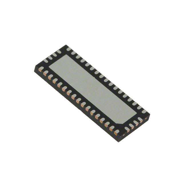
| 描述 | IC MUX/DEMUX 2X1 28TQFN |
| 产品分类 | |
| 品牌 | Pericom |
| 数据手册 | |
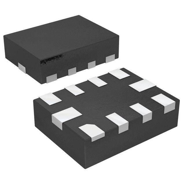
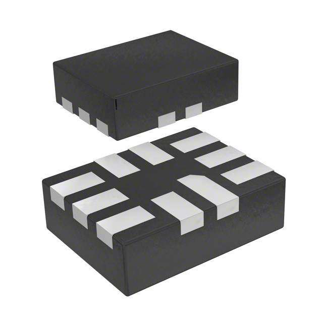
| 产品图片 |
|
| 产品型号 | PI2PCIE2212ZHE |
| rohs | 无铅 / 符合限制有害物质指令(RoHS)规范要求 |
| 产品系列 | - |
| 产品培训模块 | http://www.digikey.cn/PTM/IndividualPTM.page?site=cn&lang=zhs&ptm=26098 |
| 供应商器件封装 | 28-TQFN-EP(3.5x5.5) |
| 功能 | 多路复用器/多路分解器 |
| 包装 | 管件 |
| 安装类型 | 表面贴装 |
| 导通电阻 | - |
| 封装/外壳 | 28-VFQFN 裸露焊盘 |
| 工作温度 | -40°C ~ 85°C |
| 标准包装 | 490 |
| 电压-电源,单/双 (±) | 1.5 V ~ 1.8 V |
| 电压源 | 单电源 |
| 电流-电源 | - |
| 电路 | 2 x 2:1 |


PDF Datasheet 数据手册内容提取
PI2PCIE2212 PCI Express® 2.0, 1-Lane, 2:1 Mux/DeMux Switch w/ Single Enable Features Description • 2 Differential Channel, 2:1 Mux/DeMux Pericom Semiconductor’s PI2PCIE2212 is a 4 to 2 differential, • PCI Express® 2.0 performance, 5.0 Gbps bi-directional channel multiplexer/demultiplexer switch. Due to • Bi-directional operation its low bit-to-bit skew, high channel-to-channel noise isolation • Low Bit-to-Bit Skew, 7ps and bandwidth, this product is ideal for PCI Express® 2.0 signal switching at 5.0Gbps. • Low Crosstalk: -38dB@2.5GHz • Low Off Isolation: -25dB@2.5GHz • VDD Operating Range: 1.5V to 1.8V ±10% Application • ESD Tolerance: 2kV Switch a PCI Express® lane output between two PCI Express lane • Packaging: – 28-contact TQFN (3.5 × 5.5mm) inputs Pin Description (Top-Side View) Block Diagram D D D D A0+ B0+ D N D N V G V G A0- B0- A1+ B1+ 28 27 26 25 A1- B1- GND 1 24 B0+ SEL 2 23 B0- C0+ VDD 3 22 B1+ C0- C1+ AO+ 4 21 B1- C1- AO- 5 20 GND GND SEL A1+ 6 19 VDD A1- 7 18 C0+ V 8 17 C0- DD VDD 9 16 C1+ GND 10 15 C1- Truth Table 11 12 13 14 Function SEL D D D D A to B L VD GN VD GN A to C H 14-0032 1 www.pericom.com 03/26/2014
PI2PCIE2212 PCI Express® 2.0, 1-Lane 2:1 Mux/DeMux Switch w/ Single Enable Maximum Ratings (Above which useful life may be impaired. For user guidelines, not tested.) Storage Temperature .........................................–65°C to +150°C Note: Stresses greater than those listed under MAXIMUM RATINGS may cause permanent damage to the device. This is a stress rating only Supply Voltage to Ground Potential ....................–0.5V to +2.5V and functional operation of the device at these or any other conditions DC Input Voltage .................................................–0.5V to +VDD above those indicated in the operational sections of this specification DC Output Current ...........................................................120mA is not implied. Exposure to absolute maximum rating conditions for Power Dissipation ................................................................0.5W extended periods may affect reliability. Power Supply Characteristics Parameters Description Test Conditions Min. Typ.(1) Max. Units IDD Quiescent Power Supply Current VDD = Max., VIN = GND or VDD 400 µA Notes: 1. Typical values are at VDD = 1.8V, TA = 25°C ambient and maximum loading. DC Electrical Characteristics (TA = –40°C to +85°C, VDD = 1.5V to 1.8V ±10%) Parameter Description Test Conditions Min. Typ.(1) Max. Units VIH Input HIGH Voltage Control Input, SEL Guaranteed HIGH level 0.65 x VDD - - VIL Input LOW Voltage Control Input, SEL Guaranteed LOW level -0.5 - 0.35 x VDD V VIK Clamp Diode Voltage Control Input, SEL VDD = Max., IIN = –18mA - -0.7 -1.2 IIH Input HIGH Current Control Input, SEL VDD = Max., VIN = VDD - - ±5 μA IIL Input LOW Current Control Input, SEL VDD = Max., VIN = GND - - ±5 VO/VI > 95%, RL =10K -0.4 2.4 DC Signal Voltage Range, Channel I/O VIDC (Ax, Bx, Cx) VO/VI > 80%, RL =50- -0.3 2.0 V ohms Notes: 1. Typical values are at VDD = 1.8V, TA = 25°C ambient and maximum loading. (2) Dynamic Electrical Characteristics (TA= -40º to +85ºC, VDD = 1.5V to 1.8V ±10%) Parameter Description Test Conditions Min. Typ.(1) Max. Units XTALK Crosstalk f = 2.5 GHz -38 OIRR OFF Isolation f = 2.5 GHz -25 dB Differential ILOSS f= 2.5 GHz -2.0 Insertion Loss BW Bandwidth -3dB 3.8 Insertion loss 1.5 dB, VIN = 0.6Vpp, DC = 0V 2.5 Max Signal Fre- Insertion loss 1.5 dB, VIN = 0.6Vpp, DC = 0.9V 2.5 GHz VIf quency Range Insertion loss 3.0 dB, VIN = 0.6Vpp, DC = 0V 4.0 Insertion loss 3.0 dB, VIN = 0.6Vpp, DC = 0.9V 4.0 RL = 50, f = 625MHz, Sinewave, DC = 0V 1.2 1 dB Compression P-1dB RL = 50, f = 625MHz, Sinewave, DC = 0.45V 2.0 Vpp Input Signal RL = 50, f = 625MHz, Sinewave, DC = 0.9V 2.4 Notes: 1. Typical values are at VDD = 1.8V, TA = 25°C ambient and maximum loading. 2. Guaranteed by design. 14-0032 2 www.pericom.com 03/26/2014
PI2PCIE2212 PCI Express® 2.0, 1-Lane 2:1 Mux/DeMux Switch w/ Single Enable Switching Characteristics (TA= -40º to +85ºC, VDD = 1.5V to 1.8V ±10%) Paramenter Description Min. Typ.(1) Max. Units tPZH, tPZL Line Enable Time - SEL to AN, BN, CN 0.5 - 8.0 ns tPHZ, tPLZ Line Disable Time - SEL to AN, BN, CN 0.5 - 8.0 tb-b Bit-to-bit skew within the same differential pair 15 ps tch-ch Channel-to-channel skew 20 Note: 1. Typical values are at VDD = 1.8V, TA = 25°C ambient and maximum loading. Test Circuit for Electrical Characteristics(1-5) Switch Positions 2 x VDD Test Switch VDD tPLZ, tPZL 2 x VDD tPHZ, tPZH GND 200-Ohm VIN VOUT Prop Delay Open Pulse D.U.T Generator 4pF RT CL 200-Ohm Notes: 1. CL = Load capacitance: includes jig and probe capacitance. 2. RT = Termination resistance: should be equal to ZOUT of the Pulse Generator 3. Output 1 is for an output with internal conditions such that the output is low except when disabled by the output control. output 2 is for an output with internal conditions such that the output is high except when disabled by the output control. 4. All input impulses are supplied by generators having the following characteristics: PRR ≤ MHz, ZO = 50Ω, tR ≤ 2.5ns, tF ≤ 2.5ns. 5. The outputs are measured one at a time with one transition per measurement. Switching Waveforms SEL VDD V /2 V /2 DD DD 0V tPZL Output tPLZ VOH V DD/2 V +0.3V OL VOL tPZH tPHZ VOH VDD/2 VOH –0.3V Output VOL Voltage Waveforms Enable and Disable Times 14-0032 3 www.pericom.com 03/26/2014
PI2PCIE2212 PCI Express® 2.0, 1-Lane 2:1 Mux/DeMux Switch w/ Single Enable Crosstalk Off Isolation 14-0032 4 www.pericom.com 03/26/2014
PI2PCIE2212 PCI Express® 2.0, 1-Lane 2:1 Mux/DeMux Switch w/ Single Enable Insertion Loss + + 50 + + 50 BALANCED BALANCED + + PORT1 – – 50 PORT1 – – 50 BALANCED BALANCED PORT1 – – PORT2 + + + 50 BALANCED BALANCED DUT – PORT2 PORT2 – – 50 DUT DUT Diff. Insertion Loss and Return Test Diff. Off Isolation Test Circuit Diff. Near End Xtalk Test Circuit Circuit 14-0032 5 www.pericom.com 03/26/2014
PI2PCIE2212 PCI Express® 2.0, 1-Lane 2:1 Mux/DeMux Switch w/ Single Enable Packaging Mechanical: 28-Pin TQFN (ZH) DATE: 07/11/12 DESCRIPTION: 28-Contact, Very Thin Quad Flat No-Lead, TQFN PACKAGE CODE: ZH28 DOCUMENT CONTROL #: PD-2034 REVISION: C 12-0419 Note: • For latest package info, please check: http://www.pericom.com/products/packaging/mechanicals.php Ordering Information Ordering Code Package Code Package Type PI2PCIE2212ZHEX ZH 28-contact, Very Thin Quad Flat No-Lead (TQFN) Notes: • Thermal characteristics can be found on the company web site at www.pericom.com/packaging/ • E = Pb-free and Green • Adding an X suffix = Tape/Reel Pericom Semiconductor Corporation • 1-800-435-2336 • www.pericom.com 14-0032 6 www.pericom.com 03/26/2014 All trademarks are property of their respective owners.
Mouser Electronics Authorized Distributor Click to View Pricing, Inventory, Delivery & Lifecycle Information: D iodes Incorporated: PI2PCIE2212ZHE PI2PCIE2212ZHEX