 Datasheet下载
- 型号: PGA2311U
- 制造商: Texas Instruments
- 库位|库存: xxxx|xxxx
- 要求:
| 数量阶梯 | 香港交货 | 国内含税 |
| +xxxx | $xxxx | ¥xxxx |
查看当月历史价格
查看今年历史价格
PGA2311U产品简介:
ICGOO电子元器件商城为您提供PGA2311U由Texas Instruments设计生产,在icgoo商城现货销售,并且可以通过原厂、代理商等渠道进行代购。 PGA2311U价格参考。Texas InstrumentsPGA2311U封装/规格:音频专用, Audio Volume Control 2 Channel 16-SOIC。您可以下载PGA2311U参考资料、Datasheet数据手册功能说明书,资料中有PGA2311U 详细功能的应用电路图电压和使用方法及教程。
Texas Instruments(德州仪器)的PGA2311U是一款专为音频应用设计的集成数字控制立体声可编程增益放大器。它具有广泛的应用场景,特别是在需要高精度音量调节和信号处理的设备中。以下是PGA2311U的主要应用场景:

1. 消费电子设备:
   - 便携式音频播放器:如MP3播放器、智能手机和平板电脑等,PGA2311U可以提供高质量的音量控制和音频信号增强。
   - 蓝牙音箱和耳机:用于无线音频设备中的音量调节和信号处理,确保用户获得一致且高品质的音频体验。

2. 家庭娱乐系统:
   - AV接收器和音响系统:在家庭影院系统中,PGA2311U可以实现多通道音频信号的精确控制,提升整体音质表现。
   - 智能电视和机顶盒:通过集成PGA2311U,这些设备可以在不同音源之间平滑切换,并保持稳定的音量输出。

3. 专业音频设备:
   - 调音台和混音器:用于广播电台、录音棚和现场演出场合,PGA2311U能够精确调整每个音频通道的增益,确保音频信号的最佳传输。
   - 监听音箱和耳放:在音频制作过程中,PGA2311U可以帮助工程师和音乐人进行精细的音量控制,以实现更准确的音频监听。

4. 汽车音响系统:
   - 车载收音机和多媒体主机:PGA2311U可以优化车内音频系统的性能,提高声音清晰度和动态范围,使驾驶者和乘客享受更好的音乐体验。
   - 后装市场音频升级套件:为已有的车辆添加或升级音频功能时,PGA2311U提供了灵活且高效的解决方案。

5. 工业和医疗设备:
   - 通信设备:如对讲机和其他语音通信装置,PGA2311U能有效提升语音清晰度,确保通信质量。
   - 医疗监护仪:用于心电图机、超声波设备等,PGA2311U可以稳定地处理和放大生物电信号,帮助医生更准确地诊断病情。

总之,PGA2311U凭借其高性能和灵活性,在各类音频设备中发挥着重要作用,满足了从消费级到专业级的不同需求。
| 参数 | 数值 |
| 产品目录 | 集成电路 (IC)半导体 |
| 描述 | IC 5V STEREO AUD VOL CTRL 16SOIC音频放大器 5V Stereo Audio Volume Control |
| 产品分类 | 线性 - 音频处理集成电路 - IC |
| 品牌 | Texas Instruments |
| 产品手册 | http://www.ti.com/litv/sbos218a |
| 产品图片 |
|
| rohs | 符合RoHS无铅 / 符合限制有害物质指令(RoHS)规范要求 |
| 产品系列 | 音频 IC,音频放大器,Texas Instruments PGA2311U- |
| 数据手册 | |
| 产品型号 | PGA2311U |
| THD+噪声 | 0.0002 % |
| 产品 | General Purpose Audio Amplifiers |
| 产品目录页面 | |
| 产品种类 | 音频放大器 |
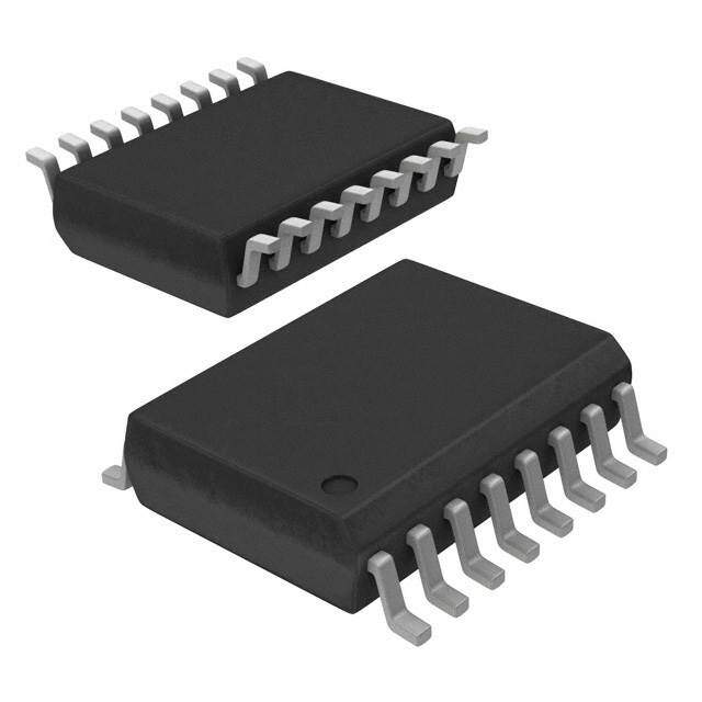
| 供应商器件封装 | 16-SOIC |
| 其它名称 | 296-12458-5 |
| 包装 | 管件 |
| 单位重量 | 420.400 mg |
| 商标 | Texas Instruments |
| 增益 | 31.5 dB |
| 增益带宽生成 | 10 MHz |
| 安装类型 | 表面贴装 |
| 安装风格 | SMD/SMT |
| 封装 | Tube |
| 封装/外壳 | 16-SOIC(0.295",7.50mm 宽) |
| 封装/箱体 | SOIC-16 |
| 工作电源电压 | 5 V |
| 工厂包装数量 | 40 |
| 应用 | 放大器,接收器 |
| 最大工作温度 | + 85 C |
| 最小工作温度 | - 40 C |
| 标准包装 | 40 |
| 电源电压-最大 | 5.25 V |
| 电源电压-最小 | 4.75 V |
| 电源电流 | 8 mA |
| 电源类型 | Single |
| 类型 | 立体声音量控制 |
| 系列 | PGA2311 |
| 输入补偿电压 | 0.25 mV |
| 音频负载电阻 | 10 kOhms |

.jpg)


PDF Datasheet 数据手册内容提取
Product Sample & Technical Tools & Support & Folder Buy Documents Software Community PGA2311 SBOS218D–DECEMBER2001–REVISEDMAY2016 PGA2311 Stereo Audio Volume Control 1 Features 3 Description • Digitally-ControlledAnalogVolumeControl: The PGA2311 device is a high-performance, stereo 1 audio volume control designed for professional and – TwoIndependentAudioChannels high-end consumer audio systems. The PGA2311 – SerialControlInterface uses an internal high-performance operational – ZeroCrossingDetection amplifier to yield low noise and distortion. The PGA2311 also provides the capability to drive 660-Ω – MuteFunction loads directly without buffering. The 3-wire serial • WideGainandAttenuationRange: control interface allows for connection to a wide +31.5dBto−95.5dBwith0.5-dBSteps variety of host controllers, in addition to support for • LowNoiseandDistortion: daisy-chainingofmultiplePGA2311devices. – 120-dBDynamicRange DeviceInformation(1) – 0.0004%THD+Nat1kHz(U-Grade) PARTNUMBER PACKAGE BODYSIZE(NOM) – 0.0002%THD+Nat1kHz(A-Grade) SOIC(16) 7.5mm×10.30mm • Noise-FreeLevelTransitions PGA2311 PDIP(16) 6.35mm×19.30mm • LowInterchannelCrosstalk: −130dBFS (1) For all available packages, see the orderable addendum at • PowerSupplies:±5-VAnalog,+5-VDigital theendofthedatasheet. • AvailableinPDIP-16andSOIC-16Packages • Pin-andSoftware-CompatibleWiththeCrystal CS3310 2 Applications • AudioAmplifiers StereoAudioVolumeControl • MixingConsoles • Multi-TrackRecorders • BroadcastStudioEquipment • MusicalInstruments • EffectsProcessors • A/VReceivers • CarAudioSystems Copyright © 2016,Texas Instruments Incorporated 1 An IMPORTANT NOTICE at the end of this data sheet addresses availability, warranty, changes, use in safety-critical applications, intellectualpropertymattersandotherimportantdisclaimers.PRODUCTIONDATA.
PGA2311 SBOS218D–DECEMBER2001–REVISEDMAY2016 www.ti.com Table of Contents 1 Features.................................................................. 1 7.4 DeviceFunctionalModes........................................12 2 Applications........................................................... 1 7.5 Programming..........................................................12 3 Description............................................................. 1 8 ApplicationandImplementation........................ 13 4 RevisionHistory..................................................... 2 8.1 ApplicationInformation............................................13 8.2 TypicalApplication .................................................13 5 PinConfigurationandFunctions......................... 3 9 PowerSupplyRecommendations...................... 14 6 Specifications......................................................... 4 10 Layout................................................................... 15 6.1 AbsoluteMaximumRatings......................................4 6.2 ESDRatings..............................................................4 10.1 LayoutGuidelines.................................................15 6.3 RecommendedOperatingConditions.......................4 10.2 LayoutExample....................................................15 6.4 ThermalInformation..................................................4 11 DeviceandDocumentationSupport................. 16 6.5 ElectricalCharacteristics...........................................5 11.1 DocumentationSupport .......................................16 6.6 TypicalCharacteristics..............................................8 11.2 CommunityResources..........................................16 7 DetailedDescription............................................ 10 11.3 Trademarks...........................................................16 7.1 Overview.................................................................10 11.4 ElectrostaticDischargeCaution............................16 7.2 FunctionalBlockDiagram.......................................10 11.5 Glossary................................................................16 7.3 FeatureDescription.................................................10 12 Mechanical,Packaging,andOrderable Information........................................................... 16 4 Revision History NOTE:Pagenumbersforpreviousrevisionsmaydifferfrompagenumbersinthecurrentversion. ChangesfromRevisionC(May2016)toRevisionD Page • ChangedthevaluesofVoltagerange,PGA2311PA,UA(A−grade)To:(V -)=+1.25V,and(V -)=–1.25Vinthe A A ElectricalCharacteristicstable............................................................................................................................................... 5 • ChnagedtheQuiescentcurrentTestConditionsTo:V =+5V,andV =–5VintheElectricalCharacteristicstable .......6 A A ChangesfromRevisionB(January2016)toRevisionC Page • ChangedpackagefamilytermsinsecondtolastFeaturesbullet ......................................................................................... 1 • Changeddescriptionofpin7inPinFunctionstable ............................................................................................................. 3 • DeletedleadtemperatureandpackagetemperaturerowsfromAbsoluteMaximumRatingstable...................................... 4 ChangesfromRevisionA(June2002)toRevisionB Page • AddedESDRatingstable,FeatureDescriptionsection,DeviceFunctionalModes,ApplicationandImplementation section,PowerSupplyRecommendationssection,Layoutsection,DeviceandDocumentationSupportsection,and Mechanical,Packaging,andOrderableInformationsection. ................................................................................................ 1 2 SubmitDocumentationFeedback Copyright©2001–2016,TexasInstrumentsIncorporated ProductFolderLinks:PGA2311
PGA2311 www.ti.com SBOS218D–DECEMBER2001–REVISEDMAY2016 5 Pin Configuration and Functions NorDWPackage 16-PinPDIPorSOIC TopView PinFunctions PIN I/O DESCRIPTION NO. NAME 1 ZCEN I Zero-crossingenableinput(activehigh) 2 CS I Chip-selectinput(activelow) 3 SDI I Serialdatainput 4 V + I Digitalpowersupply,+5V D 5 DGND — Digitalground 6 SCLK I Serialclockinput 7 SDO O Serialdataoutput 8 MUTE I Mutecontrolinput(activelow) 9 V R I Analoginput,rightchannel IN 10 AGNDR — Analogground,rightchannel 11 V R O Analogoutput,rightchannel OUT 12 V + I Analogpowersupply,+5V A 13 V – I Analogpowersupply,–5V A 14 V L O Analogoutput,leftchannel OUT 15 AGNDL — Analogground,leftchannel 16 V L I Analoginput,leftchannel IN Copyright©2001–2016,TexasInstrumentsIncorporated SubmitDocumentationFeedback 3 ProductFolderLinks:PGA2311
PGA2311 SBOS218D–DECEMBER2001–REVISEDMAY2016 www.ti.com 6 Specifications 6.1 Absolute Maximum Ratings overoperatingfree-airtemperaturerange(unlessotherwisenoted)(1) MIN MAX UNIT V + 5.5 A V – –5.5 A Supplyvoltage V V + 5.5 D V +toV + <±0.3 A D Analoginputvoltage 0 V +,V − V A A Digitalinputvoltage –0.3 V + V D Operatingtemperature –40 85 °C Junctiontemperature 150 °C Storagetemperature,T –65 150 °C stg (1) StressesbeyondthoselistedunderAbsoluteMaximumRatingsmaycausepermanentdamagetothedevice.Thesearestressratings only,whichdonotimplyfunctionaloperationofthedeviceattheseoranyotherconditionsbeyondthoseindicatedunderRecommended OperatingConditions.Exposuretoabsolute-maximum-ratedconditionsforextendedperiodsmayaffectdevicereliability. 6.2 ESD Ratings VALUE UNIT PGA2311in16-PinSOICPackage Human-bodymodel(HBM),perANSI/ESDA/JEDECJS-001(1) ±2000 V Electrostaticdischarge V (ESD) Charged-devicemodel(CDM),perJEDECspecificationJESD22-C101(2) ±1500 PGA2311in16-PinPDIPPackage V Electrostaticdischarge Human-bodymodel(HBM),perANSI/ESDA/JEDECJS-001(1) ±2000 V (ESD) (1) JEDECdocumentJEP155statesthat500-VHBMallowssafemanufacturingwithastandardESDcontrolprocess. (2) JEDECdocumentJEP157statesthat250-VCDMallowssafemanufacturingwithastandardESDcontrolprocess. 6.3 Recommended Operating Conditions overoperatingfree-airtemperaturerange(unlessotherwisenoted) MIN NOM MAX UNIT V + Positiveanalogpowersupply 4.75 5 5.25 V A V – Negativeanalogpowersupply –4.75 –5 –5.25 V A V + Digitalpowersupply 4.75 5 5.25 V D Operatingtemperature –40 25 85 °C 6.4 Thermal Information PGA2311 THERMALMETRIC(1) N(PDIP) DW(SOIC) UNIT 16PINS 16PINS R Junction-to-ambientthermalresistance 39.9 83 °C/W θJA R Junction-to-case(top)thermalresistance 26.2 44 °C/W θJC(top) R Junction-to-boardthermalresistance 20.1 40.5 °C/W θJB ψ Junction-to-topcharacterizationparameter 10.7 11.5 °C/W JT ψ Junction-to-boardcharacterizationparameter 19.9 40.2 °C/W JB R Junction-to-case(bottom)thermalresistance — — °C/W θJC(bot) (1) Formoreinformationabouttraditionalandnewthermalmetrics,seetheSemiconductorandICPackageThermalMetricsapplication report,SPRA953. 4 SubmitDocumentationFeedback Copyright©2001–2016,TexasInstrumentsIncorporated ProductFolderLinks:PGA2311
PGA2311 www.ti.com SBOS218D–DECEMBER2001–REVISEDMAY2016 6.5 Electrical Characteristics AtT =+25°C,V +=+5V,V −=–5V,V +=+5V,R =100kΩ,C =20pF,BWmeasure=10Hzto20kHz,unless A A A D L L otherwisenoted. PARAMETER TESTCONDITIONS MIN TYP MAX UNIT DCCHARACTERISTICS Stepsize 0.5 dB Gainerror Gainsetting=31.5dB ±0.05 dB Gainmatching ±0.05 dB Inputresistance 10 kΩ PGA2311P,U(U−grade) 3 Inputcapacitance pF PGA2311PA,UA(A−grade) 7 ACCHARACTERISTICS PGA2311P, 0.0004% 0.001% V =2Vrms, U(U−grade) THD+N IN f=1kHz PGA2311PA, 0.0002% 0.0004% UA(A−grade) Dynamicrange V =AGND,gain=0dB 116 120 dB IN PGA2311P,U(U−grade) (V −)+1.25 (V +)–1.25 A A Voltagerange,output V PGA2311PA,UA(A−grade) (V −)+1.25 (V −)−1.25 A A Voltagerange,input 2.5 Vrms (withoutclipping) Outputnoise V =AGND,gain=0dB 2.5 4 μV IN RMS Interchannelcrosstalk f=1kHz –130 dBFS OUTPUTBUFFER Offsetvoltage V =AGND,gain=0dB 0.25 0.5 mV IN Loadcapacitancestability 100 pF Short-circuitcurrent 50 mA Unity-gainbandwidth,smallsignal 10 MHz DIGITALCHARACTERISTICS V High-levelinputvoltage 2 V + V IH D V Low-levelinputvoltage –0.3 0.8 V IL PGA2311P, (V +)−1 U(U−grade) A V High-leveloutputvoltage I =200μA V OH O PGA2311PA, (V +)−1 UA(A−grade) D V Low-leveloutputvoltage I =–3.2mA 0.4 V OL O Inputleakagecurrent 1 10 µA SWITCHINGCHARACTERISTICS f Serialclock(SCLK)frequency 0 6.25 MHz SCLK t SCLKpulsedurationlow 80 ns PL t SCLKpulsedurationhigh 80 ns PH t MUTEpulsedurationlow 2 ms MI INPUTTIMING t SDIsetuptime 20 ns SDS t SDIholdtime 20 ns SDH t CSfallingtoSCLKrising 90 ns CSCR t SCLKfallingtoCSrising 35 ns CFCS OUTPUTTIMING t CSlowtoSDOactive 35 ns CSO t SCLKfallingtoSDOdatavalid 60 ns CFDO t CShightoSDOhighimpedance 100 ns CSZ Copyright©2001–2016,TexasInstrumentsIncorporated SubmitDocumentationFeedback 5 ProductFolderLinks:PGA2311
PGA2311 SBOS218D–DECEMBER2001–REVISEDMAY2016 www.ti.com Electrical Characteristics (continued) AtT =+25°C,V +=+5V,V −=–5V,V +=+5V,R =100kΩ,C =20pF,BWmeasure=10Hzto20kHz,unless A A A D L L otherwisenoted. PARAMETER TESTCONDITIONS MIN TYP MAX UNIT POWERSUPPLY V + 4.75 5 5.25 A Operatingvoltage V – –4.75 –5 –5.25 V A V + 4.75 5 5.25 D I + V +=+5V 8 10 A A Quiescentcurrent I – V –=–5V 10 12 mA A A I + V +=+5V 0.5 1 D D Power-supplyrejectionratio PSRR 100 dB (250Hz) TEMPERATURERANGE Operatingrange –40 85 °C GainByteFormatisMSBFirst,StraightBinary R0 is the Least Significant Bit of the Right Channel Gain Byte R7 is the Most Significant Bit of the Right Channel Gain Byte L0 is the Least Significant Bit of the Left Channel Gain Byte L7 is the Most Significant Bit of the Left Channel Gain Byte SDI is latched on the rising edge of SCLK. SDO transitions on the falling edge of SCLK. Figure1. SerialInterfaceProtocol 6 SubmitDocumentationFeedback Copyright©2001–2016,TexasInstrumentsIncorporated ProductFolderLinks:PGA2311
PGA2311 www.ti.com SBOS218D–DECEMBER2001–REVISEDMAY2016 Figure2. SerialInterfaceTimingRequirements Copyright©2001–2016,TexasInstrumentsIncorporated SubmitDocumentationFeedback 7 ProductFolderLinks:PGA2311
PGA2311 SBOS218D–DECEMBER2001–REVISEDMAY2016 www.ti.com 6.6 Typical Characteristics AtT =+25°C,V +=+5V,V −=−5V,V +=+5V,R =100kΩ,C =20pF,BWmeasure=10Hzto20kHz,unless A A A D L L otherwisenoted.AllplotstakenwithPGA2311A-grade. Gain=0dB,Load=100kΩ,VIN=2Vrms Gain=0dB,Freq=1kHz,Load=100kΩ Figure3.AmplitudevsFrequency Figure4.THD+NvsAmplitude Gain=0dB,Freq=1kHz,Load=600Ω Gain=0dB,V =2Vrms,Load=100kΩ IN Figure5.THD+NvsAmplitude Figure6.THD+NvsFrequency Gain=0dB,VIN=2Vrms,Load=600Ω Gain=0dB,VIN=2Vrms,FIN=1kHz Figure7.THD+NvsFrequency Figure8.THD+NvsInputSourceImpedance 8 SubmitDocumentationFeedback Copyright©2001–2016,TexasInstrumentsIncorporated ProductFolderLinks:PGA2311
PGA2311 www.ti.com SBOS218D–DECEMBER2001–REVISEDMAY2016 Typical Characteristics (continued) AtT =+25°C,V +=+5V,V −=−5V,V +=+5V,R =100kΩ,C =20pF,BWmeasure=10Hzto20kHz,unless A A A D L L otherwisenoted.AllplotstakenwithPGA2311A-grade. Figure9.CrosstalkWithF =1kHz Figure10.CrosstalkWithF =10kHz IN IN Figure11.CrosstalkWithF =20kHz IN Copyright©2001–2016,TexasInstrumentsIncorporated SubmitDocumentationFeedback 9 ProductFolderLinks:PGA2311
PGA2311 SBOS218D–DECEMBER2001–REVISEDMAY2016 www.ti.com 7 Detailed Description 7.1 Overview The PGA2311 is a stereo audio volume control that can be used in a wide array of professional and consumer audioequipment.ThePGA2311isfabricatedinasub-micronCMOSprocess. The heart of the PGA2311 is a resistor network, an analog switch array, and a high-performance operational amplifier stage. The switches select taps in the resistor network that determine the gain of the amplifier stage. Switch selections are programmed using a serial control port. The serial port allows connection to a wide variety ofhostcontrollers.TheFunctionalBlockDiagramsectionshowsamodeldiagramofthePGA2311. 7.2 Functional Block Diagram Copyright © 2016,Texas Instruments Incorporated 7.3 Feature Description 7.3.1 AnalogInputsandOutputs The PGA2311 includes two independent channels (referred to as the left and right channels). Each channel has a corresponding input and output pin. The input and output pins are unbalanced, or referenced to analog ground (either AGNDR or AGNDL). The inputs are V R (pin 9) and V L (pin 16), and the outputs are V R (pin 11) IN IN OUT andV L(pin14).Theinputandoutputpinscanswingwithin1.25Voftheanalogpowersupplies,V +(pin12) OUT A andV −(pin13).GivenV +=+5VandV −= −5V,themaximuminputoroutputvoltagerangeis7.5Vp-p. A A A Foroptimalperformance,drivethePGA2311withalowsourceimpedance.Asourceimpedanceof600 Ω orless is recommended. Source impedances up to 2 kΩ cause minimal degradation of THD+N; see Figure 8 for more details. 10 SubmitDocumentationFeedback Copyright©2001–2016,TexasInstrumentsIncorporated ProductFolderLinks:PGA2311
PGA2311 www.ti.com SBOS218D–DECEMBER2001–REVISEDMAY2016 Feature Description (continued) 7.3.2 GainSettings The gain for each channel is set by its corresponding 8-bit code, either R[7:0] or L[7:0] (see Figure 1). The gain code data is straight binary format. If N equals the decimal equivalent of R[7:0] or L[7:0], then the following relationshipsexistforthegainsettings: • ForN=0:MuteCondition.Theinputmultiplexerisconnectedtoanalogground(AGNDRorAGNDL). • ForN=1to255:Gain(dB)=31.5 −[0.5w(255 − N)] Thisresultsinagainrangeof+31.5dB(withN=255)to −95.5dB(withN=1). Changes in gain setting can be made with or without zero-crossing detection. The operation of the zero-crossing detectorandtimeoutcircuitryisdiscussedintheZero-CrossingDetection section. 7.3.3 Daisy-ChainingMultiplePGA2311Devices To reduce the number of control signals required to support multiple PGA2311 devices on a printed circuit board (PCB), the serial control port supports daisy-chaining of multiple PGA2311 devices. Figure 12 shows the connection requirements for daisy-chain operation. This arrangement allows a 3-wire serial interface to control manyPGA2311devices. As shown in Figure 12, the SDO pin from PGA2311 #1 is connected to the SDI input of PGA2311 #2, and is repeated for additional devices. This configuration in turn forms a large shift register, in which gain data can be written for all PGA2311s connected to the serial bus. The length of the shift register is 16 × N bits, where N is equal to the number of PGA2311 devices included in the chain. The CS input must remain LOW for 16 × N SCLKperiods,whereNisthenumberofdevicesconnectedinthechain,toallowenoughSCLKcyclestoloadall devices. Figure12. Daisy-ChainingMultiplePGA2311Devices Copyright©2001–2016,TexasInstrumentsIncorporated SubmitDocumentationFeedback 11 ProductFolderLinks:PGA2311
PGA2311 SBOS218D–DECEMBER2001–REVISEDMAY2016 www.ti.com Feature Description (continued) 7.3.4 Zero-CrossingDetection The PGA2311 includes a zero-crossing detection function for noise-free level transitions. The concept is to change gain settings on a zero-crossing of the input signal, thus minimizing audible glitches. This function is enabled or disabled using the ZCEN input (pin 1). When ZCEN is LOW, zero-crossing detection is disabled. WhenZCENisHIGH,zero-crossingdetectionisenabled. Thezero-crossingdetectiontakeseffectwithachangeingainsettingforacorrespondingchannel.Thenewgain setting is not implemented until either a positive slope zero crossing is detected, or a time-out period of 16 ms has elapsed. In the case of a time-out, the new gain setting takes effect with no attempt to minimize audible artifacts. 7.3.5 MUTEFunction Muting can be achieved by either hardware or software control. Hardware muting is accomplished through the MUTEinput,andsoftwaremutingbyloadingallzeroesintothevolumecontrolregister. MUTE disconnects the internal buffer amplifiers from the output pins and terminates A L and A R with OUT OUT 10-kΩ resistors to ground. The mute is activated with a zero-crossing detection (independent of the zero-cross enable status), or an 16-ms time-out to eliminate any audible clicks or pops. MUTE also initiates an internal offsetcalibration. A software mute is implemented by loading all zeroes into the volume control register. The internal amplifier is settounitygain,withtheamplifierinputconnectedtoAGND. 7.4 Device Functional Modes 7.4.1 Power-UpState On power-up, power-up reset is activated for approximately 100 ms, during which the circuit is in hardware MUTE state and all internal flip-flops are reset. At the end of this period, the offset calibration is initiated without any external signals. When this step is complete, the gain byte value for both the left and right channels are set to 00 , or the software MUTE condition. The gain remains at this setting until the host controller programs new HEX settingsforeachchannelviatheserialcontrolport. If the power-supply voltage drops below ±3.2 V during normal operation, the circuit enters a hardware MUTE state.Apower-upsequenceinitiatesifthepower-supplyvoltagereturnstogreaterthan ±3.2V. 7.5 Programming The serial control port is used to program the gain settings for the PGA2311. The serial control port includes threeinputpinsandoneoutputpin.TheinputsincludeCS(pin2),SDI(pin3),andSCLK(pin6).Thesoleoutput pinisSDO(pin7). The CS pin functions as the chip-select input. Data can be written to the PGA2311 only when CS is LOW. SDI is the serial data input pin. Control data are provided as a 16-bit word at the SDI pin, 8 bits each for the left and rightchannelgainsettings. Data are formatted as MSB first, in straight binary code. SCLK is the serial clock input. Data are clocked into SDI ontherisingedgeofSCLK. SDO is the serial data output pin, and used when daisy-chaining multiple PGA2311 devices. Daisy-chain operation is described in the Daisy-Chaining Multiple PGA2311 Devices section. SDO is a tri-state output, and assumesahigh-impedancestatewhenCSisHIGH. The protocol for the serial control port is illustrated in Figure 1; see Figure 2 for detailed timing specifications for theserialcontrolport. 12 SubmitDocumentationFeedback Copyright©2001–2016,TexasInstrumentsIncorporated ProductFolderLinks:PGA2311
PGA2311 www.ti.com SBOS218D–DECEMBER2001–REVISEDMAY2016 8 Application and Implementation NOTE Information in the following applications sections is not part of the TI component specification, and TI does not warrant its accuracy or completeness. TI’s customers are responsible for determining suitability of components for their purposes. Customers should validateandtesttheirdesignimplementationtoconfirmsystemfunctionality. 8.1 Application Information The PGA2311 is commonly used as a digitally-controlled analog volume control. Analog volume is controlled throughaserialinterfacein0.5-dBsteps,rangingfromagainof+31.5dBdowntoanattenuationof −95.5dB. 8.2 Typical Application Figure 13 shows the recommended connections for the PGA2311. Place power-supply bypass capacitors as closetothePGA2311packageasphysicallypossible. Copyright © 2016,Texas Instruments Incorporated Figure13. RecommendedConnectionDiagram 8.2.1 DesignRequirements • Widedynamicrange,+35.5dBto –95.5dB • Operatefroma5-Vdigitalsupplyand±5-Vanalogsupplies • Digitally-controlledanalogvolume 8.2.2 DetailedDesignProcedure ThePGA2311isacompletedigitally-controlledanalogstereovolumecontrollersystemonachiprequiringonlya controller to select the gain or attenuation through a serial interface. Figure 13 shows the basic connections to thePGA2311.Placepower-supplybypasscapacitorsasclosetothePGA2311packageasphysicallypossible. Copyright©2001–2016,TexasInstrumentsIncorporated SubmitDocumentationFeedback 13 ProductFolderLinks:PGA2311
PGA2311 SBOS218D–DECEMBER2001–REVISEDMAY2016 www.ti.com Typical Application (continued) 8.2.3 ApplicationCurve 3 0 dB -6 dB -12 dB 1.5 V) ge ( 0 a olt V -1.5 -3 0 0.0004 0.0008 0.0012 0.0016 0.002 Time (s) Figure14.PGA2311Operatingat0dB, –6dBand–12dB 9 Power Supply Recommendations The PGA2311 is specified for operation with its analog power supplies ranging from ±4.75 V to ±5.25 V and its digital power supply ranging from 4.75 V to 5.25 V. Place power-supply bypass capacitors as close to the PGA2311packageasphysicallypossible. 14 SubmitDocumentationFeedback Copyright©2001–2016,TexasInstrumentsIncorporated ProductFolderLinks:PGA2311
PGA2311 www.ti.com SBOS218D–DECEMBER2001–REVISEDMAY2016 10 Layout 10.1 Layout Guidelines The ground planes for the digital and analog sections of the PCB must be separate from one another. The planesmustbeconnectedatasinglepoint.Figure15showstherecommendedPCBfloorplanforthePGA2311. The PGA2311 is mounted so that the device straddles the split between the digital and analog ground planes. Pins 1 through 8 are oriented to the digital side of the board and pins 9 through 16 are on the analog side of the board. 10.2 Layout Example Figure15. TypicalPCBLayoutFloorPlan Copyright©2001–2016,TexasInstrumentsIncorporated SubmitDocumentationFeedback 15 ProductFolderLinks:PGA2311
PGA2311 SBOS218D–DECEMBER2001–REVISEDMAY2016 www.ti.com 11 Device and Documentation Support 11.1 Documentation Support 11.1.1 RelatedDocumentation Forrelateddocumentation,seethefollowing: • CircuitBoardLayoutTechniques,SLOA089 • Shelf-LifeEvaluationofLead-FreeComponentFinishes,SZZA046 11.2 Community Resources The following links connect to TI community resources. Linked contents are provided "AS IS" by the respective contributors. They do not constitute TI specifications and do not necessarily reflect TI's views; see TI's Terms of Use. TIE2E™OnlineCommunity TI'sEngineer-to-Engineer(E2E)Community.Createdtofostercollaboration amongengineers.Ate2e.ti.com,youcanaskquestions,shareknowledge,exploreideasandhelp solveproblemswithfellowengineers. E2EAudioAmplifierForum TI'sEngineer-to-Engineer(E2E)CommunityforAudioAmplifiers.Createdto fostercollaborationamongengineers.Askquestionsandreceiveanswersinreal-time. 11.3 Trademarks E2EisatrademarkofTexasInstruments. Allothertrademarksarethepropertyoftheirrespectiveowners. 11.4 Electrostatic Discharge Caution This integrated circuit can be damaged by ESD. Texas Instruments recommends that all integrated circuits be handled with appropriateprecautions.Failuretoobserveproperhandlingandinstallationprocedurescancausedamage. ESDdamagecanrangefromsubtleperformancedegradationtocompletedevicefailure.Precisionintegratedcircuitsmaybemore susceptibletodamagebecauseverysmallparametricchangescouldcausethedevicenottomeetitspublishedspecifications. 11.5 Glossary SLYZ022—TIGlossary. Thisglossarylistsandexplainsterms,acronyms,anddefinitions. 12 Mechanical, Packaging, and Orderable Information The following pages include mechanical, packaging, and orderable information. This information is the most current data available for the designated devices. This data is subject to change without notice and revision of thisdocument.Forbrowser-basedversionsofthisdatasheet,refertotheleft-handnavigation. 16 SubmitDocumentationFeedback Copyright©2001–2016,TexasInstrumentsIncorporated ProductFolderLinks:PGA2311
PACKAGE OPTION ADDENDUM www.ti.com 6-Feb-2020 PACKAGING INFORMATION Orderable Device Status Package Type Package Pins Package Eco Plan Lead/Ball Finish MSL Peak Temp Op Temp (°C) Device Marking Samples (1) Drawing Qty (2) (6) (3) (4/5) PGA2311P ACTIVE PDIP N 16 25 Green (RoHS NIPDAU N / A for Pkg Type PGA2311P & no Sb/Br) PGA2311PA ACTIVE PDIP N 16 25 Green (RoHS NIPDAU N / A for Pkg Type PGA2311P & no Sb/Br) A PGA2311U ACTIVE SOIC DW 16 40 Green (RoHS NIPDAU Level-2-260C-1 YEAR -40 to 85 PGA2311U & no Sb/Br) PGA2311U/1K ACTIVE SOIC DW 16 1000 Green (RoHS NIPDAU Level-2-260C-1 YEAR -40 to 85 PGA2311U & no Sb/Br) PGA2311U/1KG4 ACTIVE SOIC DW 16 1000 Green (RoHS NIPDAU Level-2-260C-1 YEAR -40 to 85 PGA2311U & no Sb/Br) PGA2311UA ACTIVE SOIC DW 16 40 Green (RoHS NIPDAU Level-2-260C-1 YEAR PGA2311U & no Sb/Br) A PGA2311UA/1K ACTIVE SOIC DW 16 1000 Green (RoHS NIPDAU Level-2-260C-1 YEAR PGA2311U & no Sb/Br) A (1) The marketing status values are defined as follows: ACTIVE: Product device recommended for new designs. LIFEBUY: TI has announced that the device will be discontinued, and a lifetime-buy period is in effect. NRND: Not recommended for new designs. Device is in production to support existing customers, but TI does not recommend using this part in a new design. PREVIEW: Device has been announced but is not in production. Samples may or may not be available. OBSOLETE: TI has discontinued the production of the device. (2) RoHS: TI defines "RoHS" to mean semiconductor products that are compliant with the current EU RoHS requirements for all 10 RoHS substances, including the requirement that RoHS substance do not exceed 0.1% by weight in homogeneous materials. Where designed to be soldered at high temperatures, "RoHS" products are suitable for use in specified lead-free processes. TI may reference these types of products as "Pb-Free". RoHS Exempt: TI defines "RoHS Exempt" to mean products that contain lead but are compliant with EU RoHS pursuant to a specific EU RoHS exemption. Green: TI defines "Green" to mean the content of Chlorine (Cl) and Bromine (Br) based flame retardants meet JS709B low halogen requirements of <=1000ppm threshold. Antimony trioxide based flame retardants must also meet the <=1000ppm threshold requirement. (3) MSL, Peak Temp. - The Moisture Sensitivity Level rating according to the JEDEC industry standard classifications, and peak solder temperature. (4) There may be additional marking, which relates to the logo, the lot trace code information, or the environmental category on the device. (5) Multiple Device Markings will be inside parentheses. Only one Device Marking contained in parentheses and separated by a "~" will appear on a device. If a line is indented then it is a continuation of the previous line and the two combined represent the entire Device Marking for that device. Addendum-Page 1
PACKAGE OPTION ADDENDUM www.ti.com 6-Feb-2020 (6) Lead/Ball Finish - Orderable Devices may have multiple material finish options. Finish options are separated by a vertical ruled line. Lead/Ball Finish values may wrap to two lines if the finish value exceeds the maximum column width. Important Information and Disclaimer:The information provided on this page represents TI's knowledge and belief as of the date that it is provided. TI bases its knowledge and belief on information provided by third parties, and makes no representation or warranty as to the accuracy of such information. Efforts are underway to better integrate information from third parties. TI has taken and continues to take reasonable steps to provide representative and accurate information but may not have conducted destructive testing or chemical analysis on incoming materials and chemicals. TI and TI suppliers consider certain information to be proprietary, and thus CAS numbers and other limited information may not be available for release. In no event shall TI's liability arising out of such information exceed the total purchase price of the TI part(s) at issue in this document sold by TI to Customer on an annual basis. Addendum-Page 2
PACKAGE MATERIALS INFORMATION www.ti.com 27-May-2016 TAPE AND REEL INFORMATION *Alldimensionsarenominal Device Package Package Pins SPQ Reel Reel A0 B0 K0 P1 W Pin1 Type Drawing Diameter Width (mm) (mm) (mm) (mm) (mm) Quadrant (mm) W1(mm) PGA2311U/1K SOIC DW 16 1000 330.0 16.4 10.75 10.7 2.7 12.0 16.0 Q1 PGA2311UA/1K SOIC DW 16 1000 330.0 16.4 10.75 10.7 2.7 12.0 16.0 Q1 PackMaterials-Page1
PACKAGE MATERIALS INFORMATION www.ti.com 27-May-2016 *Alldimensionsarenominal Device PackageType PackageDrawing Pins SPQ Length(mm) Width(mm) Height(mm) PGA2311U/1K SOIC DW 16 1000 367.0 367.0 38.0 PGA2311UA/1K SOIC DW 16 1000 367.0 367.0 38.0 PackMaterials-Page2
None
GENERIC PACKAGE VIEW DW 16 SOIC - 2.65 mm max height 7.5 x 10.3, 1.27 mm pitch SMALL OUTLINE INTEGRATED CIRCUIT This image is a representation of the package family, actual package may vary. Refer to the product data sheet for package details. 4224780/A www.ti.com
PACKAGE OUTLINE DW0016A SOIC - 2.65 mm max height SCALE 1.500 SOIC C 10.63 SEATING PLANE TYP 9.97 A PIN 1 ID 0.1 C AREA 14X 1.27 16 1 10.5 2X 10.1 8.89 NOTE 3 8 9 0.51 16X 0.31 7.6 B 7.4 0.25 C A B 2.65 MAX NOTE 4 0.33 TYP 0.10 SEE DETAIL A 0.25 GAGE PLANE 0.3 0 - 8 0.1 1.27 0.40 DETAIL A (1.4) TYPICAL 4220721/A 07/2016 NOTES: 1. All linear dimensions are in millimeters. Dimensions in parenthesis are for reference only. Dimensioning and tolerancing per ASME Y14.5M. 2. This drawing is subject to change without notice. 3. This dimension does not include mold flash, protrusions, or gate burrs. Mold flash, protrusions, or gate burrs shall not exceed 0.15 mm, per side. 4. This dimension does not include interlead flash. Interlead flash shall not exceed 0.25 mm, per side. 5. Reference JEDEC registration MS-013. www.ti.com
EXAMPLE BOARD LAYOUT DW0016A SOIC - 2.65 mm max height SOIC 16X (2) SEE SYMM DETAILS 1 16 16X (0.6) SYMM 14X (1.27) 8 9 R0.05 TYP (9.3) LAND PATTERN EXAMPLE SCALE:7X METAL SOLDER MASK SOLDER MASK METAL OPENING OPENING 0.07 MAX 0.07 MIN ALL AROUND ALL AROUND NON SOLDER MASK SOLDER MASK DEFINED DEFINED SOLDER MASK DETAILS 4220721/A 07/2016 NOTES: (continued) 6. Publication IPC-7351 may have alternate designs. 7. Solder mask tolerances between and around signal pads can vary based on board fabrication site. www.ti.com
EXAMPLE STENCIL DESIGN DW0016A SOIC - 2.65 mm max height SOIC 16X (2) SYMM 1 16 16X (0.6) SYMM 14X (1.27) 8 9 R0.05 TYP (9.3) SOLDER PASTE EXAMPLE BASED ON 0.125 mm THICK STENCIL SCALE:7X 4220721/A 07/2016 NOTES: (continued) 8. Laser cutting apertures with trapezoidal walls and rounded corners may offer better paste release. IPC-7525 may have alternate design recommendations. 9. Board assembly site may have different recommendations for stencil design. www.ti.com
IMPORTANTNOTICEANDDISCLAIMER TI PROVIDES TECHNICAL AND RELIABILITY DATA (INCLUDING DATASHEETS), DESIGN RESOURCES (INCLUDING REFERENCE DESIGNS), APPLICATION OR OTHER DESIGN ADVICE, WEB TOOLS, SAFETY INFORMATION, AND OTHER RESOURCES “AS IS” AND WITH ALL FAULTS, AND DISCLAIMS ALL WARRANTIES, EXPRESS AND IMPLIED, INCLUDING WITHOUT LIMITATION ANY IMPLIED WARRANTIES OF MERCHANTABILITY, FITNESS FOR A PARTICULAR PURPOSE OR NON-INFRINGEMENT OF THIRD PARTY INTELLECTUAL PROPERTY RIGHTS. These resources are intended for skilled developers designing with TI products. You are solely responsible for (1) selecting the appropriate TI products for your application, (2) designing, validating and testing your application, and (3) ensuring your application meets applicable standards, and any other safety, security, or other requirements. These resources are subject to change without notice. TI grants you permission to use these resources only for development of an application that uses the TI products described in the resource. Other reproduction and display of these resources is prohibited. No license is granted to any other TI intellectual property right or to any third party intellectual property right. TI disclaims responsibility for, and you will fully indemnify TI and its representatives against, any claims, damages, costs, losses, and liabilities arising out of your use of these resources. TI’s products are provided subject to TI’s Terms of Sale (www.ti.com/legal/termsofsale.html) or other applicable terms available either on ti.com or provided in conjunction with such TI products. TI’s provision of these resources does not expand or otherwise alter TI’s applicable warranties or warranty disclaimers for TI products. Mailing Address: Texas Instruments, Post Office Box 655303, Dallas, Texas 75265 Copyright © 2020, Texas Instruments Incorporated