 Datasheet下载
- 型号: PESD3V3L5UF,115
- 制造商: NXP Semiconductors
- 库位|库存: xxxx|xxxx
- 要求:
| 数量阶梯 | 香港交货 | 国内含税 |
| +xxxx | $xxxx | ¥xxxx |
查看当月历史价格
查看今年历史价格
PESD3V3L5UF,115产品简介:
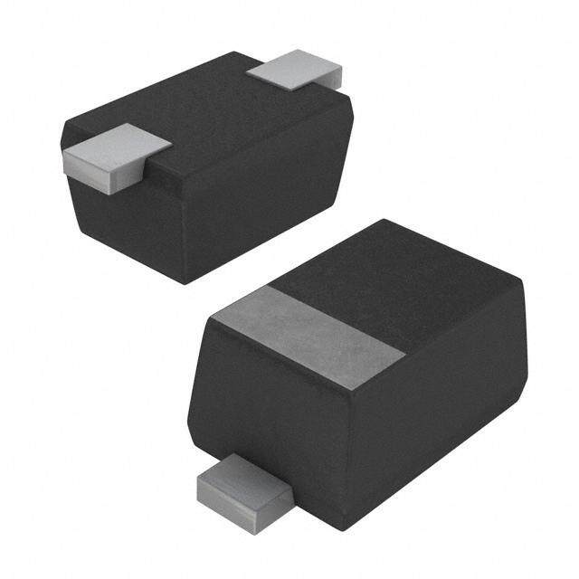
ICGOO电子元器件商城为您提供PESD3V3L5UF,115由NXP Semiconductors设计生产,在icgoo商城现货销售,并且可以通过原厂、代理商等渠道进行代购。 PESD3V3L5UF,115价格参考¥0.84-¥0.84。NXP SemiconductorsPESD3V3L5UF,115封装/规格:TVS - 二极管, 12V Clamp 2.5A (8/20µs) Ipp Tvs Diode Surface Mount 6-XSON, SOT886 (1.45x1)。您可以下载PESD3V3L5UF,115参考资料、Datasheet数据手册功能说明书,资料中有PESD3V3L5UF,115 详细功能的应用电路图电压和使用方法及教程。
Nexperia USA Inc. 的 PESD3V3L5UF,115 是一款瞬态电压抑制(TVS)二极管,专为保护敏感电子元件免受静电放电(ESD)、浪涌脉冲和其他瞬态电压干扰而设计。该器件具有低工作电压(3.3V)、快速响应时间和低电容特性,适用于高速信号线路的保护。

主要应用场景包括:

1. 消费类电子产品:广泛用于智能手机、平板电脑、笔记本电脑和可穿戴设备中,保护USB接口(如USB 2.0、Type-C)、HDMI端口、音频接口等高速数据线免受ESD损害。

2. 通信接口保护:适用于I²C、I³C、UART、SDIO等低电压信号线路,确保信号完整性的同时提供高达±30kV接触ESD防护(IEC 61000-4-2标准)。

3. 便携式设备:因其小型化DFN1006-2封装(1×0.6 mm),非常适合空间受限的便携设备,帮助实现紧凑型高密度电路设计。

4. 工业与汽车电子:可用于车载信息娱乐系统、传感器接口和低功耗工业控制模块中的信号线保护,提升系统可靠性。

PESD3V3L5UF,115具备低漏电流和高可靠性,符合AEC-Q101车规认证,适合对稳定性和耐久性要求较高的环境。总体而言,该TVS二极管是现代电子设备中关键的电路保护元件,特别适用于需要高效ESD防护且信号速率较高的低压应用场景。
| 参数 | 数值 |
| 产品目录 | |
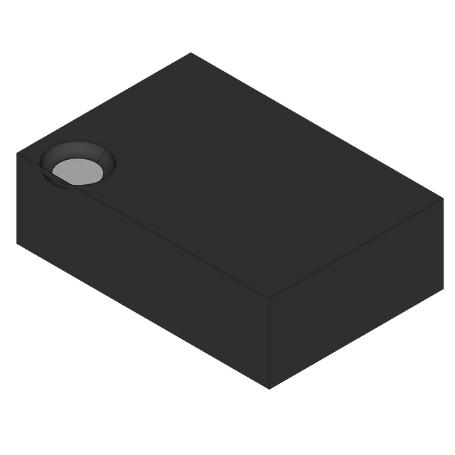
| 描述 | TVS DIODE 3.3VWM 12VC 6XSONTVS二极管阵列 DIODE ARRAY ESD TAPE-7 |
| 产品分类 | |
| 品牌 | NXP Semiconductors |
| 产品手册 | |
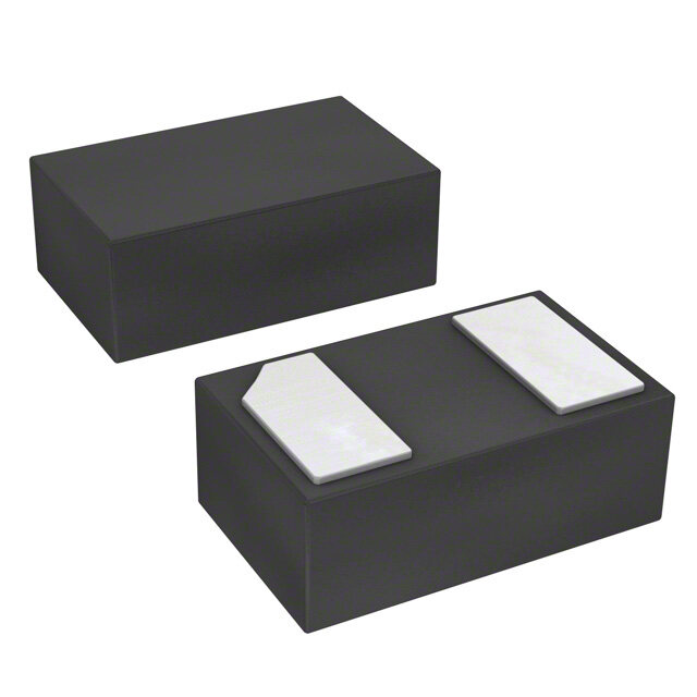
| 产品图片 |
|
| rohs | 符合RoHS无铅 / 符合限制有害物质指令(RoHS)规范要求 |
| 产品系列 | 二极管与整流器,TVS二极管,TVS二极管阵列,NXP Semiconductors PESD3V3L5UF,115- |
| 数据手册 | |
| 产品型号 | PESD3V3L5UF,115 |
| PCN封装 | |
| 不同频率时的电容 | 22pF @ 1MHz |
| 产品种类 | TVS二极管阵列 |
| 供应商器件封装 | 6-XSON,SOT886(1.45x1) |
| 其它名称 | 568-6744-1 |
| 击穿电压 | 5.6 V |
| 功率-峰值脉冲 | 25W |
| 包装 | 剪切带 (CT) |
| 单向通道 | 5 |
| 双向通道 | - |
| 商标 | NXP Semiconductors |
| 安装类型 | 表面贴装 |
| 安装风格 | SMD/SMT |
| 封装 | Reel |
| 封装/外壳 | 6-XFDFN |
| 封装/箱体 | SOT-886 |
| 尺寸 | 1.05 mm W x 1.5 mm L x 0.5 mm H |
| 峰值浪涌电流 | 2.5 A |
| 峰值脉冲功率耗散 | 25 W |
| 工作温度 | -65°C ~ 150°C (TA) |
| 工作电压 | 3.3 V |
| 工厂包装数量 | 5000 |
| 应用 | 通用 |
| 最大工作温度 | + 150 C |
| 最小工作温度 | - 65 C |
| 极性 | Unidirectional |
| 标准包装 | 1 |
| 电压-击穿(最小值) | 5.3V |
| 电压-反向关态(典型值) | 3.3V (最小值) |
| 电压-箝位(最大值)@Ipp | 12V |
| 电容 | 22 pF |
| 电流-峰值脉冲(10/1000µs) | 2.5A (8/20µs) |
| 电源线路保护 | 无 |
| 端接类型 | SMD/SMT |
| 类型 | 齐纳 |
| 系列 | PESD3V3L5U |
| 通道 | 4 Channels |
| 钳位电压 | 12 V |
| 零件号别名 | PESD3V3L5UF T/R |


- 商务部:美国ITC正式对集成电路等产品启动337调查
- 曝三星4nm工艺存在良率问题 高通将骁龙8 Gen1或转产台积电
- 太阳诱电将投资9.5亿元在常州建新厂生产MLCC 预计2023年完工
- 英特尔发布欧洲新工厂建设计划 深化IDM 2.0 战略
- 台积电先进制程称霸业界 有大客户加持明年业绩稳了
- 达到5530亿美元!SIA预计今年全球半导体销售额将创下新高
- 英特尔拟将自动驾驶子公司Mobileye上市 估值或超500亿美元
- 三星加码芯片和SET,合并消费电子和移动部门,撤换高东真等 CEO
- 三星电子宣布重大人事变动 还合并消费电子和移动部门
- 海关总署:前11个月进口集成电路产品价值2.52万亿元 增长14.8%


PDF Datasheet 数据手册内容提取
Important notice Dear Customer, On 7 February 2017 the former NXP Standard Product business became a new company with the tradename Nexperia. Nexperia is an industry leading supplier of Discrete, Logic and PowerMOS semiconductors with its focus on the automotive, industrial, computing, consumer and wearable application markets In data sheets and application notes which still contain NXP or Philips Semiconductors references, use the references to Nexperia, as shown below. Instead of http://www.nxp.com, http://www.philips.com/ or http://www.semiconductors.philips.com/, use http://www.nexperia.com Instead of sales.addresses@www.nxp.com or sales.addresses@www.semiconductors.philips.com, use salesaddresses@nexperia.com (email) Replace the copyright notice at the bottom of each page or elsewhere in the document, depending on the version, as shown below: - © NXP N.V. (year). All rights reserved or © Koninklijke Philips Electronics N.V. (year). All rights reserved Should be replaced with: - © Nexperia B.V. (year). All rights reserved. If you have any questions related to the data sheet, please contact our nearest sales office via e-mail or telephone (details via salesaddresses@nexperia.com). Thank you for your cooperation and understanding, Kind regards, Team Nexperia
PESDxL5UF; PESDxL5UV; PESDxL5UY Low capacitance unidirectional fivefold ESD protection diode arrays Rev. 02 — 8 January 2008 Product data sheet 1. Product profile 1.1 General description Low capacitance unidirectional fivefold ElectroStatic Discharge (ESD) protection diode arraysinsmallSurface-MountedDevice(SMD)plasticpackagesdesignedtoprotectupto five unidirectional signal lines from the damage caused by ESD and other transients. Table 1. Product overview Type number Package Package configuration NXP JEITA JEDEC PESD3V3L5UF SOT886 - MO-252 leadless ultra small PESD5V0L5UF SOT886 - MO-252 leadless ultra small PESD3V3L5UV SOT666 - - ultra small and flat lead PESD5V0L5UV SOT666 - - ultra small and flat lead PESD3V3L5UY SOT363 SC-88 - very small PESD5V0L5UY SOT363 SC-88 - very small 1.2 Features n ESD protection of up to five lines n Ultra low leakage current: I =5nA RM n Low diode capacitance n ESD protection up to20kV n Max. peak pulse power: P =25W n IEC61000-4-2; level4 (ESD) PP n Low clamping voltage: V =12V n IEC61000-4-5 (surge); I =2.5A CL PP 1.3 Applications n Computers and peripherals n Communication systems n Audio and video equipment n Portable electronics n Cellular handsets and accessories n Subscriber Identity Module (SIM) card protection
PESDxL5UF/V/Y NXP Semiconductors Low capacitance unidirectional fivefold ESD protection diode arrays 1.4 Quick reference data Table 2. Quick reference data T =25(cid:176) C unless otherwise specified. amb Symbol Parameter Conditions Min Typ Max Unit Per diode V reverse standoff voltage RWM PESD3V3L5UF - - 3.3 V PESD3V3L5UV PESD3V3L5UY PESD5V0L5UF - - 5.0 V PESD5V0L5UV PESD5V0L5UY C diode capacitance f=1MHz; V =0V d R PESD3V3L5UF - 22 28 pF PESD3V3L5UV PESD3V3L5UY PESD5V0L5UF - 16 19 pF PESD5V0L5UV PESD5V0L5UY 2. Pinning information Table 3. Pinning Pin Description Simplified outline Symbol PESD3V3L5UF; PESD5V0L5UF 1 cathode (diode1) 1 2 3 2 common anode 1 6 3 cathode (diode2) 2 5 4 cathode (diode3) 3 4 5 cathode (diode4) 006aaa159 6 5 4 6 cathode (diode5) bottom view PESD3V3L5UV; PESD5V0L5UV 1 cathode (diode1) 6 5 4 2 common anode 1 6 3 cathode (diode2) 2 5 4 cathode (diode3) 3 4 5 cathode (diode4) 006aaa159 1 2 3 6 cathode (diode5) PESDXL5UF_V_Y_2 © NXP B.V. 2008. All rights reserved. Product data sheet Rev. 02 — 8 January 2008 2 of 17
PESDxL5UF/V/Y NXP Semiconductors Low capacitance unidirectional fivefold ESD protection diode arrays Table 3. Pinning …continued Pin Description Simplified outline Symbol PESD3V3L5UY; PESD5V0L5UY 1 cathode (diode1) 6 5 4 2 common anode 1 6 3 cathode (diode2) 2 5 4 cathode (diode3) 3 4 5 cathode (diode4) 1 2 3 006aaa159 6 cathode (diode5) 3. Ordering information Table 4. Ordering information Type number Package Name Description Version PESD3V3L5UF XSON6 plastic extremely thin small outline package; SOT886 noleads; 6terminals; body 1· 1.45· 0.5mm PESD5V0L5UF PESD3V3L5UV - plastic surface-mounted package; 6leads SOT666 PESD5V0L5UV PESD3V3L5UY SC-88 plastic surface-mounted package; 6leads SOT363 PESD5V0L5UY 4. Marking Table 5. Marking codes Type number Marking code[1] PESD3V3L5UF A1 PESD5V0L5UF A2 PESD3V3L5UV E1 PESD5V0L5UV E2 PESD3V3L5UY K3* PESD5V0L5UY K4* [1] * = -: made in Hong Kong * = p: made in Hong Kong * = t: made in Malaysia * = W: made in China PESDXL5UF_V_Y_2 © NXP B.V. 2008. All rights reserved. Product data sheet Rev. 02 — 8 January 2008 3 of 17
PESDxL5UF/V/Y NXP Semiconductors Low capacitance unidirectional fivefold ESD protection diode arrays 5. Limiting values Table 6. Limiting values In accordance with the Absolute Maximum Rating System (IEC 60134). Symbol Parameter Conditions Min Max Unit Per diode P peak pulse power t =8/20m s [1][2] - 25 W PP p I peak pulse current t =8/20m s [1][2] - 2.5 A PP p Per device T junction temperature - 150 (cid:176) C j T ambient temperature - 65 +150 (cid:176) C amb T storage temperature - 65 +150 (cid:176) C stg [1] Non-repetitive current pulse 8/20m s exponential decay waveform according to IEC61000-4-5. [2] Measured from pin 1, 3, 4, 5 or6 to pin2. Table 7. ESD maximum ratings T =25(cid:176) C unless otherwise specified. amb Symbol Parameter Conditions Min Max Unit Per diode V electrostatic discharge voltage IEC61000-4-2 [1][2] - 20 kV ESD (contact discharge) MIL-STD-883(human - 10 kV body model) [1] Device stressed with ten non-repetitive ESDpulses. [2] Measured from pin 1, 3, 4, 5 or6 to pin2. Table 8. ESD standards compliance Standard Conditions Per diode IEC61000-4-2; level4 (ESD) >15kV(air); >8kV(contact) MIL-STD-883; class3 (human body model) >4kV PESDXL5UF_V_Y_2 © NXP B.V. 2008. All rights reserved. Product data sheet Rev. 02 — 8 January 2008 4 of 17
PESDxL5UF/V/Y NXP Semiconductors Low capacitance unidirectional fivefold ESD protection diode arrays 001aaa631 001aaa630 IPP 120 100 % IPP 100 % IPP; 8 m s 90 % (%) 80 e- t 50 % IPP; 20 m s 40 10 % tr = 0.7 ns to 1 ns t 0 0 10 20 30 40 30 ns t (m s) 60 ns Fig 1. 8/20m s pulse waveform according to Fig 2. ESD pulse waveform according to IEC61000-4-5 IEC61000-4-2 6. Characteristics Table 9. Characteristics T =25(cid:176) C unless otherwise specified. amb Symbol Parameter Conditions Min Typ Max Unit Per diode V reverse standoff voltage RWM PESD3V3L5UF - - 3.3 V PESD3V3L5UV PESD3V3L5UY PESD5V0L5UF - - 5.0 V PESD5V0L5UV PESD5V0L5UY I reverse leakage current RM PESD3V3L5UF V =3.3V - 75 300 nA RWM PESD3V3L5UV PESD3V3L5UY PESD5V0L5UF V =5.0V - 5 25 nA RWM PESD5V0L5UV PESD5V0L5UY V breakdown voltage I =1mA BR R PESD3V3L5UF 5.3 5.6 5.9 V PESD3V3L5UV PESD3V3L5UY PESD5V0L5UF 6.4 6.8 7.2 V PESD5V0L5UV PESD5V0L5UY PESDXL5UF_V_Y_2 © NXP B.V. 2008. All rights reserved. Product data sheet Rev. 02 — 8 January 2008 5 of 17
PESDxL5UF/V/Y NXP Semiconductors Low capacitance unidirectional fivefold ESD protection diode arrays Table 9. Characteristics …continued T =25(cid:176) C unless otherwise specified. amb Symbol Parameter Conditions Min Typ Max Unit C diode capacitance f=1MHz; d V =0V R PESD3V3L5UF - 22 28 pF PESD3V3L5UV PESD3V3L5UY PESD5V0L5UF - 16 19 pF PESD5V0L5UV PESD5V0L5UY V clamping voltage [1][2] CL PESD3V3L5UF I =1A - - 10 V PP PESD3V3L5UV PESD3V3L5UY PESD3V3L5UF I =2.5A - - 12 V PP PESD3V3L5UV PESD3V3L5UY PESD5V0L5UF I =1A - - 10 V PP PESD5V0L5UV PESD5V0L5UY PESD5V0L5UF I =2.5A - - 12 V PP PESD5V0L5UV PESD5V0L5UY r differential resistance I =1mA dif R PESD3V3L5UF - - 200 W PESD3V3L5UV PESD3V3L5UY PESD5V0L5UF - - 100 W PESD5V0L5UV PESD5V0L5UY [1] Non-repetitive current pulse 8/20m s exponential decay waveform according to IEC61000-4-5. [2] Measured from pin 1, 3, 4, 5 or6 to pin2. PESDXL5UF_V_Y_2 © NXP B.V. 2008. All rights reserved. Product data sheet Rev. 02 — 8 January 2008 6 of 17
PESDxL5UF/V/Y NXP Semiconductors Low capacitance unidirectional fivefold ESD protection diode arrays 102 006aab139 1.2 006aab140 PPP PPP(25(cid:176)C) 1.0 PPP (W) 0.8 10 0.6 0.4 0.2 1 0 1 10 102 103 104 0 50 100 150 tp (m s) Tj ((cid:176)C) T =25(cid:176) C amb Fig 3. Peak pulse power as a function of exponential Fig 4. Relative variation of peak pulse power as a pulse duration; typical values function of junction temperature; typical values 006aab141 006aab142 25 10 Cd (pF) 20 IR IR(25(cid:176)C) 15 (1) 1 (2) 10 5 0 10- 1 0 1 2 3 4 5 - 75 - 25 25 75 125 175 VR (V) Tj ((cid:176)C) f=1MHz; T =25(cid:176) C amb (1) PESD3V3L5UF; PESD3V3L5UV; PESD3V3L5UY (2) PESD5V0L5UF; PESD5V0L5UV; PESD5V0L5UY Fig 5. Diode capacitance as a function of reverse Fig 6. Relative variation of reverse current as a voltage; typical values function of junction temperature; typical values PESDXL5UF_V_Y_2 © NXP B.V. 2008. All rights reserved. Product data sheet Rev. 02 — 8 January 2008 7 of 17
PESDxL5UF/V/Y NXP Semiconductors Low capacitance unidirectional fivefold ESD protection diode arrays I - VCL- VBR - VRWM V - IRM - IR - + P-N - IPP 006aaa407 Fig 7. V-Icharacteristics for a unidirectional ESDprotection diode PESDXL5UF_V_Y_2 © NXP B.V. 2008. All rights reserved. Product data sheet Rev. 02 — 8 January 2008 8 of 17
PESDxL5UF/V/Y NXP Semiconductors Low capacitance unidirectional fivefold ESD protection diode arrays ESD TESTER 4 GHz DIGITAL RG 223/U OSCILLOSCOPE RZ 450 W 50 W coax 10· ATTENUATOR (1) CZ 50 W DUT Device Under Test IEC 61000-4-2 network (1): attenuator is only used for open CZ = 150 pF; RZ = 330 W socket high voltage measurements vertical scale = 200 V/div vertical scale = 5 V/div horizontal scale = 50 ns/div horizontal scale = 50 ns/div PESD5V0L5UF/V/Y GND1 GND PESD3V3L5UF/V/Y GND2 unclamped +1 kV ESD voltage waveform clamped +1 kV ESD voltage waveform (IEC 61000-4-2 network) (IEC 61000-4-2 network) GND GND vertical scale = 200 V/div vertical scale = 5 V/div horizontal scale = 50 ns/div horizontal scale = 50 ns/div unclamped - 1 kV ESD voltage waveform clamped - 1 kV ESD voltage waveform (IEC 61000-4-2 network) (IEC 61000-4-2 network) 006aab143 Fig 8. ESD clamping test setup and waveforms PESDXL5UF_V_Y_2 © NXP B.V. 2008. All rights reserved. Product data sheet Rev. 02 — 8 January 2008 9 of 17
PESDxL5UF/V/Y NXP Semiconductors Low capacitance unidirectional fivefold ESD protection diode arrays 7. Application information Thedevicesaredesignedfortheprotectionofuptofiveunidirectionaldataorsignallines from the damage caused by ESD and surge pulses. The devices may be used on lines where the signal polarities are both, positive and negative with respect to ground. The devices provide a surge capability of 25W per line for an 8/20m s waveform each. high-speed data lines high-speed data lines DUT DUT GND GND 006aab144 006aab145 Fig 9. Typical application for unidirectional Fig 10. Typical application for bidirectional application application of five lines of four lines Circuit board layout and protection device placement Circuit board layout is critical for the suppression of ESD, Electrical Fast Transient (EFT) and surge transients. The following guidelines are recommended: 1. Place the device as close to the input terminal or connector as possible. 2. The path length between the device and the protected line should be minimized. 3. Keep parallel signal paths to a minimum. 4. Avoid running protected conductors in parallel with unprotected conductors. 5. Minimize all Printed-Circuit Board (PCB) conductive loops including power and ground loops. 6. Minimize the length of the transient return path to ground. 7. Avoid using shared transient return paths to a common ground point. 8. Ground planes should be used whenever possible. For multilayer PCBs, use ground vias. PESDXL5UF_V_Y_2 © NXP B.V. 2008. All rights reserved. Product data sheet Rev. 02 — 8 January 2008 10 of 17
PESDxL5UF/V/Y NXP Semiconductors Low capacitance unidirectional fivefold ESD protection diode arrays 8. Package outline 1.05 0.50 1.7 0.6 0.95 max 1.5 0.5 0.04 0.6 max 6 5 4 0.25 3 4 0.17 0.3 0.1 0.5 1.7 1.3 1.5 2 5 1.5 1.1 1.4 pin 1 index 0.5 1 6 1 2 3 0.27 0.18 0.40 0.35 0.5 0.17 0.08 0.32 0.27 1 Dimensions in mm 04-07-22 Dimensions in mm 04-11-08 Fig 11. Package outline PESDxL5UF(SOT886) Fig 12. Package outline PESDxL5UV(SOT666) 2.2 1.1 1.8 0.8 6 5 4 0.45 0.15 2.2 1.35 2.0 1.15 pin 1 index 1 2 3 0.3 0.25 0.65 0.2 0.10 1.3 Dimensions in mm 06-03-16 Fig 13. Package outline PESDxL5UY(SOT363/SC-88) PESDXL5UF_V_Y_2 © NXP B.V. 2008. All rights reserved. Product data sheet Rev. 02 — 8 January 2008 11 of 17
PESDxL5UF/V/Y NXP Semiconductors Low capacitance unidirectional fivefold ESD protection diode arrays 9. Packing information Table 10. Packing methods The indicated -xxx are the last three digits of the 12NC ordering code.[1] Type number Package Description Packing quantity 3000 4000 5000 8000 10000 PESD3V3L5UF SOT886 4mm pitch, 8mm tape and reel; T1 [2] - - -115 - - 4mm pitch, 8mm tape and reel; T4 [3] - - -132 - - PESD5V0L5UF SOT886 4mm pitch, 8mm tape and reel; T1 [2] - - -115 - - 4mm pitch, 8mm tape and reel; T4 [3] - - -132 - - PESD3V3L5UV SOT666 2mm pitch, 8mm tape and reel - - - -315 - 4mm pitch, 8mm tape and reel - -115 - - - PESD5V0L5UV SOT666 2mm pitch, 8mm tape and reel - - - -315 - 4mm pitch, 8mm tape and reel - -115 - - - PESD3V3L5UY SOT363 4mm pitch, 8mm tape and reel; T1 [2] -115 - - - -135 4mm pitch, 8mm tape and reel; T2 [4] -125 - - - -165 PESD5V0L5UY SOT363 4mm pitch, 8mm tape and reel; T1 [2] -115 - - - -135 4mm pitch, 8mm tape and reel; T2 [4] -125 - - - -165 [1] For further information and the availability of packing methods, seeSection13. [2] T1: normal taping [3] T4: 90(cid:176) rotated reverse taping [4] T2: reverse taping 10. Soldering 1.250 0.675 0.370 (6· ) 0.500 1.700 solder lands 0.500 solder paste 0.270 (6· ) occupied area Dimensions in mm 0.325 0.425 (6· ) (6·) sot886_fr Reflow soldering is the only recommended soldering method. Fig 14. Reflow soldering footprint PESDxL5UF(SOT886) PESDXL5UF_V_Y_2 © NXP B.V. 2008. All rights reserved. Product data sheet Rev. 02 — 8 January 2008 12 of 17
PESDxL5UF/V/Y NXP Semiconductors Low capacitance unidirectional fivefold ESD protection diode arrays 2.75 2.45 2.10 1.60 0.15 (4· ) 0.40 (6· ) 2.001.701.00 0(2.5·5) 0.30 (2· ) 0.375 (4· ) 1.20 2.20 2.50 solder lands placement area 0.075 solder resist occupied area Dimensions in mm Reflow soldering is the only recommended soldering method. Fig 15. Reflow soldering footprint PESDxL5UV(SOT666) 2.65 0.60 (2· ) 0.40 2.35 (2· ) 0.90 2.10 solder lands solder paste 0.50 (4· ) solder resist occupied area 0.50 (4· ) 1.20 Dimensions in mm 2.40 sot363 Fig 16. Reflow soldering footprint PESDxL5UY(SOT363/SC-88) PESDXL5UF_V_Y_2 © NXP B.V. 2008. All rights reserved. Product data sheet Rev. 02 — 8 January 2008 13 of 17
PESDxL5UF/V/Y NXP Semiconductors Low capacitance unidirectional fivefold ESD protection diode arrays 5.25 4.50 0.30 1.00 4.00 solder lands 1.15 solder resist 3.75 occupied area transport direction during soldering Dimensions in mm sot363 Fig 17. Wave soldering footprint PESDxL5UY(SOT363/SC-88) PESDXL5UF_V_Y_2 © NXP B.V. 2008. All rights reserved. Product data sheet Rev. 02 — 8 January 2008 14 of 17
PESDxL5UF/V/Y NXP Semiconductors Low capacitance unidirectional fivefold ESD protection diode arrays 11. Revision history Table 11. Revision history Document ID Release date Data sheet status Change notice Supersedes PESDXL5UF_V_Y_2 20080108 Product data sheet - PESD3V3L5UV_ PESD5V0L5UV_1 PESD3V3L5UY_ PESD5V0L5UY_1 Modifications: • The format of this data sheet has been redesigned to comply with the new identity guidelines of NXP Semiconductors. • Legal texts have been adapted to the new company name where appropriate. • Type numbers PESD3V3L5UF and PESD5V0L5UF added • Table 1 “Product overview”: added • Section 4 “Marking”: marking code for PESD3V3L5UV amended • Section 4 “Marking”: marking code for PESD5V0L5UV amended • Section 4 “Marking”: marking code for PESD3V3L5UY amended • Section 4 “Marking”: marking code for PESD5V0L5UY amended • Figure7: added • Section 9 “Packing information”: added • Section 10 “Soldering”: added • Section 12 “Legal information”: updated PESD3V3L5UV_PESD5V0L5UV_1 20040323 Product specification - - PESD3V3L5UY_PESD5V0L5UY_1 20040323 Product specification - - PESDXL5UF_V_Y_2 © NXP B.V. 2008. All rights reserved. Product data sheet Rev. 02 — 8 January 2008 15 of 17
PESDxL5UF/V/Y NXP Semiconductors Low capacitance unidirectional fivefold ESD protection diode arrays 12. Legal information 12.1 Data sheet status Document status[1][2] Product status[3] Definition Objective [short] data sheet Development This document contains data from the objective specification for product development. Preliminary [short] data sheet Qualification This document contains data from the preliminary specification. Product [short] data sheet Production This document contains the product specification. [1] Please consult the most recently issued document before initiating or completing a design. [2] The term ‘short data sheet’ is explained in section “Definitions”. [3] Theproductstatusofdevice(s)describedinthisdocumentmayhavechangedsincethisdocumentwaspublishedandmaydifferincaseofmultipledevices.Thelatestproductstatus information is available on the Internet at URLhttp://www.nxp.com. 12.2 Definitions malfunction of an NXP Semiconductors product can reasonably be expected to result in personal injury, death or severe property or environmental damage. NXP Semiconductors accepts no liability for inclusion and/or use of Draft —The document is a draft version only. The content is still under NXP Semiconductors products in such equipment or applications and internal review and subject to formal approval, which may result in therefore such inclusion and/or use is at the customer’s own risk. modifications or additions. NXP Semiconductors does not give any representations or warranties as to the accuracy or completeness of Applications —Applications that are described herein for any of these informationincludedhereinandshallhavenoliabilityfortheconsequencesof products are for illustrative purposes only. NXP Semiconductors makes no use of such information. representation or warranty that such applications will be suitable for the specified use without further testing or modification. Short data sheet —A short data sheet is an extract from a full data sheet withthesameproducttypenumber(s)andtitle.Ashortdatasheetisintended Limiting values —Stress above one or more limiting values (as defined in forquickreferenceonlyandshouldnotbereliedupontocontaindetailedand theAbsoluteMaximumRatingsSystemofIEC60134)maycausepermanent full information. For detailed and full information see the relevant full data damagetothedevice.Limitingvaluesarestressratingsonlyandoperationof sheet, which is available on request via the local NXP Semiconductors sales the device at these or any other conditions above those given in the office. In case of any inconsistency or conflict with the short data sheet, the Characteristics sections of this document is not implied. Exposure to limiting full data sheet shall prevail. values for extended periods may affect device reliability. Terms and conditions of sale —NXP Semiconductors products are sold 12.3 Disclaimers subjecttothegeneraltermsandconditionsofcommercialsale,aspublished athttp://www.nxp.com/profile/terms, including those pertaining to warranty, intellectual property rights infringement and limitation of liability, unless General —Information in this document is believed to be accurate and explicitly otherwise agreed to in writing by NXP Semiconductors. In case of reliable.However,NXPSemiconductorsdoesnotgiveanyrepresentationsor any inconsistency or conflict between information in this document and such warranties,expressedorimplied,astotheaccuracyorcompletenessofsuch terms and conditions, the latter will prevail. information and shall have no liability for the consequences of use of such No offer to sell or license —Nothing in this document may be interpreted information. or construed as an offer to sell products that is open for acceptance or the Right to make changes —NXPSemiconductorsreservestherighttomake grant,conveyanceorimplicationofanylicenseunderanycopyrights,patents changes to information published in this document, including without or other industrial or intellectual property rights. limitation specifications and product descriptions, at any time and without notice.Thisdocumentsupersedesandreplacesallinformationsuppliedprior to the publication hereof. 12.4 Trademarks Suitability for use —NXP Semiconductors products are not designed, Notice:Allreferencedbrands,productnames,servicenamesandtrademarks authorized or warranted to be suitable for use in medical, military, aircraft, are the property of their respective owners. space or life support equipment, nor in applications where failure or 13. Contact information For additional information, please visit:http://www.nxp.com For sales office addresses, send an email to:salesaddresses@nxp.com PESDXL5UF_V_Y_2 © NXP B.V. 2008. All rights reserved. Product data sheet Rev. 02 — 8 January 2008 16 of 17
PESDxL5UF/V/Y NXP Semiconductors Low capacitance unidirectional fivefold ESD protection diode arrays 14. Contents 1 Product profile. . . . . . . . . . . . . . . . . . . . . . . . . . 1 1.1 General description. . . . . . . . . . . . . . . . . . . . . . 1 1.2 Features . . . . . . . . . . . . . . . . . . . . . . . . . . . . . . 1 1.3 Applications . . . . . . . . . . . . . . . . . . . . . . . . . . . 1 1.4 Quick reference data. . . . . . . . . . . . . . . . . . . . . 2 2 Pinning information. . . . . . . . . . . . . . . . . . . . . . 2 3 Ordering information. . . . . . . . . . . . . . . . . . . . . 3 4 Marking. . . . . . . . . . . . . . . . . . . . . . . . . . . . . . . . 3 5 Limiting values. . . . . . . . . . . . . . . . . . . . . . . . . . 4 6 Characteristics. . . . . . . . . . . . . . . . . . . . . . . . . . 5 7 Application information. . . . . . . . . . . . . . . . . . 10 8 Package outline . . . . . . . . . . . . . . . . . . . . . . . . 11 9 Packing information. . . . . . . . . . . . . . . . . . . . . 12 10 Soldering . . . . . . . . . . . . . . . . . . . . . . . . . . . . . 12 11 Revision history. . . . . . . . . . . . . . . . . . . . . . . . 15 12 Legal information. . . . . . . . . . . . . . . . . . . . . . . 16 12.1 Data sheet status . . . . . . . . . . . . . . . . . . . . . . 16 12.2 Definitions. . . . . . . . . . . . . . . . . . . . . . . . . . . . 16 12.3 Disclaimers. . . . . . . . . . . . . . . . . . . . . . . . . . . 16 12.4 Trademarks. . . . . . . . . . . . . . . . . . . . . . . . . . . 16 13 Contact information. . . . . . . . . . . . . . . . . . . . . 16 14 Contents. . . . . . . . . . . . . . . . . . . . . . . . . . . . . . 17 Pleasebeawarethatimportantnoticesconcerningthisdocumentandtheproduct(s) described herein, have been included in section ‘Legal information’. © NXP B.V. 2008. All rights reserved. For more information, please visit: http://www.nxp.com For sales office addresses, please send an email to: salesaddresses@nxp.com Date of release: 8 January 2008 Document identifier: PESDXL5UF_V_Y_2