 Datasheet下载
- 型号: PCM3168APAP
- 制造商: Texas Instruments
- 库位|库存: xxxx|xxxx
- 要求:
| 数量阶梯 | 香港交货 | 国内含税 |
| +xxxx | $xxxx | ¥xxxx |
查看当月历史价格
查看今年历史价格
PCM3168APAP产品简介:
ICGOO电子元器件商城为您提供PCM3168APAP由Texas Instruments设计生产,在icgoo商城现货销售,并且可以通过原厂、代理商等渠道进行代购。 PCM3168APAP价格参考。Texas InstrumentsPCM3168APAP封装/规格:接口 - 编解码器, Audio Interface 24 b Serial 64-HTQFP (10x10)。您可以下载PCM3168APAP参考资料、Datasheet数据手册功能说明书,资料中有PCM3168APAP 详细功能的应用电路图电压和使用方法及教程。
Texas Instruments(德州仪器)的PCM3168APAP是一款接口编解码器,主要用于音频信号的处理和转换。以下是其典型的应用场景:

1. 多通道音频系统:
   PCM3168A支持8通道24位立体声音频ADC/DAC,适用于需要多通道音频输入/输出的设备,如专业音频混音器、录音设备和会议系统。

2. 家庭影院和音响设备:
   该芯片可用于家庭影院接收器、AV放大器和其他高保真音响设备中,提供高质量的音频编解码功能,支持多种采样率(高达192kHz),满足高端音频需求。

3. 语音通信设备:
   在IP电话、视频会议系统或VoIP网关中,PCM3168A可以实现清晰的语音编解码,同时支持灵活的接口配置(如I2S、TDM等),适应不同的通信协议。

4. 便携式音频设备:
   由于其低功耗设计,PCM3168A适合用于便携式音频播放器、录音笔或其他电池供电的音频设备,确保长时间运行的同时保持高音质。

5. 汽车音响系统:
   在车载娱乐系统中,这款编解码器可用于处理来自多个麦克风或扬声器的音频信号,支持高分辨率音频播放,提升车内音效体验。

6. 工业和医疗应用:
   在需要精确音频信号采集和传输的领域,例如工业监测设备或医疗超声波设备中,PCM3168A的高性能和稳定性使其成为理想选择。

总之,PCM3168APAP以其多通道能力、高分辨率和灵活接口特性,广泛应用于消费电子、通信、工业和汽车等领域,为各种音频相关产品提供可靠的支持。
| 参数 | 数值 |
| ADC/DAC数 | 6 / 8 |
| ADC数量 | 6 |
| 产品目录 | 集成电路 (IC)半导体 |
| DAC数量 | 8 |
| 描述 | IC 24-BIT AUDIO CODEC 64-HTQFP接口—CODEC 24B,96/192kHz,6ch-in 8ch-out Aud CODEC |
| 产品分类 | |
| 品牌 | Texas Instruments |
| 产品手册 | |
| 产品图片 |
|
| rohs | 符合RoHS无铅 / 符合限制有害物质指令(RoHS)规范要求 |
| 产品系列 | 接口 IC,接口—CODEC,Texas Instruments PCM3168APAP- |
| 数据手册 | |
| 产品型号 | PCM3168APAP |
| PCN组件/产地 | |
| THD+噪声 | - 93 dB ADC/- 94 dB DAC |
| 三角积分 | 是 |
| 产品目录页面 | |
| 产品种类 | 接口—CODEC |
| 供应商器件封装 | 64-HTQFP(10x10) |
| 信噪比 | 107 dB ADC/112 dB DAC |
| 信噪比,ADC/DAC(db)(典型值) | 107 / 112(差分),104 / 112(单端) |
| 其它名称 | 296-23899-5 |
| 分辨率 | 24 bit |
| 分辨率(位) | 24 b |
| 动态范围,ADC/DAC(db)(典型值) | 107 / 112(差分),104 / 112(单端) |
| 包装 | 托盘 |
| 单位重量 | 258.200 mg |
| 商标 | Texas Instruments |
| 安装类型 | 表面贴装 |
| 安装风格 | SMD/SMT |
| 封装 | Tray |
| 封装/外壳 | 64-TQFP 裸露焊盘 |
| 封装/箱体 | HTQFP-64 |
| 工作温度 | -40°C ~ 85°C |
| 工厂包装数量 | 160 |
| 接口类型 | Serial (I2C, SPI) |
| 数据接口 | 串行 |
| 最大工作温度 | + 85 C |
| 最小工作温度 | - 40 C |
| 标准包装 | 160 |
| 电压-电源,数字 | 3 V ~ 3.6 V |
| 电压-电源,模拟 | 4.5 V ~ 5.5 V |
| 类型 | 音频 |
| 系列 | PCM3168A |
| 转换速率 | 192 kHz |


PDF Datasheet 数据手册内容提取
Product Sample & Technical Tools & Support & Reference Folder Buy Documents Software Community Design PCM3168A Burr-Brown Audio SBAS452A–SEPTEMBER2008–REVISEDJANUARY2016 PCM3168A 24-Bit, 96-kHz/192-kHz, 6-In/8-Out Audio Codec With Differential Input/Output 1 Features • MultiFunctionsThroughH/WControl: • 24-BitΔΣADCandDAC – AudioI/FMode/FormatSelect 1 • Six-ChanneLADC: – DigitalDe-EmphasisFilter:44.1kHzforDAC – HighPerformance:DifferentialandSingle- • ExternalResetPin: Ended,f =48kHz – ADC/DACSimultaneous S – THD+N: –93dB(DifferentialandSingle- • AudioInterfaceMode: Ended) – ADC/DACIndependentMasterandSlave – SNR:107dB(Differential), • AudioDataFormat: 104dB(Single-Ended) – ADC/DACIndependent I2S™,Left-Justified, – DynamicRange:107dB(Differential), Right-Justified,DSP,TDM 104dB(Single-Ended) • PowerSupplies:5VforAnalogand3.3Vfor – SamplingRate:8kHzto96kHz Digital – SystemClock:256fS,384fS,512fS,768fS • Package:HTQFP-64 – DifferentialVoltageInput:2VRMS • OperatingTemperatureRange: – Single-EndedVoltageInput:1VRMS – ConsumerGrade: –40°Cto85°C – DecimationFilter: – AutomotiveAudioGrade: –40°Cto105°C – PassbandRipple: ±0.035dB 2 Applications – StopBandAttenuation: –75dB – On-Chip,HighpassFilter: • CarAudioExternalAmplifiers 0.96Hzatf =48kHz • CarAudioAVNApplications S – OverflowFlag • HomeTheaters • Eight-ChannelDAC: • AVReceivers – HighPerformance:Differential,f =48kHz S 3 Description – THD+N: –94dB The PCM3168A device is a high-performance, single- – SNR:112dB chip, 24-bit, 6-in/8-out, audio coder and decoder – DynamicRange:112dB (codecs) with single-ended and differential-selectable – SamplingRate:8kHzto192kHz analoginputsanddifferentialoutputs. – SystemClock:128f ,192f ,256f ,384f , S S S S DeviceInformation(1) 512f ,768f S S PARTNUMBER PACKAGE BODYSIZE(NOM) – DifferentialVoltageOutput:8V PP PCM3168A HTQFP(64) 10.00mmx10.00mm – AnalogLowpassFilterIncluded (1) For all available packages, see the orderable addendum at – 4x/8xOversamplingDigitalFilter: theendofthedatasheet. – PassbandRipple: ±0.0018dB SimplifiedApplicationDiagram – StopBandAttenuation: –75dB – ZeroFlag • FlexibleModeControl: DSP – Four-WireSPI™,Two-WireI2C™Compatible SerialControlInterfaceorHardwareControl O R • MultiFunctionsThroughSPIorI2CI/F: TDM F/ZE I2C V O – AudioI/FModeandFormatSelectforADC andDAC x4 TAS5424 x4 6 Channel C-Q1 – DigitalAttenuationandSoftMuteforADCand Differential Input PCM3168A Output Analog Audio Filters Filters DAC Source x4 TACS-5Q4124 x4 – DigitalDe-Emphasis:32,44.1,and48kHzfor DAC 1 An IMPORTANT NOTICE at the end of this data sheet addresses availability, warranty, changes, use in safety-critical applications, intellectualpropertymattersandotherimportantdisclaimers.PRODUCTIONDATA.
PCM3168A SBAS452A–SEPTEMBER2008–REVISEDJANUARY2016 www.ti.com Table of Contents 1 Features.................................................................. 1 8.14 TimingRequirements:SCLandSDAControl Interface................................................................... 15 2 Applications........................................................... 1 8.15 TypicalCharacteristics..........................................19 3 Description............................................................. 1 9 DetailedDescription............................................ 24 4 RevisionHistory..................................................... 2 9.1 Overview.................................................................24 5 Description(continued)......................................... 3 9.2 FunctionalBlockDiagram.......................................24 6 DeviceComparisonTable..................................... 3 9.3 FeatureDescription.................................................25 7 PinConfigurationandFunctions......................... 4 9.4 DeviceFunctionalModes........................................31 8 Specifications......................................................... 7 9.5 RegisterMaps.........................................................36 8.1 AbsoluteMaximumRatings .....................................7 10 ApplicationandImplementation........................ 51 8.2 ESDRatings..............................................................8 10.1 ApplicationInformation..........................................51 8.3 RecommendedOperatingConditions.......................8 10.2 TypicalApplication................................................51 8.4 ThermalInformation..................................................8 10.3 SystemExamples.................................................53 8.5 ElectricalCharacteristics...........................................9 11 PowerSupplyRecommendations..................... 54 8.6 TimingRequirements:SystemClock......................12 12 Layout................................................................... 55 8.7 TimingRequirements:Power-OnReset.................13 12.1 LayoutGuidelines.................................................55 8.8 TimingRequirements:AudioInterfaceforLeft- Justified,Right-Justified,andI2S(SlaveMode)......13 12.2 LayoutExample....................................................57 13 DeviceandDocumentationSupport................. 58 8.9 TimingRequirements:AudioInterfaceforLeft- Justified,Right-Justified,andI2S(MasterMode)....13 13.1 DeviceSupport......................................................58 8.10 TimingRequirements:AudioInterfaceforDSPand 13.2 DocumentationSupport........................................58 TDM(SlaveMode)...................................................14 13.3 CommunityResources..........................................58 8.11 TimingRequirements:AudioInterfaceforDSPand 13.4 Trademarks...........................................................58 TDM(MasterMode).................................................14 13.5 ElectrostaticDischargeCaution............................58 8.12 TimingRequirements:DACOutputsandADC 13.6 Glossary................................................................58 Outputs..................................................................... 14 14 Mechanical,Packaging,andOrderable 8.13 TimingRequirements:Four-WireSerialControl Information........................................................... 58 Interface................................................................... 15 4 Revision History NOTE:Pagenumbersforpreviousrevisionsmaydifferfrompagenumbersinthecurrentversion. ChangesfromOriginal(September2008)toRevisionA Page • AddedESDRatingstable,FeatureDescriptionsection,DeviceFunctionalModessection,Applicationand Implementationsection,PowerSupplyRecommendationssection,Layoutsection,DeviceandDocumentation Supportsection,andMechanical,Packaging,andOrderableInformationsection. .............................................................. 1 2 SubmitDocumentationFeedback Copyright©2008–2016,TexasInstrumentsIncorporated ProductFolderLinks:PCM3168A
PCM3168A www.ti.com SBAS452A–SEPTEMBER2008–REVISEDJANUARY2016 5 Description (continued) The six-channel, 24-bit analog-to-digital converter (ADC) employs a delta-sigma (ΔΣ) modulator and supports 8-kHzto96-kHzsamplingratesanda16-bit/24-bitwidthdigitalaudiooutputwordontheaudiointerface. The eight-channel, 24-bit digital-to-analog converter (DAC) employs a ΔΣ modulator and supports 8-kHz to 192-kHz sampling rates and a 16-bit/24-bit width digital audio input word on the audio interface. Each audio interface supports I2S, left-justified, right-justified, and DSP formats with 16-bit/24-bit word width. In addition, the PCM3168Adevicesupportsthetime-division-multiplexed(TDM)format. The PCM3168A device can be controlled through a four-wire, SPI-compatible interface, or two-wire, I2C- compatible serial interface in software, which provides access to all functions including digital attenuation, soft mute, de-emphasis, and so forth. Also, hardware control mode provides a subset of user-programmable functions through four control pins. The PCM3168A device is available in a 12-mm × 12-mm (10-mm × 10-mm body)HTQFP-64PowerPAD™package. 6 Device Comparison Table PART ADCs DACs CONTROL AUTOMOTIVEGRADE PCM3168A 6 8 SPI,I2C No PCM3168A-Q1 6 8 SPI,I2C Yes Copyright©2008–2016,TexasInstrumentsIncorporated SubmitDocumentationFeedback 3 ProductFolderLinks:PCM3168A
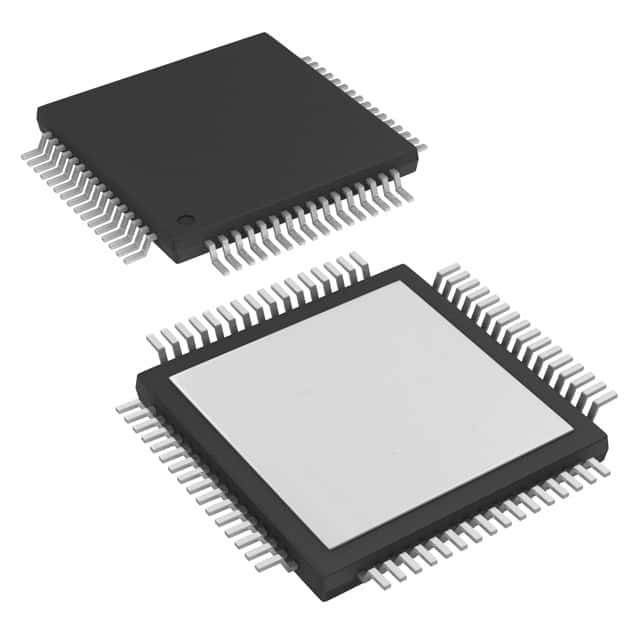
PCM3168A SBAS452A–SEPTEMBER2008–REVISEDJANUARY2016 www.ti.com 7 Pin Configuration and Functions PAPPackage 64-PinHTQFPWithPowerPAD TopView D2 D1 D1 1 + - + - FA FA + - + - + - + - DA AD N6 N6 N5 N5 RE RE N4 N4 N3 N3 N2 N2 N1 N1 GN CC VI VI VI VI V A VI VI VI VI VI VI VI VI A V 64 63 62 61 60 59 58 57 56 55 54 53 52 51 50 49 VCOMAD 1 48 MODE AGNDAD2 2 47 DGND1 VCCAD2 3 46 VDD1 RST 4 45 MS/ADR0/MD0 OVF 5 44 MDO/ADR1/MD1 LRCKAD 6 43 MDI/SDA/DEMP BCKAD 7 PCM3168A 42 MC/SCL/FMT DOUT1 8 PCM3168A-Q1 41 SCKI PowerPAD DOUT2 9 40 DIN4 (Connected to Analog Ground) DOUT3 10 39 DIN3 DGND2 11 38 DIN2 VDD2 12 37 DIN1 ZERO 13 36 BCKDA VCCDA1 14 35 LRCKDA VCOMDA 15 34 VCCDA2 AGNDDA1 16 33 AGNDDA2 17 18 19 20 21 22 23 24 25 26 27 28 29 30 31 32 + - + - + - + - + - + - + - + - 8 8 7 7 6 6 5 5 4 4 3 3 2 2 1 1 T T T T T T T T T T T T T T T T U U U U U U U U U U U U U U U U O O O O O O O O O O O O O O O O V V V V V V V V V V V V V V V V 4 SubmitDocumentationFeedback Copyright©2008–2016,TexasInstrumentsIncorporated ProductFolderLinks:PCM3168A
PCM3168A www.ti.com SBAS452A–SEPTEMBER2008–REVISEDJANUARY2016 PinFunctions PIN PULL- 5-V I/O DESCRIPTION NO. NAME DOWN TOLERANT 1 VCOMAD — No No ADCanalogcommonvoltagedecoupling 2 AGNDAD2 — No No Analogground2forADC 3 VCCAD2 — No No ADCanalogpowersupply2,5V 4 RST I Yes Yes Resetandpower-downcontrolinputwithactivelow 5 OVF O No No OverflowflagoutputforADC 6 LRCKAD I/O Yes No Audiodatawordclockinput/outputforADC 7 BCKAD I/O Yes No Audiodatabitclockinput/outputforADC 8 DOUT1 O No No AudiodatadigitaloutputforADC1andADC2 9 DOUT2 O No No AudiodatadigitaloutputforADC3andADC4 10 DOUT3 O No No AudiodatadigitaloutputforADC5andADC6 11 DGND2 — No No Digitalground2 12 VDD2 — No No Digitalpowersupply2,3.3V 13 ZERO O No No ZerodetectflagoutputforDAC 14 VCCDA1 — No No DACanalogpowersupply1,5V 15 VCOMDA — No No DACvoltagecommondecoupling 16 AGNDDA1 — No No Analogground1forDAC 17 VOUT8+ O No No PositiveanalogoutputfromDAC8 18 VOUT8– O No No NegativeanalogoutputfromDAC8 19 VOUT7+ O No No PositiveanalogoutputfromDAC7 20 VOUT7– O No No NegativeanalogoutputfromDAC7 21 VOUT6+ O No No PositiveanalogoutputfromDAC6 22 VOUT6– O No No NegativeanalogoutputfromDAC6 23 VOUT5+ O No No PositiveanalogoutputfromDAC5 24 VOUT5– O No No NegativeanalogoutputfromDAC5 25 VOUT4+ O No No PositiveanalogoutputfromDAC4 26 VOUT4– O No No NegativeanalogoutputfromDAC4 27 VOUT3+ O No No PositiveanalogoutputfromDAC3 28 VOUT3– O No No NegativeanalogoutputfromDAC3 29 VOUT2+ O No No PositiveanalogoutputfromDAC2 30 VOUT2– O No No NegativeanalogoutputfromDAC2 31 VOUT1+ O No No PositiveanalogoutputfromDAC1 32 VOUT1– O No No NegativeanalogoutputfromDAC1 33 AGNDDA2 — No No Analogground2forDAC 34 VCCDA2 — No No DACanalogpowersupply2,5V 35 LRCKDA I/O Yes No Audiodatawordclockinput/outputforDAC 36 BCKDA I/O Yes No Audiodatabitclockinput/outputforDAC 37 DIN1 I No No AudiodatainputforDAC1andDAC2 38 DIN2 I No No AudiodatainputforDAC3andDAC4 39 DIN3 I No No AudiodatainputforDAC5andDAC6 40 DIN4 I No No AudiodataInputforDAC7andDAC8 41 SCKI I No Yes Systemclockinput ClockforSPI,clockforI2C,formatselectforhardwarecontrol 42 MC/SCL/FMT I No Yes mode InputdataforSPI,dataforI2C(1),de-emphasiscontrolforhardware 43 MDI/SDA/DEMP I/O No Yes controlmode (1) Open-drainconfigurationinI2C. Copyright©2008–2016,TexasInstrumentsIncorporated SubmitDocumentationFeedback 5 ProductFolderLinks:PCM3168A
PCM3168A SBAS452A–SEPTEMBER2008–REVISEDJANUARY2016 www.ti.com PinFunctions(continued) PIN PULL- 5-V I/O DESCRIPTION NO. NAME DOWN TOLERANT OutputdataforSPI(2),addressselect1forI2C,modeselect1for 44 MDO/ADR1/MD1 I/O No No hardwarecontrolmode ChipselectforSPI,addressselect0forI2C,modeselect0for 45 MS/ADR0/MD0 I Yes Yes hardwarecontrolmode 46 VDD1 — No No Digitalpowersupply1,3.3V 47 DGND1 — No No Digitalground1 Controlportmodeselection.TiedtoV :SPI,pull-up:H/Wsingle- DD 48 MODE I No No endedinput,pull-down:H/Wanddifferentialinput,tiedtoDGND: I2C 49 VCCAD1 — No No ADCanalogpowersupply1,5V 50 AGNDAD1 — No No Analogground1forADC 51 VIN1– I No No NegativeanaloginputtoADC1 52 VIN1+ I No No PositiveanaloginputtoADC1 53 VIN2– I No No NegativeanaloginputtoADC2 54 VIN2+ I No No PositiveanaloginputtoADC2 55 VIN3– I No No NegativeanaloginputtoADC3 56 VIN3+ I No No PositiveanaloginputtoADC3 57 VIN4– I No No NegativeanaloginputtoADC4 58 VIN4+ I No No PositiveanaloginputtoADC4 59 VREFAD1 — No No ADCanalogreferencevoltage1decoupling 60 VREFAD2 — No No ADCanalogreferencevoltage2decoupling 61 VIN5– I No No NegativeanaloginputtoADC5 62 VIN5+ I No No PositiveanaloginputtoADC5 63 VIN6– I No No NegativeanaloginputtoADC6 64 VIN6+ I No No PositiveanaloginputtoADC6 (2) 3-state(Hi-Z)operationinSPI. 6 SubmitDocumentationFeedback Copyright©2008–2016,TexasInstrumentsIncorporated ProductFolderLinks:PCM3168A
PCM3168A www.ti.com SBAS452A–SEPTEMBER2008–REVISEDJANUARY2016 8 Specifications 8.1 Absolute Maximum Ratings overoperatingfree-airtemperaturerange(unlessotherwisenoted).(1) MIN MAX UNIT VCCAD1 –0.3 6.5 VCCAD2 –0.3 6.5 VCCDA1 –0.3 6.5 Supplyvoltage V VCCDA2 –0.3 6.5 VDD1 –0.3 4 VDD2 –0.3 4 AGNDAD1 –0.1 0.1 AGNDAD2 –0.1 0.1 AGNDDA1 –0.1 0.1 Groundvoltagedifferences V AGNDDA2 –0.1 0.1 DGND1 –0.1 0.1 DGND2 –0.1 0.1 VCCAD1 –0.1 0.1 VCCAD2 –0.1 0.1 VCCDA1 –0.1 0.1 Supplyvoltagedifferences V VCCDA2 –0.1 0.1 VDD1 –0.1 0.1 VDD2 –0.1 0.1 RST –0.3 6.5 MS –0.3 6.5 MC –0.3 6.5 MDI –0.3 6.5 SCK –0.3 6.5 BCKAD/DA –0.3 (V +0.3)<+4.0 DD Digitalinputvoltage LRCKAD/DA –0.3 (V +0.3)<+4.0 V DD DIN1/2/3/4 –0.3 (V +0.3)<+4.0 DD DOUT1/2/3 –0.3 (V +0.3)<+4.0 DD MODE –0.3 (V +0.3)<+4.0 DD OVF –0.3 (V +0.3)<+4.0 DD ZERO –0.3 (V +0.3)<+4.0 DD MDO –0.3 (V +0.3)<+4.0 DD VIN1-6± –0.3 (V +0.3)<+6.5 CC VCOMAD/DA –0.3 (V +0.3)<+6.5 CC Analoginputvoltage V VOUT1-8± –0.3 (V +0.3)<+6.5 CC VREFAD1/2 –0.3 (V +0.3)<+6.5 CC Inputcurrent(allpinsexceptsupplies) –10 10 mA Ambienttemperaturerange(underbias) –40 125 °C Junctiontemperature 150 °C Leadtemperature(soldering,5s) 260 °C Packagetemperature(IRreflow,peak) 260 °C Storagetemperature,T –55 150 °C stg (1) StressesbeyondthoselistedunderAbsoluteMaximumRatingsmaycausepermanentdamagetothedevice.Thesearestressratings only,whichdonotimplyfunctionaloperationofthedeviceattheseoranyotherconditionsbeyondthoseindicatedunderRecommended OperatingConditions.Exposuretoabsolute-maximum-ratedconditionsforextendedperiodsmayaffectdevicereliability. Copyright©2008–2016,TexasInstrumentsIncorporated SubmitDocumentationFeedback 7 ProductFolderLinks:PCM3168A
PCM3168A SBAS452A–SEPTEMBER2008–REVISEDJANUARY2016 www.ti.com 8.2 ESD Ratings VALUE UNIT Electrostatic Humanbodymodel(HBM),perANSI/ESDA/JEDECJS-001(1) ±4000 V V (ESD) discharge Charged-devicemodel(CDM),perJEDECspecificationJESD22-C101(2) ±750 (1) JEDECdocumentJEP155statesthat500-VHBMallowssafemanufacturingwithastandardESDcontrolprocess. (2) JEDECdocumentJEP157statesthat250-VCDMallowssafemanufacturingwithastandardESDcontrolprocess. 8.3 Recommended Operating Conditions overoperatingfree-airtemperaturerange(unlessotherwisenoted). MIN NOM MAX UNIT V Analogsupplyvoltage 4.5 5.0 5.5 V CC V Digitalsupplyvoltage 3.0 3.3 3.6 V DD DigitalInterface LVTTLcompatible Samplingfrequency,LRCKAD/LRCKDA(1) 8 96/192(1) kHz Digitalinputclockfrequency Systemclockfrequency,SCKI 2.048 36.864 MHz Single-ended 1 V RMS V Analoginputlevel I Differential 2 V RMS V Analogoutputvoltage Differential 8 V O PP ToAC-coupledGND 5 kΩ V Analogoutputloadresistance OLR ToDC-coupledGND 15 kΩ V Analogoutputloadcapacitance 50 pF OLC D Digitaloutputloadcapacitance 20 pF OLC Operatingfree-air T PCM3168AConsumergrade –40 25 85 °C A temperature (1) 192kHzissupportedonlyforDAC. 8.4 Thermal Information PCM3168A THERMALMETRIC(1) PAP(HTQFP) UNIT 64PINS R Junction-to-ambientthermalresistance 26.1 °C/W θJA R Junction-to-case(top)thermalresistance 7.7 °C/W θJC(top) R Junction-to-boardthermalresistance 8.9 °C/W θJB ψ Junction-to-topcharacterizationparameter 0.2 °C/W JT ψ Junction-to-boardcharacterizationparameter 8.7 °C/W JB R Junction-to-case(bottom)thermalresistance 0.2 °C/W θJC(bot) (1) Formoreinformationabouttraditionalandnewthermalmetrics,seetheSemiconductorandICPackageThermalMetricsapplication report,SPRA953. 8 SubmitDocumentationFeedback Copyright©2008–2016,TexasInstrumentsIncorporated ProductFolderLinks:PCM3168A
PCM3168A www.ti.com SBAS452A–SEPTEMBER2008–REVISEDJANUARY2016 8.5 Electrical Characteristics AtT =25°C,VCCAD1=VCCAD2=VCCDA1=VCCDA2=5V,VDD1=VDD2=3.3V,f =48kHz,SCKI=512f ,24-bit A S S data,SamplingMode=AutoforADCandDAC,andInterfaceMode=SlaveforADCandDAC,unlessotherwisenoted. PARAMETER TESTCONDITIONS MIN TYP MAX UNIT DATAFORMAT Audiodatainterfaceformat I2S,LJ,RJ,DSP,TDM Audiodatawordlength 16,24 Bits Audiodataformat MSBfirst,twoscomplement f Samplingfrequency,ADC 8 48 96 kHz S f Samplingfrequency,DAC 8 48 192 kHz S 128f ,192f ,256f , Systemclockfrequency S S S 2.048 36.864 MHz 384f ,512f ,768f S S S INPUTLOGIC V (1)(2) 2 V IH DD Inputlogiclevel VDC V (1)(2) 0.8 IL V (3)(4) 2 5.5 IH Inputlogiclevel VDC V (3)(4) 0.8 IL I (2)(3) V =V ±10 IH IN DD Inputlogiclevel μA I (2)(3) V =0V ±10 IL IN I (1)(4) V =V 65 100 IH IN DD Inputlogiclevel μA I (1)(4) V =0V ±10 IL IN OUTPUTLOGIC V (5) I =–4mA 2.4 OH OUT Outputlogiclevel VDC V (5)(6) I =4mA 0.4 OL OUT REFERENCEINPUT/OUTPUT VREFAD1outputvoltage VCCAD1 V VREFAD2outputvoltage AGNDAD1 V VCOMADoutputvoltage 0.5×VCCAD1 V VCOMADoutputimpedance 10 kΩ AllowableVCOMADoutput 1 μA source/sinkcurrent VCOMDAoutputvoltage 0.5×VCCDA1 V VCOMDAoutputimpedance 7.5 kΩ AllowableVCOMDAoutput 1 μA source/sinkcurrent ADCCHARACTERISTICS Resolution 16 24 Bits V =0dB,Single-ended 0.2×VCCAD1 V IN RMS Full-scaleinputvoltage V =0dB,Differential 0.4×VCCAD1 V IN RMS Centervoltage 0.5×VCCAD1 V Inputimpedance 45 kΩ Common-moderejectionratio 80 dB DCACCURACY Gainmismatchchannel-to-channel Full-scaleinput,V ±2.0 ±6 %ofFSR IN Gainerror Full-scaleinput,V ±2.0 ±6 %ofFSR IN Bipolarzeroerror Highpassfilterbypass,V ±1.0 %ofFSR IN (1) BCKAD,BCKDA,LRCKAD,andLRCKDA(inslavemode,Schmitttriggerinputwith50-kΩtypicalinternalpulldownresistor). (2) DIN1/2/3/4andMDO/ADR1/MD1.(ExceptSPImode,Schmitttriggerinput). (3) SCKI,MDI/SDA/DEMP,andMC/SCL/FMT(Schmitttriggerinput,5-Vtolerant). (4) RSTandMS/ADR0/MD0(Schmitttriggerinputwith50-kΩtypicalinternalpulldownresistor,5-Vtolerant). (5) BCKAD,BCKDA,LRCKAD,andLRCKDA(inmastermode),DOUT1/2/3,ZERO,OVF,andMDO/ADR1/MD1(inSPImode). (6) SDA(inI2Cmode,open-drainlowoutput). Copyright©2008–2016,TexasInstrumentsIncorporated SubmitDocumentationFeedback 9 ProductFolderLinks:PCM3168A
PCM3168A SBAS452A–SEPTEMBER2008–REVISEDJANUARY2016 www.ti.com Electrical Characteristics (continued) AtT =25°C,VCCAD1=VCCAD2=VCCDA1=VCCDA2=5V,VDD1=VDD2=3.3V,f =48kHz,SCKI=512f ,24-bit A S S data,SamplingMode=AutoforADCandDAC,andInterfaceMode=SlaveforADCandDAC,unlessotherwisenoted. PARAMETER TESTCONDITIONS MIN TYP MAX UNIT DYNAMICPERFORMANCE(7)(8) f =48kHz,Differential –93 –87 S f =96kHz,Differential –93 S THD+N,V =–1dB dB IN f =48kHz,Single-ended –93 S f =96kHz,Single-ended –93 S f =48kHz,A-weighted, S 100 107 differential f =96kHz,A-weighted, S 107 differential Dynamicrange dB f =48kHz,A-weighted, S 104 single-ended f =96kHz,A-weighted, S 104 single-ended f =48kHz,A-weighted, S 100 107 differential f =96kHz,A-weighted, S 107 differential S/Nratio dB f =48kHz,A-weighted, S 104 single-ended f =96kHz,A-weighted, S 104 single-ended f =48kHz,Differential 98 104 S Channelseparation fS=96kHz,Differential 104 dB (betweenonechannelandothers) f =48kHz,Single-ended 101 S f =96kHz,Single-ended 101 S DIGITALFILTERPERFORMANCE Passband(single) 0.454×f Hz S Passband(dual) 0.454×f Hz S Stopband(single) 0.555×f Hz S Stopband(dual) 0.597×f Hz S Passbandripple <0.454×f ,0.454×f ±0.035 dB S S Stopbandattenuation >0.555×f ,0.597×f –75 dB S S Groupdelaytime(single) 27/f sec S Groupdelaytime(dual) 17/f sec S Highpassfilterfrequencyresponse –3dB 0.02×f /1000 Hz S DACCHARACTERISTICS Resolution 16 24 Bits DCACCURACY Gainmismatchchannel-to-channel ±2.0 ±6 %ofFSR Gainerror ±2.0 ±6 %ofFSR Bipolarzeroerror ±1.0 %ofFSR (7) IndifferentialmodeatVINx±pin,f =1kHz,usingAudioPrecisionSystemII,RMSmodewith20-kHzlowpassfilterand400-Hz IN highpassfilter. (8) f =48kHz:SCKI=512f (single),f =96kHz:SCKI=256f (dual),f =192kHz:SCKI=128f (quad). S S S S S S 10 SubmitDocumentationFeedback Copyright©2008–2016,TexasInstrumentsIncorporated ProductFolderLinks:PCM3168A
PCM3168A www.ti.com SBAS452A–SEPTEMBER2008–REVISEDJANUARY2016 Electrical Characteristics (continued) AtT =25°C,VCCAD1=VCCAD2=VCCDA1=VCCDA2=5V,VDD1=VDD2=3.3V,f =48kHz,SCKI=512f ,24-bit A S S data,SamplingMode=AutoforADCandDAC,andInterfaceMode=SlaveforADCandDAC,unlessotherwisenoted. PARAMETER TESTCONDITIONS MIN TYP MAX UNIT DYNAMICPERFORMANCE(9)(10) f =48kHz –94 –88 S THD+N,V =0dB f =96kHz –94 dB OUT S f =192kHz –94 S f =48kHz,EIAJ,A- S 105 112 weighted f =96kHz,EIAJ,A- Dynamicrange S 112 dB weighted f =192kHz,EIAJ,A- S 112 weighted f =48kHz,EIAJ,A- S 105 112 weighted f =96kHz,EIAJ,A- S/Nratio S 112 dB weighted f =192kHz,EIAJ,A- S 112 weighted f =48kHz 102 108 S Channelseparation f =96kHz 108 dB (betweenonechannelandothers) S f =192kHz 108 S ANALOGOUTPUT Outputvoltage Differential 1.6×VCCDA1 V PP Centervoltage 0.5×VCCDA1 V ToAC-coupledGND(11) 5 Loadimpedance kΩ ToDC-coupledGND(11) 15 f=20kHz –0.04 Lowpassfilterfrequencyresponse dB f=44kHz –0.18 DIGITALFILTERPERFORMANCE(12) Slowroll-off Passband(single,dual) 0.454×f Hz S Passband(quad) 0.432×f Hz S Stopband(single,dual) 0.546×f Hz S Stopband(quad) 0.569×f Hz S Passbandripple ≤0.454×f ±0.0018 dB S Stopbandattenuation >0.546×f ,0.569×f –75 dB S S DIGITALFILTERPERFORMANCE Slowroll-off Passband 0.328×f Hz S Stopband 0.673×f Hz S Passbandripple <0.328×f ±0.0013 dB S Stopbandattenuation >0.673×f –75 dB S (9) IndifferentialmodeatVOUTx±pin,f =1kHz,usingAudioPrecisionSystemII,RMSmodewith20-kHzlowpassfilterand400-Hz OUT highpassfilter. (10) f =48kHz:SCKI=512f (single),f =96kHz:SCKI=256f (dual),f =192kHz:SCKI=128f (quad). S S S S S S (11) Allowableminimuminputresistanceofdifferentialtosingle-endedconverterwithDtoSGain=Giscalculatedas(1+2G)/(1+G)×5k forAC-coupledand(1+0.9G)/(1+G)×15kforDC-coupledconnection,refertoFigure61andFigure62oftheApplicationInformation section. (12) Excludesingleanddualat128f ,192f systemclockandquadat256f to768f systemclock,andspecificationsforquad,single, S S S S anddualarerespectivelyappliedinreverseforthem. Copyright©2008–2016,TexasInstrumentsIncorporated SubmitDocumentationFeedback 11 ProductFolderLinks:PCM3168A
PCM3168A SBAS452A–SEPTEMBER2008–REVISEDJANUARY2016 www.ti.com Electrical Characteristics (continued) AtT =25°C,VCCAD1=VCCAD2=VCCDA1=VCCDA2=5V,VDD1=VDD2=3.3V,f =48kHz,SCKI=512f ,24-bit A S S data,SamplingMode=AutoforADCandDAC,andInterfaceMode=SlaveforADCandDAC,unlessotherwisenoted. PARAMETER TESTCONDITIONS MIN TYP MAX UNIT DIGITALFILTERPERFORMANCE(12) Groupdelaytime(single,dual) 28/f sec S Groupdelaytime(quad) 19/f sec S De-emphasiserror ±0.1 dB POWER-SUPPLYREQUIREMENTS VCCxx1/2 4.5 5.0 5.5 Voltagerange VDC VDD1/2 3.0 3.3 3.6 f =48kHz/ADC,f =48 S S 162 210 mA kHz/DAC I f =96kHz/ADC,f =192 CC S S 162 mA kHz/DAC Fullpower-down(13) 300 μA Supplycurrent f =48kHz/ADC,f =48 S S 106 130 mA kHz/DAC I f =96kHz/ADC,f =192 DD S S 127 mA kHz/DAC Fullpower-down(13) 50 μA f =48kHz/ADC,f =48 S S 1160 1480 kHz/DAC f =96kHz/ADC,f =192 S S 1230 kHz/DAC Powerdissipation f =48kHz/ADC,Power- mW S 660 down/DAC Power-down/ADC,f =48 S 633 kHz/DAC Fullpower-down(13) 1.67 TEMPERATURERANGE PCM3168AConsumer Operatingtemperature –40 85 °C grade θ Thermalresistance HTQFP-64 21 °C/W JA (13) HaltSCKI,BCKAD,BCKDA,LRCKAD,andLRCKDA. 8.6 Timing Requirements: System Clock RefertoFigure1. MIN MAX UNIT t Systemclockpulsecycletime 27 ns SCY t Systemclockpulsewidthhigh 10 ns SCH t Systemclockpulsewidthlow 10 ns SCL t Systemclockpulsedutycycle 40% 60% DTY 12 SubmitDocumentationFeedback Copyright©2008–2016,TexasInstrumentsIncorporated ProductFolderLinks:PCM3168A
PCM3168A www.ti.com SBAS452A–SEPTEMBER2008–REVISEDJANUARY2016 8.7 Timing Requirements: Power-On Reset RefertoFigure2. SINGLE DUAL QUAD UNIT DACdelaytimeinternalresetreleaseto t 3600 7200 14400 PeriodofLRCKDA DACDLY1 VOUTstart t DACfade-in/fade-outtime 2048 4096 8192 PeriodofLRCKDA DACDLY2 ADCdelaytimeinternalresetreleaseto t 4800 9600 N/A PeriodofLRCKAD ADCDLY1 DOUTstart t ADCfade-in/fade-outtime 2048 4096 N/A PeriodofLRCKAD ADCDLY2 8.8 Timing Requirements: Audio Interface for Left-Justified, Right-Justified, and I2S (Slave Mode)(1) RefertoFigure3. MIN NOM MAX UNIT t BCKAD/DAcycletime 75 ns BCY t BCKAD/DApulsewidthhigh 35 ns BCH t BCKAD/DApulsewidthlow 35 ns BCL t LRCKAD/DAsetuptimetoBCKAD/DArisingedge 10 ns LRS t LRCKAD/DAholdtimetoBCKAD/DArisingedge 10 ns LRH t DIN1/2/3/4setuptimetoBCKDArisingedge 10 ns DIS t DIN1/2/3/4holdtimetoBCKDArisingedge 10 ns DIH t DOUT1/2/3delaytimefromBCKADfallingedge 0 30 ns DOD (1) Loadcapacitanceofoutputis20pF. 8.9 Timing Requirements: Audio Interface for Left-Justified, Right-Justified, and I2S (Master Mode)(1) RefertoFigure4. MIN TYP MAX UNIT t BCKAD/DAcycletime 1/(64×f ) BCY S t BCKAD/DApulsewidthhigh 0.4×t 0.5×t 0.6×t BCH BCY BCY BCY t BCKAD/DApulsewidthlow 0.4×t 0.5×t 0.6×t BCL BCY BCY BCY t LRCKAD/DAdelaytimefromBCKAD/DAfallingedge –10 20 ns LRD t DIN1/2/3/4setuptimetoBCKDArisingedge 10 ns DIS t DIN1/2/3/4holdtimetoBCKDArisingedge 10 ns DIH t DOUT1/2/3delaytimefromBCKADfallingedge –10 20 ns DOD (1) Loadcapacitanceofoutputis20pF. Copyright©2008–2016,TexasInstrumentsIncorporated SubmitDocumentationFeedback 13 ProductFolderLinks:PCM3168A
PCM3168A SBAS452A–SEPTEMBER2008–REVISEDJANUARY2016 www.ti.com 8.10 Timing Requirements: Audio Interface for DSP and TDM (Slave Mode)(1) RefertoFigure5. MIN TYP MAX UNIT BCKADcycletime 75 ns t BCY BCKDAcycletime 40 ns BCKADpulsewidthhigh 35 ns t BCH BCKDApulsewidthhigh 15 ns BCKADpulsewidthlow 35 ns t BCL BCKDApulsewidthlow 15 ns LRCKAD/DApulsewidthhigh(DSPformat) t BCY t LRW LRCKAD/DApulsewidthhigh(TDMformat) t 1/f –t BCY S BCY t LRCKAD/DAsetuptimetoBCKAD/DArisingedge 10 ns LRS t LRCKAD/DAholdtimetoBCKAD/DArisingedge 10 ns LRH t DIN1/2/3/4setuptimetoBCKDArisingedge 10 ns DIS t DIN1/2/3/4holdtimetoBCKDArisingedge 10 ns DIH t DOUT1/2/3delaytimefromBCKADfallingedge 0 30 ns DOD (1) Loadcapacitanceofoutputis20pF. 8.11 Timing Requirements: Audio Interface for DSP and TDM (Master Mode)(1) RefertoFigure6. MIN TYP MAX UNIT BCKAD/DAcycletime(DSPformat) 1/(64×f ) S t BCKAD/DAcycletime(TDMformat,singlerate) 1/(256×f ) BCY S BCKAD/DAcycletime(TDMformat,dualrate) 1/(128×f ) S t BCKAD/DApulsewidthhigh 0.4×t 0.5×t 0.6×t BCH BCY BCY BCY t BCKAD/DApulsewidthlow 0.4×t 0.5×t 0.6×t BCL BCY BCY BCY LRCKAD/DApulsewidthhigh(DSPformat) t BCY t LRW LRCKAD/DApulsewidthhigh(TDMformat) 1/(2×f ) S t LRCKAD/DAdelaytimefromBCKAD/DAfallingedge –10 20 ns LRD t DIN1/2/3/4setuptimetoBCKDArisingedge 10 ns DIS t DIN1/2/3/4holdtimetoBCKDArisingedge 10 ns DIH t DOUT1/2/3delaytimefromBCKADfallingedge –10 20 ns DOD (1) Loadcapacitanceofoutputis20pF. 8.12 Timing Requirements: DAC Outputs and ADC Outputs RefertoFigure7. SINGLE DUAL QUAD UNIT Periodof t DACdelaysynchronizationdetecttonormaldata 38 38 29 DACDLY3 LRCKDA Periodof t ADCdelaysynchronizationdetecttonormaldata 60 60 N/A ADCDLY3 LRCKAD 14 SubmitDocumentationFeedback Copyright©2008–2016,TexasInstrumentsIncorporated ProductFolderLinks:PCM3168A
PCM3168A www.ti.com SBAS452A–SEPTEMBER2008–REVISEDJANUARY2016 8.13 Timing Requirements: Four-Wire Serial Control Interface(1) RefertoFigure8. MIN MAX UNIT t MCpulsecycletime 100 ns MCY t MClow-leveltime 40 ns MCL t MChigh-leveltime 40 ns MCH t MShigh-leveltime t ns MHH MCY t MSfallingedgetoMCrisingedge 30 ns MSS t MSrisingedgefromMCrisingedgeforLSB 15 ns MSH t MDIholdtime 15 ns MDH t MDIsetuptime 15 ns MDS t MDOenableordelaytimefromMCfallingedge 0 30 ns MDD t MDOdisabletimefromMSrisingedge 0 30 ns MDR (1) Thesetimingparametersarecriticalforpropercontrolportoperation. 8.14 Timing Requirements: SCL and SDA Control Interface RefertoFigure9. STANDARDMODE FASTMODE UNIT MIN MAX MIN MAX fSCL SCLclockfrequency 100 400 kHz tBUF BusfreetimebetweenSTOPandSTARTcondition 4.7 1.3 μs tLOW LowperiodoftheSCLclock 4.7 1.3 μs tHI HighperiodoftheSCLclock 4.0 0.6 μs tS-SU SetuptimeforSTART/RepeatedSTARTcondition 4.7 0.6 μs tS-HD HoldtimeforSTART/RepeatedSTARTcondition 4.0 0.6 μs tD-SU Datasetuptime 250 100 ns tD-HD Dataholdtime 0 3450 0 900 ns 20+(0.1× tSCL-R RisetimeofSCLsignal 1000 CB) 300 ns 20+(0.1× tSCL-F FalltimeofSCLsignal 1000 CB) 300 ns 20+(0.1× tSDA-R RisetimeofSDAsignal 1000 CB) 300 ns 20+(0.1× tSDA-F FalltimeofSDAsignal 1000 CB) 300 ns tP-SU SetuptimeforSTOPcondition 4.0 0.6 μs tGW Allowableglitchwidth N/A 50 CB CapacitiveloadforSDAandSCLline 400 100 pF Noisemarginathighlevelforeachconnecteddevice VNH (includinghysteresis) 0.2×VDD 0.2×VDD V Noisemarginatlowlevelforeachconnecteddevice VNL (includinghysteresis) 0.1×VDD 0.1×VDD V VHYS HysteresisofSchmitt-triggerinput N/A 0.05×VDD V t SCH High 2.0 V System Clock (SCKI) Low 0.8 V t t SCL SCY Figure1. SystemClockTimingRequirements Copyright©2008–2016,TexasInstrumentsIncorporated SubmitDocumentationFeedback 15 ProductFolderLinks:PCM3168A
PCM3168A SBAS452A–SEPTEMBER2008–REVISEDJANUARY2016 www.ti.com (VDD = 3.3 V, typ) VDD 0 V (VDD = 2.2 V, typ) SCKI, BCKAD/DA, Synchronous Clocks LRCKAD/DA RST 3846´SCKI Internal Reset Normal Operation t DACDLY2 t DACDLY1 VOVUOT1U±T8to± VCOMDA 0.5´VCC (0.5´VCCDA1) t ADCDLY2 t ADCDLY1 DOUT1/2/3 ZERO Fade-In Figure2. Power-OnResetTimingRequirements t t BCH BCL BCKAD/DA 1.4 V (Input) t t BCY LRS t LRH LRCKAD/DA 1.4 V (Input) t DOD DOUT1/2/3 0.5´VDD t t DIS DIH DIN1/2/3/4 1.4 V Figure3. AudioInterfaceTimingRequirementsforLeft-Justified,Right-Justified,andI2SDataFormats (SlaveMode) 16 SubmitDocumentationFeedback Copyright©2008–2016,TexasInstrumentsIncorporated ProductFolderLinks:PCM3168A
PCM3168A www.ti.com SBAS452A–SEPTEMBER2008–REVISEDJANUARY2016 t t BCH BCL BCKAD/DA 0.5´VDD (Output) tBCY tLRD t LRW LRCKAD/DA 0.5´VDD (Output) t DOD DOUT1/2/3 0.5´VDD t t DIS DIH DIN1/2/3/4 1.4 V Figure4. AudioInterfaceTimingRequirementsforLeft-Justified,Right-Justified,andI2SDataFormats (MasterMode) t t BCH BCL BCKAD/DA 1.4 V (Input) t t BCY LRS t LRH LRCKAD/DA 1.4 V (Input) tDOD tLRW DOUT1/2/3 0.5´VDD t t DIS DIH DIN1/2/3/4 1.4 V Figure5. AudioInterfaceTimingRequirementsforDSPandTDMDataFormats(SlaveMode) t t BCH BCL BCKAD/DA 0.5´VDD (Output) tBCY tLRD t LRW LRCKAD/DA 0.5´VDD (Output) t DOD DOUT1/2/3 0.5´VDD t t DIS DIH DIN1/2/3/4 1.4 V Figure6. AudioInterfaceTimingRequirementsforDSPandTDMDataFormats(MasterMode) Copyright©2008–2016,TexasInstrumentsIncorporated SubmitDocumentationFeedback 17 ProductFolderLinks:PCM3168A
PCM3168A SBAS452A–SEPTEMBER2008–REVISEDJANUARY2016 www.ti.com State of Synchronous Asynchronous Synchronous Synchronization Within 1/fS tDACDLY3 Undefined Data VCOMDA (0.5VCCDA1) DAC VOUTX± Normal Normal t Undefined Data ADCDLY3 ADC Normal ZERO Normal DOUTX Figure7. DACOutputsandADCOutputsforLossofSynchronization t MHH MS 1.4 V tMSS tMCH tMCL tMSH MC 1.4 V t MCY t MDS t MDH MSB (R/W) ADR0 MSB (D7) LSB (D0) MDI 1.4 V tMDD tMDD tMDR Hi-Z MSB (D7) LSB (D0) Hi-Z MDO 0.5´VDD (1) Thesetimingparametersarecriticalforpropercontrolportoperation. Figure8. Four-WireSerialControlInterfaceTiming Repeated START START STOP t tBUF tD-SU D-HD tSDA-R tP-SU SDA t tSCL-R tS-HD SDA-F t SCL LOW t t SCL-F tHI tS-SU S-HD Figure9. SCLandSDAControlInterfaceTiming 18 SubmitDocumentationFeedback Copyright©2008–2016,TexasInstrumentsIncorporated ProductFolderLinks:PCM3168A
PCM3168A www.ti.com SBAS452A–SEPTEMBER2008–REVISEDJANUARY2016 8.15 Typical Characteristics 8.15.1 ADCDigitalFilter AtT =25°C,VCCAD1=VCCAD2=VCCDA1=VCCDA2=5V,VDD1=VDD2=3.3V,f =48kHz,SCKI=512f ,24-bit A S S data,SamplingMode=AutoforADCandDAC,andInterfaceMode=SlaveforADCandDAC,unlessotherwisenoted. 0 0.20 -20 0.15 -40 0.10 -60 e (dB) -80 e (dB) 0.05 ud -100 ud 0 mplit -120 mplit -0.05 A A -140 -0.10 -160 -180 -0.15 -200 -0.20 0 2 4 6 8 0 0.1 0.2 0.3 0.4 0.5 Normalized Frequency (f ) Normalized Frequency (f ) S S Figure10.FrequencyResponse(SingleRate) Figure11.FrequencyResponsePassband(SingleRate) 0 0.20 -20 0.15 -40 0.10 -60 e (dB) -80 e (dB) 0.05 ud -100 ud 0 mplit -120 mplit -0.05 A A -140 -0.10 -160 -180 -0.15 -200 -0.20 0 1 2 3 4 0 0.1 0.2 0.3 0.4 0.5 Normalized Frequency (f ) Normalized Frequency (f ) S S Figure12.FrequencyResponse(DualRate) Figure13.FrequencyResponsePassband(DualRate) 0 0 -5 -0.05 -10 -0.10 dB) -15 dB) -0.15 e ( e ( ud -20 ud -0.20 plit plit m -25 m -0.25 A A -30 -0.30 -35 -0.35 -40 -0.40 0 0.0002 0.0004 0.0006 0.0008 0.0010 0 0.002 0.004 0.006 0.008 0.010 Normalized Frequency (f ) Normalized Frequency (f ) S S Figure14.HPFFrequencyResponse Figure15.HPFFrequencyResponsePassband Copyright©2008–2016,TexasInstrumentsIncorporated SubmitDocumentationFeedback 19 ProductFolderLinks:PCM3168A
PCM3168A SBAS452A–SEPTEMBER2008–REVISEDJANUARY2016 www.ti.com 8.15.2 DACDigitalFilter AtT =25°C,VCCAD1=VCCAD2=VCCDA1=VCCDA2=5V,VDD1=VDD2=3.3V,f =48kHz,SCKI=512f ,24-bit A S S data,SamplingMode=AutoforADCandDAC,andInterfaceMode=SlaveforADCandDAC,unlessotherwisenoted. 0 0.010 Sharp Sharp 0.008 -20 Slow Slow 0.006 -40 0.004 B) B) e (d -60 e (d 0.002 ud ud 0 mplit -80 mplit -0.002 A A -100 -0.004 -0.006 -120 -0.008 -140 -0.010 0 1 2 3 4 0 0.1 0.2 0.3 0.4 0.5 Normalized Frequency (f ) Normalized Frequency (f ) S S Figure16.FrequencyResponse(SingleRate) Figure17.FrequencyResponsePassband(SingleRate) 0 0.010 Sharp Sharp 0.008 -20 Slow Slow 0.006 -40 0.004 B) B) e (d -60 e (d 0.002 ud ud 0 mplit -80 mplit -0.002 A A -100 -0.004 -0.006 -120 -0.008 -140 -0.010 0 1 2 3 4 0 0.1 0.2 0.3 0.4 0.5 Normalized Frequency (f ) Normalized Frequency (f ) S S Figure18.FrequencyResponse(DualRate) Figure19.FrequencyResponsePassband(DualRate) 0 0.010 Sharp Sharp 0.008 -20 Slow Slow 0.006 -40 0.004 B) B) e (d -60 e (d 0.002 ud ud 0 mplit -80 mplit -0.002 A A -100 -0.004 -0.006 -120 -0.008 -140 -0.010 0 0.5 1.0 1.5 2.0 0 0.1 0.2 0.3 0.4 0.5 Normalized Frequency (f ) Normalized Frequency (f ) S S Figure20.FrequencyResponse(QuadRate) Figure21.FrequencyResponsePassband(QuadRate) 20 SubmitDocumentationFeedback Copyright©2008–2016,TexasInstrumentsIncorporated ProductFolderLinks:PCM3168A
PCM3168A www.ti.com SBAS452A–SEPTEMBER2008–REVISEDJANUARY2016 DAC Digital Filter (continued) AtT =25°C,VCCAD1=VCCAD2=VCCDA1=VCCDA2=5V,VDD1=VDD2=3.3V,f =48kHz,SCKI=512f ,24-bit A S S data,SamplingMode=AutoforADCandDAC,andInterfaceMode=SlaveforADCandDAC,unlessotherwisenoted. 0 0 -1 -1 -2 -2 -3 -3 B) B) e (d -4 e (d -4 ud -5 ud -5 mplit -6 mplit -6 A A -7 -7 -8 -8 -9 -9 -10 -10 0 2 4 6 8 10 12 14 16 18 20 22 0 2 4 6 8 10 12 14 16 18 20 Frequency (kHz) Frequency (kHz) Figure22.De-EmphasisCharacteristic(F =48kHz) Figure23.De-EmphasisCharacteristic(F =44kHz) S S 0 0 -1 -2 -10 -3 B) B) e (d -4 e (d -20 ud -5 ud mplit -6 mplit -30 A A -7 -8 -40 -9 -10 -50 0 2 4 6 8 10 12 14 1k 10k 100k 1M 10M Frequency (kHz) Frequency (Hz) Figure24.De-EmphasisCharacteristic(F =32kHz) Figure25.AnalogFilterCharacteristic S 8.15.3 ADCPerformance AtT =25°C,VCCAD1=VCCAD2=VCCDA1=VCCDA2=5V,VDD1=VDD2=3.3V,f =48kHz,SCKI=512f ,24-bit A S S data,SamplingMode=AutoforADCandDAC,andInterfaceMode=SlaveforADCandDAC,unlessotherwisenoted. -88 112 -90 B) 110 d R ( SNR B) -92 d SN 108 d n Dynamic Range +N ( -94 ge a 106 D n H a T -96 c R 104 mi a -98 yn 102 D -100 100 -50 -25 0 25 50 75 100 125 -50 -25 0 25 50 75 100 125 Temperature (°C) Temperature (°C) Figure26.THD+NAt–1dBvsTemperature Figure27.DynamicRangeandSNRvsTemperature Copyright©2008–2016,TexasInstrumentsIncorporated SubmitDocumentationFeedback 21 ProductFolderLinks:PCM3168A
PCM3168A SBAS452A–SEPTEMBER2008–REVISEDJANUARY2016 www.ti.com ADC Performance (continued) AtT =25°C,VCCAD1=VCCAD2=VCCDA1=VCCDA2=5V,VDD1=VDD2=3.3V,f =48kHz,SCKI=512f ,24-bit A S S data,SamplingMode=AutoforADCandDAC,andInterfaceMode=SlaveforADCandDAC,unlessotherwisenoted. -88 112 -90 B) 110 d R ( SNR B) -92 d SN 108 +N (d -94 ge an 106 Dynamic Range D n H a T -96 c R 104 mi a -98 yn 102 D -100 100 4.50 4.75 5.00 5.25 5.50 4.50 4.75 5.00 5.25 5.50 Supply Voltage (V) Supply Voltage (V) Figure28.THD+NAt–1dBvsSupplyVoltage Figure29.DynamicRangeandSNRvsSupplyVoltage 8.15.4 DACPerformance AtT =25°C,VCCAD1=VCCAD2=VCCDA1=VCCDA2=5V,VDD1=VDD2=3.3V,f =48kHz,SCKI=512f ,24-bit A S S data,SamplingMode=AutoforADCandDAC,andInterfaceMode=SlaveforADCandDAC,unlessotherwisenoted. -90 116 -92 B) 114 d B) -94 d SNR ( 112 Dynamic Range d n SNR +N ( -96 ge a 110 D n H a T -98 c R 108 mi a -100 yn 106 D -102 104 -50 -25 0 25 50 75 100 125 -50 -25 0 25 50 75 100 125 Temperature (°C) Temperature (°C) Figure30. THD+NvsTemperature Figure31.DynamicRangeandSNRvsTemperature -90 116 -92 B) 114 d B) -94 d SNR ( 112 Dynamic Range d n SNR +N ( -96 ge a 110 D n H a T -98 c R 108 mi a -100 yn 106 D -102 104 4.50 4.75 5.00 5.25 5.50 4.50 4.75 5.00 5.25 5.50 Supply Voltage (V) Supply Voltage (V) Figure32.THD+NvsSupplyVoltage Figure33.DynamicRangeandSNRvsSupplyVoltage 22 SubmitDocumentationFeedback Copyright©2008–2016,TexasInstrumentsIncorporated ProductFolderLinks:PCM3168A
PCM3168A www.ti.com SBAS452A–SEPTEMBER2008–REVISEDJANUARY2016 8.15.5 OutputSpectrum AtT =25°C,VCCAD1=VCCAD2=VCCDA1=VCCDA2=5V,VDD1=VDD2=3.3V,f =48kHz,SCKI=512f ,24-bit A S S data,SamplingMode=AutoforADCandDAC,andInterfaceMode=SlaveforADCandDAC,unlessotherwisenoted. 0 0 -20 -20 -40 -40 dB) -60 dB) -60 e ( e ( ud -80 ud -80 plit plit m -100 m -100 A A -120 -120 -140 -140 -160 -160 0 5 10 15 20 0 5 10 15 20 Frequency (kHz) Frequency (kHz) Figure34.ADCOutputSpectrum(–60dB,N=32768) Figure35.DACOutputSpectrum(–60dB,N=32768) 8.15.6 Power-Supply AtT =25°C,VCCAD1=VCCAD2=VCCDA1=VCCDA2=5V,VDD1=VDD2=3.3V,f =48kHz,SCKI=512f ,24-bit A S S data,SamplingMode=AutoforADCandDAC,andInterfaceMode=SlaveforADCandDAC,unlessotherwisenoted. 200 180 ICC A) 160 IDD m nt ( 140 e urr 120 C y 100 pl up 80 S er- 60 w Po 40 20 0 Operation DAC Off ADC Off Clock Off Power-Save Condition Figure36.Power-SupplyCurrentvsPower-SaveCondition Copyright©2008–2016,TexasInstrumentsIncorporated SubmitDocumentationFeedback 23 ProductFolderLinks:PCM3168A
PCM3168A SBAS452A–SEPTEMBER2008–REVISEDJANUARY2016 www.ti.com 9 Detailed Description 9.1 Overview The PCM3168A device is a high-performance, multi-channel codec targeted for automotive audio applications, such as external amplifiers, as well as home multi-channel audio applications (for example, home theaters and A/V receivers). The PCM3168A device consists of six-channel analog-to-digital converters (ADCs) and eight- channel digital-to-analog converters (DACs). The ADC input is selectable between single-ended and differential inputs. The DAC output type is fixed with a differential configuration. The PCM3168A device supports 24-bit linear PCM input and output data in standard audio formats (left-justified, right-justified, and I2S), DSP and TDM formats, and various sample frequencies from 8 kHz to 192 kHz (the ADC configuration supports only up to 96 kHz). The TDM format is useful to save interface bus line numbers for multi-channel audio data communication between the codec and digital audio processor. The PCM3168A device offers three modes for devicecontrol:two-wireI2Csoftware,four-wireSPIsoftware,andhardwaremodes. 9.2 Functional Block Diagram D A LRCKA BCKAD DOUT1 DOUT2 DOUT3 SCKI DIN1 DIN2 DIN3 DIN4 LRCKD BCKDA VIN1+ VOUT1+ ADC Audio Serial Interface and Clock Control DAC VIN1- VOUT1- VIN2+ VOUT2+ ADC DAC VIN2- VOUT2- VIN3+ VOUT3+ ADC DAC VIN3- VOUT3- VIN4+ VOUT4+ ADC DAC VIN4- Digital Digital VOUT4- Filter Filter and and VIN5+ VOUT5+ Volume Volume ADC DAC VIN5- VOUT5- VIN6+ VOUT6+ ADC DAC VIN6- VOUT6- VOUT7+ DAC VDD1 VOUT7- VDD2 DGND1 VOUT8+ DGND2 DAC VOUT8- VCCAD1/2 VCCDA1/2 Common and Mode Control Port AGNDAD1/2 Reference (SPI/I2C) AGNDDA1/2 VREFAD1 VREFAD2 VCOMAD VCOMDA OVF RST MODE MS/ADR0/MD0 MDO/ADR1/MD1 MDI/SDA/DEMP MC/SCL/FMT ZERO 24 SubmitDocumentationFeedback Copyright©2008–2016,TexasInstrumentsIncorporated ProductFolderLinks:PCM3168A
PCM3168A www.ti.com SBAS452A–SEPTEMBER2008–REVISEDJANUARY2016 9.3 Feature Description 9.3.1 AnalogInputs The PCM3168A device includes six ADCs, each with individual pairs of differential voltage input pins, as shown in Table 1. Additionally, the PCM3168A device has the capability of single-ended inputs. The full-scale input voltage is (0.2 × VCCAD1) V at the single-ended input mode and (0.4 × VCCAD1) V at the differential RMS RMS input mode. The input mode is selected by the MODE pin in hardware control mode or by register settings in the software control mode. In single-ended mode, VINx+ pins are used and VINx– pins must be terminated with AGNDAD1/2throughacapacitororterminatedwithVCOMAD. Table1.PinAssignmentsinDifferentialandSingle-EndedInputModes CHANNEL DIFFERENTIALINPUTMODE SINGLE-ENDEDINPUTMODE 1(ADC1) VIN1+,VIN1– VIN1+ 2(ADC2) VIN2+,VIN2– VIN2+ 3(ADC3) VIN3+,VIN3– VIN3+ 4(ADC4) VIN4+,VIN4– VIN4+ 5(ADC5) VIN5+,VIN5– VIN5+ 6(ADC6) VIN6+,VIN6– VIN6+ 9.3.2 AnalogOutputs The The PCM3168A device includes eight DACs, each with individual pairs of differential voltage inputs pins, as showninTable2.Thefull-scaleoutputvoltageis(1.6 ×VCCDA1)V indifferentialmode.DC-coupledloadsare PP allowedinadditiontoac-coupledloadsiftheloadresistanceconformstothespecification. Table2.PinAssignmentsforDifferentialOutput CHANNEL DIFFERENTIALOUTPUT 1(DAC1) VOUT1+,VOUT1– 2(DAC2) VOUT2+,VOUT2– 3(DAC3) VOUT3+,VOUT3– 4(DAC4) VOUT4+,VOUT4– 5(DAC5) VOUT5+,VOUT5– 6(DAC6) VOUT6+,VOUT6– 7(DAC7) VOUT7+,VOUT7– 8(DAC8) VOUT8+,VOUT8– 9.3.3 VoltageReferences The PCM3168A device includes two internal references for the six-channel ADCs; these references correspond to the outputs VREFAD1 and VREFAD2. Both reference pins should be connected with an analog ground via decoupling capacitors. In addition, the PCM3168A device includes two pins for common-mode voltage output (VCOMDA for DACs and VCOMAD for ADCs). These pins should be also connected with an analog ground via decoupling capacitors. Furthermore, both common pins can be used to bias external high-impedance circuits, if theyarerequired. 9.3.4 SystemClockInput The PCM3168A device requires an external system clock input applied at the SCKI input for ADC and DAC operation. The system clock operates at an integer multiple of the sampling frequency, or f . The multiples S supported in ADC operation include 256 f , 384 f , 512 f , and 768 f ; the multiples supported in DAC operation S S S S include 128 f , 192 f , 256 f , 384 f , 512 f , and 768 f . Details for these system clock multiples are shown in S S S S S S Table3.Figure1showstheSCKItimingrequirements. Copyright©2008–2016,TexasInstrumentsIncorporated SubmitDocumentationFeedback 25 ProductFolderLinks:PCM3168A
PCM3168A SBAS452A–SEPTEMBER2008–REVISEDJANUARY2016 www.ti.com Table3.SystemClockFrequenciesforCommonAudioSamplingRates DEFAULT SAMPLING SYSTEMCLOCKFREQUENCY(MHz) SAMPLING FREQUENCY MODE f (kHz) 128f (1) 192f (1) 256f 384f 512f 768f S S S S S S S 8 N/A N/A 2.0480 3.0720(2) 4.0960 6.1440 16 2.0480(1) 3.0720(1) 4.0960 6.1440(2) 8.1920 12.2880 Singlerate 32 4.0960(1) 6.1440(1) 8.1920 12.2880(2) 16.3840 24.5760 44.1 5.6488(1) 8.4672(1) 11.2896 16.9344(2) 22.5792 33.8688 48 6.1440(1) 9.2160(1) 12.2880 18.4320(2) 24.5760 36.8640 88.2 11.2896(1) 16.9344(1) 22.5792 33.8688 N/A N/A Dualrate 96 12.2880(1) 18.4320(1) 24.5760 36.8640 N/A N/A 176.4(1) 22.5792(1) 33.8688(1) N/A N/A N/A N/A Quadrate(1) 192(1) 24.5760(1) 36.8640(1) N/A N/A N/A N/A (1) SupportedonlybyDACoperation (2) Requires50%dutycycleforstableADCperformance. 9.3.5 SamplingMode The PCM3168A device supports two sampling modes (single rate and dual rate) in ADC operation, and three sampling modes (single rate, dual rate, and quad rate) in DAC operation. In single rate mode, the ADC and DAC operate at an oversampling frequency of x128 (except when SCKI = 128 f and 192 f ). This mode is supported S S for sampling frequencies less than 50 kHz. In dual rate mode, the ADC and DAC operate at an oversampling frequency of x64; this mode is supported for sampling frequencies less than 100 kHz. In quad rate mode, the DAC operates at an oversampling frequency of x32. The sampling mode is automatically selected according to the ratio of system clock frequency and sampling frequency by default (for example, single rate for 512 f and S 768f ,dualratefor256f and384f ,andquadratefor128f and192f ),butmanualselectionisalsopossible S S S S S forspecifiedcombinationsthroughtheserialmodecontrolresistor. Table 4 and Figure 37 show the relation between the oversampling rate (OSR) of the ΔΣ modulator, noise-free shaped bandwidth, and each sampling mode setting for ADC operation. Table 5 and Figure 38 describe the relation between the oversampling rate of the digital filter and ΔΣ modulator, noise-free shaped bandwidth, and eachsamplingmodesettingforDACoperation. Table4.ADCModulatorOSRandNoise-FreeShapedBandwidthforEachSamplingMode SAMPLINGMODE NOISE-FREESHAPEDBANDWIDTH(kHz) SYSTEMCLOCKRATE(f ) MODULATOROSR REGISTERSETTING S f =48kHz f =96kHz S S 512,768 40 N/A x128 Auto 256,384 20 40 x64 512,768 40 N/A x128 Single 256,384 40 N/A x128 Dual 256,384 20 40 x64 Table5.DACDigitalFilterOSR,ModulatorOSR,andNoise-FreeShapedBandwidth forEachSamplingMode NOISE-FREESHAPED SAMPLINGMODE SYSTEMCLOCK BANDWIDTH DIGITALFILTEROSR MODULATOROSR REGISTERSETTING RATE(fS) fS=48 fS=96 fS=192 kHz kHz kHz 512,768 40 N/A N/A x8 x128 Auto 256,384 20 40 N/A x8 x64 128,192(1)(2) 10 20 40 x4 x32 (1) SupportedonlybyDACoperation. (2) Quadmodefiltercharacteristicisapplied. 26 SubmitDocumentationFeedback Copyright©2008–2016,TexasInstrumentsIncorporated ProductFolderLinks:PCM3168A
PCM3168A www.ti.com SBAS452A–SEPTEMBER2008–REVISEDJANUARY2016 Table5.DACDigitalFilterOSR,ModulatorOSR,andNoise-FreeShapedBandwidth forEachSamplingMode(continued) NOISE-FREESHAPED SAMPLINGMODE SYSTEMCLOCK BANDWIDTH DIGITALFILTEROSR MODULATOROSR REGISTERSETTING RATE(fS) fS=48 fS=96 fS=192 kHz kHz kHz 512,768 40 N/A N/A x8 x128 Single 256,384 40 N/A N/A x8 x128 128,192(1)(2) 20 N/A N/A x4 x64 256,384 20 40 N/A x8 x64 Dual 128,192(1)(2) 20 40 N/A x4 x64 Quad 128,192(1)(2) 10 20 40 x4 x32 spacer 0 0 DSM_Single DSM_Single DF_Single -20 -20 DSM_Dual DSM_Dual DF_Dual -40 DF_Single -40 DSM_Quad DF_Quad -60 DF_Dual -60 B) B) e (d -80 e (d -80 ud -100 ud -100 mplit -120 mplit -120 A A -140 -140 -160 -160 -180 -180 -200 -200 0 0.5 1.0 1.5 2.0 0 0.5 1.0 1.5 2.0 Normalized Frequency (f ) Normalized Frequency (f ) S S Figure37.ADCΔΣModulatorandDigitalFilter Figure38.DACΔΣModulatorandDigitalFilter Characteristic Characteristic 9.3.6 ResetOperation The PCM3168A device has both an internal power-on reset circuit and an external reset circuit. The sequences for both reset circuits are illustrated in Figure 2, Timing Requirements: Power-On Reset, and Figure 39. Figure 2 and Timing Requirements: Power-On Reset describe the timing chart at the internal power-on reset. Initialization is triggered automatically at the point where V exceeds 2.2 V typical, and the internal reset is released after DD 3846 SCKI clock cycles from power-on if RST is kept high and SCKI is provided. VOUT from the DACs are forced to the VCOMDA level initially (0.5 × VCCDA1) and settles at a specified level according to the rising V . CC If synchronization among SCKI, BCKAD/DA, and LRCKAD/DA is maintained, VOUT starts to output with a fade- insequenceaftert fromtheinternalresetrelease;VOUTthenprovidesanoutputthatcorrespondstoDIN DACDLY1 after (3846 SCKI + t + t ) from power-on. Meanwhile, DOUT from the ADCs begins to output with a DACDLY1 DACDLY2 fade-in sequence after t from the internal reset release; DOUT then provides output corresponding to VIN ADCDLY1 after (3846 SCKI + t + t ) from power-on. If the synchronization is not held, the internal reset is not ADCDLY1 ADCDLY2 released and both operating modes are maintained at reset and power-down states; after the synchronization formsagain,boththeDACandADCreturntonormaloperationwiththeabovesequences. Figure 39 illustrates a timing chart at the external reset. RST accepts an external forced reset by RST = low, and provides a device reset and power-down state that makes the lowest power dissipation state available in the PCM3168A device. If RST goes from high to low under synchronization among SCKI, BCKAD/DA, and LRCKAD/DA, the internal reset is asserted, all registers and memory are reset, and finally the PCM3168A device enters into an all power-down state. At the same time, VOUT is immediately forced into the AGNDDA1 level and DOUT becomes 0. To begin normal operation again, toggle RST high; the same power-up sequence as power- onresetshowninFigure2isperformed. Copyright©2008–2016,TexasInstrumentsIncorporated SubmitDocumentationFeedback 27 ProductFolderLinks:PCM3168A
PCM3168A SBAS452A–SEPTEMBER2008–REVISEDJANUARY2016 www.ti.com The PCM3168A device does not require particular power-on sequences for V and V ; it allows V on and CC DD DD then V on, or V on and then V on. From the viewpoint of the Absolute Maximum Ratings, however, CC CC DD simultaneous power-on is recommended for avoiding unexpected responses on VOUTx and DOUTx. Figure 2 illustratestheresponseforV onwithV on. CC DD (VDD = 3.3 V, typ) VDD 0 V SCKI, BCKAD/DA, Synchronous Clocks Synchronous Clocks LRCKAD/DA RST 100 ns (min) 3846´SCKI Internal Reset Normal Operation Power-Down Normal Operation t DACDLY2 t DACDLY1 VOUT1± to VOUT8± 0.5´VCC t ADCDLY2 t ADCDLY1 DOUT1/2/3 ZERO Fade-In Figure39. ExternalResetTimingRequirements 9.3.7 HighpassFilter(HPF) The PCM3168A device includes a highpass filter (HPF) for all ADC channels in order to remove the DC componentofthedigitizedinputsignal.Thefilterislocatedattheoutputofthedigitaldecimationfilter.The –3-dB corner frequency for the HPF scales with the output sampling rate, where f = 0.020 × f /1000. When –3 dB S f =48kHz,f is0.96Hz.TheHPFfunctioncanbedisabled(bypassed)bytheBYPbitsintwochannels. S –3dB 9.3.8 OverflowFlag The PCM3168A device includes an overflow flag output for all ADC channels. As soon as any of the six-channel ADC digital outputs exceed the full-scale range, an overflow flag is forced high on the OVF pin. The overflow flag is held high for 1024 LRCKAD clock cycles. In parallel, overflow flag information is stored in the OVF bits of the mode control register, and the OVF bit is held until the mode control register is read. The overflow flag polarity can be changed by the OVFP bit. The OVF pin also indicates internal reset completion by transmitting a 4096 SCKIwidthpulse. 9.3.9 ZeroFlag The PCM3168A device includes a zero flag output for all DAC channels. When all of the eight-channel DACs digital inputs have continued as zero data for 1024 LRCKDA clock cycles, the zero flag is forced high on ZERO. In parallel, zero flag information is stored in the ZERO bits according to channel. The zero flag polarity can be changed by the ZREV bit. Also, the zero flag function can be selected by the AZRO bits. AND or OR logic for stereo,sixchannels,andeightchannelscanbeselected. 9.3.10 Four-Wire(SPI)SerialControl The PCM3168A device includes an SPI-compatible serial port that operates asynchronously with the audio serial interface. The control interface consists of MDI/SDA/DEMP, MDO/ADR1/MD1, MC/SCL/FMT, and MS/ADR0/MD0. MDI is the serial data input to program the mode control registers. MDO is the serial data output to read back register settings and some flags. MDO is inactive (Hi-Z, high impedance) during MS = high. MC is theserialbitclockthatshiftsthedataintothecontrolport.MSistheselectinputtoenablethemodecontrolport. 28 SubmitDocumentationFeedback Copyright©2008–2016,TexasInstrumentsIncorporated ProductFolderLinks:PCM3168A
PCM3168A www.ti.com SBAS452A–SEPTEMBER2008–REVISEDJANUARY2016 9.3.11 ControlDataWordFormat All single write/read operations through the serial control port use 16-bit data words. Figure 40 shows the control data word format. The first bit is for read/write controls; 0 indicates a write operation and 1 indicates a read operation. Following the first bit are seven other bits, labeled ADR[6:0] that set the register address for the write/read operation. The eight least significant bits (LSBs), D[7:0] on MDI or MDO, contain the data to be written totheregisterspecifiedbyADR[6:0],orthedatareadfromtheregisterspecifiedbyADR[6:0]. MSB LSB R/W ADR6 ADR5 ADR4 ADR3 ADR2 ADR1 ADR0 D7 D6 D5 D4 D3 D2 D1 D0 Register Address Register Data Figure40. ControlDataWordFormatforMDI 9.3.12 RegisterWriteOperation Figure 41 shows the functional timing diagram for single write operations on the serial control port. MS is held at a high state until a register must be written. To start the register write cycle, MS is set to a low state. 16 clocks arethenprovidedonMC,correspondingtothe16bitsofthecontroldatawordonMDI.Afterthe16thclockcycle hasbeencompleted,MSissethightolatchthedataintotheindexedmodecontrolregister. Also, the PCM3168A device supports multiple write operations in addition to single write operations, which can be performed by sending the following N-times of the 8-bit register data after the first 16-bit register address and register data while keeping the MC clocks and MS at a low state. Closing a multiple write operation can be accomplishedbysettingMStoahighstate. MS MC MDI X(1) '0' ADR6 ADR5 ADR4 ADR3 ADR2 ADR1 ADR0 D7 D6 D5 D4 D3 D2 D1 D0 X X R/W ADR6 (1) X=Don'tcare Figure41. RegisterWriteOperation 9.3.13 RegisterReadOperation Figure 42 shows the functional timing diagram for single read operations on the serial control port. MS is held at a high state until a register must be read. To start the register read cycle, MS is set to a low state. 16 clocks are then provided on MC, corresponding to the first eight bits of the control data word on MDI and the second eight bits of the read-back data word from MDO. After the 16th clock cycle has been completed, MS is held high for the next write or read operation. MDO remains in a high impedance state except during the eight MC clock periodsoftheactualdatatransfer. MS MC MDI X(1) '1' ADR6 ADR5 ADR4 ADR3 ADR2 ADR1 ADR0 Don't Care (X) R/W ADR6 MDO Hi-Z D7 D6 D5 D4 D3 D2 D1 D0 Hi-Z (1) X=Don'tcare Figure42. RegisterReadOperation Copyright©2008–2016,TexasInstrumentsIncorporated SubmitDocumentationFeedback 29 ProductFolderLinks:PCM3168A
PCM3168A SBAS452A–SEPTEMBER2008–REVISEDJANUARY2016 www.ti.com 9.3.14 Two-Wire(I2C)SerialControl The PCM3168A device supports an I2C-compatible serial bus and data transmission protocol for fast mode configuredasaslavedevice.ThisprotocolisexplainedintheI2Cspecification,version2.0. The PCM3168A device has a 7-bit slave address, as shown in Figure 43. The first five bits are the most significant bits (MSB) of the slave address and are factory-preset to 10001. The next two bits of the address byte are selectable bits that can be set by MS/ADR0/MD0 and MDO/ADR1/MD1. A maximum of four PCM3168A device can be connected on the same bus at any one time. Each device responds when it receives its own slave address. MSB LSB 1 0 0 0 1 ADR1 ADR0 R/W Figure43. SlaveAddress 9.3.15 PacketProtocol A master device must control the packet protocol, which consists of the start condition, slave address with the read/write bit, data if a write operation is required, acknowledgement if a read operation is required, and stop condition. The PCM3168A device supports both slave receiver and transmitter functions. Details about DATA for bothwriteandreadoperationsaredescribedinFigure44. SDA SCL St 1 to 7 8 9 1 to 8 9 1 to 8 9 9 Sp Slave Address R/W(1) ACK(2) DATA(3) ACK DATA ACK ACK Start Stop Condition Condition (1) R/W:Readoperationif1;writeoperationotherwise. (2) ACK:Acknowledgementofabyteif0,notAcknowledgementofabyiteif1. (3) DATA:Eightbits(byte);detailsaredescribedintheWriteOperationandReadOperationsections. Figure44. DATAOperation 9.3.16 WriteOperation ThePCM3168Adevicesupportsareceiverfunction.AmasterdevicecanwritetoanyPCM3168Adeviceregister using single or multiple accesses. The master sends a PCM3168A device slave address with a write bit, a register address, and the data. If multiple access is required, the address is that of the starting register, followed by the data to be transferred. When the data are received properly, the index register is incremented by one automatically. When the index register reaches 0x5E, the next value is 0x40. When undefined registers are accessed, the PCM3168A device does not send an acknowledgment. Figure 45 illustrates a diagram of the write operation.Theregisteraddressandwritedataarein8-bit,MSB-firstformat. Transmitter M M M S M S M S M S S M Data Type St Slave Address W ACK Reg Address ACK Write Data 1 ACK Write Data 2 ACK ACK Sp (1) M=Masterdevice,S=Slavedevice,St=Startcondition,W=Write,ACK=Acknowledge,andSp=Stopcondition. Figure45. FrameworkforWriteOperation 9.3.17 ReadOperation A master device can read the registers from 0x40 to 0x5E of the PCM3168A device. The value of the register addressisstoredinanindirectindexregisterinadvance.ThemastersendsthePCM3168Aslaveaddresswitha read bit after storing the register address. Then the PCM3168A device transfers the data of the register with addressthatisintheindirectindexregister.Figure46 showsadiagramofthereadoperation. 30 SubmitDocumentationFeedback Copyright©2008–2016,TexasInstrumentsIncorporated ProductFolderLinks:PCM3168A
PCM3168A www.ti.com SBAS452A–SEPTEMBER2008–REVISEDJANUARY2016 Transmitter M M M S M S M M M S S M M Data Type St Slave Address W ACK Reg Address ACK Sr Slave Address R ACK Read Data NACK Sp (1) M=Masterdevice, S =Slavedevice, St=Startcondition,Sr=Repeatedstartcondition, W=Write,R =Read, ACK=Acknowledge, NACK=Notacknowledge,andSp=Stopcondition. NOTE:Theslaveaddressaftertherepeatedstartconditionmustbethesameasthepreviousaddress. Figure46. FrameworkforReadOperation 9.4 Device Functional Modes 9.4.1 ModeControl The PCM3168A device includes four-way mode control selectable by MODE pin, as shown in Table 6. The pull- up and pull-down resistors must be 220 kΩ ±5%. This mode control selection is sampled only when the internal reset is released by a power-on reset or by a low-to-high transition of the external reset (RST pin); a system clockisalsorequired. Table6.ModeControlSelection MODE MODECONTROLINTERFACE TiedtoDGND Two-wire(I2C)serialcontrol,selectableanaloginputconfiguration TiedtoDGNDthroughpull-downresistor H/W(hardwarecontrol),differentialanaloginput TiedtoV throughpull-upresistor H/W(hardwarecontrol),single-endedanaloginput DD TiedtoV Four-wire(SPI)serialcontrol,selectableanaloginputconfiguration DD From the mode control selection described in Table 6, the functions of four pins are changed, as shown in Table7. Table7.PinFunctions PINASSIGNMENTS PIN SPI I2C H/W MS/ADR0/MD0 MS ADR0 MD0 MDO/ADR1/MD1 MDO ADR1 MD1 MDI/SDA/DEMP MDI SDA DEMP MC/SCL/FMT MC SCL FMT Both serial controls are available while RST = high and after internal reset completion, which is indicated as a negativetransition(high ≥low)ofa4096 × SCKIwidthpulseontheOVFpin. 9.4.2 HardwareControlModeConfiguration The data format is selected by the MC/SCL/FMT pin between I2S format and I2S mode in TDM format, as shown inTable8. Table8.DataFormatSelection FMT MODECONTROLINTERFACE Low I2Saudiodataformat High I2Smode,TDMaudiodataformat(supportedonlyforSCKI=128f ,256f ,or512f ) S S S Copyright©2008–2016,TexasInstrumentsIncorporated SubmitDocumentationFeedback 31 ProductFolderLinks:PCM3168A
PCM3168A SBAS452A–SEPTEMBER2008–REVISEDJANUARY2016 www.ti.com The de-emphasis filter is enabled by the MDI/SDA/DEMP pin. The de-emphasis frequency is fixed at 44.1 kHz in hardware control mode, as shown in Table 9. The software mode provides full selections of 32 kHz, 44.1 kHz, and48kHz. Table9.HardwareControlMode DEMP(DE-EMPHASISFILTERENABLE) DESCRIPTION Low 44.1kHz,de-emphasisdisabled High 44.1kHz,de-emphasisenabled The audio interface and the sampling mode are selected by the MS/ADR0/MD0 and MDO/ADR1/MD1 pins. The selectable multiple of the master mode audio interface is limited between 256 f , 384 f , and 512 f ; the S S S selectablesamplingmodeislimitedasshowninTable10.Thesoftwaremodeprovidesfullselections. Table10.SelectableSamplingMode DESCRIPTION MD1 MD0 INTERFACEMODE SAMPLINGMODE ADC DAC ADC DAC Low Low Slave(1) Slave(1) Auto(2) Auto(2) Low High Master,512f Slave(1) Singlerate Auto(2) S High Low Master,384f Slave(1) Dualrate Auto(2) S High High Master,256f Slave(1) Dualrate Auto(2) S (1) Themultiplesbetweensystemclockandsamplingfrequencyareautomaticallydetected;256f ,384f ,512f ,and768f are S S S S acceptableforADCoperation,and128f ,192f ,256f ,384f ,512f ,and768f areacceptableforDACoperation. S S S S S S (2) Thesamplingmodeisautomaticallysetassingleratefor512f and768f ,dualratefor256f and384f ,andquadratefor128f and S S S S S 198f ,accordingtothedetectedmultiplesbetweenthesystemclockandsamplingclock. S 9.4.3 AudioSerialPortOperation The PCM3168A device audio serial port consists of 11 signals: BCKDA, BCKAD, LRCKDA, LRCKAD, DIN1, DIN2, DIN3, DIN4, DOUT1, DOUT2, and DOUT3. The PCM3168A device also supports audio-interface mode, slave mode, and master mode. The BCKAD/DA is a bit clock input at the slave mode and an output at the master mode. The LRCKAD/DA is a left/right word clock or frame synchronization clock input at slave mode and output at master mode. The DIN1/2/3/4 are the audio data inputs for the DAC. The DOUT1/2/3 are the audio dataoutputsfromtheADC.BCKAD,LRCKADandDOUT1/2/3areusedfortheADC,andBCKDA,LRCKDAand DIN1/2/3/4areusedfortheDAC. 9.4.4 AudioDataInterfaceFormatsandTiming The PCM3168A device supports eight audio data interface formats for the ADC and DAC separately in both master and slave modes: 24-bit I2S, 24-bit left-justified, 24-bit right-justified, 16-bit right-justified, 24-bit left- justified mode DSP, 24-bit I2S mode DSP, 24-bit left-justified mode TDM, and 24-bit I2S mode TDM format. The PCM3168A device also supports two audio data interface formats for the DAC and slave mode: 24-bit left- justified mode high-speed TDM and 24-bit I2S mode high-speed TDM format. In the case of I2S, left-justified, and right-justified data formats, 64 BCKs, 48 BCKs, and 32 BCKs per LRCK period are supported, but 48 BCKs are limited in slave mode and 32 BCKs are limited in slave mode 16-bit right-justified only. In the case of TDM data format in single rate, BCKAD/DA, LRCKAD/DA, DOUT1, and DIN1 are used. In the case of TDM data format in dual rate, BCKAD/DA, LRCKAD/DA, DOUT1/2, and DIN1/2 are used. In the case of high-speed TDM format in dual rate, BCKDA, LRCKDA, and DIN1 are used. In the case of high-speed TDM format in quad rate, BCKDA, LRCKDA, and DIN1/2 are used. TDM format and high-speed TDM format are supported only at SCKI = 512 f , S 256 f , 128 f , and f ≤ f . The audio data formats are selected by MC/SCL/FMT in hardware control mode S S BCK SCKI andregisters65and81insoftwarecontrolmode.Alldatamustbeinbinarytwoscomplement,MSBfirst. Figure 47 through Figure 53 show 10 audio interface data formats. Table 11 summarizes the applicable formats anddescribestherelationshipsamongthemandtherespectiverestrictionswithmodecontrol. 32 SubmitDocumentationFeedback Copyright©2008–2016,TexasInstrumentsIncorporated ProductFolderLinks:PCM3168A
PCM3168A www.ti.com SBAS452A–SEPTEMBER2008–REVISEDJANUARY2016 Table11.AudioDataInterfaceFormatsandSamplingRate,BitClock,andSystemClockRestrictions CONTROL MAXLRCK MODE FORMAT I/FMODE DATABITS FREQUENCY(fS) SCKIRATE(xfS) BCKRATE(xfS) APPLICABLEPINS I2S/Left-Justified 24 64,48(slave)(1) 64,48(slave)(1), Right-Justified 24,16 96kHz(ADC) 256to768(ADC) 32(slave,16bit)(1) DOUT1/2/3 192kHz(DAC) 128to768(DAC) DIN1/2/3/4 I2S/Left-Justified Master/Slave 24 64 Software DSP control I2S/Left-Justified 24 48kHz 256,512 256 DOUT1,DIN1 TDM 24 96kHz 128(DAC)(2),256 128 DOUT1/2,DIN1/2 High-SpeedI2S/Left- Slaveand 24 96kHz 256 256 DIN1 JustifiedTDM DACOnly(3) 24 192kHz 128 128 DIN1/2 I2S 24 96kHz(ADC) 256to768(ADC) 64,48(slave)(1) DOUT1/2/3 192kHz(DAC) 128to768(DAC) DIN1/2/3/4 Hardware Master control (ADC),Slave 24 48kHz 512 256 DOUT1,DIN1 I2STDM 24 96kHz 256 128 DOUT1/2,DIN1/2 (1) BCK=48f ,32f issupportedonlyinslavemode;BCK=32f issupportedonlyfor16-bitdatalength. S S S (2) SCKI=128f issupportedonlyforDAC. S (3) High-SpeedI2S/Left-JustifiedTDMformatissupportedonlyforDACoperationinslavemode. Ch 1 (Dx1) or Ch 3 (Dx2) LRCKAD/DA Ch 5 (Dx3) or Ch 7 (DIN4) Ch 2 (Dx1) or Ch 4 (Dx2) Ch 6 (Dx3) or Ch 8 (DIN4) BCKAD/DA DIN1/2/3/4 23 22 21 2 1 0 23 22 21 2 1 0 MSB LSB MSB LSB DOUT1/2/3 23 22 21 2 1 0 23 22 21 2 1 0 MSB LSB MSB LSB Figure47. AudioDataFormat:24-BitI2S Ch 2 (Dx1) or Ch 4 (Dx2) LRCKAD/DA Ch 1 (Dx1) or Ch 3 (Dx2) Ch 6 (Dx3) or Ch 8 (DIN4) Ch 5 (Dx3) or Ch 7 (DIN4) BCKAD/DA DIN1/2/3/4 23 22 21 2 1 0 23 22 21 2 1 0 23 MSB LSB MSB LSB DOUT1/2/3 23 22 21 2 1 0 23 22 21 2 1 0 23 MSB LSB MSB LSB Figure48. AudioDataFormat:24-BitLeft-Justified Ch 2 (Dx1) or Ch 4 (Cx2) LRCKAD/DA Ch 1 (Dx1) or Ch 3 (Cx2) Ch 6 (Dx3) or Ch 8 (DIN4) Ch 5 (Dx3) or Ch 7 (DIN4) BCKAD/DA DIN1/2/3/4 0 23 2221 2 1 0 23 2221 2 1 0 MSB LSB MSB LSB DOUT1/2/3 0 23 2221 2 1 0 23 2221 2 1 0 MSB LSB MSB LSB Figure49. AudioDataFormat:24-BitRight-Justified Copyright©2008–2016,TexasInstrumentsIncorporated SubmitDocumentationFeedback 33 ProductFolderLinks:PCM3168A
PCM3168A SBAS452A–SEPTEMBER2008–REVISEDJANUARY2016 www.ti.com Ch 2 (Dx1) or Ch 4 (Dx2) LRCKAD/DA Ch 1 (Dx1) or Ch 3 (Dx2) Ch 6 (Dx3) or Ch 8 (DIN4) Ch 5 (Dx3) or Ch 7 (DIN4) BCKAD/DA DIN1/2/3/4 0 1514 13 2 1 0 15 14 13 2 1 0 MSB LSB MSB LSB DOUT1/2/3 0 1514 13 2 1 0 15 14 13 2 1 0 MSB LSB MSB LSB Figure50. AudioDataFormat:16-BitRight-Justified 1/f (64 BCKs) S Ch 1 (Dx1) or Ch 3 (Dx2) Ch 2 (Dx1) or Ch 4 (Dx2) LRCKAD/DA (Ch 5 (Dx3) or Ch 7 (DIN4) (Ch 6 (Dx3) or Ch 8 (DIN4) BCKAD/DA Left-Justified Mode DIN1/2/3/4 23 22 21 2 1 0 23 22 21 2 1 0 23 22 21 DOUT1/2/3 I2S Mode DIN1/2/3/4 23 22 21 2 1 0 23 22 21 2 1 0 23 22 DOUT1/2/3 Figure51. AudioDataFormat:24-BitDSPFormat 1/f (256 BCKs at Single Rate, 128 BCKs at Dual Rate) S LRCKAD/DA (Master) LRCKAD/DA (Slave) BCKAD/DA Left-Justified Mode DIN1, DOUT1 2322 0 2322 0 2322 0 2322 0 2322 0 2322 0 23 22 0 2322 0 2322 (Single) Ch 1 Ch 2 Ch 3 Ch 4 Ch 5 Ch 6 Ch 7 Ch 8 32 BCKs 32 BCKs 32 BCKs 32 BCKs 32 BCKs 32 BCKs 32 BCKs 32 BCKs I2S Mode DIN1, DOUT1 2322 0 2322 0 2322 0 2322 0 2322 0 2322 0 2322 0 2322 0 2322 (Single) Left-Justified Mode DIN1/2, DOUT1/2 2322 1 0 2322 1 0 2322 1 0 2322 1 0 2322 (Dual) Ch 1/Ch 5 Ch 2/Ch 6 Ch 3/Ch 7 Ch 4/Ch 8 I2S Mode 32 BCKs 32 BCKs 32 BCKs 32 BCKs DIN1/2, DOUT1/2 2322 1 0 2322 1 0 2322 1 0 2322 1 0 2322 (Dual) Figure52. AudioDataFormat:24-BitTDMFormat(SCKI=128f ,256f ,and512f Only) S S S 34 SubmitDocumentationFeedback Copyright©2008–2016,TexasInstrumentsIncorporated ProductFolderLinks:PCM3168A
PCM3168A www.ti.com SBAS452A–SEPTEMBER2008–REVISEDJANUARY2016 1/f (256 BCKs at Dual Rate, 128 BCKs at Quad Rate) S LRCKDA (Slave) BCKDA Left-Justified Mode DIN1 2322 0 2322 0 2322 0 2322 0 2322 0 2322 0 2322 0 2322 0 2322 (Dual) Ch 1 Ch 2 Ch 3 Ch 4 Ch 5 Ch 6 Ch 7 Ch 8 32 BCKs 32 BCKs 32 BCKs 32 BCKs 32 BCKs 32 BCKs 32 BCKs 32 BCKs I2S Mode DIN1 23 22 0 2322 0 2322 0 2322 0 2322 0 2322 0 2322 0 2322 0 2322 (Dual) Left-Justified Mode DIN1/2 2322 1 0 2322 1 0 2322 1 0 2322 1 0 2322 (Quad) Ch 1/Ch 5 Ch 2/Ch 6 Ch 3/Ch 7 Ch 4/Ch 8 I2S Mode 32 BCKs 32 BCKs 32 BCKs 32 BCKs DIN1/2 2322 1 0 2322 1 0 2322 1 0 2322 1 0 2322 (Quad) Figure53. AudioDataFormat:24-BitHigh-SpeedTDMFormat (SCKI=128f ,256f ,DAC,andSlaveModeOnly) S S 9.4.5 SynchronizationWiththeDigitalAudioSystem The PCM3168A device operates under the system clock (SCKI) and the audio sampling rate (LRCKAD/DA). Therefore, SCKI and LRCKAD/DA must have a specific relationship in slave mode. The PCM3168A device does not need a specific phase relationship between the audio interface clocks (LRCKAD/DA, BCKAD/DA) and the system clock (SCKI), but does require a specific frequency relationship (ratiometric) between LRCKAD/DA, BCKAD/DA,andSCKI. If the relationship between SCKI and LRCKDA changes more than ±2 BCKDA clocks because of jitter, sampling frequencychange,andsoforth,theDACinternaloperationhaltswithin1/f ,andtheanalogoutputisforcedinto S VCOMDA (0.5 VCCDA1) until re-synchronization between SCKI, LRCKDA, and BCKDA is completed and then t passes. If the relationship between SCKI and LRCKAD changes more than ±2 BCKADs because of DACDLY3 jitter, sampling frequency change, and so forth, the ADC internal operation halts within 1 / f , and the digital S output is forced into a 0 code until re-synchronization between SCKI, LRCKAD, and BCKAD is completed and then t passes. In the event the change is less than ±2 BCKAD/DAs, re-synchronization does not occur, ADCDLY3 andthisanalog/digitaloutputcontrolanddiscontinuitydonotoccur. Figure 7 shows the DAC analog output and ADC digital output for loss of synchronization. During undefined data periods, some noise may be generated in the audio signal. Also, the transition of normal to undefined data and undefined (or zero) data to normal data creates a discontinuity of data on the analog and digital outputs, which thenmaygeneratesomenoiseintheaudiosignal. Both ADC outputs (DOUTx) and DAC outputs (VOUTx) hold the previous state if the system clock halts, but the asynchronous and re-synchronization processes would occur after the system clock resumes. Figure 7 shows DACoutputsandADCoutputsforlossofsynchronization. Copyright©2008–2016,TexasInstrumentsIncorporated SubmitDocumentationFeedback 35 ProductFolderLinks:PCM3168A
PCM3168A SBAS452A–SEPTEMBER2008–REVISEDJANUARY2016 www.ti.com 9.5 Register Maps Table12.RegisterMap ADDRESS DATA DAC HEX B7 B6 B5 B4 B3 B2 B1 B0 64 40 MRST SRST — — — — SRDA1 SRDA0 65 41 PSMDA MSDA2 MSDA1 MSDA0 FMTDA3 FMTDA2 FMTDA1 FMTDA0 66 42 OPEDA3 OPEDA2 OPEDA1 OPEDA0 FLT3 FLT2 FLT1 FLT0 67 43 REVDA8 REVDA7 REVDA6 REVDA5 REVDA4 REVDA3 REVDA2 REVDA1 68 44 MUTDA8 MUTDA7 MUTDA6 MUTDA5 MUTDA4 MUTDA3 MUTDA2 MUTDA1 69 45 ZERO8 ZERO7 ZERO6 ZERO5 ZERO4 ZERO3 ZERO2 ZERO1 70 46 ATMDDA ATSPDA DEMP1 DEMP0 AZRO2 AZRO1 AZRO0 ZREV 71 47 ATDA07 ATDA06 ATDA05 ATDA04 ATDA03 ATDA02 ATDA01 ATDA00 72 48 ATDA17 ATDA16 ATDA15 ATDA14 ATDA13 ATDA12 ATDA11 ATDA10 73 49 ATDA27 ATDA26 ATDA25 ATDA24 ATDA23 ATDA22 ATDA21 ATDA20 74 4A ATDA37 ATDA36 ATDA35 ATDA34 ATDA33 ATDA32 ATDA31 ATDA30 75 4B ATDA47 ATDA46 ATDA45 ATDA44 ATDA43 ATDA42 ATDA41 ATDA40 76 4C ATDA57 ATDA56 ATDA55 ATDA54 ATDA53 ATDA52 ATDA51 ATDA50 77 4D ATDA67 ATDA66 ATDA65 ATDA64 ATDA63 ATDA62 ATDA61 ATDA60 78 4E ATDA77 ATDA76 ATDA75 ATDA74 ATDA73 ATDA72 ATDA71 ATDA70 79 4F ATDA87 ATDA86 ATDA85 ATDA84 ATDA83 ATDA82 ATDA81 ATDA80 80 50 — — — — — — SRAD1 SRAD0 81 51 — MSAD2 MSAD1 MSAD0 — FMTAD2 FMTAD1 FMTAD0 82 52 — PSVAD2 PSVAD1 PSVAD0 — BYP2 BYP1 BYP0 83 53 — — SEAD6 SEAD5 SEAD4 SEAD3 SEAD2 SEAD1 84 54 — — REVAD6 REVAD5 REVAD4 REVAD3 REVAD2 REVAD1 85 55 — — MUTAD6 MUTAD5 MUTAD4 MUTAD3 MUTAD2 MUTAD1 86 56 — — OVF6 OVF5 OVF4 OVF3 OVF2 OVF1 87 57 ATMDAD ATSPAD — — — — — OVFP 88 58 ATAD07 ATAD06 ATAD05 ATAD04 ATAD03 ATAD02 ATAD01 ATAD00 89 59 ATAD17 ATAD16 ATAD15 ATAD14 ATAD13 ATAD12 ATAD11 ATAD10 90 5A ATAD27 ATAD26 ATAD25 ATAD24 ATAD23 ATAD22 ATAD21 ATAD20 91 5B ATAD37 ATAD36 ATAD35 ATAD34 ATAD33 ATAD32 ATAD31 ATAD30 92 5C ATAD47 ATAD46 ATAD45 ATAD44 ATAD43 ATAD42 ATAD41 ATAD40 93 5D ATAD57 ATAD56 ATAD55 ATAD54 ATAD53 ATAD52 ATAD51 ATAD50 94 5E ATAD67 ATAD66 ATAD65 ATAD64 ATAD63 ATAD62 ATAD61 ATAD60 36 SubmitDocumentationFeedback Copyright©2008–2016,TexasInstrumentsIncorporated ProductFolderLinks:PCM3168A
PCM3168A www.ti.com SBAS452A–SEPTEMBER2008–REVISEDJANUARY2016 9.5.1 ControlRegisterDefinitions(SoftwareModeOnly) The PCM3168A device has many user-programmable functions that are accessed through control registers, and is programmed through the SPI or I2C serial control port. Table 13 shows the available mode control functions alongwithresetdefaultconditionsandassociatedregisteraddress.Table12liststheregistermap. Table13.User-ProgrammableModeControlFunctions FUNCTION RESETDEFAULT REGISTER LABEL ModecontrolregisterresetforADCandDACoperation Normaloperation 64 MRST SystemresetforADCandDACoperation Normaloperation 64 SRST DACsamplingmodeselection Auto 64 SRDA[1:0] DACpower-savemodeselection Powersave 65 PSMDA DACmaster/slavemodeselection Slave 65 MSDA[2:0] DACaudiointerfaceformatselection I2S 65 FMTDA[3:0] DACoperationcontrol Normaloperation 66 OPEDA[3:0] DACdigitalfilterroll-offcontrol Sharproll-off 66 FLT[3:0] DACoutputphaseselection Normal 67 REVDA[8:1] DACsoftmutecontrol Mutedisabled 68 MUTDA[8:1] DACzeroflag Notdetected 69 ZERO[8:1] DACdigitalattenuationmode Channelindependent 70 ATMDDA DACdigitalattenuationspeed N×2048/f 70 ATSPDA S DACdigitalde-emphasisfunctioncontrol Disabled 70 DEMP[1:0] DACzeroflagfunctionselection Independent 70 AZRO[2:0] DACzeroflagpolarityselection Highfordetection 70 ZREV DACdigitalattenuationlevelshifting 0dB,noattenuation 71–79 ATDAx[7:0] ADCsamplingmodeselection Auto 80 SRAD[1:0] ADCmaster/slavemodeselection Slave 81 MSAD[2:0] ADCaudiointerfaceformatselection I2S 81 FMTAD[2:0] ADCpower-savecontrol Normaloperation 82 PSVAD[2:0] ADCHPFbypasscontrol Normaloutput,HPFenabled 82 BYP[2:0] ADCinputconfigurationcontrol Differential 83 SEAD[6:1] ADCinputphaseselection Normal 84 REVAD[6:1] ADCsoftmutecontrol Mutedisabled 85 MUTAD[6:1] ADCoverflowflag Notdetected 86 OVF[6:1] ADCdigitalattenuationmode Channelindependent 87 ATMDAD ADCdigitalattenuationspeed N×2048/f 87 ATSPAD S ADCoverflowflagpolarityselection Highfordetection 87 OVFP ADCdigitalattenuationlevelsetting 0dB,nogainorattenuation 88–94 ATADx[7:0] Copyright©2008–2016,TexasInstrumentsIncorporated SubmitDocumentationFeedback 37 ProductFolderLinks:PCM3168A
PCM3168A SBAS452A–SEPTEMBER2008–REVISEDJANUARY2016 www.ti.com 9.5.2 RegisterDefinitions Table14.Register:ResetControl DEC HEX B7 B6 B5 B4 B3 B2 B1 B0 64 40 MRST SRST — — — — SRDA1 SRDA0 MRST ModecontrolregisterresetfortheADCandDAC Thisbitsetsthemodecontrolregisterresettothedefaultvalue.Pop-noisemaybegenerated.ReturningtheMRSTbitto 1isunneccesary,becauseitisautomaticallysetto1afterthemodecontrolregisterisreset. Defaultvalue=1. MRST Modecontrolregisterreset 0 Setdefaultvalue 1 Normaloperation(default) SRST SystemresetfortheADCandDAC Thisbitcontrolssystemreset,therelationbetweensystemclockandsamplingclockre-synchronization,andADC operationandDACoperationrestart.ThemodecontrolregisterisnotresetandthePCM3168Adevicedoesnotgointoa power-downstate.Thefade-insequenceissupportedintheresumeprocess,butpop-noisemaybegenerated.Returning theSRSTbitto1isunneccesary;itisautomaticallysetto1aftertriggeringasystemreset. Defaultvalue=1. SRST Systemreset 0 Resynchronization 1 Normaloperation(default) SRDA[1:0] DACSamplingmodeselect ThesebitscontrolthesamplingmodeofDACoperation.InAutomode,thesamplingmodeisautomaticallysetaccording tomultiplesbetweenthesystemclockandsamplingclock,singleratefor512f and768f ,dualratefor256f or384f , S S S S andquadratefor128f and192f . S S Defaultvalue=00. SRDA DACSamplingmodeselect 00 Auto(default) 01 Singlerate 10 Dualrate 11 Quadrate 38 SubmitDocumentationFeedback Copyright©2008–2016,TexasInstrumentsIncorporated ProductFolderLinks:PCM3168A
PCM3168A www.ti.com SBAS452A–SEPTEMBER2008–REVISEDJANUARY2016 Table15.Register:DACControl1 DEC HEX B7 B6 B5 B4 B3 B2 B1 B0 65 41 PSMDA MSDA2 MSDA1 MSDA0 FMTDA3 FMTDA2 FMTDA1 FMTDA0 PSMDA DACPower-savemodeselect Thisbitselectsthepower-savemodefortheOPEDA[3:0]function.OPEDA[3:0]isthecontrolofpower-savemodeand normaloperationforPSMDA=0,orOPEDA[3:0]worksasthecontrolofDACdisable(notpower-savemode)andnormal operationforPSMDA=1. Defaultvalue:0. PSMDA DACPower-savemodeselect 0 Power-saveenablemode(default) 1 Power-savedisablemode MSDA[2:0] DACMaster/slavemodeselect ThesebitscontroltheaudiointerfacemodeforDACoperation. Defaultvalue:000(slavemode). MSDA DACMaster/slavemodeselect 000 Slavemode(default) 001 Mastermode,768f S 010 Mastermode,512f S 011 Mastermode,384f S 100 Mastermode,256f S 101 Mastermode,192f S 110 Mastermode,128f S 111 Reserved FMTDA[3:0] DACAudiointerfaceformatselect ThesebitscontroltheaudiointerfaceformatforDACoperation.Detailsoftheformat,andanyrelatedrestrictionswiththe systemclockandmaster/slavemode,aredescribedinAudioDataInterfaceFormatsandTiming. Defaultvalue:0000(24-bitI2Sformat). FMTDA DACAudiointerfaceformatselect 0000 24-bitI2Sformat(default) 0001 24-bitleft-justifiedformat 0010 24-bitright-justifiedformat 0011 16-bitright-justifiedformat 0100 24-bitI2SmodeDSPformat 0101 24-bitleft-justifiedmodeDSPformat 0110 24-bitI2SmodeTDMformat 0111 24-bitleft-justifiedmodeTDMformat 1000 24-bithigh-speedI2SmodeTDMformat 1001 24-bithigh-speedleft-justifiedmodeTDMformat 101x Reserved 11xx Reserved Copyright©2008–2016,TexasInstrumentsIncorporated SubmitDocumentationFeedback 39 ProductFolderLinks:PCM3168A
PCM3168A SBAS452A–SEPTEMBER2008–REVISEDJANUARY2016 www.ti.com Table16.Register:DACControl2 DEC HEX B7 B6 B5 B4 B3 B2 B1 B0 66 42 OPEDA3 OPEDA2 OPEDA1 OPEDA0 FLT3 FLT2 FLT1 FLT0 OPEDA[3:0] DACOperationcontrol ThesebitscontroltheDACoperationmode.Inoperationdisablemode,theDACoutputiscutofffromDINwithafade-out sequence,andtheinternalDACdataisreset.DACoutputisforcedintoVCOMDAifPSMDA=1,orDACoutputisforced intoAGNDDAandgoesintoapower-downstateifPSMDA=0.Fornormaloperatingmode,afade-insequenceis appliedontheDACoutputinresumeprocess.Theserialmodecontroliseffectiveduringoperationdisablemode.Await timegreaterthant isrequiredforthestatuschangebecauseofpower-savecontrolturningon/off. DACDLY2 Defaultvalue:0000. OPEDA DACOperationcontrol xxx0 DAC1/2normaloperation xxx1 DAC1/2operationdisablewithorwithoutpowersave xx0x DAC3/4normaloperation xx1x DAC3/4operationdisablewithorwithoutpowersave x0xx DAC5/6normaloperation x1xx DAC5/6operationdisablewithorwithoutpowersave 0xxx DAC7/8normaloperation 1xxx DAC7/8operationdisablewithorwithoutpowersave FLT[3:0] DACDigitalfilterroll-offcontrol TheFLT[3:0]bitsallowuserstoselectthedigitalfilterroll-offthatisbestsuitedtotheirapplications.SharpandSlowfilter roll-offselectionsareavailable.ThefilterresponsesfortheseselectionsareshowninTypicalCharacteristics. Defaultvalue:0000. FLT DACDigitalfilterroll-offcontrol xxx0 DAC1/2sharproll-off xxx1 DAC1/2slowroll-off xx0x DAC3/4sharproll-off xx1x DAC3/4slowroll-off x0xx DAC5/6sharproll-off x1xx DAC5/6slowroll-off 0xxx DAC7/8sharproll-off 1xxx DAC7/8slowroll-off 40 SubmitDocumentationFeedback Copyright©2008–2016,TexasInstrumentsIncorporated ProductFolderLinks:PCM3168A
PCM3168A www.ti.com SBAS452A–SEPTEMBER2008–REVISEDJANUARY2016 Table17.Register:DACOutputPhase DEC HEX B7 B6 B5 B4 B3 B2 B1 B0 67 43 REVDA8 REVDA7 REVDA6 REVDA5 REVDA4 REVDA3 REVDA2 REVDA1 REVDA[8:1] DACOutputphaseselect TheREVDA[8:1]bitsareusedtocontrolthephaseofDACanalogsignaloutputs. Defaultvalue:00000000. REVDA DACOutputphaseselect3 xxxxxxx0 DAC1normaloutput xxxxxxx1 DAC1invertedoutput xxxxxx0x DAC2normaloutput xxxxxx1x DAC2invertedoutput xxxxx0xx DAC3normaloutput xxxxx1xx DAC3invertedoutput xxxx0xxx DAC4normaloutput xxxx1xxx DAC4invertedoutput xxx0xxxx DAC5normaloutput xxx1xxxx DAC5invertedoutput xx0xxxxx DAC6normaloutput xx1xxxxx DAC6invertedoutput x0xxxxxx DAC7normaloutput x1xxxxxx DAC7invertedoutput 0xxxxxxx DAC8normaloutput 1xxxxxxx DAC8invertedoutput Copyright©2008–2016,TexasInstrumentsIncorporated SubmitDocumentationFeedback 41 ProductFolderLinks:PCM3168A
PCM3168A SBAS452A–SEPTEMBER2008–REVISEDJANUARY2016 www.ti.com Table18.Register:DACSoftMuteControl DEC HEX B7 B6 B5 B4 B3 B2 B1 B0 68 44 MUTDA8 MUTDA7 MUTDA6 MUTDA5 MUTDA4 MUTDA3 MUTDA2 MUTDA1 MUTDA[8:1] DACSoftMutecontrol ThesebitsareusedtoenableordisabletheSoftMutefunctionforthecorrespondingDACoutputs,VOUT.TheSoftMute functionisincorporatedintothedigitalattenuators. WhenMuteisdisabled(MUTDA[8:1]=0),theattenuatorandDACoperatenormally.WhenMuteisenabledbysetting MUTDA[8:1]=1,thedigitalattenuatorforthecorrespondingoutputdecreasesfromthecurrentsettingtoinfinite attenuationwithans-curveresponseandtimesetbyATSPDA. BysettingMUTDA[8:1]=0,theattenuatorincreasestothelastattenuationlevelwiths-curveresponseinthesame mannerasitisfordecreasinglevels.Thisconfigurationprovidespopandzippernoise-freemutingoftheDACoutput. TheSoftMutecontrolusesthesamedigitalattenuationlevelresourcesettingastheDAC.Mutecontrolhaspriorityover thedigitalattenuationlevelsetting. Defaultvalue:00000000. MUTDA DACSoftMutecontrol xxxxxxx0 DAC1Mutedisabled xxxxxxx1 DAC1Muteenabled xxxxxx0x DAC2Mutedisabled xxxxxx1x DAC2Muteenabled xxxxx0xx DAC3Mutedisabled xxxxx1xx DAC3Muteenabled xxxx0xxx DAC4Mutedisabled xxxx1xxx DAC4Muteenabled xxx0xxxx DAC5Mutedisabled xxx1xxxx DAC5Muteenabled xx0xxxxx DAC6Mutedisabled xx1xxxxx DAC6Muteenabled x0xxxxxx DAC7Mutedisabled x1xxxxxx DAC7Muteenabled 0xxxxxxx DAC8Mutedisabled 1xxxxxxx DAC8Muteenabled 42 SubmitDocumentationFeedback Copyright©2008–2016,TexasInstrumentsIncorporated ProductFolderLinks:PCM3168A
PCM3168A www.ti.com SBAS452A–SEPTEMBER2008–REVISEDJANUARY2016 Table19.Register:DACZeroFlag DEC HEX B7 B6 B5 B4 B3 B2 B1 B0 69 45 ZERO8 ZERO7 ZERO6 ZERO5 ZERO4 ZERO3 ZERO2 ZERO1 ZERO[8:1] DACZeroflag(read-only) ThesebitsindicatethepresentstatusofthezerodetectcircuitforeachDACchannel;thesebitsareread-only. ZERO DACZeroflag xxxxxxx0 DAC1zeroinputnotdetected xxxxxxx1 DAC1zeroinputdetected xxxxxx0x DAC2zeroinputnotdetected xxxxxx1x DAC2zeroinputdetected xxxxx0xx DAC3zeroinputnotdetected xxxxx1xx DAC3zeroinputdetected xxxx0xxx DAC4zeroinputnotdetected xxxx1xxx DAC4zeroinputdetected xxx0xxxx DAC5zeroinputnotdetected xxx1xxxx DAC5zeroinputdetected xx0xxxxx DAC6zeroinputnotdetected xx1xxxxx DAC6zeroinputdetected x0xxxxxx DAC7zeroinputnotdetected x1xxxxxx DAC7zeroinputdetected 0xxxxxxx DAC8zeroinputnotdetected 1xxxxxxx DAC8zeroinputdetected Copyright©2008–2016,TexasInstrumentsIncorporated SubmitDocumentationFeedback 43 ProductFolderLinks:PCM3168A
PCM3168A SBAS452A–SEPTEMBER2008–REVISEDJANUARY2016 www.ti.com Table20.Register:DACControl3 DEC HEX B7 B6 B5 B4 B3 B2 B1 B0 70 46 ATMDDA ATSPDA DEMP1 DEMP0 AZRO2 AZRO1 AZRO0 ZREV ATMDDA DACAttenuationmode ThisbitcontrolstheDACattenuationmode.ATDA1[7:0]toATDA8[7:0]aresimplyusedforATMDDA=0,and ATDA0[7:0]+ATDA1[7:0]toATDA0[7:0]+ATDA8[7:0]indecibelnumberareusedforATMDDA=1. Defaultvalue:0. ATMDDA DACAttenuationmode 0 Eachchannelwithindependentdata(default) 1 Allchannelswithpreset(independent)data+master(common)dataindecibelnumber ATSPDA DACAttenuationspeed ThisbitcontrolstheDACattenuationspeed.N×2048/f forATSPDA=0andN×4096/f forATSPDA=1.Nis S S automaticallyselectedaccordingtotheDACsamplingmode,SRDA,N=1forsinglerate,N=2fordualrate,andN=4 forquadrate. Defaultvalue:0. ATSPDA DACAttenuationspeed 0 N×2048/f (default) S 1 N×4096/f S DEMP[1:0] DACDigitalde-emphasisfunction/samplingratecontrol Thesebitsareusedtocontroltheenable/disableandsamplingfrequencyofthedigitalde-emphasisfunction. Defaultvalue:00. DEMP DACDigitalde-emphasisfunction/samplingratecontrol 00 Disable(default) 01 48kHzenable 10 44.1kHzenable 11 32kHzenable AZRO[2:0] DACZeroflagfunctionselect TheAZRO[2:0]bitsareusedtoselectthefunctionofthezeroflagpin. Defaultvalue:000. AZRO DACZeroflagfunctionselect 000 DAC1/2/3/4/5/6/7/8(8channel)zeroinputdetectwithANDlogic(default) 001 DAC1/2/3/4/5/6/7/8(8channel)zeroinputdetectwithORlogic 010 DAC1/2/3/4/5/6(6channel)zeroinputdetectwithANDlogic 011 DAC1/2/3/4/5/6(6channel)zeroinputdetectwithORlogic 100 DAC7/8(2channel)zeroinputdetectwithANDlogic 101 DAC7/8(2channel)zeroinputdetectwithORlogic 11x Reserved ZREV DACZeroflagpolarityselect Thisbitcontrolsthepolarityofthezeroflagpin. Defaultvalue:0. ZREV DACZeroflagpolarityselect 0 Highforzerodetect(default) 1 Lowforzerodetect 44 SubmitDocumentationFeedback Copyright©2008–2016,TexasInstrumentsIncorporated ProductFolderLinks:PCM3168A
PCM3168A www.ti.com SBAS452A–SEPTEMBER2008–REVISEDJANUARY2016 Table21.Register:DACAttenuation DEC HEX B7 B6 B5 B4 B3 B2 B1 B0 71 47 ATDA07 ATDA06 ATDA05 ATDA04 ATDA03 ATDA02 ATDA01 ATDA00 72 48 ATDA17 ATDA16 ATDA15 ATDA14 ATDA13 ATDA12 ATDA11 ATDA10 73 49 ATDA27 ATDA26 ATDA25 ATDA24 ATDA23 ATDA22 ATDA21 ATDA20 74 4A ATDA37 ATDA36 ATDA35 ATDA34 ATDA33 ATDA32 ATDA31 ATDA30 75 4B ATDA47 ATDA46 ATDA45 ATDA44 ATDA43 ATDA42 ATDA41 ATDA40 76 4C ATDA57 ATDA56 ATDA55 ATDA54 ATDA53 ATDA52 ATDA51 ATDA50 77 4D ATDA67 ATDA66 ATDA65 ATDA64 ATDA63 ATDA62 ATDA61 ATDA60 78 4E ATDA77 ATDA76 ATDA75 ATDA74 ATDA73 ATDA72 ATDA71 ATDA70 79 4F ATDA87 ATDA86 ATDA85 ATDA84 ATDA83 ATDA82 ATDA81 ATDA80 ATDAx[7:0] DACDigitalattenuationlevelsetting Wherex=0and1to8,correspondingtotheDACchannel,DACx(x=1to8). EachDACchannel(VOUTx)hasadigitalattenuatorfunction.Theattenuationlevelcanbesetfrom0dBto–100dBin 0.5-dBsteps,andalsocanbesettoinfiniteattenuation(mute).Theattenuationlevelchangefromcurrentvaluetotarget valueisperformedbyincrementingordecrementingwiths-curveresponsesandatimesetbyATSPDA.Whilean attenuationlevelchangesequenceisinprogress,newprocessingoftheattenuationlevelchangefornewcommandsare ignored;anynewcommandsareoverwrittenintothecommandbuffer.Thelastcommandfortheattenuationlevelchange isperformedafterthepresentattenuationlevelchangesequenceisfinished. Theattenuationlevelforeachchannelcanbesetindividuallyusingthefollowingformula;thetablebelowshows attenuationlevelsforvarioussettings. Attenuationlevel(dB)=0.5×(ATDAx[7:0]DEC–255),whereATDAx[7:0]DEC=0through255forATDAx[7:0]DEC=0 through54,attenuationissettoinfiniteattenuation(Mute). ATDA0[7:0]areusedtocontrolallchannelsatthesametimewithattenuationdataofATDA0[7:0]+ATDAx[7:0]indecibel number,whenATMDDAissetto1.Thisschemeprovidespresetandmastervolumeoperation. Defaultvalue:11111111. ATDAx Decimalvalue Attenuationlevelsetting 11111111 255 0dB,noattenuation(default) 11111110 254 –0.5dB 11111101 253 –1.0dB ... ... ... 10000001 129 –63.0dB 10000000 128 –63.5dB 01111111 127 –64dB ... ... ... 00111000 56 –99.5dB 00110111 55 –100dB 00110110 54 Mute ... ... ... 00000000 0 Mute Copyright©2008–2016,TexasInstrumentsIncorporated SubmitDocumentationFeedback 45 ProductFolderLinks:PCM3168A
PCM3168A SBAS452A–SEPTEMBER2008–REVISEDJANUARY2016 www.ti.com Table22.Register:ADCSamplingMode DEC HEX B7 B6 B5 B4 B3 B2 B1 B0 80 50 — — — — — — SRAD1 SRAD0 SRAD[1:0] ADCSamplingmodeselect ThesebitscontrolthesamplingmodeofADCoperation.InAutomode,thesamplingmodeisautomaticallysetaccording tomultiplesbetweensystemclockandsamplingclock,singleratefor512f and768f ,anddualratefor256f and384 S S S fS. Defaultvalue:00. SRAD ADCSamplingmodeselect 00 Auto(default) 01 Singlerate 10 Dualrate 11 Reserved Table23.Register:ADCControl1 DEC HEX B7 B6 B5 B4 B3 B2 B1 B0 81 51 — MSAD2 MSAD1 MSAD0 — FMTAD2 FMTAD1 FMTAD0 MSAD[2:0] ADCMaster/slavemodeselect ThesebitscontroltheaudiointerfacemodeforADCoperation. Defaultvalue:000(slavemode). MSAD ADCMaster/slavemodeselect 000 Slavemode(default) 001 Mastermode,768f S 010 Mastermode,512f S 011 Mastermode,384f S 100 Mastermode,256f S 101 Reserved 110 Reserved 111 Reserved FMTAD[2:0] ADCAudiointerfaceformatselect ThesebitscontroltheaudiointerfaceformatforADCoperation.Theformatdetailsandrestrictionsrelatedtothesystem clockandmaster/slavemodearedescribedinAudioDataInterfaceFormatsandTiming. Defaultvalue:000(24-bitI2Sformat). FMTAD ADCAudiointerfaceformatselect 000 24-bitI2Sformat(default) 001 24-bitleft-justifiedformat 010 24-bitright-justifiedformat 011 16-bitright-justifiedformat 100 24-bitI2SmodeDSPformat 101 24-bitleft-justifiedmodeDSPformat 110 24-bitI2SmodeTDMformat 111 24-bitleft-justifiedmodeTDMformat 46 SubmitDocumentationFeedback Copyright©2008–2016,TexasInstrumentsIncorporated ProductFolderLinks:PCM3168A
PCM3168A www.ti.com SBAS452A–SEPTEMBER2008–REVISEDJANUARY2016 Table24.Register:ADCControl2 DEC HEX B7 B6 B5 B4 B3 B2 B1 B0 82 52 — PSVAD2 PSVAD1 PSVAD0 — BYP2 BYP1 BYP0 PSVAD[2:0] ADCPower-savecontrol ThesebitscontroltheADCpower-savemode.Inpower-savemode,DOUTisforcedintoZEROwithafade-out sequence,theinternalADCdataarereset,andtheADCgoesintoapower-downstate.Forpower-savemoderelease,a fade-insequenceisappliedonDOUTinresumeprocess.Theserialmodecontrolisenabledduringthismode.Wait timesgreaterthant arerequiredforthestatuschangebecauseofthepower-savecontrolturningon/off. ADCDLY2 Defaultvalue:000. PSVAD ADCPower-savecontrol xx0 ADC1/2normaloperation xx1 ADC1/2power-savemode x0x ADC3/4normaloperation x1x ADC3/4power-savemode 0xx ADC5/6normaloperation 1xx ADC5/6power-savemode BYP[2:0] ADCHPFbypasscontrol ThesebitscontroltheHPFfunctionanddccomponentsoftheinputsignal;internaldcoffsetisconvertedinbypass mode. Defaultvalue:000. BYP ADCHPFbypasscontrol xx0 ADC1/2normaloutput,HPFenabled xx1 ADC1/2bypassedoutput,HPFdisabled x0x ADC3/4normaloutput,HPFenabled x1x ADC3/4bypassedoutput,HPFdisabled 0xx ADC5/6normaloutput,HPFenabled 1xx ADC5/6bypassedoutput,HPFdisabled Table25.Register:ADCInputConfiguration DEC HEX B7 B6 B5 B4 B3 B2 B1 B0 83 53 — — SEAD6 SEAD5 SEAD4 SEAD3 SEAD2 SEAD1 SEAD[6:1] ADCInputconfigurationcontrol ThesebitscontroltheinputconfigurationofeachADCchannel,differentialorsingle-ended. Defaultvalue:000000(allADCchannelshavedifferentialinputs). SEAD ADCInputconfiguration xxxxx0 ADC1differentialinput xxxxx1 ADC1single-endedinput xxxx0x ADC2differentialinput xxxx1x ADC2single-endedinput xxx0xx ADC3differentialinput xxx1xx ADC3single-endedinput xx0xxx ADC4differentialinput xx1xxx ADC4single-endedinput x0xxxx ADC5differentialinput x1xxxx ADC5single-endedinput 0xxxxx ADC6differentialinput 1xxxxx ADC6single-endedinput Copyright©2008–2016,TexasInstrumentsIncorporated SubmitDocumentationFeedback 47 ProductFolderLinks:PCM3168A
PCM3168A SBAS452A–SEPTEMBER2008–REVISEDJANUARY2016 www.ti.com Table26.Register:ADCInputPhase DEC HEX B7 B6 B5 B4 B3 B2 B1 B0 84 54 — — REVAD6 REVAD5 REVAD4 REVAD3 REVAD2 REVAD1 REVAD[6:1] ADCInputphaseselect Thesebitsareusedtocontrolthephaseofanalogsignalinputs. Defaultvalue:000000. REVAD ADCInputphaseselect xxxxx0 ADC1normalinput xxxxx1 ADC1invertedinput xxxx0x ADC2normalinput xxxx1x ADC2invertedinput xxx0xx ADC3normalinput xxx1xx ADC3invertedinput xx0xxx ADC4normalinput xx1xxx ADC4invertedinput x0xxxx ADC5normalinput x1xxxx ADC5invertedinput 0xxxxx ADC6normalinput 1xxxxx ADC6invertedinput Table27.Register:ADCSoftMute DEC HEX B7 B6 B5 B4 B3 B2 B1 B0 85 55 — — MUTAD6 MUTAD5 MUTAD4 MUTAD3 MUTAD2 MUTAD1 MUTAD[6:1] ADCSoftMutecontrol ThesebitsareusedtoenableordisabletheSoftMutefunctionforthecorrespondingADCoutputs,DOUT.TheSoftMute functionisincorporatedintothedigitalattenuators. WhenMuteisdisabled(MUTAD[6:1]=0),theattenuatorandADCoperatenormally.WhenMuteisenabledbysetting MUTAD[6:1]=1,thedigitalattenuatorforthecorrespondingoutputdecreasesfromthecurrentsettingtoinfinite attenuationwithans-curveresponsesandtimesetbyATSPAD. BysettingMUTAD[6:1]=0,theattenuatorincreasestothelastattenuationlevelwiththes-curveresponseinsame mannerasfordecreasinglevels.Thisprovidespopandzippernoise-freemutingfortheADCinput. TheSoftMutecontrolusesthesamedigitalattenuationlevelresourcesettingastheADC.Mutecontrolhaspriorityover thedigitalattenuationlevelsetting. Defaultvalue:000000. MUTAD ADCSoftMutecontrol xxxxx0 ADC1Mutedisabled xxxxx1 ADC1Muteenabled xxxx0x ADC2Mutedisabled xxxx1x ADC2Muteenabled xxx0xx ADC3Mutedisabled xxx1xx ADC3Muteenabled xx0xxx ADC4Mutedisabled xx1xxx ADC4Muteenabled x0xxxx ADC5Mutedisabled x1xxxx ADC5Muteenabled 0xxxxx ADC6Mutedisabled 1xxxxx ADC6Muteenabled 48 SubmitDocumentationFeedback Copyright©2008–2016,TexasInstrumentsIncorporated ProductFolderLinks:PCM3168A
PCM3168A www.ti.com SBAS452A–SEPTEMBER2008–REVISEDJANUARY2016 Table28.Register:ADCOverflowFlag DEC HEX B7 B6 B5 B4 B3 B2 B1 B0 86 56 — — OVF6 OVF5 OVF4 OVF3 OVF2 OVF1 OVF[6:1] ADCOverflowflag(read-only) ThesebitsindicatethestatusinformationofanoverflowdetectcircuitforeachADCchannel;thesebitsarereadonly.1 meansanoverflowhasbeendetectedinthepast,andreadingthisregisterresetsallOVFbits. OVF ADCOverflowflag xxxxx0 ADC1overflowinputnotdetected xxxxx1 ADC1overflowinputdetected xxxx0x ADC2overflowinputnotdetected xxxx1x ADC2overflowinputdetected xxx0xx ADC3overflowinputnotdetected xxx1xx ADC3overflowinputdetected xx0xxx ADC4overflowinputnotdetected xx1xx3x ADC4overflowinputdetected x0xxxx ADC5overflowinputnotdetected x1xxxx ADC5overflowinputdetected 0xxxxx ADC6overflowinputnotdetected 1xxxxx ADC6overflowinputdetected Table29.Register:ADCControl3 DEC HEX B7 B6 B5 B4 B3 B2 B1 B0 87 57 ATMDAD ATSPAD — — — — — OVFP ATMDAD ADCAttenuationmode ThisbitcontrolstheADCattenuationmode.ATAD1[7:0]toATAD6[7:0]aresimplyusedforATMDAD=0,and ATAD0[7:0]+ATAD1[7:0]toATAD0[7:0]+ATAD6[7:0]indecibelnumberareusedforATMDAD=1. Defaultvalue:0. ATMDAD ADCAttenuationmode 0 Eachchannelwithindependentdata(default) 1 Allchannelswithpreset(independent)data+master(common)dataindecibelnumber ATSPAD ADCAttenuationspeed ThisbitcontrolstheADCattenuationSpeed,N×2048/f forATSPAD=0andN×4096/f forATSPAD=1.Nis S S automaticallyselectedaccordingtotheADCsamplingmode,SRAD:N=1forsingleandN=2fordualrate. Defaultvalue:0. ATSPAD ADCAttenuationspeed 0 N×2048/f (default) S 1 N×4096/f S OVFP ADCOverflowflagpolarityselect Thisbitcontrolsthepolarityoftheoverflowflagpin. Defaultvalue:0. OVFP ADCOverflowflagpolarityselect 0 Highforoverflowdetect(default) 1 Lowforoverflowdetect Copyright©2008–2016,TexasInstrumentsIncorporated SubmitDocumentationFeedback 49 ProductFolderLinks:PCM3168A
PCM3168A SBAS452A–SEPTEMBER2008–REVISEDJANUARY2016 www.ti.com Table30.Register:ADCAttenuation DEC HEX B7 B6 B5 B4 B3 B2 B1 B0 88 58 ATAD07 ATAD06 ATAD05 ATAD04 ATAD03 ATAD02 ATAD01 ATAD00 89 59 ATAD17 ATAD16 ATAD15 ATAD14 ATAD13 ATAD12 ATAD11 ATAD10 90 5A ATAD27 ATAD26 ATAD25 ATAD24 ATAD23 ATAD22 ATAD21 ATAD20 91 5B ATAD37 ATAD36 ATAD35 ATAD34 ATAD33 ATAD32 ATAD31 ATAD30 92 5C ATAD47 ATAD46 ATAD45 ATAD44 ATAD43 ATAD42 ATAD41 ATAD40 93 5D ATAD57 ATAD56 ATAD55 ATAD54 ATAD53 ATAD52 ATAD51 ATAD50 94 5E ATAD67 ATAD66 ATAD65 ATAD64 ATAD63 ATAD62 ATAD61 ATAD60 ATADx[7:0] ADCDigitalattenuationlevelsetting Wherex=0and1to6,correspondingtotheADCchannel,ADCx(x=1to6). EachADCchannelhasadigitalattenuatorfunctionwith20-dBgain.Theattenuationlevelcanbesetfrom20dBto–100 dBin0.5-dBsteps,andalsocanbesettoinfiniteattenuation(mute).Theattenuationlevelchangefromcurrentvalueto targetvalueisperformedbyincrementordecrementwiths-curveresponseandtimesetbyATSPAD.Whilethe attenuationlevelchangesequenceisinprogress,newprocessingofanattenuationlevelchangeforanewcommandis ignored;thenewcommandisoverwrittenintothecommandbuffer.Thelastcommandforanattenuationlevelchangeis performedafterthepresentattenuationlevelchangesequenceisfinished. Theattenuationlevelforeachchannelcanbesetindividuallyusingthefollowingformula,andtheabovetableshows attenuationlevelsforvarioussettings. Attenuationlevel(dB)=0.5×(ATADx[7:0]DEC–215),whereATADx[7:0]DEC=0through255forATADx[7:0]DEC=0 through14,attenuationissettoinfiniteattenuation(Mute). ATAD0[7:0]isusedtocontrolallchannelsatthesametimewithattenuationdataofATAD0[7:0]+ATADx[7:0]indecibel number,thoughmaximumlevelislimitedwithin+20dB,whenATMDADissetto1.Thisschemeprovidespresetand mastervolumeoperation. Defaultvalue:11010111. ATADx Decimalvalue Attenuationlevelsetting 11111111 255 20.0dB 11111110 254 19.5dB 11111101 253 19.0dB ... ... ... 11011000 216 0.5dB 11010111 215 0dB,noattenuation(default) 11010110 214 –0.5dB ... ... ... 00010000 16 –99.5dB 00001111 15 –100.0dB 00001110 14 Mute ... ... ... 00000000 0 Mute 50 SubmitDocumentationFeedback Copyright©2008–2016,TexasInstrumentsIncorporated ProductFolderLinks:PCM3168A
PCM3168A www.ti.com SBAS452A–SEPTEMBER2008–REVISEDJANUARY2016 10 Application and Implementation NOTE Information in the following applications sections is not part of the TI component specification, and TI does not warrant its accuracy or completeness. TI’s customers are responsible for determining suitability of components for their purposes. Customers should validateandtesttheirdesignimplementationtoconfirmsystemfunctionality. 10.1 Application Information Atypicalcircuitconnectionforsix-channelanaloginandeight-channelanalogoutisshowninFigure54. 10.2 Typical Application Digital Audio Processor R1 R2 R3 R4 R5 R6 R7 R8 R9 R10 R11 R12 VIN1+ RCKAD BCKAD DOUT1 DOUT2 DOUT3 SCKI DIN1 DIN2 DIN3 DIN4 RCKDA BCKDA Analog Input L L VIN1- VOUT1+ Analog Output VIN2+ VOUT1- LPF and Buffer Analog Input VIN2- VOUT2+ Analog Output VIN3+ VOUT2- LPF and Buffer Analog Input VIN3- VOUT3+ Analog Output VIN4+ VOUT3- LPF and Buffer Analog Input VIN4- VOUT4+ Analog Output VIN5+ VOUT4- LPF and Buffer Analog Input VIN5- VOUT5+ Analog Output Analog Input VIN6+ PCM3168A VOUT5- LPF and Buffer VIN6- PCM3168A-Q1 VOUT6+ Analog Output 3.3 V + VDD1 VOUT6- LPF and Buffer C7 C1 0 V DGND1 VOUT7+ Analog Output VDD2 VOUT7- LPF and Buffer C2 DGND2 VOUT8+ Analog Output 5 V VCCAD1 VOUT8- LPF and Buffer C3 0 V AGNDA1 VCCDA1 C8 C5 VCCAD2 AGNDDA1 + C4 AGNDAD2 VCCDA2 C+10+CC+191 VVVCRROEEFFMAAADDD12 MODE OVF RST MS/ADR0/MD0 MDO/ADR1/MD1 MDI/SDA/DEMP MC/SCL/FMT ZERO AVGCNODMDDAA2 CC162 + Termination Control MCU C throughC are1-μFceramiccapacitorsdependentonpower-supplyquality.C andC are10-μFelectrolyticcapacitorsdependenton 1 6 7 8 power-supplyquality.C andC are10-μFelectrolyticcapacitors.C andC are10-μFelectrolyticcapacitors.R throughR are22-Ωto 9 10 11 12 1 12 100-Ωresistors. Figure54. ExampleBoardLayout Copyright©2008–2016,TexasInstrumentsIncorporated SubmitDocumentationFeedback 51 ProductFolderLinks:PCM3168A
PCM3168A SBAS452A–SEPTEMBER2008–REVISEDJANUARY2016 www.ti.com Typical Application (continued) 10.2.1 DesignRequirements Forthisdesignexample,usetheparameterslistedinTable31. Table31.DesignParameters DESIGNPARAMETER EXAMPLEVALUE PCMaudio,differentialanalog Audioinput audio PCMaudio,differentialanalog Audiooutput audio Control I2C,SPI 10.2.2 DetailedDesignProcedure 10.2.2.1 AnalogInputandOutput It is recommended that input and output filters be used to condition the inputs and outputs. Input filters can be used to convert a single ended signal into a differential signal while also attenuating out of band noise. Another use of an input filter for the ADC it to reduce a 2-V signal to a 1-V input, which is the limit of the ADC RMS RMS input. Output filters can be used to go from differential to single ended, while reducing a differential signal that is 8V toa2-V signal.Theoutputfiltercanalsoattenuateoutofbandnoise. PP RMS 10.2.2.2 PCMInterface The PCM3168A has the capability of inputting 8 PCM channels over 4 data pins in normal PCM mode, or can operate in TDM mode to take in 8 channels on one data pin. The PCM3168A can also output up to 6 PCM channelsover3datapins,orover1pininTDMmode. 10.2.3 ApplicationCurves 0 0 -20 -20 -40 -40 dB) -60 dB) -60 e ( e ( ud -80 ud -80 plit plit m -100 m -100 A A -120 -120 -140 -140 -160 -160 0 5 10 15 20 0 5 10 15 20 Frequency (kHz) Frequency (kHz) –1dB,N=32768 0dB,N=32768 Figure55.ADCOutputSpectrum Figure56.DACOutputSpectrum 52 SubmitDocumentationFeedback Copyright©2008–2016,TexasInstrumentsIncorporated ProductFolderLinks:PCM3168A
PCM3168A www.ti.com SBAS452A–SEPTEMBER2008–REVISEDJANUARY2016 10.3 System Examples 10.3.1 TypicalCircuitConnections Termination for mode control: Any one of the circuits shown in Figure 57 must be applied according to the necessary mode or configuration. Resistor value must be 220-kΩ, ±5% tolerant. The PowerPAD must be tied to thegroundplanewithenoughelectricalandthermalconductivity;seetheexampleboardlayoutinFigure54. 3.3 V 3.3 V 48 48 48 48 0 V 0 V (1) (2) (3) (4) Figure57. TypicalCircuitConnections TypicalinterfacecircuitsforanaloginputandanalogoutputareshowninFigure58throughFigure62. 1.5 kW R2 R2 470 pF C1 22 pF 1.5 kW R1 R3 VIN- R3 (1 VRMS) VIN+ (1 VRMS) 4.7 kW 470 pF R2 C2 R2 C1 Anal(o2g V InRMpuS)t 10m+F 4.7 kW R1 R3 V(1I NV+RMS) CR12 C2 0.1mF VCOMAD Anal(o2g V InRMpuS)t 10m+F R1 R3 VIN- (1 VRMS) VCOMAD 0.1mF AmplifierisanNE5532Ax2orOPA2134x2;R1=1.5-kΩresistor; AmplifierisanNE5532Ax1orOPA2134x1;R1=3-kΩresistor;R2 R2=750-Ωresistor;R3=47-Ωresistor;C1=3300-pFcapacitor;C2 =1.5-kΩresistor;R3=47-Ωresistor;C1=2200-pFcapacitor;C2= =0.01-μFcapacitor;Gain=1;f–3dB=45kHz. 0.01-μFcapacitor;Gain=1;f–3dB=48kHz. Figure58.Single-EndedtoDifferentialBufferand Figure59.Single-EndedtoDifferentialBufferand Anti-AliasingLPFForDifferentialADCInput Anti-AliasingLPFForDifferentialADCInput Copyright©2008–2016,TexasInstrumentsIncorporated SubmitDocumentationFeedback 53 ProductFolderLinks:PCM3168A
PCM3168A SBAS452A–SEPTEMBER2008–REVISEDJANUARY2016 www.ti.com System Examples (continued) R R 2 2 C1 C2 Anal(o2g V InRMpuS)t 10m+F R1 R3 VIN+ V(4O VUPTP-) 10m+F R1 CR3 47W Analog Output C2 (1 VRMS) V(4O VUPTP+) + 1 (2 VRMS) 10mF R1 R3 VIN- R2 C2 C 2 0.1mF VCOMAD AmplifierisanNE5532Ax1orOPA2134x1;R1=3-kΩresistor;R2 AmplifierisanNE5532Ax1/2orOPA2134x1/2;R1=7.5-kΩ =1.5-kΩresistor;R3=47-Ωresistor;C1=2200-pFcapacitor;C2= resistor;R2=5.6-kΩresistor;R3=360-Ωresistor;C1=3300-pF 0.022-μFcapacitor;Gain=0.5;f–3dB=48kHz. capacitor;C2=680-pFcapacitor;Gain=0.747;f–3dB=53kHz. Figure60.BufferandAnti-AliasingLPFforSingle- Figure61.Post-LPFandDifferentialtoSingle- EndedADCInput EndedBufferforDACOutput(AC-Coupled) R2 1mF R1 Analog Input- + VIN- (1 V ) (1 V ) C RMS RMS 2 C 1mF R1 1 R R Analog Input+ + VIN+ VOUT- 1 3 (1 VRMS) (1 VRMS) (4 VPP) 47W Analog Output C VOUT+ 1 (2 VRMS) (4 V ) PP R R 1 3 R C 2 2 AmplifierisanNE5532Ax1/2orOPA2134x1/2;R =15-kΩresistor; 1 R =11-kΩresistor;R =820-Ωresistor;C =1500-pFcapacitor;C 2 3 1 2 =330-pFcapacitor;Gain=0.733;f =54kHz. –3dB Figure62.Post-LPFandDifferentialtoSingle- Figure63.BasicDifferentialInputCircuitWithAnti- EndedBufferforDACOutput(DC-Coupled) AliasingLPFforDifferentialADCInput 11 Power Supply Recommendations ThePCM3168Arequiresa5-Vand3.3-Vnominalsupplyrail.The3.3-VsupplyrailisneededforVDD1and VDD2.The5-VsupplyrailisneededforVCCAD1,VCCAD2,VCCDA1,andVCCDA2.Thedecouplingcapacitors forthepowersuppliesshouldbeplacedclosetothedeviceterminals. 54 SubmitDocumentationFeedback Copyright©2008–2016,TexasInstrumentsIncorporated ProductFolderLinks:PCM3168A
PCM3168A www.ti.com SBAS452A–SEPTEMBER2008–REVISEDJANUARY2016 12 Layout 12.1 Layout Guidelines 12.1.1 Power-SupplyPins(VCCAD1/2,VCCDA1/2,andVDD1/2) The digital and analog power-supply pins of the PCM3168A device should be bypassed to the corresponding ground pins with 1-μF ceramic capacitors placed as close to the pins as possible. Each power-supply line (V CC and V ) to the PCM3168A device should be bypassed to the corresponding ground pins with 10-μF electrolytic DD capacitorstomaximizethedynamicperformanceoftheADCandDAC. Although the PCM3168A device has two power lines to maximize the potential of dynamic performance, using one common source (for instance, a 5-V power supply for V and a 3.3-V power supply for V generated from CC DD one common source) is recommended to avoid unexpected power-supply trouble such as latch-up or incorrect power-supply conditions. Also, simultaneous power-on/off of V and V is recommended to avoid unexpected CC DD transient responses in outputs, though the power-supply sequence of V and V is not specified in the CC DD operationandabsolutemaximumratingspointofview. 12.1.2 Grounding(AGNDAD1/2,AGNDDA1/2,andDGND1/2) To maximize the dynamic performance of the PCM3168A device, the analog and digital grounds are not connected internally. These pins should have very low impedances to avoid digital noise and signal components feeding back into the analog ground. All ground pins should be connected directly to each other under the part, and the device should be connected to the analog ground of the application, as with acceptable analog layout practices;thislayoutreducesthepotentialofnoiseproblems. 12.1.3 VIN1±,VIN2±,VIN3±,VIN4±,VIN5±,andVIN6± Pins In case of direct interface to VINx±, 1-μF electrolytic capacitors are recommended because the ac-coupling capacitor (which gives a 2-Hz HPF corner frequency and 47-Ω and 0.1-μF to 470-Ω and 0.001-μF differential LPF) is recommended as the anti-aliasing filter that gives a 160-kHz LPF corner frequency. If signal source impedance is not enough (too low) or input line length to the VINx± is not enough (too short), insertion of an analogfront-endbuffer(seeFigure58toFigure60)isrecommendedtomaximizethedynamicperformance.The voltage coefficient of the capacitor for an anti-aliasing filter should be considered to maximize the THD performance. A film-type capacitor is recommended; if a ceramic capacitor is used, a relatively higher voltage typeisrecommended. There are three ways to terminate any unused input pins. First, terminate these pins to AGNDAD with 0.001-μF to 1-μF capacitors. This termination is applied on unused pins whose channels are configured in single-ended mode. The second form of termination is to connect the positive (+) pin and negative (–) pins together and terminatingthesetoAGNDADwith0.001-μFto1-μFcapacitors.Thisoptionappliestounusedpinswithchannels that are configured in differential mode. The last termination method is to terminate the pins directly to VCOMAD; this option can be applied on unused pins with unused channels combined into two channels that are then configuredinpower-savemode. 12.1.4 VCOMADandVCOMDAPins 10-μF electrolytic capacitors are recommended between VCOMAD and AGNDAD, and VCOMDA and AGNDDA to ensure a low source impedance of ADC and DAC common voltages. These capacitors should be located as closetoeachpinaspossibletoreducedynamicerrorsontheADCandDACcommonvoltages. 12.1.5 VREFAD1/2Pins 10-μF electrolytic capacitors are recommended between VREFAD1/2 and AGNDAD to ensure low source impedances of ADC references. These capacitors should be located as close to each pin as possible to reduce dynamicerrorsonADCreferences. Copyright©2008–2016,TexasInstrumentsIncorporated SubmitDocumentationFeedback 55 ProductFolderLinks:PCM3168A
PCM3168A SBAS452A–SEPTEMBER2008–REVISEDJANUARY2016 www.ti.com Layout Guidelines (continued) 12.1.6 VOUT1±,VOU2±,VOUT3±,VOUT4±,VOUT5±,VOUT6±,VOUT7±,andVOUT8± Pins The differential to single-ended buffer with post LPF can be directly connected (without capacitors) to these output pins (see Figure 62), thereby minimizing the use of coupling capacitors for the 2-V outputs. The op RMS amp and resistors must be determined with consideration of degrading some performance through this differential to single-ended and LPF buffer; there is about 1.5-dB degradation seen in the examples of Figure 61 andFigure62. 12.1.7 MODEPin This pin is a logic input with quad-state input capability. The MODE pin is high when connected to V , low when DD connected to DGND, and pulled up or pulled down through an external resistor and for the two mid-states in order to distinguish the four input states. The pull-up or pull-down resistor must be 220 kΩ, ±5% in tolerance. NotethatthestateoftheMODEpinisonlysampledbyapower-onoralow-to-hightransitionoftheRSTpin. 12.1.8 RSTPin When the MODE pin setting changes to change the operating mode, the new mode setting does not take effect immediately; a RST pin toggle is required to make the new mode setting valid, and for the new mode to take effect. 12.1.9 OVFPin The OVF pin has two functions. It is primarily the flag for ADC overflow occurrence detection. It is also used to indicatethattheinternalresetsequenceiscompleteandthatthedeviceisreadytoenterserialmodecontrol. 12.1.10 SystemClockandAudioInterfaceClocks The quality of SCKI may influence dynamic performance, because the PCM3168A device (both the ADC and DAC) operates based on SCKI. Therefore, it may be required to consider the jitter, duty, and rise and fall time of thesystemclock. In slave mode, the PCM3168A device does not require a specific timing relationship between BCKAD/LRCKAD and SCKI, and BCKDA/LRCKDA and SCKI; however, there is a possibility of performance degradation with a certain timing relationship between them. In that case, specific timing relationship control might resolve this performancedegradation. In master mode, there is a possibility of performance degradation because of heavy loads on BCKAD/LRCKAD, BCKDA/LRCKDA, and DOUT1/2/3. It is recommended to load these pins as lightly as possible. Note that all outputclocksandsignalsgolow;theydonotgointoahigh-impedancestateduringpower-savemode. 12.1.11 PowerPAD The PowerPAD of the PCM3168A device is internally connected to the substrate of the silicon. It should be connected to the ground plane with sufficient low conductance in electrical and thermal; see Figure 54. The PowerPADsizeis7.25mmx7.00mm(0.725cm ×0.7cm). 12.1.12 ExternalMuteControl For power-down ON/OFF control without the pop-noise that is generated by a DC level change on the DAC output, the external mute control is generally required. Use of the following control sequence is recommended: external mute ON, codec power-down ON, SCKI stop and resume if necessary, codec power-down OFF, and externalmuteOFFcontrol. 56 SubmitDocumentationFeedback Copyright©2008–2016,TexasInstrumentsIncorporated ProductFolderLinks:PCM3168A
PCM3168A www.ti.com SBAS452A–SEPTEMBER2008–REVISEDJANUARY2016 12.2 Layout Example It is recommended to place a top layer ground pour for Resistors on PCM audio interfaces are for shielding around PCM3168 and connect to lower main PCB reducing reflections of high frequency ground plane by multiple vias signals if needed. These resistors should be between 22 Q(cid:3)(cid:2)v(cid:26)(cid:3)100 Q(cid:3) +5V Analog Inputs 10 (cid:29)F + + 10 (cid:29)F Analog Inputs 10 (cid:29)F 1 (cid:29)F See Mode Pin in Layout 64 63 62 61 60 59 58 57 56 55 54 53 52 51 50 49 Guidelines for configuration 10 (cid:29)F + 1 VCOMVIN6+AD VIN6- VIN5+ VIN5- VREFAD2 AREFAD1 VIN4+ VIN4- VIN3+ VIN3- VIN2+ VIN2- VIN1+ VIN1- AGNDAD1 VCCAD1MODE 48 2 AGNDAD2 DGND1 47 10 (cid:29)F 1 (cid:29)F 1 (cid:29)F 10 (cid:29)F +5V 3 VCCAD2 VDD1 46 +3.3V 4 RST MS,ADR0,MD0 45 Serial and 5 OVF MDO,ADR1,MD1 44 Hardware Control 6 LRCKAD MDI,SDA,DEMP 43 Interface 7 BCKAD MC,SCL,FMT 42 PCM Audio Output 8 DOUT1 PCM3168 SCKI 41 Interface 9 DOUT2 DIN4 40 10 DOUT3 DIN3 39 PCM Audio 11 DGND2 DIN2 38 Input 10 (cid:29)F 1 (cid:29)F Interface +3.3V 12 VDD2 DIN1 37 13 ZERO BCKDA 36 +5V 14 VCCDA1 LRCKDA 35 10 (cid:29)F 1 (cid:29)F 15 VCOMDA VCCDA2 34 +5V + AGNDDA1 AGNDDA2 10 (cid:29)F 16 VOUT8+ VOUT8- VOUT7+ VOUT7- VOUT6+ VOUT6- VOUT5+ VOUT5- VOUT4+ VOUT4- VOUT3+ VOUT3- VOUT2+ VOUT2- VOUT1+ VOUT1- 33 1 (cid:29)F 10 (cid:29)F 17 18 19 20 21 22 23 24 25 26 27 28 29 30 31 32 Analog Outputs Top Layer Ground Pour and PowerPad Top Layer Signal Traces Pad to top layer ground pour Figure64. PCM3168ABoardLayout Copyright©2008–2016,TexasInstrumentsIncorporated SubmitDocumentationFeedback 57 ProductFolderLinks:PCM3168A
PCM3168A SBAS452A–SEPTEMBER2008–REVISEDJANUARY2016 www.ti.com 13 Device and Documentation Support 13.1 Device Support 13.1.1 Third-PartyProductsDisclaimer TI'S PUBLICATION OF INFORMATION REGARDING THIRD-PARTY PRODUCTS OR SERVICES DOES NOT CONSTITUTE AN ENDORSEMENT REGARDING THE SUITABILITY OF SUCH PRODUCTS OR SERVICES OR A WARRANTY, REPRESENTATION OR ENDORSEMENT OF SUCH PRODUCTS OR SERVICES, EITHER ALONEORINCOMBINATIONWITHANYTIPRODUCTORSERVICE. 13.2 Documentation Support 13.2.1 RelatedDocumentation Forrelateddocumentation,refertothefollowing: • PCM3168PAPIBISModelAnalog & Mixed-Signal(SLAC203) • PurePath™ConsoleMotherboardUser'sGuide(SLOU366) 13.3 Community Resources The following links connect to TI community resources. Linked contents are provided "AS IS" by the respective contributors. They do not constitute TI specifications and do not necessarily reflect TI's views; see TI's Terms of Use. TIE2E™OnlineCommunity TI'sEngineer-to-Engineer(E2E)Community.Createdtofostercollaboration amongengineers.Ate2e.ti.com,youcanaskquestions,shareknowledge,exploreideasandhelp solveproblemswithfellowengineers. DesignSupport TI'sDesignSupport QuicklyfindhelpfulE2Eforumsalongwithdesignsupporttoolsand contactinformationfortechnicalsupport. 13.4 Trademarks E2EisatrademarkofTexasInstruments. PowerPADisatrademarkofTexasInstrumentsIncorporated. SPIisatrademarkofMotorola. I2C,I2SaretrademarksofNXPSemiconductors. Allothertrademarksarethepropertyoftheirrespectiveowners. 13.5 Electrostatic Discharge Caution Thesedeviceshavelimitedbuilt-inESDprotection.Theleadsshouldbeshortedtogetherorthedeviceplacedinconductivefoam duringstorageorhandlingtopreventelectrostaticdamagetotheMOSgates. 13.6 Glossary SLYZ022—TIGlossary. Thisglossarylistsandexplainsterms,acronyms,anddefinitions. 14 Mechanical, Packaging, and Orderable Information The following pages include mechanical, packaging, and orderable information. This information is the most current data available for the designated devices. This data is subject to change without notice and revision of thisdocument.Forbrowser-basedversionsofthisdatasheet,refertotheleft-handnavigation. 58 SubmitDocumentationFeedback Copyright©2008–2016,TexasInstrumentsIncorporated ProductFolderLinks:PCM3168A
PACKAGE OPTION ADDENDUM www.ti.com 6-Feb-2020 PACKAGING INFORMATION Orderable Device Status Package Type Package Pins Package Eco Plan Lead/Ball Finish MSL Peak Temp Op Temp (°C) Device Marking Samples (1) Drawing Qty (2) (6) (3) (4/5) PCM3168APAP ACTIVE HTQFP PAP 64 160 Green (RoHS NIPDAU Level-3-260C-168 HR -40 to 85 PCM3168A & no Sb/Br) PCM3168APAPR ACTIVE HTQFP PAP 64 1000 Green (RoHS NIPDAU Level-3-260C-168 HR -40 to 85 PCM3168A & no Sb/Br) PCM3168APAPRG4 ACTIVE HTQFP PAP 64 1000 Green (RoHS NIPDAU Level-3-260C-168 HR -40 to 85 PCM3168A & no Sb/Br) PCM3168ATPAPQ1 ACTIVE HTQFP PAP 64 160 Green (RoHS NIPDAU Level-3-260C-168 HR -40 to 105 PCM3168AQ1 & no Sb/Br) PCM3168ATPAPRQ1 ACTIVE HTQFP PAP 64 1000 Green (RoHS NIPDAU Level-3-260C-168 HR -40 to 105 PCM3168AQ1 & no Sb/Br) (1) The marketing status values are defined as follows: ACTIVE: Product device recommended for new designs. LIFEBUY: TI has announced that the device will be discontinued, and a lifetime-buy period is in effect. NRND: Not recommended for new designs. Device is in production to support existing customers, but TI does not recommend using this part in a new design. PREVIEW: Device has been announced but is not in production. Samples may or may not be available. OBSOLETE: TI has discontinued the production of the device. (2) RoHS: TI defines "RoHS" to mean semiconductor products that are compliant with the current EU RoHS requirements for all 10 RoHS substances, including the requirement that RoHS substance do not exceed 0.1% by weight in homogeneous materials. Where designed to be soldered at high temperatures, "RoHS" products are suitable for use in specified lead-free processes. TI may reference these types of products as "Pb-Free". RoHS Exempt: TI defines "RoHS Exempt" to mean products that contain lead but are compliant with EU RoHS pursuant to a specific EU RoHS exemption. Green: TI defines "Green" to mean the content of Chlorine (Cl) and Bromine (Br) based flame retardants meet JS709B low halogen requirements of <=1000ppm threshold. Antimony trioxide based flame retardants must also meet the <=1000ppm threshold requirement. (3) MSL, Peak Temp. - The Moisture Sensitivity Level rating according to the JEDEC industry standard classifications, and peak solder temperature. (4) There may be additional marking, which relates to the logo, the lot trace code information, or the environmental category on the device. (5) Multiple Device Markings will be inside parentheses. Only one Device Marking contained in parentheses and separated by a "~" will appear on a device. If a line is indented then it is a continuation of the previous line and the two combined represent the entire Device Marking for that device. (6) Lead/Ball Finish - Orderable Devices may have multiple material finish options. Finish options are separated by a vertical ruled line. Lead/Ball Finish values may wrap to two lines if the finish value exceeds the maximum column width. Addendum-Page 1
PACKAGE OPTION ADDENDUM www.ti.com 6-Feb-2020 Important Information and Disclaimer:The information provided on this page represents TI's knowledge and belief as of the date that it is provided. TI bases its knowledge and belief on information provided by third parties, and makes no representation or warranty as to the accuracy of such information. Efforts are underway to better integrate information from third parties. TI has taken and continues to take reasonable steps to provide representative and accurate information but may not have conducted destructive testing or chemical analysis on incoming materials and chemicals. TI and TI suppliers consider certain information to be proprietary, and thus CAS numbers and other limited information may not be available for release. In no event shall TI's liability arising out of such information exceed the total purchase price of the TI part(s) at issue in this document sold by TI to Customer on an annual basis. OTHER QUALIFIED VERSIONS OF PCM3168A, PCM3168A-Q1 : •Catalog: PCM3168A •Automotive: PCM3168A-Q1 NOTE: Qualified Version Definitions: •Catalog - TI's standard catalog product •Automotive - Q100 devices qualified for high-reliability automotive applications targeting zero defects Addendum-Page 2
PACKAGE MATERIALS INFORMATION www.ti.com 14-Feb-2019 TAPE AND REEL INFORMATION *Alldimensionsarenominal Device Package Package Pins SPQ Reel Reel A0 B0 K0 P1 W Pin1 Type Drawing Diameter Width (mm) (mm) (mm) (mm) (mm) Quadrant (mm) W1(mm) PCM3168APAPR HTQFP PAP 64 1000 330.0 24.4 13.0 13.0 1.5 16.0 24.0 Q2 PCM3168ATPAPRQ1 HTQFP PAP 64 1000 330.0 24.4 13.0 13.0 1.5 16.0 24.0 Q2 PackMaterials-Page1
PACKAGE MATERIALS INFORMATION www.ti.com 14-Feb-2019 *Alldimensionsarenominal Device PackageType PackageDrawing Pins SPQ Length(mm) Width(mm) Height(mm) PCM3168APAPR HTQFP PAP 64 1000 350.0 350.0 43.0 PCM3168ATPAPRQ1 HTQFP PAP 64 1000 350.0 350.0 43.0 PackMaterials-Page2
None
None
www.ti.com
IMPORTANTNOTICEANDDISCLAIMER TI PROVIDES TECHNICAL AND RELIABILITY DATA (INCLUDING DATASHEETS), DESIGN RESOURCES (INCLUDING REFERENCE DESIGNS), APPLICATION OR OTHER DESIGN ADVICE, WEB TOOLS, SAFETY INFORMATION, AND OTHER RESOURCES “AS IS” AND WITH ALL FAULTS, AND DISCLAIMS ALL WARRANTIES, EXPRESS AND IMPLIED, INCLUDING WITHOUT LIMITATION ANY IMPLIED WARRANTIES OF MERCHANTABILITY, FITNESS FOR A PARTICULAR PURPOSE OR NON-INFRINGEMENT OF THIRD PARTY INTELLECTUAL PROPERTY RIGHTS. These resources are intended for skilled developers designing with TI products. You are solely responsible for (1) selecting the appropriate TI products for your application, (2) designing, validating and testing your application, and (3) ensuring your application meets applicable standards, and any other safety, security, or other requirements. These resources are subject to change without notice. TI grants you permission to use these resources only for development of an application that uses the TI products described in the resource. Other reproduction and display of these resources is prohibited. No license is granted to any other TI intellectual property right or to any third party intellectual property right. TI disclaims responsibility for, and you will fully indemnify TI and its representatives against, any claims, damages, costs, losses, and liabilities arising out of your use of these resources. TI’s products are provided subject to TI’s Terms of Sale (www.ti.com/legal/termsofsale.html) or other applicable terms available either on ti.com or provided in conjunction with such TI products. TI’s provision of these resources does not expand or otherwise alter TI’s applicable warranties or warranty disclaimers for TI products. Mailing Address: Texas Instruments, Post Office Box 655303, Dallas, Texas 75265 Copyright © 2020, Texas Instruments Incorporated