ICGOO在线商城 > 集成电路(IC) > PMIC - 显示器驱动器 > PCF8576T/1,118

 Datasheet下载
- 型号: PCF8576T/1,118
- 制造商: NXP Semiconductors
- 库位|库存: xxxx|xxxx
- 要求:
| 数量阶梯 | 香港交货 | 国内含税 |
| +xxxx | $xxxx | ¥xxxx |
查看当月历史价格
查看今年历史价格
PCF8576T/1,118产品简介:
ICGOO电子元器件商城为您提供PCF8576T/1,118由NXP Semiconductors设计生产,在icgoo商城现货销售,并且可以通过原厂、代理商等渠道进行代购。 PCF8576T/1,118价格参考。NXP SemiconductorsPCF8576T/1,118封装/规格:PMIC - 显示器驱动器, 。您可以下载PCF8576T/1,118参考资料、Datasheet数据手册功能说明书,资料中有PCF8576T/1,118 详细功能的应用电路图电压和使用方法及教程。
| 参数 | 数值 |
| 产品目录 | 集成电路 (IC) |
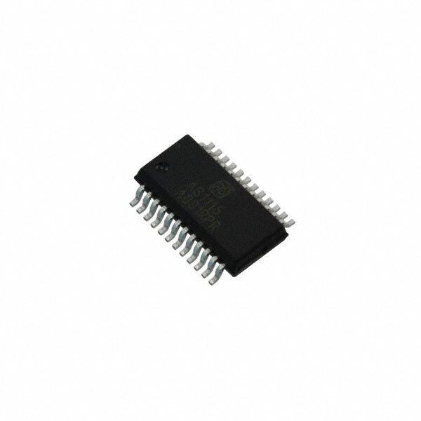
| 描述 | IC LCD DRV UNVRSL LOW-MUX 56VSOP |
| 产品分类 | |
| 品牌 | NXP Semiconductors |
| 数据手册 | |
| 产品图片 |
|
| 产品型号 | PCF8576T/1,118 |
| PCN封装 | |
| rohs | 无铅 / 符合限制有害物质指令(RoHS)规范要求 |
| 产品系列 | - |
| 产品培训模块 | http://www.digikey.cn/PTM/IndividualPTM.page?site=cn&lang=zhs&ptm=17227 |
| 供应商器件封装 | 56-VSOP |
| 其它名称 | 568-8087-2 |
| 包装 | 带卷 (TR) |
| 安装类型 | 表面贴装 |
| 封装/外壳 | 56-BSOP(0.435",11.50mm 宽) |
| 工作温度 | -40°C ~ 85°C |
| 接口 | I²C,2 线串口 |
| 数字或字符 | 10 个字符, 20 个字符, 160 元件 |
| 显示类型 | LCD |
| 标准包装 | 500 |
| 电压-电源 | 2 V ~ 9 V |
| 电流-电源 | 180µA |
| 配置 | 8 段,15 段,160 元件 |


PDF Datasheet 数据手册内容提取
INTEGRATED CIRCUITS DATA SHEET PCF8576 Universal LCD driver for low multiplex rates Product specification 2001 Oct 02 Supersedes data of 1998 Feb 06 File under Integrated Circuits, IC12
Philips Semiconductors Product specification Universal LCD driver for low multiplex rates PCF8576 CONTENTS 8 LIMITING VALUES 9 HANDLING 1 FEATURES 10 DC CHARACTERISTICS 2 GENERAL DESCRIPTION 11 AC CHARACTERISTICS 3 ORDERING INFORMATION 11.1 Typical supply current characteristics 4 BLOCK DIAGRAM 11.2 Typical characteristics of LCD outputs 5 PINNING 12 APPLICATION INFORMATION 6 FUNCTIONAL DESCRIPTION 12.1 Chip-on-glass cascadability in single plane 6.1 Power-on reset 13 BONDING PAD INFORMATION 6.2 LCDbias generator 6.3 LCDvoltage selector 14 TRAY INFORMATION: PCF8576U 6.4 LCD drive mode waveforms 15 TRAY INFORMATION: PCF8576U/2 6.5 Oscillator 16 PACKAGE OUTLINES 6.5.1 Internal clock 17 SOLDERING 6.5.2 External clock 6.6 Timing 17.1 Introduction to soldering surface mount 6.7 Display latch packages 6.8 Shift register 17.2 Reflow soldering 6.9 Segment outputs 17.3 Wave soldering 6.10 Backplane outputs 17.4 Manual soldering 6.11 Display RAM 17.5 Suitability of surface mount IC packages for 6.12 Data pointer wave and reflow soldering methods 6.13 Subaddress counter 18 DATA SHEET STATUS 6.14 Output bank selector 19 DEFINITIONS 6.15 Input bank selector 6.16 Blinker 20 DISCLAIMERS 7 CHARACTERISTICS OF THE I2C-BUS 21 PURCHASE OF PHILIPS I2C COMPONENTS 7.1 Bit transfer (see Fig.12) 7.2 START and STOP conditions (see Fig.13) 7.3 System configuration (see Fig.14) 7.4 Acknowledge (see Fig.15) 7.5 PCF8576 I2C-bus controller 7.6 Input filters 7.7 I2C-bus protocol 7.8 Command decoder 7.9 Display controller 7.10 Cascaded operation 2001Oct02 2
Philips Semiconductors Product specification Universal LCD driver for low multiplex rates PCF8576 1 FEATURES • Single-chip LCD controller/driver • Selectablebackplanedriveconfiguration:staticor2/3/4 backplane multiplexing • Selectable display bias configuration: static,1⁄ or1⁄ 2 3 • Internal LCD bias generation with voltage-follower • May be cascaded for large LCD applications (up to buffers 2560segments possible) • 40segment drives: up to twenty 8-segment numeric • Cascadable with 24-segment LCD driver PCF8566 characters; up to ten 15-segment alphanumeric • Optimized pinning for plane wiring in both single and characters; or any graphics of up to 160elements multiple PCF8576 applications • 40· 4-bit RAM for display data storage • Space-saving56-leadplasticverysmalloutlinepackage • Auto-incremented display data loading across device (VSO56) subaddress boundaries • Very low external component count (at most one • Display memory bank switching in static and duplex resistor, even in multiple device applications) drive modes • Compatible with chip-on-glass technology • Versatile blinking modes • Manufactured in silicon gate CMOS process. • LCD and logic supplies may be separated • Wide power supply range: from 2V for low-threshold 2 GENERAL DESCRIPTION LCDs and up to 9V for guest-host LCDs and high-threshold (automobile) twisted nematic LCDs The PCF8576 is a peripheral device which interfaces to • Low power consumption almostanyLiquidCrystalDisplay(LCD)withlowmultiplex rates. It generates the drive signals for any static or • Power-saving mode for extremely low power multiplexedLCDcontaininguptofourbackplanesandup consumption in battery-operated and telephone to40segmentsandcaneasilybecascadedforlargerLCD applications applications. The PCF8576 is compatible with most • I2C-bus interface microprocessors/microcontrollersandcommunicatesviaa • TTL/CMOS compatible two-line bidirectional I2C-bus. Communication overheads are minimized by a display RAM with auto-incremented • Compatible with any 4-bit, 8-bit or 16-bit addressing, by hardware subaddressing and by display microprocessors/microcontrollers memory switching (static and duplex drive modes). 3 ORDERING INFORMATION PACKAGE TYPE NUMBER NAME DESCRIPTION VERSION PCF8576T VSO56 plastic very small outline package; 56leads SOT190-1 PCF8576U - chip in tray - PCF8576U/2 - chip with bumps in tray - PCF8576U/5 - unsawn wafer - PCF8576U/10 FFC chip on film frame carrier (FFC) - PCF8576U/12 FFC chip with bumps on film frame carrier (FFC) - 2001Oct02 3
This text is here in white to force landscape pages to be rotated correctly when browsing through the pdf in the Acrobat reader.This text is here in _whitetoforcelandscapepagestoberotatedcorrectlywhenbrowsingthroughthepdfintheAcrobatreader.ThistextishereinThistextisherein whitetoforcelandscapepagestoberotatedcorrectlywhenbrowsingthroughthepdfintheAcrobatreader.whitetoforcelandscapepagestobe... 2 4 P 0 h 01 B U ilip O L n s c O iv S t02 CK er em DIAG salL icondu BP0 BP2 BP1 BP3 S0 to S39 R c A C to 40 M D rs 13 14 15 16 17 to 56 d 5 r VDD BACKPLANE DISPLAY SEGMENT OUTPUTS iv OUTPUTS e R r f o r LCD DISPLAY LATCH lo R VOLTAGE w SELECTOR m u R LCD BIAS SHIFT REGISTER lti 12 GENERATOR p VLCD le x 4 4 PCF8576 r CLK INPUT DISPLAY OUTPUT a 3 TIMING BLINKER BANK RAM BANK t SYNC SELECTOR 40 x 4 BITS SELECTOR es DISPLAY CONTROLLER 6 OSC OSCILLATOR POWER- DATA ON POINTER RESET 11 COMMAND VSS DECODER 2 SUB- SCL INPUT I 2 C - BUS ADDRESS SDA 1 FILTERS CONTROLLER COUNTER 10 7 8 9 SA0 A0 A1 A2 P r pagewidth MBK276 PCF oduct sp Fig.1 Block diagram (for VSandbook, full O56 package; SOT190-1). 8576 ecificatio h n
Philips Semiconductors Product specification Universal LCD driver for low multiplex rates PCF8576 5 PINNING SYMBOL PIN DESCRIPTION SDA 1 I2C-bus serial data input/output SCL 2 I2C-bus serial clock input SYNC 3 cascade synchronization input/output CLK 4 external clock input/output V 5 supply voltage DD OSC 6 oscillator input A0toA2 7to9 I2C-bus subaddress inputs SA0 10 I2C-bus slave address input; bit0 V 11 logic ground SS V 12 LCD supply voltage LCD BP0,BP2,BP1andBP3 13to16 LCD backplane outputs S0toS39 17to56 LCD segment outputs 2001Oct02 5
Philips Semiconductors Product specification Universal LCD driver for low multiplex rates PCF8576 handbook, halfpage SDA 1 56 S39 SCL 2 55 S38 SYNC 3 54 S37 CLK 4 53 S36 VDD 5 52 S35 OSC 6 51 S34 A0 7 50 S33 A1 8 49 S32 A2 9 48 S31 SA0 10 47 S30 VSS 11 46 S29 VLCD 12 45 S28 BP0 13 44 S27 BP2 14 43 S26 PCF8576T BP1 15 42 S25 BP3 16 41 S24 S0 17 40 S23 S1 18 39 S22 S2 19 38 S21 S3 20 37 S20 S4 21 36 S19 S5 22 35 S18 S6 23 34 S17 S7 24 33 S16 S8 25 32 S15 S9 26 31 S14 S10 27 30 S13 S11 28 29 S12 MBK278 Fig.2 Pin configuration; SOT190-1. 2001Oct02 6
Philips Semiconductors Product specification Universal LCD driver for low multiplex rates PCF8576 6 FUNCTIONAL DESCRIPTION The host microprocessor/microcontroller maintains the 2-lineI2C-buscommunicationchannelwiththePCF8576. ThePCF8576isaversatileperipheraldevicedesignedto The internal oscillator is selected by connecting pinOSC interface to any microprocessor/microcontroller to a wide to pinV . The appropriate biasing voltages for the variety of LCDs. It can directly drive any static or SS multiplexedLCDwaveformsaregeneratedinternally.The multiplexedLCDcontaininguptofourbackplanesandup only other connections required to complete the system to 40segments. The display configurations possible with are to the power supplies (V , V and V ) and the the PCF8576 depend on the number of active backplane DD SS LCD LCD panel chosen for the application. outputs required; a selection of display configurations is given in Table. All of the display configurations given in Table can be implemented in the typical system shown in Fig.3. Selection of display configurations 14-SEGMENTS NUMBER OF 7-SEGMENTS NUMERIC ALPHANUMERIC DOT MATRIX INDICATOR INDICATOR BACKPLANES SEGMENTS DIGITS CHARACTERS SYMBOLS SYMBOLS 4 160 20 20 10 20 160dots (4· 40) 3 120 15 15 8 8 120dots (3· 40) 2 80 10 10 5 10 80dots (2· 40) 1 40 5 5 2 12 40dots (1· 40) handbook, full pagewidth V DD R tr 2CB V V DD LCD 5 12 SDA HOST 1 17 to 56 40 segment drives LCD PANEL MICRO- SCL PROCESSOR/ 2 PCF8576 (up to 160 MICRO- OSC elements) CONTROLLER 6 13 to 16 4 backplanes 7 8 9 10 11 ROSC A0 A1 A2 SA0 VSS MBK277 V SS Fig.3 Typical system configuration. 2001Oct02 7
Philips Semiconductors Product specification Universal LCD driver for low multiplex rates PCF8576 6.1 Power-on reset 6.3 LCDvoltage selector Atpower-onthePCF8576resetstoastartingconditionas TheLCDvoltageselectorco-ordinatesthemultiplexingof follows: the LCD in accordance with the selected LCD drive configuration. The operation of the voltage selector is 1. All backplane outputs are set to V . DD controlled by MODE SET commands from the command 2. All segment outputs are set to V . DD decoder. The biasing configurations that apply to the 3. Thedrivemode‘1:4multiplexwith1⁄3bias’isselected. preferred modes of operation, together with the biasing 4. Blinking is switched off. characteristics as functions of Vop=VDD- VLCD and the resulting discrimination ratios (D), are given in Table1. 5. Input and output bank selectors are reset (as defined in Table4). ApracticalvalueforV isdeterminedbyequatingV op off(rms) 6. The I2C-bus interface is initialized. withadefinedLCDthresholdvoltage(Vth),typicallywhen theLCDexhibitsapproximately10%contrast.Inthestatic 7. The data pointer and the subaddress counter are drive mode a suitable choice is V >3V approximately. op th cleared. Multiplex drive ratios of 1:3 and 1:4 with1⁄ bias are DatatransfersontheI2C-busshouldbeavoidedfor1ms 2 possible but the discrimination and hence the contrast followingpower-ontoallowcompletionoftheresetaction. ratios are smaller ( 3 =1.732 for 1:3 multiplex or 6.2 LCDbias generator 21 ---------- =1.528 for 1:4 multiplex). The full-scale LCD voltage (V ) is obtained from 3 op VDD- VLCD. The LCD voltage may be temperature The advantage of these modes is a reduction of the LCD compensatedexternallythroughtheVLCDsupplytopin12. full-scale voltage Vop as follows: Fractional LCD biasing voltages are obtained from an • 1:3 multiplex (1⁄ bias): internal voltage divider of the three series resistors 2 connectedbetweenV andV .Thecentreresistorcan V = 6· V =2.449V DD LCD op offÆ rmsæ off(rms) be switched out of the circuit to provide a1⁄ bias voltage 2 • 1:4 multiplex (1⁄ bias): level for the 1:2multiplex configuration. 2 V = (4· 3) =2.309V op ---------------------- off(rms) 3 ThesecomparewithV =3V when1⁄ biasisused. op off(rms) 3 Table 1 Preferred LCD drive modes: summary of characteristics LCD DRIVE MODE NUMBER OF LCD BIAS V-----o---f-f--(-r--m----s---) V-----o---n--(--r--m----s---) D = -V----o---n--(--r--m----s---) CONFIGURATION V V V BACKPLANES LEVELS op op off(rms) static 1 2 static 0 1 ¥ 1:2 2 3 1⁄ 0.354 0.791 2.236 2 1:2 2 4 1⁄ 0.333 0.745 2.236 3 1:3 3 4 1⁄ 0.333 0.638 1.915 3 1:4 4 4 1⁄ 0.333 0.577 1.732 3 2001Oct02 8
Philips Semiconductors Product specification Universal LCD driver for low multiplex rates PCF8576 6.4 LCD drive mode waveforms WhenthreebackplanesareprovidedintheLCD,the1:3 multiplex drive mode applies, as shown in Fig.7. The static LCD drive mode is used when a single backplaneisprovidedintheLCD.Backplaneandsegment When four backplanes are provided in the LCD, the 1:4 drive waveforms for this mode are shown in Fig.4. multiplex drive mode applies, as shown in Fig.8. When two backplanes are provided in the LCD, the 1:2 multiplex mode applies. The PCF8576 allows use of 1⁄ bias or1⁄ bias in this mode as shown in Figs5and6. 2 3 Tframe VDD LCD segments BP0 VLCD state 1 state 2 VDD (on) (off) Sn VLCD VDD Sn 1 VLCD (a) waveforms at driver Vop state 1 0 Vop Vop state 2 0 Vop (b) resultant waveforms at LCD segment MBE539 V (t) = V (t)–V (t) state1 Sn BP0 V = V on(rms) op V (t) = V (t)–V (t) state2 Sn+1 BP0 V = 0 V off(rms) Fig.4 Static drive mode waveforms (V =V - V ). op DD LCD 2001Oct02 9
Philips Semiconductors Product specification Universal LCD driver for low multiplex rates PCF8576 Tframe VDD LCD segments BP0 (VDD VLCD)/2 VLCD state 1 VDD state 2 BP1 (VDD VLCD)/2 VLCD VDD Sn VLCD VDD Sn 1 VLCD (a) waveforms at driver Vop V o p /2 state 1 0 V o p /2 Vop Vop V o p /2 state 2 0 V o p /2 Vop (b) resultant waveforms MBE540 at LCD segment V (t) = V (t)–V (t) state1 Sn BP0 V = 0.791V on(rms) op V (t) = V (t)–V (t) state2 Sn BP1 V = 0.354V off(rms) op Fig.5 Waveforms for the 1:2 multiplex drive mode with1⁄ bias (V =V - V ). 2 op DD LCD 2001Oct02 10
Philips Semiconductors Product specification Universal LCD driver for low multiplex rates PCF8576 Tframe VDD LCD segments BP0 V D D Vo p /3 V D D 2Vo p /3 VLCD state 1 VDD state 2 BP1 V D D Vo p /3 V D D 2Vo p /3 VLCD VDD Sn V D D Vo p /3 V D D 2Vo p /3 VLCD VDD Sn 1 V D D Vo p /3 V D D 2Vo p /3 VLCD (a) waveforms at driver Vop 2V o p /3 Vo p /3 state 1 0 Vo p /3 2V o p /3 Vop Vop 2V o p /3 Vo p /3 state 2 0 Vo p /3 2V o p /3 Vop (b) resultant waveforms MBE541 at LCD segment V (t) = V (t)–V (t) state1 Sn BP0 V = 0.745V on(rms) op V (t) = V (t)–V (t) state2 Sn BP1 V = 0.333V off(rms) op Fig.6 Waveforms for the 1:2 multiplex drive mode with1⁄ bias (V =V - V ). 3 op DD LCD 2001Oct02 11
Philips Semiconductors Product specification Universal LCD driver for low multiplex rates PCF8576 Tframe VDD LCD segments V D D Vo p /3 BP0 V D D 2Vo p /3 VLCD state 1 VDD state 2 V D D Vo p /3 BP1 V D D 2Vo p /3 VLCD VDD V D D Vo p /3 BP2/S23 V D D 2Vo p /3 VLCD VDD Sn V D D Vo p /3 V D D 2Vo p /3 VLCD VDD Sn 1 V D D Vo p /3 V D D 2Vo p /3 VLCD VDD Sn 2 V D D Vo p /3 V D D 2Vo p /3 VLCD (a) waveforms at driver Vop 2V o p /3 Vo p /3 state 1 0 Vo p /3 2V o p /3 Vop Vop 2V o p /3 Vo p /3 state 2 0 Vo p /3 2V o p /3 Vop (b) resultant waveforms at LCD segment MBE542 V (t) = V (t)–V (t) state1 Sn BP0 V = 0.638V on(rms) op V (t) = V (t)–V (t) state2 Sn BP1 V = 0.333V off(rms) op Fig.7 Waveforms for the 1:3 multiplex drive mode (V =V - V ). op DD LCD 2001Oct02 12
Philips Semiconductors Product specification Universal LCD driver for low multiplex rates PCF8576 Tframe VDD LCD segments V D D Vo p /3 BP0 V D D 2Vo p /3 VLCD state 1 VDD state 2 V D D Vo p /3 BP1 V D D 2Vo p /3 VLCD VDD V D D Vo p /3 BP2 V D D 2Vo p /3 VLCD VDD BP3 V D D Vo p /3 V D D 2Vo p /3 VLCD VDD Sn V D D Vo p /3 V D D 2Vo p /3 VLCD VDD Sn 1 V D D Vo p /3 V D D 2Vo p /3 VLCD VDD Sn 2 V D D Vo p /3 V D D 2Vo p /3 VLCD VDD Sn 3 V D D Vo p /3 V D D 2Vo p /3 VLCD (a) waveforms at driver Vop 2V o p /3 V o p /3 state 1 0 V o p /3 2V o p /3 Vop Vop 2V o p /3 V o p /3 state 2 0 V (t) = V (t)–V (t) V o p /3 state1 Sn BP0 2V o p /3 Von(rms) = 0.577Vop Vop (b) resultant waveforms V (t) = V (t)–V (t) at LCD segment MBE543 state2 Sn BP1 V = 0.333V off(rms) op Fig.8 Waveforms for the 1:4 multiplex drive mode (V =V - V ). op DD LCD 2001Oct02 13
Philips Semiconductors Product specification Universal LCD driver for low multiplex rates PCF8576 6.5 Oscillator 6.6 Timing 6.5.1 INTERNALCLOCK ThetimingofthePCF8576organizestheinternaldataflow of the device. This includes the transfer of display data The internal logic and the LCD drive signals of the from the display RAM to the display segment outputs. In PCF8576aretimedeitherbytheinternaloscillatororfrom cascaded applications, the synchronization signalSYNC an external clock. When the internal oscillator is used, maintains the correct timing relationship between the pinOSCshouldbeconnectedtopinV .Inthisevent,the SS PCF8576s in the system. The timing also generates the output from pinCLK provides the clock signal for LCD frame frequency which it derives as an integer cascaded PCF8566s in the system. multiple of the clock frequency (seeTable2). The frame WhereresistorR toV ispresent,theinternaloscillator frequency is set by the MODESET commands when osc SS is selected. The relationship between the oscillator internal clock is used, or by the frequency applied to frequency on pinCLK (f ) and R is shown in Fig.9. pinCLK when external clock is used. clk osc TheratiobetweentheclockfrequencyandtheLCDframe frequency depends on the mode in which the device is operating.Inthepower-savingmodethereductionratiois 103 MBE531 six times smaller; this allows the clock frequency to be reduced by a factor of six. The reduced clock frequency resultsinasignificantreductioninpowerdissipation.The f clk (kHz) lowerclockfrequencyhasthedisadvantageofincreasing theresponsetimewhenlargeamountsofdisplaydataare transmitted on the I2C-bus. max When a device is unable to digest a display data byte 102 beforethenextonearrives,itholdstheSCLlineLOWuntil the first display data byte is stored. This slows down the transmission rate of the I2C-bus but no data loss occurs. min Table 2 LCD frame frequencies NOMINAL 10 FRAME FRAME 102 103 Rosc(kW) 104 PCF8576 MODE FREQUENCY FREQUENCY (Hz) fclk» Ł(cid:231)(cid:230) 3----.-4--R---·-o---s-1-c--0----7ł(cid:247)(cid:246)-- (kHz) Normal mode ---f--c---l-k---- 64 2880 f Fig.9 Oscillator frequency as a function of Rosc. Power-saving mode ----c--l-k--- 64 480 6.5.2 EXTERNALCLOCK 6.7 Display latch The condition for external clock is made by connecting The display latch holds the display data while the pinOSC to pinV ; pinCLK then becomes the external correspondingmultiplexsignalsaregenerated.Thereisa DD clock input. one-to-one relationship between the data in the display latch, the LCD segment outputs and one column of the The clock frequency (f ) determines the LCD frame clk display RAM. frequency and the maximum rate for data reception from the I2C-bus. To allow I2C-bus transmissions at their 6.8 Shift register maximumdatarateof100kHz,f shouldbechosentobe clk above 125kHz. The shift register serves to transfer display information from the display RAM to the display latch while previous A clock signal must always be supplied to the device; data is displayed. removing the clock may freeze the LCD in a DC state. 2001Oct02 14
Philips Semiconductors Product specification Universal LCD driver for low multiplex rates PCF8576 6.9 Segment outputs correspondence between the RAM addresses and the segmentoutputs,andbetweentheindividualbitsofaRAM The LCD drive section includes 40segment outputs word and the backplane outputs. The first RAM column pinsS0toS39 which should be connected directly to the correspondstothe40segmentsoperatedwithrespectto LCD. The segment output signals are generated in backplane BP0 (see Fig.10). In multiplexed LCD accordance with the multiplexed backplane signals and applications the segment data of the second, third and with data resident in the display latch. When less than fourth column of the display RAM are time-multiplexed 40segment outputs are required the unused segment with BP1, BP2 andBP3 respectively. outputs should be left open-circuit. When display data is transmitted to the PCF8576 the 6.10 Backplane outputs display bytes received are stored in the display RAM in accordance with the selected LCD drive mode. To The LCD drive section includes four backplane outputs illustrate the filling order, an example of a 7-segment BP0toBP3 which should be connected directly to the numericdisplayshowingalldrivemodesisgiveninFig.11; LCD. The backplane output signals are generated in the RAMfilling organization depicted applies equally to accordancewiththeselectedLCDdrivemode.Iflessthan other LCD types. four backplane outputs are required the unused outputs can be left open-circuit. In the 1:3 multiplex drive mode WithreferencetoFig.11,inthestaticdrivemodetheeight BP3 carries the same signal as BP1, therefore these two transmitteddatabitsareplacedinbit0ofeightsuccessive adjacent outputs can be connected together to give displayRAMaddresses.Inthe1:2multiplexdrivemode enhanced drive capabilities. In the 1:2 multiplex drive theeighttransmitteddatabitsareplacedinbits0and1of mode BP0andBP2, BP1andBP3 respectively carry the four successive display RAM addresses. In the 1:3 samesignalsandmayalsobepairedtoincreasethedrive multiplex drive mode these bits are placed in capabilities. In the static drive mode the same signal is bits0,1and2ofthreesuccessiveaddresses,withbit2of carried by all four backplane outputs and they can be the third address left unchanged. This last bit may, if connected in parallel for very high drive requirements. necessary, be controlled by an additional transfer to this address but care should be taken to avoid overriding 6.11 Display RAM adjacentdatabecausefullbytesarealwaystransmitted.In the 1:4 multiplex drive mode the eight transmitted data The display RAM is a static 40· 4-bit RAM which stores bits are placed in bits0,1,2and3 of two successive LCD data. A logic1 in the RAM bit-map indicates the on display RAM addresses. state of the corresponding LCD segment; similarly, a logic0 indicates the off state. There is a one-to-one display RAM addresses (rows) / segment outputs (S) 0 1 2 3 4 35 36 37 38 39 0 display RAM bits (columns) / 1 backplane outputs (BP) 2 3 MBE525 Fig.10 DisplayRAMbit-mapshowingdirectrelationshipbetweendisplayRAMaddressesandsegmentoutputs, and between bits in a RAMword and backplane outputs. 2001Oct02 15
Philips Semiconductors Product specification Universal LCD driver for low multiplex rates PCF8576 6.12 Data pointer 6.14 Output bank selector The addressing mechanism for the display RAM is ThisselectsoneofthefourbitsperdisplayRAMaddress realized using the data pointer. This allows the loading of for transfer to the display latch. The actual bit chosen anindividualdisplaydatabyte,oraseriesofdisplaydata depends on the particular LCD drive mode in operation bytes,intoanylocationofthedisplayRAM.Thesequence and on the instant in the multiplex sequence. In 1:4 commenceswiththeinitializationofthedatapointerbythe multiplex, all RAM addresses of bit0 are the first to be LOAD DATA POINTER command. Following this, an selected, these are followed by the contents of bit1,bit2 arriving data byte is stored starting at the display RAM and then bit3. Similarly in 1:3 multiplex, bits0,1and2 address indicated by the data pointer thereby observing are selected sequentially. In 1:2 multiplex, bits0and1 the filling order shown in Fig.11. The data pointer is are selected and, in the static mode, bit0 is selected. automaticallyincrementedinaccordancewiththechosen The PCF8576 includes a RAMbank switching feature in LCD configuration. That is, after each byte is stored, the the static and 1:2 multiplex drive modes. In the static contents of the data pointer are incremented by eight drive mode, the BANKSELECT command may request (staticdrivemode),byfour(1:2multiplexdrivemode)or the contents of bit2 to be selected for display instead of by two (1:4 multiplex drive mode). bit0 contents. In the 1:2 drive mode, the contents of bits2and3maybeselectedinsteadofbits0and1.This 6.13 Subaddress counter givestheprovisionforpreparingdisplayinformationinan Thestorageofdisplaydataisconditionedbythecontents alternative bank and to be able to switch to it once it is of the subaddress counter. Storage is allowed to take assembled. place only when the contents of the subaddress counter agree with the hardware subaddress applied to A0, A1 6.15 Input bank selector andA2. The subaddress counter value is defined by the Theinputbankselectorloadsdisplaydataintothedisplay DEVICESELECT command. If the contents of the RAM in accordance with the selected LCD drive subaddresscounterandthehardwaresubaddressdonot configuration.Displaydatacanbeloadedinbit2instatic agreethendatastorageisinhibitedbutthedatapointeris drive mode or in bits2and3 in 1:2 drive mode by using incremented as if data storage had taken place. The the BANKSELECT command. The input bank selector subaddress counter is also incremented when the data functions independent of the output bank selector. pointer overflows. The storage arrangements described lead to extremely efficient data loading in cascaded applications. When a series of display bytes are sent to the display RAM, automatic wrap-over to the next PCF8576 occurs when thelastRAMaddressisexceeded.Subaddressingacross deviceboundariesissuccessfulevenifthechangetothe next device in the cascade occurs within a transmitted character (such as during the 14thdisplay data byte transmitted in 1:3 multiplex mode). 2001Oct02 16
Philips Semiconductors Product specification Universal LCD driver for low multiplex rates PCF8576 6.16 Blinker bank selector, the displayed RAM banks are exchanged with alternate RAM banks at the blinking frequency. This The display blinking capabilities of the PCF8576 are very mode can also be specified by the BLINK command. versatile.Thewholedisplaycanbeblinkedatfrequencies selectedbytheBLINKcommand.Theblinkingfrequencies Inthe1:3and1:4multiplexmodes,wherenoalternate are integer multiples of the clock frequency; the ratios RAM bank is available, groups of LCD segments can be betweentheclockandblinkingfrequenciesdependonthe blinked by selectively changing the display RAM data at mode in which the device is operating, as shown in fixed time intervals. Table3. If the entire display is to be blinked at a frequency other An additional feature is for an arbitrary selection of LCD thanthenominalblinkingfrequency,thiscanbeeffectively segments to be blinked. This applies to the static and performedbyresettingandsettingthedisplayenablebitE 1:2LCD drive modes and can be implemented without at the required rate using the MODESET command. any communication overheads. By means of the output Table 3 Blinking frequencies NORMAL OPERATING POWER-SAVING MODE NOMINAL BLINKING BLINKING MODE MODE RATIO RATIO FREQUENCY Off - - blinking off f f 2Hz -------c--l-k------ -------c--l-k------ 2Hz 92160 15360 f f 1Hz ---------c--l-k-------- -------c--l-k------ 1Hz 184320 30720 f f 0.5Hz ---------c--l-k-------- -------c--l-k------ 0.5Hz 368640 61440 2001Oct02 17
This text is here in white to force landscape pages to be rotated correctly when browsing through the pdf in the Acrobat reader.This text is here in _whitetoforcelandscapepagestoberotatedcorrectlywhenbrowsingthroughthepdfintheAcrobatreader.ThistextishereinThistextisherein whitetoforcelandscapepagestoberotatedcorrectlywhenbrowsingthroughthepdfintheAcrobatreader.whitetoforcelandscapepagestobe... 2 P 0 h 01 U ilip O n s c iv S t0 e em 2 drive mode LCD segments LCD backplanes display RAM filling order transmitted display byte r s ic a o n l d a L u SSnn 32 f b Sn 1 BP0 n n 1 n 2 n 3 n 4 n 5 n 6 n 7 MSB LSB CD ctors static SSnn 54 e g c SSnn 7 bBiPt/ 012 cxx bxx axx fxx gxx exx dxx DxxP c b a f g e d DP driv d DP 3 x x x x x x x x e Sn 6 r f o BP0 r Sn a n n 1 n 2 n 3 lo 1 : 2 Sn 1 f b MSB LSB w bit/ 0 a f e d m g BP1 BP 1 b g c DP a b f g e c d DP u multiplex Sn 2 e c 2 x x x x lt 3 x x x x ip d DP Sn 3 le x 1 BP0 8 Sn 1 a n n 1 n 2 ra 1 : 3 Sn 2 f b Sn te bit/ 0 b a f MSB LSB s g BP 1 DP d e multiplex e BP1 BP2 2 c g x b DP c a d g f e c 3 x x x d DP Sn a n n 1 1 : 4 f b BP0 BP2 bit/ 0 a f g BP 1 c e MSB LSB multiplex e c BP1 BP3 2 b g a c b DP f e g d 3 DP d Sn 1 d DP P r width MBK389 P odu ge C c ull pa F t sp x=data biFt uignc.h1a1n g eRde.lationships between LCD layout, drive mode, dhandbook, fisplay RAM filling order and display data transmitted over the I2C-bus. 8576 ecificatio n
Philips Semiconductors Product specification Universal LCD driver for low multiplex rates PCF8576 7 CHARACTERISTICS OF THE I2C-BUS 7.5 PCF8576 I2C-bus controller The I2C-bus is for bidirectional, two-line communication The PCF8576 acts as an I2C-bus slave receiver. It does between different ICs or modules. The two lines are a notinitiateI2C-bustransfersortransmitdatatoanI2C-bus serial data line (SDA) and a serial clock line (SCL). Both master receiver. The only data output from the PCF8576 linesmustbeconnectedtoapositivesupplyviaapull-up are the acknowledge signals of the selected devices. resistorwhenconnectedtotheoutputstagesofadevice. Device selection depends on the I2C-bus slave address, Data transfer may be initiated only when the bus is not on the transferred command data and on the hardware busy. subaddress. In single device application, the hardware subaddress 7.1 Bit transfer(see Fig.12) inputsA0,A1andA2arenormallyconnectedtoV which SS One data bit is transferred during each clock pulse. The defines the hardware subaddress0. In multiple device dataontheSDAlinemustremainstableduringtheHIGH applicationsA0,A1andA2areconnectedtoV orV in SS DD periodoftheclockpulseaschangesinthedatalineatthis accordancewithabinarycodingschemesuchthatnotwo time will be interpreted as a control signal. devices with a common I2C-bus slave address have the same hardware subaddress. 7.2 START and STOP conditions(see Fig.13) Inthepower-savingmodeitispossiblethatthePCF8576 BothdataandclocklinesremainHIGHwhenthebusisnot is not able to keep up with the highest transmission rates busy.AHIGH-to-LOWtransitionofthedataline,whilethe whenlargeamountsofdisplaydataaretransmitted.Ifthis clock is HIGH is defined as the START condition (S). A situationoccurs,thePCF8576forcestheSCLlinetoLOW LOW-to-HIGHtransitionofthedatalinewhiletheclockis until its internal operations are completed. This is known HIGH is defined as the STOP condition (P). as the ‘clock synchronization feature’ of the I2C-bus and servestoslowdownfasttransmitters.Datalossdoesnot 7.3 System configuration(see Fig.14) occur. Adevicegeneratingamessageisa‘transmitter’,adevice 7.6 Input filters receiving a message is the ‘receiver’. The device that controlsthemessageisthe‘master’andthedeviceswhich To enhance noise immunity in electrically adverse are controlled by the master are the ‘slaves’. environments, RC low-pass filters are provided on the SDA and SCL lines. 7.4 Acknowledge(see Fig.15) 7.7 I2C-bus protocol ThenumberofdatabytestransferredbetweentheSTART and STOP conditions from transmitter to receiver is TwoI2C-busslaveaddresses(0111000and0111001)are unlimited. Each byte of eight bits is followed by an reserved for the PCF8576. The least significant bit of the acknowledge bit. The acknowledge bit is a HIGH level slaveaddressthataPCF8576willrespondtoisdefinedby signalputonthebusbythetransmitterduringwhichtime the level connected at its input pinSA0. Therefore, two themastergeneratesanextraacknowledgerelatedclock types of PCF8576 can be distinguished on the same pulse.Aslavereceiverwhichisaddressedmustgenerate I2C-bus which allows: an acknowledge after the reception of each byte. Also a • Upto16PCF8576sonthesameI2C-busforverylarge master receiver must generate an acknowledge after the LCD applications reception of each byte that has been clocked out of the • The use of two types of LCD multiplex on the same slave transmitter. The device that acknowledges must I2C-bus. pull-down the SDA line during the acknowledge clock pulse,sothattheSDAlineisstableLOWduringtheHIGH TheI2C-busprotocolisshowninFig.16.Thesequenceis periodoftheacknowledgerelatedclockpulse(set-upand initiated with a START condition (S) from the I2C-bus hold times must be taken into consideration). A master masterwhichisfollowedbyoneofthetwoPCF8576slave receiver must signal an end of data to the transmitter by addressesavailable.AllPCF8576swiththecorresponding not generating an acknowledge on the last byte that has SA0 level acknowledge in parallel with the slave address beenclockedoutoftheslave.Inthiseventthetransmitter butallPCF8576swiththealternativeSA0levelignorethe must leave the data line HIGH to enable the master to whole I2C-bus transfer. generate a STOP condition. 2001Oct02 19
Philips Semiconductors Product specification Universal LCD driver for low multiplex rates PCF8576 Afteracknowledgement,oneormorecommandbytes(m) 7.8 Command decoder followwhichdefinethestatusoftheaddressedPCF8576s. The command decoder identifies command bytes that The last command byte is tagged with a cleared most arrive on the I2C-bus. All available commands carry a significantbit,thecontinuationbitC.Thecommandbytes continuation bitC in their most significant bit position arealsoacknowledgedbyalladdressedPCF8576sonthe (Fig.17).Whenthisbitisset,itindicatesthatthenextbyte bus. of the transfer to arrive will also represent a command. If this bit is reset, it indicates the last command byte of the Afterthelastcommandbyte,aseriesofdisplaydatabytes transfer. Further bytes will be regarded as display data. (n) may follow. These display bytes are stored in the display RAM at the address specified by the data pointer ThefivecommandsavailabletothePCF8576aredefined and the subaddress counter. Both data pointer and in Table4. subaddress counter are automatically updated and the data is directed to the intended PCF8576 device. The acknowledgementaftereachbyteismadeonlybythe(A0, A1 and A2) addressed PCF8576. After the last display byte, the I2C-bus master issues a STOP condition(P). SDA SCL data line change stable; of data data valid allowed MBA607 Fig.12 Bit transfer. handbook, full pagewidth SDA SDA SCL SCL S P START condition STOP condition MBC622 Fig.13 Definition of START and STOP conditions. 2001Oct02 20
Philips Semiconductors Product specification Universal LCD driver for low multiplex rates PCF8576 MASTER SLAVE MASTER SLAVE MASTER TRANSMITTER/ TRANSMITTER/ TRANSMITTER/ RECEIVER TRANSMITTER RECEIVER RECEIVER RECEIVER SDA SCL MGA807 Fig.14 System configuration. handbook, full pagewidth DATA OUTPUT BY TRANSMITTER not acknowledge DATA OUTPUT BY RECEIVER acknowledge SCL FROM 1 2 8 9 MASTER S clock pulse for START acknowledgement condition MBC602 Fig.15 Acknowledgement on the I2C-bus. 2001Oct02 21
Philips Semiconductors Product specification Universal LCD driver for low multiplex rates PCF8576 handbook, full pagewidth acaklln aodwdlreedsgsee dby bya Ac0kn, oAw1 leadngde A2 R/W PCF8576s selected PCF8576 only slave address S S 0 1 1 1 0 0 A 0 A C COMMAND A DISPLAY DATA A P 0 1 byte n 1 byte(s) n 0 byte(s) update data pointers and if necessary, MBK279 subaddress counter Fig.16 I2C-bus protocol. MSB LSB C REST OF OPCODE MSA833 C=0; last command. C=1; commands continue. Fig.17 General format of command byte. 2001Oct02 22
Philips Semiconductors Product specification Universal LCD driver for low multiplex rates PCF8576 Table 4 Definition of PCF8576 commands COMMAND OPCODE OPTIONS DESCRIPTION MODE SET C 1 0 LP E B M1 M0 Table5 Defines LCD drive mode. Table6 Defines LCD bias configuration. Table7 Defines display status. The possibility to disable the display allows implementation of blinking under external control. Table8 Defines power dissipation mode. LOADDATA C 0 P5 P4 P3 P2 P1 P0 Table9 Sixbits of immediate data, bits P5toP0, are POINTER transferred to the data pointer to define one of forty display RAM addresses. DEVICE C 1 1 0 0 A2 A1 A0 Table10 Threebits of immediate data, bitsA2toA0, are SELECT transferredtothesubaddresscountertodefineoneof eight hardware subaddresses. BANK C 1 1 1 1 0 I O Table11 Defines input bank selection (storage of arriving SELECT display data). Table12 Definesoutputbankselection(retrievalofLCDdisplay data). The BANK SELECT command has no effect in 1:3 and 1:4 multiplex drive modes. BLINK C 1 1 1 0 A BF1 BF0 Table13 Defines the blinking frequency. Table14 Selects the blinking mode; normal operation with frequencysetbyBF1,BF0orblinkingbyalternationof display RAM banks. Alternation blinking does not apply in 1:3 and 1:4 multiplex drive modes. Table 5 MODE SET option1 Table 8 MODE SET option4 LCD DRIVE MODE BITS MODE BITLP DRIVE MODE BACKPLANE M1 M0 Normal mode 0 Power-saving mode 1 Static 1BP 0 1 1:2 MUX (2BP) 1 0 Table 9 LOAD DATA POINTER option1 1:3 MUX (3BP) 1 1 DESCRIPTION BITS 1:4 MUX (4BP) 0 0 6-bitbinaryvalueof0to39 P5 P4 P3 P2 P1 P0 Table 6 MODE SET option2 Table 10 DEVICE SELECT option1 LCD BIAS BITB 1⁄ bias 0 DESCRIPTION BITS 3 1⁄ bias 1 3-bit binary value of 0to7 A2 A1 A0 2 Table 7 MODE SET option3 Table 11 BANK SELECT option1 DISPLAY STATUS BITE STATIC 1:2 MUX BITI Disabled (blank) 0 RAM bit0 RAM bits0 and1 0 Enabled 1 RAM bit2 RAM bits2 and3 1 2001Oct02 23
Philips Semiconductors Product specification Universal LCD driver for low multiplex rates PCF8576 Table 12 BANK SELECT option2 7.10 Cascaded operation STATIC 1:2 MUX BITO Inlargedisplayconfigurations,upto16PCF8576scanbe distinguished on the same I2C-bus by using the 3-bit RAM bit0 RAM bits0 and1 0 hardware subaddress (A0, A1 and A2) and the RAM bit2 RAM bits2 and3 1 programmable I2C-bus slave address (SA0). When cascaded PCF8576s are synchronized so that they can Table 13 BLINK option1 sharethebackplanesignalsfromoneofthedevicesinthe cascade. Such an arrangement is cost-effective in large BITS BLINK FREQUENCY LCDapplicationssincethebackplaneoutputsofonlyone BF1 BF0 device need to be through-plated to the backplane electrodes of the display. The other PCF8576s of the Off 0 0 cascade contribute additional segment outputs but their 2Hz 0 1 backplane outputs are left open-circuit (see Fig.18). 1Hz 1 0 TheSYNC line is provided to maintain the correct 0.5Hz 1 1 synchronization between all cascaded PCF8576s. This synchronization is guaranteed after the Power-on reset. Table 14 BLINK option2 The only time thatSYNC is likely to be needed is if synchronization is accidentally lost (e.g. by noise in BLINK MODE BITA adverse electrical environments; or by the definition of a Normal blinking 0 multiplexmodewhenPCF8576swithdifferingSA0levels Alternation blinking 1 arecascaded).SYNCisorganizedasaninput/outputpin; theoutputselectionbeingrealizedasanopen-draindriver 7.9 Display controller with an internal pull-up resistor. A PCF8576 asserts the SYNC line at the onset of its last active backplane signal The display controller executes the commands identified and monitors theSYNC line at all other times. Should by the command decoder. It contains the status registers synchronization in the cascade be lost, it will be restored of the PCF8576 and co-ordinates their effects. The by the first PCF8576 to assertSYNC. The timing controller is also responsible for loading display data into relationship between the backplane waveforms and the the display RAM as required by the filling order. SYNCsignalforthevariousdrivemodesofthePCF8576 are shown in Fig.19. For single plane wiring of packaged PCF8576s and chip-on-glass cascading, see Chapter12. 2001Oct02 24
Philips Semiconductors Product specification Universal LCD driver for low multiplex rates PCF8576 handbook, full pagewidth VDD VLCD SDA 1 5 12 SCL 2 17 to 56 40 segment drives LCD PANEL SYNC 3 PCF8576 CLK 4 13, 15 (up to 2560 OSC 14, 16 elements) 6 BP0 to BP3 7 8 9 10 11 (open-circuit) A0 A1 A2 SA0 VSS V LCD VDD R tr 2CB VDD VLCD 5 12 SDA HOST 1 17 to 56 40 segment drives MICRO- SCL 2 PROCESSOR/ PCF8576 SYNC MICRO- 3 CONTROLLER CLK 13, 15 4 backplanes 4 14, 16 OSC BP0 to BP3 6 MBK280 7 8 9 10 11 A0 A1 A2 SA0 V VSS SS Fig.18 Cascaded PCF8576 configuration. 2001Oct02 25
Philips Semiconductors Product specification Universal LCD driver for low multiplex rates PCF8576 1 handbook, full pagewidth T = f frame frame BP0 SYNC (a) static drive mode. BP1 (1/2 bias) BP1 (1/3 bias) SYNC (b) 1 : 2 multiplex drive mode. BP2 SYNC (c) 1 : 3 multiplex drive mode. BP3 SYNC MBE535 (d) 1 : 4 multiplex drive mode. ExcessivecapacitivecouplingbetweenSCLorCLKandSYNCmaycauseerroneoussynchronization.Ifthisprovestobeaproblem,thecapacitance oftheSYNClineshouldbeincreased(e.g.byanexternalcapacitorbetweenSYNCandVDD).DegradationofthepositiveedgeoftheSYNCpulsemay be countered by an external pull-up resistor. Fig.19 Synchronization of the cascade for the various PCF8576 drive modes. 2001Oct02 26
Philips Semiconductors Product specification Universal LCD driver for low multiplex rates PCF8576 8 LIMITING VALUES In accordance with the Absolute Maximum Rating System (IEC60134). SYMBOL PARAMETER MIN. MAX. UNIT V supply voltage - 0.5 +11.0 V DD V LCD supply voltage V - 11.0 V V LCD DD DD V input voltage SDA, SCL, CLK,SYNC, SA0, OSC, A0toA2 V - 0.5 V +0.5 V I SS DD V output voltage S0toS39, BP0toBP3 V - 0.5 V +0.5 V O LCD DD I DC input current - 20 mA I I DC output current - 25 mA O I , I , I V , V or V current - 50 mA DD SS LCD DD SS LCD P total power dissipation - 400 mW tot P power dissipation per output - 100 mW O T storage temperature - 65 +150 (cid:176) C stg 9 HANDLING Inputs and outputs are protected against electrostatic discharge in normal handling. However, to be totally safe, it is desirable to take normal precautions appropriate to handling MOSdevices (see“Handling MOS Devices”). 2001Oct02 27
Philips Semiconductors Product specification Universal LCD driver for low multiplex rates PCF8576 10 DC CHARACTERISTICS V =2to9V; V =0V; V =V - 2VtoV - 9V; T =- 40to+85(cid:176) C; unless otherwise specified. DD SS LCD DD DD amb SYMBOL PARAMETER CONDITIONS MIN. TYP. MAX. UNIT Supplies V supply voltage 2 - 9 V DD V LCD supply voltage note1 V - 9 - V - 2 V LCD DD DD I supply current note2 DD normal mode f =200kHz - - 180 m A clk power-saving mode f =35kHz; V =3.5V; - - 60 m A clk DD V =0V; A0,A1andA2 LCD connected to V SS Logic V LOW-level input voltage V - 0.3V V IL SS DD V HIGH-level input voltage 0.7V - V V IH DD DD V LOW-level output voltage I =0mA - - 0.05 V OL OL V HIGH-level output voltage I =0mA V - 0.05 - - V OH OH DD I LOW-level output current V =1V; V =5V 1 - - mA OL1 OL DD CLK,SYNC I HIGH-level output current CLK V =4V; V =5V 1 - - mA OH1 OH DD I LOW-level output current V =0.4V; V =5V 3 - - mA OL2 OL DD SDAandSCL I leakage current SA0,A0toA2, V =V or V - - 1 m A L1 I DD SS CLK, SDAandSCL I leakage current OSC V =V - - 1 m A L2 I DD I A0,A1,A2andOSC pull-down V =1V; V =5V 20 50 150 m A pd I DD current R pull-up resistor (SYNC) 20 50 150 kW SYNC V Power-on reset voltage level note3 - 1.0 1.6 V POR C input capacitance note4 - - 7 pF I LCD outputs V DC voltage component BP0toBP3 C =35nF - 20 - mV BP BP V DC voltage component S0toS39 C =5nF - 20 - mV S S R output resistance BP0toBP3 note5; V =V - 5V - - 5 kW BP LCD DD R output resistance S0toS39 note5; V =V - 5V - - 7.5 kW S LCD DD Notes 1. V £ V - 3V for1⁄ bias. LCD DD 3 2. LCD outputs are open-circuit; inputs at V or V ; external clock with 50%duty factor; I2C-bus inactive. SS DD 3. Resets all logic when V <V . DD POR 4. Periodically sampled, not 100%tested. 5. Outputs measured one at a time. 2001Oct02 28
Philips Semiconductors Product specification Universal LCD driver for low multiplex rates PCF8576 11 AC CHARACTERISTICS V =2to9V; V =0V; V =V - 2VtoV - 9V; T =- 40to+85(cid:176) C; unless otherwise specified. DD SS LCD DD DD amb SYMBOL PARAMETER CONDITIONS MIN. TYP. MAX. UNIT f oscillator frequency on pinCLK clk normal mode V =5V; note1 125 200 288 kHz DD power-saving mode V =3.5V 21 31 48 kHz DD t CLK HIGH time seeFig.21 1 - - m s clkH t CLK LOW time 1 - - m s clkL t SYNC propagation delay time - - 400 ns PSYNC t SYNC LOW time 1 - - m s SYNCL t driver delays with test loads V =V - 5V; seeFig.20 - - 30 m s PLCD LCD DD Timing characteristics: I2C-bus; note2; seeFig.22 t tolerable spike width on bus - - 100 ns SW t bus free time 4.7 - - m s BUF t START condition hold time 4.0 - - m s HD;STA t set-up time for a repeated START condition 4.7 - - m s SU;STA t SCL LOW time 4.7 - - m s LOW t SCL HIGH time 4.0 - - m s HIGH t SCL and SDA rise time - - 1 m s r t SCL and SDA fall time - - 0.3 m s f C capacitive bus line load - - 400 pF B t data set-up time 250 - - ns SU;DAT t data hold time 0 - - ns HD;DAT t set-up time for STOP condition 4.0 - - m s SU;STO Notes 1. At f <125kHz, I2C-bus maximum transmission speed is derated. clk 2. Alltimingvaluesarevalidwithintheoperatingsupplyvoltageandambienttemperaturerangeandarereferencedto V and V with an input voltage swing of V toV . IL IH SS DD 6.8W SYNC VDD (2%) CLK 3.3 kW 0.5VDD SSDCAL, 1.5 kW VDD (2%) (2%) BP0 to BP3, and 1 nF S0 to S39 VDD MBE544 Fig.20 Test loads. 2001Oct02 29
Philips Semiconductors Product specification Universal LCD driver for low multiplex rates PCF8576 handbook, full pagewidth 1/ fclk tclkH tclkL 0.7VDD CLK 0.3VDD 0.7VDD SYNC 0.3VDD t t PSYNC PSYNC t SYNCL 0.5 V BP0 to BP3, and S0 to S39 (VDD = 5 V) 0.5 V tPLCD MBE545 Fig.21 Driver timing waveforms. handbook, full pagewidth SDA tBUF tLOW tf SCL tHD;STA tr tHD;DAT tHIGH tSU;DAT SDA tSU;STA MGA728 tSU;STO Fig.22 I2C-bus timing waveforms. 2001Oct02 30
Philips Semiconductors Product specification Universal LCD driver for low multiplex rates PCF8576 11.1 Typical supply current characteristics MBE530 MBE529 50 50 ISS ILCD (m A) normal (m A) 40 mode 40 30 30 20 20 power-saving mode 10 10 0 0 0 100 fframe(Hz) 200 0 100 fframe(Hz) 200 VDD=5V; VLCD=0V; Tamb=25(cid:176)C. VDD=5V; VLCD=0V; Tamb=25(cid:176)C. Fig.23 - I as a function of f . Fig.24 - I as a function of f . SS frame LCD frame MBE528 - 1 MBE527 - 1 50 50 handbook, halfpage handbook, halfpage I I SS LCD (m A) (m A) 40 normal mode 40 f c lk = 200 kHz 85 o C 30 30 25 o C 20 20 power-saving mode 40 o C 10 f c l k = 35 kHz 10 0 0 0 5 V (V) 10 0 5 V (V) 10 DD DD VLCD=0V; external clock; Tamb=25(cid:176)C. VLCD=0V; external clock; fclk=nominal frequency. Fig.25 I as a function of V . Fig.26 I as a function of V . SS DD LCD DD 2001Oct02 31
Philips Semiconductors Product specification Universal LCD driver for low multiplex rates PCF8576 11.2 Typical characteristics of LCD outputs MBE532 - 1 MBE526 10 2.5 handbook, halfpage RO(max) RS R O(max) (kW) (kW) 2.0 RS 1.5 1 RBP RBP 1.0 0.5 10-1 0 0 3 6 40 0 40 80 120 VDD (V) T ( o C) amb VLCD=0V; Tamb=25(cid:176)C. VDD=5V; VLCD=0V. Fig.27 RO(max) as a function of VDD. Fig.28 RO(max) as a function of Tamb. 2001Oct02 32
This text is here in white to force landscape pages to be rotated correctly when browsing through the pdf in the Acrobat reader.This text is here in _whitetoforcelandscapepagestoberotatedcorrectlywhenbrowsingthroughthepdfintheAcrobatreader.ThistextishereinThistextisherein whitetoforcelandscapepagestoberotatedcorrectlywhenbrowsingthroughthepdfintheAcrobatreader.whitetoforcelandscapepagestobe... 2 an 1 P 001Oct02 dbook, full pagewidth SSVVCSYSDCDLNKSALDC 2APPLICATION UniversalL hilips Semicondu VLCD IN C cto F D rs SDA 1 56 S39 1 56 S79 O R d SCL 2 55 S38 2 55 S78 M r A iv SYNC 3 54 S37 3 54 S77 T e IO r CLK 4 53 S36 4 53 S76 N f o VDD 5 52 S35 5 52 S75 r OSC 6 51 S34 6 51 S74 lo w A0 7 50 S33 7 50 S73 m A1 8 49 S32 8 49 S72 u A2 9 48 S31 9 48 S71 l t i SA0 10 47 S30 10 47 S70 p l VSS 11 46 S29 11 46 S69 ex 3 3 VLCD 12 45 S28 12 45 S68 r a BP0 13 44 S27 BP0 13 44 S67 t e BP2 14 43 S26 BP2 14 43 S66 s PCF8576T open PCF8576T BP1 15 42 S25 BP1 15 42 S65 BP3 16 41 S24 BP3 16 41 S64 S0 17 40 S23 S40 17 40 S63 S1 18 39 S22 S41 18 39 S62 S2 19 38 S21 S42 19 38 S61 S3 20 S43 20 34 S17 34 S57 S7 24 33 S16 S47 24 33 S56 S8 25 32 S15 S48 25 32 S55 S9 26 31 S14 S49 26 31 S54 P S10 27 30 S13 S50 27 30 S53 r o S11 28 29 S12 S51 28 29 S52 P du C c S0 S10 S11 S12 S13 S39 S40 S50 S51 S52 S53 S79 F t sp 8 e backplanes segments MBK281 5 cifi Fig.29 Single plane wiring of packaged PCF8576Ts. 76 ca tio n
Philips Semiconductors Product specification Universal LCD driver for low multiplex rates PCF8576 12.1 Chip-on-glass cascadability in single plane andthebackplaneoutputpads.Theonlybuslinethatdoes not require a second opening to lead through to the next In chip-on-glass technology, where driver devices are PCF8576 is V , being the cascade centre. The placing bonded directly onto glass of the LCD, it is important that LCD of V adjacent to V allows the two supplies to be the devices may be cascaded without the crossing of LCD SS connected together. conductors,butthepathsofconductorscanbecontinued on the glass under the chip. All of this is facilitated by the Whenanexternalclockingsourceistobeused,OSCofall PCF8576bondingpadlayout(seeFig.30).Padsneeding devices should be connected to V . The padsOSC, DD businterconnectionbetweenallPCF8576softhecascade A0,A1,A2andSA0 have been placed between are V , V , V , CLK, SCL, SDA andSYNC. These V andV to facilitate wiring of oscillator, hardware DD SS LCD SS DD lines may be led to the corresponding pads of the next subaddress and slave address. PCF8576 through the wide opening between V pad LCD 13 BONDING PAD INFORMATION handbook, full pagewidth 17 16 15 14 13 12 11 10 9 8 7 6 5 4 S S S S S S S S S S S S S S 34 33 32 31 30 29 28 27 26 25 24 23 22 21 S18 35 20 S3 19 S2 S19 36 18 S1 S20 37 17 S0 S21 38 16 BP3 S22 39 15 BP1 S23 40 14 BP2 S24 41 13 BP0 S25 42 4.12 x mm 0 0 S26 43 S27 44 y S28 45 PCF8576 S29 46 S30 47 cascade centre 12 VLCD S31 48 11 VSS S32 49 10 SA0 S33 50 9 A2 51 52 53 54 55 56 1 2 3 4 5 6 7 8 4 5 6 7 8 9 A L C K D C 0 1 S3 S3 S3 S3 S3 S3 SD SC YN CL VD OS A A S 3.07 mm MBK282 Bonding pad dimensions: 120· 120m m. Gold bump dimensions: 94· 94· 25m m. Fig.30 Bonding pad locations. 2001Oct02 34
Philips Semiconductors Product specification Universal LCD driver for low multiplex rates PCF8576 Table 15 Bonding pad locations (dimensions in m m) COORDINATES All x and ycoordinates are referenced to centre of chip SYMBOL PAD (seeFig.30). x y S13 30 - 555 1900 COORDINATES SYMBOL PAD S14 31 - 755 1900 x y S15 32 - 955 1900 SDA 1 - 155 - 1900 S16 33 - 1155 1900 SCL 2 45 - 1900 S17 34 - 1375 1900 SYNC 3 245 - 1900 S18 35 - 1375 1660 CLK 4 445 - 1900 S19 36 - 1375 1420 V 5 645 - 1900 DD S20 37 - 1375 1200 OSC 6 865 - 1900 S21 38 - 1375 1000 A0 7 1105 - 1900 S22 39 - 1375 800 A1 8 1375 - 1900 S23 40 - 1375 600 A2 9 1375 - 1700 S24 41 - 1375 400 SA0 10 1375 - 1500 S25 42 - 1375 200 V 11 1375 - 1300 SS S26 43 - 1375 - 200 V 12 1375 - 1100 LCD S27 44 - 1375 - 400 BP0 13 1375 300 S28 45 - 1375 - 600 BP2 14 1375 500 S29 46 - 1375 - 800 BP1 15 1375 700 S30 47 - 1375 - 1000 BP3 16 1375 900 S31 48 - 1375 - 1200 S0 17 1375 1100 S32 49 - 1375 - 1420 S1 18 1375 1300 S33 50 - 1375 - 1660 S2 19 1375 1500 S34 51 - 1375 - 1900 S3 20 1375 1700 S35 52 - 1155 - 1900 S4 21 1375 1900 S36 53 - 955 - 1900 S5 22 1105 1900 S37 54 - 755 - 1900 S6 23 865 1900 S38 55 - 555 - 1900 S7 24 645 1900 S39 56 - 355 - 900 S8 25 445 1900 S9 26 245 1900 Table 16 Bonding pad dimensions S10 27 45 1900 Pad pitch 200m m S11 28 - 155 1900 Pad size, aluminium 120· 120m m S12 29 - 355 1900 Gold bump dimensions 94· 94· 25m m 2001Oct02 35
Philips Semiconductors Product specification Universal LCD driver for low multiplex rates PCF8576 14 TRAY INFORMATION: PCF8576U x handbook, full pagewidth G A C y H 1,1 2,1 x,1 D 1,2 B F 1,y x,y A A E M J SECTION A-A MGU431 For dimensions see Table18. Fig.31 Tray details. Table 17 Tray dimensions (see Fig.33) SYMBOL DESCRIPTION VALUE handbook, halfpage A pocket pitch;xdirection 6.32mm B pocket pitch;ydirection 6.32mm C pocket width;xdirection 4.55mm D pocket width;ydirection 4.55mm E tray width;xdirection 50.67mm F tray width;ydirection 50.67mm G cutcornertopocket1,1centre 6.32mm H cutcornertopocket1,1centre 6.32mm PC8576U J tray thickness 3.94mm M pocket depth 0.61mm x number of pockets;xdirection 7 MGU432 y number of pockets;ydirection 7 The orientation of theIC in a pocket is indicated by the positionoftheICtypenameonthediesurfacewithrespectto the chamfer on the upper left corner of the tray. Fig.32 Tray alignment. 2001Oct02 36
Philips Semiconductors Product specification Universal LCD driver for low multiplex rates PCF8576 15 TRAY INFORMATION: PCF8576U/2 handbook, full pagewidth x G A C y H 1,1 2,1 x,1 D 1,2 B F 1,y x,y A A E K M L J SECTION A-A MGW014 For dimensions see Table17. Fig.33 Tray details. Table 18 Tray dimensions (see Fig.31) SYMBOL DESCRIPTION VALUE handbook, halfpage A pocket pitch;xdirection 5.33mm B pocket pitch;ydirection 7.11mm C pocket width;xdirection 3.43mm D pocket width;ydirection 4.67mm E tray width;xdirection 50.67mm F tray width;ydirection 50.67mm G cutcornertopocket1,1centre 6.67mm H cutcornertopocket1,1centre 7.56mm J tray thickness 3.94mm PCF8576U/2 K tray cross section 1.76mm L tray cross section 2.46mm MGW015 M pocket depth 0.89mm x number of pockets;xdirection 8 The orientation of theIC in a pocket is indicated by the positionoftheICtypenameonthediesurfacewithrespectto y number of pockets;ydirection 6 the chamfer on the upper left corner of the tray. Fig.34 Tray alignment. 2001Oct02 37
Philips Semiconductors Product specification Universal LCD driver for low multiplex rates PCF8576 16 PACKAGE OUTLINES VSO56: plastic very small outline package; 56 leads SOT190-1 D E A X c y HE v M A Z 56 29 Q A2 A A1 (A 3 ) pin 1 index q Lp L detail X 1 28 w M e bp 0 5 10 mm scale DIMENSIONS (inch dimensions are derived from the original mm dimensions) UNIT mAax. A1 A2 A3 bp c D(1) E(2) e HE L Lp Q v w y Z(1) q 0.3 3.0 0.42 0.22 21.65 11.1 15.8 1.6 1.45 0.90 mm 3.3 0.25 0.75 2.25 0.2 0.1 0.1 0.1 2.8 0.30 0.14 21.35 11.0 15.2 1.4 1.30 0.55 7o 0.012 0.12 0.017 0.0087 0.85 0.44 0.62 0.063 0.057 0.035 0o inches 0.13 0.01 0.0295 0.089 0.008 0.004 0.004 0.004 0.11 0.012 0.0055 0.84 0.43 0.60 0.055 0.051 0.022 Note 1. Plastic or metal protrusions of 0.3 mm maximum per side are not included. 2. Plastic interlead protrusions of 0.25 mm maximum per side are not included. OUTLINE REFERENCES EUROPEAN ISSUE DATE VERSION PROJECTION IEC JEDEC EIAJ 96-04-02 SOT190-1 97-08-11 2001Oct02 38
Philips Semiconductors Product specification Universal LCD driver for low multiplex rates PCF8576 17 SOLDERING Ifwavesolderingisusedthefollowingconditionsmustbe observed for optimal results: 17.1 Introduction to soldering surface mount packages • Use a double-wave soldering method comprising a turbulentwavewithhighupwardpressurefollowedbya Thistextgivesaverybriefinsighttoacomplextechnology. smooth laminar wave. Amorein-depthaccountofsolderingICscanbefoundin • For packages with leads on two sides and a pitch(e): our“Data Handbook IC26; Integrated Circuit Packages” (document order number 939865290011). – larger than or equal to 1.27mm, the footprint longitudinal axis ispreferred to be parallel to the There is no soldering method that is ideal for all surface transport direction of the printed-circuit board; mount IC packages. Wave soldering can still be used for – smaller than 1.27mm, the footprint longitudinal axis certainsurfacemountICs,butitisnotsuitableforfinepitch must be parallel to the transport direction of the SMDs. In these situations reflow soldering is printed-circuit board. recommended. The footprint must incorporate solder thieves at the 17.2 Reflow soldering downstream end. Reflow soldering requires solder paste (a suspension of • Forpackageswithleadsonfoursides,thefootprintmust finesolderparticles,fluxandbindingagent)tobeapplied beplacedata45(cid:176) angletothetransportdirectionofthe totheprinted-circuitboardbyscreenprinting,stencillingor printed-circuit board. The footprint must incorporate pressure-syringe dispensing before package placement. solder thieves downstream and at the side corners. Several methods exist for reflowing; for example, Duringplacementandbeforesoldering,thepackagemust convection or convection/infrared heating in a conveyor be fixed with a droplet of adhesive. The adhesive can be type oven. Throughput times (preheating, soldering and applied by screen printing, pin transfer or syringe cooling) vary between 100and200seconds depending dispensing. The package can be soldered after the on heating method. adhesive is cured. Typical reflow peak temperatures range from Typical dwell time is 4seconds at 250(cid:176) C. 215to250(cid:176) C. The top-surface temperature of the Amildly-activated flux will eliminate the need for removal packages should preferable be kept below 220(cid:176) C for of corrosive residues in most applications. thick/large packages, and below 235(cid:176) C for small/thin packages. 17.4 Manual soldering Fix the component by first soldering two 17.3 Wave soldering diagonally-oppositeendleads.Usealowvoltage(24Vor Conventional single wave soldering is not recommended less) soldering iron applied to the flat part of the lead. forsurfacemountdevices(SMDs)orprinted-circuitboards Contact time must be limited to 10seconds at up to with a high component density, as solder bridging and 300(cid:176) C. non-wetting can present major problems. When using a dedicated tool, all other leads can be To overcome these problems the double-wave soldering soldered in one operation within 2to5seconds between method was specifically developed. 270and320(cid:176) C. 2001Oct02 39
Philips Semiconductors Product specification Universal LCD driver for low multiplex rates PCF8576 17.5 Suitability of surface mount IC packages for wave and reflow soldering methods SOLDERING METHOD PACKAGE WAVE REFLOW(1) BGA, HBGA, LFBGA, SQFP, TFBGA not suitable suitable HBCC, HLQFP, HSQFP, HSOP, HTQFP, HTSSOP, HVQFN, SMS not suitable(2) suitable PLCC(3), SO, SOJ suitable suitable LQFP, QFP, TQFP not recommended(3)(4) suitable SSOP, TSSOP, VSO not recommended(5) suitable Notes 1. All surface mount (SMD) packages are moisture sensitive. Depending upon the moisture content, the maximum temperature (with respect to time) and body size of the package, there is a risk that internal or external package cracksmayoccurduetovaporizationofthemoistureinthem(thesocalledpopcorneffect).Fordetails,refertothe Drypack information in the“DataHandbook IC26; Integrated Circuit Packages; Section: Packing Methods”. 2. Thesepackagesarenotsuitableforwavesolderingasasolderjointbetweentheprinted-circuitboardandheatsink (at bottom version) can not be achieved, and as solder may stick to the heatsink (on top version). 3. If wave soldering is considered, then the package must be placed at a 45(cid:176) angle to the solder wave direction. Thepackage footprint must incorporate solder thieves downstream and at the side corners. 4. WavesolderingisonlysuitableforLQFP,TQFPandQFPpackageswithapitch(e)equaltoorlargerthan0.8mm; it is definitely not suitable for packages with a pitch (e) equal to or smaller than 0.65mm. 5. WavesolderingisonlysuitableforSSOPandTSSOPpackageswithapitch(e)equaltoorlargerthan0.65mm;itis definitely not suitable for packages with a pitch (e) equal to or smaller than 0.5mm. 2001Oct02 40
Philips Semiconductors Product specification Universal LCD driver for low multiplex rates PCF8576 18 DATA SHEET STATUS PRODUCT DATA SHEET STATUS(1) DEFINITIONS STATUS(2) Objective specification Development This data sheet contains data from the objective specification for product development. Philips Semiconductors reserves the right to change the specification in any manner without notice. Preliminary specification Qualification This data sheet contains data from the preliminary specification. Supplementary data will be published at a later date. Philips Semiconductors reserves the right to change the specification without notice, in order to improve the design and supply the best possible product. Product specification Production This data sheet contains data from the product specification. Philips Semiconductors reserves the right to make changes at any time in order to improve the design, manufacturing and supply. Changes will be communicated according to the Customer Product/Process Change Notification (CPCN) procedure SNW-SQ-650A. Notes 1. Please consult the most recently issued data sheet before initiating or completing a design. 2. The product status of the device(s) described in this data sheet may have changed since this data sheet was published. The latest information is available on the Internet at URL http://www.semiconductors.philips.com. 19 DEFINITIONS for use in such applications do so at their own risk and agree to fully indemnify Philips Semiconductors for any Short-form specification(cid:190) The data in a short-form damages resulting from such application. specification is extracted from a full data sheet with the same type number and title. For detailed information see Right to make changes(cid:190) Philips Semiconductors the relevant data sheet or data handbook. reservestherighttomakechanges,withoutnotice,inthe products, including circuits, standard cells, and/or Limitingvaluesdefinition(cid:190) Limitingvaluesgivenarein software, described or contained herein in order to accordance with the Absolute Maximum Rating System improve design and/or performance. Philips (IEC60134). Stress above one or more of the limiting Semiconductors assumes no responsibility or liability for values may cause permanent damage to the device. theuseofanyoftheseproducts,conveysnolicenceortitle These are stress ratings only and operation of the device under any patent, copyright, or mask work right to these attheseoratanyotherconditionsabovethosegiveninthe products,andmakesnorepresentationsorwarrantiesthat Characteristicssectionsofthespecificationisnotimplied. these products are free from patent, copyright, or mask Exposure to limiting values for extended periods may work right infringement, unless otherwise specified. affect device reliability. Bare die(cid:190) All die are tested and are guaranteed to Application information(cid:190) Applications that are comply with all data sheet limits up to the point of wafer described herein for any of these products are for sawing for a period of ninety (90) days from the date of illustrative purposes only. Philips Semiconductors make Philips' delivery. If there are data sheet limits not norepresentationorwarrantythatsuchapplicationswillbe guaranteed,thesewillbeseparatelyindicatedinthedata suitable for the specified use without further testing or sheet. There are no post packing tests performed on modification. individual die or wafer. Philips Semiconductors has no control of third party procedures in the sawing, handling, 20 DISCLAIMERS packing or assembly of the die. Accordingly, Philips Semiconductors assumes no liability for device Life support applications(cid:190) These products are not functionality or performance of the die or systems after designed for use in life support appliances, devices, or third party sawing, handling, packing or assembly of the systems where malfunction of these products can die. It is the responsibility of the customer to test and reasonablybeexpectedtoresultinpersonalinjury.Philips qualify their application in which the die is used. Semiconductorscustomersusingorsellingtheseproducts 2001Oct02 41
Philips Semiconductors Product specification Universal LCD driver for low multiplex rates PCF8576 21 PURCHASE OF PHILIPS I2C COMPONENTS PurchaseofPhilipsI2CcomponentsconveysalicenseunderthePhilips’I2Cpatenttousethe componentsintheI2CsystemprovidedthesystemconformstotheI2Cspecificationdefinedby Philips. This specification can be ordered using the code 939839340011. 2001Oct02 42
Philips Semiconductors Product specification Universal LCD driver for low multiplex rates PCF8576 NOTES 2001Oct02 43
Philips Semiconductors – a worldwide company Contact information For additional information please visit http://www.semiconductors.philips.com. Fax:+31402724825 For sales offices addresses send e-mail to:sales.addresses@www.semiconductors.philips.com. © Koninklijke Philips Electronics N.V. 2001 SCA73 All rights are reserved. Reproduction in whole or in part is prohibited without the prior written consent of the copyright owner. Theinformationpresentedinthisdocumentdoesnotformpartofanyquotationorcontract,isbelievedtobeaccurateandreliableandmaybechanged without notice. No liability will be accepted by the publisher for any consequence of its use. Publication thereof does not convey nor imply any license under patent- or other industrial or intellectual property rights. Printed in The Netherlands 403512/04/pp44 Date of release:2001Oct02 Document order number: 939775008044