ICGOO在线商城 > 集成电路(IC) > 时钟/计时 - 实时时钟 > PCF8523TS/1,112

 Datasheet下载
- 型号: PCF8523TS/1,112
- 制造商: NXP Semiconductors
- 库位|库存: xxxx|xxxx
- 要求:
| 数量阶梯 | 香港交货 | 国内含税 |
| +xxxx | $xxxx | ¥xxxx |
查看当月历史价格
查看今年历史价格
PCF8523TS/1,112产品简介:
ICGOO电子元器件商城为您提供PCF8523TS/1,112由NXP Semiconductors设计生产,在icgoo商城现货销售,并且可以通过原厂、代理商等渠道进行代购。 PCF8523TS/1,112价格参考。NXP SemiconductorsPCF8523TS/1,112封装/规格:时钟/计时 - 实时时钟, Real Time Clock (RTC) IC Clock/Calendar I²C, 2-Wire Serial 14-TSSOP (0.173", 4.40mm Width)。您可以下载PCF8523TS/1,112参考资料、Datasheet数据手册功能说明书,资料中有PCF8523TS/1,112 详细功能的应用电路图电压和使用方法及教程。
NXP USA Inc. 的 PCF8523TS/1,112 是一款低功耗实时时钟(RTC)芯片,广泛应用于需要精确时间keeping的嵌入式系统中。其主要应用场景包括消费类电子产品如智能手表、便携式设备、家用电器(如微波炉、洗衣机)、工业控制系统以及医疗设备等。该芯片通过I²C总线与主控制器通信,支持年、月、日、时、分、秒的计时功能,并具备可编程定时报警和中断输出功能,适用于需要定时唤醒或周期性任务调度的电池供电设备。PCF8523TS/1,112采用超小型TSSOP-8封装,节省电路板空间,同时具备宽电压工作范围(1.8V至5.5V),兼容多种电源环境。其内置的振荡器和寄生电容设计简化了外部元件需求,降低了整体系统成本。在断电或主电源失效时,可由备用电池维持时间运行,确保时间连续性。因此,该器件特别适合对尺寸、功耗和可靠性要求较高的便携式和低功耗应用场合。
| 参数 | 数值 |
| 产品目录 | 集成电路 (IC)半导体 |
| 描述 | IC RTC CLK/CALENDAR I2C 14-TSSOP实时时钟 REAL-TIME CLOCK (RTC) AND CALENDAR |
| 产品分类 | |
| 品牌 | NXP Semiconductors |
| 产品手册 | |
| 产品图片 |
|
| rohs | 符合RoHS无铅 / 符合限制有害物质指令(RoHS)规范要求 |
| 产品系列 | 时钟和计时器IC,实时时钟,NXP Semiconductors PCF8523TS/1,112- |
| 数据手册 | |
| 产品型号 | PCF8523TS/1,112 |
| PCN封装 | |
| RTC总线接口 | I2C |
| 产品培训模块 | http://www.digikey.cn/PTM/IndividualPTM.page?site=cn&lang=zhs&ptm=25410http://www.digikey.cn/PTM/IndividualPTM.page?site=cn&lang=zhs&ptm=25568http://www.digikey.cn/PTM/IndividualPTM.page?site=cn&lang=zhs&ptm=25724 |
| 产品种类 | |
| 供应商器件封装 | 14-TSSOP |
| 其它名称 | 568-5233 |
| 功能 | Clock, Calendar, Alarm, Timer |
| 包装 | 管件 |
| 商标 | NXP Semiconductors |
| 存储容量 | - |
| 安装类型 | 表面贴装 |
| 安装风格 | SMD/SMT |
| 封装 | Tube |
| 封装/外壳 | 14-TSSOP(0.173",4.40mm 宽) |
| 封装/箱体 | TSSOP-14 |
| 工作温度 | -40°C ~ 85°C |
| 工厂包装数量 | 2400 |
| 接口 | I²C,2 线串口 |
| 日期格式 | DW:DM:M:Y |
| 时间格式 | HH:MM:SS |
| 最大工作温度 | + 85 C |
| 最小工作温度 | - 40 C |
| 标准包装 | 96 |
| 特性 | 警报器,闰年,监视计时器 |
| 电压-电源 | 1.6 V ~ 5.5 V |
| 电压-电源,电池 | 1.2 V ~ 1.5 V |
| 电池备用开关 | Yes |
| 电流-计时(最大) | 0.5µA @ 2V ~ 5V |
| 电源电压-最大 | 5.5 V |
| 电源电压-最小 | 1.2 V |
| 类型 | 时钟/日历 |


- 商务部:美国ITC正式对集成电路等产品启动337调查
- 曝三星4nm工艺存在良率问题 高通将骁龙8 Gen1或转产台积电
- 太阳诱电将投资9.5亿元在常州建新厂生产MLCC 预计2023年完工
- 英特尔发布欧洲新工厂建设计划 深化IDM 2.0 战略
- 台积电先进制程称霸业界 有大客户加持明年业绩稳了
- 达到5530亿美元!SIA预计今年全球半导体销售额将创下新高
- 英特尔拟将自动驾驶子公司Mobileye上市 估值或超500亿美元
- 三星加码芯片和SET,合并消费电子和移动部门,撤换高东真等 CEO
- 三星电子宣布重大人事变动 还合并消费电子和移动部门
- 海关总署:前11个月进口集成电路产品价值2.52万亿元 增长14.8%


PDF Datasheet 数据手册内容提取
PCF8523 Real-Time Clock (RTC) and calendar Rev. 7 — 28 April 2015 Product data sheet 1. General description The PCF8523 is a CMOS1 Real-Time Clock (RTC) and calendar optimized for low power consumption. Data is transferred serially via the I2C-bus with a maximum data rate of 1000kbit/s. Alarm and timer functions are available with the possibility to generate a wake-up signal on an interrupt pin. An offset register allows fine-tuning of the clock. The PCF8523 has a backup battery switch-over circuit, which detects power failures and automatically switches to the battery supply when a power failure occurs. For a selection of NXP Real-Time Clocks, see Table56 on page68 2. Features and benefits Provides year, month, day, weekday, hours, minutes, and seconds based on a 32.768kHz quartz crystal Resolution: seconds to years Clock operating voltage: 1.0Vto5.5V Low backup current: typical 150nAat V =3.0V and T =25C DD amb 2 line bidirectional 1 MHz Fast-mode Plus (Fm+) I2C interface, read D1h, write D0h2 Battery backup input pin and switch-over circuit Freely programmable timer and alarm with interrupt capability Selectable integrated oscillator load capacitors for C =7pF or C =12.5pF L L Oscillator stop detection function Internal Power-On Reset (POR) Open-drain interrupt or clock output pins Programmable offset register for frequency adjustment 3. Applications Time keeping application Battery powered devices Metering 1. The definition of the abbreviations and acronyms used in this data sheet can be found in Section22. 2. Devices with other I2C-bus slave addresses can be produced on request.
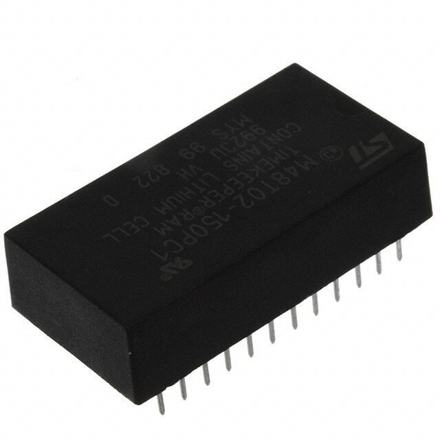
PCF8523 NXP Semiconductors Real-Time Clock (RTC) and calendar 4. Ordering information Table 1. Ordering information Type number Package Name Description Version PCF8523T SO8 plastic small outline package; 8 leads; SOT96-1 body width 3.9mm PCF8523TK HVSON8 plastic thermal enhanced very thin small outline SOT909-1 package; no leads; 8 terminals; body 4 4 0.85mm PCF8523TS TSSOP14 plastic thin shrink small outline package; 14 leads; SOT402-1 bodywidth 4.4mm PCF8523U bare die 12 bumps (6-6) PCF8523U 4.1 Ordering options Table 2. Ordering opt ions Product type Sales item (12NC) Orderable part IC Delivery form number number revision PCF8523T/1 935293581118 PCF8523T/1,118 1 tape and reel, 13 inch PCF8523TK/1 935293573118 PCF8523TK/1,118 1 tape and reel, 13 inch PCF8523TS/1 935291196112 PCF8523TS/1,112 1 tube 935291196118 PCF8523TS/1,118 1 tape and reel, 13 inch PCF8523U/12AA/1 935293887005 PCF8523U/12AA/1,00 1 chips with bumps[1], sawn wafer on Film Frame Carrier (FFC) [1] Bump hardness see Table53. Table 3. PCF8523U w afer information Type number Wafer thickness Wafer diameter FFC for wafer size Marking of bad die PCF8523U/12AA/1 200 m 6 inch 8 inch wafer mapping 5. Marking Table 4. Marking codes Type number Marking code PCF8523T/1 8523T PCF8523TK/1 8523 PCF8523TS/1 8523TS PCF8523U/12AA/1 PC8523-1 PCF8523 All information provided in this document is subject to legal disclaimers. © NXP Semiconductors N.V. 2015. All rights reserved. Product data sheet Rev. 7 — 28 April 2015 2 of 78
PCF8523 NXP Semiconductors Real-Time Clock (RTC) and calendar 6. Block diagram (cid:50)(cid:54)(cid:38)(cid:44) (cid:38)(cid:47)(cid:46)(cid:50)(cid:56)(cid:55) (cid:38)(cid:50)(cid:54)(cid:38)(cid:44) (cid:50)(cid:54)(cid:38)(cid:44)(cid:47)(cid:47)(cid:36)(cid:55)(cid:50)(cid:53)(cid:3) (cid:39)(cid:44)(cid:57)(cid:44)(cid:39)(cid:40)(cid:53) (cid:38)(cid:47)(cid:50)(cid:38)(cid:46)(cid:3)(cid:50)(cid:56)(cid:55) (cid:22)(cid:21)(cid:17)(cid:26)(cid:25)(cid:27)(cid:3)(cid:78)(cid:43)(cid:93) (cid:50)(cid:54)(cid:38)(cid:50) (cid:38)(cid:50)(cid:54)(cid:38)(cid:50) (cid:9) (cid:44)(cid:49)(cid:55)(cid:20)(cid:18)(cid:38)(cid:47)(cid:46)(cid:50)(cid:56)(cid:55) (cid:57)(cid:39)(cid:39) (cid:37)(cid:36)(cid:55)(cid:55)(cid:40)(cid:53)(cid:60)(cid:3) (cid:38)(cid:47)(cid:50)(cid:38)(cid:46)(cid:3) (cid:44)(cid:49)(cid:55)(cid:40)(cid:53)(cid:53)(cid:56)(cid:51)(cid:55) (cid:37)(cid:36)(cid:38)(cid:46)(cid:56)(cid:51)(cid:3) (cid:38)(cid:36)(cid:47)(cid:44)(cid:37)(cid:53)(cid:36)(cid:55)(cid:44)(cid:50)(cid:49)(cid:3) (cid:57)(cid:37)(cid:36)(cid:55) (cid:54)(cid:58)(cid:44)(cid:55)(cid:38)(cid:43)(cid:16)(cid:50)(cid:57)(cid:40)(cid:53)(cid:3) (cid:50)(cid:41)(cid:41)(cid:54)(cid:40)(cid:55) (cid:38)(cid:44)(cid:53)(cid:38)(cid:56)(cid:55)(cid:53)(cid:60) (cid:57)(cid:54)(cid:54) (cid:54)(cid:60)(cid:54)(cid:55)(cid:40)(cid:48)(cid:3) (cid:51)(cid:50)(cid:58)(cid:40)(cid:53)(cid:16)(cid:50)(cid:49)(cid:3) (cid:38)(cid:50)(cid:49)(cid:55)(cid:53)(cid:50)(cid:47) (cid:53)(cid:40)(cid:54)(cid:40)(cid:55) (cid:53)(cid:40)(cid:36)(cid:47)(cid:16)(cid:55)(cid:44)(cid:48)(cid:40)(cid:3) (cid:38)(cid:47)(cid:50)(cid:38)(cid:46) (cid:54)(cid:39)(cid:36) (cid:44)(cid:21)(cid:38)(cid:16)(cid:37)(cid:56)(cid:54)(cid:3) (cid:44)(cid:49)(cid:55)(cid:40)(cid:53)(cid:41)(cid:36)(cid:38)(cid:40) (cid:54)(cid:38)(cid:47) (cid:36)(cid:47)(cid:36)(cid:53)(cid:48) (cid:44)(cid:49)(cid:55)(cid:21) (cid:55)(cid:44)(cid:48)(cid:40)(cid:53) (cid:51)(cid:38)(cid:41)(cid:27)(cid:24)(cid:21)(cid:22) (cid:19)(cid:20)(cid:22)(cid:68)(cid:68)(cid:68)(cid:22)(cid:19)(cid:24) Fig 1. Block diagram of PCF8523 PCF8523 All information provided in this document is subject to legal disclaimers. © NXP Semiconductors N.V. 2015. All rights reserved. Product data sheet Rev. 7 — 28 April 2015 3 of 78
PCF8523 NXP Semiconductors Real-Time Clock (RTC) and calendar 7. Pinning information 7.1 Pinning (cid:50)(cid:54)(cid:38)(cid:44) (cid:20) (cid:27) (cid:57)(cid:39)(cid:39) (cid:50)(cid:54)(cid:38)(cid:50) (cid:21) (cid:26) (cid:44)(cid:49)(cid:55)(cid:20)(cid:18)(cid:38)(cid:47)(cid:46)(cid:50)(cid:56)(cid:55) (cid:51)(cid:38)(cid:41)(cid:27)(cid:24)(cid:21)(cid:22)(cid:55) (cid:57)(cid:37)(cid:36)(cid:55) (cid:22) (cid:25) (cid:54)(cid:38)(cid:47) (cid:57)(cid:54)(cid:54) (cid:23) (cid:24) (cid:54)(cid:39)(cid:36) (cid:19)(cid:20)(cid:22)(cid:68)(cid:68)(cid:68)(cid:22)(cid:19)(cid:25) Top view. For mechanical details, see Figure39 on page56. Fig 2. Pin configuration for SO8 (PCF8523T) (cid:87)(cid:72)(cid:85)(cid:80)(cid:76)(cid:81)(cid:68)(cid:79)(cid:3)(cid:20)(cid:3) (cid:76)(cid:81)(cid:71)(cid:72)(cid:91)(cid:3)(cid:68)(cid:85)(cid:72)(cid:68) (cid:50)(cid:54)(cid:38)(cid:44) (cid:20) (cid:27) (cid:57)(cid:39)(cid:39) (cid:50)(cid:54)(cid:38)(cid:50) (cid:21) (cid:26) (cid:44)(cid:49)(cid:55)(cid:20)(cid:18)(cid:38)(cid:47)(cid:46)(cid:50)(cid:56)(cid:55) (cid:51)(cid:38)(cid:41)(cid:27)(cid:24)(cid:21)(cid:22)(cid:55)(cid:46) (cid:57)(cid:37)(cid:36)(cid:55) (cid:22) (cid:25) (cid:54)(cid:38)(cid:47) (cid:57)(cid:54)(cid:54) (cid:23) (cid:24) (cid:54)(cid:39)(cid:36) (cid:19)(cid:20)(cid:22)(cid:68)(cid:68)(cid:68)(cid:22)(cid:19)(cid:27) (cid:55)(cid:85)(cid:68)(cid:81)(cid:86)(cid:83)(cid:68)(cid:85)(cid:72)(cid:81)(cid:87)(cid:3)(cid:87)(cid:82)(cid:83)(cid:3)(cid:89)(cid:76)(cid:72)(cid:90) For mechanical details, see Figure40 on page57. Fig 3. Pin configuration for HVSON8 (PCF8523TK) (cid:50)(cid:54)(cid:38)(cid:44) (cid:20) (cid:20)(cid:23) (cid:57)(cid:39)(cid:39) (cid:50)(cid:54)(cid:38)(cid:50) (cid:21) (cid:20)(cid:22) (cid:44)(cid:49)(cid:55)(cid:20)(cid:18)(cid:38)(cid:47)(cid:46)(cid:50)(cid:56)(cid:55) (cid:81)(cid:17)(cid:70)(cid:17) (cid:22) (cid:20)(cid:21) (cid:81)(cid:17)(cid:70)(cid:17) (cid:57)(cid:37)(cid:36)(cid:55) (cid:23) (cid:51)(cid:38)(cid:41)(cid:27)(cid:24)(cid:21)(cid:22)(cid:55)(cid:54) (cid:20)(cid:20) (cid:54)(cid:38)(cid:47) (cid:57)(cid:54)(cid:54) (cid:24) (cid:20)(cid:19) (cid:54)(cid:39)(cid:36) (cid:81)(cid:17)(cid:70)(cid:17) (cid:25) (cid:28) (cid:81)(cid:17)(cid:70)(cid:17) (cid:44)(cid:49)(cid:55)(cid:21) (cid:26) (cid:27) (cid:38)(cid:47)(cid:46)(cid:50)(cid:56)(cid:55) (cid:19)(cid:20)(cid:22)(cid:68)(cid:68)(cid:68)(cid:22)(cid:19)(cid:26) Top view. For mechanical details, see Figure41 on page58. Fig 4. Pin configuration for TSSOP14 (PCF8523TS) PCF8523 All information provided in this document is subject to legal disclaimers. © NXP Semiconductors N.V. 2015. All rights reserved. Product data sheet Rev. 7 — 28 April 2015 4 of 78
PCF8523 NXP Semiconductors Real-Time Clock (RTC) and calendar (cid:50)(cid:54)(cid:38)(cid:44) (cid:21) (cid:20) (cid:57)(cid:39)(cid:39) (cid:20)(cid:21) (cid:44)(cid:49)(cid:55)(cid:20)(cid:18)(cid:38)(cid:47)(cid:46)(cid:50)(cid:56)(cid:55) (cid:50)(cid:54)(cid:38)(cid:50) (cid:22) (cid:20)(cid:20) (cid:81)(cid:17)(cid:70)(cid:17) (cid:51)(cid:38)(cid:41)(cid:27)(cid:24)(cid:21)(cid:22)(cid:56) (cid:20)(cid:19) (cid:54)(cid:38)(cid:47) (cid:57)(cid:37)(cid:36)(cid:55) (cid:23) (cid:57)(cid:54)(cid:54) (cid:24) (cid:28) (cid:54)(cid:39)(cid:36) (cid:81)(cid:17)(cid:70)(cid:17) (cid:25) (cid:44)(cid:49)(cid:55)(cid:21) (cid:26) (cid:27) (cid:38)(cid:47)(cid:46)(cid:50)(cid:56)(cid:55) (cid:19)(cid:20)(cid:22)(cid:68)(cid:68)(cid:68)(cid:22)(cid:20)(cid:26) Viewed from active side. For mechanical details, see Figure42 on page59. Fig 5. Pin configuration for PCF8523U 7.2 Pin description Table 5. Pin descripti on Input or input/output pins must always be at a defined level (V or V ) unless otherwise specified. SS DD Symbol Pin Type Description SO8 HVSON8 TSSOP14 PCF8523U (PCF8523T) (PCF8523TK) (PCF8523TS) OSCI 1 1 1 2 input oscillator input; high-impedance node[1] OSCO 2 2 2 3 output oscillator output; high-impedance node[1] n.c. - - 3, 6, 9, 12[2] 6 and 11[2] - not connected; do not connect and do not use it as feed through V 3 3 4 4 supply battery supply voltage BAT V 4 4[3] 5 5[4] supply ground supply voltage SS INT2 - - 7 7 output interrupt 2 (open-drain, active LOW) CLKOUT[5] - - 8 8 output clock output (open-drain) SDA 5 5 10 9 input/output serial data input/output SCL 6 6 11 10 input serial clock input INT1/CLKOUT[5] 7 7 13 12 output interrupt 1/clock output (open-drain) V 8 8 14 1 supply supply voltage DD [1] Wire length between quartz and package should be minimized. [2] For manufacturing tests only; do not connect it and do not use it. [3] The die paddle (exposed pad) is connected to V and should be electrically isolated. SS [4] The substrate (rear side of the die) is connected to V and should be electrically isolated. SS [5] The PCF8523 can either drive the CLKOUT or the INT1. PCF8523 All information provided in this document is subject to legal disclaimers. © NXP Semiconductors N.V. 2015. All rights reserved. Product data sheet Rev. 7 — 28 April 2015 5 of 78
PCF8523 NXP Semiconductors Real-Time Clock (RTC) and calendar 8. Functional description The PCF8523 contains: • 20 8-bit registers with an auto-incrementing address register • An on-chip 32.768kHz oscillator with two integrated load capacitors • A frequency divider, which provides the source clock for the Real-Time Clock (RTC) • A programmable clock output • A 1Mbit/s I2C-bus interface • An offset register, which allows fine-tuning of the clock All 20registers are designed as addressable 8-bit registers although not all bits are implemented. • The first three registers (memory address00h, 01h,and02h) are used as control and status registers • The addresses03h through09h are used as counters for the clock function (seconds up to years) • Addresses 0Ah through 0Dh define the alarm condition • Address 0Eh defines the offset calibration • Address 0Fh defines the clock-out mode and the addresses 10h and 12h the timer mode • Addresses 11h and 13h are used for the timers The registers Seconds, Minutes, Hours, Days, Weekdays, Months, and Years are all coded in Binary Coded Decimal (BCD) format. Other registers are either bit-wise or standard binary. When one of the RTC registers is read, the contents of all counters are frozen. Therefore, faulty reading of the clock and calendar during a carry condition is prevented. The PCF8523 has a battery backup input pin and battery switch-over circuit. The battery switch-over circuit monitors the main power supply and switches automatically to the backup battery when a power failure condition is detected. Accurate timekeeping is maintained even when the main power supply is interrupted. A battery low detection circuit monitors the status of the battery. When the battery voltage goes below a certain threshold value, a flag is set to indicate that the battery must be replaced soon. This ensures the integrity of the data during periods of battery backup. PCF8523 All information provided in this document is subject to legal disclaimers. © NXP Semiconductors N.V. 2015. All rights reserved. Product data sheet Rev. 7 — 28 April 2015 6 of 78
PCF8523 NXP Semiconductors Real-Time Clock (RTC) and calendar 8.1 Registers overview The 20 registers of the PCF8523 are auto-incrementing after each read or write data byte up to register 13h. After register 13h, the auto-incrementing will wrap around to address 00h (see Figure6). (cid:68)(cid:71)(cid:71)(cid:85)(cid:72)(cid:86)(cid:86)(cid:3)(cid:85)(cid:72)(cid:74)(cid:76)(cid:86)(cid:87)(cid:72)(cid:85) (cid:19)(cid:19)(cid:75) (cid:19)(cid:20)(cid:75) (cid:19)(cid:21)(cid:75) (cid:68)(cid:88)(cid:87)(cid:82)(cid:16)(cid:76)(cid:81)(cid:70)(cid:85)(cid:72)(cid:80)(cid:72)(cid:81)(cid:87) (cid:19)(cid:22)(cid:75) (cid:17)(cid:17)(cid:17) (cid:20)(cid:20)(cid:75) (cid:20)(cid:21)(cid:75) (cid:90)(cid:85)(cid:68)(cid:83)(cid:3)(cid:68)(cid:85)(cid:82)(cid:88)(cid:81)(cid:71) (cid:20)(cid:22)(cid:75) (cid:19)(cid:20)(cid:22)(cid:68)(cid:68)(cid:68)(cid:22)(cid:19)(cid:28) Fig 6. Auto-incrementing of the registers Table 6. Registers ov erview Bit positions labeled as- are not implemented and will return a 0 when read. Bit T must always be written with logic0. Address Register name Bit 7 6 5 4 3 2 1 0 Control registers 00h Control_1 CAP_SEL T STOP SR 12_24 SIE AIE CIE 01h Control_2 WTAF CTAF CTBF SF AF WTAIE CTAIE CTBIE 02h Control_3 PM[2:0] - BSF BLF BSIE BLIE Time and date registers 03h Seconds OS SECONDS (0 to 59) 04h Minutes - MINUTES (0 to 59) 05h Hours - - AMPM HOURS (1 to 12 in 12hour mode) HOURS (0 to 23 in 24hour mode) 06h Days - - DAYS (1 to 31) 07h Weekdays - - - - - WEEKDAYS (0 to 6) 08h Months - - - MONTHS (1 to 12) 09h Years YEARS (0 to 99) Alarm registers 0Ah Minute_alarm AEN_M MINUTE_ALARM (0 to 59) 0Bh Hour_alarm AEN_H - AMPM HOUR_ALARM (1 to 12 in 12hour mode) - HOUR_ALARM (0 to 23 in 24hour mode) 0Ch Day_alarm AEN_D - DAY_ALARM (1 to 31) 0Dh Weekday_alarm AEN_W - - - - WEEKDAY_ALARM (0 to 6) Offset register 0Eh Offset MODE OFFSET[6:0] PCF8523 All information provided in this document is subject to legal disclaimers. © NXP Semiconductors N.V. 2015. All rights reserved. Product data sheet Rev. 7 — 28 April 2015 7 of 78
PCF8523 NXP Semiconductors Real-Time Clock (RTC) and calendar Table 6. Registers overview …continued Bit positions labeled as- are not implemented and will return a 0 when read. Bit T must always be written with logic0. Address Register name Bit 7 6 5 4 3 2 1 0 CLOCKOUT and timer registers 0Fh Tmr_CLKOUT_ctrl TAM TBM COF[2:0] TAC[1:0] TBC 10h Tmr_A_freq_ctrl - - - - - TAQ[2:0] 11h Tmr_A_reg T_A[7:0] 12h Tmr_B_freq_ctrl - TBW[2:0] - TBQ[2:0] 13h Tmr_B_reg T_B[7:0] PCF8523 All information provided in this document is subject to legal disclaimers. © NXP Semiconductors N.V. 2015. All rights reserved. Product data sheet Rev. 7 — 28 April 2015 8 of 78
PCF8523 NXP Semiconductors Real-Time Clock (RTC) and calendar 8.2 Control and status registers 8.2.1 Register Control_1 Table 7. Control_1 - control and status register 1 (address00h) bit description Bit Symbol Value Description 7 CAP_SEL internal oscillator capacitor selection for quartz crystals with a corresponding load capacitance 0[1] 7pF 1 12.5pF 6 T 0[1][2] unused 5 STOP 0[1] RTC time circuits running 1 RTC time circuits frozen; RTC divider chain flip-flops are asynchronously set logic0; CLKOUT at 32.768kHz, 16.384 kHz, or 8.192kHz is still available 4 SR 0[1][3] no software reset 1 initiate software reset 3 12_24 0[1] 24 hour mode is selected 1 12 hour mode is selected 2 SIE 0[1] second interrupt disabled 1 second interrupt enabled 1 AIE 0[1] alarm interrupt disabled 1 alarm interrupt enabled 0 CIE 0[1] no correction interrupt generated 1 interrupt pulses are generated at every correction cycle (see Section8.8) [1] Default value. [2] Must always be written with logic 0. [3] For a software reset, 01011000 (58h) must be sent to register Control_1 (see Section8.3). Bit SR always returns 0 when read. PCF8523 All information provided in this document is subject to legal disclaimers. © NXP Semiconductors N.V. 2015. All rights reserved. Product data sheet Rev. 7 — 28 April 2015 9 of 78
PCF8523 NXP Semiconductors Real-Time Clock (RTC) and calendar 8.2.2 Register Control_2 Table 8. Control_2 - control and status register 2 (address01h) bit description Bit Symbol Value Description 7 WTAF 0[1] no watchdog timer A interrupt generated 1 flag set when watchdog timer A interrupt generated; flag is read-only and cleared by reading register Control_2 6 CTAF 0[1] no countdown timer A interrupt generated 1 flag set when countdown timer A interrupt generated; flag must be cleared to clear interrupt 5 CTBF 0[1] no countdown timer B interrupt generated 1 flag set when countdown timer B interrupt generated; flag must be cleared to clear interrupt 4 SF 0[1] no second interrupt generated 1 flag set when second interrupt generated; flag must be cleared to clear interrupt 3 AF 0[1] no alarm interrupt generated 1 flag set when alarm triggered; flag must be cleared to clear interrupt 2 WTAIE 0[1] watchdog timer A interrupt is disabled 1 watchdog timer A interrupt is enabled 1 CTAIE 0[1] countdown timer A interrupt is disabled 1 countdown timer A interrupt is enabled 0 CTBIE 0[1] countdown timer B interrupt is disabled 1 countdown timer B interrupt is enabled [1] Default value. PCF8523 All information provided in this document is subject to legal disclaimers. © NXP Semiconductors N.V. 2015. All rights reserved. Product data sheet Rev. 7 — 28 April 2015 10 of 78
PCF8523 NXP Semiconductors Real-Time Clock (RTC) and calendar 8.2.3 Register Control_3 Table 9. Control_3 - control and status register 3 (address02h) bit description Bit Symbol Value Description 7 to 5 PM[2:0] see Table11[1] battery switch-over and battery low detection control 4 - - unused 3 BSF 0[2] no battery switch-over interrupt generated 1 flag set when battery switch-over occurs; flag must be cleared to clear interrupt 2 BLF 0[2] battery status ok 1 battery status low; flag is read-only 1 BSIE 0[2] no interrupt generated from battery switch-over flag,BSF 1 interrupt generated when BSF is set 0 BLIE 0[2] no interrupt generated from battery low flag,BLF 1 interrupt generated when BLF is set [1] Default value is 111. [2] Default value. PCF8523 All information provided in this document is subject to legal disclaimers. © NXP Semiconductors N.V. 2015. All rights reserved. Product data sheet Rev. 7 — 28 April 2015 11 of 78
PCF8523 NXP Semiconductors Real-Time Clock (RTC) and calendar 8.3 Reset A reset is automatically generated at power-on. A reset can also be initiated with the software reset command. Software reset command means setting bits 6, 4, and 3 in register Control_1 (00h) logic 1 and all other bits logic 0 by sending the bit sequence 01011000 (58h), see Figure7. (cid:86)(cid:79)(cid:68)(cid:89)(cid:72)(cid:3)(cid:68)(cid:71)(cid:71)(cid:85)(cid:72)(cid:86)(cid:86)(cid:3)(cid:69)(cid:92)(cid:87)(cid:72) (cid:53)(cid:18)(cid:58) (cid:68)(cid:71)(cid:71)(cid:85)(cid:72)(cid:86)(cid:86)(cid:3)(cid:19)(cid:19)(cid:75) (cid:86)(cid:82)(cid:73)(cid:87)(cid:90)(cid:68)(cid:85)(cid:72)(cid:3)(cid:85)(cid:72)(cid:86)(cid:72)(cid:87)(cid:3)(cid:24)(cid:27)(cid:75) (cid:54)(cid:39)(cid:36) (cid:86) (cid:20) (cid:20) (cid:19) (cid:20) (cid:19) (cid:19) (cid:19) (cid:19) (cid:36) (cid:19) (cid:19) (cid:19) (cid:19) (cid:19) (cid:19) (cid:19) (cid:19) (cid:36) (cid:19) (cid:20) (cid:19) (cid:20) (cid:20) (cid:19) (cid:19) (cid:19) (cid:36) (cid:51)(cid:18)(cid:54) (cid:54)(cid:38)(cid:47) (cid:76)(cid:81)(cid:87)(cid:72)(cid:85)(cid:81)(cid:68)(cid:79) (cid:85)(cid:72)(cid:86)(cid:72)(cid:87)(cid:3)(cid:86)(cid:76)(cid:74)(cid:81)(cid:68)(cid:79) (cid:19)(cid:20)(cid:22)(cid:68)(cid:68)(cid:68)(cid:22)(cid:21)(cid:19) Fig 7. Software reset command Table 10. Register reset values Bits labeled X are undefined at power-on and unchanged by subsequent resets. Bits labeled - are not implemented. Address Register name Bit 7 6 5 4 3 2 1 0 00h Control_1 0 0 0 0 0 0 0 0 01h Control_2 0 0 0 0 0 0 0 0 02h Control_3 1 1 1 - 0 0 0 0 03h Seconds 1 X X X X X X X 04h Minutes - X X X X X X X 05h Hours - - X X X X X X 06h Days - - X X X X X X 07h Weekdays - - - - - X X X 08h Months - - - X X X X X 09h Years X X X X X X X X 0Ah Minute_alarm 1 X X X X X X X 0Bh Hour_alarm 1 - X X X X X X 0Ch Day_alarm 1 - X X X X X X 0Dh Weekday_alarm 1 - - - - X X X 0Eh Offset 0 0 0 0 0 0 0 0 0Fh Tmr_CLKOUT_ctrl 0 0 0 0 0 0 0 0 10h Tmr_A_freq_ctrl - - - - - 1 1 1 11h Tmr_A_reg X X X X X X X X 12h Tmr_B_freq_ctrl - 0 0 0 - 1 1 1 13h Tmr_B_reg X X X X X X X X PCF8523 All information provided in this document is subject to legal disclaimers. © NXP Semiconductors N.V. 2015. All rights reserved. Product data sheet Rev. 7 — 28 April 2015 12 of 78
PCF8523 NXP Semiconductors Real-Time Clock (RTC) and calendar After reset, the following mode is entered: • 32.768 kHz CLKOUT active • 24 hour mode is selected • Register Offset is set logic 0 • No alarms set • Timers disabled • No interrupts enabled • Battery switch-over is disabled • Battery low detection is disabled • 7pF of internal oscillator capacitor selected 8.4 Interrupt function Active low interrupt signals are available at pin INT1/CLKOUT and INT2. Pin INT1/CLKOUT has both functions of INT1 and CLKOUT combined, that is that either the CLKOUT or the INT1 can be used. Therefore the usage of INT1 requires that CLKOUT is disabled. INT1 Interrupt output may be sourced from different places: • Second timer • Timer A • Timer B • Alarm • Battery switch-over • Battery low detection • Clock offset correction pulse INT2 interrupt output is sourced only from timer B: The control bit TAM (register Tmr_CLKOUT_ctrl) is used to configure whether the interrupts generated from the second interrupt timer and timer A are pulsed signals or a permanently active signal. The control bit TBM (register Tmr_CLKOUT_ctrl) is used to configure whether the interrupt generated from timer B is a pulsed signal or a permanently active signal. All the other interrupt sources generate a permanently active interrupt signal, which follows the status of the corresponding flags. • The flags SF, CTAF, CTBF, AF, and BSF can be cleared by using the interface • WTAF is read only. Reading of the register Control_2 (01h) automatically resets WTAF (WTAF=0) and clears the interrupt • The flag BLF is read only. It is cleared automatically from the battery low detection circuit when the battery is replaced PCF8523 All information provided in this document is subject to legal disclaimers. © NXP Semiconductors N.V. 2015. All rights reserved. Product data sheet Rev. 7 — 28 April 2015 13 of 78
PCF8523 NXP Semiconductors Real-Time Clock (RTC) and calendar (cid:87)(cid:82)(cid:3)(cid:76)(cid:81)(cid:87)(cid:72)(cid:85)(cid:73)(cid:68)(cid:70)(cid:72)(cid:29) (cid:36)(cid:44)(cid:40) (cid:36)(cid:41)(cid:29)(cid:3)(cid:36)(cid:47)(cid:36)(cid:53)(cid:48) (cid:85)(cid:72)(cid:68)(cid:71)(cid:3)(cid:36)(cid:41) (cid:86)(cid:72)(cid:87)(cid:3)(cid:68)(cid:79)(cid:68)(cid:85)(cid:80) (cid:41)(cid:47)(cid:36)(cid:42) (cid:73)(cid:79)(cid:68)(cid:74)(cid:15)(cid:3)(cid:36)(cid:41) (cid:54)(cid:40)(cid:55) (cid:38)(cid:47)(cid:40)(cid:36)(cid:53) (cid:73)(cid:85)(cid:82)(cid:80)(cid:3)(cid:76)(cid:81)(cid:87)(cid:72)(cid:85)(cid:73)(cid:68)(cid:70)(cid:72)(cid:29) (cid:70)(cid:79)(cid:72)(cid:68)(cid:85)(cid:3)(cid:36)(cid:41) (cid:38)(cid:44)(cid:40) (cid:51)(cid:56)(cid:47)(cid:54)(cid:40) (cid:82)(cid:73)(cid:73)(cid:86)(cid:72)(cid:87)(cid:3)(cid:70)(cid:76)(cid:85)(cid:70)(cid:88)(cid:76)(cid:87)(cid:29) (cid:42)(cid:40)(cid:49)(cid:40)(cid:53)(cid:36)(cid:55)(cid:50)(cid:53)(cid:3)(cid:24) (cid:68)(cid:71)(cid:71)(cid:18)(cid:86)(cid:88)(cid:69)(cid:87)(cid:85)(cid:68)(cid:70)(cid:87)(cid:3)(cid:83)(cid:88)(cid:79)(cid:86)(cid:72) (cid:54)(cid:40)(cid:55) (cid:38)(cid:47)(cid:40)(cid:36)(cid:53) (cid:73)(cid:85)(cid:82)(cid:80)(cid:3)(cid:76)(cid:81)(cid:87)(cid:72)(cid:85)(cid:73)(cid:68)(cid:70)(cid:72)(cid:29) (cid:70)(cid:79)(cid:72)(cid:68)(cid:85)(cid:3)(cid:38)(cid:44)(cid:40) (cid:87)(cid:82)(cid:3)(cid:76)(cid:81)(cid:87)(cid:72)(cid:85)(cid:73)(cid:68)(cid:70)(cid:72)(cid:29) (cid:37)(cid:54)(cid:44)(cid:40) (cid:37)(cid:54)(cid:41)(cid:29)(cid:3)(cid:37)(cid:36)(cid:55)(cid:55)(cid:40)(cid:53)(cid:60) (cid:85)(cid:72)(cid:68)(cid:71)(cid:3)(cid:37)(cid:54)(cid:41) (cid:86)(cid:72)(cid:87)(cid:3)(cid:69)(cid:68)(cid:87)(cid:87)(cid:72)(cid:85)(cid:92) (cid:41)(cid:47)(cid:36)(cid:42) (cid:73)(cid:79)(cid:68)(cid:74)(cid:15)(cid:3)(cid:37)(cid:54)(cid:41) (cid:54)(cid:40)(cid:55) (cid:38)(cid:47)(cid:40)(cid:36)(cid:53) (cid:73)(cid:85)(cid:82)(cid:80)(cid:3)(cid:76)(cid:81)(cid:87)(cid:72)(cid:85)(cid:73)(cid:68)(cid:70)(cid:72)(cid:29) (cid:70)(cid:79)(cid:72)(cid:68)(cid:85)(cid:3)(cid:37)(cid:54)(cid:41) (cid:87)(cid:82)(cid:3)(cid:76)(cid:81)(cid:87)(cid:72)(cid:85)(cid:73)(cid:68)(cid:70)(cid:72)(cid:29) (cid:37)(cid:47)(cid:44)(cid:40) (cid:37)(cid:47)(cid:41)(cid:29)(cid:3)(cid:37)(cid:36)(cid:55)(cid:55)(cid:40)(cid:53)(cid:60) (cid:85)(cid:72)(cid:68)(cid:71)(cid:3)(cid:37)(cid:47)(cid:41) (cid:86)(cid:72)(cid:87)(cid:3)(cid:69)(cid:68)(cid:87)(cid:87)(cid:72)(cid:85)(cid:92) (cid:47)(cid:50)(cid:58)(cid:3)(cid:41)(cid:47)(cid:36)(cid:42) (cid:79)(cid:82)(cid:90)(cid:3)(cid:73)(cid:79)(cid:68)(cid:74)(cid:15)(cid:3)(cid:37)(cid:47)(cid:41) (cid:54)(cid:40)(cid:55) (cid:38)(cid:47)(cid:40)(cid:36)(cid:53) (cid:73)(cid:85)(cid:82)(cid:80)(cid:3)(cid:69)(cid:68)(cid:87)(cid:87)(cid:72)(cid:85)(cid:92) (cid:44)(cid:49)(cid:55)(cid:20) (cid:79)(cid:82)(cid:90)(cid:3)(cid:71)(cid:72)(cid:87)(cid:72)(cid:70)(cid:87)(cid:76)(cid:82)(cid:81) (cid:70)(cid:76)(cid:85)(cid:70)(cid:88)(cid:76)(cid:87)(cid:29)(cid:3)(cid:70)(cid:79)(cid:72)(cid:68)(cid:85)(cid:3)(cid:37)(cid:47)(cid:41) (cid:44)(cid:49)(cid:55)(cid:20)(cid:18)(cid:38)(cid:47)(cid:46)(cid:50)(cid:56)(cid:55) (cid:87)(cid:82)(cid:3)(cid:76)(cid:81)(cid:87)(cid:72)(cid:85)(cid:73)(cid:68)(cid:70)(cid:72)(cid:29) (cid:54)(cid:44)(cid:40) (cid:54)(cid:40)(cid:38)(cid:50)(cid:54)(cid:49)(cid:41)(cid:39)(cid:29)(cid:3)(cid:41)(cid:47)(cid:36)(cid:42) (cid:85)(cid:72)(cid:68)(cid:71)(cid:3)(cid:54)(cid:41) (cid:19) (cid:54)(cid:44)(cid:40) (cid:38)(cid:47)(cid:46)(cid:50)(cid:56)(cid:55) (cid:54)(cid:40)(cid:38)(cid:50)(cid:49)(cid:39)(cid:54)(cid:3)(cid:38)(cid:50)(cid:56)(cid:49)(cid:55)(cid:40)(cid:53) (cid:54)(cid:40)(cid:55) (cid:38)(cid:47)(cid:40)(cid:36)(cid:53) (cid:51)(cid:56)(cid:47)(cid:54)(cid:40) (cid:20) (cid:42)(cid:40)(cid:49)(cid:40)(cid:53)(cid:36)(cid:55)(cid:50)(cid:53)(cid:3)(cid:20) (cid:55)(cid:53)(cid:44)(cid:42)(cid:42)(cid:40)(cid:53) (cid:38)(cid:47)(cid:40)(cid:36)(cid:53) (cid:55)(cid:36)(cid:48) (cid:73)(cid:85)(cid:82)(cid:80)(cid:3)(cid:76)(cid:81)(cid:87)(cid:72)(cid:85)(cid:73)(cid:68)(cid:70)(cid:72)(cid:29) (cid:70)(cid:79)(cid:72)(cid:68)(cid:85)(cid:3)(cid:54)(cid:41) (cid:38)(cid:55)(cid:36)(cid:41)(cid:29) (cid:87)(cid:82)(cid:3)(cid:76)(cid:81)(cid:87)(cid:72)(cid:85)(cid:73)(cid:68)(cid:70)(cid:72)(cid:29) (cid:55)(cid:36)(cid:48) (cid:38)(cid:50)(cid:56)(cid:49)(cid:55)(cid:39)(cid:50)(cid:58)(cid:49) (cid:85)(cid:72)(cid:68)(cid:71)(cid:3)(cid:38)(cid:55)(cid:36)(cid:41) (cid:38)(cid:55)(cid:36)(cid:44)(cid:40) (cid:19) (cid:38)(cid:50)(cid:56)(cid:49)(cid:55)(cid:39)(cid:50)(cid:58)(cid:49) (cid:55)(cid:44)(cid:48)(cid:40)(cid:53)(cid:3)(cid:36)(cid:3)(cid:41)(cid:47)(cid:36)(cid:42) (cid:38)(cid:50)(cid:56)(cid:49)(cid:55)(cid:40)(cid:53)(cid:3)(cid:36) (cid:54)(cid:40)(cid:55) (cid:38)(cid:47)(cid:40)(cid:36)(cid:53) (cid:20) (cid:55)(cid:36)(cid:38)(cid:3)(cid:32)(cid:3)(cid:19)(cid:20) (cid:51)(cid:56)(cid:47)(cid:54)(cid:40) (cid:40)(cid:49)(cid:36)(cid:37)(cid:47)(cid:40) (cid:42)(cid:40)(cid:49)(cid:40)(cid:53)(cid:36)(cid:55)(cid:50)(cid:53)(cid:3)(cid:21) (cid:55)(cid:53)(cid:44)(cid:42)(cid:42)(cid:40)(cid:53) (cid:38)(cid:47)(cid:40)(cid:36)(cid:53) (cid:73)(cid:85)(cid:82)(cid:80)(cid:3)(cid:76)(cid:81)(cid:87)(cid:72)(cid:85)(cid:73)(cid:68)(cid:70)(cid:72)(cid:29) (cid:70)(cid:79)(cid:72)(cid:68)(cid:85)(cid:3)(cid:38)(cid:55)(cid:36)(cid:41) (cid:58)(cid:55)(cid:36)(cid:41)(cid:29) (cid:87)(cid:82)(cid:3)(cid:76)(cid:81)(cid:87)(cid:72)(cid:85)(cid:73)(cid:68)(cid:70)(cid:72)(cid:29) (cid:55)(cid:36)(cid:48) (cid:58)(cid:36)(cid:55)(cid:38)(cid:43)(cid:3)(cid:39)(cid:50)(cid:42) (cid:85)(cid:72)(cid:68)(cid:71)(cid:3)(cid:58)(cid:55)(cid:36)(cid:41) (cid:19) (cid:58)(cid:55)(cid:36)(cid:44)(cid:40) (cid:58)(cid:36)(cid:55)(cid:38)(cid:43)(cid:39)(cid:50)(cid:42) (cid:55)(cid:44)(cid:48)(cid:40)(cid:53)(cid:3)(cid:41)(cid:47)(cid:36)(cid:42) (cid:38)(cid:50)(cid:56)(cid:49)(cid:55)(cid:40)(cid:53)(cid:3)(cid:36) (cid:54)(cid:40)(cid:55) (cid:38)(cid:47)(cid:40)(cid:36)(cid:53) (cid:55)(cid:36)(cid:38)(cid:3)(cid:32)(cid:3)(cid:20)(cid:19) (cid:40)(cid:49)(cid:36)(cid:37)(cid:47)(cid:40) (cid:51)(cid:56)(cid:47)(cid:54)(cid:40) (cid:20) (cid:42)(cid:40)(cid:49)(cid:40)(cid:53)(cid:36)(cid:55)(cid:50)(cid:53)(cid:3)(cid:22) (cid:48)(cid:38)(cid:56)(cid:3)(cid:79)(cid:82)(cid:68)(cid:71)(cid:76)(cid:81)(cid:74) (cid:55)(cid:53)(cid:44)(cid:42)(cid:42)(cid:40)(cid:53) (cid:38)(cid:47)(cid:40)(cid:36)(cid:53) (cid:90)(cid:68)(cid:87)(cid:70)(cid:75)(cid:71)(cid:82)(cid:74)(cid:3)(cid:70)(cid:82)(cid:88)(cid:81)(cid:87)(cid:72)(cid:85) (cid:82)(cid:85)(cid:3)(cid:85)(cid:72)(cid:68)(cid:71)(cid:76)(cid:81)(cid:74)(cid:3)(cid:58)(cid:55)(cid:36)(cid:41) (cid:38)(cid:55)(cid:37)(cid:41)(cid:29) (cid:87)(cid:82)(cid:3)(cid:76)(cid:81)(cid:87)(cid:72)(cid:85)(cid:73)(cid:68)(cid:70)(cid:72)(cid:29) (cid:55)(cid:37)(cid:48) (cid:38)(cid:50)(cid:56)(cid:49)(cid:55)(cid:39)(cid:50)(cid:58)(cid:49) (cid:85)(cid:72)(cid:68)(cid:71)(cid:3)(cid:38)(cid:55)(cid:37)(cid:41) (cid:38)(cid:55)(cid:37)(cid:44)(cid:40) (cid:19) (cid:38)(cid:50)(cid:56)(cid:49)(cid:55)(cid:39)(cid:50)(cid:58)(cid:49) (cid:55)(cid:44)(cid:48)(cid:40)(cid:53)(cid:3)(cid:37)(cid:3)(cid:41)(cid:47)(cid:36)(cid:42) (cid:38)(cid:50)(cid:56)(cid:49)(cid:55)(cid:40)(cid:53)(cid:3)(cid:37) (cid:54)(cid:40)(cid:55) (cid:38)(cid:47)(cid:40)(cid:36)(cid:53) (cid:20) (cid:44)(cid:49)(cid:55)(cid:21) (cid:55)(cid:37)(cid:38)(cid:3)(cid:32)(cid:3)(cid:20) (cid:51)(cid:56)(cid:47)(cid:54)(cid:40) (cid:40)(cid:49)(cid:36)(cid:37)(cid:47)(cid:40) (cid:42)(cid:40)(cid:49)(cid:40)(cid:53)(cid:36)(cid:55)(cid:50)(cid:53)(cid:3)(cid:23) (cid:55)(cid:53)(cid:44)(cid:42)(cid:42)(cid:40)(cid:53) (cid:38)(cid:47)(cid:40)(cid:36)(cid:53) (cid:73)(cid:85)(cid:82)(cid:80)(cid:3)(cid:76)(cid:81)(cid:87)(cid:72)(cid:85)(cid:73)(cid:68)(cid:70)(cid:72)(cid:29) (cid:70)(cid:79)(cid:72)(cid:68)(cid:85)(cid:3)(cid:38)(cid:55)(cid:37)(cid:41) (cid:19)(cid:20)(cid:22)(cid:68)(cid:68)(cid:68)(cid:22)(cid:22)(cid:19) When SIE, CTAIE, WTAIE, CTBIE, AIE, CIE, BSIE, BLIE, and clock-out are disabled, then INT1 remains high-impedance. When CTBIE is disabled, then INT2 remains high-impedance. Fig 8. Interrupt block diagram PCF8523 All information provided in this document is subject to legal disclaimers. © NXP Semiconductors N.V. 2015. All rights reserved. Product data sheet Rev. 7 — 28 April 2015 14 of 78
PCF8523 NXP Semiconductors Real-Time Clock (RTC) and calendar 8.5 Power management functions The PCF8523 has two power supply pins: • V - the main power supply input pin DD • V - the battery backup input pin BAT The PCF8523 has two power management functions implemented: • Battery switch-over function • Battery low detection function The power management functions are controlled by the control bits PM[2:0] in register Control_3 (02h): Table 11. Power management function control bits PM[2:0] Function 000 battery switch-over function is enabled in standard mode; battery low detection function is enabled 001 battery switch-over function is enabled in direct switching mode; battery low detection function is enabled 010,011[1] battery switch-over function is disabled - only one power supply (V ); DD battery low detection function is enabled 100 battery switch-over function is enabled in standard mode; battery low detection function is disabled 101 battery switch-over function is enabled in direct switching mode; battery low detection function is disabled 110 not allowed 111[2][3] battery switch-over function is disabled - only one power supply (V ); DD battery low detection function is disabled [1] When the battery switch-over function is disabled, the PCF8523 works only with the power supply V . DD [2] When the battery switch-over function is disabled, the PCF8523 works only with the power supply V and DD the battery low detection function is disabled. VBAT must be put to VDD. [3] Default value. 8.5.1 Standby mode When the device is first powered up from the battery (V ) but without a main supply BAT (V ), the PCF8523 automatically enters the standby mode. In standby mode, the DD PCF8523 does not draw any power from the backup battery until the device is powered up from the main power supply V . Thereafter, the device switches over to battery backup DD mode whenever the main power supply V is lost. DD It is also possible to enter into standby mode when the chip is already supplied by the main power supply V and a backup battery is connected. To enter the standby mode, DD the power management control bits PM[2:0] have to be set logic 111. Then the main power supply V must be removed. As a result of it, the PCF8523 enters the standby DD mode and does not draw any current from the backup battery before it is powered up again from main supply V . DD PCF8523 All information provided in this document is subject to legal disclaimers. © NXP Semiconductors N.V. 2015. All rights reserved. Product data sheet Rev. 7 — 28 April 2015 15 of 78
PCF8523 NXP Semiconductors Real-Time Clock (RTC) and calendar 8.5.2 Battery switch-over function The PCF8523 has a backup battery switch-over circuit. It monitors the main power supply V and switches automatically to the backup battery when a power failure condition is DD detected. One of two operation modes can be selected: • Standard mode: the power failure condition happens when: V < V AND V <V DD BAT DD th(sw)bat • Direct switching mode: the power failure condition happens when V < V . DD BAT Direct switching from V to V without requiring V to drop below V DD BAT DD th(sw)bat V is the battery switch threshold voltage. Typical value is 2.5V. th(sw)bat Generation of interrupts from the battery switch-over is controlled via the BSIE bit (see register Control_2). If BSIE is enabled, the INT1 follows the status of bit BLF (register Control_3). Clearing BLF immediately clears INT1. When a power failure condition occurs and the power supply switches to the battery, the following sequence occurs: 1. The battery switch flag BSF (register Control_3) is set logic 1 2. An interrupt is generated if the control bit BSIE (register Control_3) is enabled The battery switch flag BSF can be cleared by using the interface after the power supply has switched to V . It must be cleared to clear the interrupt. DD The interface is disabled in battery backup operation: • Interface inputs are not recognized, preventing extraneous data being written to the device • Interface outputs are high-impedance PCF8523 All information provided in this document is subject to legal disclaimers. © NXP Semiconductors N.V. 2015. All rights reserved. Product data sheet Rev. 7 — 28 April 2015 16 of 78
PCF8523 NXP Semiconductors Real-Time Clock (RTC) and calendar 8.5.2.1 Standard mode If V > V OR V >V , the internal power supply is V . DD BAT DD th(sw)bat DD If V < V AND V <V , the internal power supply is V . DD BAT DD th(sw)bat BAT (cid:69)(cid:68)(cid:70)(cid:78)(cid:88)(cid:83)(cid:3)(cid:69)(cid:68)(cid:87)(cid:87)(cid:72)(cid:85)(cid:92)(cid:3)(cid:82)(cid:83)(cid:72)(cid:85)(cid:68)(cid:87)(cid:76)(cid:82)(cid:81) (cid:57)(cid:39)(cid:39) (cid:57)(cid:37)(cid:37)(cid:54) (cid:57)(cid:37)(cid:37)(cid:54) (cid:57)(cid:37)(cid:36)(cid:55) (cid:76)(cid:81)(cid:87)(cid:72)(cid:85)(cid:81)(cid:68)(cid:79)(cid:3)(cid:83)(cid:82)(cid:90)(cid:72)(cid:85)(cid:3)(cid:86)(cid:88)(cid:83)(cid:83)(cid:79)(cid:92)(cid:3)(cid:11)(cid:32)(cid:3)(cid:57)(cid:37)(cid:37)(cid:54)(cid:12) (cid:57)(cid:87)(cid:75)(cid:11)(cid:86)(cid:90)(cid:12)(cid:69)(cid:68)(cid:87)(cid:3) (cid:11)(cid:32)(cid:3)(cid:21)(cid:17)(cid:24)(cid:3)(cid:57)(cid:12) (cid:57)(cid:39)(cid:39)(cid:3)(cid:11)(cid:32)(cid:3)(cid:19)(cid:3)(cid:57)(cid:12) (cid:37)(cid:54)(cid:41) (cid:44)(cid:49)(cid:55)(cid:20) (cid:70)(cid:79)(cid:72)(cid:68)(cid:85)(cid:72)(cid:71)(cid:3)(cid:89)(cid:76)(cid:68)(cid:3)(cid:76)(cid:81)(cid:87)(cid:72)(cid:85)(cid:73)(cid:68)(cid:70)(cid:72) (cid:19)(cid:20)(cid:22)(cid:68)(cid:68)(cid:68)(cid:22)(cid:21)(cid:20) Fig 9. Battery switch-over behavior in standard mode and with bit BSIE set logic 1 (enabled) PCF8523 All information provided in this document is subject to legal disclaimers. © NXP Semiconductors N.V. 2015. All rights reserved. Product data sheet Rev. 7 — 28 April 2015 17 of 78
PCF8523 NXP Semiconductors Real-Time Clock (RTC) and calendar 8.5.2.2 Direct switching mode If V > V the internal power supply is V . DD BAT DD If V < V the internal power supply is V . DD BAT BAT The direct switching mode is useful in systems where V is higher than V at all times DD BAT (for example, V = 5V, V = 3.5V). If the V and V values are similar (for DD BAT DD BAT example, V = 3.3V, V 3.0V), the direct switching mode is not recommended. In DD BAT direct switching mode, the power consumption is reduced compared to the standard mode because the monitoring of V and V is not performed. DD th(sw)bat (cid:69)(cid:68)(cid:70)(cid:78)(cid:88)(cid:83)(cid:3)(cid:69)(cid:68)(cid:87)(cid:87)(cid:72)(cid:85)(cid:92)(cid:3)(cid:82)(cid:83)(cid:72)(cid:85)(cid:68)(cid:87)(cid:76)(cid:82)(cid:81) (cid:57)(cid:39)(cid:39) (cid:57)(cid:37)(cid:37)(cid:54) (cid:57)(cid:37)(cid:37)(cid:54) (cid:57)(cid:37)(cid:36)(cid:55) (cid:76)(cid:81)(cid:87)(cid:72)(cid:85)(cid:81)(cid:68)(cid:79)(cid:3)(cid:83)(cid:82)(cid:90)(cid:72)(cid:85)(cid:3)(cid:86)(cid:88)(cid:83)(cid:83)(cid:79)(cid:92)(cid:3)(cid:11)(cid:32)(cid:3)(cid:57)(cid:37)(cid:37)(cid:54)(cid:12) (cid:57)(cid:87)(cid:75)(cid:11)(cid:86)(cid:90)(cid:12)(cid:69)(cid:68)(cid:87)(cid:3) (cid:11)(cid:32)(cid:3)(cid:21)(cid:17)(cid:24)(cid:3)(cid:57)(cid:12) (cid:57)(cid:39)(cid:39)(cid:3)(cid:11)(cid:32)(cid:3)(cid:19)(cid:3)(cid:57)(cid:12) (cid:37)(cid:54)(cid:41) (cid:44)(cid:49)(cid:55)(cid:20)(cid:3) (cid:70)(cid:79)(cid:72)(cid:68)(cid:85)(cid:72)(cid:71)(cid:3)(cid:89)(cid:76)(cid:68)(cid:3)(cid:76)(cid:81)(cid:87)(cid:72)(cid:85)(cid:73)(cid:68)(cid:70)(cid:72) (cid:19)(cid:20)(cid:22)(cid:68)(cid:68)(cid:68)(cid:22)(cid:21)(cid:21) Fig 10. Battery switch-over behavior in direct switching mode and with bit BSIE set logic1 (enabled) 8.5.2.3 Battery switch-over disabled, only one power supply (V ) DD When the battery switch-over function is disabled: • The power supply is applied on the V pin DD • The V pin must be connected to V BAT DD • The battery flag (BSF) is always logic 0 8.5.3 Battery low detection function The PCF8523 has a battery low detection circuit, which monitors the status of the battery V . BAT Generation of interrupts from the battery low detection is controlled via bit BLIE (register Control_3). If BLIE is enabled, the INT1 follows the status of bit BLF (register Control_3). When V drops below the threshold value V (typically 2.5V), the BLF flag BAT th(bat)low (register Control_3) is set to indicate that the battery is low and that it must be replaced. Monitoring of the battery voltage also occurs during battery operation. PCF8523 All information provided in this document is subject to legal disclaimers. © NXP Semiconductors N.V. 2015. All rights reserved. Product data sheet Rev. 7 — 28 April 2015 18 of 78
PCF8523 NXP Semiconductors Real-Time Clock (RTC) and calendar An unreliable battery does not ensure data integrity during periods of backup battery operation. When V drops below the threshold value V , the following sequence occurs (see BAT th(bat)low Figure11): 1. The battery low flag BLF is set logic 1 2. An interrupt is generated if the control bit BLIE (register Control_3) is enabled. The interrupt remains active until the battery is replaced (BLF set logic 0) or when bit BLIE is disabled (BLIE set logic 0) 3. The flag BLF (register Control_3) remains logic1 until the battery is replaced. BLF cannot be cleared using the interface. It is cleared automatically by the battery low detection circuit when the battery is replaced (cid:57)(cid:39)(cid:39)(cid:3)(cid:32)(cid:3)(cid:57)(cid:37)(cid:37)(cid:54) (cid:76)(cid:81)(cid:87)(cid:72)(cid:85)(cid:81)(cid:68)(cid:79)(cid:3)(cid:83)(cid:82)(cid:90)(cid:72)(cid:85)(cid:3)(cid:86)(cid:88)(cid:83)(cid:83)(cid:79)(cid:92)(cid:3)(cid:11)(cid:32)(cid:3)(cid:57)(cid:37)(cid:37)(cid:54)(cid:12) (cid:57)(cid:37)(cid:36)(cid:55) (cid:57)(cid:87)(cid:75)(cid:11)(cid:69)(cid:68)(cid:87)(cid:12)(cid:79)(cid:82)(cid:90)(cid:3) (cid:11)(cid:32)(cid:3)(cid:21)(cid:17)(cid:24)(cid:3)(cid:57)(cid:12) (cid:57)(cid:37)(cid:36)(cid:55) (cid:37)(cid:47)(cid:41) (cid:44)(cid:49)(cid:55)(cid:20)(cid:3) (cid:19)(cid:20)(cid:22)(cid:68)(cid:68)(cid:68)(cid:22)(cid:21)(cid:22) Fig 11. Battery low detection behavior with bit BLIE set logic 1 (enabled) 8.6 Time and date registers Most of these registers are coded in the Binary Coded Decimal (BCD) format. BCD is used to simplify application use. An example is shown for the array SECONDS in Table13. PCF8523 All information provided in this document is subject to legal disclaimers. © NXP Semiconductors N.V. 2015. All rights reserved. Product data sheet Rev. 7 — 28 April 2015 19 of 78
PCF8523 NXP Semiconductors Real-Time Clock (RTC) and calendar 8.6.1 Register Seconds Table 12. Seconds - seconds and clock integrity status register (address 03h) bit description Bit Symbol Value Place value Description 7 OS 0 - clock integrity is guaranteed 1[1] - clock integrity is not guaranteed; oscillator has stopped or been interrupted 6to4 SECONDS 0 to 5 ten’s place actual seconds coded in BCD format 3 to 0 0to9 unit place [1] Start-up value. Table 13. SECONDS coded in BCD format Seconds value in Upper-digit (ten’s place) Digit (unit place) decimal Bit Bit 6 5 4 3 2 1 0 00 0 0 0 0 0 0 0 01 0 0 0 0 0 0 1 02 0 0 0 0 0 1 0 : : : : : : : : 09 0 0 0 1 0 0 1 10 0 0 1 0 0 0 0 : : : : : : : : 58 1 0 1 1 0 0 0 59 1 0 1 1 0 0 1 8.6.1.1 Oscillator STOP flag The OS flag is set whenever the oscillator is stopped (see Figure12). The flag remains set until cleared by using the interface. When the oscillator is not running, then the OS flag cannot be cleared. This method can be used to monitor the oscillator. The oscillator may be stopped, for example, by grounding one of the oscillator pins, OSCI or OSCO. The oscillator is also considered to be stopped during the time between power-on and stable crystal resonance. This time may be in a range of 200ms to 2s, depending on crystal type, temperature, and supply voltage. At power-on, the OS flag is always set. PCF8523 All information provided in this document is subject to legal disclaimers. © NXP Semiconductors N.V. 2015. All rights reserved. Product data sheet Rev. 7 — 28 April 2015 20 of 78
PCF8523 NXP Semiconductors Real-Time Clock (RTC) and calendar (cid:50)(cid:54)(cid:3)(cid:32)(cid:3)(cid:20)(cid:3)(cid:68)(cid:81)(cid:71)(cid:3)(cid:73)(cid:79)(cid:68)(cid:74)(cid:3)(cid:70)(cid:68)(cid:81)(cid:3)(cid:81)(cid:82)(cid:87)(cid:3)(cid:69)(cid:72)(cid:3)(cid:70)(cid:79)(cid:72)(cid:68)(cid:85)(cid:72)(cid:71) (cid:50)(cid:54)(cid:3)(cid:32)(cid:3)(cid:20)(cid:3)(cid:68)(cid:81)(cid:71)(cid:3)(cid:73)(cid:79)(cid:68)(cid:74)(cid:3)(cid:70)(cid:68)(cid:81)(cid:3)(cid:69)(cid:72)(cid:3)(cid:70)(cid:79)(cid:72)(cid:68)(cid:85)(cid:72)(cid:71) (cid:57)(cid:39)(cid:39) (cid:82)(cid:86)(cid:70)(cid:76)(cid:79)(cid:79)(cid:68)(cid:87)(cid:76)(cid:82)(cid:81) (cid:50)(cid:54)(cid:3)(cid:73)(cid:79)(cid:68)(cid:74) (cid:50)(cid:54)(cid:3)(cid:73)(cid:79)(cid:68)(cid:74)(cid:3)(cid:86)(cid:72)(cid:87)(cid:3)(cid:90)(cid:75)(cid:72)(cid:81)(cid:3) (cid:82)(cid:86)(cid:70)(cid:76)(cid:79)(cid:79)(cid:68)(cid:87)(cid:76)(cid:82)(cid:81)(cid:3)(cid:86)(cid:87)(cid:82)(cid:83)(cid:86)(cid:3) (cid:50)(cid:54)(cid:3)(cid:73)(cid:79)(cid:68)(cid:74)(cid:3)(cid:70)(cid:79)(cid:72)(cid:68)(cid:85)(cid:72)(cid:71)(cid:3) (cid:3) (cid:69)(cid:92)(cid:3)(cid:86)(cid:82)(cid:73)(cid:87)(cid:90)(cid:68)(cid:85)(cid:72) (cid:87) (cid:82)(cid:86)(cid:70)(cid:76)(cid:79)(cid:79)(cid:68)(cid:87)(cid:76)(cid:82)(cid:81)(cid:3)(cid:81)(cid:82)(cid:90)(cid:3)(cid:86)(cid:87)(cid:68)(cid:69)(cid:79)(cid:72) (cid:19)(cid:20)(cid:22)(cid:68)(cid:68)(cid:68)(cid:22)(cid:20)(cid:28) Fig 12. OS flag 8.6.2 Register Minutes Table 14. Minutes - minutes register (address04h) bit description Bit Symbol Value Place value Description 7 - - - unused 6to4 MINUTES 0 to 5 ten’s place actual minutes coded in BCD format 3 to 0 0to9 unit place 8.6.3 Register Hours Table 15. Hours - hours register (address05h) bit description Bit Symbol Value Place value Description 7 to 6 - - - unused 12 hour mode[1] 5 AMPM 0 - indicates AM 1 - indicates PM 4 HOURS 0 to 1 ten’s place actual hours in 12hour mode coded in BCD format 3 to 0 0to9 unit place 24 hour mode[1] 5to4 HOURS 0to2 ten’s place actual hours in 24hour mode coded in BCD format 3to0 0to9 unit place [1] Hour mode is set by bit 12_24 in register Control_1 (see Table7). 8.6.4 Register Days Table 16. Days - days register (address06h) bit description Bit Symbol Value Place value Description 7 to 6 - - - unused 5to4 DAYS[1] 0to3 ten’s place actual day coded in BCD format 3to0 0to9 unit place [1] If the year counter contains a value, which is exactly divisible by4 (including the year00), the PCF8523 compensates for leap years by adding a 29th day to February. PCF8523 All information provided in this document is subject to legal disclaimers. © NXP Semiconductors N.V. 2015. All rights reserved. Product data sheet Rev. 7 — 28 April 2015 21 of 78
PCF8523 NXP Semiconductors Real-Time Clock (RTC) and calendar 8.6.5 Register Weekdays Table 17. Weekdays - weekdays register (address07h) bit description Bit Symbol Value Description 7 to 3 - - unused 2to0 WEEKDAYS 0to6 actual weekday, values seeTable18 Table 18. Weekday assignments Day[1] Bit 2 1 0 Sunday 0 0 0 Monday 0 0 1 Tuesday 0 1 0 Wednesday 0 1 1 Thursday 1 0 0 Friday 1 0 1 Saturday 1 1 0 [1] Definition may be reassigned by the user. 8.6.6 Register Months Table 19. Months - months register (address08h) bit description Bit Symbol Value Place value Description 7 to 5 - - - unused 4 MONTHS 0to 1 ten’s place actual month coded in BCD format; assignments see Table20 3 to 0 0 to 9 unit place Table 20. Month assignmentsin BCD format Month Upper-digit Digit (unit place) (ten’s place) Bit Bit 4 3 2 1 0 January 0 0 0 0 1 February 0 0 0 1 0 March 0 0 0 1 1 April 0 0 1 0 0 May 0 0 1 0 1 June 0 0 1 1 0 July 0 0 1 1 1 August 0 1 0 0 0 September 0 1 0 0 1 October 1 0 0 0 0 November 1 0 0 0 1 December 1 0 0 1 0 PCF8523 All information provided in this document is subject to legal disclaimers. © NXP Semiconductors N.V. 2015. All rights reserved. Product data sheet Rev. 7 — 28 April 2015 22 of 78
PCF8523 NXP Semiconductors Real-Time Clock (RTC) and calendar 8.6.7 Register Years Table 21. Years - years register (09h) bit description Bit Symbol Value Place value Description 7to4 YEARS 0to9 ten’s place actual year coded in BCD format 3to0 0to9 unit place 8.6.8 Data flow of the time function Figure13 shows the data flow and data dependencies starting from the 1 Hz clock tick. (cid:20)(cid:3)(cid:43)(cid:93)(cid:3)(cid:87)(cid:76)(cid:70)(cid:78) (cid:54)(cid:40)(cid:38)(cid:50)(cid:49)(cid:39)(cid:54) (cid:48)(cid:44)(cid:49)(cid:56)(cid:55)(cid:40)(cid:54) (cid:20)(cid:21)(cid:18)(cid:21)(cid:23)(cid:3)(cid:75)(cid:82)(cid:88)(cid:85)(cid:3)(cid:80)(cid:82)(cid:71)(cid:72) (cid:43)(cid:50)(cid:56)(cid:53)(cid:54) (cid:47)(cid:40)(cid:36)(cid:51)(cid:3)(cid:60)(cid:40)(cid:36)(cid:53)(cid:3) (cid:38)(cid:36)(cid:47)(cid:38)(cid:56)(cid:47)(cid:36)(cid:55)(cid:44)(cid:50)(cid:49) (cid:39)(cid:36)(cid:60)(cid:54) (cid:58)(cid:40)(cid:40)(cid:46)(cid:39)(cid:36)(cid:60)(cid:54) (cid:48)(cid:50)(cid:49)(cid:55)(cid:43)(cid:54) (cid:60)(cid:40)(cid:36)(cid:53)(cid:54) (cid:19)(cid:20)(cid:22)(cid:68)(cid:68)(cid:68)(cid:22)(cid:21)(cid:23) Fig 13. Data flow diagram of the time function During read/write operations, the time counting circuits (memory locations 03h through 09h) are blocked. The blocking prevents: • Faulty reading of the clock and calendar during a carry condition • Incrementing the time registers during the read cycle After the read/write-access is completed, the time circuit is released again and any pending request to increment the time counters that occurred during the read/write access is serviced. A maximum of one request can be stored; therefore, all accesses must be completed within 1 second (see Figure14). (cid:87)(cid:3)(cid:31)(cid:3)(cid:20)(cid:3)(cid:86) (cid:54)(cid:55)(cid:36)(cid:53)(cid:55) (cid:54)(cid:47)(cid:36)(cid:57)(cid:40)(cid:3)(cid:36)(cid:39)(cid:39)(cid:53)(cid:40)(cid:54)(cid:54) (cid:39)(cid:36)(cid:55)(cid:36) (cid:39)(cid:36)(cid:55)(cid:36) (cid:54)(cid:55)(cid:50)(cid:51) (cid:19)(cid:20)(cid:22)(cid:68)(cid:68)(cid:68)(cid:21)(cid:20)(cid:24) Fig 14. Access time for read/write operations PCF8523 All information provided in this document is subject to legal disclaimers. © NXP Semiconductors N.V. 2015. All rights reserved. Product data sheet Rev. 7 — 28 April 2015 23 of 78
PCF8523 NXP Semiconductors Real-Time Clock (RTC) and calendar Because of this method, it is very important to make a read or write access in one go, that is, setting or reading seconds through to years should be made in one single access. Failing to comply with this method could result in the time becoming corrupted. As an example, if the time (seconds through to hours) is set in one access and then in a second access the date is set, it is possible that the time will increment between the two accesses. A similar problem exists when reading. A rollover may occur between reads thus giving the minutes from one moment and the hours from the next. 8.7 Alarm registers The registers at addresses 0Ah through 0Dh contain the alarm information. 8.7.1 Register Minute_alarm Table 22. Minute_alarm - minute alarm register (address0Ah) bit description Bit Symbol Value Place value Description 7 AEN_M 0 - minute alarm is enabled 1[1] - minute alarm is disabled 6to4 MINUTE_ALARM 0to5 ten’s place minute alarm information coded in BCD format 3 to 0 0 to 9 unit place [1] Default value. 8.7.2 Register Hour_alarm Table 23. Hour_alarm - hour alarm register (address0Bh) bit description Bit Symbol Value Place value Description 7 AEN_H 0 - hour alarm is enabled 1[1] - hour alarm is disabled 6 - - - unused 12 hour mode[2] 5 AMPM 0 - indicates AM 1 - indicates PM 4 HOUR_ALARM 0 to 1 ten’s place hour alarm information in 12hour mode coded in BCD format 3 to 0 0to9 unit place 24 hour mode[2] 5to4 HOURS 0to2 ten’s place hour alarm information in 24hour mode coded in BCD format 3to0 0to9 unit place [1] Default value. [2] Hour mode is set by bit 12_24 in register Control_1 (see Table7). PCF8523 All information provided in this document is subject to legal disclaimers. © NXP Semiconductors N.V. 2015. All rights reserved. Product data sheet Rev. 7 — 28 April 2015 24 of 78
PCF8523 NXP Semiconductors Real-Time Clock (RTC) and calendar 8.7.3 Register Day_alarm Table 24. Day_alarm - day alarm register (address0Ch) bit description Bit Symbol Value Place value Description 7 AEN_D 0 - day alarm is enabled 1[1] - day alarm is disabled 6 - - - unused 5to4 DAY_ALARM 0to3 ten’s place day alarm information coded in BCD format 3 to 0 0 to 9 unit place [1] Default value. 8.7.4 Register Weekday_alarm Table 25. Weekday_alarm - weekday alarm register (address0Dh) bit description Bit Symbol Value Description 7 AEN_W 0 weekday alarm is enabled 1[1] weekday alarm is disabled 6 to 3 - - unused 2to0 WEEKDAY_ALARM 0to6 weekday alarm information [1] Default value. 8.7.5 Alarm flag (cid:70)(cid:75)(cid:72)(cid:70)(cid:78)(cid:3)(cid:81)(cid:82)(cid:90)(cid:3)(cid:86)(cid:76)(cid:74)(cid:81)(cid:68)(cid:79) (cid:72)(cid:91)(cid:68)(cid:80)(cid:83)(cid:79)(cid:72) (cid:36)(cid:40)(cid:49)(cid:66)(cid:48) (cid:36)(cid:40)(cid:49)(cid:66)(cid:48)(cid:3)(cid:32)(cid:3)(cid:20) (cid:48)(cid:44)(cid:49)(cid:56)(cid:55)(cid:40)(cid:3)(cid:36)(cid:47)(cid:36)(cid:53)(cid:48) (cid:32) (cid:20) (cid:48)(cid:44)(cid:49)(cid:56)(cid:55)(cid:40)(cid:3)(cid:55)(cid:44)(cid:48)(cid:40) (cid:19) (cid:36)(cid:40)(cid:49)(cid:66)(cid:43) (cid:43)(cid:50)(cid:56)(cid:53)(cid:3)(cid:36)(cid:47)(cid:36)(cid:53)(cid:48) (cid:32) (cid:43)(cid:50)(cid:56)(cid:53)(cid:3)(cid:55)(cid:44)(cid:48)(cid:40) (cid:86)(cid:72)(cid:87)(cid:3)(cid:68)(cid:79)(cid:68)(cid:85)(cid:80)(cid:3)(cid:73)(cid:79)(cid:68)(cid:74)(cid:3)(cid:36)(cid:41)(cid:11)(cid:20)(cid:12) (cid:36)(cid:40)(cid:49)(cid:66)(cid:39) (cid:39)(cid:36)(cid:60)(cid:3)(cid:36)(cid:47)(cid:36)(cid:53)(cid:48) (cid:32) (cid:39)(cid:36)(cid:60)(cid:3)(cid:55)(cid:44)(cid:48)(cid:40) (cid:36)(cid:40)(cid:49)(cid:66)(cid:58) (cid:58)(cid:40)(cid:40)(cid:46)(cid:39)(cid:36)(cid:60)(cid:3)(cid:36)(cid:47)(cid:36)(cid:53)(cid:48) (cid:32) (cid:19)(cid:20)(cid:22)(cid:68)(cid:68)(cid:68)(cid:19)(cid:27)(cid:27) (cid:58)(cid:40)(cid:40)(cid:46)(cid:39)(cid:36)(cid:60)(cid:3)(cid:55)(cid:44)(cid:48)(cid:40) (1) Only when all enabled alarm settings are matching. It is only on increment to a matched case that the alarm flag is set, see Section8.7.5. Fig 15. Alarm function block diagram PCF8523 All information provided in this document is subject to legal disclaimers. © NXP Semiconductors N.V. 2015. All rights reserved. Product data sheet Rev. 7 — 28 April 2015 25 of 78
PCF8523 NXP Semiconductors Real-Time Clock (RTC) and calendar When one or several alarm registers are loaded with a valid minute, hour, day, or weekday value and its corresponding alarm enable bit (AEN_x) is logic 0, then that information is compared with the current minute, hour, day, and weekday value. When all enabled comparisons first match, the alarm flag, AF (register Control_2), is set logic 1. The generation of interrupts from the alarm function is controlled via bit AIE (register Control_1). If bit AIE is enabled, then the INT1 pin follows the condition of bit AF. AF remains set until cleared by the interface. Once AF has been cleared, it will only be set again when the time increments to match the alarm condition once more. Alarm registers, which have their AEN_x bit logic 1 are ignored. The generation of interrupts from the alarm function is described more detailed in Section8.4. Table26 and Table27 show an example for clearing bit AF. Clearing the flag is made by a write command, therefore bits 2, 1, and 0 must be re-written with their previous values. Repeatedly re-writing these bits has no influence on the functional behavior. (cid:80)(cid:76)(cid:81)(cid:88)(cid:87)(cid:72)(cid:86)(cid:3)(cid:70)(cid:82)(cid:88)(cid:81)(cid:87)(cid:72)(cid:85) (cid:23)(cid:23) (cid:23)(cid:24) (cid:23)(cid:25) (cid:80)(cid:76)(cid:81)(cid:88)(cid:87)(cid:72)(cid:3)(cid:68)(cid:79)(cid:68)(cid:85)(cid:80) (cid:23)(cid:24) (cid:36)(cid:41) (cid:44)(cid:49)(cid:55)(cid:3)(cid:90)(cid:75)(cid:72)(cid:81)(cid:3)(cid:36)(cid:44)(cid:40)(cid:3)(cid:32)(cid:3)(cid:20) (cid:19)(cid:19)(cid:20)(cid:68)(cid:68)(cid:73)(cid:28)(cid:19)(cid:22) Example where only the minute alarm is used and no other interrupts are enabled. Fig 16. Alarm flag timing To prevent the timer flags being overwritten while clearing bit AF, logic AND is performed during a write access. A flag is cleared by writing logic0 while a flag is not cleared by writing logic1. Writing logic1 results in the flag value remaining unchanged. T able 26. Flag location in register Control_2 Register Bit 7 6 5 4 3 2 1 0 Control_2 WTAF CTAF CTBF SF AF - - - Table27 shows what instruction must be sent to clear bit AF. In this example, bit CTAF, CTBF, and bit SF are unaffected. T able 27. Example to clear only AF (bit 3) Register Bit[1] 7 6 5 4 3 2 1 0 Control_2 0 1 1 1 0 - - - [1] The bits labeled as - have to be rewritten with the previous values. 8.7.6 Alarm interrupts Generation of interrupts from the alarm function is controlled via the bit AIE (register Control_1). If AIE is enabled, the INT1 follows the status of bit AF (register Control_2). Clearing AF immediately clears INT1. No pulse generation is possible for alarm interrupts. PCF8523 All information provided in this document is subject to legal disclaimers. © NXP Semiconductors N.V. 2015. All rights reserved. Product data sheet Rev. 7 — 28 April 2015 26 of 78
PCF8523 NXP Semiconductors Real-Time Clock (RTC) and calendar (cid:80)(cid:76)(cid:81)(cid:88)(cid:87)(cid:72)(cid:3)(cid:70)(cid:82)(cid:88)(cid:81)(cid:87)(cid:72)(cid:85) (cid:23)(cid:23) (cid:23)(cid:24) (cid:80)(cid:76)(cid:81)(cid:88)(cid:87)(cid:72)(cid:3)(cid:68)(cid:79)(cid:68)(cid:85)(cid:80) (cid:23)(cid:24) (cid:36)(cid:41) (cid:44)(cid:49)(cid:55)(cid:20) (cid:54)(cid:38)(cid:47) (cid:76)(cid:81)(cid:86)(cid:87)(cid:85)(cid:88)(cid:70)(cid:87)(cid:76)(cid:82)(cid:81) (cid:38)(cid:47)(cid:40)(cid:36)(cid:53)(cid:3)(cid:44)(cid:49)(cid:54)(cid:55)(cid:53)(cid:56)(cid:38)(cid:55)(cid:44)(cid:50)(cid:49) (cid:19)(cid:20)(cid:22)(cid:68)(cid:68)(cid:68)(cid:22)(cid:22)(cid:24) Example where only the minute alarm is used and no other interrupts are enabled. Fig 17. AF timing PCF8523 All information provided in this document is subject to legal disclaimers. © NXP Semiconductors N.V. 2015. All rights reserved. Product data sheet Rev. 7 — 28 April 2015 27 of 78
PCF8523 NXP Semiconductors Real-Time Clock (RTC) and calendar 8.8 Register Offset The PCF8523 incorporates an offset register (address 0Eh), which can be used to implement several functions, like: • Aging adjustment • Temperature compensation • Accuracy tuning Table 28. Offset - offset register (address0Eh) bit description Bit Symbol Value Description 7 MODE 0[1] offset is made once every two hours 1 offset is made once every minute 6to 0 OFFSET[6:0] see Table29 offset value [1] Default value. For MODE=0, each LSB introduces an offset of 4.34ppm. For MODE=1, each LSB introduces an offset of 4.069ppm. The values of 4.34ppm and 4.069ppm are based on a nominal 32.768kHz clock. The offset value is coded in two’s complement giving a range of +63LSB to64LSB. Table 29. Offset values (in period time, not frequency) OFFSET[6:0] Offset value in Offset value in ppm decimal Every two hours Every minute (MODE=0) (MODE=1) 0111111 +63 +273.420 +256.347 0111110 +62 +269.080 +252.278 : : : : 0000010 +2 +8.680 +8.138 0000001 +1 +4.340 +4.069 0000000 0[1] 0[1] 0[1] 1111111 1 4.340 4.069 1111110 2 8.680 8.138 : : : : 1000001 63 273.420 256.347 1000000 64 277.760 260.416 [1] Default mode. The correction is made by adding or subtracting clock correction pulses, thereby changing the period of a single second. It is possible to monitor when correction pulses are applied. To enable correction interrupt generation, bit CIE (register Control_1) has to be set logic1. At every correction cycle a 1⁄ s pulse is generated on pin INTx. If multiple correction pulses are applied, a 1⁄ s 4096 4096 interrupt pulse is generated for each correction pulse applied. 8.8.1 Correction when MODE = 0 The correction is triggered once per two hours and then correction pulses are applied once per minute until the programmed correction values have been implemented. PCF8523 All information provided in this document is subject to legal disclaimers. © NXP Semiconductors N.V. 2015. All rights reserved. Product data sheet Rev. 7 — 28 April 2015 28 of 78
PCF8523 NXP Semiconductors Real-Time Clock (RTC) and calendar Table 30. Correction pulses for MODE=0 Correction value Update every nth hour Minute Correction pulses on INT1 per minute[1] +1 or 1 2 00 1 +2 or 2 2 00 and 01 1 +3 or 3 2 00, 01, and 02 1 : : : : +59 or 59 2 00 to 58 1 +60 or 60 2 00 to 59 1 +61 or 61 2 00 to 59 1 2nd and next hour 00 1 +62 or 62 2 00 to 59 1 2nd and next hour 00 and 01 1 +63 or 63 2 00 to 59 1 2nd and next hour 00, 01, and 02 1 64 2 00 to 59 1 2nd and next hour 00, 01, 02, and 03 1 [1] The correction pulses on pin INT1 are 1⁄ s wide. 64 In MODE=0, any timer or clock output using a frequency below 64 Hz is affected by the clock correction (see Table31). T able 31. Effect of clock correction for MODE=0 CLKOUT frequency (Hz) Effect of correction Timer source clock Effect of frequency (Hz) correction 32768 no effect 4096 no effect 16384 no effect 64 no effect 8192 no effect 1 affected 4096 no effect 1⁄ affected 60 1024 no effect 1⁄ affected 3600 32 affected - - 1 affected - - 8.8.2 Correction when MODE = 1 The correction is triggered once per minute and then correction pulses are applied once per second up to a maximum of 60 pulses. When correction values greater than 60 pulses are used, additional correction pulses are made in the 59th second. Clock correction is made more frequently in MODE =1; however, this can result in higher power consumption. PCF8523 All information provided in this document is subject to legal disclaimers. © NXP Semiconductors N.V. 2015. All rights reserved. Product data sheet Rev. 7 — 28 April 2015 29 of 78
PCF8523 NXP Semiconductors Real-Time Clock (RTC) and calendar Table 32. Correction pulses for MODE=1 Correction value Update every nth Second Correction pulses on minute INT1 per second[1] +1 or 1 2 00 1 +2 or 2 2 00 and 01 1 +3 or 3 2 00, 01, and 02 1 : : : : +59 or 59 2 00 to 58 1 +60 or 60 2 00 to 59 1 +61 or 61 2 00 to 58 1 2 59 2 +62 or 62 2 00 to 58 1 2 59 2 +63 or 63 2 00 to 58 1 2 59 4 64 2 00 to 58 1 2 59 5 [1] The correction pulses on pin INTx are 1⁄ s wide. For multiple pulses, they are repeated at an interval of 4096 1⁄ s. 2048 In MODE=1, clock outputs and timer source clocks affected by the clock correction are as shownin Table33. T able 33. Effect of clock correction for MODE=1 CLKOUT frequency (Hz) Effect of correction Timer source clock Effect of frequency (Hz) correction 32768 no effect 4096 no effect 16384 no effect 64 affected 8192 no effect 1 affected 4096 no effect 1⁄ affected 60 1024 no effect 1⁄ affected 3600 32 affected - - 1 affected - - 8.8.3 Offset calibration workflow The calibration offset has to be calculated based on the time. Figure18 shows the workflow how the offset register values can be calculated: PCF8523 All information provided in this document is subject to legal disclaimers. © NXP Semiconductors N.V. 2015. All rights reserved. Product data sheet Rev. 7 — 28 April 2015 30 of 78
PCF8523 NXP Semiconductors Real-Time Clock (RTC) and calendar (cid:40)(cid:91)(cid:68)(cid:80)(cid:83)(cid:79)(cid:72) (cid:48)(cid:72)(cid:68)(cid:86)(cid:88)(cid:85)(cid:72)(cid:3)(cid:87)(cid:75)(cid:72)(cid:3)(cid:73)(cid:85)(cid:72)(cid:84)(cid:88)(cid:72)(cid:81)(cid:70)(cid:92)(cid:3)(cid:82)(cid:81)(cid:3)(cid:83)(cid:76)(cid:81)(cid:3)(cid:38)(cid:47)(cid:46)(cid:50)(cid:56)(cid:55)(cid:29) (cid:73)(cid:80)(cid:72)(cid:68)(cid:86) (cid:22)(cid:21)(cid:26)(cid:25)(cid:27)(cid:17)(cid:23)(cid:27)(cid:3)(cid:43)(cid:93) (cid:38)(cid:82)(cid:81)(cid:89)(cid:72)(cid:85)(cid:87)(cid:3)(cid:87)(cid:82)(cid:3)(cid:87)(cid:76)(cid:80)(cid:72)(cid:29) (cid:87)(cid:80)(cid:72)(cid:68)(cid:86)(cid:3)(cid:32)(cid:3)(cid:20)(cid:3)(cid:18)(cid:3)(cid:73)(cid:80)(cid:72)(cid:68)(cid:86) (cid:22)(cid:19)(cid:17)(cid:24)(cid:20)(cid:26)(cid:20)(cid:3)(cid:151)(cid:86) (cid:38)(cid:68)(cid:79)(cid:70)(cid:88)(cid:79)(cid:68)(cid:87)(cid:72)(cid:3)(cid:87)(cid:75)(cid:72)(cid:3)(cid:71)(cid:76)(cid:73)(cid:73)(cid:72)(cid:85)(cid:72)(cid:81)(cid:70)(cid:72)(cid:3)(cid:87)(cid:82)(cid:3)(cid:87)(cid:75)(cid:72)(cid:3)(cid:76)(cid:71)(cid:72)(cid:68)(cid:79)(cid:3) (cid:83)(cid:72)(cid:85)(cid:76)(cid:82)(cid:71)(cid:3)(cid:82)(cid:73)(cid:3)(cid:20)(cid:3)(cid:18)(cid:3)(cid:22)(cid:21)(cid:26)(cid:25)(cid:27)(cid:17)(cid:19)(cid:19)(cid:29) (cid:39)(cid:80)(cid:72)(cid:68)(cid:86)(cid:3)(cid:32)(cid:3)(cid:20)(cid:3)(cid:18)(cid:3)(cid:22)(cid:21)(cid:26)(cid:25)(cid:27)(cid:3)(cid:16)(cid:87)(cid:80)(cid:72)(cid:68)(cid:86) (cid:19)(cid:17)(cid:19)(cid:19)(cid:19)(cid:23)(cid:23)(cid:26)(cid:3)(cid:151)(cid:86) (cid:38)(cid:68)(cid:79)(cid:70)(cid:88)(cid:79)(cid:68)(cid:87)(cid:72)(cid:3)(cid:87)(cid:75)(cid:72)(cid:3)(cid:83)(cid:83)(cid:80)(cid:3)(cid:71)(cid:72)(cid:89)(cid:76)(cid:68)(cid:87)(cid:76)(cid:82)(cid:81)(cid:3)(cid:70)(cid:82)(cid:80)(cid:83)(cid:68)(cid:85)(cid:72)(cid:71)(cid:3) (cid:87)(cid:82)(cid:3)(cid:87)(cid:75)(cid:72)(cid:3)(cid:80)(cid:72)(cid:68)(cid:86)(cid:88)(cid:85)(cid:72)(cid:71)(cid:3)(cid:89)(cid:68)(cid:79)(cid:88)(cid:72)(cid:29) (cid:40)(cid:83)(cid:83)(cid:80)(cid:3)(cid:32)(cid:3)(cid:20)(cid:19)(cid:19)(cid:19)(cid:19)(cid:19)(cid:19)(cid:3)(cid:238)(cid:3)(cid:39)(cid:80)(cid:72)(cid:68)(cid:86)(cid:3)(cid:3)(cid:18)(cid:3)(cid:87)(cid:80)(cid:72)(cid:68)(cid:86) (cid:20)(cid:23)(cid:17)(cid:25)(cid:23)(cid:27)(cid:23)(cid:3)(cid:83)(cid:83)(cid:80) (cid:38)(cid:68)(cid:79)(cid:70)(cid:88)(cid:79)(cid:68)(cid:87)(cid:72)(cid:3)(cid:87)(cid:75)(cid:72)(cid:3)(cid:82)(cid:73)(cid:73)(cid:86)(cid:72)(cid:87)(cid:3)(cid:85)(cid:72)(cid:74)(cid:76)(cid:86)(cid:87)(cid:72)(cid:85)(cid:3)(cid:89)(cid:68)(cid:79)(cid:88)(cid:72)(cid:29) (cid:48)(cid:82)(cid:71)(cid:72)(cid:3)(cid:32)(cid:3)(cid:19)(cid:3)(cid:11)(cid:79)(cid:82)(cid:90)(cid:3)(cid:83)(cid:82)(cid:90)(cid:72)(cid:85)(cid:12)(cid:29) (cid:50)(cid:73)(cid:73)(cid:86)(cid:72)(cid:87)(cid:3)(cid:89)(cid:68)(cid:79)(cid:88)(cid:72)(cid:3)(cid:32)(cid:3)(cid:40)(cid:83)(cid:83)(cid:80)(cid:3)(cid:18)(cid:3)(cid:23)(cid:17)(cid:22)(cid:23) (cid:22)(cid:17)(cid:22)(cid:26)(cid:24)(cid:3) (cid:22)(cid:3)(cid:70)(cid:82)(cid:85)(cid:85)(cid:72)(cid:70)(cid:87)(cid:76)(cid:82)(cid:81)(cid:3)(cid:83)(cid:88)(cid:79)(cid:86)(cid:72)(cid:86) (cid:68)(cid:85)(cid:72)(cid:3)(cid:81)(cid:72)(cid:72)(cid:71)(cid:72)(cid:71) (cid:48)(cid:82)(cid:71)(cid:72)(cid:3)(cid:32)(cid:3)(cid:20)(cid:3)(cid:11)(cid:73)(cid:68)(cid:86)(cid:87)(cid:3)(cid:70)(cid:82)(cid:85)(cid:85)(cid:72)(cid:70)(cid:87)(cid:76)(cid:82)(cid:81)(cid:12) (cid:50)(cid:73)(cid:73)(cid:86)(cid:72)(cid:87)(cid:3)(cid:89)(cid:68)(cid:79)(cid:88)(cid:72)(cid:3)(cid:32)(cid:3)(cid:40)(cid:83)(cid:83)(cid:80)(cid:3)(cid:18)(cid:3)(cid:23)(cid:17)(cid:19)(cid:25)(cid:28) (cid:22)(cid:17)(cid:25)(cid:19)(cid:19)(cid:3) (cid:23)(cid:3)(cid:70)(cid:82)(cid:85)(cid:85)(cid:72)(cid:70)(cid:87)(cid:76)(cid:82)(cid:81)(cid:3)(cid:83)(cid:88)(cid:79)(cid:86)(cid:72)(cid:86) (cid:68)(cid:85)(cid:72)(cid:3)(cid:81)(cid:72)(cid:72)(cid:71)(cid:72)(cid:71) (cid:19)(cid:20)(cid:22)(cid:68)(cid:68)(cid:68)(cid:25)(cid:27)(cid:22) Fig 18. Offset calibration calculation workflow 8.9 Timer function The PCF8523 has three timers: • Timer A can be used as a watchdog timer or a countdown timer (see Section8.9.2). It can be configured by using TAC[1:0] in the Tmr_CLKOUT_ctrl register (0Fh) • Timer B can be used as a countdown timer (see Section8.9.3). It can be configured by using TBC in the Tmr_CLKOUT_ctrl register (0Fh) • Second interrupt timer is used to generate an interrupt once per second (see Section8.9.4) Timer A and timer B both have five selectable source clocks allowing for countdown periods from less than 1ms to 255 h. To control the timer functions and timer output, the registers 01h, 0Fh, 10h, 11h, 12h, and 13h are used. PCF8523 All information provided in this document is subject to legal disclaimers. © NXP Semiconductors N.V. 2015. All rights reserved. Product data sheet Rev. 7 — 28 April 2015 31 of 78
PCF8523 NXP Semiconductors Real-Time Clock (RTC) and calendar 8.9.1 Timer registers 8.9.1.1 Register Tmr_CLKOUT_ctrl and clock output Table 34. Tmr_CLKOUT_ctrl - timer and CLKOUT control register (address 0Fh) bit description Bit Symbol Value Description 7 TAM 0[1] permanent active interrupt for timer A and for the second interrupt timer 1 pulsed interrupt for timer A and the second interrupt timer 6 TBM 0[1] permanent active interrupt for timer B 1 pulsed interrupt for timer B 5to3 COF[2:0] see Table35 CLKOUT frequency selection 2to 1 TAC[1:0] 00[1] to 11 timer A is disabled 01 timer A is configured as countdown timer if CTAIE (register Control_2) is set logic1, the interrupt is activated when the countdown timed out 10 timer A is configured as watchdog timer if WTAIE (register Control_2) is set logic1, the interrupt is activated when timed out 0 TBC 0[1] timer B is disabled 1 timer B is enabled if CTBIE (register Control_2) is set logic1, the interrupt is activated when the countdown timed out [1] Default value. 8.9.1.2 CLKOUT frequency selection Clock output operation is controlled by the COF[2:0] in the Tmr_CLKOUT_ctrl register. Frequencies of 32.768kHz (default) down to 1Hz can be generated (see Table35) for use as a system clock, microcontroller clock, input to a charge pump, or for calibration of the oscillator. A programmable square wave is available at pinINT1/CLKOUT and pin CLKOUT, which are both open-drain outputs. Pin INT1/CLKOUT has both functions of INT1 and CLKOUT combined. The duty cycle of the selected clock is not controlled but due to the nature of the clock generation, all clock frequencies except 32.768kHz have a duty cycle of 50:50. The STOP bit function can also affect the CLKOUT signal, depending on the selected frequency. When STOP is active, the INT1/CLKOUT and CLKOUT pins are high-impedance for all frequencies except of 32.768 kHz, 16.384 kHz and 8.192 kHz. For more details, see Section8.10. PCF8523 All information provided in this document is subject to legal disclaimers. © NXP Semiconductors N.V. 2015. All rights reserved. Product data sheet Rev. 7 — 28 April 2015 32 of 78
PCF8523 NXP Semiconductors Real-Time Clock (RTC) and calendar Table 35. CLKOUT frequency selection COF[2:0] CLKOUT frequency (Hz) Typical duty cycle[1] Effect of STOP bit 000[2] 32768 60:40 to 40:60 no effect 001 16384 50:50 no effect 010 8192 50:50 no effect 011 4096 50:50 CLKOUT = high-Z 100 1024 50:50 CLKOUT = high-Z 101 32 50:50[3] CLKOUT = high-Z 110 1 50:50[3] CLKOUT = high-Z 111 CLKOUT disabled (high-Z) [1] Duty cycle definition: %HIGH-level time: %LOW-level time. [2] Default value. [3] Clock frequencies may be affected by offset correction. 8.9.1.3 Register Tmr_A_freq_ctrl Table 36. Tmr_A_freq_ctrl - timer A frequency control register (address 10h) bit description Bit Symbol Value Description 7 to 3 - - unused 2to0 TAQ[2:0] source clock for timer A (see Table40) 000 4.096 kHz 001 64 Hz 010 1 Hz 011 1⁄ Hz 60 111[1] 1⁄ Hz 3600 110 100 [1] Default value. 8.9.1.4 Register Tmr_A_reg Table 37. Tmr_A_reg - timer A value register (address 11h) bit description Bit Symbol Value Description 7to0 T_A[7:0] 00toFF timer value[1] T_A [1] Timer period in seconds: timerperiod = --------------------------------------------------------------- where T_A is the countdown value. SourceClockFrequency PCF8523 All information provided in this document is subject to legal disclaimers. © NXP Semiconductors N.V. 2015. All rights reserved. Product data sheet Rev. 7 — 28 April 2015 33 of 78
PCF8523 NXP Semiconductors Real-Time Clock (RTC) and calendar 8.9.1.5 Register Tmr_B_freq_ctrl Table 38. Tmr_B_freq_ctrl - timer B frequency control register (address 12h) bit description Bit Symbol Value Description 7 - - unused 6 to 4 TBW[2:0] low pulse width for pulsed timer B interrupt 000[1] 46.875 ms 001 62.500 ms 010 78.125 ms 011 93.750 ms 100 125.000 ms 101 156.250 ms 110 187.500 ms 111 218.750 ms 3 - - unused 2to0 TBQ[2:0] source clock for timer B (see Table40) 000 4.096 kHz 001 64 Hz 010 1 Hz 011 1⁄ Hz 60 111[1] 1⁄ Hz 3600 110 100 [1] Default value. 8.9.1.6 Register Tmr_B_reg Table 39. Tmr_B_reg - timer B value register (address 13h) bit description Bit Symbol Value Description 7to0 T_B[7:0] 00toFF timer value[1] T_B [1] Timer period in seconds: timerperiod = --------------------------------------------------------------- where T_B is the countdown value. SourceClockFrequency 8.9.1.7 Programmable timer characteristics Table 40. Programmable timer characteristics TAQ[2:0] Timer source Units Minimum Units Maximum Units TBQ[2:0] clock frequency timer-period timer-period (T_x = 1) (T_x = 255) 000 4.096 kHz 244 s 62.256 ms 001 64 Hz 15.625 ms 3.984 s 010 1 Hz 1 s 255 s 011 1⁄ Hz 1 min 255 min 60 111 1⁄ Hz 1 hour 255 hour 3600 110 100 PCF8523 All information provided in this document is subject to legal disclaimers. © NXP Semiconductors N.V. 2015. All rights reserved. Product data sheet Rev. 7 — 28 April 2015 34 of 78
PCF8523 NXP Semiconductors Real-Time Clock (RTC) and calendar 8.9.2 Timer A With the bit field TAC[1:0] in register Tmr_CLKOUT_ctrl (0Fh) Timer A can be configured as a countdown timer (TAC[1:0]=01) or watchdog timer (TAC[1:0]=10). 8.9.2.1 Watchdog timer function The 3 bits TAQ[2:0] in register Tmr_A_freq_ctrl (10h) determine one of the five source clock frequencies for the watchdog timer: 4.096 kHz, 64 Hz, 1 Hz, 1⁄ Hz or 1⁄ Hz (see 60 3600 Table36). The generation of interrupts from the watchdog timer is controlled by using WTAIE bit (register Control_2). When configured as a watchdog timer (TAC[1:0]=10), the 8-bit timer value in register Tmr_A_reg (11h) determines the watchdog timer-period. The watchdog timer counts down from value T_A in register Tmr_A_reg (11h). When the counter reaches 1, the watchdog timer flag WTAF (register Control_2) is set logic 1 on the next rising edge of the timer clock (see Figure19). In that case: • If WTAIE = 1, an interrupt will be generated • If WTAIE= 0, no interrupt will be generated The interrupt generated by the watchdog timer function of timer A may be generated as pulsed signal or a permanentiy active signal. The TAM bit (register Tmr_CLKOUT_ctrl) is used to control the interrupt generation mode. The counter does not automatically reload. When loading the counter with any valid value of T_A, except 0: • The flag WTAF is reset (WTAF=0) • Interrupt is cleared • The watchdog timer starts PCF8523 All information provided in this document is subject to legal disclaimers. © NXP Semiconductors N.V. 2015. All rights reserved. Product data sheet Rev. 7 — 28 April 2015 35 of 78
PCF8523 NXP Semiconductors Real-Time Clock (RTC) and calendar When loading the counter with 0: • The flag WTAF is reset (WTAF=0) • Interrupt is cleared • The watchdog timer stops WTAF is read only. A read of the register Control_2 (01h) automatically resets WTAF (WTAF=0) and clears the interrupt. (cid:48)(cid:38)(cid:56) (cid:90)(cid:68)(cid:87)(cid:70)(cid:75)(cid:71)(cid:82)(cid:74) (cid:55)(cid:66)(cid:36)(cid:3)(cid:32)(cid:3)(cid:20) (cid:55)(cid:66)(cid:36)(cid:3)(cid:32)(cid:3)(cid:19) (cid:55)(cid:66)(cid:36) (cid:87)(cid:76)(cid:80)(cid:72)(cid:85)(cid:3)(cid:89)(cid:68)(cid:79)(cid:88)(cid:72) (cid:58)(cid:55)(cid:36)(cid:41) (cid:44)(cid:49)(cid:55)(cid:20) (cid:19)(cid:20)(cid:22)(cid:68)(cid:68)(cid:68)(cid:22)(cid:21)(cid:26) TAC[1:0] = 10, WTAIE = 1, WTAF =1, an interrupt is generated. Fig 19. Watchdog activates an interrupt when timed out 8.9.2.2 Countdown timer function When configured as a countdown timer (TAC[1:0]=01), timer A counts down from the software programmed 8-bit binary value T_A in register Tmr_A_reg (11h). When the counter reaches 1, the following events occur on the next rising edge of the timer clock (see Figure20): • The countdown timer flag CTAF (register Control_2) is set logic 1 • When the interrupt generation is enabled (CTAIE=1), an interrupt signal on INT1 is generated • The counter automatically reloads • The next timer-period starts PCF8523 All information provided in this document is subject to legal disclaimers. © NXP Semiconductors N.V. 2015. All rights reserved. Product data sheet Rev. 7 — 28 April 2015 36 of 78
PCF8523 NXP Semiconductors Real-Time Clock (RTC) and calendar (cid:70)(cid:82)(cid:88)(cid:81)(cid:87)(cid:71)(cid:82)(cid:90)(cid:81)(cid:3)(cid:89)(cid:68)(cid:79)(cid:88)(cid:72)(cid:15)(cid:3)(cid:55)(cid:66)(cid:36) (cid:59)(cid:59) (cid:19)(cid:22) (cid:87)(cid:76)(cid:80)(cid:72)(cid:85)(cid:3)(cid:86)(cid:82)(cid:88)(cid:85)(cid:70)(cid:72)(cid:3)(cid:70)(cid:79)(cid:82)(cid:70)(cid:78) (cid:70)(cid:82)(cid:88)(cid:81)(cid:87)(cid:71)(cid:82)(cid:90)(cid:81)(cid:3)(cid:70)(cid:82)(cid:88)(cid:81)(cid:87)(cid:72)(cid:85) (cid:59)(cid:59) (cid:19)(cid:22) (cid:19)(cid:21) (cid:19)(cid:20) (cid:19)(cid:22) (cid:19)(cid:21) (cid:19)(cid:20) (cid:19)(cid:22) (cid:19)(cid:21) (cid:19)(cid:20) (cid:19)(cid:22) (cid:58)(cid:39)(cid:18)(cid:38)(cid:39)(cid:3)(cid:62)(cid:20)(cid:29)(cid:19)(cid:64) (cid:19)(cid:19) (cid:19)(cid:20) (cid:38)(cid:55)(cid:36)(cid:41) (cid:44)(cid:49)(cid:55)(cid:20)(cid:3) (cid:55)(cid:66)(cid:36) (cid:55)(cid:66)(cid:36) (cid:71)(cid:88)(cid:85)(cid:68)(cid:87)(cid:76)(cid:82)(cid:81)(cid:3)(cid:82)(cid:73)(cid:3)(cid:73)(cid:76)(cid:85)(cid:86)(cid:87)(cid:3)(cid:87)(cid:76)(cid:80)(cid:72)(cid:85)(cid:3)(cid:83)(cid:72)(cid:85)(cid:76)(cid:82)(cid:71)(cid:3)(cid:68)(cid:73)(cid:87)(cid:72)(cid:85) (cid:72)(cid:81)(cid:68)(cid:69)(cid:79)(cid:72)(cid:3)(cid:80)(cid:68)(cid:92)(cid:3)(cid:85)(cid:68)(cid:81)(cid:74)(cid:72)(cid:3)(cid:73)(cid:85)(cid:82)(cid:80)(cid:3)(cid:55)(cid:66)(cid:36)(cid:16)(cid:20)(cid:3)(cid:87)(cid:82)(cid:3)(cid:55)(cid:66)(cid:36)(cid:14)(cid:20) (cid:19)(cid:20)(cid:22)(cid:68)(cid:68)(cid:68)(cid:22)(cid:21)(cid:27) In this example, it is assumed that the countdown timer flag (CTAF) is cleared before the next countdown period expires and that the interrupt output is set to pulse mode. Fig 20. General countdown timer behavior At the end of every countdown, the timer sets the countdown timer flag CTAF (register Control_2). CTAF may only be cleared by using the interface. Instructions, how to clear a flag, is given in Section8.7.5. When reading the timer, the current countdown value is returned and not the initial valueT_A. Since it is not possible to freeze the countdown timer counter during read back, it is recommended to read the register twice and check for consistent results. If a new value of T_A is written before the end of the actual timer-period, this value takes immediate effect. It is not recommended to change T_A without first disabling the counter by setting TAC[1:0] = 00 (register Tmr_CLKOUT_ctrl). The update of T_A is asynchronous to the timer clock. Therefore changing it on the fly could result in a corrupted value loaded into the countdown counter. This can result in an undetermined countdown period for the first period. The countdown value T_A will be correctly stored and correctly loaded on subsequent timer-periods. Loading the counter with 0 effectively stops the timer. When starting the countdown timer for the first time, only the first period does not have a fixed duration. The amount of inaccuracy for the first timer-period depends on the chosen source clock, see Table41. T able 41. First period delay for timer counter value T_A Timer source clock Minimum timer-period Maximum timer-period 4.096 kHz T_A T_A + 1 64 Hz T_A T_A + 1 1 Hz (T_A 1) + 1⁄ T_A + 1⁄ 64 Hz 64 Hz 1⁄ Hz (T_A 1) + 1⁄ T_A + 1⁄ 60 64 Hz 64 Hz 1⁄ Hz (T_A 1) + 1⁄ T_A + 1⁄ 3600 64 Hz 64 Hz The generation of interrupts from the countdown timer is controlled via the CTAIE bit (register Control_2). PCF8523 All information provided in this document is subject to legal disclaimers. © NXP Semiconductors N.V. 2015. All rights reserved. Product data sheet Rev. 7 — 28 April 2015 37 of 78
PCF8523 NXP Semiconductors Real-Time Clock (RTC) and calendar When the interrupt generation is enabled (CTAIE=1) and the countdown timer flag CTAF is set logic 1, an interrupt signal on INT1 is generated. The interrupt may be generated as a pulsed signal every countdown period or as a permanently active signal, which follows the condition ofCTAF (register Control_2). The TAM bit (register Tmr_CLKOUT_ctrl) is used to control this mode selection. The interrupt output may be disabled with the CTAIE bit (register Control_2). 8.9.3 Timer B Timer B can only be used as a countdown timer and can be switched on and off by the TBC bit in register Tmr_CLKOUT_ctrl (0Fh). The generation of interrupts from the countdown timer is controlled via the CTBIE bit (register Control_2). When enabled, it counts down from the software programmed 8 bit binary value T_B in register Tmr_B_reg (13h). When the counter reaches 1 on the next rising edge of the timer clock, the following events occur (see Figure21): • The countdown timer flag CTBF (register Control_2) is set logic 1 • When the interrupt generation is enabled (CTBIE=1), interrupt signals on INT1 and INT2 are generated • The counter automatically reloads • The next timer-period starts (cid:70)(cid:82)(cid:88)(cid:81)(cid:87)(cid:71)(cid:82)(cid:90)(cid:81)(cid:3)(cid:89)(cid:68)(cid:79)(cid:88)(cid:72)(cid:15)(cid:3)(cid:55)(cid:66)(cid:37) (cid:59)(cid:59) (cid:19)(cid:22) (cid:87)(cid:76)(cid:80)(cid:72)(cid:85)(cid:3)(cid:86)(cid:82)(cid:88)(cid:85)(cid:70)(cid:72)(cid:3)(cid:70)(cid:79)(cid:82)(cid:70)(cid:78) (cid:70)(cid:82)(cid:88)(cid:81)(cid:87)(cid:71)(cid:82)(cid:90)(cid:81)(cid:3)(cid:70)(cid:82)(cid:88)(cid:81)(cid:87)(cid:72)(cid:85) (cid:59)(cid:59) (cid:19)(cid:22) (cid:19)(cid:21) (cid:19)(cid:20) (cid:19)(cid:22) (cid:19)(cid:21) (cid:19)(cid:20) (cid:19)(cid:22) (cid:19)(cid:21) (cid:19)(cid:20) (cid:19)(cid:22) (cid:58)(cid:39)(cid:18)(cid:38)(cid:39)(cid:3)(cid:62)(cid:20)(cid:29)(cid:19)(cid:64) (cid:19)(cid:19) (cid:19)(cid:20) (cid:38)(cid:55)(cid:37)(cid:41) (cid:44)(cid:49)(cid:55)(cid:20)(cid:18)(cid:44)(cid:49)(cid:55)(cid:21)(cid:3) (cid:55)(cid:66)(cid:37) (cid:55)(cid:66)(cid:37) (cid:71)(cid:88)(cid:85)(cid:68)(cid:87)(cid:76)(cid:82)(cid:81)(cid:3)(cid:82)(cid:73)(cid:3)(cid:73)(cid:76)(cid:85)(cid:86)(cid:87)(cid:3)(cid:87)(cid:76)(cid:80)(cid:72)(cid:85)(cid:3)(cid:83)(cid:72)(cid:85)(cid:76)(cid:82)(cid:71)(cid:3)(cid:68)(cid:73)(cid:87)(cid:72)(cid:85) (cid:72)(cid:81)(cid:68)(cid:69)(cid:79)(cid:72)(cid:3)(cid:80)(cid:68)(cid:92)(cid:3)(cid:85)(cid:68)(cid:81)(cid:74)(cid:72)(cid:3)(cid:73)(cid:85)(cid:82)(cid:80)(cid:3)(cid:55)(cid:66)(cid:37)(cid:16)(cid:20)(cid:3)(cid:87)(cid:82)(cid:3)(cid:55)(cid:66)(cid:37)(cid:14)(cid:20) (cid:19)(cid:20)(cid:22)(cid:68)(cid:68)(cid:68)(cid:22)(cid:21)(cid:28) In this example, it is assumed that the countdown timer flag (CTBF) is cleared before the next countdown period expires and that interrupt output is set to pulse mode. Fig 21. General countdown timer behavior At the end of every countdown, the timer sets the countdown timer flag CTBF (register Control_2). CTBF may only be cleared by using the interface. Instructions, how to clear a flag, is given in Section8.7.5. When reading the timer, the current countdown value is returned and not the initial valueT_B. Since it is not possible to freeze the countdown timer counter during read back, it is recommended to read the register twice and check for consistent results. PCF8523 All information provided in this document is subject to legal disclaimers. © NXP Semiconductors N.V. 2015. All rights reserved. Product data sheet Rev. 7 — 28 April 2015 38 of 78
PCF8523 NXP Semiconductors Real-Time Clock (RTC) and calendar If a new value of T_B is written before the end of the actual timer-period, this value will take immediate effect. It is not recommended to change T_B without first disabling the counter by setting TBC logic 0 (register Tmr_CLKOUT_ctrl). The update of T_B is asynchronous to the timer clock. Therefore changing it on the fly could result in a corrupted value loaded into the countdown counter. This can result in an undetermined countdown period for the first period. The countdown value T_B will be correctly stored and correctly loaded on subsequent timer-periods. Loading the counter with 0 effectively stops the timer. When starting the countdown timer for the first time, only the first period does not have a fixed duration. The amount of inaccuracy for the first timer-period depends on the chosen source clock; see Table41. When the interrupt generation is enabled (CTBIE=1) and the countdown timer flag CTAF is set logic 1, interrupt signals on INT1 and INT2 are generated. The interrupt may be generated as a pulsed signal every countdown period or as a permanently active signal, which follows the condition ofCTBF (register Control_2). The TBM bit (register Tmr_CLKOUT_ctrl) is used to control this mode selection. Interrupt output may be disabled with the CTBIE bit (register Control_2). 8.9.4 Second interrupt timer PCF8523 has a pre-defined timer, which is used to generate an interrupt once per second. The pulse generator for the second interrupt timer operates from an internal 64Hz clock and generates a pulse of 1⁄ s in duration. It is independent of the watchdog or countdown 64 timer and can be switched on and off by the SIE bit in register Control_1 (00h). The interrupt generated by the second interrupt timer may be generated as pulsed signal every second or as a permanently active signal. The TAM bit (register Tmr_CLKOUT_ctrl) is used to control the interrupt generation mode. When the second interrupt timer is enabled (SIE=1), then the timer sets the flag SF (register Control_2) every second (see Table42). SF may only be cleared by using the interface. Instructions, how to clear a flag, are given in Section8.7.5. Table 42. Effect of bit SIE on INT1 and bit SF SIE Result on INT1 Result on SF 0 no interrupt generated SF never set 1 an interrupt once per second SF set when seconds counter increments When SF is logic1: • If TAM(register Tmr_CLKOUT_ctrl) is logic 1, the interrupt is generated as a pulsed signal every second • If TAM is logic 0, the interrupt is a permanently active signal that remains, until SF is cleared PCF8523 All information provided in this document is subject to legal disclaimers. © NXP Semiconductors N.V. 2015. All rights reserved. Product data sheet Rev. 7 — 28 April 2015 39 of 78
PCF8523 NXP Semiconductors Real-Time Clock (RTC) and calendar (cid:86)(cid:72)(cid:70)(cid:82)(cid:81)(cid:71)(cid:86)(cid:3)(cid:70)(cid:82)(cid:88)(cid:81)(cid:87)(cid:72)(cid:85) (cid:24)(cid:27) (cid:24)(cid:28) (cid:24)(cid:28) (cid:19)(cid:19) (cid:19)(cid:19) (cid:19)(cid:20) (cid:80)(cid:76)(cid:81)(cid:88)(cid:87)(cid:72)(cid:86)(cid:3)(cid:70)(cid:82)(cid:88)(cid:81)(cid:87)(cid:72)(cid:85) (cid:20)(cid:20) (cid:20)(cid:21) (cid:44)(cid:49)(cid:55)(cid:20)(cid:3)(cid:3)(cid:90)(cid:75)(cid:72)(cid:81)(cid:3)(cid:54)(cid:44)(cid:40)(cid:3)(cid:72)(cid:81)(cid:68)(cid:69)(cid:79)(cid:72)(cid:71) (cid:54)(cid:41)(cid:3)(cid:90)(cid:75)(cid:72)(cid:81)(cid:3)(cid:54)(cid:44)(cid:40)(cid:3)(cid:72)(cid:81)(cid:68)(cid:69)(cid:79)(cid:72)(cid:71) (cid:19)(cid:20)(cid:22)(cid:68)(cid:68)(cid:68)(cid:22)(cid:22)(cid:20) In this example, bit TAM is set logic 1 and the SF flag is not cleared after an interrupt. Fig 22. Example for second interrupt when TAM = 1 (cid:86)(cid:72)(cid:70)(cid:82)(cid:81)(cid:71)(cid:86)(cid:3)(cid:70)(cid:82)(cid:88)(cid:81)(cid:87)(cid:72)(cid:85) (cid:24)(cid:27) (cid:24)(cid:28) (cid:24)(cid:28) (cid:19)(cid:19) (cid:19)(cid:19) (cid:19)(cid:20) (cid:80)(cid:76)(cid:81)(cid:88)(cid:87)(cid:72)(cid:86)(cid:3)(cid:70)(cid:82)(cid:88)(cid:81)(cid:87)(cid:72)(cid:85) (cid:20)(cid:20) (cid:20)(cid:21) (cid:44)(cid:49)(cid:55)(cid:20)(cid:3)(cid:90)(cid:75)(cid:72)(cid:81)(cid:3)(cid:54)(cid:44)(cid:40)(cid:3)(cid:72)(cid:81)(cid:68)(cid:69)(cid:79)(cid:72)(cid:71) (cid:54)(cid:41)(cid:3)(cid:90)(cid:75)(cid:72)(cid:81)(cid:3)(cid:54)(cid:44)(cid:40)(cid:3)(cid:72)(cid:81)(cid:68)(cid:69)(cid:79)(cid:72)(cid:71) (cid:19)(cid:20)(cid:22)(cid:68)(cid:68)(cid:68)(cid:22)(cid:22)(cid:21) In this example, bit TAM is set logic 0 and the SF flag is cleared after an interrupt. Fig 23. Example for second interrupt when TAM = 0 8.9.5 Timer interrupt pulse The timer interrupt is generated as a pulsed signal when TAM or TBM are set logic 1. The pulse generator for the timer interrupt also uses an internal clock, but this time it is dependent on the selected source clock for the timer and on the timer register value T_x. So, the width of the interrupt pulse varies; see Table43 and Table44. Table 43. Interrupt low pulse width for timer A Pulse mode, bit TAM set logic 1. Source clock (Hz) Interrupt pulse width T_A = 1[1] T_A > 1[1] 4096 122 s 244 s 64 7.812 ms 15.625 ms 1 15.625 ms 15.625 ms 1⁄ 15.625 ms 15.625 ms 60 1⁄ 15.625 ms 15.625 ms 3600 [1] T_A = loaded timer register value. Timer stops when T_A = 0. For timer B, interrupt pulse width is programmable via bit TBM (register Tmr_CLKOUT_ctrl). PCF8523 All information provided in this document is subject to legal disclaimers. © NXP Semiconductors N.V. 2015. All rights reserved. Product data sheet Rev. 7 — 28 April 2015 40 of 78
PCF8523 NXP Semiconductors Real-Time Clock (RTC) and calendar Table 44. Interrupt low pulse width for timer B Pulse mode, bit TBM set logic 1. Source clock (Hz). Interrupt pulse width T_B = 1[1] T_B > 1[1] 4096 122 s 244 s 64 7.812 ms see Table38[2] 1 see Table38 : 1⁄ : : 60 1⁄ : : 3600 [1] T_B = loaded timer register value. Timer stops when T_B = 0. [2] If pulse period is shorter than the setting via bit TBW[2:0], the interrupt pulse width is set to 15.625 ms. When flags like SF, CTAF, WTAF, and CTBF are cleared before the end of the interrupt pulse, then the interrupt pulse is shortened. This allows the source of a system interrupt to be cleared immediately when it is serviced, that is, the system does not have to wait for the completion of the pulse before continuing; see Figure24 and Figure25. Instructions for clearing flags can be found in Section8.7.5. Instructions for clearing the bit WTAF can be found in Section8.9.2.1. (cid:86)(cid:72)(cid:70)(cid:82)(cid:81)(cid:71)(cid:86)(cid:3)(cid:70)(cid:82)(cid:88)(cid:81)(cid:87)(cid:72)(cid:85) (cid:24)(cid:27) (cid:24)(cid:28) (cid:54)(cid:41) (cid:44)(cid:49)(cid:55)(cid:20) (cid:11)(cid:20)(cid:12) (cid:54)(cid:38)(cid:47) (cid:76)(cid:81)(cid:86)(cid:87)(cid:85)(cid:88)(cid:70)(cid:87)(cid:76)(cid:82)(cid:81) (cid:38)(cid:47)(cid:40)(cid:36)(cid:53)(cid:3)(cid:44)(cid:49)(cid:54)(cid:55)(cid:53)(cid:56)(cid:38)(cid:55)(cid:44)(cid:50)(cid:49) (cid:19)(cid:20)(cid:22)(cid:68)(cid:68)(cid:68)(cid:22)(cid:22)(cid:22) (1) Indicates normal duration of INT1 pulse. The timing shown for clearing bit SF is also valid for the non-pulsed interrupt mode, that is, when TAMset logic0, where the INT1 pulse may be shortened by setting SIE logic 0. Fig 24. Example of shortening the INT1 pulse by clearing the SF flag PCF8523 All information provided in this document is subject to legal disclaimers. © NXP Semiconductors N.V. 2015. All rights reserved. Product data sheet Rev. 7 — 28 April 2015 41 of 78
PCF8523 NXP Semiconductors Real-Time Clock (RTC) and calendar (cid:70)(cid:82)(cid:88)(cid:81)(cid:87)(cid:71)(cid:82)(cid:90)(cid:81)(cid:3)(cid:70)(cid:82)(cid:88)(cid:81)(cid:87)(cid:72)(cid:85) (cid:19)(cid:20) (cid:55)(cid:66)(cid:36) (cid:38)(cid:55)(cid:36)(cid:41) (cid:44)(cid:49)(cid:55)(cid:20) (cid:11)(cid:20)(cid:12) (cid:54)(cid:38)(cid:47) (cid:76)(cid:81)(cid:86)(cid:87)(cid:85)(cid:88)(cid:70)(cid:87)(cid:76)(cid:82)(cid:81) (cid:38)(cid:47)(cid:40)(cid:36)(cid:53)(cid:3)(cid:44)(cid:49)(cid:54)(cid:55)(cid:53)(cid:56)(cid:38)(cid:55)(cid:44)(cid:50)(cid:49) (cid:19)(cid:20)(cid:22)(cid:68)(cid:68)(cid:68)(cid:22)(cid:22)(cid:23) (1) Indicates normal duration of INT1 pulse. The timing shown for clearing CTAF is also valid for the non-pulsed interrupt mode, that is, when TAMset logic0, where the INT1 pulse may be shortened by setting CTAIE logic 0. Fig 25. Example of shortening the INT1 pulse by clearing the CTAF flag PCF8523 All information provided in this document is subject to legal disclaimers. © NXP Semiconductors N.V. 2015. All rights reserved. Product data sheet Rev. 7 — 28 April 2015 42 of 78
PCF8523 NXP Semiconductors Real-Time Clock (RTC) and calendar 8.10 STOP bit function The STOP bit function allows the accurate starting of the time circuits. The STOP bit function causes the upper part of the prescaler (F to F ) to be held in reset and thus no 2 14 1Hz ticks are generated. The time circuits can then be set and do not increment until the STOP bit is released (see Figure26). (cid:50)(cid:54)(cid:38)(cid:3)(cid:54)(cid:55)(cid:50)(cid:51)(cid:3) (cid:82)(cid:86)(cid:70)(cid:76)(cid:79)(cid:79)(cid:68)(cid:87)(cid:82)(cid:85)(cid:3)(cid:86)(cid:87)(cid:82)(cid:83)(cid:3)(cid:73)(cid:79)(cid:68)(cid:74) (cid:39)(cid:40)(cid:55)(cid:40)(cid:38)(cid:55)(cid:50)(cid:53) (cid:93) (cid:93) (cid:43) (cid:43) (cid:93) (cid:93) (cid:22)(cid:21)(cid:26)(cid:25)(cid:27)(cid:3) (cid:41)(cid:19) (cid:20)(cid:25)(cid:22)(cid:27)(cid:23)(cid:3) (cid:41)(cid:20) (cid:27)(cid:20)(cid:28)(cid:21)(cid:3)(cid:43) (cid:41)(cid:21) (cid:23)(cid:19)(cid:28)(cid:25)(cid:3)(cid:43) (cid:41)(cid:20)(cid:22) (cid:21)(cid:3)(cid:43)(cid:93) (cid:41)(cid:20)(cid:23) (cid:50)(cid:54)(cid:38) (cid:20)(cid:3)(cid:43)(cid:93)(cid:3)(cid:87)(cid:76)(cid:70)(cid:78) (cid:53)(cid:40)(cid:54) (cid:53)(cid:40)(cid:54) (cid:53)(cid:40)(cid:54) (cid:86)(cid:87)(cid:82)(cid:83) (cid:24)(cid:20)(cid:21)(cid:3)(cid:43)(cid:93) (cid:38)(cid:47)(cid:46)(cid:50)(cid:56)(cid:55)(cid:3)(cid:86)(cid:82)(cid:88)(cid:85)(cid:70)(cid:72) (cid:27)(cid:20)(cid:28)(cid:21)(cid:3)(cid:43)(cid:93) (cid:20)(cid:25)(cid:22)(cid:27)(cid:23)(cid:3)(cid:43)(cid:93) (cid:19)(cid:20)(cid:22)(cid:68)(cid:68)(cid:68)(cid:22)(cid:22)(cid:25) Fig 26. STOP bit STOP does not affect the output of 32.768 kHz, 16.384 kHz or 8.192 kHz (see Section8.9.1.1). The lower two stages of the prescaler (F and F ) are not reset. And because the I2C-bus 0 1 interface is asynchronous to the crystal oscillator, the accuracy of re-starting the time circuits will be between 0 and one 8.192 kHz cycle (see Figure27). (cid:27)(cid:20)(cid:28)(cid:21)(cid:3)(cid:43)(cid:93) (cid:86)(cid:87)(cid:82)(cid:83)(cid:3)(cid:85)(cid:72)(cid:79)(cid:72)(cid:68)(cid:86)(cid:72)(cid:71) (cid:19)(cid:3)(cid:151)(cid:86)(cid:3)(cid:87)(cid:82)(cid:3)(cid:20)(cid:21)(cid:21)(cid:3)(cid:151)(cid:86) (cid:19)(cid:19)(cid:20)(cid:68)(cid:68)(cid:73)(cid:28)(cid:20)(cid:21) Fig 27. STOP bit release timing The first increment of the time circuits is between 0.499878 s and 0.500000 s after STOP is released. The uncertainty is caused by the prescaler bits F and F not being reset (see 0 1 Table45). PCF8523 All information provided in this document is subject to legal disclaimers. © NXP Semiconductors N.V. 2015. All rights reserved. Product data sheet Rev. 7 — 28 April 2015 43 of 78
PCF8523 NXP Semiconductors Real-Time Clock (RTC) and calendar Table 45. First increme nt of time circuits after STOP release Bit Prescaler bits[1] 1Hz tick Time Comment STOP F F -F to F hh:mm:ss 0 1 2 14 Clock is running normally 0 01-0000111010100 12:45:12 prescaler counting normally STOP is activated by user; F F are not reset and values cannot be predicted externally 0 1 1 XX-0000000000000 12:45:12 prescaler is reset; time circuits are frozen New time is set by user 1 XX-0000000000000 08:00:00 prescaler is reset; time circuits are frozen STOP is released by user 0 XX-0000000000000 08:00:00 prescaler is now running 0 XX-1000000000000 (cid:86) 08:00:00 - (cid:19)(cid:3) (cid:19) 0 XX-0100000000000 (cid:19)(cid:19) 08:00:00 - (cid:19) (cid:24) 0 XX-1100000000000 (cid:19)(cid:17) 08:00:00 - (cid:82)(cid:3) : : (cid:27)(cid:3)(cid:86)(cid:3)(cid:87) : : (cid:26) (cid:27) 0 11-1111111111110 (cid:28) 08:00:00 - (cid:28) (cid:23) 0 00-0000000000001 (cid:19)(cid:17) 08:00:01 0 to 1 transition of F14 increments the time circuits 0 10-0000000000001 08:00:01 - : : : : (cid:86) (cid:20)(cid:3) 0 11-1111111111111 08:00:01 - 0 00-0000000000000 08:00:01 - : : : : 0 11-1111111111110 08:00:01 - 0 00-0000000000001 08:00:02 0 to 1 transition of F14 increments the time circuits (cid:19)(cid:20)(cid:22)(cid:68)(cid:68)(cid:68)(cid:22)(cid:22)(cid:26) [1] F is clocked at 32.768 kHz. 0 8.11 I2C-bus interface The I2C-bus is for bidirectional, two-line communication between different ICs or modules. The two lines are a Serial DAta line (SDA) and a Serial CLock line (SCL). Both lines are connected to a positive supply via a pull-up resistor. Data transfer is initiated only when the bus is not busy. 8.11.1 Bit transfer One data bit is transferred during each clock pulse. The data on the SDA line remains stable during the HIGH period of the clock pulse as changes in the data line at this time are interpreted as control signals (see Figure28). PCF8523 All information provided in this document is subject to legal disclaimers. © NXP Semiconductors N.V. 2015. All rights reserved. Product data sheet Rev. 7 — 28 April 2015 44 of 78
PCF8523 NXP Semiconductors Real-Time Clock (RTC) and calendar (cid:54)(cid:39)(cid:36) (cid:54)(cid:38)(cid:47) (cid:71)(cid:68)(cid:87)(cid:68)(cid:3)(cid:79)(cid:76)(cid:81)(cid:72)(cid:3) (cid:70)(cid:75)(cid:68)(cid:81)(cid:74)(cid:72)(cid:3) (cid:86)(cid:87)(cid:68)(cid:69)(cid:79)(cid:72)(cid:30)(cid:3) (cid:82)(cid:73)(cid:3)(cid:71)(cid:68)(cid:87)(cid:68)(cid:3) (cid:71)(cid:68)(cid:87)(cid:68)(cid:3)(cid:89)(cid:68)(cid:79)(cid:76)(cid:71) (cid:68)(cid:79)(cid:79)(cid:82)(cid:90)(cid:72)(cid:71) (cid:80)(cid:69)(cid:70)(cid:25)(cid:21)(cid:20) Fig 28. Bit transfer 8.11.2 START and STOP conditions Both data and clock lines remain HIGH when the bus is not busy. A HIGH-to-LOW transition of the data line, while the clock is HIGH, is defined as the START condition (S). A LOW-to-HIGH transition of the data line, while the clock is HIGH, is defined as the STOP condition (P) (see Figure29). (cid:54)(cid:39)(cid:36) (cid:54)(cid:39)(cid:36) (cid:54)(cid:38)(cid:47) (cid:54)(cid:38)(cid:47) (cid:54) (cid:51) (cid:54)(cid:55)(cid:36)(cid:53)(cid:55)(cid:3)(cid:70)(cid:82)(cid:81)(cid:71)(cid:76)(cid:87)(cid:76)(cid:82)(cid:81) (cid:54)(cid:55)(cid:50)(cid:51)(cid:3)(cid:70)(cid:82)(cid:81)(cid:71)(cid:76)(cid:87)(cid:76)(cid:82)(cid:81) (cid:80)(cid:69)(cid:70)(cid:25)(cid:21)(cid:21) Fig 29. Definition of START and STOP conditions For this device, a repeated START is not allowed. Therefore, a STOP has to be released before the next START. 8.11.3 System configuration A device generating a message is a transmitter; a device receiving a message is the receiver. The device that controls the message is the master and the devices, which are controlled by the master, are the slaves. (cid:54)(cid:39)(cid:36) (cid:54)(cid:38)(cid:47) (cid:48)(cid:36)(cid:54)(cid:55)(cid:40)(cid:53)(cid:3) (cid:54)(cid:47)(cid:36)(cid:57)(cid:40)(cid:3) (cid:54)(cid:47)(cid:36)(cid:57)(cid:40)(cid:3) (cid:48)(cid:36)(cid:54)(cid:55)(cid:40)(cid:53)(cid:3) (cid:48)(cid:36)(cid:54)(cid:55)(cid:40)(cid:53)(cid:3) (cid:55)(cid:53)(cid:36)(cid:49)(cid:54)(cid:48)(cid:44)(cid:55)(cid:55)(cid:40)(cid:53)(cid:3) (cid:53)(cid:40)(cid:38)(cid:40)(cid:44)(cid:57)(cid:40)(cid:53) (cid:55)(cid:53)(cid:36)(cid:49)(cid:54)(cid:48)(cid:44)(cid:55)(cid:55)(cid:40)(cid:53)(cid:3) (cid:55)(cid:53)(cid:36)(cid:49)(cid:54)(cid:48)(cid:44)(cid:55)(cid:55)(cid:40)(cid:53) (cid:55)(cid:53)(cid:36)(cid:49)(cid:54)(cid:48)(cid:44)(cid:55)(cid:55)(cid:40)(cid:53)(cid:3) (cid:53)(cid:40)(cid:38)(cid:40)(cid:44)(cid:57)(cid:40)(cid:53) (cid:53)(cid:40)(cid:38)(cid:40)(cid:44)(cid:57)(cid:40)(cid:53) (cid:53)(cid:40)(cid:38)(cid:40)(cid:44)(cid:57)(cid:40)(cid:53) (cid:80)(cid:69)(cid:68)(cid:25)(cid:19)(cid:24) Fig 30. System configuration The PCF8523 can act as a slave transmitter and a slave receiver. PCF8523 All information provided in this document is subject to legal disclaimers. © NXP Semiconductors N.V. 2015. All rights reserved. Product data sheet Rev. 7 — 28 April 2015 45 of 78
PCF8523 NXP Semiconductors Real-Time Clock (RTC) and calendar 8.11.4 Acknowledge The number of data bytes transferred between the START and STOP conditions from transmitter to receiver is unlimited. Each byte of 8 bits is followed by an acknowledge cycle. • A slave receiver, which is addressed, must generate an acknowledge cycle after the reception of each byte • Also a master receiver must generate an acknowledge cycle after the reception of each byte that has been clocked out of the slave transmitter • The device that acknowledges must pull-down the SDA line during the acknowledge clock pulse, so that the SDA line is stable LOW during the HIGH period of the related acknowledge clock pulse (set-up and hold times must be considered) • A master receiver must signal an end of data to the transmitter by not generating an acknowledge cycle on the last byte that has been clocked out of the slave. In this event, the transmitter must leave the data line HIGH to enable the master to generate a STOP condition Acknowledgement on the I2C-bus is shown in Figure31. (cid:71)(cid:68)(cid:87)(cid:68)(cid:3)(cid:82)(cid:88)(cid:87)(cid:83)(cid:88)(cid:87)(cid:3) (cid:69)(cid:92)(cid:3)(cid:87)(cid:85)(cid:68)(cid:81)(cid:86)(cid:80)(cid:76)(cid:87)(cid:87)(cid:72)(cid:85) (cid:81)(cid:82)(cid:87)(cid:3)(cid:68)(cid:70)(cid:78)(cid:81)(cid:82)(cid:90)(cid:79)(cid:72)(cid:71)(cid:74)(cid:72) (cid:71)(cid:68)(cid:87)(cid:68)(cid:3)(cid:82)(cid:88)(cid:87)(cid:83)(cid:88)(cid:87)(cid:3) (cid:69)(cid:92)(cid:3)(cid:85)(cid:72)(cid:70)(cid:72)(cid:76)(cid:89)(cid:72)(cid:85) (cid:68)(cid:70)(cid:78)(cid:81)(cid:82)(cid:90)(cid:79)(cid:72)(cid:71)(cid:74)(cid:72) (cid:54)(cid:38)(cid:47)(cid:3)(cid:73)(cid:85)(cid:82)(cid:80)(cid:3) (cid:20) (cid:21) (cid:27) (cid:28) (cid:80)(cid:68)(cid:86)(cid:87)(cid:72)(cid:85) (cid:54) (cid:70)(cid:79)(cid:82)(cid:70)(cid:78)(cid:3)(cid:83)(cid:88)(cid:79)(cid:86)(cid:72)(cid:3)(cid:73)(cid:82)(cid:85)(cid:3) (cid:54)(cid:55)(cid:36)(cid:53)(cid:55)(cid:3) (cid:68)(cid:70)(cid:78)(cid:81)(cid:82)(cid:90)(cid:79)(cid:72)(cid:71)(cid:74)(cid:72)(cid:80)(cid:72)(cid:81)(cid:87) (cid:70)(cid:82)(cid:81)(cid:71)(cid:76)(cid:87)(cid:76)(cid:82)(cid:81) (cid:80)(cid:69)(cid:70)(cid:25)(cid:19)(cid:21) Fig 31. Acknowledgement on the I2C-bus 8.11.5 I2C-bus protocol One I2C-bus slave address (1101000) is reserved for the PCF8523. The entire I2C-bus slave address byte is shown in Table46. Table 46. I2C slave address byte Slave address[1] Bit 7 6 5 4 3 2 1 0 MSB LSB 1 1 0 1 0 0 0 R/W [1] Devices with other I2C-bus slave addresses can be produced on request. After a START condition, the I2C slave address has to be sent to the PCF8523 device. PCF8523 All information provided in this document is subject to legal disclaimers. © NXP Semiconductors N.V. 2015. All rights reserved. Product data sheet Rev. 7 — 28 April 2015 46 of 78
PCF8523 NXP Semiconductors Real-Time Clock (RTC) and calendar The R/W bit defines the direction of the following single or multiple byte data transfer. For the format and the timing of the START condition (S), the STOP condition (P) and the acknowledge bit (A) refer to the I2C-bus characteristics (see Ref.15 on page71). In the write mode, a data transfer is terminated by sending either the STOP condition or the START condition of the next data transfer. (cid:68)(cid:70)(cid:78)(cid:81)(cid:82)(cid:90)(cid:79)(cid:72)(cid:71)(cid:74)(cid:72)(cid:3) (cid:68)(cid:70)(cid:78)(cid:81)(cid:82)(cid:90)(cid:79)(cid:72)(cid:71)(cid:74)(cid:72)(cid:3) (cid:68)(cid:70)(cid:78)(cid:81)(cid:82)(cid:90)(cid:79)(cid:72)(cid:71)(cid:74)(cid:72)(cid:3) (cid:73)(cid:85)(cid:82)(cid:80)(cid:3)(cid:51)(cid:38)(cid:41)(cid:27)(cid:24)(cid:21)(cid:22) (cid:73)(cid:85)(cid:82)(cid:80)(cid:3)(cid:51)(cid:38)(cid:41)(cid:27)(cid:24)(cid:21)(cid:22) (cid:73)(cid:85)(cid:82)(cid:80)(cid:3)(cid:51)(cid:38)(cid:41)(cid:27)(cid:24)(cid:21)(cid:22) (cid:54) (cid:20) (cid:20)(cid:3) (cid:19) (cid:20) (cid:19) (cid:19) (cid:19) (cid:19) (cid:36) (cid:36) (cid:36) (cid:51)(cid:18)(cid:54) (cid:86)(cid:79)(cid:68)(cid:89)(cid:72)(cid:3)(cid:68)(cid:71)(cid:71)(cid:85)(cid:72)(cid:86)(cid:86) (cid:90)(cid:85)(cid:76)(cid:87)(cid:72)(cid:3)(cid:69)(cid:76)(cid:87) (cid:85)(cid:72)(cid:74)(cid:76)(cid:86)(cid:87)(cid:72)(cid:85)(cid:3)(cid:68)(cid:71)(cid:71)(cid:85)(cid:72)(cid:86)(cid:86)(cid:3) (cid:19)(cid:3)(cid:87)(cid:82)(cid:3)(cid:81)(cid:3) (cid:54)(cid:55)(cid:36)(cid:53)(cid:55)(cid:18)(cid:3) (cid:19)(cid:19)(cid:75)(cid:3)(cid:87)(cid:82)(cid:3)(cid:20)(cid:22)(cid:75) (cid:71)(cid:68)(cid:87)(cid:68)(cid:3)(cid:69)(cid:92)(cid:87)(cid:72)(cid:86) (cid:54)(cid:55)(cid:50)(cid:51) (cid:19)(cid:20)(cid:22)(cid:68)(cid:68)(cid:68)(cid:22)(cid:22)(cid:27) Fig 32. Bus protocol for write mode (cid:68)(cid:70)(cid:78)(cid:81)(cid:82)(cid:90)(cid:79)(cid:72)(cid:71)(cid:74)(cid:72) (cid:68)(cid:70)(cid:78)(cid:81)(cid:82)(cid:90)(cid:79)(cid:72)(cid:71)(cid:74)(cid:72) (cid:73)(cid:85)(cid:82)(cid:80)(cid:3)(cid:51)(cid:38)(cid:41)(cid:27)(cid:24)(cid:21)(cid:22) (cid:73)(cid:85)(cid:82)(cid:80)(cid:3)(cid:51)(cid:38)(cid:41)(cid:27)(cid:24)(cid:21)(cid:22) (cid:86)(cid:72)(cid:87)(cid:3)(cid:85)(cid:72)(cid:74)(cid:76)(cid:86)(cid:87)(cid:72)(cid:85) (cid:54) (cid:20) (cid:20) (cid:19) (cid:20) (cid:19) (cid:19) (cid:19) (cid:19) (cid:36) (cid:36) (cid:51) (cid:68)(cid:71)(cid:71)(cid:85)(cid:72)(cid:86)(cid:86) (cid:86)(cid:79)(cid:68)(cid:89)(cid:72)(cid:3)(cid:68)(cid:71)(cid:71)(cid:85)(cid:72)(cid:86)(cid:86) (cid:90)(cid:85)(cid:76)(cid:87)(cid:72)(cid:3)(cid:69)(cid:76)(cid:87) (cid:85)(cid:72)(cid:74)(cid:76)(cid:86)(cid:87)(cid:72)(cid:85)(cid:3)(cid:68)(cid:71)(cid:71)(cid:85)(cid:72)(cid:86)(cid:86) (cid:54)(cid:55)(cid:50)(cid:51) (cid:19)(cid:19)(cid:75)(cid:3)(cid:87)(cid:82)(cid:3)(cid:20)(cid:22)(cid:75) (cid:68)(cid:70)(cid:78)(cid:81)(cid:82)(cid:90)(cid:79)(cid:72)(cid:71)(cid:74)(cid:72) (cid:68)(cid:70)(cid:78)(cid:81)(cid:82)(cid:90)(cid:79)(cid:72)(cid:71)(cid:74)(cid:72) (cid:73)(cid:85)(cid:82)(cid:80)(cid:3)(cid:51)(cid:38)(cid:41)(cid:27)(cid:24)(cid:21)(cid:22) (cid:73)(cid:85)(cid:82)(cid:80)(cid:3)(cid:80)(cid:68)(cid:86)(cid:87)(cid:72)(cid:85) (cid:81)(cid:82)(cid:3)(cid:68)(cid:70)(cid:78)(cid:81)(cid:82)(cid:90)(cid:79)(cid:72)(cid:71)(cid:74)(cid:72) (cid:85)(cid:72)(cid:68)(cid:71)(cid:3)(cid:85)(cid:72)(cid:74)(cid:76)(cid:86)(cid:87)(cid:72)(cid:85) (cid:54) (cid:20) (cid:20) (cid:19) (cid:20) (cid:19) (cid:19) (cid:19) (cid:20) (cid:36) (cid:39)(cid:36)(cid:55)(cid:36)(cid:3)(cid:37)(cid:60)(cid:55)(cid:40) (cid:36) (cid:47)(cid:36)(cid:54)(cid:55)(cid:3)(cid:39)(cid:36)(cid:55)(cid:36)(cid:3)(cid:37)(cid:60)(cid:55)(cid:40) (cid:36) (cid:51) (cid:71)(cid:68)(cid:87)(cid:68) (cid:86)(cid:79)(cid:68)(cid:89)(cid:72)(cid:3)(cid:68)(cid:71)(cid:71)(cid:85)(cid:72)(cid:86)(cid:86) (cid:85)(cid:72)(cid:68)(cid:71)(cid:3)(cid:69)(cid:76)(cid:87) (cid:19)(cid:3)(cid:87)(cid:82)(cid:3)(cid:81)(cid:3)(cid:71)(cid:68)(cid:87)(cid:68)(cid:3)(cid:69)(cid:92)(cid:87)(cid:72)(cid:86) (cid:19)(cid:20)(cid:22)(cid:68)(cid:68)(cid:68)(cid:22)(cid:22)(cid:28) Fig 33. Bus protocol for read mode 9. Internal circuitry (cid:51)(cid:38)(cid:41)(cid:27)(cid:24)(cid:21)(cid:22) (cid:57)(cid:39)(cid:39) (cid:50)(cid:54)(cid:38)(cid:44) (cid:44)(cid:49)(cid:55)(cid:20)(cid:18)(cid:38)(cid:47)(cid:46)(cid:50)(cid:56)(cid:55) (cid:50)(cid:54)(cid:38)(cid:50) (cid:54)(cid:38)(cid:47) (cid:57)(cid:37)(cid:36)(cid:55) (cid:54)(cid:39)(cid:36) (cid:57)(cid:54)(cid:54) (cid:38)(cid:47)(cid:46)(cid:50)(cid:56)(cid:55) (cid:44)(cid:49)(cid:55)(cid:21) (cid:19)(cid:20)(cid:22)(cid:68)(cid:68)(cid:68)(cid:22)(cid:23)(cid:19) Fig 34. Device diode protection diagram of PCF8523 PCF8523 All information provided in this document is subject to legal disclaimers. © NXP Semiconductors N.V. 2015. All rights reserved. Product data sheet Rev. 7 — 28 April 2015 47 of 78
PCF8523 NXP Semiconductors Real-Time Clock (RTC) and calendar 10. Safety notes CAUTION This device is sensitive to ElectroStatic Discharge (ESD). Observe precautions for handling electrostatic sensitive devices. Such precautions are described in the ANSI/ESD S20.20, IEC/ST61340-5, JESD625-A or equivalent standards. CAUTION Semiconductors are light sensitive. Exposure to light sources can cause the IC to malfunction. The IC must be protected against light. The protection must be applied to all sides of the IC. PCF8523 All information provided in this document is subject to legal disclaimers. © NXP Semiconductors N.V. 2015. All rights reserved. Product data sheet Rev. 7 — 28 April 2015 48 of 78
PCF8523 NXP Semiconductors Real-Time Clock (RTC) and calendar 11. Limiting values Table 47. Limiting values In accordance with the Absolute Maximum Rating System (IEC 60134). Symbol Parameter Conditions Min Max Unit V supply voltage 0.5 +6.5 V DD I supply current 50 +50 mA DD V input voltage 0.5 +6.5 V I V output voltage 0.5 +6.5 V O I input current 10 +10 mA I I output current 10 +10 mA O V battery supply voltage 0.5 +6.5 V BAT P total power dissipation - 300 mW tot V electrostatic discharge voltage HBM for all PCF8523 [1] - 2000 V ESD CDM for all [2] - 1500 V packaged PCF8523 I latch-up current [3] - 100 mA lu T storage temperature [4] 65 +150 C stg T ambient temperature operating device 40 +85 C amb [1] Pass level; Human Body Model (HBM), according to Ref. 8 “JESD22-A114”. [2] Pass level; Charged-Device Model (CDM), according to Ref. 9 “JESD22-C101”. [3] Pass level; latch-up testing according to Ref. 10 “JESD78” at maximum ambient temperature (T ). amb(max) [4] According to the store and transport requirements (see Ref. 17 “UM10569”) the devices have to be stored at a temperature of +8C to +45C and a humidity of 25% to 75%. PCF8523 All information provided in this document is subject to legal disclaimers. © NXP Semiconductors N.V. 2015. All rights reserved. Product data sheet Rev. 7 — 28 April 2015 49 of 78
PCF8523 NXP Semiconductors Real-Time Clock (RTC) and calendar 12. Static characteristics Table 48. Static charac teristics V =1.2V to 5.5V; V =0V; T =40C to+85C; f =32.768kHz; quartz R =40k; C =7pF; unless otherwise DD SS amb osc s L specified. Symbol Parameter Conditions Min Typ Max Unit Supplies V supply voltage I2C-bus inactive; DD for clock data integrity T =40C to+85C [1] 1.2 - 5.5 V amb T =+10C to+85C [2] 1.0 - 5.5 V amb I2C-bus active 1.6 - 5.5 V power management function active 1.8 - 5.5 V SR falling slew rate of V [3] - - 0.7 V/ms f DD V battery supply voltage power management function active 1.8 - 5.5 V BAT I supply current I2C-bus active; - - 200 A DD f =1000 kHz SCL I2C-bus inactive (f =0Hz); SCL interrupts disabled clock-out disabled; power management function disabled (PM[2:0] = 111) T =25C; [4] - 150 - nA amb V =3.0V DD T =40C to +85C; [4] - - 500 nA amb V =2.0V to 5.0V DD clock-out enabled at 32 kHz; power management function enabled (PM[2:0] = 000) T =25C; [5] - 1200 - nA amb V or V =3.0V BAT DD T =40C to +85C; [5] - - 3600 nA amb V or V =2.0V to 5.0V BAT DD I battery leakage current V active; V =3.0V - 50 100 nA L(bat) DD BAT Power management V battery switch threshold 2.1 2.5 2.7 V th(sw)bat voltage Inputs[6] V LOW-level input voltage - - 0.3V V IL DD V HIGH-level input 0.7V - - V IH DD voltage V input voltage 0.5 - V +0.5 V I DD I input leakage current V = V or V - 0 - nA LI I SS DD post ESD event 1 - +1 A C input capacitance [7] - - 7 pF I PCF8523 All information provided in this document is subject to legal disclaimers. © NXP Semiconductors N.V. 2015. All rights reserved. Product data sheet Rev. 7 — 28 April 2015 50 of 78
PCF8523 NXP Semiconductors Real-Time Clock (RTC) and calendar Table 48. Static characteristics …continued V =1.2V to 5.5V; V =0V; T =40C to+85C; f =32.768kHz; quartz R =40k; C =7pF; unless otherwise DD SS amb osc s L specified. Symbol Parameter Conditions Min Typ Max Unit Outputs V output voltage on pins INT1/CLKOUT, CLKOUT, INT2, 0.5 - 5.5 V O SDA (refers to external pull-up voltage) V LOW-level output V - 0.4 V OL SS voltage I LOW-level output output sink current; [8] 1.5 - - mA OL current on pins INT1/CLKOUT, CLKOUT, INT2; V =0.4V; V =5V OL DD on pin SDA [8] 20 - - mA V =0.4V; V =3.0V OL DD I output leakage current V =V or V - 0 - nA LO O SS DD post ESD event 1 - +1 A C integrated load on pins OSCO, OSCI [9][1 L(itg) capacitance 0] C =7pF 3.3 7 14 pF L C =12.5pF 6 12.5 25 pF L R series resistance [11] - - 100 k S [1] For reliable oscillator start at power-up: V =V +0.3V. DD DD(min) [2] For reliable oscillator start at power-up: V =V +0.5V. DD DD(min) [3] Switching the supply from V to V must be made slower than the specified slew rate. DD BAT [4] Timer source clock=1⁄ Hz, level of pinsSCL andSDA is V or V . 3600 DD SS [5] When the device is supplied via the V pin instead of the V pin, the current values for I will be as specified for I under the same BAT DD BAT DD conditions. [6] The I2C-bus is 5V tolerant. [7] Implicit by design. [8] Tested on sample basis. C C [9] Integrated load capacitance, C , is a calculation of C and C in series: C = --------O----S---C---I----------O----S---C---O------. L(itg) OSCI OSCO Litg C +C OSCI OSCO [10] Tested at 25C. [11] Crystal characteristic specification. PCF8523 All information provided in this document is subject to legal disclaimers. © NXP Semiconductors N.V. 2015. All rights reserved. Product data sheet Rev. 7 — 28 April 2015 51 of 78
PCF8523 NXP Semiconductors Real-Time Clock (RTC) and calendar 13. Dynamic characteristics Table 49. I2C-bus inter face timing All timing characteristics are valid within the operating supply voltage and ambient temperature range and reference to 30% and 70% with an input voltage swing of V to V (see Figure35). SS DD Symbol Parameter Conditions Standard mode Fast mode (FM) Fast mode plus (Fm+)[1] Unit Min Max Min Max Min Max Pin SCL f SCL clock frequency [2] - 100 - 400 - 1000 kHz SCL t LOW period of the SCL clock - 4.7 - 1.3 - 0.5 - s LOW t HIGH period of the SCL clock - 4.0 - 0.6 - 0.26 - s HIGH Pin SDA t data set-up time - 250 - 100 - 50 - ns SU;DAT t data hold time - 0 - 0 - 0 - ns HD;DAT Pins SCL and SDA t bus free time between a - 4.7 - 1.3 - 0.5 - s BUF STOP and START condition t set-up time for STOP - 4.0 - 0.6 - 0.26 - s SU;STO condition t hold time (repeated) START - 4.0 - 0.6 - 0.26 - s HD;STA condition t set-up time for a repeated - 4.7 - 0.6 - 0.26 - s SU;STA START condition t rise time of both SDA and [3][4] - 1000 20 + 0.1C 300 - 120 ns r b SCL signals t fall time of both SDA and SCL [3][4] - 300 20 + 0.1C 300 - 120 ns f b signals C capacitive load for each bus - 400 - 400 - 550 pF b line t data valid acknowledge time [5] - 3.45 - 0.9 - 0.45 s VD;ACK t data valid time [6] - 3.45 - 0.9 - 0.45 s VD;DAT t pulse width of spikes that [7] - 50 - 50 - 50 ns SP must be suppressed by the input filter [1] Fast mode plus guaranteed at 3.0V<V <5.5V. DD [2] The minimum SCL clock frequency is limited by the bus time-out feature, which resets the serial bus interface if either the SDA or SCL is held LOW for a minimum of 25 ms. The bus time-out feature must be disabled for DC operation. [3] A master device must internally provide a hold time of at least 300 ns for the SDA signal (refer to the VIL of the SCL signal) in order to bridge the undefined region of the falling edge of SCL. [4] The maximum tf for the SDA and SCL bus lines is 300 ns. The maximum fall time for the SDA output stage, tf is 250 ns. This allows series protection resistors to be connected between the SDA pin, the SCL pin and the SDA/SCL bus lines without exceeding the maximum tf. [5] t = time for acknowledgement signal from SCL LOW to SDA output LOW. VD;ACK [6] t = minimum time for valid SDA output following SCL LOW. VD;DAT [7] Input filters on the SDA and SCL inputs suppress noise spikes of less than 50 ns. PCF8523 All information provided in this document is subject to legal disclaimers. © NXP Semiconductors N.V. 2015. All rights reserved. Product data sheet Rev. 7 — 28 April 2015 52 of 78
PCF8523 NXP Semiconductors Real-Time Clock (RTC) and calendar (cid:54)(cid:55)(cid:36)(cid:53)(cid:55)(cid:3) (cid:69)(cid:76)(cid:87)(cid:3)(cid:26)(cid:3) (cid:54)(cid:55)(cid:50)(cid:51)(cid:3) (cid:69)(cid:76)(cid:87)(cid:3)(cid:25)(cid:3) (cid:69)(cid:76)(cid:87)(cid:3)(cid:19)(cid:3) (cid:68)(cid:70)(cid:78)(cid:81)(cid:82)(cid:90)(cid:79)(cid:72)(cid:71)(cid:74)(cid:72)(cid:3) (cid:83)(cid:85)(cid:82)(cid:87)(cid:82)(cid:70)(cid:82)(cid:79) (cid:70)(cid:82)(cid:81)(cid:71)(cid:76)(cid:87)(cid:76)(cid:82)(cid:81)(cid:3) (cid:48)(cid:54)(cid:37)(cid:3) (cid:70)(cid:82)(cid:81)(cid:71)(cid:76)(cid:87)(cid:76)(cid:82)(cid:81)(cid:3) (cid:11)(cid:36)(cid:25)(cid:12) (cid:11)(cid:53)(cid:18)(cid:58)(cid:12) (cid:11)(cid:36)(cid:12) (cid:11)(cid:54)(cid:12) (cid:11)(cid:36)(cid:26)(cid:12) (cid:11)(cid:51)(cid:12) (cid:87)(cid:54)(cid:56)(cid:30)(cid:54)(cid:55)(cid:36) (cid:87)(cid:47)(cid:50)(cid:58) (cid:87)(cid:43)(cid:44)(cid:42)(cid:43) (cid:20)(cid:18)(cid:73)(cid:54)(cid:38)(cid:47) (cid:54)(cid:38)(cid:47) (cid:87)(cid:37)(cid:56)(cid:41) (cid:87)(cid:73) (cid:87)(cid:85) (cid:54)(cid:39)(cid:36) (cid:87)(cid:43)(cid:39)(cid:30)(cid:54)(cid:55)(cid:36) (cid:87)(cid:54)(cid:56)(cid:30)(cid:39)(cid:36)(cid:55) (cid:87)(cid:43)(cid:39)(cid:30)(cid:39)(cid:36)(cid:55) (cid:87)(cid:57)(cid:39)(cid:30)(cid:39)(cid:36)(cid:55) (cid:87)(cid:57)(cid:39)(cid:30)(cid:36)(cid:38)(cid:46) (cid:87)(cid:54)(cid:56)(cid:30)(cid:54)(cid:55)(cid:50) (cid:3)(cid:19)(cid:20)(cid:22)(cid:68)(cid:68)(cid:68)(cid:23)(cid:20)(cid:26) Fig 35. I2C-bus timing diagram; rise and fall times refer to 30% and 70% 14. Application information 14.1 Battery switch-over applications The functionality of the battery switch-over is limited by the fact that the power supply V DD is monitored every 1ms in order to save power consumption. Considering further that the battery switch-over threshold value (V ) is typically 2.5V, the power management th(sw)bat operating limit (V ) is 1.8V, and that V is monitored every 1ms, the battery DD(min) DD switch-over works properly in all cases where V falls with a rate lower than 0.7V/ms, as DD shown in Figure36: (cid:19)(cid:20)(cid:22)(cid:68)(cid:68)(cid:68)(cid:22)(cid:28)(cid:25) (cid:57)(cid:39)(cid:39) (cid:22)(cid:17)(cid:19) (cid:11)(cid:57)(cid:12) (cid:57)(cid:87)(cid:75)(cid:11)(cid:86)(cid:90)(cid:12)(cid:69)(cid:68)(cid:87)(cid:3)(cid:11)(cid:21)(cid:17)(cid:24)(cid:3)(cid:57)(cid:12) (cid:19)(cid:17)(cid:26)(cid:3)(cid:57) (cid:21)(cid:17)(cid:19) (cid:51)(cid:82)(cid:90)(cid:72)(cid:85)(cid:3)(cid:80)(cid:68)(cid:81)(cid:68)(cid:74)(cid:72)(cid:80)(cid:72)(cid:81)(cid:87) (cid:82)(cid:83)(cid:72)(cid:85)(cid:68)(cid:87)(cid:76)(cid:81)(cid:74)(cid:3)(cid:79)(cid:76)(cid:80)(cid:76)(cid:87)(cid:3)(cid:11)(cid:20)(cid:17)(cid:27)(cid:3)(cid:57)(cid:12) (cid:20)(cid:17)(cid:19) (cid:19)(cid:17)(cid:19) (cid:95) (cid:95) (cid:95) (cid:20)(cid:3)(cid:80)(cid:86) (cid:95) (cid:95) (cid:95) (cid:95) (cid:95) (cid:95) (cid:86)(cid:68)(cid:80)(cid:83)(cid:79)(cid:76)(cid:81)(cid:74)(cid:3)(cid:68)(cid:81)(cid:71)(cid:3)(cid:70)(cid:82)(cid:80)(cid:83)(cid:68)(cid:85)(cid:76)(cid:81)(cid:74)(cid:3)(cid:85)(cid:68)(cid:87)(cid:72)(cid:3)(cid:11)(cid:80)(cid:86)(cid:12) Fig 36. Supply voltage with respect to sampling and comparing rate In an application, where during power-down, the current consumption on pin V is DD • in the range of a few A a capacitor of 100nF on pin V is enough to allow a slow DD power-down and the proper functionality of the battery switch-over3 PCF8523 All information provided in this document is subject to legal disclaimers. © NXP Semiconductors N.V. 2015. All rights reserved. Product data sheet Rev. 7 — 28 April 2015 53 of 78
PCF8523 NXP Semiconductors Real-Time Clock (RTC) and calendar • in the range of a few hundreds of A, the value of the capacitor on pin V must be DD increased to force a falling gradient of less than 0.7V/ms on pin V to assure the DD proper functionality of the battery switch-over4 • higher than some mA it is recommended to add an RC network on the V pin, as DD shown in Figure37:5 (cid:57)(cid:39)(cid:39) (cid:53) (cid:57)(cid:39)(cid:39)(cid:3)(cid:69)(cid:82)(cid:68)(cid:85)(cid:71) (cid:38) (cid:51)(cid:38)(cid:41)(cid:27)(cid:24)(cid:21)(cid:22) (cid:68)(cid:68)(cid:68)(cid:16)(cid:19)(cid:19)(cid:27)(cid:23)(cid:21)(cid:22) Fig 37. RC network on pin V DD A series resistor of 1k and a capacitor of 3.3F assure the proper functionality of the battery switch-over even with very fast V slope. DD Note that: • it is not suggested to assemble a series resistor higher than 2.2 k because of the associated voltage drop • lower values of capacitors are possible, depending on the V slope in the DD application. 3. Like in the case of no interface activity and/or early power fail detection functions that allow the microcontroller to perform early backup operations and to set power-down modes. 4. Like in the case of interface activity. 5. Like in the case where an additional circuity is supplied from VDD. PCF8523 All information provided in this document is subject to legal disclaimers. © NXP Semiconductors N.V. 2015. All rights reserved. Product data sheet Rev. 7 — 28 April 2015 54 of 78
PCF8523 NXP Semiconductors Real-Time Clock (RTC) and calendar (cid:53)(cid:20) (cid:57)(cid:39)(cid:39) (cid:54)(cid:38)(cid:47) (cid:48)(cid:36)(cid:54)(cid:55)(cid:40)(cid:53)(cid:3) (cid:55)(cid:53)(cid:36)(cid:49)(cid:54)(cid:48)(cid:44)(cid:55)(cid:55)(cid:40)(cid:53)(cid:3) (cid:38)(cid:20) (cid:53)(cid:40)(cid:38)(cid:40)(cid:44)(cid:57)(cid:40)(cid:53) (cid:54)(cid:39)(cid:36) (cid:57)(cid:54)(cid:54) (cid:50)(cid:54)(cid:38)(cid:44) (cid:57)(cid:39)(cid:39) (cid:44)(cid:49)(cid:55)(cid:20)(cid:18)(cid:3) (cid:38)(cid:47)(cid:46)(cid:50)(cid:56)(cid:55) (cid:44)(cid:49)(cid:55)(cid:21) (cid:38)(cid:47)(cid:46)(cid:50)(cid:56)(cid:55) (cid:57)(cid:39)(cid:39) (cid:54)(cid:38)(cid:47) (cid:50)(cid:54)(cid:38)(cid:50) (cid:51)(cid:38)(cid:41)(cid:27)(cid:24)(cid:21)(cid:22) (cid:54)(cid:39)(cid:36) (cid:53) (cid:53) (cid:57)(cid:37)(cid:36)(cid:55) (cid:57)(cid:54)(cid:54) (cid:53)(cid:29)(cid:3)(cid:83)(cid:88)(cid:79)(cid:79)(cid:16)(cid:88)(cid:83)(cid:3)(cid:85)(cid:72)(cid:86)(cid:76)(cid:86)(cid:87)(cid:82)(cid:85) (cid:87)(cid:85) (cid:53)(cid:3)(cid:32) (cid:38)(cid:69) (cid:19)(cid:20)(cid:22)(cid:68)(cid:68)(cid:68)(cid:22)(cid:23)(cid:20) R and C are recommended to limit the Slew Rate (SR, see Table48) of V . If V drops too 1 1 DD DD fast, the internal supply switch to the battery is not guaranteed. Fig 38. Application diagram PCF8523 All information provided in this document is subject to legal disclaimers. © NXP Semiconductors N.V. 2015. All rights reserved. Product data sheet Rev. 7 — 28 April 2015 55 of 78
PCF8523 NXP Semiconductors Real-Time Clock (RTC) and calendar 15. Package outline (cid:54)(cid:50)(cid:27)(cid:29)(cid:3)(cid:83)(cid:79)(cid:68)(cid:86)(cid:87)(cid:76)(cid:70)(cid:3)(cid:86)(cid:80)(cid:68)(cid:79)(cid:79)(cid:3)(cid:82)(cid:88)(cid:87)(cid:79)(cid:76)(cid:81)(cid:72)(cid:3)(cid:83)(cid:68)(cid:70)(cid:78)(cid:68)(cid:74)(cid:72)(cid:30)(cid:3)(cid:27)(cid:3)(cid:79)(cid:72)(cid:68)(cid:71)(cid:86)(cid:30)(cid:3)(cid:69)(cid:82)(cid:71)(cid:92)(cid:3)(cid:90)(cid:76)(cid:71)(cid:87)(cid:75)(cid:3)(cid:22)(cid:17)(cid:28)(cid:3)(cid:80)(cid:80)(cid:3) (cid:54)(cid:50)(cid:55)(cid:28)(cid:25)(cid:16)(cid:20)(cid:3) (cid:39)(cid:3) (cid:40)(cid:3) (cid:36)(cid:3) (cid:59)(cid:3) (cid:70)(cid:3) (cid:92)(cid:3) (cid:43)(cid:3)(cid:40)(cid:3) (cid:89)(cid:3)(cid:48)(cid:3) (cid:36)(cid:3) (cid:61)(cid:3) (cid:27)(cid:3) (cid:24)(cid:3) (cid:52)(cid:3) (cid:36)(cid:3)(cid:21)(cid:3)(cid:36)(cid:3)(cid:20)(cid:3) (cid:11)(cid:36)(cid:3)(cid:22)(cid:3)(cid:3)(cid:12)(cid:3) (cid:36)(cid:3) (cid:83)(cid:76)(cid:81)(cid:3)(cid:20)(cid:3)(cid:76)(cid:81)(cid:71)(cid:72)(cid:91)(cid:3) (cid:537)(cid:3) (cid:47)(cid:3)(cid:83)(cid:3) (cid:20)(cid:3) (cid:23)(cid:3) (cid:47)(cid:3) (cid:72)(cid:3) (cid:90)(cid:3)(cid:48)(cid:3) (cid:71)(cid:72)(cid:87)(cid:68)(cid:76)(cid:79)(cid:3)(cid:59)(cid:3) (cid:69)(cid:3)(cid:83)(cid:3) (cid:19)(cid:3) (cid:21)(cid:17)(cid:24)(cid:3) (cid:24)(cid:3)(cid:80)(cid:80)(cid:3) (cid:86)(cid:70)(cid:68)(cid:79)(cid:72)(cid:3) (cid:39)(cid:44)(cid:48)(cid:40)(cid:49)(cid:54)(cid:44)(cid:50)(cid:49)(cid:54)(cid:3)(cid:11)(cid:76)(cid:81)(cid:70)(cid:75)(cid:3)(cid:71)(cid:76)(cid:80)(cid:72)(cid:81)(cid:86)(cid:76)(cid:82)(cid:81)(cid:86)(cid:3)(cid:68)(cid:85)(cid:72)(cid:3)(cid:71)(cid:72)(cid:85)(cid:76)(cid:89)(cid:72)(cid:71)(cid:3)(cid:73)(cid:85)(cid:82)(cid:80)(cid:3)(cid:87)(cid:75)(cid:72)(cid:3)(cid:82)(cid:85)(cid:76)(cid:74)(cid:76)(cid:81)(cid:68)(cid:79)(cid:3)(cid:80)(cid:80)(cid:3)(cid:71)(cid:76)(cid:80)(cid:72)(cid:81)(cid:86)(cid:76)(cid:82)(cid:81)(cid:86)(cid:12)(cid:3) (cid:56)(cid:49)(cid:44)(cid:55)(cid:3) (cid:80)(cid:36)(cid:68)(cid:91)(cid:3)(cid:17)(cid:3) (cid:36)(cid:3)(cid:20)(cid:3) (cid:36)(cid:3)(cid:21)(cid:3) (cid:36)(cid:3)(cid:22)(cid:3) (cid:69)(cid:3)(cid:83)(cid:3) (cid:70)(cid:3) (cid:39)(cid:3)(cid:11)(cid:20)(cid:12)(cid:3) (cid:40)(cid:3)(cid:11)(cid:21)(cid:12)(cid:3) (cid:72)(cid:3) (cid:43)(cid:3)(cid:40)(cid:3) (cid:47)(cid:3) (cid:47)(cid:3)(cid:83)(cid:3) (cid:52)(cid:3) (cid:89)(cid:3) (cid:90)(cid:3) (cid:92)(cid:3) (cid:61)(cid:3)(cid:11)(cid:20)(cid:12)(cid:3) (cid:537)(cid:3) (cid:19)(cid:17)(cid:21)(cid:24)(cid:3) (cid:20)(cid:17)(cid:23)(cid:24)(cid:3) (cid:19)(cid:17)(cid:23)(cid:28)(cid:3) (cid:19)(cid:17)(cid:21)(cid:24)(cid:3) (cid:24)(cid:17)(cid:19)(cid:3) (cid:23)(cid:17)(cid:19)(cid:3) (cid:25)(cid:17)(cid:21)(cid:3) (cid:20)(cid:17)(cid:19)(cid:3) (cid:19)(cid:17)(cid:26)(cid:3) (cid:19)(cid:17)(cid:26)(cid:3) (cid:80)(cid:80)(cid:3) (cid:20)(cid:17)(cid:26)(cid:24)(cid:3) (cid:19)(cid:17)(cid:21)(cid:24)(cid:3) (cid:20)(cid:17)(cid:21)(cid:26)(cid:3) (cid:20)(cid:17)(cid:19)(cid:24)(cid:3) (cid:19)(cid:17)(cid:21)(cid:24)(cid:3) (cid:19)(cid:17)(cid:21)(cid:24)(cid:3) (cid:19)(cid:17)(cid:20)(cid:3) (cid:19)(cid:17)(cid:20)(cid:19)(cid:3) (cid:20)(cid:17)(cid:21)(cid:24)(cid:3) (cid:19)(cid:17)(cid:22)(cid:25)(cid:3) (cid:19)(cid:17)(cid:20)(cid:28)(cid:3) (cid:23)(cid:17)(cid:27)(cid:3) (cid:22)(cid:17)(cid:27)(cid:3) (cid:24)(cid:17)(cid:27)(cid:3) (cid:19)(cid:17)(cid:23)(cid:3) (cid:19)(cid:17)(cid:25)(cid:3) (cid:19)(cid:17)(cid:22)(cid:3) (cid:27)(cid:3)(cid:82)(cid:3) (cid:19)(cid:17)(cid:19)(cid:20)(cid:19)(cid:3) (cid:19)(cid:17)(cid:19)(cid:24)(cid:26)(cid:3) (cid:19)(cid:17)(cid:19)(cid:20)(cid:28)(cid:3)(cid:19)(cid:17)(cid:19)(cid:20)(cid:19)(cid:19)(cid:3) (cid:19)(cid:17)(cid:21)(cid:19)(cid:3) (cid:19)(cid:17)(cid:20)(cid:25)(cid:3) (cid:19)(cid:17)(cid:21)(cid:23)(cid:23)(cid:3) (cid:19)(cid:17)(cid:19)(cid:22)(cid:28)(cid:3) (cid:19)(cid:17)(cid:19)(cid:21)(cid:27)(cid:3) (cid:19)(cid:17)(cid:19)(cid:21)(cid:27)(cid:3) (cid:19)(cid:3)(cid:82)(cid:3) (cid:76)(cid:81)(cid:70)(cid:75)(cid:72)(cid:86)(cid:3) (cid:19)(cid:17)(cid:19)(cid:25)(cid:28)(cid:3) (cid:19)(cid:17)(cid:19)(cid:20)(cid:3) (cid:19)(cid:17)(cid:19)(cid:24)(cid:3) (cid:19)(cid:17)(cid:19)(cid:23)(cid:20)(cid:3) (cid:19)(cid:17)(cid:19)(cid:20)(cid:3) (cid:19)(cid:17)(cid:19)(cid:20)(cid:3) (cid:19)(cid:17)(cid:19)(cid:19)(cid:23)(cid:3) (cid:19)(cid:17)(cid:19)(cid:19)(cid:23)(cid:3) (cid:19)(cid:17)(cid:19)(cid:23)(cid:28)(cid:3) (cid:19)(cid:17)(cid:19)(cid:20)(cid:23)(cid:3)(cid:19)(cid:17)(cid:19)(cid:19)(cid:26)(cid:24)(cid:3) (cid:19)(cid:17)(cid:20)(cid:28)(cid:3) (cid:19)(cid:17)(cid:20)(cid:24)(cid:3) (cid:19)(cid:17)(cid:21)(cid:21)(cid:27)(cid:3) (cid:19)(cid:17)(cid:19)(cid:20)(cid:25)(cid:3) (cid:19)(cid:17)(cid:19)(cid:21)(cid:23)(cid:3) (cid:19)(cid:17)(cid:19)(cid:20)(cid:21)(cid:3) (cid:49)(cid:82)(cid:87)(cid:72)(cid:86)(cid:3) (cid:20)(cid:17)(cid:3)(cid:51)(cid:79)(cid:68)(cid:86)(cid:87)(cid:76)(cid:70)(cid:3)(cid:82)(cid:85)(cid:3)(cid:80)(cid:72)(cid:87)(cid:68)(cid:79)(cid:3)(cid:83)(cid:85)(cid:82)(cid:87)(cid:85)(cid:88)(cid:86)(cid:76)(cid:82)(cid:81)(cid:86)(cid:3)(cid:82)(cid:73)(cid:3)(cid:19)(cid:17)(cid:20)(cid:24)(cid:3)(cid:80)(cid:80)(cid:3)(cid:11)(cid:19)(cid:17)(cid:19)(cid:19)(cid:25)(cid:3)(cid:76)(cid:81)(cid:70)(cid:75)(cid:12)(cid:3)(cid:80)(cid:68)(cid:91)(cid:76)(cid:80)(cid:88)(cid:80)(cid:3)(cid:83)(cid:72)(cid:85)(cid:3)(cid:86)(cid:76)(cid:71)(cid:72)(cid:3)(cid:68)(cid:85)(cid:72)(cid:3)(cid:81)(cid:82)(cid:87)(cid:3)(cid:76)(cid:81)(cid:70)(cid:79)(cid:88)(cid:71)(cid:72)(cid:71)(cid:17)(cid:3) (cid:21)(cid:17)(cid:3)(cid:51)(cid:79)(cid:68)(cid:86)(cid:87)(cid:76)(cid:70)(cid:3)(cid:82)(cid:85)(cid:3)(cid:80)(cid:72)(cid:87)(cid:68)(cid:79)(cid:3)(cid:83)(cid:85)(cid:82)(cid:87)(cid:85)(cid:88)(cid:86)(cid:76)(cid:82)(cid:81)(cid:86)(cid:3)(cid:82)(cid:73)(cid:3)(cid:19)(cid:17)(cid:21)(cid:24)(cid:3)(cid:80)(cid:80)(cid:3)(cid:11)(cid:19)(cid:17)(cid:19)(cid:20)(cid:3)(cid:76)(cid:81)(cid:70)(cid:75)(cid:12)(cid:3)(cid:80)(cid:68)(cid:91)(cid:76)(cid:80)(cid:88)(cid:80)(cid:3)(cid:83)(cid:72)(cid:85)(cid:3)(cid:86)(cid:76)(cid:71)(cid:72)(cid:3)(cid:68)(cid:85)(cid:72)(cid:3)(cid:81)(cid:82)(cid:87)(cid:3)(cid:76)(cid:81)(cid:70)(cid:79)(cid:88)(cid:71)(cid:72)(cid:71)(cid:17)(cid:3)(cid:3) (cid:50)(cid:56)(cid:55)(cid:47)(cid:44)(cid:49)(cid:40)(cid:3) (cid:3)(cid:53)(cid:40)(cid:41)(cid:40)(cid:53)(cid:40)(cid:49)(cid:38)(cid:40)(cid:54)(cid:3) (cid:40)(cid:56)(cid:53)(cid:50)(cid:51)(cid:40)(cid:36)(cid:49)(cid:3) (cid:44)(cid:54)(cid:54)(cid:56)(cid:40)(cid:3)(cid:39)(cid:36)(cid:55)(cid:40)(cid:3) (cid:57)(cid:40)(cid:53)(cid:54)(cid:44)(cid:50)(cid:49)(cid:3) (cid:3)(cid:44)(cid:40)(cid:38)(cid:3) (cid:3)(cid:45)(cid:40)(cid:39)(cid:40)(cid:38)(cid:3) (cid:3)(cid:45)(cid:40)(cid:44)(cid:55)(cid:36)(cid:3) (cid:51)(cid:53)(cid:50)(cid:45)(cid:40)(cid:38)(cid:55)(cid:44)(cid:50)(cid:49)(cid:3) (cid:28)(cid:28)(cid:16)(cid:20)(cid:21)(cid:16)(cid:21)(cid:26)(cid:3) (cid:3)(cid:54)(cid:50)(cid:55)(cid:28)(cid:25)(cid:16)(cid:20)(cid:3) (cid:19)(cid:26)(cid:25)(cid:40)(cid:19)(cid:22)(cid:3) (cid:3)(cid:48)(cid:54)(cid:16)(cid:19)(cid:20)(cid:21)(cid:3) (cid:19)(cid:22)(cid:16)(cid:19)(cid:21)(cid:16)(cid:20)(cid:27)(cid:3) Fig 39. Package outline SOT96-1 (SO8) of PCF8523T PCF8523 All information provided in this document is subject to legal disclaimers. © NXP Semiconductors N.V. 2015. All rights reserved. Product data sheet Rev. 7 — 28 April 2015 56 of 78
PCF8523 NXP Semiconductors Real-Time Clock (RTC) and calendar (cid:43)(cid:57)(cid:54)(cid:50)(cid:49)(cid:27)(cid:29)(cid:3)(cid:83)(cid:79)(cid:68)(cid:86)(cid:87)(cid:76)(cid:70)(cid:3)(cid:87)(cid:75)(cid:72)(cid:85)(cid:80)(cid:68)(cid:79)(cid:3)(cid:72)(cid:81)(cid:75)(cid:68)(cid:81)(cid:70)(cid:72)(cid:71)(cid:3)(cid:89)(cid:72)(cid:85)(cid:92)(cid:3)(cid:87)(cid:75)(cid:76)(cid:81)(cid:3)(cid:86)(cid:80)(cid:68)(cid:79)(cid:79)(cid:3)(cid:82)(cid:88)(cid:87)(cid:79)(cid:76)(cid:81)(cid:72)(cid:3)(cid:83)(cid:68)(cid:70)(cid:78)(cid:68)(cid:74)(cid:72)(cid:30)(cid:3)(cid:81)(cid:82)(cid:3)(cid:79)(cid:72)(cid:68)(cid:71)(cid:86)(cid:30)(cid:3) (cid:27)(cid:3)(cid:87)(cid:72)(cid:85)(cid:80)(cid:76)(cid:81)(cid:68)(cid:79)(cid:86)(cid:30)(cid:3)(cid:69)(cid:82)(cid:71)(cid:92)(cid:3)(cid:23)(cid:3)(cid:91)(cid:3)(cid:23)(cid:3)(cid:91)(cid:3)(cid:19)(cid:17)(cid:27)(cid:24)(cid:3)(cid:80)(cid:80)(cid:3) (cid:54)(cid:50)(cid:55)(cid:28)(cid:19)(cid:28)(cid:16)(cid:20)(cid:3) (cid:19) (cid:20) (cid:21)(cid:3)(cid:80)(cid:80) (cid:86)(cid:70)(cid:68)(cid:79)(cid:72) (cid:59) (cid:39) (cid:37) (cid:36) (cid:40) (cid:36) (cid:36)(cid:20) (cid:70) (cid:71)(cid:72)(cid:87)(cid:68)(cid:76)(cid:79)(cid:3)(cid:59) (cid:87)(cid:72)(cid:85)(cid:80)(cid:76)(cid:81)(cid:68)(cid:79)(cid:3)(cid:20)(cid:3) (cid:76)(cid:81)(cid:71)(cid:72)(cid:91)(cid:3)(cid:68)(cid:85)(cid:72)(cid:68) (cid:72)(cid:20) (cid:87)(cid:72)(cid:85)(cid:80)(cid:76)(cid:81)(cid:68)(cid:79)(cid:3)(cid:20)(cid:3) (cid:38) (cid:3)(cid:89) (cid:48) (cid:38) (cid:36) (cid:37) (cid:76)(cid:81)(cid:71)(cid:72)(cid:91)(cid:3)(cid:68)(cid:85)(cid:72)(cid:68) (cid:72) (cid:69) (cid:3)(cid:90) (cid:48) (cid:38) (cid:92)(cid:20)(cid:38) (cid:92) (cid:20) (cid:23) (cid:47) (cid:72)(cid:91)(cid:83)(cid:82)(cid:86)(cid:72)(cid:71)(cid:3)(cid:87)(cid:76)(cid:72)(cid:3)(cid:69)(cid:68)(cid:85)(cid:3)(cid:11)(cid:23)(cid:238)(cid:12) (cid:40)(cid:75) (cid:27) (cid:24) (cid:39)(cid:75) (cid:39)(cid:44)(cid:48)(cid:40)(cid:49)(cid:54)(cid:44)(cid:50)(cid:49)(cid:54)(cid:3)(cid:11)(cid:80)(cid:80)(cid:3)(cid:68)(cid:85)(cid:72)(cid:3)(cid:87)(cid:75)(cid:72)(cid:3)(cid:82)(cid:85)(cid:76)(cid:74)(cid:76)(cid:81)(cid:68)(cid:79)(cid:3)(cid:71)(cid:76)(cid:80)(cid:72)(cid:81)(cid:86)(cid:76)(cid:82)(cid:81)(cid:86)(cid:12) (cid:56)(cid:49)(cid:44)(cid:55) (cid:80)(cid:36)(cid:68)(cid:11)(cid:20)(cid:91)(cid:12)(cid:17)(cid:3) (cid:36)(cid:20) (cid:69) (cid:70) (cid:39)(cid:11)(cid:3)(cid:20)(cid:12)(cid:3) (cid:39)(cid:75) (cid:40)(cid:11)(cid:3)(cid:20)(cid:12)(cid:3) (cid:40)(cid:75) (cid:72) (cid:72)(cid:20) (cid:47) (cid:89) (cid:90) (cid:92) (cid:92)(cid:20) (cid:19)(cid:17)(cid:19)(cid:24)(cid:3) (cid:19)(cid:17)(cid:23)(cid:3) (cid:23)(cid:17)(cid:20)(cid:3) (cid:22)(cid:17)(cid:21)(cid:24)(cid:3) (cid:23)(cid:17)(cid:20)(cid:3) (cid:21)(cid:17)(cid:22)(cid:24)(cid:3) (cid:19)(cid:17)(cid:25)(cid:24)(cid:3) (cid:80)(cid:80) (cid:20) (cid:19)(cid:17)(cid:21) (cid:19)(cid:17)(cid:27) (cid:21)(cid:17)(cid:23) (cid:19)(cid:17)(cid:20) (cid:19)(cid:17)(cid:19)(cid:24) (cid:19)(cid:17)(cid:19)(cid:24) (cid:19)(cid:17)(cid:20) (cid:19)(cid:17)(cid:19)(cid:19) (cid:19)(cid:17)(cid:22) (cid:22)(cid:17)(cid:28) (cid:21)(cid:17)(cid:28)(cid:24) (cid:22)(cid:17)(cid:28) (cid:21)(cid:17)(cid:19)(cid:24) (cid:19)(cid:17)(cid:23)(cid:19) (cid:49)(cid:82)(cid:87)(cid:72)(cid:3) (cid:20)(cid:17)(cid:3)(cid:51)(cid:79)(cid:68)(cid:86)(cid:87)(cid:76)(cid:70)(cid:3)(cid:82)(cid:85)(cid:3)(cid:80)(cid:72)(cid:87)(cid:68)(cid:79)(cid:3)(cid:83)(cid:85)(cid:82)(cid:87)(cid:85)(cid:88)(cid:86)(cid:76)(cid:82)(cid:81)(cid:86)(cid:3)(cid:82)(cid:73)(cid:3)(cid:19)(cid:17)(cid:19)(cid:26)(cid:24)(cid:3)(cid:80)(cid:80)(cid:3)(cid:80)(cid:68)(cid:91)(cid:76)(cid:80)(cid:88)(cid:80)(cid:3)(cid:83)(cid:72)(cid:85)(cid:3)(cid:86)(cid:76)(cid:71)(cid:72)(cid:3)(cid:68)(cid:85)(cid:72)(cid:3)(cid:81)(cid:82)(cid:87)(cid:3)(cid:76)(cid:81)(cid:70)(cid:79)(cid:88)(cid:71)(cid:72)(cid:71)(cid:17)(cid:3) (cid:50)(cid:56)(cid:55)(cid:47)(cid:44)(cid:49)(cid:40)(cid:3) (cid:3)(cid:53)(cid:40)(cid:41)(cid:40)(cid:53)(cid:40)(cid:49)(cid:38)(cid:40)(cid:54) (cid:40)(cid:56)(cid:53)(cid:50)(cid:51)(cid:40)(cid:36)(cid:49)(cid:3) (cid:44)(cid:54)(cid:54)(cid:56)(cid:40)(cid:3)(cid:39)(cid:36)(cid:55)(cid:40) (cid:57)(cid:40)(cid:53)(cid:54)(cid:44)(cid:50)(cid:49) (cid:3)(cid:44)(cid:40)(cid:38) (cid:3)(cid:45)(cid:40)(cid:39)(cid:40)(cid:38) (cid:45)(cid:40)(cid:44)(cid:55)(cid:36) (cid:51)(cid:53)(cid:50)(cid:45)(cid:40)(cid:38)(cid:55)(cid:44)(cid:50)(cid:49) (cid:19)(cid:24)(cid:16)(cid:19)(cid:28)(cid:16)(cid:21)(cid:25)(cid:3) (cid:3)(cid:54)(cid:50)(cid:55)(cid:28)(cid:19)(cid:28)(cid:16)(cid:20) (cid:48)(cid:50)(cid:16)(cid:21)(cid:21)(cid:28) (cid:19)(cid:24)(cid:16)(cid:19)(cid:28)(cid:16)(cid:21)(cid:27)(cid:3) (cid:3) Fig 40. Package outline SOT909-1 (HVSON8) of PCF8523TK PCF8523 All information provided in this document is subject to legal disclaimers. © NXP Semiconductors N.V. 2015. All rights reserved. Product data sheet Rev. 7 — 28 April 2015 57 of 78
PCF8523 NXP Semiconductors Real-Time Clock (RTC) and calendar (cid:55)(cid:54)(cid:54)(cid:50)(cid:51)(cid:20)(cid:23)(cid:29)(cid:3)(cid:83)(cid:79)(cid:68)(cid:86)(cid:87)(cid:76)(cid:70)(cid:3)(cid:87)(cid:75)(cid:76)(cid:81)(cid:3)(cid:86)(cid:75)(cid:85)(cid:76)(cid:81)(cid:78)(cid:3)(cid:86)(cid:80)(cid:68)(cid:79)(cid:79)(cid:3)(cid:82)(cid:88)(cid:87)(cid:79)(cid:76)(cid:81)(cid:72)(cid:3)(cid:83)(cid:68)(cid:70)(cid:78)(cid:68)(cid:74)(cid:72)(cid:30)(cid:3)(cid:20)(cid:23)(cid:3)(cid:79)(cid:72)(cid:68)(cid:71)(cid:86)(cid:30)(cid:3)(cid:69)(cid:82)(cid:71)(cid:92)(cid:3)(cid:90)(cid:76)(cid:71)(cid:87)(cid:75)(cid:3)(cid:23)(cid:17)(cid:23)(cid:3)(cid:80)(cid:80)(cid:3) (cid:54)(cid:50)(cid:55)(cid:23)(cid:19)(cid:21)(cid:16)(cid:20)(cid:3) (cid:39)(cid:3) (cid:40)(cid:3) (cid:36)(cid:3) (cid:59)(cid:3) (cid:70)(cid:3) (cid:92)(cid:3) (cid:43)(cid:3)(cid:40)(cid:3) (cid:89)(cid:3)(cid:48)(cid:3) (cid:36)(cid:3) (cid:61)(cid:3) (cid:20)(cid:23)(cid:3) (cid:27)(cid:3) (cid:52)(cid:3) (cid:36)(cid:3)(cid:21)(cid:3) (cid:11)(cid:36)(cid:3)(cid:22)(cid:3)(cid:3)(cid:12)(cid:3) (cid:36)(cid:3) (cid:83)(cid:76)(cid:81)(cid:3)(cid:20)(cid:3)(cid:76)(cid:81)(cid:71)(cid:72)(cid:91)(cid:3) (cid:36)(cid:3)(cid:20)(cid:3) (cid:537)(cid:3) (cid:47)(cid:3)(cid:83)(cid:3) (cid:47)(cid:3) (cid:20)(cid:3) (cid:26)(cid:3) (cid:71)(cid:72)(cid:87)(cid:68)(cid:76)(cid:79)(cid:3)(cid:59)(cid:3) (cid:90)(cid:3)(cid:48)(cid:3) (cid:72)(cid:3) (cid:69)(cid:3)(cid:83)(cid:3) (cid:19)(cid:3) (cid:21)(cid:17)(cid:24)(cid:3) (cid:24)(cid:3)(cid:80)(cid:80)(cid:3) (cid:86)(cid:70)(cid:68)(cid:79)(cid:72)(cid:3) (cid:39)(cid:44)(cid:48)(cid:40)(cid:49)(cid:54)(cid:44)(cid:50)(cid:49)(cid:54)(cid:3)(cid:11)(cid:80)(cid:80)(cid:3)(cid:68)(cid:85)(cid:72)(cid:3)(cid:87)(cid:75)(cid:72)(cid:3)(cid:82)(cid:85)(cid:76)(cid:74)(cid:76)(cid:81)(cid:68)(cid:79)(cid:3)(cid:71)(cid:76)(cid:80)(cid:72)(cid:81)(cid:86)(cid:76)(cid:82)(cid:81)(cid:86)(cid:12)(cid:3) (cid:56)(cid:49)(cid:44)(cid:55)(cid:3) (cid:80)(cid:36)(cid:68)(cid:91)(cid:3)(cid:17)(cid:3) (cid:36)(cid:3)(cid:20)(cid:3) (cid:36)(cid:3)(cid:21)(cid:3) (cid:36)(cid:3)(cid:22)(cid:3) (cid:69)(cid:3)(cid:83)(cid:3) (cid:70)(cid:3) (cid:39)(cid:3)(cid:11)(cid:20)(cid:12)(cid:3) (cid:40)(cid:3)(cid:11)(cid:21)(cid:12)(cid:3) (cid:72)(cid:3) (cid:43)(cid:3)(cid:40)(cid:3) (cid:47)(cid:3) (cid:47)(cid:3)(cid:83)(cid:3) (cid:52)(cid:3) (cid:89)(cid:3) (cid:90)(cid:3) (cid:92)(cid:3) (cid:61)(cid:3)(cid:11)(cid:20)(cid:12)(cid:3) (cid:537)(cid:3) (cid:19)(cid:17)(cid:20)(cid:24)(cid:3) (cid:19)(cid:17)(cid:28)(cid:24)(cid:3) (cid:19)(cid:17)(cid:22)(cid:19)(cid:3) (cid:19)(cid:17)(cid:21)(cid:3) (cid:24)(cid:17)(cid:20)(cid:3) (cid:23)(cid:17)(cid:24)(cid:3) (cid:25)(cid:17)(cid:25)(cid:3) (cid:19)(cid:17)(cid:26)(cid:24)(cid:3) (cid:19)(cid:17)(cid:23)(cid:3) (cid:19)(cid:17)(cid:26)(cid:21)(cid:3) (cid:27)(cid:3)(cid:82)(cid:3) (cid:80)(cid:80)(cid:3) (cid:20)(cid:17)(cid:20)(cid:3) (cid:19)(cid:17)(cid:19)(cid:24)(cid:3) (cid:19)(cid:17)(cid:27)(cid:19)(cid:3) (cid:19)(cid:17)(cid:21)(cid:24)(cid:3) (cid:19)(cid:17)(cid:20)(cid:28)(cid:3) (cid:19)(cid:17)(cid:20)(cid:3) (cid:23)(cid:17)(cid:28)(cid:3) (cid:23)(cid:17)(cid:22)(cid:3) (cid:19)(cid:17)(cid:25)(cid:24)(cid:3) (cid:25)(cid:17)(cid:21)(cid:3) (cid:20)(cid:3) (cid:19)(cid:17)(cid:24)(cid:19)(cid:3) (cid:19)(cid:17)(cid:22)(cid:3) (cid:19)(cid:17)(cid:21)(cid:3) (cid:19)(cid:17)(cid:20)(cid:22)(cid:3) (cid:19)(cid:17)(cid:20)(cid:3) (cid:19)(cid:17)(cid:22)(cid:27)(cid:3) (cid:19)(cid:3)(cid:82)(cid:3) (cid:49)(cid:82)(cid:87)(cid:72)(cid:86)(cid:3) (cid:20)(cid:17)(cid:3)(cid:51)(cid:79)(cid:68)(cid:86)(cid:87)(cid:76)(cid:70)(cid:3)(cid:82)(cid:85)(cid:3)(cid:80)(cid:72)(cid:87)(cid:68)(cid:79)(cid:3)(cid:83)(cid:85)(cid:82)(cid:87)(cid:85)(cid:88)(cid:86)(cid:76)(cid:82)(cid:81)(cid:86)(cid:3)(cid:82)(cid:73)(cid:3)(cid:19)(cid:17)(cid:20)(cid:24)(cid:3)(cid:80)(cid:80)(cid:3)(cid:80)(cid:68)(cid:91)(cid:76)(cid:80)(cid:88)(cid:80)(cid:3)(cid:83)(cid:72)(cid:85)(cid:3)(cid:86)(cid:76)(cid:71)(cid:72)(cid:3)(cid:68)(cid:85)(cid:72)(cid:3)(cid:81)(cid:82)(cid:87)(cid:3)(cid:76)(cid:81)(cid:70)(cid:79)(cid:88)(cid:71)(cid:72)(cid:71)(cid:17)(cid:3) (cid:21)(cid:17)(cid:3)(cid:51)(cid:79)(cid:68)(cid:86)(cid:87)(cid:76)(cid:70)(cid:3)(cid:76)(cid:81)(cid:87)(cid:72)(cid:85)(cid:79)(cid:72)(cid:68)(cid:71)(cid:3)(cid:83)(cid:85)(cid:82)(cid:87)(cid:85)(cid:88)(cid:86)(cid:76)(cid:82)(cid:81)(cid:86)(cid:3)(cid:82)(cid:73)(cid:3)(cid:19)(cid:17)(cid:21)(cid:24)(cid:3)(cid:80)(cid:80)(cid:3)(cid:80)(cid:68)(cid:91)(cid:76)(cid:80)(cid:88)(cid:80)(cid:3)(cid:83)(cid:72)(cid:85)(cid:3)(cid:86)(cid:76)(cid:71)(cid:72)(cid:3)(cid:68)(cid:85)(cid:72)(cid:3)(cid:81)(cid:82)(cid:87)(cid:3)(cid:76)(cid:81)(cid:70)(cid:79)(cid:88)(cid:71)(cid:72)(cid:71)(cid:17)(cid:3) (cid:50)(cid:56)(cid:55)(cid:47)(cid:44)(cid:49)(cid:40)(cid:3) (cid:3)(cid:53)(cid:40)(cid:41)(cid:40)(cid:53)(cid:40)(cid:49)(cid:38)(cid:40)(cid:54)(cid:3) (cid:40)(cid:56)(cid:53)(cid:50)(cid:51)(cid:40)(cid:36)(cid:49)(cid:3) (cid:44)(cid:54)(cid:54)(cid:56)(cid:40)(cid:3)(cid:39)(cid:36)(cid:55)(cid:40)(cid:3) (cid:57)(cid:40)(cid:53)(cid:54)(cid:44)(cid:50)(cid:49)(cid:3) (cid:3)(cid:44)(cid:40)(cid:38)(cid:3) (cid:3)(cid:45)(cid:40)(cid:39)(cid:40)(cid:38)(cid:3) (cid:3)(cid:45)(cid:40)(cid:44)(cid:55)(cid:36)(cid:3) (cid:51)(cid:53)(cid:50)(cid:45)(cid:40)(cid:38)(cid:55)(cid:44)(cid:50)(cid:49)(cid:3) (cid:28)(cid:28)(cid:16)(cid:20)(cid:21)(cid:16)(cid:21)(cid:26)(cid:3) (cid:3)(cid:54)(cid:50)(cid:55)(cid:23)(cid:19)(cid:21)(cid:16)(cid:20)(cid:3) (cid:3)(cid:48)(cid:50)(cid:16)(cid:20)(cid:24)(cid:22)(cid:3) (cid:19)(cid:22)(cid:16)(cid:19)(cid:21)(cid:16)(cid:20)(cid:27)(cid:3) Fig 41. Package outline SOT402-1 (TSSOP14) of PCF8523TS PCF8523 All information provided in this document is subject to legal disclaimers. © NXP Semiconductors N.V. 2015. All rights reserved. Product data sheet Rev. 7 — 28 April 2015 58 of 78
PCF8523 NXP Semiconductors Real-Time Clock (RTC) and calendar 16. Bare die outline (cid:37)(cid:68)(cid:85)(cid:72)(cid:3)(cid:71)(cid:76)(cid:72)(cid:30)(cid:3)(cid:20)(cid:21)(cid:3)(cid:69)(cid:88)(cid:80)(cid:83)(cid:86)(cid:3)(cid:11)(cid:25)(cid:16)(cid:25)(cid:12) (cid:51)(cid:38)(cid:41)(cid:27)(cid:24)(cid:21)(cid:22)(cid:56) (cid:39) (cid:60) (cid:59) (cid:21) (cid:20) (cid:51)(cid:38)(cid:27)(cid:24)(cid:21)(cid:22)(cid:16)(cid:20) (cid:20)(cid:21) (cid:22) (cid:20)(cid:20) (cid:91) (cid:40) (cid:19) (cid:20)(cid:19) (cid:23) (cid:19) (cid:92) (cid:24) (cid:28) (cid:25) (cid:26) (cid:27) (cid:36) (cid:36)(cid:21) (cid:36)(cid:20) (cid:51)(cid:23) (cid:51)(cid:22) (cid:51)(cid:21) (cid:51)(cid:20) (cid:40)(cid:88)(cid:85)(cid:82)(cid:83)(cid:72)(cid:68)(cid:81)(cid:3) (cid:83)(cid:85)(cid:82)(cid:77)(cid:72)(cid:70)(cid:87)(cid:76)(cid:82)(cid:81) (cid:71)(cid:72)(cid:87)(cid:68)(cid:76)(cid:79)(cid:3)(cid:60) (cid:71)(cid:72)(cid:87)(cid:68)(cid:76)(cid:79)(cid:3)(cid:59) (cid:83)(cid:70)(cid:73)(cid:27)(cid:24)(cid:21)(cid:22)(cid:88)(cid:66)(cid:71)(cid:82) Fig 42. Bare die outline of PCF8523U Table 50. Dimensions of PCF8523U Original dimensions are in mm. Unit (mm) A A A D[1] E[1] P [2] P [3] P [2] P [3] Bump pitch 1 2 1 2 3 4 max - 0.018 - - - - 0.059 - 0.059 - nom 0.22 0.015 0.2 1.58 2.15 0.065 0.056 0.065 0.056 - min - 0.012 - - - - 0.053 - 0.053 0.149 [1] Dimension includes saw lane. [2] P and P : pad size. 1 3 [3] P and P : bump size. 2 4 PCF8523 All information provided in this document is subject to legal disclaimers. © NXP Semiconductors N.V. 2015. All rights reserved. Product data sheet Rev. 7 — 28 April 2015 59 of 78
PCF8523 NXP Semiconductors Real-Time Clock (RTC) and calendar Table 51. Bump locations All x/y coordinates represent the position of the center of each bump with respect to the center (x/y=0) of the chip; see Figure42. Symbol Bump Coordinates (m) X Y V 1 714.4 911.7 DD OSCI 2 714.4 988.3 OSCO 3 714.4 707.3 V 4 714.4 199.3 BAT V 5 714.4 459.1 SS n.c. 6 714.4 616.7 INT2 7 714.4 895.4 CLKOUT 8 714.4 922.0 SDA 9 714.4 528.8 SCL 10 714.4 101.1 n.c. 11 714.4 607.6 INT1/CLKOUT 12 714.4 763.2 Table 52. Alignment mark dimension and location Coordinates X Y Location[1] 631.3 m 891.7 m Dimension[2] 44.25 m 36.5 m [1] The x/y coordinates of the alignment mark location represent the position of the REF point (see Figure43) with respect to the center (x/y=0) of the chip; see Figure42. [2] The x/y values of the dimensions represent the extensions of the alignment mark in direction of the coordinate axis (see Figure43). (cid:92) (cid:53)(cid:40)(cid:41) (cid:91) (cid:19)(cid:20)(cid:22)(cid:68)(cid:68)(cid:68)(cid:22)(cid:20)(cid:27) Fig 43. Alignment mark T able 53. Gold bump hardness of PCF8523U Gold bump type Min Max Unit[1] soft gold bump 35 80 HV [1] Pressure of diamond head: 10 g to 50 g. PCF8523 All information provided in this document is subject to legal disclaimers. © NXP Semiconductors N.V. 2015. All rights reserved. Product data sheet Rev. 7 — 28 April 2015 60 of 78
PCF8523 NXP Semiconductors Real-Time Clock (RTC) and calendar 17. Handling information All input and output pins are protected against ElectroStatic Discharge (ESD) under normal handling. When handling Metal-Oxide Semiconductor (MOS) devices ensure that all normal precautions are taken as described in JESD625-A, IEC61340-5 or equivalent standards. 18. Packing information 18.1 Tape and reel information For tape and reel packing information, see • Ref. 12 “SOT96-1_118” for PCF8523T • Ref. 13 “SOT402-1_118” for PCF8523TS • Ref. 14 “SOT909-1_118” for PCF8523TK 18.2 Wafer and Film Frame Carrier (FFC) information for PCF8523U (cid:20)(cid:17)(cid:23)(cid:28)(cid:21)(cid:3)(cid:80)(cid:80) (cid:11)(cid:20)(cid:12) (cid:97)(cid:20)(cid:27)(cid:3)(cid:151)(cid:80) (cid:20) (cid:20) (cid:20)(cid:17)(cid:23)(cid:23)(cid:28)(cid:3)(cid:80)(cid:80) (cid:23)(cid:24)(cid:3)(cid:151)(cid:80) (cid:97)(cid:20)(cid:27)(cid:3)(cid:151)(cid:80) (cid:54)(cid:68)(cid:90)(cid:3)(cid:79)(cid:68)(cid:81)(cid:72) (cid:59) (cid:20) (cid:20) (cid:26)(cid:19)(cid:3)(cid:151)(cid:80) (cid:71)(cid:72)(cid:87)(cid:68)(cid:76)(cid:79)(cid:3)(cid:59) (cid:86)(cid:87)(cid:85)(cid:68)(cid:76)(cid:74)(cid:75)(cid:87)(cid:3)(cid:72)(cid:71)(cid:74)(cid:72)(cid:3) (cid:82)(cid:73)(cid:3)(cid:87)(cid:75)(cid:72)(cid:3)(cid:90)(cid:68)(cid:73)(cid:72)(cid:85) (cid:19)(cid:20)(cid:22)(cid:68)(cid:68)(cid:68)(cid:21)(cid:22)(cid:21) (1) Die marking code. Seal ring plus gap to active circuit ~18 m. Wafer thickness 200 m. PCF8523U: bad die are marked in wafer mapping. Fig 44. PCF8523U wafer information PCF8523 All information provided in this document is subject to legal disclaimers. © NXP Semiconductors N.V. 2015. All rights reserved. Product data sheet Rev. 7 — 28 April 2015 61 of 78
PCF8523 NXP Semiconductors Real-Time Clock (RTC) and calendar (cid:21)(cid:26)(cid:25)(cid:3)(cid:80)(cid:80) (cid:25)(cid:19)(cid:17)(cid:21)(cid:3)(cid:80)(cid:80) (cid:25)(cid:22)(cid:17)(cid:24)(cid:3)(cid:80)(cid:80) (cid:21)(cid:17)(cid:25)(cid:3)(cid:80)(cid:80)(cid:3)(cid:11)(cid:83)(cid:79)(cid:68)(cid:86)(cid:87)(cid:76)(cid:78)(cid:12) (cid:20)(cid:17)(cid:22)(cid:3)(cid:80)(cid:80)(cid:3)(cid:11)(cid:80)(cid:72)(cid:87)(cid:68)(cid:79)(cid:79)(cid:12) (cid:73)(cid:85)(cid:68)(cid:80)(cid:72) (cid:19)(cid:17)(cid:22) (cid:86)(cid:87)(cid:85)(cid:68)(cid:76)(cid:74)(cid:75)(cid:87)(cid:3)(cid:72)(cid:71)(cid:74)(cid:72) (cid:82)(cid:73)(cid:3)(cid:87)(cid:75)(cid:72)(cid:3)(cid:90)(cid:68)(cid:73)(cid:72)(cid:85) (cid:21)(cid:26)(cid:25)(cid:3)(cid:80)(cid:80) (cid:145)(cid:3)(cid:21)(cid:24)(cid:19)(cid:3)(cid:80)(cid:80) (cid:83)(cid:79)(cid:68)(cid:86)(cid:87)(cid:76)(cid:70)(cid:3)(cid:73)(cid:76)(cid:79)(cid:80) (cid:80) (cid:80) (cid:145)(cid:3)(cid:21)(cid:28)(cid:25)(cid:3) (cid:19)(cid:20)(cid:22)(cid:68)(cid:68)(cid:68)(cid:22)(cid:24)(cid:20) Fig 45. Film Frame Carrier (FFC) (for PCF8523U) PCF8523 All information provided in this document is subject to legal disclaimers. © NXP Semiconductors N.V. 2015. All rights reserved. Product data sheet Rev. 7 — 28 April 2015 62 of 78
PCF8523 NXP Semiconductors Real-Time Clock (RTC) and calendar 19. Soldering of SMD packages This text provides a very brief insight into a complex technology. A more in-depth account of soldering ICs can be found in Application Note AN10365 “Surface mount reflow soldering description”. 19.1 Introduction to soldering Soldering is one of the most common methods through which packages are attached to Printed Circuit Boards (PCBs), to form electrical circuits. The soldered joint provides both the mechanical and the electrical connection. There is no single soldering method that is ideal for all IC packages. Wave soldering is often preferred when through-hole and Surface Mount Devices (SMDs) are mixed on one printed wiring board; however, it is not suitable for fine pitch SMDs. Reflow soldering is ideal for the small pitches and high densities that come with increased miniaturization. 19.2 Wave and reflow soldering Wave soldering is a joining technology in which the joints are made by solder coming from a standing wave of liquid solder. The wave soldering process is suitable for the following: • Through-hole components • Leaded or leadless SMDs, which are glued to the surface of the printed circuit board Not all SMDs can be wave soldered. Packages with solder balls, and some leadless packages which have solder lands underneath the body, cannot be wave soldered. Also, leaded SMDs with leads having a pitch smaller than ~0.6mm cannot be wave soldered, due to an increased probability of bridging. The reflow soldering process involves applying solder paste to a board, followed by component placement and exposure to a temperature profile. Leaded packages, packages with solder balls, and leadless packages are all reflow solderable. Key characteristics in both wave and reflow soldering are: • Board specifications, including the board finish, solder masks and vias • Package footprints, including solder thieves and orientation • The moisture sensitivity level of the packages • Package placement • Inspection and repair • Lead-free soldering versus SnPb soldering 19.3 Wave soldering Key characteristics in wave soldering are: • Process issues, such as application of adhesive and flux, clinching of leads, board transport, the solder wave parameters, and the time during which components are exposed to the wave • Solder bath specifications, including temperature and impurities PCF8523 All information provided in this document is subject to legal disclaimers. © NXP Semiconductors N.V. 2015. All rights reserved. Product data sheet Rev. 7 — 28 April 2015 63 of 78
PCF8523 NXP Semiconductors Real-Time Clock (RTC) and calendar 19.4 Reflow soldering Key characteristics in reflow soldering are: • Lead-free versus SnPb soldering; note that a lead-free reflow process usually leads to higher minimum peak temperatures (see Figure46) than a SnPb process, thus reducing the process window • Solder paste printing issues including smearing, release, and adjusting the process window for a mix of large and small components on one board • Reflow temperature profile; this profile includes preheat, reflow (in which the board is heated to the peak temperature) and cooling down. It is imperative that the peak temperature is high enough for the solder to make reliable solder joints (a solder paste characteristic). In addition, the peak temperature must be low enough that the packages and/or boards are not damaged. The peak temperature of the package depends on package thickness and volume and is classified in accordance with Table54 and55 Table 54. SnPb eutectic process (from J-STD-020D) Package thickness (mm) Package reflow temperature (C) Volume (mm3) < 350 350 < 2.5 235 220 2.5 220 220 Table 55. Lead-free process (from J-STD-020D) Package thickness (mm) Package reflow temperature (C) Volume (mm3) < 350 350 to 2000 > 2000 < 1.6 260 260 260 1.6 to 2.5 260 250 245 > 2.5 250 245 245 Moisture sensitivity precautions, as indicated on the packing, must be respected at all times. Studies have shown that small packages reach higher temperatures during reflow soldering, see Figure46. PCF8523 All information provided in this document is subject to legal disclaimers. © NXP Semiconductors N.V. 2015. All rights reserved. Product data sheet Rev. 7 — 28 April 2015 64 of 78
PCF8523 NXP Semiconductors Real-Time Clock (RTC) and calendar maximum peak temperature = MSL limit, damage level temperature minimum peak temperature = minimum soldering temperature peak temperature time 001aac844 MSL: Moisture Sensitivity Level Fig 46. Temperature profiles for large and small components For further information on temperature profiles, refer to Application Note AN10365 “Surface mount reflow soldering description”. 20. Footprint information (cid:24)(cid:17)(cid:24)(cid:19) (cid:19)(cid:17)(cid:25)(cid:19)(cid:3)(cid:11)(cid:27)(cid:238)(cid:12) (cid:20)(cid:17)(cid:22)(cid:19) (cid:23)(cid:17)(cid:19)(cid:19) (cid:25)(cid:17)(cid:25)(cid:19) (cid:26)(cid:17)(cid:19)(cid:19) (cid:20)(cid:17)(cid:21)(cid:26)(cid:3)(cid:11)(cid:25)(cid:238)(cid:12) (cid:86)(cid:82)(cid:79)(cid:71)(cid:72)(cid:85)(cid:3)(cid:79)(cid:68)(cid:81)(cid:71)(cid:86) (cid:82)(cid:70)(cid:70)(cid:88)(cid:83)(cid:76)(cid:72)(cid:71)(cid:3)(cid:68)(cid:85)(cid:72)(cid:68) (cid:83)(cid:79)(cid:68)(cid:70)(cid:72)(cid:80)(cid:72)(cid:81)(cid:87)(cid:3)(cid:68)(cid:70)(cid:70)(cid:88)(cid:85)(cid:68)(cid:70)(cid:92)(cid:3)(cid:147)(cid:3)(cid:19)(cid:17)(cid:21)(cid:24) (cid:39)(cid:76)(cid:80)(cid:72)(cid:81)(cid:86)(cid:76)(cid:82)(cid:81)(cid:86)(cid:3)(cid:76)(cid:81)(cid:3)(cid:80)(cid:80) (cid:86)(cid:82)(cid:87)(cid:19)(cid:28)(cid:25)(cid:16)(cid:20)(cid:66)(cid:73)(cid:85) Fig 47. Footprint information for reflow soldering of SOT96-1 (SO8) of PCF8523T PCF8523 All information provided in this document is subject to legal disclaimers. © NXP Semiconductors N.V. 2015. All rights reserved. Product data sheet Rev. 7 — 28 April 2015 65 of 78
PCF8523 NXP Semiconductors Real-Time Clock (RTC) and calendar (cid:41)(cid:82)(cid:82)(cid:87)(cid:83)(cid:85)(cid:76)(cid:81)(cid:87)(cid:3)(cid:76)(cid:81)(cid:73)(cid:82)(cid:85)(cid:80)(cid:68)(cid:87)(cid:76)(cid:82)(cid:81)(cid:3)(cid:73)(cid:82)(cid:85)(cid:3)(cid:85)(cid:72)(cid:73)(cid:79)(cid:82)(cid:90)(cid:3)(cid:86)(cid:82)(cid:79)(cid:71)(cid:72)(cid:85)(cid:76)(cid:81)(cid:74)(cid:3)(cid:82)(cid:73)(cid:3)(cid:43)(cid:57)(cid:54)(cid:50)(cid:49)(cid:27)(cid:3)(cid:83)(cid:68)(cid:70)(cid:78)(cid:68)(cid:74)(cid:72) (cid:54)(cid:50)(cid:55)(cid:28)(cid:19)(cid:28)(cid:16)(cid:20) (cid:42)(cid:91) (cid:39) (cid:51) (cid:38) (cid:81)(cid:54)(cid:51)(cid:91) (cid:54)(cid:51)(cid:91) (cid:82)(cid:87)(cid:3) (cid:43)(cid:92) (cid:92)(cid:87) (cid:54)(cid:51)(cid:92) (cid:51) (cid:54)(cid:47)(cid:92) (cid:37)(cid:92) (cid:36)(cid:92) (cid:42)(cid:92) (cid:54) (cid:54)(cid:51)(cid:91)(cid:87)(cid:82)(cid:87)(cid:3) (cid:81)(cid:54)(cid:51)(cid:92) (cid:54)(cid:47)(cid:91) (cid:86)(cid:82)(cid:79)(cid:71)(cid:72)(cid:85)(cid:3)(cid:79)(cid:68)(cid:81)(cid:71) (cid:86)(cid:82)(cid:79)(cid:71)(cid:72)(cid:85)(cid:3)(cid:83)(cid:68)(cid:86)(cid:87)(cid:72)(cid:3)(cid:71)(cid:72)(cid:83)(cid:82)(cid:86)(cid:76)(cid:87) (cid:86)(cid:82)(cid:79)(cid:71)(cid:72)(cid:85)(cid:3)(cid:79)(cid:68)(cid:81)(cid:71)(cid:3)(cid:83)(cid:79)(cid:88)(cid:86)(cid:3)(cid:86)(cid:82)(cid:79)(cid:71)(cid:72)(cid:85)(cid:3)(cid:83)(cid:68)(cid:86)(cid:87)(cid:72) (cid:82)(cid:70)(cid:70)(cid:88)(cid:83)(cid:76)(cid:72)(cid:71)(cid:3)(cid:68)(cid:85)(cid:72)(cid:68) (cid:39)(cid:44)(cid:48)(cid:40)(cid:49)(cid:54)(cid:44)(cid:50)(cid:49)(cid:54)(cid:3)(cid:76)(cid:81)(cid:3)(cid:80)(cid:80) (cid:51) (cid:36)(cid:92) (cid:37)(cid:92) (cid:38) (cid:39) (cid:54)(cid:47)(cid:91) (cid:54)(cid:47)(cid:92) (cid:54)(cid:51)(cid:91)(cid:87)(cid:82)(cid:87) (cid:54)(cid:51)(cid:92)(cid:87)(cid:82)(cid:87) (cid:54)(cid:51)(cid:91) (cid:54)(cid:51)(cid:92) (cid:42)(cid:91) (cid:42)(cid:92) (cid:43)(cid:92) (cid:81)(cid:54)(cid:51)(cid:91) (cid:81)(cid:54)(cid:51)(cid:92) (cid:19)(cid:17)(cid:27) (cid:23)(cid:17)(cid:28)(cid:24) (cid:22)(cid:17)(cid:19)(cid:24) (cid:19)(cid:17)(cid:28)(cid:24) (cid:19)(cid:17)(cid:22)(cid:24) (cid:22)(cid:17)(cid:21)(cid:24) (cid:21)(cid:17)(cid:22)(cid:24) (cid:20)(cid:17)(cid:26)(cid:24) (cid:20)(cid:17)(cid:20) (cid:19)(cid:17)(cid:26) (cid:20)(cid:17)(cid:20) (cid:23)(cid:17)(cid:21)(cid:24) (cid:23)(cid:17)(cid:21)(cid:24) (cid:24)(cid:17)(cid:21) (cid:21) (cid:20) (cid:20)(cid:21)(cid:16)(cid:19)(cid:21)(cid:16)(cid:21)(cid:22) (cid:44)(cid:86)(cid:86)(cid:88)(cid:72)(cid:3)(cid:71)(cid:68)(cid:87)(cid:72) (cid:86)(cid:82)(cid:87)(cid:28)(cid:19)(cid:28)(cid:16)(cid:20)(cid:66)(cid:73)(cid:85) (cid:20)(cid:22)(cid:16)(cid:19)(cid:21)(cid:16)(cid:21)(cid:24) Fig 48. Footprint information for reflow soldering of SOT909-1 (HVSON8) of PCF8523TK PCF8523 All information provided in this document is subject to legal disclaimers. © NXP Semiconductors N.V. 2015. All rights reserved. Product data sheet Rev. 7 — 28 April 2015 66 of 78
PCF8523 NXP Semiconductors Real-Time Clock (RTC) and calendar (cid:41)(cid:82)(cid:82)(cid:87)(cid:83)(cid:85)(cid:76)(cid:81)(cid:87)(cid:3)(cid:76)(cid:81)(cid:73)(cid:82)(cid:85)(cid:80)(cid:68)(cid:87)(cid:76)(cid:82)(cid:81)(cid:3)(cid:73)(cid:82)(cid:85)(cid:3)(cid:85)(cid:72)(cid:73)(cid:79)(cid:82)(cid:90)(cid:3)(cid:86)(cid:82)(cid:79)(cid:71)(cid:72)(cid:85)(cid:76)(cid:81)(cid:74)(cid:3)(cid:82)(cid:73)(cid:3)(cid:55)(cid:54)(cid:54)(cid:50)(cid:51)(cid:20)(cid:23)(cid:3)(cid:83)(cid:68)(cid:70)(cid:78)(cid:68)(cid:74)(cid:72) (cid:54)(cid:50)(cid:55)(cid:23)(cid:19)(cid:21)(cid:16)(cid:20) (cid:43)(cid:91) (cid:42)(cid:91) (cid:51)(cid:21) (cid:11)(cid:19)(cid:17)(cid:20)(cid:21)(cid:24)(cid:12) (cid:11)(cid:19)(cid:17)(cid:20)(cid:21)(cid:24)(cid:12) (cid:43)(cid:92) (cid:42)(cid:92) (cid:37)(cid:92) (cid:36)(cid:92) (cid:38) (cid:39)(cid:21)(cid:3)(cid:11)(cid:23)(cid:91)(cid:12) (cid:51)(cid:20) (cid:39)(cid:20) (cid:42)(cid:72)(cid:81)(cid:72)(cid:85)(cid:76)(cid:70)(cid:3)(cid:73)(cid:82)(cid:82)(cid:87)(cid:83)(cid:85)(cid:76)(cid:81)(cid:87)(cid:3)(cid:83)(cid:68)(cid:87)(cid:87)(cid:72)(cid:85)(cid:81) (cid:53)(cid:72)(cid:73)(cid:72)(cid:85)(cid:3)(cid:87)(cid:82)(cid:3)(cid:87)(cid:75)(cid:72)(cid:3)(cid:83)(cid:68)(cid:70)(cid:78)(cid:68)(cid:74)(cid:72)(cid:3)(cid:82)(cid:88)(cid:87)(cid:79)(cid:76)(cid:81)(cid:72)(cid:3)(cid:71)(cid:85)(cid:68)(cid:90)(cid:76)(cid:81)(cid:74)(cid:3)(cid:73)(cid:82)(cid:85)(cid:3)(cid:68)(cid:70)(cid:87)(cid:88)(cid:68)(cid:79)(cid:3)(cid:79)(cid:68)(cid:92)(cid:82)(cid:88)(cid:87) (cid:86)(cid:82)(cid:79)(cid:71)(cid:72)(cid:85)(cid:3)(cid:79)(cid:68)(cid:81)(cid:71) (cid:82)(cid:70)(cid:70)(cid:88)(cid:83)(cid:76)(cid:72)(cid:71)(cid:3)(cid:68)(cid:85)(cid:72)(cid:68) (cid:39)(cid:44)(cid:48)(cid:40)(cid:49)(cid:54)(cid:44)(cid:50)(cid:49)(cid:54)(cid:3)(cid:76)(cid:81)(cid:3)(cid:80)(cid:80) (cid:51)(cid:20) (cid:51)(cid:21) (cid:36)(cid:92) (cid:37)(cid:92) (cid:38) (cid:39)(cid:20) (cid:39)(cid:21) (cid:42)(cid:91) (cid:42)(cid:92) (cid:43)(cid:91) (cid:43)(cid:92) (cid:19)(cid:17)(cid:25)(cid:24)(cid:19) (cid:19)(cid:17)(cid:26)(cid:24)(cid:19) (cid:26)(cid:17)(cid:21)(cid:19)(cid:19) (cid:23)(cid:17)(cid:24)(cid:19)(cid:19) (cid:20)(cid:17)(cid:22)(cid:24)(cid:19) (cid:19)(cid:17)(cid:23)(cid:19)(cid:19) (cid:19)(cid:17)(cid:25)(cid:19)(cid:19) (cid:23)(cid:17)(cid:28)(cid:24)(cid:19) (cid:24)(cid:17)(cid:22)(cid:19)(cid:19) (cid:24)(cid:17)(cid:27)(cid:19)(cid:19) (cid:26)(cid:17)(cid:23)(cid:24)(cid:19) (cid:86)(cid:82)(cid:87)(cid:23)(cid:19)(cid:21)(cid:16)(cid:20)(cid:66)(cid:73)(cid:85) Fig 49. Footprint information for reflow soldering of SOT402-1 (TSSOP14) of PCF8523TS PCF8523 All information provided in this document is subject to legal disclaimers. © NXP Semiconductors N.V. 2015. All rights reserved. Product data sheet Rev. 7 — 28 April 2015 67 of 78
xxxxxxxxxxxxxxxxxxxxx xxxxxxxxxxxxxxxxxxxxxxxxxx xxxxxxx x x x xxxxxxxxxxxxxxxxxxxxxxxxxxxxxx xxxxxxxxxxxxxxxxxxx xx xx xxxxx xxxxxxxxxxxxxxxxxxxxxxxxxxx xxxxxxxxxxxxxxxxxxx xxxxxx xxxxxxxxxxxxxxxxxxxxxxxxxxxxxxxxxxx xxxxxxxxxxxx x x xxxxxxxxxxxxxxxxxxxxx xxxxxxxxxxxxxxxxxxxxxxxxxxxxxx xxxxx xxxxxxxxxxxxxxxxxxxxxxxxxxxxxxxxxxxxxxxxxxxxxxxxxx xxxxxxxx xxxxxxxxxxxxxxxxxxxxxxxxx xxxxxxxxxxxxxxxxxxxx xxx P P N rodu CF8523 21. Appendix XP ct d S ata 21.1 Real-Time Clock selection em sh ic ee Table 56. Selection of Real-Time Clocks o t n Type name Alarm, Timer, Interrupt Interface I , Battery Timestamp, AEC-Q100 Special features Packages d DD u Watchdog output typical (nA) backup tamper input compliant c t PCF85063TP - 1 I2C 220 - - - basic functions only, no HXSON8 o r alarm s PCF85063A X 1 I2C 220 - - - tiny package SO8, DFN2626-10, TSSOP8 PCF85063B X 1 SPI 220 - - - tiny package DFN2626-10 All inform PCF85263A X 2 I2C 230 X X - btimacek uspta,m stpo,p bwaatttecrhy 1⁄100s STSOS8O, TPS8S, OP10, Rev. 7 — 28 April 2015 ation provided in this document is subject to legal disclaim PPPPCCCCFFFF8828515532326366333ABB XXXX 1222 SISS2PPPCIII 122203330000 -XXX -XXX ---- l6b6bbtttoiiimmm44aaaw ccceeeBBekkk syyuuussstttppptttee aaap,,, mmm oRRssswtttpppAAooo,,,eMMppp bbbrwww aaa1aaattt0tttttteeeccc0rrrhhhyyyn 111A⁄⁄⁄111 i000n000 sss,, TDTDTDTDSSSSFFFFSSSSNNNNOOOO22226666PPPP2222111166660400----,,,,1111 TH0000SVSQOFPN81,6 ers. operation R PCF8523 X 2 I2C 150 X - - lowest power 150nA in SO8, HVSON8, ea operation, FM+ 1MHz TSSOP14, WLCSP l-T PCF8563 X 1 I2C 250 - - - - SO8, TSSOP8, im e © HVSON10 C NXP S PCA8565 X 1 I2C 600 - - grade 1 high robustness, TSSOP8, HVSON10 loc emiconductors N.V. 2015. A PPCCAF88556645AA XX 11 II22CC 620500 -- -- -- TTiinnaattmmeeggbbrraattee44dd00 ooCCsscc ttiioollllaa 11ttoo22rr55 ccaaCCppss, WWLLCCSSPP k (RTC) and c PCF8 68 of 78 ll rights reserved. alendar 523
xxxxxxxxxxxxxxxxxxxxx xxxxxxxxxxxxxxxxxxxxxxxxxx xxxxxxx x x x xxxxxxxxxxxxxxxxxxxxxxxxxxxxxx xxxxxxxxxxxxxxxxxxx xx xx xxxxx xxxxxxxxxxxxxxxxxxxxxxxxxxx xxxxxxxxxxxxxxxxxxx xxxxxx xxxxxxxxxxxxxxxxxxxxxxxxxxxxxxxxxxx xxxxxxxxxxxx x x xxxxxxxxxxxxxxxxxxxxx xxxxxxxxxxxxxxxxxxxxxxxxxxxxxx xxxxx xxxxxxxxxxxxxxxxxxxxxxxxxxxxxxxxxxxxxxxxxxxxxxxxxx xxxxxxxx xxxxxxxxxxxxxxxxxxxxxxxxx xxxxxxxxxxxxxxxxxxxx xxx P P Table 56. Selection of Real-Time Clocks …continued N rodu CF8523 Type name Alarm, Timer, Interrupt Interface IDD, Battery Timestamp, AEC-Q100 Special features Packages XP ct d Watchdog output typical (nA) backup tamper input compliant S ata PCF2127 X 1 I2C and 500 X X - temperature SO16 em sh SPI compensated, quartz built ic ee in, calibrated, 512 Byte o t RAM n d PCF2127A X 1 I2C and 500 X X - temperature SO20 u c SPI compensated, quartz built t o in, calibrated, 512 Byte r s RAM PCF2129 X 1 I2C and 500 X X - temperature SO16 SPI compensated, quartz built in, calibrated A ll inform PCF2129A X 1 SI2PCI and 500 X X - tceommppeernastuartee d, quartz built SO20 Rev. 7 — 28 April 2015 ation provided in this document is subject to legal disclaim PPCCAA221112295 XX 11 ISS2PPCII and 580200 X- X- ggrraaddee 31 ticiThnneoia,,gmmm hccbpaap relleoiirbbnbarr4sutaau0asttreetteenddC de ,st oqs ,u1a2r5tz bCuilt TSSOS1O6P14 ers. R e a l- T im e © C NX lo P S c emiconductors N.V. 2015. A k (RTC) and c PCF8 69 of 78 ll rights reserved. alendar 523
PCF8523 NXP Semiconductors Real-Time Clock (RTC) and calendar 22. Abbreviations Table 57. Abbreviations Acronym Description AM Ante Meridiem BCD Binary Coded Decimal CDM Charged-Device Model CMOS Complementary Metal-Oxide Semiconductor DC Direct Current FFC Film Frame Carrier HBM Human Body Model I2C Inter-Integrated Circuit bus IC Integrated Circuit LSB Least Significant Bit MCU Microcontroller Unit MSB Most Significant Bit MSL Moisture Sensitivity Level PCB Printed-Circuit Board PM Post Meridiem POR Power-On Reset RTC Real-Time Clock SCL Serial CLock line SDA Serial DAta line SMD Surface Mount Device SR Slew Rate PCF8523 All information provided in this document is subject to legal disclaimers. © NXP Semiconductors N.V. 2015. All rights reserved. Product data sheet Rev. 7 — 28 April 2015 70 of 78
PCF8523 NXP Semiconductors Real-Time Clock (RTC) and calendar 23. References [1] AN10365 — Surface mount reflow soldering description [2] AN10706 — Handling bare die [3] AN10853 — ESD and EMC sensitivity of IC [4] AN11247 — Improved timekeeping accuracy with PCF85063, PCF8523 and PCF2123 using an external temperature sensor [5] IEC 60134 — Rating systems for electronic tubes and valves and analogous semiconductor devices [6] IEC 61340-5 — Protection of electronic devices from electrostatic phenomena [7] IPC/JEDEC J-STD-020D — Moisture/Reflow Sensitivity Classification for Nonhermetic Solid State Surface Mount Devices [8] JESD22-A114 — Electrostatic Discharge (ESD) Sensitivity Testing Human Body Model (HBM) [9] JESD22-C101 — Field-Induced Charged-Device Model Test Method for Electrostatic-Discharge-Withstand Thresholds of Microelectronic Components [10] JESD78 — IC Latch-Up Test [11] JESD625-A — Requirements for Handling Electrostatic-Discharge-Sensitive (ESDS) Devices [12] SOT96-1_118 — SO8; Reel pack; SMD, 13", packing information [13] SOT402-1_118 — TSSOP14; Reel pack; SMD, 13", packing information [14] SOT909-1_118 — HVSON8; Reel pack; SMD, 13", packing information [15] UM10204 — I2C-bus specification and user manual [16] UM10301 — User Manual for NXP Real Time Clocks PCF85x3, PCA8565 and PCF2123, PCA21125 [17] UM10569 — Store and transport requirements [18] UM10760 — User manual for the I²C-bus RTC PCF8523 demo board OM13511 PCF8523 All information provided in this document is subject to legal disclaimers. © NXP Semiconductors N.V. 2015. All rights reserved. Product data sheet Rev. 7 — 28 April 2015 71 of 78
PCF8523 NXP Semiconductors Real-Time Clock (RTC) and calendar 24. Revision history Table 58. Revision history Document ID Release date Data sheet status Change notice Supersedes PCF8523 v.7 20150428 Product data sheet - PCF8523 v.6 Modifications: • The format of this data sheet has been redesigned to comply with the new identity guidelines of NXP Semiconductors. • Legal texts have been adapted to the new company name where appropriate. • Adjusted slew rate specification in Table48 • Updated Section18.1 PCF8523 v.6 20130917 Product data sheet - PCF8523 v.5 PCF8523 v.5 20130318 Product data sheet - PCF8523 v.4 PCF8523 v.4 20120705 Product data sheet - PCF8523 v.3 PCF8523 v.3 20110330 Product data sheet - PCF8523 v.2 PCF8523 v.2 20110127 Product data sheet - PCF8523 v.1 PCF8523 v.1 20101123 Product data sheet - - PCF8523 All information provided in this document is subject to legal disclaimers. © NXP Semiconductors N.V. 2015. All rights reserved. Product data sheet Rev. 7 — 28 April 2015 72 of 78
PCF8523 NXP Semiconductors Real-Time Clock (RTC) and calendar 25. Legal information 25.1 Data sheet status Document status[1][2] Product status[3] Definition Objective [short] data sheet Development This document contains data from the objective specification for product development. Preliminary [short] data sheet Qualification This document contains data from the preliminary specification. Product [short] data sheet Production This document contains the product specification. [1] Please consult the most recently issued document before initiating or completing a design. [2] The term ‘short data sheet’ is explained in section “Definitions”. [3] The product status of device(s) described in this document may have changed since this document was published and may differ in case of multiple devices. The latest product status information is available on the Internet at URLhttp://www.nxp.com. 25.2 Definitions Suitability for use — NXP Semiconductors products are not designed, authorized or warranted to be suitable for use in life support, life-critical or safety-critical systems or equipment, nor in applications where failure or Draft — The document is a draft version only. The content is still under malfunction of an NXP Semiconductors product can reasonably be expected internal review and subject to formal approval, which may result in to result in personal injury, death or severe property or environmental modifications or additions. NXP Semiconductors does not give any damage. NXP Semiconductors and its suppliers accept no liability for representations or warranties as to the accuracy or completeness of inclusion and/or use of NXP Semiconductors products in such equipment or information included herein and shall have no liability for the consequences of applications and therefore such inclusion and/or use is at the customer’s own use of such information. risk. Short data sheet — A short data sheet is an extract from a full data sheet Applications — Applications that are described herein for any of these with the same product type number(s) and title. A short data sheet is intended products are for illustrative purposes only. NXP Semiconductors makes no for quick reference only and should not be relied upon to contain detailed and representation or warranty that such applications will be suitable for the full information. For detailed and full information see the relevant full data specified use without further testing or modification. sheet, which is available on request via the local NXP Semiconductors sales office. In case of any inconsistency or conflict with the short data sheet, the Customers are responsible for the design and operation of their applications full data sheet shall prevail. and products using NXP Semiconductors products, and NXP Semiconductors accepts no liability for any assistance with applications or customer product Product specification — The information and data provided in a Product design. It is customer’s sole responsibility to determine whether the NXP data sheet shall define the specification of the product as agreed between Semiconductors product is suitable and fit for the customer’s applications and NXP Semiconductors and its customer, unless NXP Semiconductors and products planned, as well as for the planned application and use of customer have explicitly agreed otherwise in writing. In no event however, customer’s third party customer(s). Customers should provide appropriate shall an agreement be valid in which the NXP Semiconductors product is design and operating safeguards to minimize the risks associated with their deemed to offer functions and qualities beyond those described in the applications and products. Product data sheet. NXP Semiconductors does not accept any liability related to any default, damage, costs or problem which is based on any weakness or default in the 25.3 Disclaimers customer’s applications or products, or the application or use by customer’s third party customer(s). Customer is responsible for doing all necessary testing for the customer’s applications and products using NXP Limited warranty and liability — Information in this document is believed to Semiconductors products in order to avoid a default of the applications and be accurate and reliable. However, NXP Semiconductors does not give any the products or of the application or use by customer’s third party representations or warranties, expressed or implied, as to the accuracy or customer(s). NXP does not accept any liability in this respect. completeness of such information and shall have no liability for the consequences of use of such information. NXP Semiconductors takes no Limiting values — Stress above one or more limiting values (as defined in responsibility for the content in this document if provided by an information the Absolute Maximum Ratings System of IEC60134) will cause permanent source outside of NXP Semiconductors. damage to the device. Limiting values are stress ratings only and (proper) operation of the device at these or any other conditions above those given in In no event shall NXP Semiconductors be liable for any indirect, incidental, the Recommended operating conditions section (if present) or the punitive, special or consequential damages (including - without limitation - lost Characteristics sections of this document is not warranted. Constant or profits, lost savings, business interruption, costs related to the removal or repeated exposure to limiting values will permanently and irreversibly affect replacement of any products or rework charges) whether or not such the quality and reliability of the device. damages are based on tort (including negligence), warranty, breach of contract or any other legal theory. Terms and conditions of commercial sale — NXP Semiconductors products are sold subject to the general terms and conditions of commercial Notwithstanding any damages that customer might incur for any reason whatsoever, NXP Semiconductors’ aggregate and cumulative liability towards sale, as published at http://www.nxp.com/profile/terms, unless otherwise customer for the products described herein shall be limited in accordance agreed in a valid written individual agreement. In case an individual with the Terms and conditions of commercial sale of NXP Semiconductors. agreement is concluded only the terms and conditions of the respective agreement shall apply. NXP Semiconductors hereby expressly objects to Right to make changes — NXP Semiconductors reserves the right to make applying the customer’s general terms and conditions with regard to the changes to information published in this document, including without purchase of NXP Semiconductors products by customer. limitation specifications and product descriptions, at any time and without notice. This document supersedes and replaces all information supplied prior No offer to sell or license — Nothing in this document may be interpreted or to the publication hereof. construed as an offer to sell products that is open for acceptance or the grant, conveyance or implication of any license under any copyrights, patents or other industrial or intellectual property rights. PCF8523 All information provided in this document is subject to legal disclaimers. © NXP Semiconductors N.V. 2015. All rights reserved. Product data sheet Rev. 7 — 28 April 2015 73 of 78
PCF8523 NXP Semiconductors Real-Time Clock (RTC) and calendar Export control — This document as well as the item(s) described herein Bare die — All die are tested on compliance with their related technical may be subject to export control regulations. Export might require a prior specifications as stated in this data sheet up to the point of wafer sawing and authorization from competent authorities. are handled in accordance with the NXP Semiconductors storage and transportation conditions. If there are data sheet limits not guaranteed, these Non-automotive qualified products — Unless this data sheet expressly will be separately indicated in the data sheet. There are no post-packing tests states that this specific NXP Semiconductors product is automotive qualified, performed on individual die or wafers. the product is not suitable for automotive use. It is neither qualified nor tested in accordance with automotive testing or application requirements. NXP NXP Semiconductors has no control of third party procedures in the sawing, Semiconductors accepts no liability for inclusion and/or use of handling, packing or assembly of the die. Accordingly, NXP Semiconductors non-automotive qualified products in automotive equipment or applications. assumes no liability for device functionality or performance of the die or systems after third party sawing, handling, packing or assembly of the die. It In the event that customer uses the product for design-in and use in is the responsibility of the customer to test and qualify their application in automotive applications to automotive specifications and standards, customer which the die is used. (a) shall use the product without NXP Semiconductors’ warranty of the product for such automotive applications, use and specifications, and (b) All die sales are conditioned upon and subject to the customer entering into a whenever customer uses the product for automotive applications beyond written die sale agreement with NXP Semiconductors through its legal NXP Semiconductors’ specifications such use shall be solely at customer’s department. own risk, and (c) customer fully indemnifies NXP Semiconductors for any liability, damages or failed product claims resulting from customer design and 25.4 Trademarks use of the product for automotive applications beyond NXP Semiconductors’ standard warranty and NXP Semiconductors’ product specifications. Notice: All referenced brands, product names, service names and trademarks Translations — A non-English (translated) version of a document is for are the property of their respective owners. reference only. The English version shall prevail in case of any discrepancy I2C-bus — logo is a trademark of NXP Semiconductors N.V. between the translated and English versions. 26. Contact information For more information, please visit: http://www.nxp.com For sales office addresses, please send an email to: salesaddresses@nxp.com PCF8523 All information provided in this document is subject to legal disclaimers. © NXP Semiconductors N.V. 2015. All rights reserved. Product data sheet Rev. 7 — 28 April 2015 74 of 78
PCF8523 NXP Semiconductors Real-Time Clock (RTC) and calendar 27. Tables Table 1. Ordering information . . . . . . . . . . . . . . . . . . . . .2 Table 39. Tmr_B_reg - timer B value register Table 2. Ordering options. . . . . . . . . . . . . . . . . . . . . . . . .2 (address 13h) bit description . . . . . . . . . . . . . .34 Table 3. PCF8523U wafer information. . . . . . . . . . . . . . .2 Table 40. Programmable timer characteristics . . . . . . . .34 Table 4. Marking codes . . . . . . . . . . . . . . . . . . . . . . . . . .2 Table 41. First period delay for timer counter value T_A 37 Table 5. Pin description . . . . . . . . . . . . . . . . . . . . . . . . . .5 Table 42. Effect of bit SIE on INT1 and bit SF. . . . . . . . .39 Table 6. Registers overview . . . . . . . . . . . . . . . . . . . . . .7 Table 43. Interrupt low pulse width for timer A. . . . . . . . .40 Table 7. Control_1 - control and status register 1 Table 44. Interrupt low pulse width for timer B. . . . . . . . .41 (address00h) bit description . . . . . . . . . . . . . . .9 Table 45. First increment of time circuits after STOP Table 8. Control_2 - control and status register 2 release. . . . . . . . . . . . . . . . . . . . . . . . . . . . . . .44 (address01h) bit description . . . . . . . . . . . . . .10 Table 46. I2C slave address byte. . . . . . . . . . . . . . . . . . .46 Table 9. Control_3 - control and status register 3 Table 47. Limiting values . . . . . . . . . . . . . . . . . . . . . . . .49 (address02h) bit description . . . . . . . . . . . . . .11 Table 48. Static characteristics . . . . . . . . . . . . . . . . . . . .50 Table 10. Register reset values . . . . . . . . . . . . . . . . . . . .12 Table 49. I2C-bus interface timing . . . . . . . . . . . . . . . . . .52 Table 11. Power management function control bits . . . . .15 Table 50. Dimensions of PCF8523U. . . . . . . . . . . . . . . .59 Table 12. Seconds - seconds and clock integrity status Table 51. Bump locations . . . . . . . . . . . . . . . . . . . . . . . .60 register (address 03h) bit description. . . . . . . .20 Table 52. Alignment mark dimension and location . . . . .60 Table 13. SECONDS coded in BCD format. . . . . . . . . . .20 Table 53. Gold bump hardness of PCF8523U. . . . . . . . .60 Table 14. Minutes - minutes register (address04h) bit Table 54. SnPb eutectic process (from J-STD-020D). . .64 description . . . . . . . . . . . . . . . . . . . . . . . . . . . .21 Table 55. Lead-free process (from J-STD-020D) . . . . . .64 Table 15. Hours - hours register (address05h) bit Table 56. Selection of Real-Time Clocks . . . . . . . . . . . .68 description . . . . . . . . . . . . . . . . . . . . . . . . . . . .21 Table 57. Abbreviations . . . . . . . . . . . . . . . . . . . . . . . . .70 Table 16. Days - days register (address06h) bit Table 58. Revision history. . . . . . . . . . . . . . . . . . . . . . . .72 description . . . . . . . . . . . . . . . . . . . . . . . . . . . .21 Table 17. Weekdays - weekdays register (address07h) bit description . . . . . . . . . . . . . . . . . . . . . . . . .22 Table 18. Weekday assignments. . . . . . . . . . . . . . . . . . .22 Table 19. Months - months register (address08h) bit description . . . . . . . . . . . . . . . . . . . . . . . . . . . .22 Table 20. Month assignmentsin BCD format. . . . . . . . . .22 Table 21. Years - years register (09h) bit description. . . .23 Table 22. Minute_alarm - minute alarm register (address0Ah) bit description . . . . . . . . . . . . . .24 Table 23. Hour_alarm - hour alarm register (address0Bh) bit description . . . . . . . . . . . . . . . . . . . . . . . . .24 Table 24. Day_alarm - day alarm register (address0Ch) bit description . . . . . . . . . . . . . . . . . . . . . . . . .25 Table 25. Weekday_alarm - weekday alarm register (address0Dh) bit description . . . . . . . . . . . . . .25 Table 26. Flag location in register Control_2 . . . . . . . . . .26 Table 27. Example to clear only AF (bit 3) . . . . . . . . . . . .26 Table 28. Offset - offset register (address0Eh) bit description . . . . . . . . . . . . . . . . . . . . . . . . . . . .28 Table 29. Offset values (in period time, not frequency) . .28 Table 30. Correction pulses for MODE=0. . . . . . . . . . . .29 Table 31. Effect of clock correction for MODE=0. . . . . .29 Table 32. Correction pulses for MODE=1 . . . . . . . . . . .30 Table 33. Effect of clock correction for MODE=1 . . . . .30 Table 34. Tmr_CLKOUT_ctrl - timer and CLKOUT control register (address 0Fh) bit description .32 Table 35. CLKOUT frequency selection . . . . . . . . . . . . .33 Table 36. Tmr_A_freq_ctrl - timer A frequency control register (address 10h) bit description . . . . . . .33 Table 37. Tmr_A_reg - timer A value register (address 11h) bit description. . . . . . . . . . . . . . .33 Table 38. Tmr_B_freq_ctrl - timer B frequency control register (address 12h) bit description . . . . . . .34 PCF8523 All information provided in this document is subject to legal disclaimers. © NXP Semiconductors N.V. 2015. All rights reserved. Product data sheet Rev. 7 — 28 April 2015 75 of 78
PCF8523 NXP Semiconductors Real-Time Clock (RTC) and calendar 28. Figures Fig 1. Block diagram of PCF8523 . . . . . . . . . . . . . . . . . .3 Fig 46. Temperature profiles for large and small Fig 2. Pin configuration for SO8 (PCF8523T) . . . . . . . . .4 components. . . . . . . . . . . . . . . . . . . . . . . . . . . . .65 Fig 3. Pin configuration for HVSON8 (PCF8523TK) . . . .4 Fig 47. Footprint information for reflow soldering of Fig 4. Pin configuration for TSSOP14 (PCF8523TS). . . .4 SOT96-1 (SO8) of PCF8523T. . . . . . . . . . . . . . .65 Fig 5. Pin configuration for PCF8523U . . . . . . . . . . . . . .5 Fig 48. Footprint information for reflow soldering of Fig 6. Auto-incrementing of the registers. . . . . . . . . . . . .7 SOT909-1 (HVSON8) of PCF8523TK. . . . . . . . .66 Fig 7. Software reset command. . . . . . . . . . . . . . . . . . .12 Fig 49. Footprint information for reflow soldering of Fig 8. Interrupt block diagram . . . . . . . . . . . . . . . . . . . .14 SOT402-1 (TSSOP14) of PCF8523TS. . . . . . . .67 Fig 9. Battery switch-over behavior in standard mode and with bit BSIE set logic 1 (enabled) . . . . . . . .17 Fig 10. Battery switch-over behavior in direct switching mode and with bit BSIE set logic1 (enabled) . . .18 Fig 11. Battery low detection behavior with bit BLIE set logic 1 (enabled) . . . . . . . . . . . . . . . . . . . . . . . . .19 Fig 12. OS flag. . . . . . . . . . . . . . . . . . . . . . . . . . . . . . . . .21 Fig 13. Data flow diagram of the time function. . . . . . . . .23 Fig 14. Access time for read/write operations . . . . . . . . .23 Fig 15. Alarm function block diagram. . . . . . . . . . . . . . . .25 Fig 16. Alarm flag timing . . . . . . . . . . . . . . . . . . . . . . . . .26 Fig 17. AF timing . . . . . . . . . . . . . . . . . . . . . . . . . . . . . . .27 Fig 18. Offset calibration calculation workflow. . . . . . . . .31 Fig 19. Watchdog activates an interrupt when timed out . . . . . . . . . . . . . . . . . . . . . . . . . . . . . . .36 Fig 20. General countdown timer behavior . . . . . . . . . . .37 Fig 21. General countdown timer behavior . . . . . . . . . . .38 Fig 22. Example for second interrupt when TAM = 1. . . .40 Fig 23. Example for second interrupt when TAM = 0. . . .40 Fig 24. Example of shortening the INT1 pulse by clearing the SF flag . . . . . . . . . . . . . . . . . . . . . . .41 Fig 25. Example of shortening the INT1 pulse by clearing the CTAF flag. . . . . . . . . . . . . . . . . . . . .42 Fig 26. STOP bit . . . . . . . . . . . . . . . . . . . . . . . . . . . . . . .43 Fig 27. STOP bit release timing. . . . . . . . . . . . . . . . . . . .43 Fig 28. Bit transfer. . . . . . . . . . . . . . . . . . . . . . . . . . . . . .45 Fig 29. Definition of START and STOP conditions. . . . . .45 Fig 30. System configuration. . . . . . . . . . . . . . . . . . . . . .45 Fig 31. Acknowledgement on the I2C-bus. . . . . . . . . . . .46 Fig 32. Bus protocol for write mode. . . . . . . . . . . . . . . . .47 Fig 33. Bus protocol for read mode. . . . . . . . . . . . . . . . .47 Fig 34. Device diode protection diagram of PCF8523 . .47 Fig 35. I2C-bus timing diagram; rise and fall times refer to 30% and 70% . . . . . . . . . . . . . . . . . . . .53 Fig 36. Supply voltage with respect to sampling and comparing rate. . . . . . . . . . . . . . . . . . . . . . . . . . .53 Fig 37. RC network on pin V . . . . . . . . . . . . . . . . . . . .54 DD Fig 38. Application diagram. . . . . . . . . . . . . . . . . . . . . . .55 Fig 39. Package outline SOT96-1 (SO8) of PCF8523T. .56 Fig 40. Package outline SOT909-1 (HVSON8) of PCF8523TK. . . . . . . . . . . . . . . . . . . . . . . . . . . . .57 Fig 41. Package outline SOT402-1 (TSSOP14) of PCF8523TS. . . . . . . . . . . . . . . . . . . . . . . . . . . . .58 Fig 42. Bare die outline of PCF8523U. . . . . . . . . . . . . . .59 Fig 43. Alignment mark . . . . . . . . . . . . . . . . . . . . . . . . . .60 Fig 44. PCF8523U wafer information. . . . . . . . . . . . . . . .61 Fig 45. Film Frame Carrier (FFC) (for PCF8523U) . . . . .62 PCF8523 All information provided in this document is subject to legal disclaimers. © NXP Semiconductors N.V. 2015. All rights reserved. Product data sheet Rev. 7 — 28 April 2015 76 of 78
PCF8523 NXP Semiconductors Real-Time Clock (RTC) and calendar 29. Contents 1 General description. . . . . . . . . . . . . . . . . . . . . . 1 8.8.3 Offset calibration workflow. . . . . . . . . . . . . . . 30 2 Features and benefits . . . . . . . . . . . . . . . . . . . . 1 8.9 Timer function . . . . . . . . . . . . . . . . . . . . . . . . 31 8.9.1 Timer registers. . . . . . . . . . . . . . . . . . . . . . . . 32 3 Applications. . . . . . . . . . . . . . . . . . . . . . . . . . . . 1 8.9.1.1 Register Tmr_CLKOUT_ctrl and clock output 32 4 Ordering information. . . . . . . . . . . . . . . . . . . . . 2 8.9.1.2 CLKOUT frequency selection . . . . . . . . . . . . 32 4.1 Ordering options. . . . . . . . . . . . . . . . . . . . . . . . 2 8.9.1.3 Register Tmr_A_freq_ctrl. . . . . . . . . . . . . . . . 33 5 Marking. . . . . . . . . . . . . . . . . . . . . . . . . . . . . . . . 2 8.9.1.4 Register Tmr_A_reg. . . . . . . . . . . . . . . . . . . . 33 6 Block diagram . . . . . . . . . . . . . . . . . . . . . . . . . . 3 8.9.1.5 Register Tmr_B_freq_ctrl. . . . . . . . . . . . . . . . 34 7 Pinning information. . . . . . . . . . . . . . . . . . . . . . 4 8.9.1.6 Register Tmr_B_reg . . . . . . . . . . . . . . . . . . . 34 7.1 Pinning . . . . . . . . . . . . . . . . . . . . . . . . . . . . . . . 4 8.9.1.7 Programmable timer characteristics . . . . . . . 34 7.2 Pin description . . . . . . . . . . . . . . . . . . . . . . . . . 5 8.9.2 Timer A. . . . . . . . . . . . . . . . . . . . . . . . . . . . . . 35 8.9.2.1 Watchdog timer function . . . . . . . . . . . . . . . . 35 8 Functional description . . . . . . . . . . . . . . . . . . . 6 8.9.2.2 Countdown timer function . . . . . . . . . . . . . . . 36 8.1 Registers overview. . . . . . . . . . . . . . . . . . . . . . 7 8.9.3 Timer B. . . . . . . . . . . . . . . . . . . . . . . . . . . . . . 38 8.2 Control and status registers . . . . . . . . . . . . . . . 9 8.9.4 Second interrupt timer . . . . . . . . . . . . . . . . . . 39 8.2.1 Register Control_1 . . . . . . . . . . . . . . . . . . . . . . 9 8.9.5 Timer interrupt pulse . . . . . . . . . . . . . . . . . . . 40 8.2.2 Register Control_2 . . . . . . . . . . . . . . . . . . . . . 10 8.10 STOP bit function. . . . . . . . . . . . . . . . . . . . . . 43 8.2.3 Register Control_3 . . . . . . . . . . . . . . . . . . . . . 11 8.11 I2C-bus interface . . . . . . . . . . . . . . . . . . . . . . 44 8.3 Reset . . . . . . . . . . . . . . . . . . . . . . . . . . . . . . . 12 8.11.1 Bit transfer . . . . . . . . . . . . . . . . . . . . . . . . . . . 44 8.4 Interrupt function. . . . . . . . . . . . . . . . . . . . . . . 13 8.11.2 START and STOP conditions. . . . . . . . . . . . . 45 8.5 Power management functions . . . . . . . . . . . . 15 8.11.3 System configuration. . . . . . . . . . . . . . . . . . . 45 8.5.1 Standby mode. . . . . . . . . . . . . . . . . . . . . . . . . 15 8.11.4 Acknowledge . . . . . . . . . . . . . . . . . . . . . . . . . 46 8.5.2 Battery switch-over function. . . . . . . . . . . . . . 16 8.11.5 I2C-bus protocol. . . . . . . . . . . . . . . . . . . . . . . 46 8.5.2.1 Standard mode. . . . . . . . . . . . . . . . . . . . . . . . 17 9 Internal circuitry . . . . . . . . . . . . . . . . . . . . . . . 47 8.5.2.2 Direct switching mode . . . . . . . . . . . . . . . . . . 18 8.5.2.3 Battery switch-over disabled, only one power 10 Safety notes. . . . . . . . . . . . . . . . . . . . . . . . . . . 48 supply (V ) . . . . . . . . . . . . . . . . . . . . . . . . . . 18 11 Limiting values . . . . . . . . . . . . . . . . . . . . . . . . 49 DD 8.5.3 Battery low detection function. . . . . . . . . . . . . 18 12 Static characteristics . . . . . . . . . . . . . . . . . . . 50 8.6 Time and date registers . . . . . . . . . . . . . . . . . 19 13 Dynamic characteristics. . . . . . . . . . . . . . . . . 52 8.6.1 Register Seconds. . . . . . . . . . . . . . . . . . . . . . 20 14 Application information . . . . . . . . . . . . . . . . . 53 8.6.1.1 Oscillator STOP flag. . . . . . . . . . . . . . . . . . . . 20 14.1 Battery switch-over applications . . . . . . . . . . 53 8.6.2 Register Minutes. . . . . . . . . . . . . . . . . . . . . . . 21 8.6.3 Register Hours . . . . . . . . . . . . . . . . . . . . . . . . 21 15 Package outline. . . . . . . . . . . . . . . . . . . . . . . . 56 8.6.4 Register Days. . . . . . . . . . . . . . . . . . . . . . . . . 21 16 Bare die outline. . . . . . . . . . . . . . . . . . . . . . . . 59 8.6.5 Register Weekdays. . . . . . . . . . . . . . . . . . . . . 22 17 Handling information . . . . . . . . . . . . . . . . . . . 61 8.6.6 Register Months. . . . . . . . . . . . . . . . . . . . . . . 22 18 Packing information . . . . . . . . . . . . . . . . . . . . 61 8.6.7 Register Years . . . . . . . . . . . . . . . . . . . . . . . . 23 18.1 Tape and reel information . . . . . . . . . . . . . . . 61 8.6.8 Data flow of the time function. . . . . . . . . . . . . 23 18.2 Wafer and Film Frame Carrier (FFC) 8.7 Alarm registers. . . . . . . . . . . . . . . . . . . . . . . . 24 information for PCF8523U. . . . . . . . . . . . . . . 61 8.7.1 Register Minute_alarm. . . . . . . . . . . . . . . . . . 24 19 Soldering of SMD packages. . . . . . . . . . . . . . 63 8.7.2 Register Hour_alarm . . . . . . . . . . . . . . . . . . . 24 8.7.3 Register Day_alarm . . . . . . . . . . . . . . . . . . . . 25 19.1 Introduction to soldering. . . . . . . . . . . . . . . . . 63 8.7.4 Register Weekday_alarm. . . . . . . . . . . . . . . . 25 19.2 Wave and reflow soldering. . . . . . . . . . . . . . . 63 8.7.5 Alarm flag. . . . . . . . . . . . . . . . . . . . . . . . . . . . 25 19.3 Wave soldering . . . . . . . . . . . . . . . . . . . . . . . 63 8.7.6 Alarm interrupts . . . . . . . . . . . . . . . . . . . . . . . 26 19.4 Reflow soldering . . . . . . . . . . . . . . . . . . . . . . 64 8.8 Register Offset . . . . . . . . . . . . . . . . . . . . . . . . 28 20 Footprint information . . . . . . . . . . . . . . . . . . . 65 8.8.1 Correction when MODE=0 . . . . . . . . . . . . . . 28 21 Appendix . . . . . . . . . . . . . . . . . . . . . . . . . . . . . 68 8.8.2 Correction when MODE=1 . . . . . . . . . . . . . . 29 21.1 Real-Time Clock selection. . . . . . . . . . . . . . . 68 continued >> PCF8523 All information provided in this document is subject to legal disclaimers. © NXP Semiconductors N.V. 2015. All rights reserved. Product data sheet Rev. 7 — 28 April 2015 77 of 78
PCF8523 NXP Semiconductors Real-Time Clock (RTC) and calendar 22 Abbreviations. . . . . . . . . . . . . . . . . . . . . . . . . . 70 23 References. . . . . . . . . . . . . . . . . . . . . . . . . . . . 71 24 Revision history. . . . . . . . . . . . . . . . . . . . . . . . 72 25 Legal information. . . . . . . . . . . . . . . . . . . . . . . 73 25.1 Data sheet status . . . . . . . . . . . . . . . . . . . . . . 73 25.2 Definitions. . . . . . . . . . . . . . . . . . . . . . . . . . . . 73 25.3 Disclaimers. . . . . . . . . . . . . . . . . . . . . . . . . . . 73 25.4 Trademarks. . . . . . . . . . . . . . . . . . . . . . . . . . . 74 26 Contact information. . . . . . . . . . . . . . . . . . . . . 74 27 Tables . . . . . . . . . . . . . . . . . . . . . . . . . . . . . . . . 75 28 Figures . . . . . . . . . . . . . . . . . . . . . . . . . . . . . . . 76 29 Contents. . . . . . . . . . . . . . . . . . . . . . . . . . . . . . 77 Please be aware that important notices concerning this document and the product(s) described herein, have been included in section ‘Legal information’. © NXP Semiconductors N.V. 2015. All rights reserved. For more information, please visit: http://www.nxp.com For sales office addresses, please send an email to: salesaddresses@nxp.com Date of release: 28 April 2015 Document identifier: PCF8523