 Datasheet下载
- 型号: PCA9663B,118
- 制造商: NXP Semiconductors
- 库位|库存: xxxx|xxxx
- 要求:
| 数量阶梯 | 香港交货 | 国内含税 |
| +xxxx | $xxxx | ¥xxxx |
查看当月历史价格
查看今年历史价格
PCA9663B,118产品简介:
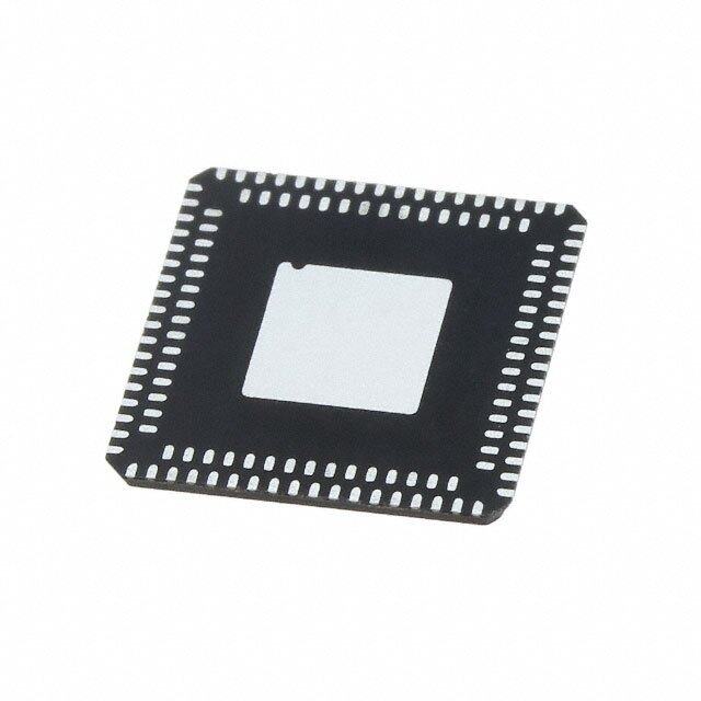
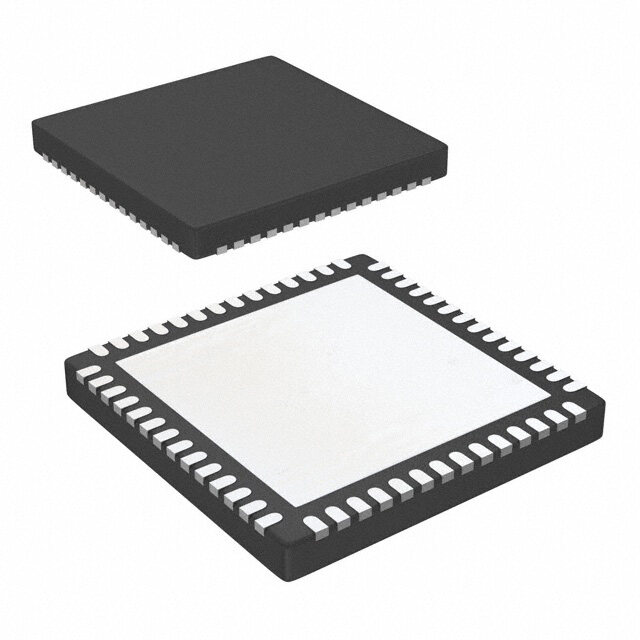
ICGOO电子元器件商城为您提供PCA9663B,118由NXP Semiconductors设计生产,在icgoo商城现货销售,并且可以通过原厂、代理商等渠道进行代购。 PCA9663B,118价格参考¥26.32-¥28.55。NXP SemiconductorsPCA9663B,118封装/规格:接口 - 控制器, I²C 控制器 I²C 接口 48-LQFP(7x7)。您可以下载PCA9663B,118参考资料、Datasheet数据手册功能说明书,资料中有PCA9663B,118 详细功能的应用电路图电压和使用方法及教程。
型号为PCA9663B,118的器件由NXP USA Inc.生产,属于接口-控制器类别,是一款主要用于工业自动化和通信系统中的协议转换控制器。该芯片主要应用于将RS-232/RS-485等串行通信接口转换为I²C或SMBus接口,从而实现不同通信协议之间的数据交换。

其典型应用场景包括工业现场总线系统、楼宇自动化、远程通信设备以及智能传感器网络等。在这些系统中,PCA9663B,118能够有效协调主控制器与外围设备之间的通信,支持多点通信和地址识别功能,提升系统的集成度与通信效率。

此外,该器件也常用于嵌入式系统中,作为主控单元与外部设备或模块(如ADC、DAC、温度传感器等)之间的通信桥梁。其具备良好的抗干扰能力,适合在电磁环境复杂的工业场合中稳定工作。

综上,PCA9663B,118广泛应用于需要串行通信与I²C/SMBus协议转换的工业控制、通信设备及智能系统中,具备可靠性高、集成度强、通信稳定等特点。
| 参数 | 数值 |
| 产品目录 | 集成电路 (IC) |
| 描述 | IC CONTROLLER 48LQFP |
| 产品分类 | |
| 品牌 | NXP Semiconductors |
| 数据手册 | |
| 产品图片 |
|
| 产品型号 | PCA9663B,118 |
| PCN封装 | |
| rohs | 无铅 / 符合限制有害物质指令(RoHS)规范要求 |
| 产品系列 | - |
| 供应商器件封装 | 48-LQFP(7x7) |
| 其它名称 | 568-7583-2 |
| 功能 | 控制器 |
| 包装 | 带卷 (TR) |
| 协议 | I²C |
| 封装/外壳 | 48-LQFP |
| 工作温度 | -40°C ~ 85°C |
| 接口 | I²C |
| 标准 | - |
| 标准包装 | 2,000 |
| 电压-电源 | 3 V ~ 3.6 V |
| 电流-电源 | 15mA |


- 商务部:美国ITC正式对集成电路等产品启动337调查
- 曝三星4nm工艺存在良率问题 高通将骁龙8 Gen1或转产台积电
- 太阳诱电将投资9.5亿元在常州建新厂生产MLCC 预计2023年完工
- 英特尔发布欧洲新工厂建设计划 深化IDM 2.0 战略
- 台积电先进制程称霸业界 有大客户加持明年业绩稳了
- 达到5530亿美元!SIA预计今年全球半导体销售额将创下新高
- 英特尔拟将自动驾驶子公司Mobileye上市 估值或超500亿美元
- 三星加码芯片和SET,合并消费电子和移动部门,撤换高东真等 CEO
- 三星电子宣布重大人事变动 还合并消费电子和移动部门
- 海关总署:前11个月进口集成电路产品价值2.52万亿元 增长14.8%


PDF Datasheet 数据手册内容提取
PCA9663 Parallel bus to 3 channel Fm+ I2C-bus controller Rev. 1.2 — 14 December 2016 Product data sheet 1. General description The PCA9663 is an advanced single master mode I2C-bus controller. It is a fourth generation bus controller designed for data intensive I2C-bus data transfers. It has three independent I2C-bus channels with data rates up to 1Mbits/s using the Fast-mode Plus (Fm+) open-drain topology. Each channel has a generous 4352byte data buffer which makes the PCA9663 the ideal companion to any CPU that needs to transmit and receive large amounts of serial data. The PCA9663 is a 8-bit parallel-bus to I2C-bus protocol converter. Each channel can be configured to communicate with up to 64slaves in one serial sequence with no intervention from the CPU. The controller also has a sequence loop control feature that allows it to automatically retransmit a stored sequence. Its onboard oscillator and PLL allow the controller to generate the clocks for the I2C-bus and for the interval timer used in sequence looping. This feature greatly reduces CPU overhead when data refresh is required in fault tolerant applications. An external trigger input allows data synchronization with external events. The trigger signal controls the rate at which a stored sequence is re-transmitted over the I2C-bus. Error reporting is handled at the transaction level, channel level and controller level with a simple interrupt tree and interrupt masks allow further customization of interrupt management. The controller and parallel bus interfaces run at 3.3V and the I2C-bus I/Os are 5V tolerant with logic levels referenced to a dedicated V input pin with a range of 3.0V DD(IO) to 5.5V. 2. Features and benefits Parallel-bus to I2C-bus protocol converter and interface 1Mbit/s and up to 30mA SCL/SDA I Fast-mode Plus (Fm+) capability OL Internal oscillator trimmed to 1% accuracy reduces external components Individual 4352-byte buffers for the Fm+ channels for a total of 13056bytes of buffer space Three levels of reset: individual software reset, global software reset, global hardware RESET pin Communicates with up to 64 slaves on each channel in one serial sequence Sequence looping with interval timer Supports SCL clock stretching JTAG port available for boundary scan testing during board manufacturing process Trigger input synchronizes serial communication exactly with external events
PCA9663 NXP Semiconductors Parallel bus to 3 channel Fm+ I2C-bus controller Maskable interrupts Fast-mode Plus I2C-bus capable and compatible with SMBus Operating supply voltage: 3.0V to 3.6V (device and host interface) I2C-bus I/O supply voltage: 3.0V to 5.5V Latch-up testing is done to JEDEC Standard JESD78 which exceeds 100mA ESD protection exceeds 8000V HBM per JESD22-A114, and 1000V CDM per JESD22-C101 Packages offered: LQFP48 3. Applications Add I2C-bus port to controllers/processors that do not have one Add additional I2C-bus ports to controllers/processors that need multiple I2C-bus ports Converts 8bits of parallel data to serial data stream to prevent having to run a large number of traces across the entire printed-circuit board Entertainment systems LED matrix control Data intensive I2C-bus transfers 4. Ordering information Table 1. Ordering info rmation Type number Topside Package marking Name Description Version PCA9663B PCA9663 LQFP48 plastic low profile quad flat package; 48leads; SOT313-2 body771.4mm 4.1 Ordering options Table 2. Ordering opt ions Type number Orderable Package Packing method Minimum Temperature partnumber orderquantity PCA9663B PCA9663B,118 LQFP48 REEL 13" Q1/T1 2000 T =40C to +85C amb *STANDARD MARK SMD PCA9663 All information provided in this document is subject to legal disclaimers. © NXP Semiconductors N.V. 2016. All rights reserved. Product data sheet Rev. 1.2 — 14 December 2016 2 of 68
PCA9663 NXP Semiconductors Parallel bus to 3 channel Fm+ I2C-bus controller 5. Block diagram CE WR RDINT RESET Channel 0 PCA9663 Fm+ I2C-bus control STATUS0_[n] CONTROL SDA0 CHSTATUS SCL0 INTMSK TRIG SLATABLE TRANCONFIG INTERRUPT A0 DATA CONTROL TRANSEL A1 TRANOFS A2 BYTECOUNT 4352-BYTE BUFFER FRAMECNT BUFFER CONTROL A3 REFRATE A4 SCLL BUS A5 SCLH INTERFACE A6 MODE TIMEOUT A7 PRESET D0 Channel 1 Fm+ I2C-bus control D1 STATUS1_[n] D2 CONTROL D3 SDA1 CHSTATUS SCL1 INTMSK D4 SLATABLE CTRLSTATUS D5 TRANCONFIG CTRLINTMSK D6 DATA DEVICE_ID D7 TRANSEL TRANOFS CTRLPRESET BYTECOUNT 4352-BYTE CTRLRDY FRAMECNT BUFFER REFRATE SCLL CONTROL BLOCK SCLH MODE POWER-ON/ TIMEOUT POWER-DOWN VDD PRESET RESET Channel 2 Fm+ I2C-bus control DC/DC STATUS2_[n] REGULATOR CONTROL SDA2 CHSTATUS TCK SCL2 INTMSK TRST SLATABLE JTAG TMS TRANCONFIG TDI DATA TDO TRANSEL TRANOFS BYTECOUNT 4352-BYTE OSCILLATOR FRAMECNT BUFFER VDD(IO) REFRATE SCLL PLL SCLH MODE TIMEOUT PRESET 002aae940 Fig 1. Block diagram PCA9663 All information provided in this document is subject to legal disclaimers. © NXP Semiconductors N.V. 2016. All rights reserved. Product data sheet Rev. 1.2 — 14 December 2016 3 of 68
PCA9663 NXP Semiconductors Parallel bus to 3 channel Fm+ I2C-bus controller 6. Pinning information 6.1 Pinning D S D S D S D S 5 4 D S 3 2 D S 1 0 V V D D V V D D V V D D 8 7 6 5 4 3 2 1 0 9 8 7 4 4 4 4 4 4 4 4 4 3 3 3 D6 1 36 RESET D7 2 35 VSS A0 3 34 TRIG A1 4 33 CE A2 5 32 RD A3 6 31 WR PCA9663B VDD 7 30 VDD VSS 8 29 VSS A4 9 28 SCL0 A5 10 27 SDA0 A6 11 26 SCL1 A7 12 25 SDA1 3 4 5 6 7 8 9 0 1 2 3 4 1 1 1 1 1 1 1 2 2 2 2 2 002aaf692 TRST TMS TCK TDI TDO VDD VSS INT SDA2 SCL2 SS(IO) DD(IO) V V Fig 2. Pin configuration for LQFP48 6.2 Pin description Table 3. Pin description Symbol Pin Type Description A0 3 I Address inputs: selects the bus controller’s internal registers and ports for read/write operations. Address is registered when A1 4 I CE is LOW and whether WR or RD transitions LOW. A0 is the A2 5 I least significant bit. A3 6 I A4 9 I A5 10 I A6 11 I A7 12 I D0 37 I/O Data bus: bidirectional 3-state data bus used to transfer commands, data and status between the bus controller and the D1 38 I/O host. D0 is the least significant bit. Data is registered on the D2 41 I/O rising edge of WR when CE is LOW. D3 42 I/O D4 45 I/O D5 46 I/O D6 1 I/O D7 2 I/O PCA9663 All information provided in this document is subject to legal disclaimers. © NXP Semiconductors N.V. 2016. All rights reserved. Product data sheet Rev. 1.2 — 14 December 2016 4 of 68
PCA9663 NXP Semiconductors Parallel bus to 3 channel Fm+ I2C-bus controller Table 3. Pin description …continued Symbol Pin Type Description TRST 13 I JTAG test reset input. For normal operation, hold LOW (V ). SS TMS 14 I JTAG test mode select input. For normal operation, hold HIGH (V ). DD TCK 15 I JTAG test clock input. For normal operation, hold HIGH (V ). DD TDI 16 I JTAG test data in input. For normal operation, hold HIGH (V ). DD TDO 17 O JTAG test data out output. For normal operation, do not connect (n.c.). INT 20 O Interrupt request: ActiveLOW, open-drain, output. This pin requires a pull-up device. SDA2 21 I/O Channel2 I2C-bus serial data input/output (open-drain). Thispin requires a pull-up device. SCL2 22 I/O Channel2 I2C-bus serial clock input/output (open-drain). This pin requires a pull-up device. SDA1 25 I/O Channel1 I2C-bus serial data input/output (open-drain). Thispin requires a pull-up device. SCL1 26 I/O Channel1 I2C-bus serial clock input/output (open-drain). This pin requires a pull-up device. SDA0 27 I/O Channel0 I2C-bus serial data input/output (open-drain). Thispin requires a pull-up device. SCL0 28 I/O Channel0 I2C-bus serial clock input/output (open-drain). Thispin requires a pull-up device. WR 31 I Write strobe: When LOW and CE is also LOW, the content of the data bus is loaded into the addressed register. Data are latched on the rising edge of WR. CE may remain LOW or transition with WR. RD 32 I Read strobe: When LOW and CE is also LOW, causes the contents of the addressed register to be presented on the data bus. The read cycle begins on the falling edge of RD. Data lines are driven when RD and CE are LOW. CE may transition with RD. CE 33 I Chip Enable: ActiveLOW input signal. When LOW, data transfers between the host and the bus controller are enabled on D0toD7 as controlled by the WR, RD and A0toA7 inputs. When HIGH, places the D0toD7 lines in the 3-state condition. During the initialization period, CE must transition with RD until controller is ready. TRIG 34 I Trigger input: provides the trigger to start a new frame. RESET 36 I Reset: ActiveLOW input. A LOW level resets the device to the power-on state. Internally pulled HIGH through weak pull-up current. V 24 power I/O power supply: 3.0V to 5.5V. Power supply reference for DD(IO) I2C-bus pins. Sets the voltage reference point for V /V . IL IH PCA9663 All information provided in this document is subject to legal disclaimers. © NXP Semiconductors N.V. 2016. All rights reserved. Product data sheet Rev. 1.2 — 14 December 2016 5 of 68
PCA9663 NXP Semiconductors Parallel bus to 3 channel Fm+ I2C-bus controller Table 3. Pin description …continued Symbol Pin Type Description V 23 power I/O supply ground. SS(IO) V 7, 18, 30, power Power supply: 3.0V to 3.6V. All V pins should be connected DD DD 40, 44, 48 together externally. V 8, 19, 29, power Supply ground. All V pins must be tied together externally. SS SS 35, 39, 43, 47 7. Functional description 7.1 General The PCA9663 acts as an interface device between standard high-speed parallel buses and the serial I2C-bus. On the I2C-bus, it acts as a master. Data transfer between the I2C-bus and the parallel-bus host is carried out on a buffered basis, using either an interrupt or polled handshake. 7.2 Internal oscillator and PLL The PCA9663 contains an internal 12.0MHz oscillator and 156MHz PLL which are used for all internal and I2C-bus timing. The oscillator and PLL require up to t to startup init(po) and lock after power-up. The oscillator is not shutdown if the serial bus is disabled. 7.3 Buffer description Remark: In the following section a transaction is defined as a contiguous set of commands and/or data sent/received to/from a single slave. A sequence is a set of transactions stored in the buffer. The PCA9663 channels have individual 4352-byte data buffers (see Section 7.3.2 “Buffer sizes”) that allow several transactions to be executed before an interrupt is generated. This allows the host to request several transactions (up to maximum buffer size on each channel) in a single sequence and lets the PCA9663 perform it without the intervention of the host each time a requested transaction is performed. The host can then perform other tasks while the PCA9663 executes the requested sequences. By following a simple protocol, the I2C-bus controller can store several I2C-bus transactions directed to different slaves addresses on any of the channels. The transaction stored in the buffer can be of any type, thus reads and writes can be interlaced in a sequence. When multiple slave reads are requested in a sequence, the read data is stored in-line in the sequence and the buffer number must be specified in the TRANSEL to provide the read location and the TRANOFS byte offset value. By default, the TRANOFS is set to 00h. So let us consider the scenariowhere the host has done the initialization (mode, masks, and other configuration) and writes data into the buffer of one of the three channels. The host starts by programming the buffer configuration registers TRANCONFIG (number of slaves and bytes per slave) and then the SLATABLE (slave addresses). Then the host programs the TRANSEL (Transaction Data Buffer Selection) and the TRANOFS (byte offset selection) to 00h to set the memory pointers to the beginning of the buffer (the default value is 00h after a power-on or RESET). Next, the host transfers the data into PCA9663 All information provided in this document is subject to legal disclaimers. © NXP Semiconductors N.V. 2016. All rights reserved. Product data sheet Rev. 1.2 — 14 December 2016 6 of 68
PCA9663 NXP Semiconductors Parallel bus to 3 channel Fm+ I2C-bus controller DATA until the entire sequence is loaded. If the transaction is a read transaction, the host must write a dummy byte (i.e., FFh) for each expected serial read byte to reserve the memory space in the buffer for the transaction. Care should be taken so as to not overflow the buffer with excessive read/write commands. In the event of an overflow, represented by the BE bit in the CTRLSTATUS register, will be set to logic1. The INT pin will be set LOW if the BEMSK bit in the CTRLINTMSK register is logic0. To recover the channel, a channel reset is required. All configuration and data needs to be checked by the host and resent to the I2C-bus controller. (See Section 7.3.2 “Buffer sizes”.) After sending all the commands and data it wanted to the I2C-bus controller, the host could either continue to program data for other channels or write to the CONTROL register to begin data transmission on the current channel. The transactions will be sent on the I2C-bus in the order in which the slave addresses are listed in the SLATABLE, separated by a RESTART condition. The last transaction in the sequence will end with a STOP condition. If during a READ command a NACK on the slave address is received, the buffer space allocated for the read will remain untouched and will contain the last information written in that location. A buffer read on the parallel bus should only be done after a valid buffer state is reached to guarantee data valid (see Section 7.5.1.1 “STATUS0_[n], STATUS1_[n], STATUS2_[n] — Transaction status registers”). A buffer write is only allowed during the channel idle state. To program data for another channel, that channel is selected and data programmed as described above. One or more channels can be busy while additional data is sent to the buffer of an idle channel. 7.3.1 Buffer management assumptions • Repeated STARTs will be sent between two consecutive transactions. • After the last operation on a channel is completed, a STOP will be sent. • In a READ transaction, after the last data byte has been received from a particular slave, a NACK is sent to the slave. 7.3.2 Buffer sizes The PCA9663 channels have individual buffers assigned to them. The contents of the buffers should only be modified during channel idle states. The memory allocation is 4352bytes per channel. The buffer sizes represent the memory allocated for the data block only. The slave address table and configuration bytes are contained in other locations and do not need to be included in the required buffer size calculation. For example, to calculate the size of the memory needed to write 26bytes to 10slaves and to read 2bytes from 4slaves (no command bytes required for the read): 10slaves26bytes/slave = 260bytes for the write transactions 4slaves2bytes/slave = 8bytes for the read transactions A total of 268 bytes of buffer space is required to complete the sequence. PCA9663 All information provided in this document is subject to legal disclaimers. © NXP Semiconductors N.V. 2016. All rights reserved. Product data sheet Rev. 1.2 — 14 December 2016 7 of 68
PCA9663 NXP Semiconductors Parallel bus to 3 channel Fm+ I2C-bus controller Remark: Note that the bytes required to store the 30slave addresses are not included in the calculation since they are stored in the SLATABLE register. 7.4 Error reporting and handling In case of any transaction error conditions, the device will load the transaction error status in the STATUSx_[n], generate an interrupt, if unmasked, by pulling down the INT pin and update the CHSTATUS and CTRLSTATUS registers. The status for the individual SLA addresses will be stored in the STATUSx_[n] registers. In the event of a NACK from a slave, there are two possible courses of action. The first is that an interrupt will be generated and the current transaction and sequence terminated. The second is that while the WEMSK and/or REMSK is a logic1, a NACKed byte will be ignored, and the transmission will continue with the next transaction in the sequence until the end of the sequence. The controller will skip the slave address and/or data where the NACK occurred and move on to the next transaction in the sequence. Any error will be reported in the corresponding STATUSx_[n] register (where ‘n’ is the buffer number of the slave) or the CHSTATUS or CTRLSTATUS registers. 7.5 Registers The PCA9663 contains several registers that are used to configure the operation of the device, status reporting, and to send and receive data. The device also contains global registers for chip level control and status reporting. The STATUSx_[n] registers are channel-level direct access registers. The DATA, SLATABLE, TRANCONFIG, and BYTECOUNT registers are auto-increment registers. The memory access pointer to the DATA registers can be programmed using the TRANSEL and TRANOFS registers. See Section 7.5.1.2 “CONTROL — Control register”, for information on the pointer reset bits BPTRRST and AIPTRRST. PCA9663 All information provided in this document is subject to legal disclaimers. © NXP Semiconductors N.V. 2016. All rights reserved. Product data sheet Rev. 1.2 — 14 December 2016 8 of 68
xxxxxxxxxxxxxxxxxxxxx xxxxxxxxxxxxxxxxxxxxxxxxxx xxxxxxx x x x xxxxxxxxxxxxxxxxxxxxxxxxxxxxxx xxxxxxxxxxxxxxxxxxx xx xx xxxxx xxxxxxxxxxxxxxxxxxxxxxxxxxx xxxxxxxxxxxxxxxxxxx xxxxxx xxxxxxxxxxxxxxxxxxxxxxxxxxxxxxxxxxx xxxxxxxxxxxx x x xxxxxxxxxxxxxxxxxxxxx xxxxxxxxxxxxxxxxxxxxxxxxxxxxxx xxxxx xxxxxxxxxxxxxxxxxxxxxxxxxxxxxxxxxxxxxxxxxxxxxxxxxx xxxxxxxx xxxxxxxxxxxxxxxxxxxxxxxxx xxxxxxxxxxxxxxxxxxxx xxx P P N roduct d CA9663 Ta7ble 46. P5CA96463 re3giste2r add1ress0 mapR e- gdiisrteecrt nreagmiseteAr caccecsesss Wwhriitlee access Description Default S(biyzete s) XP S a e ta CHactive m she Channel status registers ic e o t 0 0 channel 0 transaction number STATUS0_[n] R no individual transaction status (direct address) 00h 64 n d (hex) u c 0 1 channel 1 transaction number STATUS1_[n] R no individual transaction status (direct address) 00h 64 t o (hex) r s 1 0 channel 2 transaction number STATUS2_[n] R no individual transaction status (direct address) 00h 64 (hex) Channel 0 (Fm+) registers 1 1 0 0 0 0 0 0 CONTROL R/W yes[1] channel 0 control 00h 1 A ll inform 0 0 0 1 CHSTATUS R no channel 0 status 00h 1 Rev. 1.2 — 14 December 2016 ation provided in this document is subject to legal disclaim 0000001 0011110 1100110 0101100 ISTDTTBNRRRLYATATTAAAMTAENNNASCOSCBKOEOFLLSUNENFTIG RRRRRRR//////WWWWWW yyyynTnyeeeeeooRsssssA, NfoCr OUNT[2] ccccc(c(caahhhhhhhuuaaaaaaattnnnnnnnoonnnnnnn--iieeeeeeennlllllllcc 0000000rree sttdittmmnrrrrlaaaaaateeetnnnnvannrsssse rtta(aamu ))aacccpiudtttttiiitt doooeomrnnnd-eai nsddcbscsoaaykr ntttteaaeafmi bgbbcleuouuenruff aff(tneea)titrruo sbtnoey -ltieenc cotrfefsmeetnt) 00000000000000hhhhhhh 1611b664u45fsize[3] Parallel bu ers. 1 0 0 1 FRAMECNT R/W no channel 0 frame count 01h 1 s t o 1 0 1 0 REFRATE R/W no channel 0 frame refresh rate 00h 1 3 c 1 0 1 1 SCLL R/W no channel 0 clock LOW state 5Eh 1 h a n 1 1 0 0 SCLH R/W no channel 0 clock HIGH state 3Fh 1 n © NXP 1 1 0 1 MODE R/W no channel 0 mode 92h 1 el F Sem 1 1 1 0 TIMEOUT R/W no channel 0 time-out 00h 1 m iconductors N 1 1 1 1 PRESET R/W yes channel 0 parallel reset 00h 1 + IC-b2 PC 9 of 68 .V. 2016. All rights reserved. us controller A9663
xxxxxxxxxxxxxxxxxxxxx xxxxxxxxxxxxxxxxxxxxxxxxxx xxxxxxx x x x xxxxxxxxxxxxxxxxxxxxxxxxxxxxxx xxxxxxxxxxxxxxxxxxx xx xx xxxxx xxxxxxxxxxxxxxxxxxxxxxxxxxx xxxxxxxxxxxxxxxxxxx xxxxxx xxxxxxxxxxxxxxxxxxxxxxxxxxxxxxxxxxx xxxxxxxxxxxx x x xxxxxxxxxxxxxxxxxxxxx xxxxxxxxxxxxxxxxxxxxxxxxxxxxxx xxxxx xxxxxxxxxxxxxxxxxxxxxxxxxxxxxxxxxxxxxxxxxxxxxxxxxx xxxxxxxx xxxxxxxxxxxxxxxxxxxxxxxxx xxxxxxxxxxxxxxxxxxxx xxx P P Table 4. PCA9663 register address map - direct register access …continued N rodu CA9663 7 6 5 4 3 2 1 0 Register name Access Write access Description Default Size XP ct d while (bytes) S a CHactive e ta m sh Channel 1 (Fm+) registers ic e e 1 1 0 1 0 0 0 0 CONTROL R/W yes[1] channel 1 control 00h 1 o t n 0 0 0 1 CHSTATUS R no channel 1 status 00h 1 d u c 0 0 1 0 INTMSK R/W yes channel 1 interrupt mask 00h 1 t o 0 0 1 1 SLATABLE R/W no channel 1 slave address table (auto-increment) 00h 64 r s 0 1 0 0 TRANCONFIG R/W yes, for channel 1 transaction configuration 00h 65 TRANCOUNT[2] (auto-increment) 0 1 0 1 DATA R/W yes channel 1 data (auto-increment) 00h bufsize[3] A 0 1 1 0 TRANSEL R/W yes channel 1 transaction data buffer select 00h 1 ll inform 0 1 1 1 TRANOFS R/W yes channel 1 transaction data buffer byte offset 00h 1 Rev. 1.2 — 14 December 2016 ation provided in this document is subject to legal disclaim 11111111 11100100 01111000 00101110 STPRSMFBIRCRCYEOMTALELFDEHELMRSEOCEAEUTOTCTEUNNTT RRRRRRRR///////WWWWWWW nynnnnnneooooooos ccccccc(cahhhhhhhhuaaaaaaaatnnnnnnnnonnnnnnnn-ieeeeeeeenllllllllc 11111111re ptfcmcftmrirrmllaaaaoooermnmccedanskk-eleetlom )e HL ucrliOe ItotrGtfeeuWrHesdn es t sbshttyta artteatee tceount 030090501F0020E0hhhhhhhh 111111164 Parallel bu ers. s t o 3 c h a n n © NXP el F Sem m iconductors N + IC-b2 PC 10 of 68 .V. 2016. All rights reserved. us controller A9663
xxxxxxxxxxxxxxxxxxxxx xxxxxxxxxxxxxxxxxxxxxxxxxx xxxxxxx x x x xxxxxxxxxxxxxxxxxxxxxxxxxxxxxx xxxxxxxxxxxxxxxxxxx xx xx xxxxx xxxxxxxxxxxxxxxxxxxxxxxxxxx xxxxxxxxxxxxxxxxxxx xxxxxx xxxxxxxxxxxxxxxxxxxxxxxxxxxxxxxxxxx xxxxxxxxxxxx x x xxxxxxxxxxxxxxxxxxxxx xxxxxxxxxxxxxxxxxxxxxxxxxxxxxx xxxxx xxxxxxxxxxxxxxxxxxxxxxxxxxxxxxxxxxxxxxxxxxxxxxxxxx xxxxxxxx xxxxxxxxxxxxxxxxxxxxxxxxx xxxxxxxxxxxxxxxxxxxx xxx P P Table 4. PCA9663 register address map - direct register access …continued N rodu CA9663 7 6 5 4 3 2 1 0 Register name Access Write access Description Default Size XP ct d while (bytes) S a CHactive e ta m sh Channel 2 (Fm+) registers ic e e 1 1 1 0 0 0 0 0 CONTROL R/W yes[1] channel 2 control 00h 1 o t n 0 0 0 1 CHSTATUS R no channel 2 status 00h 1 d u c 0 0 1 0 INTMSK R/W yes channel 2 interrupt mask 00h 1 t o 0 0 1 1 SLATABLE R/W no channel 2 slave address table (auto-increment) 00h 64 r s 0 1 0 0 TRANCONFIG R/W yes, for channel 2 transaction configuration 00h 65 TRANCOUNT[2] (auto-increment) 0 1 0 1 DATA R/W yes channel 2 data (auto-increment) 00h bufsize[3] A 0 1 1 0 TRANSEL R/W yes channel 2 transaction data buffer select 00h 1 ll inform 0 1 1 1 TRANOFS R/W yes channel 2 transaction data buffer byte offset 00h 1 Rev. 1.2 — 14 December 2016 ation provided in this document is subject to legal disclaim 11111111 11100100 01111000 00101110 STPRSMFBIRCRCYEOMTALELFDEHELMRSEOCEAEUTOTCTEUNNTT RRRRRRRR///////WWWWWWW nynnnnnneooooooos ccccccc(cahhhhhhhhuaaaaaaaatnnnnnnnnonnnnnnnn-ieeeeeeeenllllllllc 22222222re ptfcmcftmrirrmllaaaaoooermnmccedanskk-eleetlom )e HL ucrliOe ItotrGtfeeuWrHesdn es t sbshttyta artteatee tceount 030090501F0020E0hhhhhhhh 111111164 Parallel bu ers. s t o 3 c h a n n © NXP el F Sem m iconductors N + IC-b2 PC 11 of 68 .V. 2016. All rights reserved. us controller A9663
xxxxxxxxxxxxxxxxxxxxx xxxxxxxxxxxxxxxxxxxxxxxxxx xxxxxxx x x x xxxxxxxxxxxxxxxxxxxxxxxxxxxxxx xxxxxxxxxxxxxxxxxxx xx xx xxxxx xxxxxxxxxxxxxxxxxxxxxxxxxxx xxxxxxxxxxxxxxxxxxx xxxxxx xxxxxxxxxxxxxxxxxxxxxxxxxxxxxxxxxxx xxxxxxxxxxxx x x xxxxxxxxxxxxxxxxxxxxx xxxxxxxxxxxxxxxxxxxxxxxxxxxxxx xxxxx xxxxxxxxxxxxxxxxxxxxxxxxxxxxxxxxxxxxxxxxxxxxxxxxxx xxxxxxxx xxxxxxxxxxxxxxxxxxxxxxxxx xxxxxxxxxxxxxxxxxxxx xxx P P Table 4. PCA9663 register address map - direct register access …continued N rodu CA9663 7 6 5 4 3 2 1 0 Register name Access Write access Description Default Size XP ct d while (bytes) S a CHactive e ta m sh Global registers ic e e 1 1 1 1 0 0 0 0 CTRLSTATUS R yes controller status 00h 1 o t n 0 0 0 1 CTRLINTMSK R/W yes master interrupt mask 00h 1 d u c 0 0 1 0 - R no reserved 08h t o 0 0 1 1 - R no reserved 00h r s 0 1 0 0 - R no reserved 00h 0 1 0 1 - R no reserved 00h 0 1 1 0 DEVICE_ID R no device ID 63h All inform 01 11 11 11 CCTTRRLLRPRDEYS[4E] T RR/W yneos cmoanstrteorll epra rreaalledly r eresgeitster F00Fhh 11 Rev. 1.2 — 14 December 2016 ation provided in this document is subject to legal disclaim [[[[2413]]]] TCERhxoecenfee ttrrpr oattol nlTe sSPra e rcaectnaitoidodn nyT c =7Eo ..uF3 Cn.F2thh (“a TBinmRugmfAifneeNgrd CspiaOioztleeNalsryFi” tI ayGfo fot[re0 fc r]T )hP PcaOa nwnRnh e boille erm awTefrEtmiet trioes arn ya h tcaoatli lrvdodeucw arwiatniirolgel n ctr.haeeus seidet l oear p fgaellorsiboead tl r birgeegstweeret.. eItn w siellq culeeanrc e(0s0.h) once the initialization routine is done. Parallel bu ers. s t o 3 c h a n n © NXP el F Sem m iconductors N + IC-b2 PC 12 of 68 .V. 2016. All rights reserved. us controller A9663
PCA9663 NXP Semiconductors Parallel bus to 3 channel Fm+ I2C-bus controller 7.5.1 Channel registers 7.5.1.1 STATUS0_[n], STATUS1_[n], STATUS2_[n] — Transaction status registers STATUS0_[n], STATUS1_[n], and STATUS2_[n] are 8-bit64 read-only registers that provide status information for a given transaction. Only the 5 lower bits are used; the topbits will always read 0. When some of these bits are set, a channel interrupt is requested (the INT pin is asserted LOW). A read to STATUSx_[n] register will clear its status. To clear all the STATUSx_[n] registers, a byte-by-byte read of all STATUSx_[n] registers is required. The controller will auto-clear the STATUSx_[n] registers at each START of a sequence when FRAMECNT=1 and only at the first START when FRAMECNT1. Each register byte can be accessed by direct addressing so that the host can choose to read the status on one or more individual transactions without having to read all 64statusbytes. Table 5. STATUSx_[n] - Transaction status code register bit description Bit Symbol Description 7:5 ST[7:5] always reads 000 4 RSN Read slave NACK. When HIGH, a NACK was received after a slave address was transmitted on the serial bus on a read transaction. An interrupt will be requested. 3 WSN Write slave NACK. When HIGH, a NACK was received after a slave address was transmitted on the serial bus on a write transaction. An interrupt will be requested. 2 WDN Write data NACK. When HIGH, a NACK was received for a data byte during a write transaction on the serial bus. An interrupt will be requested. 1 TA Transaction active. When 1, the transaction is currently active on the serial bus. No interrupt is requested. 0 TR Transaction ready. When 1, a transaction is loaded in the buffer and waiting to be executed. No interrupt is requested. Remark: When STATUSx_[n]=00h, no interrupt is requested and the transaction is in the Done/Idle state. During program execution, the TR and TA bits behave as follows: Example, we are to transfer 3 transactions in a sequence. All initialization is completed (loading of SLA, TRANCONFIG, DATA) and device is ready for serial transfer. Before the STA bit is set, the STATUSx_[n] register will contain: STATUSx_[0] = 0 STATUSx_[1] = 0 STATUSx_[2] = 0 STATUSx_[3] = 0 : PCA9663 All information provided in this document is subject to legal disclaimers. © NXP Semiconductors N.V. 2016. All rights reserved. Product data sheet Rev. 1.2 — 14 December 2016 13 of 68
PCA9663 NXP Semiconductors Parallel bus to 3 channel Fm+ I2C-bus controller After STA is set: STATUSx_[0] = 2 STATUSx_[1] = 1 STATUSx_[2] = 1 STATUSx_[3] = 0 : Since there is no timing requirement in setting the STA bit after the initialization, the device will update the first status when the STA bit is set and will always go from 0 to 2 (Idle to Transactionactive). 7.5.1.2 CONTROL — Control register CONTROL is an 8-bit register. The STO bit is affected by the bus controller hardware: it is cleared when a STOP condition is present on the I2C-bus. Table 6. CONTROL - Control register bit description Address: Channel0=C0h; Channel1=D0h; Channel2=E0h. Legend: * reset value Bit Symbol Access Value Description 7 STOSEQ R/W Stop sequence bit. 1 When the STOSEQ bit is set while the channel is active, a STOP condition will be transmitted immediately following the end of the current sequence being transferred on the I2C-bus. No further buffered transactions will be carried out and the channel will return to the idle state. Normal error reporting will occur up until the last bit. When a STOP condition is detected on the bus, the hardware clears the STOSEQ flag. 0 When STOSEQ is reset, no action will be taken. 6 STA R/W The START flag. 1 When the STA bit is set to begin a sequence, the bus controller hardware checks the status of the I2C-bus and generates a START condition if the bus is free. If the bus is not idle, then INT will go LOW and the CHSTATUS register will contain a bus error code (either DAE or CLE will be set). The STA bit may be set only at a valid idle state. The controller will reset the bit under the following conditions: • A sequence is done and FRAMECNT = 1. • A sequence loop is done and FRAMECNT>1. • The STOSEQ bit is set, FRAMECNT = 0, and the current sequence is done. • The STOSEQ bit is set, FRAMECNT>1, and the current sequence is done. • The STO bit is set and the current byte transaction is done. This bit cannot be set if the CHEN bit is 0. 0 When the STA bit is reset, no START condition will be generated. 5 STO R/W The STOP flag. 1 When the STO bit is set while the channel is active, a STOP condition will be transmitted immediately following the current data or slave address byte being transferred on the I2C-bus. If a read is in progress, a NACK will be generated before the STOP. No further buffered transactions will be carried out and the channel will return to the idle state. Normal error reporting will occur up until the last bit. When a STOP condition is detected on the bus, the hardware clears the STO flag. 0 When the STO bit is reset, no action will be taken. PCA9663 All information provided in this document is subject to legal disclaimers. © NXP Semiconductors N.V. 2016. All rights reserved. Product data sheet Rev. 1.2 — 14 December 2016 14 of 68
PCA9663 NXP Semiconductors Parallel bus to 3 channel Fm+ I2C-bus controller Table 6. CONTROL - Control register bit description …continued Address: Channel0=C0h; Channel1=D0h; Channel2=E0h. Legend: * reset value Bit Symbol Access Value Description 4 TP R/W Trigger polarity bit. Cannot be changed while channel is active. 1 Trigger will be detected on a falling edge. 0 Trigger will be detected on a rising edge. 3 TE R/W Trigger Enable (TE) bit controls the trigger input used for frame refresh. TE cannot be changed while channel is active. When the trigger input is enabled, the trigger will override the contents of the FRAMECNT register and will start triggering when STA bit is set. Thereafter, when a trigger tick is detected, the controller will issue a START command and the stored sequence will be transferred on the serial bus. 1 When TE=1, the sequence is controlled by the Trigger input. 0 When TE=0, the trigger inputs are ignored. 2 BPTRRST W 1 Resets auto increment pointers for BYTECOUNT. Reads back as 0. 1 AIPTRRST W 1 Resets auto increment pointers for SLATABLE and TRANCONFIG. The DATA register auto-increment pointer will be set to the value that corresponds to TRANSEL and TRANOFS registers. Reads back as 0. Remark: To reset the data pointer, write 00h to TRANSEL. 0 - W 0 Reserved. User must write 0 to this bit. Remark: Due to a small latency between setting the STA bit and the ability to detect a trigger pulse, if the STA bit is set simultaneously to an incoming trigger pulse, the pulse will be ignored and the controller will wait for the next trigger to send the START. If the STO or STOSEQ bit are set at anytime while the STA bit is 0, then no action will be taken and the write to these bits is ignored. Remark: STO has priority over STOSEQ. PCA9663 All information provided in this document is subject to legal disclaimers. © NXP Semiconductors N.V. 2016. All rights reserved. Product data sheet Rev. 1.2 — 14 December 2016 15 of 68
PCA9663 NXP Semiconductors Parallel bus to 3 channel Fm+ I2C-bus controller Table 7. CONTROL re gister bits STA, STO, STOSEQ operation/behavior Channel state Next write action by host Results (initializationsteps) FRAMECNT TE STA STO STOSEQ Idle (reset, TRANCONFIG, 1 0 0 X X No action. SLATABLE, DATA, STA=0) 1 0 1 X X START transmitted on serial bus followed by sequence stored in buffer. Active (reset, load 1 0 X 0 X No change; cannot write STA while active. TRANCONFIG, SLATABLE, 1 0 X 1 X When the STO bit is set, two actions are DATA, STA=1 possible: 1. If the transaction is a read, a STOP is sent after the first read byte (NACK sent) and the byte count is updated. 2. If the transaction is a write, a STOP is sent after the end of ACK cycle of the current byte and BYTECNT is updated. The SD bits will be set. REFRATE Loop idle (reset, 1 0 0 X X No action. load TRANCONFIG, 1 0 X 0 1 Channel will go immediately to the inactive SLATABLE, DATA STA=1)[1] state and SD and FLD bits will be set.[2] 1 0 X 1 X Channel will go immediately to the inactive state and SD and FLD bits will be set.[2] REFRATE Loop active (reset, 1 0 X 0 0 No action. load, TRANCONFIG, 1 0 X 0 1 STOP at end of current frame. The SD and SLATABLE, DATA, STA=1) FLD bits will be set. 1 0 X 1 X When the STO bit is set, two actions are possible: 1. If the transaction is a read, a STOP is sent after the first read byte (NACK sent) and the byte count is updated. 2. If the transaction is a write, a STOP is sent after the end of ACK cycle of the current byte and BYTECNT is updated. The SD and FLD bits will be set. Trigger Loop Idle (reset, load X 1 0 X X No action. TRANCONFIG, SLATABLE, X 1 X 0 1 STOP at end of current frame. The SD and DATA, STA=1) FLD bits will be set. X 1 X 1 X When the STO bit is set, two actions are possible: 1. If the transaction is a read, a STOP is sent after the first read byte (NACK sent) and the byte count is updated. 2. If the transaction is a write, a STOP is sent after the end of ACK cycle of the current byte and the BYTECNT is updated. The SD and FLD bits will be set. PCA9663 All information provided in this document is subject to legal disclaimers. © NXP Semiconductors N.V. 2016. All rights reserved. Product data sheet Rev. 1.2 — 14 December 2016 16 of 68
PCA9663 NXP Semiconductors Parallel bus to 3 channel Fm+ I2C-bus controller Table 7. CONTROL register bits STA, STO, STOSEQ operation/behavior …continued Channel state Next write action by host Results (initializationsteps) FRAMECNT TE STA STO STOSEQ Trigger Loop active (reset, load X 1 X 0 0 No action. TRANCONFIG, SLATABLE, X 1 X 0 1 Channel will go immediately to the inactive DATA, STA=1) state and SD and FLD bits will be set.[2] X 1 X 1 X Channel will go immediately to the inactive state and SD and FLD bits will be set.[2] [1] Loop Idle is defined as the time elapsed from a STOP to the START of the next sequence while STA=1. [2] Channel Active is defined by the CTRLSTATUS[5:3] bits. 7.5.1.3 CHSTATUS — Channel status register CHSTATUS is an 8-bit read-only register that provides status information for a given channel. Some of these status bits are error codes that cannot be masked (NMI) by the INTMSK register and need attention from the host. All these status drive the INT pin activeLOW. To clear the individual channel interrupt request, you must read the CHSTATUS register. The BE interrupt is cleared by reading the CTRLSTATUS register. After the CHSTATUS register is cleared, only new errors or status updates will cause the CHSTATUS bits to be set. Table 8. CHSTATUS - Channel and buffer status codes register bit description Address: Channel0=C1h; Channel1=D1h; Channel2=E1h. Bit Symbol Description 7 SD Sequence Done. The sequence loaded in the buffer was sent and STOP issued on the serial bus. 6 FLD Frame Loop Done. The FRAMECNT value has been reached. A STOP has been issued on the bus. 5 WE Write Error detected in transaction. An SLA NACK or data NACK was detected in a write transaction of the sequence. 4 RE Read Error detected in transaction. An SLA NACK was detected in a read transaction of the sequence. 3 DAE Bus error, SDA stuck LOW. 2 CLE Bus error, SCL stuck LOW. 1 SSE Bus error, illegal START or STOP detected. 0 FE Frame Error detected. The time required to send the sequence exceeds refresh rate programmed to the REFRATE register or the time between trigger ticks. The DAE, CLE and SSE bits correspond to bus error states, and the FE bit corresponds to host programming errors. DAE - SDA error bit: This bit indicates that the SDA line is stuck LOW when the PCA9663 is trying to send a START condition. CLE - SCL error bit: This bit indicates that the SCL line is stuck LOW. SSE - illegal START/STOP detected bit: This bit indicates that a bus error has occurred during a serial transfer. A bus error is caused when a START or STOP condition occurs at an illegal position in the format frame. Examples of such illegal positions are during the serial transfer of an address byte, a data byte, or an acknowledge bit. A bus error may also be caused when external interference disturbs the internal PCA9663 signals. PCA9663 All information provided in this document is subject to legal disclaimers. © NXP Semiconductors N.V. 2016. All rights reserved. Product data sheet Rev. 1.2 — 14 December 2016 17 of 68
PCA9663 NXP Semiconductors Parallel bus to 3 channel Fm+ I2C-bus controller FE - Frame Error bit: This bit indicates that the time required to send the sequence exceeds the refresh rate programmed in the REFRATE register or the time between trigger ticks. Solving frame errors include programming longer refresh rates, speeding up the bus frequency, shortening the amount of bytes sent/received in the sequence, or increasing the time between trigger ticks. If the frame error is masked by the FEMSK, the device will continue to transmit transactions until the end of the sequence without re-starting the sequence even if new triggers are detected. The total number of sequences transmitted will be the number stored in the FRAMECNT register. Once a complete sequence is transmitted, a new sequence will initiate when a subsequent trigger appears. The FE flag will be held HIGH and sequences will still be transmitted unless CHSTATUS is read. If the frame error is unmasked, the sequence will be aborted at the next logical stopping point (i.e., for a read transaction a NACK will be sent), a STOP transmitted and an interrupt will be generated. Since the controller terminates the sequence in a controlled mechanism, there may be a 2-byte delay if a frame error (FE) is detected during a read transaction. The FE bit is set after the STOP is detected on the bus. sequence A sequence A sequence A time 10 ms 10 ms 10 ms 002aaf247 a. Sequence fully executed within the period programmed in REFRATE register frame error detected, data not sent after FE sequence B time 10 ms 10 ms 10 ms 002aaf627 This condition causes a frame error and the FE bit to be set. b. Sequence exceeds period programmed in REFRATE register, FEMSK=0 frame error detected, FEMSK = 1, data sent after FE sequence C sequence C time 10 ms 10 ms 10 ms 002aaf628 c. Sequence exceeds period programmed in REFRATE register, FEMSK=1 Fig 3. Frame Error detection PCA9663 All information provided in this document is subject to legal disclaimers. © NXP Semiconductors N.V. 2016. All rights reserved. Product data sheet Rev. 1.2 — 14 December 2016 18 of 68
PCA9663 NXP Semiconductors Parallel bus to 3 channel Fm+ I2C-bus controller Table 9. Error detecti on operation/behavior Channel state AR (MODE Error detected Next Action register) (CHSTATUS DAE CLE SSE Active or idle X 0 0 1 Interrupt set, if a transaction is active it will be immediately aborted and no further action taken by controller. Host to re-initialize bus (i.e., force a bus recovery), reset slaves, or take other appropriate recovery action. After bus is recovered, hostto re-start transaction. Active or idle, time-out X 0 1 0 Interrupt set, active transaction will be immediately aborted enabled, and clock line is and no further action taken by controller. No bus recovery LOW possible by bus-controller. Host to recover bus by resetting slaves or system. After bus is recovered, host to re-start transaction. Active and at a START or 1 0 0 0 Interrupt not set, active transaction will be immediately repeated-START condition aborted and a bus recovery will be attempted by the bus-controller. If successful, a start will be issued automatically and the serial transfer will continue normally at the location of the failed transaction. No host action is required. 1 1 0 0 Interrupt set, an auto-recovery was attempted and failed. Active transaction will be immediately aborted and the bus-controller determines bus recovery actions, for example setting the BR bit or resetting the slaves. 0 1 0 0 Interrupt set, active transaction will be immediately aborted and no bus recovery will be attempted by the bus-controller. Host may attempt a bus recovery by setting the BR bit or determine other bus recovery action. 7.5.1.4 INTMSK — Interrupt mask register Through the INTMSK register, there is the option to manage which states generate an interrupt, allowing more control from the host on the transaction. The interrupt mask applies to all transactions in a given channel. A bit set to 1 indicates that the mask is active. The INTMSK register default is all interrupts are un-masked (00h). Table 10. INTMSK - Interrupt mask register bit description Address: Channel0=C2h; Channel1=D2h; Channel2=E2h. Bit Symbol Description 7 SDMSK Sequence Done Mask. The end of sequence interrupt will not be generated. 6 FLDMSK Frame loop done mask. A frame loop done interrupt will not be generated. The controller will enter the idle state. 5 WEMSK Write Error Mask. An SLA NACK or data NACK interrupt will not be generated and the controller will skip the remaining write data in the transaction and continue with the START of the next transaction in the sequence. 4 REMSK Read Error detected in transaction. An SLA NACK interrupt will not be generated and the controller will skip the read transaction and continue with the START of the next transaction in the sequence. 3:1 - reserved 0 FEMSK Frame Error Mask. A frame error interrupt will not be generated. Remark: Use caution and good judgement when using this mask. Unexpected/erratic behavior may result in the slave devices. PCA9663 All information provided in this document is subject to legal disclaimers. © NXP Semiconductors N.V. 2016. All rights reserved. Product data sheet Rev. 1.2 — 14 December 2016 19 of 68
PCA9663 NXP Semiconductors Parallel bus to 3 channel Fm+ I2C-bus controller 7.5.1.5 SLATABLE — Slave address table register SLATABLE is an 8-bit64 register set that makes up a table that stores the slave address for each transaction in the sequence. The table is loaded by using an auto-increment pointer that is not user-accessible. To reset the pointer, the AIPTRRST bit must be set in the CONTROL register. The slave addresses in the SLATABLE register are stored with a zero-based (N1) index. The first slave address occupies the 00h position. Remark: Slave address entries greater than the transaction count are not part of the sequence. TRANCONFIG[0] contains the transaction count that will be included in the sequence. Table 11. SLATABLE - Slave address table register bit description Address: Channel0=C3h; Channel1=D3h; Channel2=E3h. Bit Symbol Description 7:1 SLATABLE[7:1] Slave address. 0 SLATABLE[0] When 1, a read transaction is requested. When 0, a write transaction is requested. T able 12. Example of SLATABLE registers Transaction Slave address 00h 10h 01h 12h 02h 28h 03h 40h 04h 14h : : 3Fh 36h PCA9663 All information provided in this document is subject to legal disclaimers. © NXP Semiconductors N.V. 2016. All rights reserved. Product data sheet Rev. 1.2 — 14 December 2016 20 of 68
PCA9663 NXP Semiconductors Parallel bus to 3 channel Fm+ I2C-bus controller 7.5.1.6 TRANCONFIG — Transaction configuration register The TRANCONFIG register is an 8-bit65 register set that makes up a table that contains the number of transactions that will be executed in a sequence and the number of data bytes involved in the transaction. The first byte of the register is the Transaction Count register. The remaining 64 registers are the Transaction Length registers. Table 13. TRANCONFIG, byte0 - Transaction configuration register bit description Address: Channel0=C4h; Channel1=D4h; Channel2=E4h. Bit Symbol Description 7:0 Number of transactions in the sequence. Maximum is 40h. T able 14. TRANCONFIG, byte1to40h - Transaction configuration register bit description Bit Symbol Description 7:0 Number of bytes per transaction in the sequence. Maximum is FFh. T able 15. Example of TRANCONFIG register loaded Register Value Description Transaction count 10h 16 transactions = 16 slave addresses in the SLATABLE Transaction length 00h 0Ah 10byte transaction Transaction length 01h 12h 18byte transaction Transaction length 02h 28h 40byte transaction Transaction length 03h 40h 64byte transaction : : : Transaction length 3Fh 12h 18byte transaction Remark: Even if the Transaction length (TRANCONFIG[1:40h]) and the SLATABLE([0:3Fh]) are fully initialized, only the specified number of transactions in the Transaction count (TRANCONFIG[0]) will be part of the sequence. If the Transaction count is 0, then there will be no activity on the serial bus if the STA bit is set. In addition, there will be no interrupts generated or status updated. The controller will simply reset the CONTROL.STA bit without performing any transactions. If the Transaction length is 0, a read transaction will be skipped and a write transaction will send the slave address plus write bit (SLA+W) on the serial bus with no data bytes. 7.5.1.7 DATA — I2C-bus Data register DATA is an 8-bit read/write, auto-increment register. It is the interface port to the channel buffer. When accessing the buffer, the host writes a byte of serial data to be transmitted or reads bytes that have just been received at this location. The host can read from the DATA at any time and can only write to this 8-bit register while the channel is idle. Remark: Reading the DATA when the serial interface is active may return outdated or erroneous data. The host can read or write data up to the amount of memory space allotted to the channel. The location at which the data is accessed is stored in the TRANSEL and TRANOFS register (both default at 00h). PCA9663 All information provided in this document is subject to legal disclaimers. © NXP Semiconductors N.V. 2016. All rights reserved. Product data sheet Rev. 1.2 — 14 December 2016 21 of 68
PCA9663 NXP Semiconductors Parallel bus to 3 channel Fm+ I2C-bus controller To return to the data location pointed by the contents of the TRANSEL and TRANOFS register after read or write access to the DATA register, set the AIPTRRST (auto-increment pointer reset) bit in the control register. To return to the first DATA register location in the buffer set the TRANSEL to 00h. Table 16. DATA - Data register bit description Address: Channel0=C5h; Channel1=D5h; Channel2=E5h. Bit Symbol Description 7:0 D[7:0] Eight bits to be transmitted or just received. A logic1 in DATA corresponds to a HIGH level on the I2C-bus. A logic0 corresponds to a LOW level on the bus. 7.5.1.8 TRANSEL — Transaction data buffer select register The TRANSEL register is used to select the pointer to a specific transaction in the DATA buffer. This allows the user to update the data of a specific slave without having to re-write the entire data buffer or to read back the stored serial data from a read transaction. The value of this register is the slave address position in the SLATABLE register. The TRANSEL register is zero-based (N1) register. For example, if a change to the 22nd slave address data is required, the host would set the TRANSEL register to 15h. This register can be used in conjunction with the TRANSOFS register to access a specific byte in the data buffer. The host would then proceed to write the new data to the DATA register. The auto-increment feature continues to operate from this new position in the DATA register. Setting TRANSEL to an uninitialized TRANCONFIG entry may cause a request to read/write data outside the data buffer. If this occurs, the BE bit in the CTRLSTATUS register will be set to a logic1. Write data will be ignored and read data will be invalid. When a new transaction is selected by programming the TRANSEL registers, the TRANSOFS register will automatically be reset to 00h. Remark: When updating the data buffer, if the number of bytes to be updated or read exceeds the number of bytes that were specified in the TRANCONFIG register, the auto-increment will go over the transaction boundary into the next transaction stored in the buffer. Remark: To reset the DATA pointer, write 00h to the TRANSEL register. Table 17. TRANSEL - Transaction data buffer select register bit description Address: Channel0=C6h; Channel1=D6h; Channel2=E6h. Bit Symbol Description 7 - Reserved. 6 - Reserved. 5:0 TRANSEL[5:0] Slave address position in the SLATABLE. The maximum number is 3Fh. PCA9663 All information provided in this document is subject to legal disclaimers. © NXP Semiconductors N.V. 2016. All rights reserved. Product data sheet Rev. 1.2 — 14 December 2016 22 of 68
PCA9663 NXP Semiconductors Parallel bus to 3 channel Fm+ I2C-bus controller 7.5.1.9 TRANOFS — Transaction data buffer byte select register In conjunction with the TRANSEL register, the TRANOFS register is used to select the pointer to a specific byte in a transaction in the data buffer. This allows the user to read or re-write a specific data byte of a specific slave without having to read/re-write the entire data buffer. The TRANOFS register is zero-based (N1), so the maximum bytes this register will point to is 256. For example, if the tenth byte in the 40th slave address data is required, the host would set the TRANSEL register to 27h and the TRANSOFS register to 09h. The host would then proceed with a read to the DATA register. Setting TRANOFS to a byte offset outside of the data buffer will cause the BE bit in the CTRLSTATUS register will be set to a logic1. Write data will be ignored and read data will be invalid. Remark: The number of bytes to be updated or read should not exceed the number of bytes that were specified in the TRANCONFIG register. Doing so will cause the auto-increment to go over the transaction boundary into the next transaction stored in the buffer. Table 18. TRANOFS - Transaction data buffer byte select register bit description Address: Channel0=C7h; Channel1=D7h; Channel2=E7h. Bit Symbol Description 7:0 TRANOFS[7:0] Byte index for the specified transaction buffer in TRANSEL. 7.5.1.10 BYTECOUNT — Transmitted and received byte count register The BYTECOUNT register stores the number of bytes that have been sent or received. The count is continuously updated, therefore the BYTECOUNT is a real time reporting of transmitted and received bytes. This is a read-only register. The BYTECOUNT includes only the bytes that have been ACKed in a write transaction and all bytes received in a read transaction including in transactions where the WEMSK or REMSK are enabled and part or complete transactions have been skipped (see Figure9). The BYTECOUNT register is cleared at the START of every sequence. Table 19. BYTECOUNT, byte0 - Transaction configuration register bit description Address: Channel0=C8h; Channel1=D8h; Channel2=E8h. Bit Symbol Description 7:0 BYTECOUNT[7:0] Number of bytes sent/received per transaction in the sequence. Maximum is FFh. 7.5.1.11 FRAMECNT — Frame count register Table 20. FRAMECNT - Frame count register bit description Address: Channel0=C9h; Channel1=D9h; Channel2=E9h. Bit Symbol Description 7:0 FRAMECNT[7:0] Bit7 to bit0 indicate the number of times buffered commands are to be re-transmitted. Default is 01h. This register is a read/write register. The contents of this register holds the programmed value by the host and is not a real-time count of frames sent on the serial bus. If the FRAMECNT is 00h, the sequence stored in the buffer will loop continuously. A STOP will be sent at the end of each sequence. PCA9663 All information provided in this document is subject to legal disclaimers. © NXP Semiconductors N.V. 2016. All rights reserved. Product data sheet Rev. 1.2 — 14 December 2016 23 of 68
PCA9663 NXP Semiconductors Parallel bus to 3 channel Fm+ I2C-bus controller If the FRAMECNT is 01h, it is defined as the default state and the sequence stored in the buffer will be sent once and a STOP will be sent at the end of the sequence. If the FRAMECNT is greater than 01h, the sequence stored in the buffer will loop FRAMECNTtimes and a STOP will be sent at the end of each sequence. Remark: The FRAMECNT can only be set to loop on the sequence stored in the buffer. 7.5.1.12 REFRATE — Refresh rate register The REFRATE register defines the time period between each sequence start when REFRATE looping is enabled (FRAMECNT1, and TE=0). The refresh period defined by REFRATE should always be programmed to be greater than the time it takes for the sequence to be transferred on the I2C-bus. If the REFRATE values is too small, the frame error (FE) bit will be set and an interrupt will be requested. Table 21. REFRATE - Refresh rate register bit description Address: Channel0=CAh; Channel1=DAh; Channel2=EAh. Bit Symbol Description 7:0 REFRATE[7:0] Bit7 to bit0 indicate the sequence refresh period. The resolution is 100s. The default value is 00h, the timer is disabled, and the sequences will be sent back-to-back if the FRAMECNTis=0 or FRAMECNT is >1. Remark: If the FRAMECNT is 1, then the refresh rate function will be disabled. 7.5.1.13 SCLL, SCLH — Clock rate registers Table 22. SCLL - Clock Rate Low register bit description (Standard-mode, Fast-mode, Fast-mode Plus) Address: Channel0=CBh; Channel 1 = DBh; Channel 2 = EBh. Bit Symbol Description 7:0 L[7:0] Eight bits defining the LOW state of SCL. Default: 94 (5Eh). Table 23. SCLH - Clock Rate High register bit description (Standard-mode, Fast-mode, Fast-mode Plus) Address: Channel0=CCh; Channel 1 = DCh; Channel 2 = ECh. Bit Symbol Description 7:0 H[7:0] Eight bits defining the HIGH state of SCL. Default: 63 (3Fh). The clock rate register for the Standard-mode, Fast-mode, and Fast-mode Plus (Fm+) is controlled by the SCLL and SCLH registers. They define the data rate for the serial bus of the PCA9663. The actual frequency on the serial bus is determined by t (time where HIGH SCL is HIGH), t (time where SCL is LOW), t (rise time), and t (fall time) values. LOW r f Writing illegal values into the SCLL and SCLH registers will cause the part to operate at the respective maximum channel frequency. For Standard, Fast, and Fast-mode Plus, t and t are calculated based on the HIGH LOW values that are programmed into SCLH and SCLL registers and the PLL clock frequency. Remark: The MODE register needs to be programmed before programming the SCLL and SCLH registers in order to know which I2C-bus mode is selected. See Section 7.5.1.14 “MODE — I2C-bus mode register” for more detail. Fast-mode Plus (Fm+) is the default selected mode at power-up or after reset. PCA9663 All information provided in this document is subject to legal disclaimers. © NXP Semiconductors N.V. 2016. All rights reserved. Product data sheet Rev. 1.2 — 14 December 2016 24 of 68
PCA9663 NXP Semiconductors Parallel bus to 3 channel Fm+ I2C-bus controller The clock is derived from the internal PLL frequency which is set at 156MHz (13 OSC clock). Given a 1% accuracy on the internal clock, the worst case T is PLL 1 1 ---------------------------------------- = ------------------------------- = 6.347 ns . 12.12 MHz13 157.56 MHz Calculating clock settings for Standard, Fast, and Fast-mode Plus: 1 TOTAL_SCLLH = -----------------------------scale factor (1) T freq PLL The scale factor is set by the MODE register and used in the TOTAL_SCLLH calculation. The scale factor is 8 for Standard-mode, 4 for Fast-mode, and 1 for Fast-mode Plus. The SCLL and SCLH can be found by: SCLL = 0.6TOTAL_SCLLH (2) SCLH = 0.4TOTAL_SCLLH (3) Remark: The contributions for the rise time (t) and fall time (t) are adjusted internally by r f hardware to match the desired frequency. If an invalid number is written to SCLL or SCLH such that it violates the specification, then the controller will adjust the bus frequency to the allowable SCLL and SCLH minimums. Sample resulting SCL frequencies: Table 24. SCL frequencies I2C-bus mode Frequency Scale factor Standard 100kHz 8 Fast 400kHz 4 Fast-mode Plus 1000kHz 1 T able 25. Typical SCL frequencies Data shown under following conditions: Pull-up resistor R =500; bus capacitance C =~170pF. PU b Desired frequency (kHz) Actual frequency (kHz) SCLL SCLH Standard-mode (Sm) 100 99.3 116 79 90 90.0 129 87 80 80.0 145 98 70 69.5 168 112 60 59.7 194 132 50 50.0 233 156 PCA9663 All information provided in this document is subject to legal disclaimers. © NXP Semiconductors N.V. 2016. All rights reserved. Product data sheet Rev. 1.2 — 14 December 2016 25 of 68
PCA9663 NXP Semiconductors Parallel bus to 3 channel Fm+ I2C-bus controller Table 25. Typical SCL frequencies …continued Data shown under following conditions: Pull-up resistor R =500; bus capacitance C =~170pF. PU b Desired frequency (kHz) Actual frequency (kHz) SCLL SCLH Fast-mode (Fm) 400 398.4 58 39 350 348.7 66 45 300 298.2 78 52 250 250.2 93 62 200 198.0 117 79 150 150.1 155 104 100 100.0 233 156 Fast-mode Plus (Fm+) 1000 999.0 90 63 900 900.0 100 70 800 798.3 113 79 700 698.5 130 90 600 599.9 152 105 500 499.5 183 126 400 399.7 229 158 Remark: The correct MODE setting should be programmed based on desired frequency since the bus controller will internally select the appropriate t and t for the selected mode. r f The minimum I2C-bus frequency is 50kHz. Remark: The actual SCL frequency will be affected by the PLL frequency and the bus load. The controller will adjust the SCL timing by monitoring the rise time on the SCL line and bring the output frequency as close to the programmed value as possible without violating the I2C-bus specification for minimum clock HIGH and LOW timing. PCA9663 All information provided in this document is subject to legal disclaimers. © NXP Semiconductors N.V. 2016. All rights reserved. Product data sheet Rev. 1.2 — 14 December 2016 26 of 68
PCA9663 NXP Semiconductors Parallel bus to 3 channel Fm+ I2C-bus controller 7.5.1.14 MODE — I2C-bus mode register MODE is a read/write register. It contains the control bits that select the bus recovery options, and the correct timing parameters. Timing parameters involved with AC[1:0] are t , t , t , t , t , t . The auto recovery and bus recovery bits are BUF HD;STA SU;STA SU;STO HIGH LOW contained in this register. They control the bus recovery sequence as defined in Section 8.5.1 “I2C-bus obstructed by a LOW level on SDA (DAE)”. Table 26. MODE - I2C-bus mode register bit description Address: Channel0=CDh; Channel1=DDh; Channel2=EDh. Bit Symbol Description 7 CHEN Channel Enable bit. R/W. 0: Channel is disabled, SCL and SDA high-impedance. All registers are accessible for setup and configuration, however a sequence cannot be started if the CHEN bit is 0 (STA cannot be set). 1 (default): Channel is enabled. 6 - Reserved. 5 BR Bus Recovery. When BR is set to 1, the bus controller will attempt a bus recovery by sending 9 clock pulses on the bus. Once the bus recovery is complete, the controller will reset the bit to 0. This bit is not intended to generate random or asynchronous 9clockpulses on the bus. This function is performed automatically when the AR bit is 1. 4 AR Auto Recovery. When AR = 1 (default), the bus controller will automatically attempt to recover the bus as described in Section 8.5.1 “I2C-bus obstructed by a LOW level on SDA (DAE)”. When AR = 0, the bus controller will abort the current transaction and generate an error code by setting the DAE bit in the CHSTATUS register and pulling the INT pin LOW. 3:2 - Reserved. 1:0 AC[1:0] I2C-bus mode selection to ensure proper timing parameters (see Table27 and Table38). AC[1:0]=00: Standard-mode AC parameters selected. AC[1:0]=01: Fast-mode AC parameters selected. AC[1:0]=10 (default): Fast-mode Plus AC parameters selected. AC[1:0]=11: Reserved. Remark: CHEN bit value must be changed only when the I2C-bus is idle. Remark: Change from an I2C-bus mode to a slower one (Fast-mode to Standard-mode, for example) will cause the HIGH and LOW timings of SCL to be violated. It is then required to program the SCLL and SCLH registers with values in accordance with the selected mode. PCA9663 All information provided in this document is subject to legal disclaimers. © NXP Semiconductors N.V. 2016. All rights reserved. Product data sheet Rev. 1.2 — 14 December 2016 27 of 68
PCA9663 NXP Semiconductors Parallel bus to 3 channel Fm+ I2C-bus controller Table 27. I2C-bus mode selection example[1] SCLL SCLH I2C-bus frequency Scale AC[1:0] Mode (decimal) (decimal) (kHz)[2] factor 118 79 100 8 00 Standard 59 39 400 4 01 Fast 94 63 1000 1 10 Fast-mode Plus - - - - 11 reserved [1] SCLL and SCLH values in the table also represents the minimum values that can be used for the corresponding I2C-bus mode. Use of lower values will cause the minimum values to be loaded. 1 [2] Using the formula f = ----------------------------------------------------------------------------------------- SCL T SCLL+SCLHsf+t +t PLL r f 7.5.1.15 TIMEOUT — Time-out register TIMEOUT is an 8-bit read/write register. It is used to determine the maximum time that SCL is allowed to be in a LOW logic state before a CLE interrupt is generated. When the I2C-bus interface is operating, TIMEOUT is loaded in the time-out counter at every LOW SCL transition. Table 28. TIMEOUT - Time-out register bit description Address: Channel0=CEh; Channel 1 = DEh; Channel 2 = EEh. Bit Symbol Description 7 TE Time-out enable/disable TE=1: Time-out function enabled TE=0: Time-out function disabled 6:0 TO[6:0] Time-out value. The time-out period = (TIMEOUT[6:0]+1)200s. The time-out value may vary some, and is an approximate value. The Time-out register can be used in the following cases: • When the bus controller wants to send a START condition and the SCL line is held LOW by some other device. Then the bus controller waits a time period equivalent to the time-out value for the SCL to be released. In case it is not released, the bus controller concludes that there is a bus error, sets the CLE bit in the CHSTATUS register, generates an interrupt signal and releases the SCL and SDA lines. • The time-out feature starts every time the SCL goes LOW. If SCL stays LOW for a time period equal to or greater than the time-out value, the bus controller concludes there is a bus error and behaves in the manner described above. When the I2C-bus interface is operating, TIMEOUT is loaded in the time-out counter at every SCL transition. See Section 8.7 “Global reset” for more information. PCA9663 All information provided in this document is subject to legal disclaimers. © NXP Semiconductors N.V. 2016. All rights reserved. Product data sheet Rev. 1.2 — 14 December 2016 28 of 68
PCA9663 NXP Semiconductors Parallel bus to 3 channel Fm+ I2C-bus controller 7.5.1.16 PRESET — I2C-bus channel parallel software reset register Table 29. PRESET - I2C-bus channel parallel software reset register bit description Address: Channel0=CFh; Channel1=DFh; Channel2=EFh. Bit Symbol Description 7:0 PRESET[7:0] Write-only register used during an I2C-bus channel parallel reset command. PRESET is an 8-bit write-only register. Programming the PRESET register allows the user to reset each individual PCA9663 channel under software control. The software reset is achieved by writing two consecutive bytes to this register. The first byte must be A5h while the second byte must be 5Ah. The writes must be consecutive and the values must match A5h and 5Ah. If this sequence is not followed as described, the reset is aborted. The PRESET resets state-machines, registers, and buffer pointers to the default values, zeroes the TRANCONFIG, SLATABLE, BYTECOUNT, and DATA arrays of the respective channel and will not reset the entire chip. The parallel bus remains active while a software reset is active. The user can read the PRESET register to determine when the reset has completed, PRESET returns all 1s when the reset is active and all 0s when complete. 7.5.2 Global registers 7.5.2.1 CTRLSTATUS — Controller status register The CTRLSTATUS register reports the status of the controller, including the interrupts generated by the parallel bus. There are six status bits. When CTRLSTATUS contains 00h, it indicates the idle state and therefore no serial interrupts are requested. The content of this register is continuously updated during the operation of the controller. The lower 3 bits represent the channels that have an interrupt request pending. To clear the individual channel interrupt request, you must read the CHSTATUS register. Bits[5:3] indicate if a channel is currently active or if it is in the idle state. Table 30. CTRLSTATUS - Interrupt status register bit description Address: F0h. Bit Symbol Description 7 BE Buffer Error. A buffer error such as overflow has been detected. 6 - 5 CH2ACT Channel 2 is active. 4 CH1ACT Channel 1 is active. 3 CH0ACT Channel 0 is active. 2 CH2INTP Channel 2 interrupt pending. 1 CH1INTP Channel 1 interrupt pending. 0 CH0INTP Channel 0 interrupt pending. Remark: A global reset will reset all channels and configuration settings. BE - Buffer Error bit: This bit indicates that a buffer error has been detected. For example, a buffer overflow due to the host programming too many bytes will set this bit. A software or hardware reset is necessary to recover from a buffer error. PCA9663 All information provided in this document is subject to legal disclaimers. © NXP Semiconductors N.V. 2016. All rights reserved. Product data sheet Rev. 1.2 — 14 December 2016 29 of 68
PCA9663 NXP Semiconductors Parallel bus to 3 channel Fm+ I2C-bus controller The buffer error may occur when a data location is being read or written to that has not previously been configured by the TRANCONFIG register. The buffer error can occur on a parallel data write or read beyond the buffer capacity, or setting the TRANSEL and TRANOFS pointers beyond the buffer boundary. When the DATA register is loaded with data that goes beyond the capacity of the buffer, the bytes that go over the buffer size will be ignored and a Buffer Error (BE) will be generated. Special case: The BE interrupt is cleared by reading the CTRLSTATUS register. All other interrupts are cleared by reading the respective CHSTATUS register. SD FLD WE RE CH0INTP DAE CLE SSE FE SD FLD WE RE CH1INTP DAE CLE SSE FE SD FLD WE RE CH2INTP DAE CLE SSE FE 002aaf456 Fig 4. PCA9663 status reporting logic PCA9663 All information provided in this document is subject to legal disclaimers. © NXP Semiconductors N.V. 2016. All rights reserved. Product data sheet Rev. 1.2 — 14 December 2016 30 of 68
PCA9663 NXP Semiconductors Parallel bus to 3 channel Fm+ I2C-bus controller 7.5.2.2 CTRLINTMSK — Control Interrupt mask register The CTRLINTMSK masks all interrupts generated by the masked channel. This allows the host MCU to complete other operations before servicing the interrupt without being interrupted by the same channel. Table 31. CTRLINTMSK - Control interrupt mask register bit description Address: F1h. Bit Symbol Description 7 BEMSK Buffer Error Mask. A buffer error interrupt will not be generated. Remark: Use caution and good judgement when using this mask. Unexpected/erratic behavior may result in the slave devices. 6:3 - reserved 2 CH2MSK When this bit is set to 1, all interrupts for the channel will be masked and the INT pin will not be pulled LOW. 1 CH1MSK When this bit is set to 1, all interrupts for the channel will be masked and the INT pin will not be pulled LOW. 0 CH0MSK When this bit is set to 1, all interrupts for the channel will be masked and the INT pin will not be pulled LOW. PCA9663 All information provided in this document is subject to legal disclaimers. © NXP Semiconductors N.V. 2016. All rights reserved. Product data sheet Rev. 1.2 — 14 December 2016 31 of 68
PCA9663 NXP Semiconductors Parallel bus to 3 channel Fm+ I2C-bus controller SD SDMSK WE WEMSK RE REMSK CH0 interrupt FE sources and masks FEMSK CH0MSK FLD FLDMSK DAE CLE SSE SD SDMSK WE WEMSK RE REMSK CH1 interrupt FE sources and masks FEMSK CH1MSK to INT pin FLD FLDMSK BE BEMSK DAE CLE SSE SD SDMSK WE WEMSK RE REMSK CH2 interrupt FE sources and masks FEMSK CH2MSK FLD FLDMSK DAE CLE SSE 002aaf147 Fig 5. PCA9663 interrupt logic 7.5.2.3 DEVICE_ID — Device ID The DEVICE_ID register stores the bus controller part number so it can be identified on the parallel bus. Table 32. DEVICE_ID - Device ID register bit description Address: F6h. Bit Symbol Description 7 U/A Selects PCU or PCA device. 1 = PCU96xx 0 = PCA96xx 6:0 BCD BCD (Binary Coded Decimal) code of the ending 2 digits for ID. Range is 00h to 79h. The code for the PCA9663 is 63h. PCA9663 All information provided in this document is subject to legal disclaimers. © NXP Semiconductors N.V. 2016. All rights reserved. Product data sheet Rev. 1.2 — 14 December 2016 32 of 68
PCA9663 NXP Semiconductors Parallel bus to 3 channel Fm+ I2C-bus controller 7.5.2.4 CTRLPRESET — Parallel software reset register Table 33. CTRLPRESET - Parallel software reset register bit description Address: F7h. Bit Symbol Description 7:0 CTRLPRESET[7:0] Write-only register used during a device parallel reset command. CTRLPRESET is an 8-bit write-only register. Programming the CTRLPRESET register allows the user to reset the PCA9663 under software control. The software reset is achieved by writing two consecutive bytes to this register. The first byte must be A5h while the second byte must be 5Ah. The writes must be consecutive and the values must match A5h and 5Ah. If this sequence is not followed as described, the reset is aborted. 7.5.2.5 CTRLRDY — Controller ready register Table 34. CTRLRDY - Controller ready register bit description Address: FFh. Bit Symbol Description 7:0 CTRLRDY[7:0] Read-only register indicates the internal state of the controller. FFh indicates the controller is initializing, 00h indicates controller is in normal operating mode. CTRLRDY (address FFh) is an 8-bit read-only register. It indicates the internal state of the controller. When the register is FFh, the controller is in the initialization state. The initialization state will be entered at power-up, after a hardware reset, or after a global software reset. The oscillator and the PLL will be initialized only after a Power-On Reset (POR), a hardware reset, or a global software reset (CTRLPRESET). When the register is 00h, the controller is in the normal operating mode. Access while the controller is initializing requires CE pin follow the RD pin transitions to update the state of the controller that is read back. After controller is ready, the CE pin can be held LOW while RD and WR pins transition. See Figure6, Figure7 and Figure8. PCA9663 All information provided in this document is subject to legal disclaimers. © NXP Semiconductors N.V. 2016. All rights reserved. Product data sheet Rev. 1.2 — 14 December 2016 33 of 68
PCA9663 NXP Semiconductors Parallel bus to 3 channel Fm+ I2C-bus controller CE RD DATA FFh FFh 00h initializing ready 002aag095 Fig 6. During initialization, CE must transition with RD at each read operation PCA9663 All information provided in this document is subject to legal disclaimers. © NXP Semiconductors N.V. 2016. All rights reserved. Product data sheet Rev. 1.2 — 14 December 2016 34 of 68
PCA9663 NXP Semiconductors Parallel bus to 3 channel Fm+ I2C-bus controller ADDR read address X read address Y read address Z CE RD DATA address X address Y address Z 002aag096 Fig 7. During normal operation, CE may remain LOW while RD transitions during multiple reads ADDR write address X write address Y write address Z CE WR DATA data X data Y data Z 002aag097 Fig 8. During normal operation, CE may remain LOW while WR transitions during multiple writes 8. PCA9663 operation The PCA9663 is designed to efficiently transmit and receive large amounts of data on a single master bus. There are three major components that compose the architecture of the I2C-bus controller that interact with each other to provide a high throughput and a high level of automation when it conducts transactions: • Slave address table: specifies the address of the slaves on the bus and the direction (read or write). • Transaction configuration: specifies the size of the transaction. • Data buffer: contains the data to be transmitted or received from the slave. These three components are integrated in the PCA9663 to build a sequence. A sequence is a set of read or write transactions and the minimum sequence size is one read or write transaction. Several transactions can be stored in one sequence and be executed without the intervention of the host controller (CPU) through loop control and using the built-in refresh rate timers. The PCA9663 executes transactions in the order they were loaded into the buffer without interrupting the host. Once the end of a sequence is reached, the Sequence Done (SD) bit will be asserted in the CHSTATUS register and the controller will request an interrupt, if SDMSK=0. At this point, the host can reload the buffer with a new sequence or resend the one that is currently loaded in the buffer. When a sequence is in progress, no interrupts are generated unless there is an error when a transaction is conducted. The host will only receive an interrupt when the sequence is done. The PCA9663 will dynamically shift between being a Master PCA9663 All information provided in this document is subject to legal disclaimers. © NXP Semiconductors N.V. 2016. All rights reserved. Product data sheet Rev. 1.2 — 14 December 2016 35 of 68
PCA9663 NXP Semiconductors Parallel bus to 3 channel Fm+ I2C-bus controller Transmitter or a Master Receiver according to the direction bits specified in the SLATABLE. The host has the ability to retrieve stored serial data as soon as a read transaction is done, while the controller carries on the remaining transactions in the sequence. 8.1 Sequence execution Sequences can have transactions of two types: • Write transactions, where the PCA9663 will behave as a Master Transmitter • Read transactions, where the PCA9663 will behave as a Master Receiver Data transfers in each direction are shown in Figure9. This figure contains the following abbreviations: S — START condition SLA — 7-bit slave address R — Read bit (HIGH level at SDA) W — Write bit (LOW level at SDA) A — Acknowledge bit (LOW level at SDA) A — Not acknowledge bit (HIGH level at SDA) Data — 8-bit data byte P — STOP condition In Figure9, circles are used to indicate when a bit is set in the CHSTATUS register. A channel interrupt is not requested when CHSTATUS=00h and the INT pin is not asserted when the interrupt is masked (see Section7.5.2.2). For a successful sequence execution, all three components mentioned above must exist in the memory and must be correctly setup. There are not safeguards against programming incorrect transaction sizes, data buffer lengths, or direction bits. If the transaction length is set to 00h, then only the slave address with direction bit will be transmitted. Once the host has configured the serial port and programmed the TRANCONFIG (number of slaves and bytes per slave), the SLATABLE (slave addresses), TRANSEL (transaction data buffer selection) and the TRANOFS (byte offset selection) and loaded the serial data into the DATA buffer, the sequence is ready to be transmitted. To send the sequence, the host will set the STA bit in the CONTROL register and the controller will immediately send a START on the serial bus. Then, the transactions will be carried out in the order they appear in the SLATABLE, each being separated by a ReSTART command. If the interrupts are unmasked, the serial transfer will be conducted without generating interrupts in between transactions. Once all transactions are successfully completed, the controller will generate a STOP, the SequenceDone bit (SD) will be set in the CHSTATUS and an interrupt will be generated. PCA9663 All information provided in this document is subject to legal disclaimers. © NXP Semiconductors N.V. 2016. All rights reserved. Product data sheet Rev. 1.2 — 14 December 2016 36 of 68
PCA9663 NXP Semiconductors Parallel bus to 3 channel Fm+ I2C-bus controller When the interrupts are unmasked, a NACK on slave address or data (in a write cycle) will terminate the serial transfer, generate a STOP, and the INT pin will be asserted. The host can read the CTRLSTATUS (Controller status register) to determine which channel generated the interrupt, then it can read the CHSTATUS register of the channel and the STATUSx_[n] to determine which slave address caused the error. If the interrupts WEMSK and REMSK are set, then a NACK on slave address or data (in a write cycle) will not terminate the serial transfer, the error will be stored in the STATUSx_[n] register and the serial transfer will continue with the next transaction in the sequence. Once all transactions are completed, the controller will generate a STOP and the SequenceDone bit (SD) and other error bits (WE or RE) will be set in the CHSTATUS and an interrupt will be generated. If the host wants to poll the PCA9663, it can mask all registers including the SD bit and read the CTRLSTATUS, CHSTATUS, STATUSx_[n], and/or the CONTROL registers to determine the state of the controller. PCA9663 All information provided in this document is subject to legal disclaimers. © NXP Semiconductors N.V. 2016. All rights reserved. Product data sheet Rev. 1.2 — 14 December 2016 37 of 68
xxxxxxxxxxxxxxxxxxxxx xxxxxxxxxxxxxxxxxxxxxxxxxx xxxxxxx x x x xxxxxxxxxxxxxxxxxxxxxxxxxxxxxx xxxxxxxxxxxxxxxxxxx xx xx xxxxx xxxxxxxxxxxxxxxxxxxxxxxxxxx xxxxxxxxxxxxxxxxxxx xxxxxx xxxxxxxxxxxxxxxxxxxxxxxxxxxxxxxxxxx xxxxxxxxxxxx x x xxxxxxxxxxxxxxxxxxxxx xxxxxxxxxxxxxxxxxxxxxxxxxxxxxx xxxxx xxxxxxxxxxxxxxxxxxxxxxxxxxxxxxxxxxxxxxxxxxxxxxxxxx xxxxxxxx xxxxxxxxxxxxxxxxxxxxxxxxx xxxxxxxxxxxxxxxxxxxx xxx P P N rodu CA9663 XP ct d S a transactions with WEMSK and REMSK = 0 e ta m sh S SLA 0 W A DATA A S SLA 0 R A DATA A DATA A S SLA 1 W A DATAn A S S SLA n W A DATAn A P ic e e o t n d A P A P A P A P A P A P A P 00h u data available c to be read on t o 01h 01h 08h 04h 10h parallel bus F8h 04h 08h 04h 80h r C0h s 20h 20h 10h 20h 20h 20h 20h transactions with WEMSK and REMSK = 1 A ll inform S SLA 0 W A DATA A S SLA 0 R A DATA A DATA A S SLA 1 W A DATAn A S S SLA n W A DATAn A P Rev. 1.2 — 14 December 2016 ation provided in this document is subject to legal disclaim 01h 01h ffrroomm mslaavsete tro t om20 A08salhhsatveer 20A04hh 02h 11A00hh dtopa atbare aa lrlveeaal i0blda2u bohslne 20A08hh 02h 02h 20A08hh CEA8000000hhhhh Parallel bu ers. STATUSx_[n] register, no interrupt s t o n CHSTATUS register, interrupt requested; interrupt goes LOW at the STOP 3 c h DATA A any number of data bytes and their associated Acknowledge bits a n A last byte is NACK n © NXP 002aag293 el F Sem m iconductors N E80xha:m spelqeu CeHncSeT AdoTnUeS w ciothd enso: errors + IC-b2 PC 38 of 68 .V. 2016. All rights reserved. Fig 9. PCAD000ChhhA::: s9ffrreaa6qmm6u3eee nIlloo2cCooepp ds aaotnnnaddetu sswseei tqqhcuu oaeed nnwccereesit edd ooennrreeo wwriitthh nao r eearrdo ersrror us controller A9663
xxxxxxxxxxxxxxxxxxxxx xxxxxxxxxxxxxxxxxxxxxxxxxx xxxxxxx x x x xxxxxxxxxxxxxxxxxxxxxxxxxxxxxx xxxxxxxxxxxxxxxxxxx xx xx xxxxx xxxxxxxxxxxxxxxxxxxxxxxxxxx xxxxxxxxxxxxxxxxxxx xxxxxx xxxxxxxxxxxxxxxxxxxxxxxxxxxxxxxxxxx xxxxxxxxxxxx x x xxxxxxxxxxxxxxxxxxxxx xxxxxxxxxxxxxxxxxxxxxxxxxxxxxx xxxxx xxxxxxxxxxxxxxxxxxxxxxxxxxxxxxxxxxxxxxxxxxxxxxxxxx xxxxxxxx xxxxxxxxxxxxxxxxxxxxxxxxx xxxxxxxxxxxxxxxxxxxx xxx P P N rodu CA9663 XP ct d S a e ta m sh ic e e o t n number of d slave addresses u to be included c in a sequence to TRANCONFIG DATA r internal memory pointer s SLATABLE - 40h Transaction count 10h Transaction 0, data byte 0 0000h 00h 10h SLAW 00h 01h Transaction 0 length, 1 byte 00h Transaction 1, data byte 0 01h 11h SLAR 01h 05h Transaction 1 length, 5 bytes 00h Transaction 1, data byte 1 02h 40h SLAW 02h 10h Transaction 2 length, 16 bytes 00h Transaction 1, data byte 2 All inform 03:h E0:h SLA:W 03:h 08:h Transaction 3 le:ngth, 8 bytes 0000hh TTrraannssaaccttiioonn 11,, ddaattaa bbyyttee 34 Rev. 1.2 — 14 December 2016 ation provided in this document is subject to legal disclaimers. 333DEFhhh 232030hhh spllauvseSS Sd LLLairAAAdeWWdcRtrieosns bit 333DEFhhhTdtsreihar100reeni058ac sshhhtla ilobacnuvttcsSTTTire osolbaLrrra naaartainAvtrr nnn,aeddseT ssstansda AhaaaapcsrtBeaedccctaoi tttLsdocntmiiirooosErntdaei nnnao pinlsn kenl666ssugen a123 os igtncu rollltt teee phrsi toaennnh eonnagggeqn sctttulhhheeahe,,, nc cn158tgoic6 otmbbeh nbyy. p attyceelnetoessdtues nt ht,e muensmupsaoecrdey AA05452545AA::::::hhhhhh TTTTTTrrrrrraaaaaannnnnnssssssaaaaaaccccccttttttiiiiiioooooonnnnnn 266226,33,,3 ::::::ddd,,, adddaataaattaaattt aa abbb ybbbyytttyyyeeettt ee e101 5071 sameneqdmu weornriytce es d praaetcaaed Parallel bus to : : 3 internal memory pointer c The memory pointers are managed A00h or F00h h a internally by the buffer controller. n 002aaf620 n © NXP el F Sem m iconductors N + IC-b2 PC 39 of 68 .V. 2016. All rights reserved. Fig 10. SSPthCaatAudse9 d6a n6ad3re casosen qafirgueue rcnaotcmioemn b erelnogtscis/kitne ddrsei axaegresr atnhmoatt ; s ashroaew mnnop.t lues sere-qacuceenssciebl elo.aded us controller A9663
PCA9663 NXP Semiconductors Parallel bus to 3 channel Fm+ I2C-bus controller 8.2 Read transactions Many I2C-bus slave devices need a command or register offset to setup a read operation. In this case, a read transaction is actually a multi-part transaction consisting of a write transaction followed by a read transaction. This is done by setting the transactions in that order when programming the sequence. If no write is required prior to a read, then the read transaction can be placed in any location of the sequence. Once the read transaction is completed (i.e., the TR bit is cleared to0) the data is immediately available for the host to retrieve it on the parallel bus. 8.3 Stopping a sequence If the host needs to stop the execution of a sequence, it should set the STO bit in the CONTROL register. For write transactions, the host will issue a STOP after the acknowledge cycle of the current byte being transferred on the serial bus. For read transactions, if the host sets the STO bit while an address + read bit (SLA+R) is sent, the controller will complete the read of one byte by sending 9 clocks and a NACK on the ninth clock before sending the STOP condition. If the host sets the STO bit while a read transaction is in progress, the current byte will be NACKed before sending a STOP condition. No interrupts will be generated and all the status registers will be up to date. The Sequence Done bit (SD) will be set to indicate to the host that the STOP condition was completed and the bus is idle. The Sequence Done and the Frame Loop Done will be set if the channel is in Loop mode (FRAMECNT1) and a STO or STOSEQ bit is set. If the host issues a STOP (by setting the STO) in the middle of a sequence followed by a START (by setting the STA), then the controller will re-send the sequence from the beginning, not from the point where the sequence was last stopped. 8.4 Looping a sequence A sequence can be set to automatically loop several times using the FRAMECNT and one of the following: • The REFRATE register. The REFRATE register contains the value of the refresh rate which is timing required between the START of two sequences. The refresh rate is derived from the internal clock of the bus controller. If the REFRATE is programmed to 00h, the sequences will be looped back-to-back. • Trigger enable (TE) bit. When TE is set, the refresh rate is controlled by the external trigger input and the contents of the REFRATE registers is ignored. There is no maximum timing requirement for the trigger interval. The FRAMECNT register sets the number of times the sequence will be repeated. A frame is defined as a sequence associated with its respective refresh rate. As described above, the frame refresh rate is determined by the REFRATE register or an external trigger source. During looping, there is no host intervention required and all status and error reporting remains active. The SD (Sequence Done) bit can be masked to avoid getting interrupted each time a frame is completed while the other error reporting bits remain unmasked. In this manner, normal transactions can run without host intervention and errors will be reported at the STOP of the current byte where the error occurred. PCA9663 All information provided in this document is subject to legal disclaimers. © NXP Semiconductors N.V. 2016. All rights reserved. Product data sheet Rev. 1.2 — 14 December 2016 40 of 68
PCA9663 NXP Semiconductors Parallel bus to 3 channel Fm+ I2C-bus controller Once the FRAMECNT values is reached, the FLD bit in the CHSTATUS register is set and no further transactions will be executed and the channel will go to the idle state. The FLD interrupt can be masked with the FLDMSK bit in the CTRLINTMSK register. The host can poll the CTRLSTATUS register to check if the channel is active (looping) or if it is idle. For indefinite or long term looping the host can do the following: 1. A sequence can be set to loop indefinitely by setting the FRAMECNT register to 00h. Each frame will be sent out following the REFRATE settings or the Trigger input if the TE bit is set. To end the Loop mode, the host sets the STO or STOSEQ bits in the CONTROL register. 2. A frame will be sent out continuously and back-to-back if FRAMECNT and REFRATE are set to 00h. To end the Loop mode, the hose sets the STO or STOSEQ bits in the CONTROL register. 8.4.1 Looping with REFRATE control When using the REFRATE register (TE bit is 0) the refresh rate timing is controlled internally. Once the STA bit is set, the START command will be immediately sent on the serial bus followed by the sequence. Thereafter, the controller will issue a START command followed by the stored sequence every time the REFRATE value is reached. It is important to program enough time in the REFRATE to allow a complete sequence to reach the Sequence Done state. If the refresh rate is not long enough, the Frame Error (FE) bit will be set and an interrupt will be generated. The FE bit is maskable, however, masking the FE bit may yield undesired results on the serial interface. If the FE bit is masked, the Loop mode will continue to operate and the FE flag will remain set. To exit the Loop mode, the STO or the STOSEQ bit should be set. 8.4.2 Looping with Trigger control The PCA9663 has one trigger input. The trigger enable (TE) bit in the CONTROL register is used to control the use of external triggering. Once enabled, the trigger will override the contents of the REFRATE register, and will start triggering when the STA bit is set. Therefore, a significant time delay can occur between setting the STA bit and the detection of a trigger. When a trigger edge is detected, the controller will issue a START command and the stored sequence will be transferred on the serial bus. The trigger will control the timing of the frame, therefore, enough time should be allowed by the trigger to allow the sequence to reach the Sequence Done state. If a trigger edge is detected while a sequence is actively being transmitted on the bus, the Frame Error (FE) bit will be set and an interrupt will be generated. The FE bit is maskable, however, masking the FE bit may yield undesired results on the serial interface. If the FE bit is masked, the Loop mode will continue to operate and the FE flag will remain set. The polarity of the trigger edge detect is controlled by the TP bit in the CONTROL register. To exit the Trigger mode, the STO or the STOSEQ bit should be set. PCA9663 All information provided in this document is subject to legal disclaimers. © NXP Semiconductors N.V. 2016. All rights reserved. Product data sheet Rev. 1.2 — 14 December 2016 41 of 68
PCA9663 NXP Semiconductors Parallel bus to 3 channel Fm+ I2C-bus controller 8.5 Bus errors Bus errors are a rare occurrence in a well designed I2C-bus system. The PCA9663 has a robust error detection mechanism that detects hang-ups such as if SDA or SCL is pulled LOW by an external source, or if an illegal START or STOP condition appears on the bus. 8.5.1 I2C-bus obstructed by a LOW level on SDA (DAE) An I2C-bus hang-up occurs if SDA is pulled LOW by an uncontrolled source (e.g., a slave device out of bit synchronization). If the SDA line is obstructed by another device on the bus, the problem can be solved by transmitting additional clock pulses on the SCL line (see Figure11). The SDA stuck fault detection is only active during a START or repeated-START condition. When the error is detected, if the auto-recovery bit is set (AR=1), the PCA9663 sends out nine clock pulses followed by the STOP condition (see Figure11). If the SDA line is released by the slave pulling it LOW, a normal START condition is transmitted by the PCA9663, the TA bit is set in the STATUSx_[n] register and the serial transfer continues. If the SDA line is not released by the slave pulling it LOW, then the PCA9663 concludes that there is a bus error, sets the DAE bit in the CHSTATUS register, generates an interrupt signal, and releases the SCL and SDA lines. If the auto-recovery bit is reset (AR=0) during error detection, the PCA9663 loads the bus error (sets the DAE bit in the CHSTATUS register), generates an interrupt signal, and releases the SCL and SDA lines. After the host reads the status register, it can force a bus recovery sequence by setting the bus recovery bit to 1 (BR=1). The PCA9663 will transmit additional clock pulses on the SCL line and the host must re-start the transmission by setting the STA bit. If a repeated START condition is transmitted while SDA is obstructed (pulled LOW), the PCA9663 performs the same action as described above. In each case, the TA bit is set after a successful START condition is transmitted and normal serial transfer continues. Note that the host is not involved in solving these bus hang-up problems when the auto-recovery bit is set (AR=1). When a host is unable to recover the bus by having the AR bit set or forcing a bus recovery sequence by setting the bus recovery by setting the BR, then it may be necessary to reset the slaves or the system. Remark: If the AR bit is set and an SDA stuck LOW is detected, the transaction will continue normally after an auto-recovery from the failed location in the sequence. If the AR bit is zero and a manual bus recovery is performed, the transaction will be re-started from the beginning of the sequence. PCA9663 All information provided in this document is subject to legal disclaimers. © NXP Semiconductors N.V. 2016. All rights reserved. Product data sheet Rev. 1.2 — 14 December 2016 42 of 68
PCA9663 NXP Semiconductors Parallel bus to 3 channel Fm+ I2C-bus controller line released by slave, line driven bus recovered by master S P SDA line line held LOW by slave 1 2 3 4 5 6 7 8 9 SCL line START fault detected 9 clocks driven by master condition at START STOP condition 002aaf621 Fig 11. Recovering from a bus obstruction caused by a LOW level on SDA (AR=1) 8.5.2 I2C-bus obstructed by a LOW level on SCL (CLE) An I2C-bus hang-up occurs if SDA or SCL is pulled LOW by an uncontrolled source. If the SCL line is obstructed (pulled LOW) by a device on the bus, no further serial transfer is possible, and the PCA9663 cannot resolve this type of problem. When this occurs, the problem must be resolved by the device that is pulling the SCL bus line LOW. To resolve this type of a problem, resetting the slaves or the system may be required. When the SCL line stays LOW for a period equal to the time-out value, the PCA9663 concludes that this is a bus error and behaves in a manner described in Section 7.5.1.15 “TIMEOUT — Time-out register”. The bus recovery function (setting the BR bit) will not have any effect on an SCL stuck LOW error. 8.5.3 Illegal START or STOP (SSE) The illegal START or STOP detection is active immediately after the CTRLRDY register is set to 00h at device start-up. The SSE condition will be monitored and detected at any time the bus controller is not the one initiating the transition. An SSE occurs when a START or STOP condition is present at an illegal position. Examples of illegal positions are during the serial transfer of an address byte, a data or an acknowledge bit. When an SSE condition is detected, the PCA9663 releases the SDA and SCL lines, sets the interrupt flag, and sets the SSE bit in the channel status register (CHSTATUS). PCA9663 All information provided in this document is subject to legal disclaimers. © NXP Semiconductors N.V. 2016. All rights reserved. Product data sheet Rev. 1.2 — 14 December 2016 43 of 68
PCA9663 NXP Semiconductors Parallel bus to 3 channel Fm+ I2C-bus controller 8.6 Power-on reset When power is applied to V , an internal Power-On Reset holds the PCA9663 in a reset DD condition until V has reached V . At this point, the reset condition is released and the DD POR PCA9663 goes to the power-up initialization phase where the following operations are performed: 1. The oscillator and PLL will be re-initialized. 2. Internal register initialization is performed. 3. The memory space will be zeroed out. The complete power-up initialization phase takes t to be performed. During this time, rst writes to the PCA9663 through the parallel port are ignored. However, the parallel port can be read. This allows the device connected to the parallel port of the PCA9663 to poll the CTRLRDY register. 8.7 Global reset Reset of the PCA9663 to its default state can be performed in 2 different ways: • By holding the RESET pin LOW for a minimum of t . w(rst) • By using the Parallel Software Reset sequence as described in Figure12. The host must write to the CTRLPRESET register of the target channel in two successive parallel bus writes to the bus controller. The first byte is A5h and the second byte is 5Ah. A[7:0] CTRLPRESET register selected data byte 1 data byte 2 D[7:0] A5h 5Ah WR If D[7:0] ≠ A5h, following byte If D[7:0] ≠ 5Ah, reset is aborted. is ignored and reset is aborted. If Data 1 = A5h and Data 2 = 5Ah, PCA9663 is reset to its default state. CE internal global reset signal 002aae966 Fig 12. Parallel Software Reset sequence The RESET hardware pin and the global software reset function behave the same as the power-on reset. A complete power-up initialization phase will be performed as defined in Section8.6. The RESET pin has an internal pull-up resistor (through a series diode) to guarantee proper operation of the device. This pin should not be left floating and should always be driven. PCA9663 All information provided in this document is subject to legal disclaimers. © NXP Semiconductors N.V. 2016. All rights reserved. Product data sheet Rev. 1.2 — 14 December 2016 44 of 68
PCA9663 NXP Semiconductors Parallel bus to 3 channel Fm+ I2C-bus controller 8.8 Channel reset In addition to the above chip reset options, each channel can be individually reset by programming the PRESET register for that channel as described in Figure13. The channel will reset to its default power-up state. The host must write to the PRESET register of the target channel in two successive parallel bus writes to the bus controller. The first byte is A5h and the second byte is 5Ah. A[7:0] channel PRESET register selected data byte 1 data byte 2 D[7:0] A5h 5Ah WR If D[7:0] ≠ A5h, following byte If D[7:0] ≠ 5Ah, reset is aborted. is ignored and reset is aborted. If Data 1 = A5h and Data 2 = 5Ah, PCA9663 is reset to its default state. CE internal channel reset signal 002aae965 Fig 13. I2C-bus Channel Parallel Software Reset sequence PCA9663 All information provided in this document is subject to legal disclaimers. © NXP Semiconductors N.V. 2016. All rights reserved. Product data sheet Rev. 1.2 — 14 December 2016 45 of 68
PCA9663 NXP Semiconductors Parallel bus to 3 channel Fm+ I2C-bus controller 8.9 I2C-bus timing diagrams The diagrams Figure14andFigure15 illustrate typical timing diagrams for the PCA9663. SCL SDA INT 7-bit address(1) interrupt first byte(1) n byte(1) (after STOP) R/W = 0 START ACK ACK ACK STOP condition condition from slave receiver 002aaf301 PCA9663 writes data to slave. (1) 7-bit address + R/W=0 byte and number of bytes sent = value programmed in Transaction length register in TRANCONFIG register. Fig 14. Bus timing diagram; write transactions SCL SDA INT 7-bit address interrupt first byte(1) n byte(1) (after STOP) R/W = 1 START ACK ACK no ACK STOP condition condition from PCA9663 from slave 002aaf693 PCA9663 reads data from slave. (1) Number of bytes received = value programmed in the Transaction length register in TRANCONFIG. Fig 15. Bus timing diagram; read transactions PCA9663 All information provided in this document is subject to legal disclaimers. © NXP Semiconductors N.V. 2016. All rights reserved. Product data sheet Rev. 1.2 — 14 December 2016 46 of 68
PCA9663 NXP Semiconductors Parallel bus to 3 channel Fm+ I2C-bus controller 9. Characteristics of the I2C-bus The I2C-bus is for 2-way, 2-line communication between different ICs or modules. The two lines are a serial data line (SDA) and a serial clock line (SCL). Both lines must be connected to a positive supply via a pull-up resistor when connected to the output stages of a device. Data transfer may be initiated only when the bus is not busy. 9.1 Bit transfer One data bit is transferred during each clock pulse. The data on the SDA line must remain stable during the HIGH period of the clock pulse as changes in the data line at this time will be interpreted as control signals (see Figure16). SDA SCL data line change stable; of data data valid allowed mba607 Fig 16. Bit transfer 9.1.1 START and STOP conditions Both data and clock lines remain HIGH when the bus is not busy. A HIGH-to-LOW transition of the data line while the clock is HIGH is defined as the START condition (S). A LOW-to-HIGH transition of the data line while the clock is HIGH is defined as the STOP condition (P) (see Figure17). SDA SCL S P START condition STOP condition mba608 Fig 17. Definition of START and STOP conditions 9.2 System configuration A device generating a message is a ‘transmitter’; a device receiving is the ‘receiver’. The device that controls the message is the ‘master’ and the devices which are controlled by the master are the ‘slaves’ (see Figure18). PCA9663 All information provided in this document is subject to legal disclaimers. © NXP Semiconductors N.V. 2016. All rights reserved. Product data sheet Rev. 1.2 — 14 December 2016 47 of 68
PCA9663 NXP Semiconductors Parallel bus to 3 channel Fm+ I2C-bus controller SDA SCL PCA9663 SLAVE SLAVE SLAVE SLAVE I2C-BUS MASTER RECEIVER TRANSMITTER/ RECEIVER TRANSMITTER/ MULTIPLEXER TRANSMITTER/ RECEIVER RECEIVER RECEIVER SLAVE TRANSMITTER/ RECEIVER 002aaf694 Fig 18. System configuration 9.3 Acknowledge The number of data bytes transferred between the START and the STOP conditions from transmitter to receiver is not limited. Each byte of eightbits is followed by one acknowledge bit. The acknowledge bit is a HIGH level put on the bus by the transmitter, whereas the master generates an extra acknowledge related clock pulse. A slave receiver which is addressed must generate an acknowledge after the reception of each byte. Also a master must generate an acknowledge after the reception of each byte that has been clocked out of the slave transmitter. The device that acknowledges has to pull down the SDA line during the acknowledge clock pulse, so that the SDA line is stable LOW during the HIGH period of the acknowledge related clock pulse; set-up and hold times must be taken into account. A master receiver must signal an end of data to the transmitter by not generating an acknowledge on the last byte that has been clocked out of the slave. In this event, the transmitter must leave the data line HIGH to enable the master to generate a STOP condition. data output by transmitter not acknowledge data output by receiver acknowledge SCL from master 1 2 8 9 S clock pulse for START acknowledgement condition 002aaa987 Fig 19. Acknowledgement on the I2C-bus PCA9663 All information provided in this document is subject to legal disclaimers. © NXP Semiconductors N.V. 2016. All rights reserved. Product data sheet Rev. 1.2 — 14 December 2016 48 of 68
PCA9663 NXP Semiconductors Parallel bus to 3 channel Fm+ I2C-bus controller 10. JTAG port The PCA9663 has a JTAG IEEE1149.1 compliant port. All signals (TDI, TMS, TCK, TRSTN and TDO) are accessible. Only EXTEST functions are enabled, for example to conduct board-level continuity tests. Device debug/emulation functionality such as INTEST commands are not supported. The JTAG port is used for boundary scan testing (i.e., opens/shorts) during PCB manufacturing. The following EXTEST JTAG instructions are supported: • BYPASS • EXTEST • IDCODE • SAMPLE • PRELOAD • CLAMP • HIGHZ If the JTAG boundary scan is not being used, then the JTAG pins must be held in the following states: • TDI, TCK, TMS: V DD • TRSTN: V SS PCA9663 All information provided in this document is subject to legal disclaimers. © NXP Semiconductors N.V. 2016. All rights reserved. Product data sheet Rev. 1.2 — 14 December 2016 49 of 68
PCA9663 NXP Semiconductors Parallel bus to 3 channel Fm+ I2C-bus controller 11. Application design-in information VDD address bus VDD(IO) VDD VDD(IO) A0 A1 A2 SCL0 A3 SDA0 80C51 A4 A5 PCA9663 SLAVE SLAVE A6 A7 INT RESET DECODER ALE CE SCL1 8 SDA1 D0 to D7 RD SLAVE WR VDD SCL2 SDA2 SLAVE INT VDD RESET VSS VSS 002aae936 Fig 20. Application diagram using the 80C51 11.1 Specific applications The PCA9663 is a parallel bus to I2C-bus controller that is designed to allow ‘smart’ devices to interface with I2C-bus or SMBus components, where the ‘smart’ device does not have an integrated I2C-bus port and the designer does not want to ‘bit-bang’ the I2C-bus port. The PCA9663 can also be used to add more I2C-bus ports to ‘smart’ devices, provide a higher frequency, lower voltage migration path for the PCF8584, PCA9564 and PCA9665 and convert 8bits of parallel data to a serial bus to avoid running multiple traces across the printed-circuit board. PCA9663 All information provided in this document is subject to legal disclaimers. © NXP Semiconductors N.V. 2016. All rights reserved. Product data sheet Rev. 1.2 — 14 December 2016 50 of 68
PCA9663 NXP Semiconductors Parallel bus to 3 channel Fm+ I2C-bus controller 11.2 Add I2C-bus port As shown in Figure21, the PCA9663 converts 8-bits of parallel data into a single master capable I2C-bus port for microcontrollers, microprocessors, custom ASICs, DSPs, etc., that need to interface with I2C-bus or SMBus components. SDA0 control signals MICROCONTROLLER, SCL0 MICROPROCESSOR, OR ASIC PCA9663 SDA1 8 bits data SCL1 SDA2 SCL2 002aae937 Fig 21. Adding I2C-bus port application 11.3 Add additional I2C-bus ports The PCA9663 can be used to convert 8-bit parallel data into additional single master capable I2C-bus port as shown in Figure22. It is used if the microcontroller, microprocessor, custom ASIC, DSP, etc., already have an I2C-bus port but need one or more additional I2C-bus ports to interface with more I2C-bus or SMBus components or components that cannot be located on the same bus (e.g., 100kHz and 400kHz slaves on different buses so that each bus can operate at its maximum potential). SDA0 control signals SCL0 SLAVE PCA9663 MICROCONTROLLER, SDA1 MICROPROCESSOR, 8 bits data OR ASIC SCL1 SLAVE MASTER SDA2 SCL2 SLAVE I2C-bus 002aae938 Fig 22. Adding additional I2C-bus ports application PCA9663 All information provided in this document is subject to legal disclaimers. © NXP Semiconductors N.V. 2016. All rights reserved. Product data sheet Rev. 1.2 — 14 December 2016 51 of 68
PCA9663 NXP Semiconductors Parallel bus to 3 channel Fm+ I2C-bus controller 12. Limiting values Table 35. Limiting valu es In accordance with the Absolute Maximum Rating System (IEC 60134). Symbol Parameter Conditions Min Max Unit V supply voltage 0.3 +4.6 V DD V input/output supply voltage power supply reference for 0.3 +7.0 V DD(IO) I2C-bus I/O pins V input voltage parallel bus interface 0.3 +4.6 V I I2C-bus pins [1] 0.3 +7.0 V I input current any input 10 +10 mA I I output current any output 10 +10 mA O I HIGH-level short-circuit output current I/O D0 to D7 - 106 mA OSH I LOW-level short-circuit outputcurrent I/O D0 to D7 - 110 mA OSL P total power dissipation - 300 mW tot P/out power dissipation per output - 50 mW T storage temperature 65 +150 C stg T ambient temperature operating 40 +85 C amb [1] 5.5V steady state voltage tolerance on inputs and outputs is valid only when the supply voltage is present. 4.6V steady state voltage tolerance on inputs and outputs when no supply voltage is present. 13. Static characteristics Table 36. Static charac teristics V = 3.0V to 3.6V; T = 40C to +85C; unless otherwise specified. DD amb Symbol Parameter Conditions Min Typ Max Unit Supply V supply voltage monotonic supply during power-up 3.0 - 3.6 V DD and power-down with a ramp time (t ): 5s<t <20ms ramp r (5%V to 95%V ) DD(min) DD(min) V phase-locked loop power supply for PLL bias circuit 3.0 - 3.6 V DD(PLL) supplyvoltage V input/output supply voltage power supply reference for I2C-bus 3.0 - 5.5 V DD(IO) I/O pins I supply current operating mode; noload - 15 25 mA DD I input/output supply current V =5.5V; V =3.6V; - - 1 mA DD(IO) DD(IO) DD I/Onotswitching V power-on reset voltage LOW to HIGH - 2.75 - V POR HIGH to LOW - 2.60 - V PCA9663 All information provided in this document is subject to legal disclaimers. © NXP Semiconductors N.V. 2016. All rights reserved. Product data sheet Rev. 1.2 — 14 December 2016 52 of 68
PCA9663 NXP Semiconductors Parallel bus to 3 channel Fm+ I2C-bus controller Table 36. Static characteristics …continued V = 3.0V to 3.6V; T = 40C to +85C; unless otherwise specified. DD amb Symbol Parameter Conditions Min Typ Max Unit Inputs WR, RD, A0 to A7, CE, TRIG V LOW-level input voltage 0 - 0.3V V IL DD V HIGH-level input voltage [1] 0.7V - 3.6 V IH DD V hysteresis voltage 0.1V - - V hys DD I leakage current input; V =0Vor3.6V 1 - +1 A L I C input capacitance V =V or V - 2.0 4.5 pF i I SS DD Input RESET V LOW-level input voltage 0 - 0.3V V IL DD V HIGH-level input voltage [1] 0.7V - 3.6 V IH DD V hysteresis voltage 0.1V - - V hys DD I leakage current input; V =0Vor3.6V 1 - +75 A L I C input capacitance V =V or V - 2.0 4.5 pF i I SS DD Inputs/outputs D0toD7 V LOW-level input voltage 0 - 0.3V V IL DD V HIGH-level input voltage 0.7V - 3.6 V IH DD I HIGH-level output current V =V 0.4V 3.2 - - mA OH OH DD(IO) I LOW-level output current V =0.4V 2.0 - - mA OL OL I leakage current input; V =0V or 5.5V 1 - +1 A L I C input/output capacitance V =V or V - 2.8 5 pF io I SS DD SDAn and SCLn V LOW-level input voltage 0 - 0.3V V IL DD(IO) V HIGH-level input voltage [1] 0.7V - 5.5 V IH DD(IO) I leakage current input/output; V =0Vor3.6V 75 - +1 A L I input/output; V =5.5V 75 - +1 A I I LOW-level output current V =0.4V 30 - - mA OL OL C input/output capacitance V =V or V - 5.6 7 pF io I SS DD(IO) Outputs INT I LOW-level output current V =0.4V 6.0 - - mA OL OL I leakage current V =0V or 3.6V 1 - +75 A L O C output capacitance V =V or V - 3.8 5.5 pF o I SS DD [1] 5.5V steady state voltage tolerance on inputs and outputs is valid only when the supply voltage is present. 4.6V steady state voltage tolerance on inputs and outputs when no supply voltage is present. PCA9663 All information provided in this document is subject to legal disclaimers. © NXP Semiconductors N.V. 2016. All rights reserved. Product data sheet Rev. 1.2 — 14 December 2016 53 of 68
PCA9663 NXP Semiconductors Parallel bus to 3 channel Fm+ I2C-bus controller 14. Dynamic characteristics Table 37. Dynamic cha racteristics (3.3volt)[1][2][3] V =3.3V0.3V; T =40C to +85C; unless otherwise specified. DD amb Symbol Parameter Conditions Min Typ Max Unit Initialization timing t power-on initialization time V =3.0V - - 650 s init(po) DD t initialization time channel initialization time from - - 70 s init Channel Software Reset controller initialization time from - - 650 s POR, RESET, or Global Software Reset inactive RESET timing t reset pulse width 4 - - s w(rst) t reset time [4][5] 1.5 - - s rst INT timing t interrupt assert time - - 500 ns as(int) t interrupt de-assert time - - 100 ns das(int) TRIG timing t trigger pulse width HIGH or LOW 100 - - ns w(trig) Bus timing (see Figure23 and Figure25) t address set-up time to RD, WR LOW 0 - - ns su(A) t address hold time from RD, WR LOW 14 - - ns h(A) t CE set-up time to RD, WR LOW 0 - - ns su(CE_N) t CE hold time from RD, WR LOW 0 - - ns h(CE_N) t RD LOW pulse width 40 - - ns w(RDL) t WR LOW pulse width 40 - - ns w(WRL) t data valid delay time after RD and CE LOW - - 45 ns d(DV) t data output float delay time after RD or CE HIGH - - 7 ns d(QZ) t data output set-up time before WR HIGH 5 - - ns su(Q) t data output hold time after WR HIGH 2 - - ns h(Q) t RD HIGH pulse width 40 - - ns w(RDH) t WR HIGH pulse width 40 - - ns w(WRH) [1] Parameters are valid over specified temperature and voltage range. [2] All voltage measurements are referenced to ground (V ). For testing, all inputs swing between 0V and 3.0V with a transition time of SS 5ns maximum. All time measurements are referenced at input voltages of 1.5V and output voltages shown in Figure23 and Figure25. [3] Test conditions for outputs: CL=50pF; RL=500, except open-drain outputs. Test conditions for open-drain outputs: CL=50pF; RL=1k pull-up to VDD. [4] Resetting the device while actively communicating on the bus may cause glitches or an errant STOP condition. [5] Upon reset, the full delay will be the sum of t and the RC time constant of the SDA and SCL bus. rst PCA9663 All information provided in this document is subject to legal disclaimers. © NXP Semiconductors N.V. 2016. All rights reserved. Product data sheet Rev. 1.2 — 14 December 2016 54 of 68
PCA9663 NXP Semiconductors Parallel bus to 3 channel Fm+ I2C-bus controller A0 to A7 tsu(A) th(A) CE tsu(CE_N) th(CE_N) tw(RDL) tw(RDH) RD td(QZ) td(DV) D0 to D7 float not valid valid float (read) 002aaf458 Fig 23. Bus timing (read cycle) A0 to A7 tsu(A) th(A) CE tsu(CE_N) th(CE_N) tw(WRL) tw(WRH) WR th(Q) tsu(Q) D0 to D7 valid (write) 002aaf459 Fig 24. Parallel bus timing (write cycle) PCA9663 All information provided in this document is subject to legal disclaimers. © NXP Semiconductors N.V. 2016. All rights reserved. Product data sheet Rev. 1.2 — 14 December 2016 55 of 68
PCA9663 NXP Semiconductors Parallel bus to 3 channel Fm+ I2C-bus controller VI RD, CE input VM VM VSS td(QLZ) td(QZL) VDD Dn output LOW-to-float VM float-to-LOW VX VOL td(QZH) td(QHZ) Dn output VOH VY HIGH-to-float VM float-to-HIGH VSS outputs outputs outputs enabled floating enabled 002aaf172 V =1.5V M VX=VOL+0.2V VY=VOH0.2V VOL and VOH are typical output voltage drops that occur with the output load. Fig 25. Data timing PCA9663 All information provided in this document is subject to legal disclaimers. © NXP Semiconductors N.V. 2016. All rights reserved. Product data sheet Rev. 1.2 — 14 December 2016 56 of 68
xxxxxxxxxxxxxxxxxxxxx xxxxxxxxxxxxxxxxxxxxxxxxxx xxxxxxx x x x xxxxxxxxxxxxxxxxxxxxxxxxxxxxxx xxxxxxxxxxxxxxxxxxx xx xx xxxxx xxxxxxxxxxxxxxxxxxxxxxxxxxx xxxxxxxxxxxxxxxxxxx xxxxxx xxxxxxxxxxxxxxxxxxxxxxxxxxxxxxxxxxx xxxxxxxxxxxx x x xxxxxxxxxxxxxxxxxxxxx xxxxxxxxxxxxxxxxxxxxxxxxxxxxxx xxxxx xxxxxxxxxxxxxxxxxxxxxxxxxxxxxxxxxxxxxxxxxxxxxxxxxx xxxxxxxx xxxxxxxxxxxxxxxxxxxxxxxxx xxxxxxxxxxxxxxxxxxxx xxx P P N rodu CA9663 ATallb thlee 3ti8m.ingI2 lCim-bitus sa rfere vqauliedn wciyth ainn dth tei mopinegra stipnge csiufipcpaltyio vnosltage and ambient temperature range; VDD=2.5V0.2V and 3.3V0.3V; Tamb=40C to +85C; XP ct d and refer to VIL and VIH with an input voltage of VSS to VDD. S a e ta Symbol Parameter Conditions Standard-mode Fast-mode I2C-bus Fast-mode Plus Unit m sh I2C-bus I2C-bus ic e e o t Min Max Min Max Min Max n d fSCL SCL clock frequency [1] 0 100 0 400 0 1000 kHz u c tBUF bus free time between a STOP and START condition 4.7 - 1.3 - 0.5 - s to tHD;STA hold time (repeated) START condition 4.0 - 0.6 - 0.26 - s rs t set-up time for a repeated START condition 4.7 - 0.6 - 0.26 - s SU;STA t set-up time for STOP condition 4.0 - 0.6 - 0.26 - s SU;STO t data hold time 0 - 0 - 0 - ns HD;DAT A Rev. 1.2 — 14 December 2016 ll information provided in this document is subject to legal disclaim [tttttttt1VVSLHfrS]ODUDPIGW;;;DDAHMCAATTiKnimumdddLHfrpinaiaaauOs IplSGeltttl usWaaaCt Heitt mLi svv m f p weaaipceleteltlleie oii-drddo urcriotio fhkpota fdib dmfcbotr oi koeofmoet nqfhstf heuo tp thS ewhiSkenDeleDc e SAysSdA C igCta shaLe nLlani dm cttdci lmmilSo toSeceCucdCksk LbLt ys bs itegihg nesn aubalpuslsps rteimses-eodu tb fye athtuer e, generates a CLE e[4r]r[[[[o2357r]]]] if th11e044 00---...S10700CL is h1e33l05d.0----400 0L50OW fo22r00 th++e11001 00T00-.....I6131100MCCEbbO[[66U]]T per33i0o500----.d0900. 01100.00---2..15006 0115.22----40005 nnnnnssssssss Parallel bu ers. [2] tVD;ACK=time for Acknowledgement signal from SCL LOW to SDA (out) LOW. s to [3] t =minimum time for SDA data out to be valid following SCL LOW. 3 VD;DAT c [4] A master device must internally provide a hold time of at least 300ns for the SDA signal (refer to the V of the SCL signal) in order to bridge the undefined region SCL’s falling h IL a edge. n n © NXP Semiconductors N [[[675]]] rCITnehbpseui=s tmt tofoiarlttsaxe ilrtm osc auobpmnea tccthfoi tfeano nnrS cetDhecAe toe nSfd aoD bnnAede t awSbneuCdesL n Slni nCt hienLe p i bnSuu tDpssF A sl.inun peapsn rdies s tshsp ene oSciiCsfieeL dns papitikn e3ss0 a 0lennsdss t. h tTheha Sen D m5A0a/xSnisCm.Lu mbu fsa llli ntiemse w fiothr othuet eSxDcAee oduintpgu tth set amgaex tifm isu msp espcieficeidfie adt t2f.50ns. This allows series protection el Fm+ IC-b2 PC 57 of 68 .V. 2016. All rights reserved. us controller A9663
PCA9663 NXP Semiconductors Parallel bus to 3 channel Fm+ I2C-bus controller 0.7 × VDD DA 0.3 × VDD tf tLOW tSU;DAT tHD;STA tSP tBUF tr tf tr 0.7 × VDD SCL 0.3 × VDD tHD;STA tHIGH tSU;STA tSU;STO S tHD;DAT Sr P S 002aab27 Fig 26. Definition of timing on the I2C-bus START STOP bit 7 acknowledge otocol condition bit 6 bit n bit 0 condition MSB (A) (S) (P) tSU;STA tLOW tHIGH 1/fSCL 0.7 × V SCL 0.3 × V tBUF tf tr 0.7 × V SDA 0.3 × V tHD;STA tSU;DAT tHD;DAT tVD;DAT tVD;ACK tSU;STO 002aac6 Rise and fall times refer to V and V . IL IH Fig 27. I2C-bus timing diagram PCA9663 All information provided in this document is subject to legal disclaimers. © NXP Semiconductors N.V. 2016. All rights reserved. Product data sheet Rev. 1.2 — 14 December 2016 58 of 68
PCA9663 NXP Semiconductors Parallel bus to 3 channel Fm+ I2C-bus controller 15. Test information VDD × 2 open VDD RL VSS 500 Ω VI VO PULSE DUT GENERATOR RT C50L pF R50L0 Ω 002aac694 Test data are given in Table39. RL=load resistance. C =load capacitance includes jig and probe capacitance. L RT=termination resistance should be equal to the output impedance ZO of the pulse generators. Fig 28. Test circuitry for switching times T able 39. Test data Test Conditions Load S1 C R L L t , t Dn outputs activeLOW 50pF 500 V 2 d(DV) d(QZ) DD Dn outputs activeHIGH 50pF 500 open VDD open VDD RL VSS 1 kΩ VI VO PULSE DUT GENERATOR RT C50L pF 002aac695 Test data are given in Table40. R =load resistance. L CL=load capacitance includes jig and probe capacitance. RT=termination resistance should be equal to the output impedance ZO of the pulse generators. Fig 29. Test circuitry for open-drain switching times T able 40. Test data INT pin Test Load S1 C R L L t 50pF 1k V as(int) DD t 50pF 1k V das(int) DD PCA9663 All information provided in this document is subject to legal disclaimers. © NXP Semiconductors N.V. 2016. All rights reserved. Product data sheet Rev. 1.2 — 14 December 2016 59 of 68
PCA9663 NXP Semiconductors Parallel bus to 3 channel Fm+ I2C-bus controller 16. Package outline LQFP48: plastic low profile quad flat package; 48 leads; body 7 x 7 x 1.4 mm SOT313-2 c y X 36 25 A 37 24 ZE e E HE A A2 A1 (A 3 ) wM θ pin 1 index bp Lp 48 13 L detail X 1 12 ZD vM A e wM bp D B HD v M B 0 2.5 5 mm scale DIMENSIONS (mm are the original dimensions) A UNIT max. A1 A2 A3 bp c D(1) E(1) e HD HE L Lp v w y ZD(1) ZE(1) θ mm 1.6 00..2005 11..4355 0.25 00..2177 00..1182 76..19 76..19 0.5 98..1855 98..1855 1 00..7455 0.2 0.12 0.1 00..9555 00..9555 70oo Note 1. Plastic or metal protrusions of 0.25 mm maximum per side are not included. OUTLINE REFERENCES EUROPEAN ISSUE DATE VERSION IEC JEDEC JEITA PROJECTION 00-01-19 SOT313-2 136E05 MS-026 03-02-25 Fig 30. Package outline SOT313-2 (LQFP48) PCA9663 All information provided in this document is subject to legal disclaimers. © NXP Semiconductors N.V. 2016. All rights reserved. Product data sheet Rev. 1.2 — 14 December 2016 60 of 68
PCA9663 NXP Semiconductors Parallel bus to 3 channel Fm+ I2C-bus controller 17. Handling information All input and output pins are protected against ElectroStatic Discharge (ESD) under normal handling. When handling ensure that the appropriate precautions are taken as described in JESD625-A or equivalent standards. 18. Soldering of SMD packages This text provides a very brief insight into a complex technology. A more in-depth account of soldering ICs can be found in Application Note AN10365 “Surface mount reflow soldering description”. 18.1 Introduction to soldering Soldering is one of the most common methods through which packages are attached to Printed Circuit Boards (PCBs), to form electrical circuits. The soldered joint provides both the mechanical and the electrical connection. There is no single soldering method that is ideal for all IC packages. Wave soldering is often preferred when through-hole and Surface Mount Devices (SMDs) are mixed on one printed wiring board; however, it is not suitable for fine pitch SMDs. Reflow soldering is ideal for the small pitches and high densities that come with increased miniaturization. 18.2 Wave and reflow soldering Wave soldering is a joining technology in which the joints are made by solder coming from a standing wave of liquid solder. The wave soldering process is suitable for the following: • Through-hole components • Leaded or leadless SMDs, which are glued to the surface of the printed circuit board Not all SMDs can be wave soldered. Packages with solder balls, and some leadless packages which have solder lands underneath the body, cannot be wave soldered. Also, leaded SMDs with leads having a pitch smaller than ~0.6mm cannot be wave soldered, due to an increased probability of bridging. The reflow soldering process involves applying solder paste to a board, followed by component placement and exposure to a temperature profile. Leaded packages, packages with solder balls, and leadless packages are all reflow solderable. Key characteristics in both wave and reflow soldering are: • Board specifications, including the board finish, solder masks and vias • Package footprints, including solder thieves and orientation • The moisture sensitivity level of the packages • Package placement • Inspection and repair • Lead-free soldering versus SnPb soldering 18.3 Wave soldering Key characteristics in wave soldering are: PCA9663 All information provided in this document is subject to legal disclaimers. © NXP Semiconductors N.V. 2016. All rights reserved. Product data sheet Rev. 1.2 — 14 December 2016 61 of 68
PCA9663 NXP Semiconductors Parallel bus to 3 channel Fm+ I2C-bus controller • Process issues, such as application of adhesive and flux, clinching of leads, board transport, the solder wave parameters, and the time during which components are exposed to the wave • Solder bath specifications, including temperature and impurities 18.4 Reflow soldering Key characteristics in reflow soldering are: • Lead-free versus SnPb soldering; note that a lead-free reflow process usually leads to higher minimum peak temperatures (see Figure31) than a SnPb process, thus reducing the process window • Solder paste printing issues including smearing, release, and adjusting the process window for a mix of large and small components on one board • Reflow temperature profile; this profile includes preheat, reflow (in which the board is heated to the peak temperature) and cooling down. It is imperative that the peak temperature is high enough for the solder to make reliable solder joints (a solder paste characteristic). In addition, the peak temperature must be low enough that the packages and/or boards are not damaged. The peak temperature of the package depends on package thickness and volume and is classified in accordance with Table41 and42 Table 41. SnPb eutectic process (from J-STD-020D) Package thickness (mm) Package reflow temperature (C) Volume (mm3) < 350 350 < 2.5 235 220 2.5 220 220 Table 42. Lead-free process (from J-STD-020D) Package thickness (mm) Package reflow temperature (C) Volume (mm3) < 350 350 to 2000 > 2000 < 1.6 260 260 260 1.6 to 2.5 260 250 245 > 2.5 250 245 245 Moisture sensitivity precautions, as indicated on the packing, must be respected at all times. Studies have shown that small packages reach higher temperatures during reflow soldering, see Figure31. PCA9663 All information provided in this document is subject to legal disclaimers. © NXP Semiconductors N.V. 2016. All rights reserved. Product data sheet Rev. 1.2 — 14 December 2016 62 of 68
PCA9663 NXP Semiconductors Parallel bus to 3 channel Fm+ I2C-bus controller maximum peak temperature = MSL limit, damage level temperature minimum peak temperature = minimum soldering temperature peak temperature time 001aac844 MSL: Moisture Sensitivity Level Fig 31. Temperature profiles for large and small components For further information on temperature profiles, refer to Application Note AN10365 “Surface mount reflow soldering description”. 19. Abbreviations Table 43. Abbreviations Acronym Description ASIC Application Specific Integrated Circuit CPU Central Processing Unit CDM Charged-Device Model DSP Digital Signal Processor ESD ElectroStatic Discharge Fm+ Fast-mode Plus HBM Human Body Model I2C-bus Inter-Integrated Circuit bus I/O Input/Output LED Light Emitting Diode PLL Phase-Locked Loop SMBus System Management Bus PCA9663 All information provided in this document is subject to legal disclaimers. © NXP Semiconductors N.V. 2016. All rights reserved. Product data sheet Rev. 1.2 — 14 December 2016 63 of 68
PCA9663 NXP Semiconductors Parallel bus to 3 channel Fm+ I2C-bus controller 20. Revision history Table 44. Revision history Document ID Release date Data sheet status Change notice Supersedes PCA9663 v.1.2 20161214 Product data sheet - PCA9663 v.1.1 Modifications: • Table 3 “Pin description”: Corrected pin type for pins 21, 22, 25, and 26 from “O” to “I/O” PCA9663 v.1.1 20150622 Product data sheet - PCA9663 v.1 Modifications: • Added Section 4.1 “Ordering options” • Table22: Added “Channel 1 = DBh and Channel 2 = EBh” to address • Table23: Added “Channel 1 = DCh and Channel 2 = ECh” to address • Table28: Added “Channel 1 = DEh and Channel 2 = EEh” to address PCA9663 v.1 20110606 Product data sheet - - PCA9663 All information provided in this document is subject to legal disclaimers. © NXP Semiconductors N.V. 2016. All rights reserved. Product data sheet Rev. 1.2 — 14 December 2016 64 of 68
PCA9663 NXP Semiconductors Parallel bus to 3 channel Fm+ I2C-bus controller 21. Legal information 21.1 Data sheet status Document status[1][2] Product status[3] Definition Objective [short] data sheet Development This document contains data from the objective specification for product development. Preliminary [short] data sheet Qualification This document contains data from the preliminary specification. Product [short] data sheet Production This document contains the product specification. [1] Please consult the most recently issued document before initiating or completing a design. [2] The term ‘short data sheet’ is explained in section “Definitions”. [3] The product status of device(s) described in this document may have changed since this document was published and may differ in case of multiple devices. The latest product status information is available on the Internet at URLhttp://www.nxp.com. 21.2 Definitions Suitability for use — NXP Semiconductors products are not designed, authorized or warranted to be suitable for use in life support, life-critical or safety-critical systems or equipment, nor in applications where failure or Draft — The document is a draft version only. The content is still under malfunction of an NXP Semiconductors product can reasonably be expected internal review and subject to formal approval, which may result in to result in personal injury, death or severe property or environmental modifications or additions. NXP Semiconductors does not give any damage. NXP Semiconductors and its suppliers accept no liability for representations or warranties as to the accuracy or completeness of inclusion and/or use of NXP Semiconductors products in such equipment or information included herein and shall have no liability for the consequences of applications and therefore such inclusion and/or use is at the customer’s own use of such information. risk. Short data sheet — A short data sheet is an extract from a full data sheet Applications — Applications that are described herein for any of these with the same product type number(s) and title. A short data sheet is intended products are for illustrative purposes only. NXP Semiconductors makes no for quick reference only and should not be relied upon to contain detailed and representation or warranty that such applications will be suitable for the full information. For detailed and full information see the relevant full data specified use without further testing or modification. sheet, which is available on request via the local NXP Semiconductors sales office. In case of any inconsistency or conflict with the short data sheet, the Customers are responsible for the design and operation of their applications full data sheet shall prevail. and products using NXP Semiconductors products, and NXP Semiconductors accepts no liability for any assistance with applications or customer product Product specification — The information and data provided in a Product design. It is customer’s sole responsibility to determine whether the NXP data sheet shall define the specification of the product as agreed between Semiconductors product is suitable and fit for the customer’s applications and NXP Semiconductors and its customer, unless NXP Semiconductors and products planned, as well as for the planned application and use of customer have explicitly agreed otherwise in writing. In no event however, customer’s third party customer(s). Customers should provide appropriate shall an agreement be valid in which the NXP Semiconductors product is design and operating safeguards to minimize the risks associated with their deemed to offer functions and qualities beyond those described in the applications and products. Product data sheet. NXP Semiconductors does not accept any liability related to any default, damage, costs or problem which is based on any weakness or default in the 21.3 Disclaimers customer’s applications or products, or the application or use by customer’s third party customer(s). Customer is responsible for doing all necessary testing for the customer’s applications and products using NXP Limited warranty and liability — Information in this document is believed to Semiconductors products in order to avoid a default of the applications and be accurate and reliable. However, NXP Semiconductors does not give any the products or of the application or use by customer’s third party representations or warranties, expressed or implied, as to the accuracy or customer(s). NXP does not accept any liability in this respect. completeness of such information and shall have no liability for the consequences of use of such information. NXP Semiconductors takes no Limiting values — Stress above one or more limiting values (as defined in responsibility for the content in this document if provided by an information the Absolute Maximum Ratings System of IEC60134) will cause permanent source outside of NXP Semiconductors. damage to the device. Limiting values are stress ratings only and (proper) operation of the device at these or any other conditions above those given in In no event shall NXP Semiconductors be liable for any indirect, incidental, the Recommended operating conditions section (if present) or the punitive, special or consequential damages (including - without limitation - lost Characteristics sections of this document is not warranted. Constant or profits, lost savings, business interruption, costs related to the removal or repeated exposure to limiting values will permanently and irreversibly affect replacement of any products or rework charges) whether or not such the quality and reliability of the device. damages are based on tort (including negligence), warranty, breach of contract or any other legal theory. Terms and conditions of commercial sale — NXP Semiconductors products are sold subject to the general terms and conditions of commercial Notwithstanding any damages that customer might incur for any reason whatsoever, NXP Semiconductors’ aggregate and cumulative liability towards sale, as published at http://www.nxp.com/profile/terms, unless otherwise customer for the products described herein shall be limited in accordance agreed in a valid written individual agreement. In case an individual with the Terms and conditions of commercial sale of NXP Semiconductors. agreement is concluded only the terms and conditions of the respective agreement shall apply. NXP Semiconductors hereby expressly objects to Right to make changes — NXP Semiconductors reserves the right to make applying the customer’s general terms and conditions with regard to the changes to information published in this document, including without purchase of NXP Semiconductors products by customer. limitation specifications and product descriptions, at any time and without notice. This document supersedes and replaces all information supplied prior No offer to sell or license — Nothing in this document may be interpreted or to the publication hereof. construed as an offer to sell products that is open for acceptance or the grant, conveyance or implication of any license under any copyrights, patents or other industrial or intellectual property rights. PCA9663 All information provided in this document is subject to legal disclaimers. © NXP Semiconductors N.V. 2016. All rights reserved. Product data sheet Rev. 1.2 — 14 December 2016 65 of 68
PCA9663 NXP Semiconductors Parallel bus to 3 channel Fm+ I2C-bus controller Export control — This document as well as the item(s) described herein whenever customer uses the product for automotive applications beyond may be subject to export control regulations. Export might require a prior NXP Semiconductors’ specifications such use shall be solely at customer’s authorization from competent authorities. own risk, and (c) customer fully indemnifies NXP Semiconductors for any liability, damages or failed product claims resulting from customer design and Non-automotive qualified products — Unless this data sheet expressly use of the product for automotive applications beyond NXP Semiconductors’ states that this specific NXP Semiconductors product is automotive qualified, standard warranty and NXP Semiconductors’ product specifications. the product is not suitable for automotive use. It is neither qualified nor tested in accordance with automotive testing or application requirements. NXP Semiconductors accepts no liability for inclusion and/or use of 21.4 Trademarks non-automotive qualified products in automotive equipment or applications. In the event that customer uses the product for design-in and use in Notice: All referenced brands, product names, service names and trademarks automotive applications to automotive specifications and standards, customer are the property of their respective owners. (a) shall use the product without NXP Semiconductors’ warranty of the I2C-bus — logo is a trademark of NXP B.V. product for such automotive applications, use and specifications, and (b) 22. Contact information For more information, please visit: http://www.nxp.com For sales office addresses, please send an email to: salesaddresses@nxp.com PCA9663 All information provided in this document is subject to legal disclaimers. © NXP Semiconductors N.V. 2016. All rights reserved. Product data sheet Rev. 1.2 — 14 December 2016 66 of 68
PCA9663 NXP Semiconductors Parallel bus to 3 channel Fm+ I2C-bus controller 23. Contents 1 General description. . . . . . . . . . . . . . . . . . . . . . 1 7.5.2.5 CTRLRDY — Controller ready register . . . . . 33 2 Features and benefits . . . . . . . . . . . . . . . . . . . . 1 8 PCA9663 operation. . . . . . . . . . . . . . . . . . . . . 35 3 Applications. . . . . . . . . . . . . . . . . . . . . . . . . . . . 2 8.1 Sequence execution . . . . . . . . . . . . . . . . . . . 36 8.2 Read transactions . . . . . . . . . . . . . . . . . . . . . 40 4 Ordering information. . . . . . . . . . . . . . . . . . . . . 2 8.3 Stopping a sequence. . . . . . . . . . . . . . . . . . . 40 4.1 Ordering options. . . . . . . . . . . . . . . . . . . . . . . . 2 8.4 Looping a sequence. . . . . . . . . . . . . . . . . . . . 40 5 Block diagram . . . . . . . . . . . . . . . . . . . . . . . . . . 3 8.4.1 Looping with REFRATE control . . . . . . . . . . . 41 6 Pinning information. . . . . . . . . . . . . . . . . . . . . . 4 8.4.2 Looping with Trigger control. . . . . . . . . . . . . . 41 6.1 Pinning . . . . . . . . . . . . . . . . . . . . . . . . . . . . . . . 4 8.5 Bus errors . . . . . . . . . . . . . . . . . . . . . . . . . . . 42 6.2 Pin description . . . . . . . . . . . . . . . . . . . . . . . . . 4 8.5.1 I2C-bus obstructed by a LOW level on SDA 7 Functional description . . . . . . . . . . . . . . . . . . . 6 (DAE). . . . . . . . . . . . . . . . . . . . . . . . . . . . . . . 42 7.1 General. . . . . . . . . . . . . . . . . . . . . . . . . . . . . . . 6 8.5.2 I2C-bus obstructed by a LOW level on SCL 7.2 Internal oscillator and PLL . . . . . . . . . . . . . . . . 6 (CLE) . . . . . . . . . . . . . . . . . . . . . . . . . . . . . . . 43 7.3 Buffer description . . . . . . . . . . . . . . . . . . . . . . . 6 8.5.3 Illegal START or STOP (SSE) . . . . . . . . . . . . 43 7.3.1 Buffer management assumptions. . . . . . . . . . . 7 8.6 Power-on reset. . . . . . . . . . . . . . . . . . . . . . . . 44 7.3.2 Buffer sizes. . . . . . . . . . . . . . . . . . . . . . . . . . . . 7 8.7 Global reset . . . . . . . . . . . . . . . . . . . . . . . . . . 44 7.4 Error reporting and handling. . . . . . . . . . . . . . . 8 8.8 Channel reset. . . . . . . . . . . . . . . . . . . . . . . . . 45 7.5 Registers . . . . . . . . . . . . . . . . . . . . . . . . . . . . . 8 8.9 I2C-bus timing diagrams. . . . . . . . . . . . . . . . . 46 7.5.1 Channel registers. . . . . . . . . . . . . . . . . . . . . . 13 9 Characteristics of the I2C-bus . . . . . . . . . . . . 47 7.5.1.1 STATUS0_[n], STATUS1_[n], STATUS2_[n] — 9.1 Bit transfer . . . . . . . . . . . . . . . . . . . . . . . . . . . 47 Transaction status registers . . . . . . . . . . . . . . 13 9.1.1 START and STOP conditions. . . . . . . . . . . . . 47 7.5.1.2 CONTROL — Control register . . . . . . . . . . . . 14 9.2 System configuration. . . . . . . . . . . . . . . . . . . 47 7.5.1.3 CHSTATUS — Channel status register . . . . . 17 9.3 Acknowledge . . . . . . . . . . . . . . . . . . . . . . . . . 48 7.5.1.4 INTMSK — Interrupt mask register. . . . . . . . . 19 10 JTAG port. . . . . . . . . . . . . . . . . . . . . . . . . . . . . 49 7.5.1.5 SLATABLE — Slave address table register . . 20 11 Application design-in information. . . . . . . . . 50 7.5.1.6 TRANCONFIG — Transaction configuration 11.1 Specific applications. . . . . . . . . . . . . . . . . . . . 50 register . . . . . . . . . . . . . . . . . . . . . . . . . . . . . . 21 11.2 Add I2C-bus port . . . . . . . . . . . . . . . . . . . . . . 51 7.5.1.7 DATA — I2C-bus Data register. . . . . . . . . . . . 21 11.3 Add additional I2C-bus ports . . . . . . . . . . . . . 51 7.5.1.8 TRANSEL — Transaction data buffer select register . . . . . . . . . . . . . . . . . . . . . . . . . . . . . . 22 12 Limiting values . . . . . . . . . . . . . . . . . . . . . . . . 52 7.5.1.9 TRANOFS — Transaction data buffer byte select 13 Static characteristics . . . . . . . . . . . . . . . . . . . 52 register . . . . . . . . . . . . . . . . . . . . . . . . . . . . . . 23 14 Dynamic characteristics. . . . . . . . . . . . . . . . . 54 7.5.1.10 BYTECOUNT — Transmitted and received byte 15 Test information . . . . . . . . . . . . . . . . . . . . . . . 59 count register . . . . . . . . . . . . . . . . . . . . . . . . . 23 16 Package outline. . . . . . . . . . . . . . . . . . . . . . . . 60 7.5.1.11 FRAMECNT — Frame count register. . . . . . . 23 7.5.1.12 REFRATE — Refresh rate register. . . . . . . . . 24 17 Handling information . . . . . . . . . . . . . . . . . . . 61 7.5.1.13 SCLL, SCLH — Clock rate registers. . . . . . . . 24 18 Soldering of SMD packages. . . . . . . . . . . . . . 61 7.5.1.14 MODE — I2C-bus mode register . . . . . . . . . . 27 18.1 Introduction to soldering. . . . . . . . . . . . . . . . . 61 7.5.1.15 TIMEOUT — Time-out register. . . . . . . . . . . . 28 18.2 Wave and reflow soldering. . . . . . . . . . . . . . . 61 7.5.1.16 PRESET — I2C-bus channel parallel software 18.3 Wave soldering . . . . . . . . . . . . . . . . . . . . . . . 61 reset register. . . . . . . . . . . . . . . . . . . . . . . . . . 29 18.4 Reflow soldering . . . . . . . . . . . . . . . . . . . . . . 62 7.5.2 Global registers . . . . . . . . . . . . . . . . . . . . . . . 29 19 Abbreviations . . . . . . . . . . . . . . . . . . . . . . . . . 63 7.5.2.1 CTRLSTATUS — Controller status register . . 29 20 Revision history . . . . . . . . . . . . . . . . . . . . . . . 64 7.5.2.2 CTRLINTMSK — Control Interrupt mask 21 Legal information . . . . . . . . . . . . . . . . . . . . . . 65 register . . . . . . . . . . . . . . . . . . . . . . . . . . . . . . 31 21.1 Data sheet status. . . . . . . . . . . . . . . . . . . . . . 65 7.5.2.3 DEVICE_ID — Device ID . . . . . . . . . . . . . . . . 32 21.2 Definitions . . . . . . . . . . . . . . . . . . . . . . . . . . . 65 7.5.2.4 CTRLPRESET — Parallel software reset 21.3 Disclaimers . . . . . . . . . . . . . . . . . . . . . . . . . . 65 register . . . . . . . . . . . . . . . . . . . . . . . . . . . . . . 33 continued >> PCA9663 All information provided in this document is subject to legal disclaimers. © NXP Semiconductors N.V. 2016. All rights reserved. Product data sheet Rev. 1.2 — 14 December 2016 67 of 68
PCA9663 NXP Semiconductors Parallel bus to 3 channel Fm+ I2C-bus controller 21.4 Trademarks. . . . . . . . . . . . . . . . . . . . . . . . . . . 66 22 Contact information. . . . . . . . . . . . . . . . . . . . . 66 23 Contents. . . . . . . . . . . . . . . . . . . . . . . . . . . . . . 67 Please be aware that important notices concerning this document and the product(s) described herein, have been included in section ‘Legal information’. © NXP Semiconductors N.V. 2016. All rights reserved. For more information, please visit: http://www.nxp.com For sales office addresses, please send an email to: salesaddresses@nxp.com Date of release: 14 December 2016 Document identifier: PCA9663
Mouser Electronics Authorized Distributor Click to View Pricing, Inventory, Delivery & Lifecycle Information: N XP: PCA9663B,118