ICGOO在线商城 > 集成电路(IC) > 接口 - I/O 扩展器 > PCA9554ADB,118
 Datasheet下载
- 型号: PCA9554ADB,118
- 制造商: NXP Semiconductors
- 库位|库存: xxxx|xxxx
- 要求:
| 数量阶梯 | 香港交货 | 国内含税 |
| +xxxx | $xxxx | ¥xxxx |
查看当月历史价格
查看今年历史价格
PCA9554ADB,118产品简介:
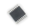
ICGOO电子元器件商城为您提供PCA9554ADB,118由NXP Semiconductors设计生产,在icgoo商城现货销售,并且可以通过原厂、代理商等渠道进行代购。 PCA9554ADB,118价格参考。NXP SemiconductorsPCA9554ADB,118封装/规格:接口 - I/O 扩展器, I/O Expander 8 I²C, SMBus 400kHz 16-SSOP。您可以下载PCA9554ADB,118参考资料、Datasheet数据手册功能说明书,资料中有PCA9554ADB,118 详细功能的应用电路图电压和使用方法及教程。
NXP USA Inc. 的 PCA9554ADB,118 是一款基于 I²C 和 SMBus 接口的 8 位 I/O 扩展器,属于接口 - I/O 扩展器类别。该器件通过两线制串行总线(I²C)与主控制器通信,有效扩展微控制器或处理器的通用输入/输出(GPIO)引脚数量。

其典型应用场景包括:

1. 工业控制:用于PLC、传感器接口和继电器控制模块中,实现对多个数字信号的监控与控制。
2. 消费电子:在家电、智能家居设备中管理LED指示灯、按键输入及开关信号。
3. 通信设备:应用于路由器、交换机等网络设备中,用于系统状态监测、电源管理和板卡识别。
4. 计算机外设:如打印机、键盘、显示器等,用于简化主控芯片的I/O负担。
5. 嵌入式系统:在MCU或MPU GPIO资源有限时,作为I/O扩展方案,支持中断输出功能,提升系统响应效率。

PCA9554ADB,118 采用 16 引脚 SO 封装,工作温度范围宽(-40°C 至 +85°C),适合工业级应用环境。其低功耗、高可靠性和简单接口设计,使其成为多种电子系统中理想的I/O扩展解决方案。
| 参数 | 数值 |
| 产品目录 | 集成电路 (IC)半导体 |
| 描述 | IC I/O EXPANDER I2C 8B 16SSOPI2C 接口集成电路 8-BIT I2C FM TP GPIO INT PU |
| 产品分类 | |
| I/O数 | 8 |
| 品牌 | NXP Semiconductors |
| 产品手册 | |
| 产品图片 |
|
| rohs | 符合RoHS无铅 / 符合限制有害物质指令(RoHS)规范要求 |
| 产品系列 | 接口 IC,I2C 接口集成电路,NXP Semiconductors PCA9554ADB,118- |
| 数据手册 | |
| 产品型号 | PCA9554ADB,118 |
| PCN封装 | |
| 中断输出 | 是 |
| 产品培训模块 | http://www.digikey.cn/PTM/IndividualPTM.page?site=cn&lang=zhs&ptm=25410http://www.digikey.cn/PTM/IndividualPTM.page?site=cn&lang=zhs&ptm=30172 |
| 产品目录页面 | |
| 产品种类 | I2C 接口集成电路 |
| 供应商器件封装 | 16-SSOP |
| 其它名称 | 568-4516-6 |
| 包装 | Digi-Reel® |
| 商标 | NXP Semiconductors |
| 安装类型 | 表面贴装 |
| 安装风格 | SMD/SMT |
| 封装 | Reel |
| 封装/外壳 | 16-SSOP(0.209",5.30mm 宽) |
| 封装/箱体 | SSOP-16 |
| 工作温度 | -40°C ~ 85°C |
| 工厂包装数量 | 2000 |
| 接口 | I²C, SMBus |
| 描述/功能 | 8-bit 12C-bus and SMBus |
| 最大工作温度 | + 85 C |
| 最大工作频率 | 400 kHz |
| 最小工作温度 | - 40 C |
| 标准包装 | 1 |
| 特性 | POR |
| 特色产品 | http://www.digikey.com/cn/zh/ph/NXP/I2C.htmlhttp://www.digikey.cn/product-highlights/cn/zh/nxp-semiconductors-agile-i-o-gpio-expander/3040 |
| 电压-电源 | 2.3 V ~ 5.5 V |
| 电流-灌/拉输出 | 10mA, 25mA |
| 电源电压-最大 | 5.5 V |
| 电源电压-最小 | 2.3 V |
| 系列 | PCA9554A |
| 输出类型 | 推挽式 |
| 配用 | /product-detail/zh/OM6278,598/568-4002-ND/1213120 |
| 零件号别名 | PCA9554ADB-T |
| 频率-时钟 | 400kHz |


- 商务部:美国ITC正式对集成电路等产品启动337调查
- 曝三星4nm工艺存在良率问题 高通将骁龙8 Gen1或转产台积电
- 太阳诱电将投资9.5亿元在常州建新厂生产MLCC 预计2023年完工
- 英特尔发布欧洲新工厂建设计划 深化IDM 2.0 战略
- 台积电先进制程称霸业界 有大客户加持明年业绩稳了
- 达到5530亿美元!SIA预计今年全球半导体销售额将创下新高
- 英特尔拟将自动驾驶子公司Mobileye上市 估值或超500亿美元
- 三星加码芯片和SET,合并消费电子和移动部门,撤换高东真等 CEO
- 三星电子宣布重大人事变动 还合并消费电子和移动部门
- 海关总署:前11个月进口集成电路产品价值2.52万亿元 增长14.8%


PDF Datasheet 数据手册内容提取
PCA9554; PCA9554A 8-bit I2C-bus and SMBus I/O port with interrupt Rev. 10 — 8 November 2017 Product data sheet 1. General description The PCA9554 and PCA9554A are 16-pin CMOS devices that provide 8bits of General Purpose parallel Input/Output (GPIO) expansion for I2C-bus/SMBus applications and were developed to enhance the NXP Semiconductors family of I2C-bus I/O expanders. The improvements include higher drive capability, 5V I/O tolerance, lower supply current, individual I/O configuration, 400kHz clock frequency, and smaller packaging. I/O expanders provide a simple solution when additional I/O is needed for ACPI power switches, sensors, pushbuttons, LEDs, fans, and so on. The PCA9554/PCA9554A consist of an 8-bit Configuration register (Input or Output selection); 8-bit Input Port register, 8-bit Output Port register and an 8-bit Polarity Inversion register (activeHIGH or activeLOW operation). The system master can enable the I/Os as either inputs or outputs by writing to the I/O configuration bits. The data for each input or output is kept in the corresponding InputPort or OutputPort register. The polarity of the read register can be inverted with the Polarity Inversion register. All registers can be read by the system master. Although pin-to-pin and I2C-bus address compatible with the PCF8574 series, software changes are required due to the enhancements and are discussed in Application Note AN469. The PCA9554/PCA9554A open-drain interrupt output is activated when any input state differs from its corresponding Input Port register state and is used to indicate to the system master that an input state has changed. The power-on reset sets the registers to their default values and initializes the device state machine. Three hardware pins (A0, A1, A2) vary the fixed I2C-bus address and allow up to eight devices to share the same I2C-bus/SMBus. The PCA9554A is identical to the PCA9554 except that the fixed I2C-bus address is different allowing up to sixteen of these devices (eight of each) on the same I2C-bus/SMBus. 2. Features and benefits Operating power supply voltage range of 2.3V to 5.5V 5V tolerant I/Os Polarity Inversion register ActiveLOW interrupt output Low standby current Noise filter on SCL/SDA inputs No glitch on power-up Internal power-on reset 8 I/O pins which default to 8 inputs 0Hz to 400kHz clock frequency
PCA9554; PCA9554A NXP Semiconductors 8-bit I2C-bus and SMBus I/O port with interrupt ESD protection exceeds 2000V HBM per JESD22-A114 and 1000V CDM per JESD22-C101 Latch-up testing is done to JEDEC Standard JESD78 which exceeds 100mA AEC-Q100 compliance available Packages offered: SO16, SSOP16, SSOP20, TSSOP16, HVQFN16(2versions: 440.85mm and 330.85mm), and bare die 3. Ordering information Table 1. Ordering info rmation Type number Topside Package marking Name Description Version PCA9554D PCA9554D SO16 plastic small outline package; 16leads; SOT162-1 bodywidth7.5mm PCA9554AD PCA9554AD PCA9554DB 9554DB SSOP16 plastic shrink small outline package; 16leads; SOT338-1 bodywidth5.3mm PCA9554ADB 9554A PCA9554TS PCA9554 SSOP20 plastic shrink small outline package; 20leads; SOT266-1 bodywidth4.4mm PCA9554ATS PA9554A PCA9554PW 9554DH TSSOP16 plastic thin shrink small outline package; 16leads; SOT403-1 bodywidth4.4mm PCA9554PW/Q900[1] 9554DH PCA9554APW 9554ADH PCA9554BS 9554 HVQFN16 plastic thermal enhanced very thin quad flat package; SOT629-1 noleads; 16terminals; body440.85mm PCA9554ABS 554A PCA9554BS3 P54 HVQFN16 plastic thermal enhanced very thin quad flat package; SOT758-1 noleads; 16terminals; body330.85mm PCA9554ABS3 54A PCA9554U - bare die - - [1] PCA9554PW/Q900 is AEC-Q100 compliant. Contact i2c.support@nxp.com for PPAP. 3.1 Ordering options Table 2. Ordering opt ions Type number Orderable Package Packing method Minimum Temperature partnumber order quantity PCA9554D PCA9554D,112 SO16 Standard marking * 1920 T =40Cto+85C amb IC’stube - DSC bulk pack PCA9554D,118 SO16 Reel 13” Q1/T1 1000 T =40Cto+85C amb *standardmark SMD PCA9554AD PCA9554AD,112 SO16 Standard marking * 1920 T =40Cto+85C amb IC’stube - DSC bulk pack PCA9554AD,118 SO16 Reel 13” Q1/T1 1000 T =40Cto+85C amb *standardmark SMD PCA9554DB PCA9554DB,112 SSOP16 Standard marking * 1092 T =40Cto+85C amb IC’stube - DSC bulk pack PCA9554DB,118 SSOP16 Reel 13” Q1/T1 2000 T =40Cto+85C amb *standardmark SMD PCA9554_9554A All information provided in this document is subject to legal disclaimers. © NXP Semiconductors N.V. 2017. All rights reserved. Product data sheet Rev. 10 — 8 November 2017 2 of 35
PCA9554; PCA9554A NXP Semiconductors 8-bit I2C-bus and SMBus I/O port with interrupt Table 2. Ordering options …continued Type number Orderable Package Packing method Minimum Temperature partnumber order quantity PCA9554ADB PCA9554ADB,112 SSOP16 Standard marking * 1092 T =40Cto+85C amb IC’stube - DSC bulk pack PCA9554ADB,118 SSOP16 Reel 13” Q1/T1 2000 T =40Cto+85C amb *standardmark SMD PCA9554TS PCA9554TS,112 SSOP20 Standard marking * 1350 T =40Cto+85C amb IC’stube - DSC bulk pack PCA9554TS,118 SSOP20 Reel 13” Q1/T1 2500 T =40Cto+85C amb *standardmark SMD PCA9554ATS PCA9554ATS,112 SSOP20 Standard marking * 1350 T =40Cto+85C amb IC’stube - DSC bulk pack PCA9554ATS,118 SSOP20 Reel 13” Q1/T1 2500 T =40Cto+85C amb *standardmark SMD PCA9554PW PCA9554PW,112 TSSOP16 Standard marking * 2400 T =40Cto+85C amb IC’stube - DSC bulk pack PCA9554PW,118 TSSOP16 Reel 13” Q1/T1 2500 T =40Cto+85C amb *standardmark SMD PCA9554PW/Q900 PCA9554PW/Q900,118 TSSOP16 Reel 13” Q1/T1 2500 T =40Cto+85C amb *standardmark SMD PCA9554APW PCA9554APW,112 TSSOP16 Standard marking * 2400 T =40Cto+85C amb IC’stube - DSC bulk pack PCA9554APW,118 TSSOP16 Reel 13” Q1/T1 2500 T =40Cto+85C amb *standardmark SMD PCA9554BS PCA9554BS,118 HVQFN16 Reel 13” Q1/T1 6000 T =40Cto+85C amb *standardmark SMD PCA9554ABS PCA9554ABS,118 HVQFN16 Reel 13” Q1/T1 6000 T =40Cto+85C amb *standardmark SMD PCA9554BS3 PCA9554BS3,118 HVQFN16 Reel 13” Q1/T1 6000 T =40Cto+85C amb *standardmark SMD PCA9554ABS3 PCA9554ABS3,118 HVQFN16 Reel 13” Q1/T1 6000 T =40Cto+85C amb *standardmark SMD PCA9554U PCA9554U,029 bare die Reel 7” Q1/T1 *no mark 7000 T =40Cto+85C amb diemounted on punched tape PCA9554_9554A All information provided in this document is subject to legal disclaimers. © NXP Semiconductors N.V. 2017. All rights reserved. Product data sheet Rev. 10 — 8 November 2017 3 of 35
PCA9554; PCA9554A NXP Semiconductors 8-bit I2C-bus and SMBus I/O port with interrupt 4. Block diagram PCA9554/PCA9554A A0 IO0 A1 IO1 A2 8-bit IO2 SSDCAL FINILPTUETR I2C-BUS/SMBus OINUPTUPUT/T IIOO43 CONTROL write pulse PORTS IO5 IO6 VDD POWER-ON read pulse IO7 RESET VDD VSS LP INT FILTER 002aac492 All I/Os are set to inputs at reset. Fig 1. Block diagram of PCA9554/PCA9554A PCA9554_9554A All information provided in this document is subject to legal disclaimers. © NXP Semiconductors N.V. 2017. All rights reserved. Product data sheet Rev. 10 — 8 November 2017 4 of 35
PCA9554; PCA9554A NXP Semiconductors 8-bit I2C-bus and SMBus I/O port with interrupt 5. Pinning information 5.1 Pinning A0 1 16 VDD A0 1 16 VDD A1 2 15 SDA A1 2 15 SDA A2 3 14 SCL A2 3 14 SCL IO0 4 PCA9554DB 13 INT IO0 4 PCA9554D 13 INT IO1 5 PCA9554AD 12 IO7 IO1 5 PCA9554ADB 12 IO7 IO2 6 11 IO6 IO2 6 11 IO6 IO3 7 10 IO5 IO3 7 10 IO5 VSS 8 9 IO4 VSS 8 9 IO4 002aac486 002aac487 Fig 2. Pin configuration for SO16 Fig 3. Pin configuration for SSOP16 INT 1 20 IO7 SCL 2 19 IO6 A0 1 16 VDD n.c. 3 18 n.c. A1 2 15 SDA SDA 4 17 IO5 A2 3 14 SCL VDD 5 PCA9554TS 16 IO4 IO0 4 PCA9554PW 13 INT A0 6 PCA9554ATS 15 VSS PCA9554PW/Q900 IO1 5 12 IO7 A1 7 14 IO3 PCA9554APW IO2 6 11 IO6 n.c. 8 13 n.c. IO3 7 10 IO5 A2 9 12 IO2 VSS 8 9 IO4 IO0 10 11 IO1 002aac488 002aac489 Fig 4. Pin configuration for TSSOP16 Fig 5. Pin configuration for SSOP20 PCA9554BS PCA9554BS3 PCA9554ABS PCA9554ABS3 D A D A terminal 1 1 0 D D terminal 1 1 0 D D A A V S A A V S index area index area 6 5 4 3 6 5 4 3 1 1 1 1 1 1 1 1 A2 1 12 SCL A2 1 12 SCL IO0 2 11 INT IO0 2 11 INT IO1 3 10 IO7 IO1 3 10 IO7 IO2 4 9 IO6 IO2 4 9 IO6 5 6 7 8 5 6 7 8 3 S 4 5 3 S 4 5 IO VS IO IO 002aac490 IO VS IO IO 002aac491 Transparent top view Transparent top view Fig 6. Pin configuration for HVQFN16 Fig 7. Pin configuration for HVQFN16 (SOT629-1) (SOT758-1) PCA9554_9554A All information provided in this document is subject to legal disclaimers. © NXP Semiconductors N.V. 2017. All rights reserved. Product data sheet Rev. 10 — 8 November 2017 5 of 35
PCA9554; PCA9554A NXP Semiconductors 8-bit I2C-bus and SMBus I/O port with interrupt 5.2 Pin description Table 3. Pin description Symbol Pin Description SO16, SSOP16, HVQFN16 SSOP20 TSSOP16 A0 1 15 6 address input 0 A1 2 16 7 address input 1 A2 3 1 9 address input 2 IO0 4 2 10 input/output 0 IO1 5 3 11 input/output 1 IO2 6 4 12 input/output 2 IO3 7 5 14 input/output 3 V 8 6[1] 15 supply ground SS IO4 9 7 16 input/output 4 IO5 10 8 17 input/output 5 IO6 11 9 19 input/output 6 IO7 12 10 20 input/output 7 INT 13 11 1 interrupt output (open-drain) SCL 14 12 2 serial clock line SDA 15 13 4 serial data line V 16 14 5 supply voltage DD n.c. - - 3, 8, 13, 18 not connected [1] HVQFN16 package die supply ground is connected to both V pin and exposed center pad. V pin must SS SS be connected to supply ground for proper device operation. For enhanced thermal, electrical, and board level performance, the exposed pad needs to be soldered to the board using a corresponding thermal pad on the board and for proper heat conduction through the board, thermal vias need to be incorporated in the PCB in the thermal pad region. 6. Functional description Refer to Figure 1 “Block diagram of PCA9554/PCA9554A”. 6.1 Registers 6.1.1 Command byte Table 4. Command byte Command Protocol Function 0 read byte Input Port register 1 read/write byte Output Port register 2 read/write byte Polarity Inversion register 3 read/write byte Configuration register The command byte is the first byte to follow the address byte during a write transmission. It is used as a pointer to determine which of the following registers will be written or read. PCA9554_9554A All information provided in this document is subject to legal disclaimers. © NXP Semiconductors N.V. 2017. All rights reserved. Product data sheet Rev. 10 — 8 November 2017 6 of 35
PCA9554; PCA9554A NXP Semiconductors 8-bit I2C-bus and SMBus I/O port with interrupt 6.1.2 Register 0 - Input Port register This register is a read-only port. It reflects the incoming logic levels of the pins, regardless of whether the pin is defined as an input or an output by Register 3. Writes to this register have no effect. The default ‘X’ is determined by the externally applied logic level, normally ‘1’ when no external signal externally applied because of the internal pull-up resistors. Table 5. Register 0 - Input Port register bit description Bit Symbol Access Value Description 7 I7 read only X determined by externally applied logic level 6 I6 read only X 5 I5 read only X 4 I4 read only X 3 I3 read only X 2 I2 read only X 1 I1 read only X 0 I0 read only X 6.1.3 Register 1 - Output Port register This register reflects the outgoing logic levels of the pins defined as outputs by Register 3. Bit values in this register have no effect on pins defined as inputs. Reads from this register return the value that is in the flip-flop controlling the output selection, not the actual pin value. Table 6. Register 1 - Output Port register bit description Legend: * default value. Bit Symbol Access Value Description 7 O7 R 1* reflects outgoing logic levels of pins defined as outputs by Register 3 6 O6 R 1* 5 O5 R 1* 4 O4 R 1* 3 O3 R 1* 2 O2 R 1* 1 O1 R 1* 0 O0 R 1* PCA9554_9554A All information provided in this document is subject to legal disclaimers. © NXP Semiconductors N.V. 2017. All rights reserved. Product data sheet Rev. 10 — 8 November 2017 7 of 35
PCA9554; PCA9554A NXP Semiconductors 8-bit I2C-bus and SMBus I/O port with interrupt 6.1.4 Register 2 - Polarity Inversion register This register allows the user to invert the polarity of the Input Port register data. If a bit in this register is set (written with ‘1’), the corresponding Input Port data is inverted. If a bit in this register is cleared (written with a ‘0’), the Input Port data polarity is retained. Table 7. Register 2 - Polarity Inversion register bit description Legend: * default value. Bit Symbol Access Value Description 7 N7 R/W 0* inverts polarity of Input Port register data 6 N6 R/W 0* 0 = Input Port register data retained (default value) 5 N5 R/W 0* 1 = Input Port register data inverted 4 N4 R/W 0* 3 N3 R/W 0* 2 N2 R/W 0* 1 N1 R/W 0* 0 N0 R/W 0* 6.1.5 Register 3 - Configuration register This register configures the directions of the I/O pins. If a bit in this register is set, the corresponding port pin is enabled as an input with high-impedance output driver. If a bit in this register is cleared, the corresponding port pin is enabled as an output. At reset, the I/Os are configured as inputs with a weak pull-up to V . DD Table 8. Register 3 - Configuration register bit description Legend: * default value. Bit Symbol Access Value Description 7 C7 R/W 1* configures the directions of the I/O pins 6 C6 R/W 1* 0 = corresponding port pin enabled as an output 5 C5 R/W 1* 1 = corresponding port pin configured as input (default value) 4 C4 R/W 1* 3 C3 R/W 1* 2 C2 R/W 1* 1 C1 R/W 1* 0 C0 R/W 1* 6.2 Power-on reset When power is applied to V , an internal Power-On Reset (POR) holds the DD PCA9554/PCA9554A in a reset condition until V has reached V . At that point, the DD POR reset condition is released and the PCA9554/PCA9554A registers and state machine will initialize to their default states. Thereafter, V must be lowered below 0.2V to reset the DD device. For a power reset cycle, V must be lowered below 0.2V and then restored to the DD operating voltage. PCA9554_9554A All information provided in this document is subject to legal disclaimers. © NXP Semiconductors N.V. 2017. All rights reserved. Product data sheet Rev. 10 — 8 November 2017 8 of 35
PCA9554; PCA9554A NXP Semiconductors 8-bit I2C-bus and SMBus I/O port with interrupt 6.3 Interrupt output The open-drain interrupt output is activated when one of the port pins change state and the pin is configured as an input. The interrupt is deactivated when the input returns to its previous state or the Input Port register is read. Note that changing an I/O from and output to an input may cause a false interrupt to occur if the state of the pin does not match the contents of the Input Port register. 6.4 I/O port When an I/O is configured as an input, FETs Q1 and Q2 are off, creating a high-impedance input with a weak pull-up (100k typ.) to V . The input voltage may be DD raised above V to a maximum of 5.5V. DD If the I/O is configured as an output, then either Q1 or Q2 is enabled, depending on the state of the Output Port register. Care should be exercised if an external voltage is applied to an I/O configured as an output because of the low-impedance paths that exist between the pin and either V or V . DD SS data from shift register output port register data configuration register VDD data from D Q Q1 shift register FF 100 kΩ write configuration D Q pulse CK Q FF IO0 to IO7 write pulse CK Q2 output port register VSS input port register D Q input port FF register data read pulse CK to INT polarity inversion register data from D Q polarity inversion shift register register data FF write polarity pulse CK 002aac493 Remark: At power-on reset, all registers return to default values. Fig 8. Simplified schematic of IO0 to IO7 PCA9554_9554A All information provided in this document is subject to legal disclaimers. © NXP Semiconductors N.V. 2017. All rights reserved. Product data sheet Rev. 10 — 8 November 2017 9 of 35
PCA9554; PCA9554A NXP Semiconductors 8-bit I2C-bus and SMBus I/O port with interrupt 6.5 Device address slave address slave address 0 1 0 0 A2 A1 A0 R/W 0 1 1 1 A2 A1 A0 R/W fixed hardware fixed hardware selectable selectable 002aac494 002aac495 Fig 9. PCA9554 device address Fig 10. PCA9554A device address 6.6 Bus transactions Data is transmitted to the PCA9554/PCA9554A registers using the Write mode as shown in Figure11 and Figure12. Data is read from the PCA9554/PCA9554A registers using the Read mode as shown in Figure13 and Figure14. These devices do not implement an auto-increment function, so once a command byte has been sent, the register which was addressed will continue to be accessed by reads until a new command byte has been sent. SCL 1 2 3 4 5 6 7 8 9 slave address command byte data to port SDA S 0 1 0 0 A2 A1 A0 0 A 0 0 0 0 0 0 0 1 A DATA 1 A P START condition R/W acknowledge acknowledge STOP from slave from slave condition acknowledge from slave write to port tv(Q) data out data 1 valid from port 002aac472 Fig 11. Write to Output Port register SCL 1 2 3 4 5 6 7 8 9 slave address command byte data to register SDA S 0 1 0 0 A2 A1 A0 0 A 0 0 0 0 0 0 1 1/0 A DATA A P START condition R/W acknowledge acknowledge STOP from slave from slave condition acknowledge from slave data to register 002aac473 Fig 12. Write to Configuration register or Polarity Inversion register PCA9554_9554A All information provided in this document is subject to legal disclaimers. © NXP Semiconductors N.V. 2017. All rights reserved. Product data sheet Rev. 10 — 8 November 2017 10 of 35
PCA9554; PCA9554A NXP Semiconductors 8-bit I2C-bus and SMBus I/O port with interrupt slave address SDA S 0 1 0 0 A2 A1 A0 0 A command byte A (cont.) START condition R/W acknowledge from slave acknowledge from slave slave address data from register data from register (cont.) S 0 1 0 0 A2 A1 A0 1 A DATA (first byte) A DATA (last byte) NA P (repeated) R/W acknowledge no acknowledge STOP START condition from master from master condition acknowledge from slave at this moment master-transmitter becomes master-receiver and slave-receiver becomes slave-transmitter 002aac474 Fig 13. Read from register SCL 1 2 3 4 5 6 7 8 9 slave address data from port data from port SDA S 0 1 0 0 A2 A1 A0 1 A DATA 1 A DATA 4 NA P START condition R/W acknowledge no acknowledge STOP from master from master condition acknowledge from slave read from port th(D) tsu(D) data into port DATA 2 DATA 3 DATA 4 tv(INT_N) trst(INT_N) INT 002aac475 This figure assumes the command byte has previously been programmed with 00h. Transfer of data can be stopped at any moment by a STOP condition. Fig 14. Read Input Port register PCA9554_9554A All information provided in this document is subject to legal disclaimers. © NXP Semiconductors N.V. 2017. All rights reserved. Product data sheet Rev. 10 — 8 November 2017 11 of 35
PCA9554; PCA9554A NXP Semiconductors 8-bit I2C-bus and SMBus I/O port with interrupt 7. Application design-in information VDD (5 V) 10 kΩ 10 kΩ 10 kΩ 10 kΩ 2 kΩ VDD VDD MASTER PCA9554 CONTROLLER SUBSYSTEM 1 SCL SCL IO0 (e.g., temp. sensor) SDA SDA IO1 INT IO2 RESET INT INT IO3 SUBSYSTEM 2 IO4 (e.g., counter) VSS IO5 IO6 A IO7 enable controlled switch A2 (e.g., CBT device) A1 A0 B VSS ALARM SUBSYSTEM 3 (e.g., alarm system) VDD 002aac496 Device address configured as 0100100X for this example. IO0, IO1, IO2 configured as outputs. IO3, IO4, IO5 configured as inputs. IO6 and IO7 are not used and must be configured as outputs. Fig 15. Typical application 8. Limiting values Table 9. Limiting values In accordance with the Absolute Maximum Rating System (IEC 60134). Symbol Parameter Conditions Min Max Unit V supply voltage 0.5 +6.0 V DD I input current - 20 mA I V voltage on an input/output pin V 0.5 5.5 V I/O SS I output current on pin IOn - 50 mA O(IOn) I supply current - 85 mA DD I ground supply current - 100 mA SS P total power dissipation - 200 mW tot T storage temperature 65 +150 C stg T ambient temperature operating 40 +85 C amb PCA9554_9554A All information provided in this document is subject to legal disclaimers. © NXP Semiconductors N.V. 2017. All rights reserved. Product data sheet Rev. 10 — 8 November 2017 12 of 35
PCA9554; PCA9554A NXP Semiconductors 8-bit I2C-bus and SMBus I/O port with interrupt 9. Static characteristics Table 10. Static charac teristics V =2.3V to 5.5V; V =0V; T =40C to +85C; unless otherwise specified. DD SS amb Symbol Parameter Conditions Min Typ Max Unit Supplies V supply voltage 2.3 - 5.5 V DD I supply current operating mode; V =5.5V; - 104 175 A DD DD noload; f =100kHz SCL I standby current Standby mode; V =5.5V; noload; - 550 700 A stb DD V =V ; f =0kHz; I/O=inputs I SS SCL Standby mode; V =5.5V; noload; - 0.25 1 A DD V =V ; f =0kHz; I/O=inputs I DD SCL V power-on reset voltage no load; V =V or V [1] - 1.7 2.2 V POR I DD SS Input SCL; input/output SDA V LOW-level input voltage 0.5 - +0.3V V IL DD V HIGH-level input voltage 0.7V - 5.5 V IH DD I LOW-level output current V =0.4V 3 6 - mA OL OL I leakage current V =V =V 1 - +1 A L I DD SS C input capacitance V =V - 6 10 pF i I SS I/Os V LOW-level input voltage 0.5 - +0.8 V IL V HIGH-level input voltage 2.0 - 5.5 V IH I LOW-level output current V =0.5V; V =2.3V [2] 8 10 - mA OL OL DD V =0.7V; V =2.3V [2] 10 13 - mA OL DD V =0.5V; V =3.0V [2] 8 14 - mA OL DD V =0.7V; V =3.0V [2] 10 19 - mA OL DD V =0.5V; V =4.5V [2] 8 17 - mA OL DD V =0.7V; V =4.5V [2] 10 24 - mA OL DD V HIGH-level output voltage I =8mA; V =2.3V [3] 1.8 - - V OH OH DD I =10mA; V =2.3V [3] 1.7 - - V OH DD I =8mA; V =3.0V [3] 2.6 - - V OH DD I =10mA; V =3.0V [3] 2.5 - - V OH DD I =8mA; V =4.75V [3] 4.1 - - V OH DD I =10mA; V =4.75V [3] 4.0 - - V OH DD I input leakage current V =3.6V; V =V 1 - +1 A LI DD I DD I leakage current V =5.5V; V =V - - 100 A L DD I SS C input capacitance - 3.7 5 pF i C output capacitance - 3.7 5 pF o Interrupt INT I LOW-level output current V =0.4V 3 - - mA OL OL PCA9554_9554A All information provided in this document is subject to legal disclaimers. © NXP Semiconductors N.V. 2017. All rights reserved. Product data sheet Rev. 10 — 8 November 2017 13 of 35
PCA9554; PCA9554A NXP Semiconductors 8-bit I2C-bus and SMBus I/O port with interrupt Table 10. Static characteristics …continued V =2.3V to 5.5V; V =0V; T =40C to +85C; unless otherwise specified. DD SS amb Symbol Parameter Conditions Min Typ Max Unit Select inputs A0, A1, A2 V LOW-level input voltage 0.5 - 0.8 V IL V HIGH-level input voltage 2.0 - 5.5 V IH I input leakage current 1 - 1 A LI [1] VDD must be lowered to 0.2V for at least 5s in order to reset part. [2] Each I/O must be externally limited to a maximum of 25mA and the device must be limited to a maximum current of 100mA. [3] The total current sourced by all I/Os must be limited to 85mA. 10. Dynamic characteristics Table 11. Dynamic cha racteristics Symbol Parameter Conditions Standard-mode Fast-mode I2C-bus Unit I2C-bus Min Max Min Max f SCL clock frequency 0 100 0 400 kHz SCL t bus free time between a STOP and 4.7 - 1.3 - s BUF START condition t hold time (repeated) START condition 4.0 - 0.6 - s HD;STA t set-up time for a repeated START 4.7 - 0.6 - s SU;STA condition t set-up time for STOP condition 4.0 - 0.6 - s SU;STO t data hold time 0 - 0 - s HD;DAT t data valid acknowledge time [1] 0.3 3.45 0.1 0.9 s VD;ACK t data valid time [2] 300 - 50 - ns VD;DAT t data set-up time 250 - 100 - ns SU;DAT t LOW period of the SCL clock 4.7 - 1.3 - s LOW t HIGH period of the SCL clock 4.0 - 0.6 - s HIGH t rise time of both SDA and SCL signals - 1000 20+0.1C [3] 300 ns r b t fall time of both SDA and SCL signals - 300 20+0.1C [3] 300 ns f b t pulse width of spikes that must be - 50 - 50 ns SP suppressed by the input filter Port timing t data output valid time - 200 - 200 ns v(Q) t data input set-up time 100 - 100 - ns su(D) t data input hold time 1 - 1 - s h(D) Interrupt timing t valid time on pin INT - 4 - 4 s v(INT_N) t reset time on pin INT - 4 - 4 s rst(INT_N) [1] t = time for Acknowledgement signal from SCL LOW to SDA (out) LOW. VD;ACK [2] t = minimum time for SDA data output to be valid following SCL LOW. VD;DAT [3] C =total capacitance of one bus line in pF. b PCA9554_9554A All information provided in this document is subject to legal disclaimers. © NXP Semiconductors N.V. 2017. All rights reserved. Product data sheet Rev. 10 — 8 November 2017 14 of 35
PCA9554; PCA9554A NXP Semiconductors 8-bit I2C-bus and SMBus I/O port with interrupt 0.7 × VDD SDA 0.3 × VDD tBUF tr tf tHD;STA tSP tLOW 0.7 × VDD SCL 0.3 × VDD tHD;STA tSU;STA tSU;STO P S tHD;DAT tHIGH tSU;DAT Sr P 002aaa986 Fig 16. Definition of timing PCA9554_9554A All information provided in this document is subject to legal disclaimers. © NXP Semiconductors N.V. 2017. All rights reserved. Product data sheet Rev. 10 — 8 November 2017 15 of 35
PCA9554; PCA9554A NXP Semiconductors 8-bit I2C-bus and SMBus I/O port with interrupt 11. Package outline SO16: plastic small outline package; 16 leads; body width 7.5 mm SOT162-1 D E A X c y HE v M A Z 16 9 Q A2 A A1 (A 3 ) pin 1 index θ Lp L 1 8 detail X e w M bp 0 5 10 mm scale DIMENSIONS (inch dimensions are derived from the original mm dimensions) UNIT mAax. A1 A2 A3 bp c D(1) E(1) e HE L Lp Q v w y Z(1) θ 0.3 2.45 0.49 0.32 10.5 7.6 10.65 1.1 1.1 0.9 mm 2.65 0.25 1.27 1.4 0.25 0.25 0.1 0.1 2.25 0.36 0.23 10.1 7.4 10.00 0.4 1.0 0.4 8o 0.012 0.096 0.019 0.013 0.41 0.30 0.419 0.043 0.043 0.035 0o inches 0.1 0.01 0.05 0.055 0.01 0.01 0.004 0.004 0.089 0.014 0.009 0.40 0.29 0.394 0.016 0.039 0.016 Note 1. Plastic or metal protrusions of 0.15 mm (0.006 inch) maximum per side are not included. OUTLINE REFERENCES EUROPEAN ISSUE DATE VERSION IEC JEDEC JEITA PROJECTION 99-12-27 SOT162-1 075E03 MS-013 03-02-19 Fig 17. Package outline SOT162-1 (SO16) PCA9554_9554A All information provided in this document is subject to legal disclaimers. © NXP Semiconductors N.V. 2017. All rights reserved. Product data sheet Rev. 10 — 8 November 2017 16 of 35
PCA9554; PCA9554A NXP Semiconductors 8-bit I2C-bus and SMBus I/O port with interrupt SSOP16: plastic shrink small outline package; 16 leads; body width 5.3 mm SOT338-1 D E A X c y HE v M A Z 16 9 Q A2 A1 (A 3 ) A pin 1 index θ Lp L 1 8 detail X w M e bp 0 2.5 5 mm scale DIMENSIONS (mm are the original dimensions) UNIT mAax. A1 A2 A3 bp c D(1) E(1) e HE L Lp Q v w y Z(1) θ mm 2 00..2015 11..8605 0.25 00..3285 00..2009 66..40 55..42 0.65 77..96 1.25 10..0633 00..97 0.2 0.13 0.1 10..0505 80oo Note 1. Plastic or metal protrusions of 0.25 mm maximum per side are not included. OUTLINE REFERENCES EUROPEAN ISSUE DATE VERSION IEC JEDEC JEITA PROJECTION 99-12-27 SOT338-1 MO-150 03-02-19 Fig 18. Package outline SOT338-1 (SSOP16) PCA9554_9554A All information provided in this document is subject to legal disclaimers. © NXP Semiconductors N.V. 2017. All rights reserved. Product data sheet Rev. 10 — 8 November 2017 17 of 35
PCA9554; PCA9554A NXP Semiconductors 8-bit I2C-bus and SMBus I/O port with interrupt SSOP20: plastic shrink small outline package; 20 leads; body width 4.4 mm SOT266-1 D E A X c y HE v M A Z 20 11 Q pin 1 index A2 A1 (A 3 ) A θ Lp L 1 10 detail X w M e bp 0 2.5 5 mm scale DIMENSIONS (mm are the original dimensions) UNIT mAax. A1 A2 A3 bp c D(1) E(1) e HE L Lp Q v w y Z(1) θ mm 1.5 0.015 11..42 0.25 00..3220 00..2103 66..64 44..53 0.65 66..62 1 00..7455 00..6455 0.2 0.13 0.1 00..4188 100oo Note 1. Plastic or metal protrusions of 0.20 mm maximum per side are not included. OUTLINE REFERENCES EUROPEAN ISSUE DATE VERSION IEC JEDEC JEITA PROJECTION 99-12-27 SOT266-1 MO-152 03-02-19 Fig 19. Package outline SOT266-1 (SSOP20) PCA9554_9554A All information provided in this document is subject to legal disclaimers. © NXP Semiconductors N.V. 2017. All rights reserved. Product data sheet Rev. 10 — 8 November 2017 18 of 35
PCA9554; PCA9554A NXP Semiconductors 8-bit I2C-bus and SMBus I/O port with interrupt TSSOP16: plastic thin shrink small outline package; 16 leads; body width 4.4 mm SOT403-1 D E A X c y HE v M A Z 16 9 Q A2 (A 3 ) A pin 1 index A1 θ Lp L 1 8 detail X w M e bp 0 2.5 5 mm scale DIMENSIONS (mm are the original dimensions) UNIT mAax. A1 A2 A3 bp c D(1) E(2) e HE L Lp Q v w y Z(1) θ mm 1.1 00..1055 00..9850 0.25 00..3109 00..21 54..19 44..53 0.65 66..62 1 00..7550 00..43 0.2 0.13 0.1 00..4006 80oo Notes 1. Plastic or metal protrusions of 0.15 mm maximum per side are not included. 2. Plastic interlead protrusions of 0.25 mm maximum per side are not included. OUTLINE REFERENCES EUROPEAN ISSUE DATE VERSION IEC JEDEC JEITA PROJECTION 99-12-27 SOT403-1 MO-153 03-02-18 Fig 20. Package outline SOT403-1 (TSSOP16) PCA9554_9554A All information provided in this document is subject to legal disclaimers. © NXP Semiconductors N.V. 2017. All rights reserved. Product data sheet Rev. 10 — 8 November 2017 19 of 35
PCA9554; PCA9554A NXP Semiconductors 8-bit I2C-bus and SMBus I/O port with interrupt HVQFN16: plastic thermal enhanced very thin quad flat package; no leads; 16 terminals; body 4 x 4 x 0.85 mm SOT629-1 D B A terminal 1 index area A A1 E c detail X e1 C 1/2 e e b v M C A B y1 C y 5 8 w M C L 9 4 e Eh e2 1/2 e 1 12 terminal 1 index area 16 13 Dh X 0 2.5 5 mm scale DIMENSIONS (mm are the original dimensions) A(1) UNIT max. A1 b c D(1) Dh E(1) Eh e e1 e2 L v w y y1 0.05 0.38 4.1 2.25 4.1 2.25 0.75 mm 1 0.2 0.65 1.95 1.95 0.1 0.05 0.05 0.1 0.00 0.23 3.9 1.95 3.9 1.95 0.50 Note 1. Plastic or metal protrusions of 0.075 mm maximum per side are not included. OUTLINE REFERENCES EUROPEAN ISSUE DATE VERSION IEC JEDEC JEITA PROJECTION 01-08-08 SOT629-1 - - - MO-220 - - - 02-10-22 Fig 21. Package outline SOT629-1 (HVQFN16) PCA9554_9554A All information provided in this document is subject to legal disclaimers. © NXP Semiconductors N.V. 2017. All rights reserved. Product data sheet Rev. 10 — 8 November 2017 20 of 35
PCA9554; PCA9554A NXP Semiconductors 8-bit I2C-bus and SMBus I/O port with interrupt HVQFN16: plastic thermal enhanced very thin quad flat package; no leads; 16 terminals; body 3 x 3 x 0.85 mm SOT758-1 D B A terminal 1 index area E A A1 c detail X e1 C 1/2 e v M C A B y1 C y e b w M C 5 8 L 4 9 e Eh e2 1/2 e 1 12 terminal 1 16 13 index area Dh X 0 2.5 5 mm scale DIMENSIONS (mm are the original dimensions) UNIT mAa(1x). A1 b c D(1) Dh E(1) Eh e e1 e2 L v w y y1 0.05 0.30 3.1 1.75 3.1 1.75 0.5 mm 1 0.2 0.5 1.5 1.5 0.1 0.05 0.05 0.1 0.00 0.18 2.9 1.45 2.9 1.45 0.3 Note 1. Plastic or metal protrusions of 0.075 mm maximum per side are not included. OUTLINE REFERENCES EUROPEAN ISSUE DATE VERSION IEC JEDEC JEITA PROJECTION 02-03-25 SOT758-1 - - - MO-220 - - - 02-10-21 Fig 22. Package outline SOT758-1 (HVQFN16) PCA9554_9554A All information provided in this document is subject to legal disclaimers. © NXP Semiconductors N.V. 2017. All rights reserved. Product data sheet Rev. 10 — 8 November 2017 21 of 35
PCA9554; PCA9554A NXP Semiconductors 8-bit I2C-bus and SMBus I/O port with interrupt 12. Handling information All input and output pins are protected against ElectroStatic Discharge (ESD) under normal handling. When handling ensure that the appropriate precautions are taken as described in JESD625-A or equivalent standards. 13. Soldering of SMD packages This text provides a very brief insight into a complex technology. A more in-depth account of soldering ICs can be found in Application Note AN10365 “Surface mount reflow soldering description”. 13.1 Introduction to soldering Soldering is one of the most common methods through which packages are attached to Printed Circuit Boards (PCBs), to form electrical circuits. The soldered joint provides both the mechanical and the electrical connection. There is no single soldering method that is ideal for all IC packages. Wave soldering is often preferred when through-hole and Surface Mount Devices (SMDs) are mixed on one printed wiring board; however, it is not suitable for fine pitch SMDs. Reflow soldering is ideal for the small pitches and high densities that come with increased miniaturization. 13.2 Wave and reflow soldering Wave soldering is a joining technology in which the joints are made by solder coming from a standing wave of liquid solder. The wave soldering process is suitable for the following: • Through-hole components • Leaded or leadless SMDs, which are glued to the surface of the printed circuit board Not all SMDs can be wave soldered. Packages with solder balls, and some leadless packages which have solder lands underneath the body, cannot be wave soldered. Also, leaded SMDs with leads having a pitch smaller than ~0.6mm cannot be wave soldered, due to an increased probability of bridging. The reflow soldering process involves applying solder paste to a board, followed by component placement and exposure to a temperature profile. Leaded packages, packages with solder balls, and leadless packages are all reflow solderable. Key characteristics in both wave and reflow soldering are: • Board specifications, including the board finish, solder masks and vias • Package footprints, including solder thieves and orientation • The moisture sensitivity level of the packages • Package placement • Inspection and repair • Lead-free soldering versus SnPb soldering 13.3 Wave soldering Key characteristics in wave soldering are: PCA9554_9554A All information provided in this document is subject to legal disclaimers. © NXP Semiconductors N.V. 2017. All rights reserved. Product data sheet Rev. 10 — 8 November 2017 22 of 35
PCA9554; PCA9554A NXP Semiconductors 8-bit I2C-bus and SMBus I/O port with interrupt • Process issues, such as application of adhesive and flux, clinching of leads, board transport, the solder wave parameters, and the time during which components are exposed to the wave • Solder bath specifications, including temperature and impurities 13.4 Reflow soldering Key characteristics in reflow soldering are: • Lead-free versus SnPb soldering; note that a lead-free reflow process usually leads to higher minimum peak temperatures (see Figure23) than a SnPb process, thus reducing the process window • Solder paste printing issues including smearing, release, and adjusting the process window for a mix of large and small components on one board • Reflow temperature profile; this profile includes preheat, reflow (in which the board is heated to the peak temperature) and cooling down. It is imperative that the peak temperature is high enough for the solder to make reliable solder joints (a solder paste characteristic). In addition, the peak temperature must be low enough that the packages and/or boards are not damaged. The peak temperature of the package depends on package thickness and volume and is classified in accordance with Table12 and13 Table 12. SnPb eutectic process (from J-STD-020C) Package thickness (mm) Package reflow temperature (C) Volume (mm3) < 350 350 < 2.5 235 220 2.5 220 220 Table 13. Lead-free process (from J-STD-020C) Package thickness (mm) Package reflow temperature (C) Volume (mm3) < 350 350 to 2000 > 2000 < 1.6 260 260 260 1.6 to 2.5 260 250 245 > 2.5 250 245 245 Moisture sensitivity precautions, as indicated on the packing, must be respected at all times. Studies have shown that small packages reach higher temperatures during reflow soldering, see Figure23. PCA9554_9554A All information provided in this document is subject to legal disclaimers. © NXP Semiconductors N.V. 2017. All rights reserved. Product data sheet Rev. 10 — 8 November 2017 23 of 35
PCA9554; PCA9554A NXP Semiconductors 8-bit I2C-bus and SMBus I/O port with interrupt maximum peak temperature = MSL limit, damage level temperature minimum peak temperature = minimum soldering temperature peak temperature time 001aac844 MSL: Moisture Sensitivity Level Fig 23. Temperature profiles for large and small components For further information on temperature profiles, refer to Application Note AN10365 “Surface mount reflow soldering description”. PCA9554_9554A All information provided in this document is subject to legal disclaimers. © NXP Semiconductors N.V. 2017. All rights reserved. Product data sheet Rev. 10 — 8 November 2017 24 of 35
PCA9554; PCA9554A NXP Semiconductors 8-bit I2C-bus and SMBus I/O port with interrupt 14. Soldering: PCB footprints Footprint information for reflow soldering of SO16 package SOT162-1 Hx Gx P2 (0.125) (0.125) Hy Gy By Ay C D2 (4x) P1 D1 Generic footprint pattern Refer to the package outline drawing for actual layout solder land occupied area DIMENSIONS in mm P1 P2 Ay By C D1 D2 Gx Gy Hx Hy 1.270 1.320 11.200 6.400 2.400 0.700 0.800 10.040 8.600 11.900 11.450 sot162-1_fr Fig 24. PCB footprint for SOT162-1 (SO16); reflow soldering PCA9554_9554A All information provided in this document is subject to legal disclaimers. © NXP Semiconductors N.V. 2017. All rights reserved. Product data sheet Rev. 10 — 8 November 2017 25 of 35
PCA9554; PCA9554A NXP Semiconductors 8-bit I2C-bus and SMBus I/O port with interrupt Footprint information for reflow soldering of SSOP16 package SOT338-1 Hx Gx P2 (0.125) (0.125) Hy Gy By Ay C D2 (4x) P1 D1 Generic footprint pattern Refer to the package outline drawing for actual layout solder land occupied area DIMENSIONS in mm P1 P2 Ay By C D1 D2 Gx Gy Hx Hy 0.65 0.75 8.6 5.4 1.6 0.4 0.6 5.6 6.1 7.0 8.85 Issue date 09-02-22 sot338-1_fr 15-03-26 Fig 25. PCB footprint for SOT338-1 (HVQFN16); reflow soldering PCA9554_9554A All information provided in this document is subject to legal disclaimers. © NXP Semiconductors N.V. 2017. All rights reserved. Product data sheet Rev. 10 — 8 November 2017 26 of 35
PCA9554; PCA9554A NXP Semiconductors 8-bit I2C-bus and SMBus I/O port with interrupt Footprint information for reflow soldering of SSOP20 package SOT266-1 Hx Gx P2 (0.125) (0.125) Hy Gy By Ay C D2 (4x) P1 D1 Generic footprint pattern Refer to the package outline drawing for actual layout solder land occupied area DIMENSIONS in mm P1 P2 Ay By C D1 D2 Gx Gy Hx Hy 0.650 0.750 7.200 4.500 1.350 0.400 0.600 6.900 5.300 7.300 7.450 sot266-1_fr Fig 26. PCB footprint for SOT266-1 (SSOP20); reflow soldering PCA9554_9554A All information provided in this document is subject to legal disclaimers. © NXP Semiconductors N.V. 2017. All rights reserved. Product data sheet Rev. 10 — 8 November 2017 27 of 35
PCA9554; PCA9554A NXP Semiconductors 8-bit I2C-bus and SMBus I/O port with interrupt Footprint information for reflow soldering of TSSOP16 package SOT403-1 Hx Gx P2 (0.125) (0.125) Hy Gy By Ay C D2 (4x) P1 D1 Generic footprint pattern Refer to the package outline drawing for actual layout solder land occupied area DIMENSIONS in mm P1 P2 Ay By C D1 D2 Gx Gy Hx Hy 0.650 0.750 7.200 4.500 1.350 0.400 0.600 5.600 5.300 5.800 7.450 sot403-1_fr Fig 27. PCB footprint for SOT403-1 (TSSOP16); reflow soldering PCA9554_9554A All information provided in this document is subject to legal disclaimers. © NXP Semiconductors N.V. 2017. All rights reserved. Product data sheet Rev. 10 — 8 November 2017 28 of 35
PCA9554; PCA9554A NXP Semiconductors 8-bit I2C-bus and SMBus I/O port with interrupt Footprint information for reflow soldering of HVQFN16 package SOT629-1 Hx Gx D P 0.025 0.025 C (0.105) SPx nSPx SPy ot Hy Gy y t SLy By Ay P nSPy S SPx tot SLx Bx Ax Generic footprint pattern Refer to the package outline drawing for actual layout solder land solder paste deposit solder land plus solder paste occupied area nSPx nSPy 2 2 Dimensions in mm P Ax Ay Bx By C D SLx SLy SPx tot SPy tot SPx SPy Gx Gy Hx Hy 0.650 5.000 5.000 2.800 2.800 1.100 0.300 2.000 2.000 1.200 1.200 0.450 0.450 4.300 4.300 5.250 5.250 07-05-07 Issue date sot629-1_fr 09-06-15 Fig 28. PCB footprint for SOT629-1 (HVQFN16); reflow soldering PCA9554_9554A All information provided in this document is subject to legal disclaimers. © NXP Semiconductors N.V. 2017. All rights reserved. Product data sheet Rev. 10 — 8 November 2017 29 of 35
PCA9554; PCA9554A NXP Semiconductors 8-bit I2C-bus and SMBus I/O port with interrupt Footprint information for reflow soldering of HVQFN16 package SOT758-1 Hx Gx D P 0.025 0.025 C (0.105) SPx nSPx SPy ot Hy Gy y t nSPy SLy By Ay P S SPx tot SLx Bx Ax solder land solder paste deposit solder land plus solder paste occupied area nSPx nSPy 2 2 Dimensions in mm P Ax Ay Bx By C D SLx SLy SPx tot SPy tot SPx SPy Gx Gy Hx Hy 0.50 4.00 4.00 2.20 2.20 0.90 0.24 1.50 1.50 0.90 0.90 0.30 0.30 3.30 3.30 4.25 4.25 12-03-07 Issue date sot758-1_fr 12-03-08 Fig 29. PCB footprint for SOT758-1 (HVQFN16); reflow soldering PCA9554_9554A All information provided in this document is subject to legal disclaimers. © NXP Semiconductors N.V. 2017. All rights reserved. Product data sheet Rev. 10 — 8 November 2017 30 of 35
PCA9554; PCA9554A NXP Semiconductors 8-bit I2C-bus and SMBus I/O port with interrupt 15. Abbreviations Table 14. Abbreviations Acronym Description ACPI Advanced Configuration and Power Interface CDM Charged Device Model CMOS Complementary Metal-Oxide Semiconductor ESD ElectroStatic Discharge FET Field-Effect Transistor GPIO General Purpose Input/Output HBM Human Body Model I2C-bus Inter-Integrated Circuit bus I/O Input/Output LED Light-Emitting Diode MM Machine Model PCB Printed-Circuit Board POR Power-On Reset SMBus System Management Bus PCA9554_9554A All information provided in this document is subject to legal disclaimers. © NXP Semiconductors N.V. 2017. All rights reserved. Product data sheet Rev. 10 — 8 November 2017 31 of 35
PCA9554; PCA9554A NXP Semiconductors 8-bit I2C-bus and SMBus I/O port with interrupt 16. Revision history Table 15. Revision history Document ID Release date Data sheet status Change notice Supersedes PCA9554_9554A v.10 20171108 Product data sheet - PCA9554_9554A v.9 Modifications: • Table 10 “Static characteristics”: Corrected V typ and max limit POR PCA9554_9554A v.9 20130319 Product data sheet - PCA9554_9554A v.8 Modifications: • Removed DIP16 package option (type numbers PCA9554N and PCA9554AN) • Added Section 3.1 “Ordering options” • Deleted (old) Figure 2, “Pin configuration for DIP16” • Figure 10 “PCA9554A device address” modified: label corrected from “programmable” to “hardwareselectable” • Figure 16 “Definition of timing” modified: added 0.7V and 0.3V reference lines DD DD • Deleted (old) Figure 18, “Package outline SOT38-4 (DIP16)” • Deleted (old) Section 14, “Soldering of through-hole mount packages” • Added Section 14 “Soldering: PCB footprints” PCA9554_9554A v.8 20110726 Product data sheet - PCA9554_9554A v.7 PCA9554_9554A v.7 20061113 Product data sheet - PCA9554_9554A v.6 PCA9554_9554A v.6 20040930 Product data - PCA9554_9554A v.5 (939775013289) PCA9554_9554A v.5 20020726 Product data 853-224328672 of PCA9554_9554A v.4 (939775010163) 26July2002 PCA9554_9554A v.4 20020513 Product specification - PCA9554_9554A v.3 (939775009817) PCA9554_9554A v.3 20010507 Product specification - PCA9554_9554A v.2 (939775008342) PCA9554_9554A v.2 20010319 Product specification - PCA9554_9554A v.1 (939775008209) PCA9554_9554A v.1 20010319 Product specification - - (939775008159) PCA9554_9554A All information provided in this document is subject to legal disclaimers. © NXP Semiconductors N.V. 2017. All rights reserved. Product data sheet Rev. 10 — 8 November 2017 32 of 35
PCA9554; PCA9554A NXP Semiconductors 8-bit I2C-bus and SMBus I/O port with interrupt 17. Legal information 17.1 Data sheet status Document status[1][2] Product status[3] Definition Objective [short] data sheet Development This document contains data from the objective specification for product development. Preliminary [short] data sheet Qualification This document contains data from the preliminary specification. Product [short] data sheet Production This document contains the product specification. [1] Please consult the most recently issued document before initiating or completing a design. [2] The term ‘short data sheet’ is explained in section “Definitions”. [3] The product status of device(s) described in this document may have changed since this document was published and may differ in case of multiple devices. The latest product status information is available on the Internet at URLhttp://www.nxp.com. 17.2 Definitions Suitability for use — NXP Semiconductors products are not designed, authorized or warranted to be suitable for use in life support, life-critical or safety-critical systems or equipment, nor in applications where failure or Draft — The document is a draft version only. The content is still under malfunction of an NXP Semiconductors product can reasonably be expected internal review and subject to formal approval, which may result in to result in personal injury, death or severe property or environmental modifications or additions. NXP Semiconductors does not give any damage. NXP Semiconductors and its suppliers accept no liability for representations or warranties as to the accuracy or completeness of inclusion and/or use of NXP Semiconductors products in such equipment or information included herein and shall have no liability for the consequences of applications and therefore such inclusion and/or use is at the customer’s own use of such information. risk. Short data sheet — A short data sheet is an extract from a full data sheet Applications — Applications that are described herein for any of these with the same product type number(s) and title. A short data sheet is intended products are for illustrative purposes only. NXP Semiconductors makes no for quick reference only and should not be relied upon to contain detailed and representation or warranty that such applications will be suitable for the full information. For detailed and full information see the relevant full data specified use without further testing or modification. sheet, which is available on request via the local NXP Semiconductors sales office. In case of any inconsistency or conflict with the short data sheet, the Customers are responsible for the design and operation of their applications full data sheet shall prevail. and products using NXP Semiconductors products, and NXP Semiconductors accepts no liability for any assistance with applications or customer product Product specification — The information and data provided in a Product design. It is customer’s sole responsibility to determine whether the NXP data sheet shall define the specification of the product as agreed between Semiconductors product is suitable and fit for the customer’s applications and NXP Semiconductors and its customer, unless NXP Semiconductors and products planned, as well as for the planned application and use of customer have explicitly agreed otherwise in writing. In no event however, customer’s third party customer(s). Customers should provide appropriate shall an agreement be valid in which the NXP Semiconductors product is design and operating safeguards to minimize the risks associated with their deemed to offer functions and qualities beyond those described in the applications and products. Product data sheet. NXP Semiconductors does not accept any liability related to any default, damage, costs or problem which is based on any weakness or default in the 17.3 Disclaimers customer’s applications or products, or the application or use by customer’s third party customer(s). Customer is responsible for doing all necessary testing for the customer’s applications and products using NXP Limited warranty and liability — Information in this document is believed to Semiconductors products in order to avoid a default of the applications and be accurate and reliable. However, NXP Semiconductors does not give any the products or of the application or use by customer’s third party representations or warranties, expressed or implied, as to the accuracy or customer(s). NXP does not accept any liability in this respect. completeness of such information and shall have no liability for the consequences of use of such information. NXP Semiconductors takes no Limiting values — Stress above one or more limiting values (as defined in responsibility for the content in this document if provided by an information the Absolute Maximum Ratings System of IEC60134) will cause permanent source outside of NXP Semiconductors. damage to the device. Limiting values are stress ratings only and (proper) operation of the device at these or any other conditions above those given in In no event shall NXP Semiconductors be liable for any indirect, incidental, the Recommended operating conditions section (if present) or the punitive, special or consequential damages (including - without limitation - lost Characteristics sections of this document is not warranted. Constant or profits, lost savings, business interruption, costs related to the removal or repeated exposure to limiting values will permanently and irreversibly affect replacement of any products or rework charges) whether or not such the quality and reliability of the device. damages are based on tort (including negligence), warranty, breach of contract or any other legal theory. Terms and conditions of commercial sale — NXP Semiconductors products are sold subject to the general terms and conditions of commercial Notwithstanding any damages that customer might incur for any reason whatsoever, NXP Semiconductors’ aggregate and cumulative liability towards sale, as published at http://www.nxp.com/profile/terms, unless otherwise customer for the products described herein shall be limited in accordance agreed in a valid written individual agreement. In case an individual with the Terms and conditions of commercial sale of NXP Semiconductors. agreement is concluded only the terms and conditions of the respective agreement shall apply. NXP Semiconductors hereby expressly objects to Right to make changes — NXP Semiconductors reserves the right to make applying the customer’s general terms and conditions with regard to the changes to information published in this document, including without purchase of NXP Semiconductors products by customer. limitation specifications and product descriptions, at any time and without notice. This document supersedes and replaces all information supplied prior No offer to sell or license — Nothing in this document may be interpreted or to the publication hereof. construed as an offer to sell products that is open for acceptance or the grant, conveyance or implication of any license under any copyrights, patents or other industrial or intellectual property rights. PCA9554_9554A All information provided in this document is subject to legal disclaimers. © NXP Semiconductors N.V. 2017. All rights reserved. Product data sheet Rev. 10 — 8 November 2017 33 of 35
PCA9554; PCA9554A NXP Semiconductors 8-bit I2C-bus and SMBus I/O port with interrupt Bare die — All die are tested on compliance with their related technical in accordance with automotive testing or application requirements. NXP specifications as stated in this data sheet up to the point of wafer sawing and Semiconductors accepts no liability for inclusion and/or use of are handled in accordance with the NXP Semiconductors storage and non-automotive qualified products in automotive equipment or applications. transportation conditions. If there are data sheet limits not guaranteed, these In the event that customer uses the product for design-in and use in will be separately indicated in the data sheet. There are no post-packing tests automotive applications to automotive specifications and standards, customer performed on individual die or wafers. (a) shall use the product without NXP Semiconductors’ warranty of the NXP Semiconductors has no control of third party procedures in the sawing, product for such automotive applications, use and specifications, and (b) handling, packing or assembly of the die. Accordingly, NXP Semiconductors whenever customer uses the product for automotive applications beyond assumes no liability for device functionality or performance of the die or NXP Semiconductors’ specifications such use shall be solely at customer’s systems after third party sawing, handling, packing or assembly of the die. It own risk, and (c) customer fully indemnifies NXP Semiconductors for any is the responsibility of the customer to test and qualify their application in liability, damages or failed product claims resulting from customer design and which the die is used. use of the product for automotive applications beyond NXP Semiconductors’ standard warranty and NXP Semiconductors’ product specifications. All die sales are conditioned upon and subject to the customer entering into a written die sale agreement with NXP Semiconductors through its legal Translations — A non-English (translated) version of a document is for department. reference only. The English version shall prevail in case of any discrepancy between the translated and English versions. Export control — This document as well as the item(s) described herein may be subject to export control regulations. Export might require a prior authorization from competent authorities. 17.4 Trademarks Non-automotive qualified products — Unless this data sheet expressly states that this specific NXP Semiconductors product is automotive qualified, Notice: All referenced brands, product names, service names and trademarks the product is not suitable for automotive use. It is neither qualified nor tested are the property of their respective owners. I2C-bus — logo is a trademark of NXP B.V. 18. Contact information For more information, please visit: http://www.nxp.com For sales office addresses, please send an email to: salesaddresses@nxp.com PCA9554_9554A All information provided in this document is subject to legal disclaimers. © NXP Semiconductors N.V. 2017. All rights reserved. Product data sheet Rev. 10 — 8 November 2017 34 of 35
PCA9554; PCA9554A NXP Semiconductors 8-bit I2C-bus and SMBus I/O port with interrupt 19. Contents 1 General description. . . . . . . . . . . . . . . . . . . . . . 1 2 Features and benefits . . . . . . . . . . . . . . . . . . . . 1 3 Ordering information. . . . . . . . . . . . . . . . . . . . . 2 3.1 Ordering options. . . . . . . . . . . . . . . . . . . . . . . . 2 4 Block diagram . . . . . . . . . . . . . . . . . . . . . . . . . . 4 5 Pinning information. . . . . . . . . . . . . . . . . . . . . . 5 5.1 Pinning . . . . . . . . . . . . . . . . . . . . . . . . . . . . . . . 5 5.2 Pin description . . . . . . . . . . . . . . . . . . . . . . . . . 6 6 Functional description . . . . . . . . . . . . . . . . . . . 6 6.1 Registers . . . . . . . . . . . . . . . . . . . . . . . . . . . . . 6 6.1.1 Command byte. . . . . . . . . . . . . . . . . . . . . . . . . 6 6.1.2 Register 0 - Input Port register. . . . . . . . . . . . . 7 6.1.3 Register 1 - Output Port register. . . . . . . . . . . . 7 6.1.4 Register 2 - Polarity Inversion register . . . . . . . 8 6.1.5 Register 3 - Configuration register . . . . . . . . . . 8 6.2 Power-on reset. . . . . . . . . . . . . . . . . . . . . . . . . 8 6.3 Interrupt output. . . . . . . . . . . . . . . . . . . . . . . . . 9 6.4 I/O port . . . . . . . . . . . . . . . . . . . . . . . . . . . . . . . 9 6.5 Device address. . . . . . . . . . . . . . . . . . . . . . . . 10 6.6 Bus transactions. . . . . . . . . . . . . . . . . . . . . . . 10 7 Application design-in information . . . . . . . . . 12 8 Limiting values. . . . . . . . . . . . . . . . . . . . . . . . . 12 9 Static characteristics. . . . . . . . . . . . . . . . . . . . 13 10 Dynamic characteristics. . . . . . . . . . . . . . . . . 14 11 Package outline. . . . . . . . . . . . . . . . . . . . . . . . 16 12 Handling information. . . . . . . . . . . . . . . . . . . . 22 13 Soldering of SMD packages . . . . . . . . . . . . . . 22 13.1 Introduction to soldering. . . . . . . . . . . . . . . . . 22 13.2 Wave and reflow soldering. . . . . . . . . . . . . . . 22 13.3 Wave soldering. . . . . . . . . . . . . . . . . . . . . . . . 22 13.4 Reflow soldering. . . . . . . . . . . . . . . . . . . . . . . 23 14 Soldering: PCB footprints. . . . . . . . . . . . . . . . 25 15 Abbreviations. . . . . . . . . . . . . . . . . . . . . . . . . . 31 16 Revision history. . . . . . . . . . . . . . . . . . . . . . . . 32 17 Legal information. . . . . . . . . . . . . . . . . . . . . . . 33 17.1 Data sheet status . . . . . . . . . . . . . . . . . . . . . . 33 17.2 Definitions. . . . . . . . . . . . . . . . . . . . . . . . . . . . 33 17.3 Disclaimers. . . . . . . . . . . . . . . . . . . . . . . . . . . 33 17.4 Trademarks. . . . . . . . . . . . . . . . . . . . . . . . . . . 34 18 Contact information. . . . . . . . . . . . . . . . . . . . . 34 19 Contents. . . . . . . . . . . . . . . . . . . . . . . . . . . . . . 35 Please be aware that important notices concerning this document and the product(s) described herein, have been included in section ‘Legal information’. © NXP Semiconductors N.V. 2017. All rights reserved. For more information, please visit: http://www.nxp.com For sales office addresses, please send an email to: salesaddresses@nxp.com Date of release: 8 November 2017 Document identifier: PCA9554_9554A
Mouser Electronics Authorized Distributor Click to View Pricing, Inventory, Delivery & Lifecycle Information: N XP: PCA9554ABS3,118 PCA9554ABS,118 PCA9554AD,112 PCA9554ADB,112 PCA9554ADB,118 PCA9554AD,118 PCA9554APW,112 PCA9554APW,118 PCA9554ATS,112 PCA9554ATS,118 PCA9554BS,118 PCA9554D,112 PCA9554DB,112 PCA9554DB,118 PCA9554D,118 PCA9554PW,112 PCA9554PW/DG,118 PCA9554PW,118 PCA9554TS,112 PCA9554TS,118 PCA9554BS3,118 PCA9554U,029 PCA9554PW/Q900,118