 Datasheet下载
- 型号: PCA9546ADW
- 制造商: Texas Instruments
- 库位|库存: xxxx|xxxx
- 要求:
| 数量阶梯 | 香港交货 | 国内含税 |
| +xxxx | $xxxx | ¥xxxx |
查看当月历史价格
查看今年历史价格
PCA9546ADW产品简介:
ICGOO电子元器件商城为您提供PCA9546ADW由Texas Instruments设计生产,在icgoo商城现货销售,并且可以通过原厂、代理商等渠道进行代购。 PCA9546ADW价格参考¥5.39-¥12.13。Texas InstrumentsPCA9546ADW封装/规格:接口 - 专用, Translating Switch Interface 16-SOIC。您可以下载PCA9546ADW参考资料、Datasheet数据手册功能说明书,资料中有PCA9546ADW 详细功能的应用电路图电压和使用方法及教程。
Texas Instruments(德州仪器)的PCA9546ADW是一款I2C总线开关,属于接口 - 专用类别。它主要用于将单个I2C主控制器连接到多个从设备上,从而扩展I2C总线的设备容量并减少地址冲突。以下是PCA9546ADW的主要应用场景:

 1. 多从设备管理
   PCA9546ADW可以将I2C总线分为4个独立的子通道(A、B、C、D),每个子通道可以连接不同的从设备。通过选择特定的通道,主控制器可以与对应的从设备通信。这种功能特别适合需要连接大量从设备的应用场景,例如工业自动化系统或嵌入式设备。

 2. 减轻地址冲突
   在I2C总线上,多个从设备可能具有相同的地址,导致地址冲突。PCA9546ADW通过隔离不同通道上的设备,有效避免了这种情况。例如,在传感器网络中,多个相同型号的传感器可以通过PCA9546ADW分配到不同通道,确保正常通信。

 3. 热插拔支持
   PCA9546ADW支持热插拔操作,允许在不关闭系统的情况下添加或移除从设备。这使得它非常适合动态配置的系统,如模块化工业控制器或测试设备。

 4. 电源管理
   在复杂的电源管理系统中,PCA9546ADW可以用于管理多个电源管理芯片(PMIC)或其他相关设备。通过分时访问不同的通道,主控制器可以高效地监控和控制各个电源模块。

 5. 汽车电子
   在汽车电子领域,PCA9546ADW常用于连接各种传感器和执行器。例如,它可以用于管理车内的温度传感器、压力传感器或环境监测设备,同时确保I2C总线的稳定性和可靠性。

 6. 消费电子
   在消费电子产品中,PCA9546ADW可用于连接触摸屏控制器、环境光传感器、加速度计等外围设备。通过将其划分为多个通道,可以优化资源利用并提高系统的响应速度。

 7. 通信设备
   在通信设备中,PCA9546ADW可用于管理和监控多种外设,例如风扇、温度传感器和电源模块。它的低功耗特性和高可靠性使其成为理想的选择。

总结来说,PCA9546ADW适用于需要扩展I2C总线容量、解决地址冲突或实现动态设备管理的场景。其广泛的应用范围涵盖了工业自动化、汽车电子、消费电子和通信设备等领域。
| 参数 | 数值 |
| 产品目录 | 集成电路 (IC)半导体 |
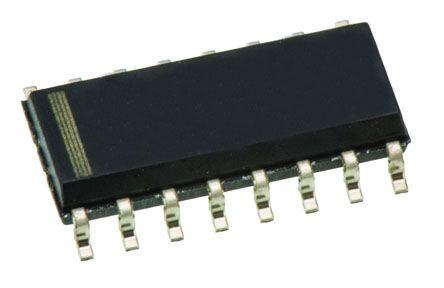
| 描述 | IC SWITCH 4CH I2C/SMBUS 16-SOIC多路器开关 IC 4-Ch I2C & SMBus Multiplexer |
| 产品分类 | |
| 品牌 | Texas Instruments |
| 产品手册 | |
| 产品图片 |
|
| rohs | 符合RoHS无铅 / 符合限制有害物质指令(RoHS)规范要求 |
| 产品系列 | 开关 IC,多路器开关 IC,Texas Instruments PCA9546ADW- |
| 数据手册 | |
| 产品型号 | PCA9546ADW |
| PCN设计/规格 | |
| 产品种类 | 多路器开关 IC |
| 传播延迟时间 | 1 ns |
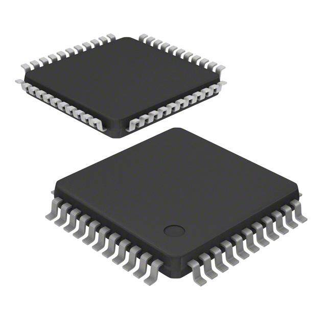
| 供应商器件封装 | 16-SOIC |
| 其它名称 | 296-33507-5 |
| 包装 | 管件 |
| 单位重量 | 420.400 mg |
| 商标 | Texas Instruments |
| 安装类型 | 表面贴装 |
| 安装风格 | SMD/SMT |
| 导通电阻—最大值 | 45 Ohms |
| 封装 | Tube |
| 封装/外壳 | 16-SOIC(0.295",7.50mm 宽) |
| 封装/箱体 | SOIC-16 Wide |
| 工作电源电压 | 2.3 V to 5.5 V |
| 工作电源电流 | 3 uA |
| 工厂包装数量 | 40 |
| 带宽 | 400 kHz |
| 应用 | 转换开关 |
| 开关数量 | 1 |
| 开关配置 | SPST |
| 接口 | I²C, SMBus |
| 最大功率耗散 | 400 mW |
| 最大工作温度 | + 85 C |
| 最小工作温度 | - 40 C |
| 标准包装 | 40 |
| 电压-电源 | 2.3 V ~ 5.5 V |
| 系列 | PCA9546A |
| 通道数量 | 4 Channel |

.jpg)


- 商务部:美国ITC正式对集成电路等产品启动337调查
- 曝三星4nm工艺存在良率问题 高通将骁龙8 Gen1或转产台积电
- 太阳诱电将投资9.5亿元在常州建新厂生产MLCC 预计2023年完工
- 英特尔发布欧洲新工厂建设计划 深化IDM 2.0 战略
- 台积电先进制程称霸业界 有大客户加持明年业绩稳了
- 达到5530亿美元!SIA预计今年全球半导体销售额将创下新高
- 英特尔拟将自动驾驶子公司Mobileye上市 估值或超500亿美元
- 三星加码芯片和SET,合并消费电子和移动部门,撤换高东真等 CEO
- 三星电子宣布重大人事变动 还合并消费电子和移动部门
- 海关总署:前11个月进口集成电路产品价值2.52万亿元 增长14.8%


PDF Datasheet 数据手册内容提取
Product Sample & Technical Tools & Support & Folder Buy Documents Software Community PCA9546A SCPS148G–OCTOBER2005–REVISEDMAY2016 2 PCA9546A Low Voltage 4-Channel I C and SMBus Switch with Reset Function 1 Features 2 Applications • 1-of-4BidirectionalTranslatingSwitches • Servers 1 • I2CBusandSMBusCompatible • Routers(TelecomSwitchingEquipment) • Active-LowResetInput • FactoryAutomation • ThreeAddressPins,AllowinguptoEight • ProductsWithI2CSlaveAddressConflicts PCA9546ADevicesontheI2CBus (forexample.Multiple,IdenticalTempSensors) • ChannelSelectionViaI2CBus,inAny 3 Description Combination The PCA9546A is a quad bidirectional translating • Power-upWithAllSwitchChannelsDeselected switch controlled via the I2C bus. The SCL/SDA • LowR Switches ON upstream pair fans out to four downstream pairs, or • AllowsVoltage-LevelTranslationBetween channels. Any individual SCn/SDn channel or 1.8-V,2.5-V,3.3-V,and5-VBuses combination of channels can be selected, determined • NoGlitchonPower-up bythecontentsoftheprogrammablecontrolregister. • SupportsHotInsertion An active-low reset (RESET) input allows the PCA9546Atorecoverfromasituationinwhichoneof • LowStandbyCurrent the downstream I2C buses is stuck in a low state. • OperatingPower-SupplyVoltageRangeof2.3V Pulling RESET low resets the I2C state machine and to5.5V causesallthechannelstobedeselected,asdoesthe • 5.5VTolerantInputs internalpower-onresetfunction. • 0to400-kHzClockFrequency The pass gates of the switches are constructed such • Latch-UpPerformanceExceeds100mAPer that the V pin can be used to limit the maximum CC JESD78 high voltage, which will be passed by the PCA9546A. This allows the use of different bus voltages on each • ESDProtectionExceedsJESD22 pair, so that 1.8-V, 2.5-V, or 3.3-V parts can – 2000-VHuman-BodyModel(A114-A) communicate with 5-V parts without any additional – 1000-VCharged-DeviceModel(C101) protection. External pull-up resistors pull the bus up to the desired voltage level for each channel. All I/O pinsare5.5-Vtolerant. DeviceInformation(1) PARTNUMBER PACKAGE BODYSIZE(NOM) PCA9546A TSSOP(16) 5.00mmx4.40mm (1) Forallavailablepackages,seetheorderableaddendumat theendofthedatasheet. SimplifiedApplicationDiagram SDA VCC SD0 Channel 0 SlavesA0,A1...AN I2C or SMBus SCL SC0 Master Channel 1 (e.g. Processor) RESET SD1 Slaves B0, B1...BN SC1 PCA9546A Channel 2 A0 SD2 Slaves C0, C1...CN SC2 A1 A2 Channel 3 GND SD3 Slaves D0, D1...DN SC3 Copyright © 2016,Texas Instruments Incorporated 1 An IMPORTANT NOTICE at the end of this data sheet addresses availability, warranty, changes, use in safety-critical applications, intellectualpropertymattersandotherimportantdisclaimers.PRODUCTIONDATA.
PCA9546A SCPS148G–OCTOBER2005–REVISEDMAY2016 www.ti.com Table of Contents 1 Features.................................................................. 1 8.3 FeatureDescription.................................................11 2 Applications........................................................... 1 8.4 DeviceFunctionalModes........................................11 3 Description............................................................. 1 8.5 Programming...........................................................11 8.6 ControlRegister......................................................14 4 RevisionHistory..................................................... 2 9 ApplicationandImplementation........................ 15 5 PinConfigurationandFunctions......................... 3 9.1 ApplicationInformation............................................15 6 Specifications......................................................... 4 9.2 TypicalApplication..................................................15 6.1 AbsoluteMaximumRatings .....................................4 10 PowerSupplyRecommendations..................... 19 6.2 ESDRatings ............................................................4 10.1 Power-OnResetErrata.........................................19 6.3 RecommendedOperatingConditions......................4 11 Layout................................................................... 19 6.4 ElectricalCharacteristics...........................................5 6.5 I2CInterfaceTimingRequirements..........................5 11.1 LayoutGuidelines.................................................19 6.6 InterruptandResetTimingRequirements................7 11.2 LayoutExample....................................................20 6.7 SwitchingCharacteristics..........................................7 12 DeviceandDocumentationSupport................. 20 7 ParameterMeasurementInformation..................8 12.1 ElectrostaticDischargeCaution............................20 12.2 Glossary................................................................20 8 DetailedDescription............................................ 10 13 Mechanical,Packaging,andOrderable 8.1 Overview.................................................................10 Information........................................................... 20 8.2 FunctionalBlockDiagram.......................................10 4 Revision History NOTE:Pagenumbersforpreviousrevisionsmaydifferfrompagenumbersinthecurrentversion. ChangesfromRevisionF(April2014)toRevisionG Page • Revisedpackmaterialaddendum;pin1quadrant .............................................................................................................. 20 ChangesfromRevisionE(January2008)toRevisionF Page • AddedRESETErratasection............................................................................................................................................... 11 • AddedPower-OnResetErratasection................................................................................................................................ 19 2 SubmitDocumentationFeedback Copyright©2005–2016,TexasInstrumentsIncorporated ProductFolderLinks:PCA9546A
PCA9546A www.ti.com SCPS148G–OCTOBER2005–REVISEDMAY2016 5 Pin Configuration and Functions RGV PACKAGE RGY PACKAGE D,DGV,DW,OR PW PACKAGE (TOPVIEW) (TOPVIEW) (TOPVIEW) A A1 A0 VCC SD A0 VCC A0 1 16 V CC 16 15 14 13 1 16 A1 2 15 SDA A1 2 15 SDA RESET 1 12 SCL RESET 3 14 SCL RESET 3 14 SCL SD0 2 11 A2 SD0 4 13 A2 SD0 4 13 A2 SC0 5 12 SC3 SC0 5 12 SC3 SC0 3 10 SC3 SD1 6 11 SD3 SD1 6 11 SD3 SD1 4 9 SD3 SC1 7 10 SC2 SC1 7 10 SC2 5 6 7 8 8 9 GND 8 9 SD2 1 D 2 2 D 2 C N D C N D S G S S G S PinFunctions PIN NO. DESCRIPTION NAME D,DGV,DW, RGV PW,ANDRGY A0 1 15 Addressinput0.ConnectdirectlytoV orground CC A1 2 16 Addressinput1.ConnectdirectlytoV orground CC A2 13 11 Addressinput2.ConnectdirectlytoV orground CC GND 8 6 Ground Activelowresetinput.ConnecttoV (1)throughapull-upresistor,ifnot RESET 3 1 DPUM used. SD0 4 2 Serialdata0.ConnecttoV (1)throughapull-upresistor DPU0 SC0 5 3 Serialclock0.ConnecttoV (1)throughapull-upresistor DPU0 SD1 6 4 Serialdata1.ConnecttoV (1)throughapull-upresistor DPU1 SC1 7 5 Serialclock1.ConnecttoV (1)throughapull-upresistor DPU1 SD2 9 7 Serialdata2.ConnecttoV (1)throughapull-upresistor DPU2 SC2 10 8 Serialclock2.ConnecttoV (1)throughapull-upresistor DPU2 SD3 11 9 Serialdata3.ConnecttoV (1)throughapull-upresistor. DPU3 SC3 12 10 Serialclock3.ConnecttoV (1)throughapull-upresistor DPU3 SCL 14 12 Serialclockline.ConnecttoV (1)throughapull-upresistor DPUM SDA 15 13 Serialdataline.ConnecttoV (1)throughapull-upresistor DPUM V 16 14 Supplypower CC (1) V isthepull-upreferencevoltagefortheassociateddataline.V isthemasterI2CreferencevoltagewhileV -V are DPUX DPUM DPU0 DPU3 theslavechannelreferencevoltages. Copyright©2005–2016,TexasInstrumentsIncorporated SubmitDocumentationFeedback 3 ProductFolderLinks:PCA9546A
PCA9546A SCPS148G–OCTOBER2005–REVISEDMAY2016 www.ti.com 6 Specifications 6.1 Absolute Maximum Ratings(1) overoperatingfree-airtemperaturerange(unlessotherwisenoted) MIN MAX UNIT V Supplyvoltage –0.5 7 V CC V Inputvoltage (2) –0.5 7 V I I Inputcurrent ±20 mA I I Outputcurrent ±25 mA O ContinuouscurrentthroughV ±100 mA CC ContinuouscurrentthroughGND ±100 mA Dpackage 73 DGVpackage 120 DWpackage 57 θ Packagethermalimpedance(3) °C/W JA PWpackage 108 RGVpackage 51.38 RGYpackage 50 P Totalpowerdissipation 400 mW tot T Operatingfree-airtemperature –40 85 °C A T Storagetemperature –65 150 stg (1) StressesbeyondthoselistedunderAbsoluteMaximumRatingsmaycausepermanentdamagetothedevice.Thesearestressratings only,whichdonotimplyfunctionaloperationofthedeviceattheseoranyotherconditionsbeyondthoseindicatedunderRecommended OperatingConditions.Exposuretoabsolute-maximum-ratedconditionsforextendedperiodsmayaffectdevicereliability. (2) Theinputnegative-voltageandoutputvoltageratingsmaybeexceedediftheinputandoutputcurrentratingsareobserved. (3) ThepackagethermalimpedanceiscalculatedinaccordancewithJESD51-7. 6.2 ESD Ratings VALUE UNIT Human-bodymodel(HBM),perANSI/ESDA/JEDECJS-001(1) ±2000 V(ESD) Electrostaticdischarge Charged-devicemodel(CDM),perJEDECspecificationJESD22- V C101(2) ±1000 (1) JEDECdocumentJEP155statesthat500-VHBMallowssafemanufacturingwithastandardESDcontrolprocess. (2) JEDECdocumentJEP157statesthat250-VCDMallowssafemanufacturingwithastandardESDcontrolprocess. 6.3 Recommended Operating Conditions(1) MIN MAX UNIT V Supplyvoltage 2.3 5.5 V CC SCL,SDA 0.7×V 6 CC V High-levelinputvoltage V IH A2–A0,RESET 0.7×V V +0.5 CC CC SCL,SDA –0.5 0.3×V CC V Low-levelinputvoltage V IL A2–A0,RESET –0.5 0.3×V CC T Operatingfree-airtemperature –40 85 °C A (1) AllunusedinputsofthedevicemustbeheldatV orGNDtoensureproperdeviceoperation.RefertotheTIapplicationreport, CC ImplicationsofSloworFloatingCMOSInputs,SCBA004. 4 SubmitDocumentationFeedback Copyright©2005–2016,TexasInstrumentsIncorporated ProductFolderLinks:PCA9546A
PCA9546A www.ti.com SCPS148G–OCTOBER2005–REVISEDMAY2016 6.4 Electrical Characteristics overrecommendedoperatingfree-airtemperaturerange(unlessotherwisenoted) PARAMETER TESTCONDITIONS V MIN TYP(1) MAX UNIT CC V Power-onresetvoltage(2) Noload, V =V orGND V 1.6 2.1 V POR I CC POR 5V 3.6 4.5Vto5.5V 2.6 4.5 3.3V 1.9 V Switchoutputvoltage V =V , I =–100μA V pass SWin CC SWout 3Vto3.6V 1.6 2.8 2.5V 1.5 2.3Vto2.7V 1.1 2 V =0.4V 3 7 OL I SCL,SDA 2.3Vto5.5V mA OL V =0.6V 6 10 OL SCL,SDA ±1 SC3–SC0,SD3–SD0 ±1 I V =V orGND 2.3Vto5.5V μA I I CC A2–A0 ±1 RESET ±1 5.5V 3 12 Operatingmode f =100kHz V =V orGND, I =0 3.6V 3 11 SCL I CC O 2.7V 3 10 5.5V 0.3 1 I Lowinputs V =GND, I =0 3.6V 0.1 1 μA CC I O 2.7V 0.1 1 Standbymode 5.5V 0.3 1 Highinputs V =V , I =0 3.6V 0.1 1 I CC O 2.7V 0.1 1 SCLorSDAinputat0.6V, 8 15 Supply-current OtherinputsatVCCorGND ΔI SCL,SDA μA CC change SCLorSDAinputatV –0.6V, CC 2.3Vto5.5V 8 15 OtherinputsatV orGND CC A2–A0 4.5 6 C V =V orGND 2.3Vto5.5V pF i I CC RESET 4.5 5.5 C SCL,SDA 15 19 (3i)o(OFF) VI=VCCorGND, SwitchOFF 2.3Vto5.5V pF SC3–SC0,SD3–SD0 6 8 4.5Vto5.5V 4 9 16 V =0.4V, I =15mA O O R Switchon-stateresistance 3Vto3.6V 5 11 20 Ω ON V =0.4V, I =10mA 2.3Vto2.7V 7 16 45 O O (1) Alltypicalvaluesareatnominalsupplyvoltage(2.5-V,3.3-V,or5-VV ),T =25°C. CC A (2) Thepower-onresetcircuitresetstheI2CbuslogicwithV <V .V mustbeloweredto0.2Vtoresetthedevice. CC POR CC (3) C dependsoninternalcapacitanceandexternalcapacitanceaddedtotheSCnlineswhenchannels(s)areON. io(ON) 6.5 I2C Interface Timing Requirements overrecommendedoperatingfree-airtemperaturerange(unlessotherwisenoted)(seeFigure1) MIN MAX UNIT I2CBUS—STANDARDMODE f I2Cclockfrequency 0 100 kHz scl t I2Cclockhightime 4 µs sch t I2Cclocklowtime 4.7 µs scl t I2Cspiketime 50 ns sp t I2Cserial-datasetuptime 250 ns sds Copyright©2005–2016,TexasInstrumentsIncorporated SubmitDocumentationFeedback 5 ProductFolderLinks:PCA9546A
PCA9546A SCPS148G–OCTOBER2005–REVISEDMAY2016 www.ti.com I2C Interface Timing Requirements (continued) overrecommendedoperatingfree-airtemperaturerange(unlessotherwisenoted)(seeFigure1) MIN MAX UNIT t I2Cserial-dataholdtime 0(1) ns sdh t I2Cinputrisetime 1000 ns icr t I2Cinputfalltime 300 ns icf t I2Coutputfalltime 10-pFto400-pFbus 300 ns ocf t I2Cbusfreetimebetweenstopandstart 4.7 µs buf t I2Cstartorrepeatedstartconditionsetup 4.7 µs sts t I2Cstartorrepeatedstartconditionhold 4 µs sth t I2Cstopconditionsetup 4 µs sps t Validdatatime(hightolow)(2) SCLlowtoSDAoutputlowvalid 1 µs vdL(Data) t Validdatatime(lowtohigh)(2) SCLlowtoSDAoutputhighvalid 0.6 µs vdH(Data) ACKsignalfromSCLlowto t ValiddatatimeofACKcondition 1 µs vd(ack) SDA(out)low C I2Cbuscapacitiveload 400 pF b (1) Adeviceinternallymustprovideaholdtimeofatleast300nsfortheSDAsignal(referredtotheV minoftheSCLsignal),inorderto IH bridgetheundefinedregionofthefallingedgeofSCL. (2) Datatakenusinga1-kΩpull-upresistorand50-pFload(seeFigure1) MIN MAX UNIT I2CBUS—FASTMODE f I2Cclockfrequency 0 400 kHz scl t I2Cclockhightime 0.6 µs sch t I2Cclocklowtime 1.3 µs scl t I2Cspiketime 50 ns sp t I2Cserial-datasetuptime 100 ns sds t I2Cserial-dataholdtime 0(1) ns sdh t I2Cinputrisetime 20+0.1C (2) 300 ns icr b t I2Cinputfalltime 20+0.1C (2) 300 ns icf b t I2Coutputfalltime 10-pFto400-pFbus 20+0.1C (2) 300 ns ocf b t I2Cbusfreetimebetweenstopandstart 1.3 µs buf t I2Cstartorrepeatedstartconditionsetup 0.6 µs sts t I2Cstartorrepeatedstartconditionhold 0.6 µs sth t I2Cstopconditionsetup 0.6 µs sps t Validdatatime(hightolow)(3) SCLlowtoSDAoutputlowvalid 1 µs vdL(Data) t Validdatatime(lowtohigh)(3) SCLlowtoSDAoutputhighvalid 0.6 vdH(Data) ACKsignalfromSCLlowto t ValiddatatimeofACKcondition 1 µs vd(ack) SDA(out)low C I2Cbuscapacitiveload 400 pF b (1) Adeviceinternallymustprovideaholdtimeofatleast300nsfortheSDAsignal(referredtotheV minoftheSCLsignal),inorderto IH bridgetheundefinedregionofthefallingedgeofSCL. (2) C =totalbuscapacitanceofonebuslineinpF b (3) Datatakenusinga1-kΩpull-upresistorand50-pFload(seeFigure1) 6 SubmitDocumentationFeedback Copyright©2005–2016,TexasInstrumentsIncorporated ProductFolderLinks:PCA9546A
PCA9546A www.ti.com SCPS148G–OCTOBER2005–REVISEDMAY2016 6.6 Interrupt and Reset Timing Requirements overrecommendedoperatingfree-airtemperaturerange(unlessotherwisenoted) PARAMETER MIN MAX UNIT t Pulseduration,RESETlow 6 ns WL t (1) RESETtime(SDAclear) 500 ns rst t RecoverytimefromRESETtostart 0 ns REC(STA) (1) t isthepropagationdelaymeasuredfromthetimetheRESETpinisfirstassertedlowtothetimetheSDApinisassertedhigh, rst signalingastopcondition.Itmustbeaminimumoft . WL 6.7 Switching Characteristics overrecommendedoperatingfree-airtemperaturerange,C ≤100pF(unlessotherwisenoted)(seeFigure1) L FROM TO PARAMETER MIN MAX UNIT (INPUT) (OUTPUT) R =20Ω,C =15pF 0.3 t (1) Propagationdelaytime ON L SDAorSCL SDnorSCn ns pd R =20Ω,C =50pF 1 ON L (1) ThepropagationdelayisthecalculatedRCtimeconstantofthetypicalON-stateresistanceoftheswitchandthespecifiedload capacitance,whendrivenbyanidealvoltagesource(zerooutputimpedance). Copyright©2005–2016,TexasInstrumentsIncorporated SubmitDocumentationFeedback 7 ProductFolderLinks:PCA9546A
PCA9546A SCPS148G–OCTOBER2005–REVISEDMAY2016 www.ti.com 7 Parameter Measurement Information V CC RL= 1 kΩ SDn, SCn DUT CL= 50 pF (See Note 1) Copyright © 2016,Texas Instruments Incorporated I2C PORT LOAD CONFIGURATION Two Bytes for Complete Device Programming Stop Start Address R/W Data Data Stop Address Address ACK ACK Condition Condition Bit 7 Bit 0 Bit 7 Bit 0 Condition Bit 6 Bit 1 (A) (A) (P) (S) (MSB) (LSB) (MSB) (LSB) (P) BYTE DESCRIPTION 1 I2C address + R/W 2 Control register data tscl tsch 0.7× VCC SCL 0.3× VCC tbuf ticr ticf tsp tovrd (ttAvvdCdLKH) tsts SDA 0.7× VCC 0.3× VCC ticf ticr tsdh tsps tsth tsds Repeat Start Stop Start or Repeat Condition Condition Start Condition VOLTAGE WAVEFORMS (1) C includesprobeandjigcapacitance. L (2) All input pulses are supplied by generators having the following characteristics: PRR ≤ 10 MHz, Z = 50 Ω, O t/t ≤30ns. r f (3) Theoutputsaremeasuredoneatatime,withonetransitionpermeasurement. Figure1. I2CInterfaceLoadCircuit,ByteDescriptions,andVoltageWaveforms 8 SubmitDocumentationFeedback Copyright©2005–2016,TexasInstrumentsIncorporated ProductFolderLinks:PCA9546A
PCA9546A www.ti.com SCPS148G–OCTOBER2005–REVISEDMAY2016 Parameter Measurement Information (continued) Start ACK or Read Cycle SCL SDA 30% trst RESET 50% tREC tWL Figure2. ResetTiming Copyright©2005–2016,TexasInstrumentsIncorporated SubmitDocumentationFeedback 9 ProductFolderLinks:PCA9546A
PCA9546A SCPS148G–OCTOBER2005–REVISEDMAY2016 www.ti.com 8 Detailed Description 8.1 Overview ThePCA9546Aisa4-channel,bidirectionaltranslatingI2Cswitch.ThemasterSCL/SDAsignalpairisdirectedto four channels of slave devices, SC0/SD0-SC3/SD3. Any individual downstream channel can be selected as well asanycombinationofthefourchannels. The device offers an active-low RESET input which resets the state machine and allows the PCA9546A to recover should one of the downstream I2C buses get stuck in a low state. The state machine of the device can alsoberesetbycyclingthepowersupply,V ,alsoknownasapower-onreset(POR).Boththe RESETfunction CC andaPORwillcauseallchannelstobedeselected. The connections of the I2C data path are controlled by the same I2C master device that is switched to communicate with multiple I2C slaves. After the successful acknowledgment of the slave address (hardware selectable by A0 and A1 pins), a single 8-bit control register is written to or read from to determine the selected channels. The PCA9546A may also be used for voltage translation, allowing the use of different bus voltages on each SCn/SDn pair such that 1.8-V, 2.5-V, or 3.3-V parts can communicate with 5-V parts. This is achieved by using externalpull-upresistorstopullthebusuptothedesiredvoltageforthemasterandeachslavechannel. 8.2 Functional Block Diagram PCA9546A 5 SC0 7 SC1 10 SC2 12 SC3 4 SD0 6 SD1 9 SD2 11 SD3 8 Switch Control Logic GND 16 VCC 3 Power-On RESET Reset 14 SCL 1 A0 15 Input Filter I2C Bus Control 2 A1 SDA 13 A2 Copyright © 2016, Texas Instruments Incorporated 10 SubmitDocumentationFeedback Copyright©2005–2016,TexasInstrumentsIncorporated ProductFolderLinks:PCA9546A
PCA9546A www.ti.com SCPS148G–OCTOBER2005–REVISEDMAY2016 8.3 Feature Description The PCA9546A is a 4-channel, bidirectional translating switch for I2C buses that supports Standard-Mode (100 kHz)andFast-Mode(400kHz)operation.ThePCA9546AfeaturesI2Ccontrolusingasingle8-bitcontrolregister in which the four least significant bits control the enabling and disabling of the 4 switch channels of I2C data flow. Depending on the application, voltage translation of the I2C bus can also be achieved using the PCA9546A to allow1.8-V,2.5-V,or3.3-Vpartstocommunicatewith5-Vparts.Additionally,intheeventthatcommunicationon the I2C bus enters a fault state, the PCA9546A can be reset to resume normal operation using the RESET pin featureorbyapower-onresetwhichresultsfromcyclingpowertothedevice. 8.4 Device Functional Modes 8.4.1 RESETInput TheRESETinputisanactive-lowsignalthatmaybeusedtorecoverfromabus-faultcondition.Whenthissignal is asserted low for a minimum of t , the PCA9546A resets its registers and I2C state machine and deselects all WL channels.TheRESETinputmustbeconnectedtoV throughapull-upresistor. CC 8.4.1.1 RESETErrata IfRESETvoltagesethigherthanV ,currentwillflowfromRESETpintoV pin. CC CC SystemImpact V willbepulledaboveitsregularvoltagelevel CC SystemWorkaround DesignsuchthatRESETvoltageissameorlowerthanV CC 8.4.2 Power-OnReset When power is applied to V , an internal power-on reset holds the PCA9546A in a reset condition until V has CC CC reached V . At this point, the reset condition is released, and the PCA9546A registers and I2C state machine POR are initialized to their default states, all zeroes, causing all the channels to be deselected. Thereafter, V must CC beloweredbelowV toresetthedevice. POR SeethePower-OnResetErratasection. 8.5 Programming 8.5.1 I2CInterface The I2C bus is for two-way two-line communication between different ICs or modules. The two lines are a serial data line (SDA) and a serial clock line (SCL). Both lines must be connected to a positive supply via a pull-up resistor when connected to the output stages of a device. Data transfer can be initiated only when the bus is not busy. One data bit is transferred during each clock pulse. The data on the SDA line must remain stable during the high periodoftheclockpulse,aschangesinthedatalineatthistimeareinterpretedascontrolsignals(seeFigure3). SDA SCL Data Line Change Stable; of Data Data Valid Allowed Figure3. BitTransfer Copyright©2005–2016,TexasInstrumentsIncorporated SubmitDocumentationFeedback 11 ProductFolderLinks:PCA9546A
PCA9546A SCPS148G–OCTOBER2005–REVISEDMAY2016 www.ti.com Programming (continued) Both data and clock lines remain high when the bus is not busy. A high-to-low transition of the data line while the clock is high is defined as the start condition (S). A low-to-high transition of the data line while the clock is high is definedasthestopcondition(P)(seeFigure4). SDA SCL S P Start Condition Stop Condition Figure4. DefinitionofStartandStopConditions A device generating a message is a transmitter; a device receiving is the receiver. The device that controls the messageisthemaster,andthedevicesthatarecontrolledbythemasteraretheslaves(seeFigure5). SDA SCL Master Slave Master I2C Transmitter/ Slave Transmitter/ Master Transmitter/ Multiplexer Receiver Receiver Receiver Transmitter Receiver Slave Figure5. SystemConfiguration Thenumberofdatabytestransferredbetweenthestartandthestopconditionsfromtransmittertoreceiverisnot limited. Each byte of eight bits is followed by one acknowledge (ACK) bit. The transmitter must release the SDA linebeforethereceivercansendanACKbit. When a slave receiver is addressed, it must generate an ACK after the reception of each byte. Also, a master must generate an ACK after the reception of each byte that has been clocked out of the slave transmitter. The device that acknowledges must pull down the SDA line during the ACK clock pulse so that the SDA line is stable low during the high pulse of the ACK-related clock period (see Figure 6). Setup and hold times must be taken intoaccount. 12 SubmitDocumentationFeedback Copyright©2005–2016,TexasInstrumentsIncorporated ProductFolderLinks:PCA9546A
PCA9546A www.ti.com SCPS148G–OCTOBER2005–REVISEDMAY2016 Programming (continued) Data Output by Transmitter NACK Data Output by Receiver ACK SCL From Master 1 2 8 9 S Start Clock Pulse for ACK Condition Figure6. AcknowledgmentontheI2CBus DataistransmittedtothePCA9546AcontrolregisterusingthewritemodeshowninFigure7. Slave Address Control Register S 1 1 1 0 A2 A1 A0 0 A X X X X B3 B2 B1 B0 A P SDA Start Condition R/W ACK From Slave ACK From Slave Stop Condition Figure7. WriteControlRegister DataisreadfromthePCA9546AcontrolregisterusingthereadmodeshowninFigure8. Slave Address Control Register SDA S 1 1 1 0 A2 A1 A0 1 A 0 0 0 0 B3 B2 B1 B0 NA P Start Condition R/W ACK From Slave NACK From Master Stop Condition Figure8. ReadControlRegister Copyright©2005–2016,TexasInstrumentsIncorporated SubmitDocumentationFeedback 13 ProductFolderLinks:PCA9546A
PCA9546A SCPS148G–OCTOBER2005–REVISEDMAY2016 www.ti.com 8.6 Control Register 8.6.1 DeviceAddress Following a start condition, the bus master must output the address of the slave it is accessing. The address of the PCA9546A is shown in Figure 9. To conserve power, no internal pull-up resistors are incorporated on the hardware-selectableaddresspins,andtheymustbepulledhighorlow. Slave Address 1 1 1 0 A2 A1 A0 R/W Fixed Hardware Selectable Figure9. PCA9546AAddress The last bit of the slave address defines the operation to be performed. When set to a logic 1, a read is selected, whilealogic0selectsawriteoperation. 8.6.2 ControlRegisterDescription Following the successful acknowledgment of the slave address, the bus master sends a byte to the PCA9546A, whichisstoredinthecontrolregister(seeFigure10).IfmultiplebytesarereceivedbythePCA9546A,itwillsave thelastbytereceived.ThisregistercanbewrittenandreadviatheI2Cbus. Channel Selection Bits (Read/Write) 7 6 5 4 3 2 1 0 X X X X B3 B2 B1 B0 Channel 0 Channel 1 Channel 2 Channel 3 Figure10. ControlRegister 8.6.3 ControlRegisterDefinition One or several SCn/SDn downstream pairs, or channels, are selected by the contents of the control register (see Table 1). This register is written after the PCA9546A has been addressed. The four LSBs of the control byte are used to determine which channel or channels are to be selected. When a channel is selected, the channel becomesactiveafterastopconditionhasbeenplacedontheI2Cbus.ThisensuresthatallSCn/SDnlinesarein a high state when the channel is made active, so that no false conditions are generated at the time of connection.Astopconditionalwaysmustoccurrightaftertheacknowledgecycle. 14 SubmitDocumentationFeedback Copyright©2005–2016,TexasInstrumentsIncorporated ProductFolderLinks:PCA9546A
PCA9546A www.ti.com SCPS148G–OCTOBER2005–REVISEDMAY2016 Control Register (continued) Table1.ControlRegisterWrite(ChannelSelection),ControlRegisterRead(ChannelStatus)(1) B7 B6 B5 B4 B3 B2 B1 B0 COMMAND 0 Channel0disabled X X X X X X X 1 Channel0enabled 0 Channel1disabled X X X X X X X 1 Channel1enabled 0 Channel2disabled X X X X X X X 1 Channel2enabled 0 Channel3disabled X X X X X X X 1 Channel3enabled Nochannelselected, 0 0 0 0 0 0 0 0 power-up/resetdefaultstate (1) Severalchannelscanbeenabledatthesametime.Forexample,B3=0,B2=1,B1=1,B0=0meansthatchannels0and3are disabled,andchannels1and2areenabled.Caremustbetakennottoexceedthemaximumbuscapacity. 9 Application and Implementation 9.1 Application Information Applications of the PCA9546A will contain an I2C (or SMBus) master device and up to four I2C slave devices. The downstream channels are ideally used to resolve I2C slave address conflicts. For example, if four identical digital temperature sensors are needed in the application, one sensor can be connected at each channel: 0, 1, 2, and3.Whenthetemperatureataspecificlocationmustberead,theappropriatechannelcanbeenabledandall other channels switched off, the data can be retrieved, and the I2C master can move on and read the next channel. In an application where the I2C bus will contain many additional slave devices that do not result in I2C slave address conflicts, these slave devices can be connected to any desired channel to distribute the total bus capacitance across multiple channels. If multiple switches will be enabled simultaneously, additional design requirementsmustbeconsidered(SeeDesignRequirementsandDetailedDesignProcedure). 9.2 Typical Application A typical application of the PCA9546A will contain anywhere from 1 to 5 separate data pull-up voltages, V , DPUX one for the master device (V ) and one for each of the selectable slave channels (V – V ). In the DPUM DPU0 DPU3 event where the master device and all slave devices operate at the same voltage, then the pass voltage, V = pass V . Once the maximum V is known, V can be selected easily using Figure 12. In an application where DPUX pass CC voltagetranslationisnecessary,additionaldesignrequirementsmustbeconsidered(SeeDesignRequirements). Figure11showsanapplicationinwhichthePCA9546Acanbeused. Copyright©2005–2016,TexasInstrumentsIncorporated SubmitDocumentationFeedback 15 ProductFolderLinks:PCA9546A
PCA9546A SCPS148G–OCTOBER2005–REVISEDMAY2016 www.ti.com Typical Application (continued) V = 2.3 V to 5.5 V DPUM VCC= 3.3 V V = 2.3 V to 5.5 V DPU0 16 VCC 15 4 SDA SDA SD0 I2C/SMBus 14 5 Channel 0 SCL SCL SC0 Master 3 V = 2.3 V to 5.5 V RESET DPU1 SD1 6 7 Channel 1 SC1 V = 2.3 V to 5.5 V PCA9546A DPU2 9 SD2 10 Channel 2 SC2 V = 2.3 V to 5.5 V DPU3 13 A2 2 A1 11 81 AG0ND SSDC33 12 Channel 3 Copyright © 2016,Texas Instruments Incorporated Figure11. PCA9546ATypicalApplicationSchematic 16 SubmitDocumentationFeedback Copyright©2005–2016,TexasInstrumentsIncorporated ProductFolderLinks:PCA9546A
PCA9546A www.ti.com SCPS148G–OCTOBER2005–REVISEDMAY2016 Typical Application (continued) 9.2.1 DesignRequirements TheA0,A1,andA2pinsarehardwareselectabletocontroltheslaveaddressofthePCA9546A.Thesepinsmay betieddirectlytoGNDorV intheapplication. CC If multiple slave channels will be activated simultaneously in the application, then the total I from SCL/SDA to OL GNDonthemastersidewillbethesumofthecurrentsthroughallpull-upresistors,R . p The pass-gate transistors of the PCA9546A are constructed such that the V voltage can be used to limit the CC maximumvoltagethatispassedfromoneI2Cbustoanother. Figure12showsthevoltagecharacteristicsofthepass-gatetransistors(notethatthegraphwasgeneratedusing data specified in the Electrical Characteristics section of this data sheet). In order for the PCA9546A to act as a voltage translator, the V voltage must be equal to or lower than the lowest bus voltage. For example, if the pass mainbusisrunningat5Vandthedownstreambusesare3.3Vand2.7V,V mustbeequaltoorbelow2.7V pass toeffectivelyclampthedownstreambusvoltages.AsshowninFigure12,V is2.7VwhenthePCA9546A pass(max) supply voltage is 4 V or lower, so the PCA9546A supply voltage could be set to 3.3 V. Pull-up resistors then can beusedtobringthebusvoltagestotheirappropriatelevels(seeFigure11). 9.2.2 DetailedDesignProcedure Once all the slaves are assigned to the appropriate slave channels and bus voltages are identified, the pull-up resistors, R , for each of the buses need to be selected appropriately. The minimum pull-up resistance is a p functionofV ,V ,andI asshowninEquation1: DPUX OL,(max) OL V -V R = DPUX OL(max) p(min) I OL (1) Themaximumpull-upresistanceisafunctionofthemaximumrisetime,t (300nsforfast-modeoperation,f = r SCL 400kHz)andbuscapacitance,C asshowninEquation2: b t = r R p(max) ´ 0.8473 C b (2) The maximum bus capacitance for an I2C bus must not exceed 400 pF for fast-mode operation. The bus capacitance can be approximated by adding the capacitance of the PCA9546A, C , the capacitance of io(OFF) wires/connections/traces, and the capacitance of each individual slave on a given channel. If multiple channels willbeactivatedsimultaneously,eachoftheslavesonallchannelswillcontributetototalbuscapacitance. Copyright©2005–2016,TexasInstrumentsIncorporated SubmitDocumentationFeedback 17 ProductFolderLinks:PCA9546A
PCA9546A SCPS148G–OCTOBER2005–REVISEDMAY2016 www.ti.com Typical Application (continued) 9.2.3 PCA9546AApplicationCurves 5 25 Standard-mode 4.5 Fast-mode Maximum 20 4 (V)s 3.5 Typical hm) 15 Vpas 2.35 (kOmax) 10 2 Rp( Minimum 1.5 5 1 2 2.5 3 3.5 4 4.5 5 5.5 0 VCC (V) 0 50 100 150 200 250 300 350 400 450 Space Space Cb (pF) D008 Standard-mode Fast-mode space space space space (f =100kHz,t =1µs) (f =400kHz,t=300ns) SCL r SCL r Figure12.Pass-GateVoltage(V )vsSupplyVoltage pass Figure13.MaximumPull-Upresistance(R )vsBus (V )atThreeTemperaturePoints p(max) CC Capacitance(C ) b 1.8 1.6 1.4 m) 1.2 h O 1 k (min) 0.8 Rp( 0.6 0.4 0.2 VDPUX > 2V VDPUX <= 2 0 0 0.5 1 1.5 2 2.5 3 3.5 4 4.5 5 5.5 VDPUX (V) D009 V =0.2×V ,I =2mAwhenV ≤2V OL DPUX OL DPUX V =0.4V,I =3mAwhenV >2V OL OL DPUX Figure14.MinimumPull-UpResistance(R )vsPull-UpReferenceVoltage(V ) p(min) DPUX 18 SubmitDocumentationFeedback Copyright©2005–2016,TexasInstrumentsIncorporated ProductFolderLinks:PCA9546A
PCA9546A www.ti.com SCPS148G–OCTOBER2005–REVISEDMAY2016 10 Power Supply Recommendations The operating power-supply voltage range of the PCA9546A is 2.3 V to 5.5 V applied at the V pin. When the CC PCA9546A is powered on for the first time or anytime the device must be reset by cycling the power supply, the power-onresetrequirementsmustbefollowedtoensuretheI2Cbuslogicisinitializedproperly. 10.1 Power-On Reset Errata Apower-onresetconditioncanbemissediftheV rampsareoutsidespecificationlistedinFigure15. CC Figure15. Power-OnResetCycle SystemImpact Iframpconditionsareoutsidetimingallowancesabove,PORconditioncanbemissed,causingthedevicetolock up. 11 Layout 11.1 Layout Guidelines For PCB layout of the PCA9546A, common PCB layout practices must be followed but additional concerns related to high-speed data transfer such as matched impedances and differential pairs are not a concern for I2C signal speeds. It is common to have a dedicated ground plane on an inner layer of the board and pins that are connectedtogroundmusthavealow-impedancepathtothegroundplaneintheformofwidepolygonpoursand multiple vias. By-pass and de-coupling capacitors are commonly used to control the voltage on the V pin, CC using a larger capacitor to provide additional power in the event of a short power supply glitch and a smaller capacitortofilterouthigh-frequencyripple. In an application where voltage translation is not required, all V voltages and V could be at the same DPUX CC potential and a single copper plane could connect all of pull-up resistors to the appropriate reference voltage. In an application where voltage translation is required, V , V , V , V , and V may all be on the DPUM DPU0 DPU1 DPU2 DPU3 samelayeroftheboardwithsplitplanestoisolatedifferentvoltagepotentials. To reduce the total I2C bus capacitance added by PCB parasitics, data lines (SCn and SDn) must be a short as possibleandthewidthsofthetracesmustalsobeminimized(e.g.5-10milsdependingoncopperweight). Copyright©2005–2016,TexasInstrumentsIncorporated SubmitDocumentationFeedback 19 ProductFolderLinks:PCA9546A
PCA9546A SCPS148G–OCTOBER2005–REVISEDMAY2016 www.ti.com 11.2 Layout Example LEGEND Partial Power Plane Polygonal To I2C Master Copper Pour VIAto Power Plane VIAto GND Plane (Inner Layer) V DPUM By-pass/De-coupling capacitors V GND V DPU0 CC 0 el A0 VCC ann VDPU3 h A1 SDA C e To av RESET SCL S Sl la To SD0 A A2 ve C 6 h a 4 n SC0 SC3 n 5 e 9 l 3 SD1 A SD3 nnel 1 SC1 PC SC2 a ave Ch GGNNDD SD2 VDPU2 To S Sl la To V ve C DPU1 h a n n e l 2 12 Device and Documentation Support 12.1 Electrostatic Discharge Caution Thesedeviceshavelimitedbuilt-inESDprotection.Theleadsshouldbeshortedtogetherorthedeviceplacedinconductivefoam duringstorageorhandlingtopreventelectrostaticdamagetotheMOSgates. 12.2 Glossary SLYZ022—TIGlossary. Thisglossarylistsandexplainsterms,acronyms,anddefinitions. 13 Mechanical, Packaging, and Orderable Information Thefollowingpagesincludemechanical,packaging,andorderableinformation.Thisinformationisthemost currentdataavailableforthedesignateddevices.Thisdataissubjecttochangewithoutnoticeandrevisionof thisdocument.Forbrowser-basedversionsofthisdatasheet,refertotheleft-handnavigation 20 SubmitDocumentationFeedback Copyright©2005–2016,TexasInstrumentsIncorporated ProductFolderLinks:PCA9546A
PACKAGE OPTION ADDENDUM www.ti.com 6-Feb-2020 PACKAGING INFORMATION Orderable Device Status Package Type Package Pins Package Eco Plan Lead/Ball Finish MSL Peak Temp Op Temp (°C) Device Marking Samples (1) Drawing Qty (2) (6) (3) (4/5) PCA9546AD ACTIVE SOIC D 16 40 Green (RoHS NIPDAU Level-1-260C-UNLIM -40 to 85 PCA9546A & no Sb/Br) PCA9546ADGVR ACTIVE TVSOP DGV 16 2000 Green (RoHS NIPDAU Level-1-260C-UNLIM -40 to 85 PD546A & no Sb/Br) PCA9546ADR ACTIVE SOIC D 16 2500 Green (RoHS NIPDAU Level-1-260C-UNLIM -40 to 85 PCA9546A & no Sb/Br) PCA9546ADT ACTIVE SOIC D 16 250 Green (RoHS NIPDAU Level-1-260C-UNLIM -40 to 85 PCA9546A & no Sb/Br) PCA9546ADW ACTIVE SOIC DW 16 40 Green (RoHS NIPDAU Level-1-260C-UNLIM -40 to 85 PCA9546A & no Sb/Br) PCA9546ADWG4 ACTIVE SOIC DW 16 40 Green (RoHS NIPDAU Level-1-260C-UNLIM -40 to 85 PCA9546A & no Sb/Br) PCA9546ADWR ACTIVE SOIC DW 16 2000 Green (RoHS NIPDAU Level-1-260C-UNLIM -40 to 85 PCA9546A & no Sb/Br) PCA9546APW ACTIVE TSSOP PW 16 90 Green (RoHS NIPDAU Level-1-260C-UNLIM -40 to 85 PD546A & no Sb/Br) PCA9546APWE4 ACTIVE TSSOP PW 16 90 Green (RoHS NIPDAU Level-1-260C-UNLIM -40 to 85 PD546A & no Sb/Br) PCA9546APWR ACTIVE TSSOP PW 16 2000 Green (RoHS NIPDAU Level-1-260C-UNLIM -40 to 85 PD546A & no Sb/Br) PCA9546APWRE4 ACTIVE TSSOP PW 16 2000 Green (RoHS NIPDAU Level-1-260C-UNLIM -40 to 85 PD546A & no Sb/Br) PCA9546APWRG4 ACTIVE TSSOP PW 16 2000 Green (RoHS NIPDAU Level-1-260C-UNLIM -40 to 85 PD546A & no Sb/Br) PCA9546APWT ACTIVE TSSOP PW 16 250 Green (RoHS NIPDAU Level-1-260C-UNLIM -40 to 85 PD546A & no Sb/Br) PCA9546APWTG4 ACTIVE TSSOP PW 16 250 Green (RoHS NIPDAU Level-1-260C-UNLIM -40 to 85 PD546A & no Sb/Br) PCA9546ARGVR ACTIVE VQFN RGV 16 2500 Green (RoHS NIPDAU Level-2-260C-1 YEAR -40 to 85 PD546A & no Sb/Br) PCA9546ARGYR ACTIVE VQFN RGY 16 3000 Green (RoHS NIPDAU Level-2-260C-1 YEAR -40 to 85 PD546A & no Sb/Br) (1) The marketing status values are defined as follows: ACTIVE: Product device recommended for new designs. Addendum-Page 1
PACKAGE OPTION ADDENDUM www.ti.com 6-Feb-2020 LIFEBUY: TI has announced that the device will be discontinued, and a lifetime-buy period is in effect. NRND: Not recommended for new designs. Device is in production to support existing customers, but TI does not recommend using this part in a new design. PREVIEW: Device has been announced but is not in production. Samples may or may not be available. OBSOLETE: TI has discontinued the production of the device. (2) RoHS: TI defines "RoHS" to mean semiconductor products that are compliant with the current EU RoHS requirements for all 10 RoHS substances, including the requirement that RoHS substance do not exceed 0.1% by weight in homogeneous materials. Where designed to be soldered at high temperatures, "RoHS" products are suitable for use in specified lead-free processes. TI may reference these types of products as "Pb-Free". RoHS Exempt: TI defines "RoHS Exempt" to mean products that contain lead but are compliant with EU RoHS pursuant to a specific EU RoHS exemption. Green: TI defines "Green" to mean the content of Chlorine (Cl) and Bromine (Br) based flame retardants meet JS709B low halogen requirements of <=1000ppm threshold. Antimony trioxide based flame retardants must also meet the <=1000ppm threshold requirement. (3) MSL, Peak Temp. - The Moisture Sensitivity Level rating according to the JEDEC industry standard classifications, and peak solder temperature. (4) There may be additional marking, which relates to the logo, the lot trace code information, or the environmental category on the device. (5) Multiple Device Markings will be inside parentheses. Only one Device Marking contained in parentheses and separated by a "~" will appear on a device. If a line is indented then it is a continuation of the previous line and the two combined represent the entire Device Marking for that device. (6) Lead/Ball Finish - Orderable Devices may have multiple material finish options. Finish options are separated by a vertical ruled line. Lead/Ball Finish values may wrap to two lines if the finish value exceeds the maximum column width. Important Information and Disclaimer:The information provided on this page represents TI's knowledge and belief as of the date that it is provided. TI bases its knowledge and belief on information provided by third parties, and makes no representation or warranty as to the accuracy of such information. Efforts are underway to better integrate information from third parties. TI has taken and continues to take reasonable steps to provide representative and accurate information but may not have conducted destructive testing or chemical analysis on incoming materials and chemicals. TI and TI suppliers consider certain information to be proprietary, and thus CAS numbers and other limited information may not be available for release. In no event shall TI's liability arising out of such information exceed the total purchase price of the TI part(s) at issue in this document sold by TI to Customer on an annual basis. Addendum-Page 2
PACKAGE MATERIALS INFORMATION www.ti.com 26-Feb-2019 TAPE AND REEL INFORMATION *Alldimensionsarenominal Device Package Package Pins SPQ Reel Reel A0 B0 K0 P1 W Pin1 Type Drawing Diameter Width (mm) (mm) (mm) (mm) (mm) Quadrant (mm) W1(mm) PCA9546ADGVR TVSOP DGV 16 2000 330.0 12.4 6.8 4.0 1.6 8.0 12.0 Q1 PCA9546ADR SOIC D 16 2500 330.0 16.4 6.5 10.3 2.1 8.0 16.0 Q1 PCA9546ADWR SOIC DW 16 2000 330.0 16.4 10.75 10.7 2.7 12.0 16.0 Q1 PCA9546APWR TSSOP PW 16 2000 330.0 12.4 6.9 5.6 1.6 8.0 12.0 Q1 PCA9546APWT TSSOP PW 16 250 330.0 12.4 6.9 5.6 1.6 8.0 12.0 Q1 PCA9546ARGVR VQFN RGV 16 2500 330.0 12.4 4.25 4.25 1.15 8.0 12.0 Q2 PCA9546ARGYR VQFN RGY 16 3000 330.0 12.4 3.8 4.3 1.5 8.0 12.0 Q1 PackMaterials-Page1
PACKAGE MATERIALS INFORMATION www.ti.com 26-Feb-2019 *Alldimensionsarenominal Device PackageType PackageDrawing Pins SPQ Length(mm) Width(mm) Height(mm) PCA9546ADGVR TVSOP DGV 16 2000 367.0 367.0 35.0 PCA9546ADR SOIC D 16 2500 333.2 345.9 28.6 PCA9546ADWR SOIC DW 16 2000 350.0 350.0 43.0 PCA9546APWR TSSOP PW 16 2000 367.0 367.0 35.0 PCA9546APWT TSSOP PW 16 250 367.0 367.0 35.0 PCA9546ARGVR VQFN RGV 16 2500 367.0 367.0 35.0 PCA9546ARGYR VQFN RGY 16 3000 367.0 367.0 35.0 PackMaterials-Page2
None
None
PACKAGE OUTLINE PW0016A TSSOP - 1.2 mm max height SCALE 2.500 SMALL OUTLINE PACKAGE SEATING PLANE C 6.6 TYP 6.2 A 0.1 C PIN 1 INDEX AREA 14X 0.65 16 1 2X 5.1 4.55 4.9 NOTE 3 8 9 0.30 B 4.5 16X 0.19 1.2 MAX 4.3 0.1 C A B NOTE 4 (0.15) TYP SEE DETAIL A 0.25 GAGE PLANE 0.15 0.05 0.75 0.50 0 -8 DETA 20AIL A TYPICAL 4220204/A 02/2017 NOTES: 1. All linear dimensions are in millimeters. Any dimensions in parenthesis are for reference only. Dimensioning and tolerancing per ASME Y14.5M. 2. This drawing is subject to change without notice. 3. This dimension does not include mold flash, protrusions, or gate burrs. Mold flash, protrusions, or gate burrs shall not exceed 0.15 mm per side. 4. This dimension does not include interlead flash. Interlead flash shall not exceed 0.25 mm per side. 5. Reference JEDEC registration MO-153. www.ti.com
EXAMPLE BOARD LAYOUT PW0016A TSSOP - 1.2 mm max height SMALL OUTLINE PACKAGE 16X (1.5) SYMM (R0.05) TYP 1 16X (0.45) 16 SYMM 14X (0.65) 8 9 (5.8) LAND PATTERN EXAMPLE EXPOSED METAL SHOWN SCALE: 10X SOLDER MASK METAL UNDER SOLDER MASK OPENING METAL SOLDER MASK OPENING EXPOSED METAL EXPOSED METAL 0.05 MAX 0.05 MIN ALL AROUND ALL AROUND NON-SOLDER MASK SOLDER MASK DEFINED DEFINED (PREFERRED) SOLDE15.000R MASK DETAILS 4220204/A 02/2017 NOTES: (continued) 6. Publication IPC-7351 may have alternate designs. 7. Solder mask tolerances between and around signal pads can vary based on board fabrication site. www.ti.com
EXAMPLE STENCIL DESIGN PW0016A TSSOP - 1.2 mm max height SMALL OUTLINE PACKAGE 16X (1.5) SYMM (R0.05) TYP 1 16X (0.45) 16 SYMM 14X (0.65) 8 9 (5.8) SOLDER PASTE EXAMPLE BASED ON 0.125 mm THICK STENCIL SCALE: 10X 4220204/A 02/2017 NOTES: (continued) 8. Laser cutting apertures with trapezoidal walls and rounded corners may offer better paste release. IPC-7525 may have alternate design recommendations. 9. Board assembly site may have different recommendations for stencil design. www.ti.com
GENERIC PACKAGE VIEW DW 16 SOIC - 2.65 mm max height 7.5 x 10.3, 1.27 mm pitch SMALL OUTLINE INTEGRATED CIRCUIT This image is a representation of the package family, actual package may vary. Refer to the product data sheet for package details. 4224780/A www.ti.com
PACKAGE OUTLINE DW0016A SOIC - 2.65 mm max height SCALE 1.500 SOIC C 10.63 SEATING PLANE TYP 9.97 A PIN 1 ID 0.1 C AREA 14X 1.27 16 1 10.5 2X 10.1 8.89 NOTE 3 8 9 0.51 16X 0.31 7.6 B 7.4 0.25 C A B 2.65 MAX NOTE 4 0.33 TYP 0.10 SEE DETAIL A 0.25 GAGE PLANE 0.3 0 - 8 0.1 1.27 0.40 DETAIL A (1.4) TYPICAL 4220721/A 07/2016 NOTES: 1. All linear dimensions are in millimeters. Dimensions in parenthesis are for reference only. Dimensioning and tolerancing per ASME Y14.5M. 2. This drawing is subject to change without notice. 3. This dimension does not include mold flash, protrusions, or gate burrs. Mold flash, protrusions, or gate burrs shall not exceed 0.15 mm, per side. 4. This dimension does not include interlead flash. Interlead flash shall not exceed 0.25 mm, per side. 5. Reference JEDEC registration MS-013. www.ti.com
EXAMPLE BOARD LAYOUT DW0016A SOIC - 2.65 mm max height SOIC 16X (2) SEE SYMM DETAILS 1 16 16X (0.6) SYMM 14X (1.27) 8 9 R0.05 TYP (9.3) LAND PATTERN EXAMPLE SCALE:7X METAL SOLDER MASK SOLDER MASK METAL OPENING OPENING 0.07 MAX 0.07 MIN ALL AROUND ALL AROUND NON SOLDER MASK SOLDER MASK DEFINED DEFINED SOLDER MASK DETAILS 4220721/A 07/2016 NOTES: (continued) 6. Publication IPC-7351 may have alternate designs. 7. Solder mask tolerances between and around signal pads can vary based on board fabrication site. www.ti.com
EXAMPLE STENCIL DESIGN DW0016A SOIC - 2.65 mm max height SOIC 16X (2) SYMM 1 16 16X (0.6) SYMM 14X (1.27) 8 9 R0.05 TYP (9.3) SOLDER PASTE EXAMPLE BASED ON 0.125 mm THICK STENCIL SCALE:7X 4220721/A 07/2016 NOTES: (continued) 8. Laser cutting apertures with trapezoidal walls and rounded corners may offer better paste release. IPC-7525 may have alternate design recommendations. 9. Board assembly site may have different recommendations for stencil design. www.ti.com
None
None
None
None
None
None
IMPORTANTNOTICEANDDISCLAIMER TI PROVIDES TECHNICAL AND RELIABILITY DATA (INCLUDING DATASHEETS), DESIGN RESOURCES (INCLUDING REFERENCE DESIGNS), APPLICATION OR OTHER DESIGN ADVICE, WEB TOOLS, SAFETY INFORMATION, AND OTHER RESOURCES “AS IS” AND WITH ALL FAULTS, AND DISCLAIMS ALL WARRANTIES, EXPRESS AND IMPLIED, INCLUDING WITHOUT LIMITATION ANY IMPLIED WARRANTIES OF MERCHANTABILITY, FITNESS FOR A PARTICULAR PURPOSE OR NON-INFRINGEMENT OF THIRD PARTY INTELLECTUAL PROPERTY RIGHTS. These resources are intended for skilled developers designing with TI products. You are solely responsible for (1) selecting the appropriate TI products for your application, (2) designing, validating and testing your application, and (3) ensuring your application meets applicable standards, and any other safety, security, or other requirements. These resources are subject to change without notice. TI grants you permission to use these resources only for development of an application that uses the TI products described in the resource. Other reproduction and display of these resources is prohibited. No license is granted to any other TI intellectual property right or to any third party intellectual property right. TI disclaims responsibility for, and you will fully indemnify TI and its representatives against, any claims, damages, costs, losses, and liabilities arising out of your use of these resources. TI’s products are provided subject to TI’s Terms of Sale (www.ti.com/legal/termsofsale.html) or other applicable terms available either on ti.com or provided in conjunction with such TI products. TI’s provision of these resources does not expand or otherwise alter TI’s applicable warranties or warranty disclaimers for TI products. Mailing Address: Texas Instruments, Post Office Box 655303, Dallas, Texas 75265 Copyright © 2020, Texas Instruments Incorporated