 Datasheet下载
- 型号: PCA9540BDP,118
- 制造商: NXP Semiconductors
- 库位|库存: xxxx|xxxx
- 要求:
| 数量阶梯 | 香港交货 | 国内含税 |
| +xxxx | $xxxx | ¥xxxx |
查看当月历史价格
查看今年历史价格
PCA9540BDP,118产品简介:
ICGOO电子元器件商城为您提供PCA9540BDP,118由NXP Semiconductors设计生产,在icgoo商城现货销售,并且可以通过原厂、代理商等渠道进行代购。 PCA9540BDP,118价格参考。NXP SemiconductorsPCA9540BDP,118封装/规格:接口 - 专用, 2-Channel I²C Multiplexer Interface 8-TSSOP。您可以下载PCA9540BDP,118参考资料、Datasheet数据手册功能说明书,资料中有PCA9540BDP,118 详细功能的应用电路图电压和使用方法及教程。
PCA9540BDP 是由 NXP USA Inc. 生产的一款接口 - 专用芯片,具体型号为 PCA9540BDP,118。它是一款 I2C 总线开关,主要用于扩展 I2C 主控制器的通信能力,支持多路从设备的同时连接。以下是其主要应用场景:

 1. 多设备管理
   PCA9540BDP 提供两个可独立控制的 I2C 通道(子总线),允许主控制器根据需要选择与不同的从设备进行通信。这种功能在复杂的嵌入式系统中非常有用,例如工业自动化、智能家居和汽车电子等领域,当多个传感器或外设需要通过 I2C 接口连接到主控制器时。

 2. 减轻 I2C 总线负载
   在多设备连接的情况下,I2C 总线可能会因为过多的设备而导致信号干扰或速度下降。PCA9540BDP 可以将主控制器的 I2C 总线划分为多个子总线,从而减少每个子总线上的设备数量,降低总线负载,提高通信稳定性。

 3. 热插拔保护
   PCA9540BDP 支持热插拔功能,允许在系统运行时安全地添加或移除设备,而不会对其他设备或主控制器造成干扰。这一特性非常适合需要动态调整硬件配置的应用场景,例如模块化测试设备或便携式医疗设备。

 4. 汽车电子系统
   在现代汽车中,PCA9540BDP 可用于管理各种传感器和执行器的 I2C 通信,例如温度传感器、压力传感器、环境光传感器等。通过将这些设备分配到不同的子总线上,可以确保关键信号的优先级和可靠性。

 5. 消费电子设备
   在智能手机、平板电脑或其他消费电子产品中,PCA9540BDP 可用于管理触摸屏控制器、电源管理单元、摄像头模块等组件的 I2C 通信。它能够优化资源分配,提升系统的整体性能。

 6. 工业自动化
   在工业控制系统中,PCA9540BDP 能够帮助实现多节点的分布式控制。例如,在工厂的监控系统中,它可以用来管理不同区域的传感器和执行器,确保数据采集和控制指令的高效传输。

总之,PCA9540BDP 的主要作用是通过分时复用和多路切换技术,扩展 I2C 总线的通信能力,适用于需要高可靠性和灵活管理的多设备系统。
| 参数 | 数值 |
| 产品目录 | 集成电路 (IC)半导体 |
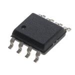
| 描述 | IC I2C MUX 2CH 8-TSSOP编码器、解码器、复用器和解复用器 I2C MUX 2CH |
| 产品分类 | |
| 品牌 | NXP Semiconductors |
| 产品手册 | |
| 产品图片 |
|
| rohs | 符合RoHS无铅 / 符合限制有害物质指令(RoHS)规范要求 |
| 产品系列 | 逻辑集成电路,编码器、解码器、复用器和解复用器,NXP Semiconductors PCA9540BDP,118- |
| 数据手册 | |
| 产品型号 | PCA9540BDP,118 |
| PCN封装 | |
| 产品 | Decoders, Encoders, Multiplexers & Demultiplexers |
| 产品培训模块 | http://www.digikey.cn/PTM/IndividualPTM.page?site=cn&lang=zhs&ptm=25410 |
| 产品目录页面 | |
| 产品种类 | 编码器、解码器、复用器和解复用器 |
| 传播延迟时间 | 0.3 ns |
| 供应商器件封装 | 8-TSSOP |
| 其它名称 | 568-1845-6 |
| 功率耗散 | 400 mW |
| 包装 | Digi-Reel® |
| 商标 | NXP Semiconductors |
| 安装类型 | 表面贴装 |
| 安装风格 | SMD/SMT |
| 封装 | Reel |
| 封装/外壳 | 8-TSSOP,8-MSOP(0.118",3.00mm 宽) |
| 封装/箱体 | SOT-505 |
| 工厂包装数量 | 2500 |
| 应用 | 2 通道 I²C 多路复用器 |
| 接口 | I²C |
| 最大工作温度 | + 85 C |
| 最小工作温度 | - 40 C |
| 标准包装 | 1 |
| 特色产品 | http://www.digikey.com/cn/zh/ph/NXP/I2C.html |
| 电压-电源 | 2.3 V ~ 5.5 V |
| 电源电压-最大 | 5.5 V |
| 电源电压-最小 | 2.3 V |
| 输入/输出线数量 | 1 / 2 |
| 输入线路数量 | 1 |
| 输出线路数量 | 2 |
| 逻辑系列 | PCA |
| 配用 | /product-detail/zh/OM6275,598/568-3615-ND/1154197 |
| 零件号别名 | PCA9540BDP-T |


- 商务部:美国ITC正式对集成电路等产品启动337调查
- 曝三星4nm工艺存在良率问题 高通将骁龙8 Gen1或转产台积电
- 太阳诱电将投资9.5亿元在常州建新厂生产MLCC 预计2023年完工
- 英特尔发布欧洲新工厂建设计划 深化IDM 2.0 战略
- 台积电先进制程称霸业界 有大客户加持明年业绩稳了
- 达到5530亿美元!SIA预计今年全球半导体销售额将创下新高
- 英特尔拟将自动驾驶子公司Mobileye上市 估值或超500亿美元
- 三星加码芯片和SET,合并消费电子和移动部门,撤换高东真等 CEO
- 三星电子宣布重大人事变动 还合并消费电子和移动部门
- 海关总署:前11个月进口集成电路产品价值2.52万亿元 增长14.8%


PDF Datasheet 数据手册内容提取
PCA9540B 2-channel I2C-bus multiplexer Rev. 7.1 — 19 January 2018 Product data sheet 1. General description The PCA9540B is a 1-of-2 bidirectional translating multiplexer, controlled via the I2C-bus. The SCL/SDA upstream pair fans out to two SCx/SDx downstream pairs, or channels. Only one SCx/SDx channel is selected at a time, determined by the contents of the programmable control register. A power-on reset function puts the registers in their default state and initializes the I2C-bus state machine with no channels selected. The pass gates of the multiplexer are constructed such that the V pin can be used to DD limit the maximum high voltage that is passed by the PCA9540B. This allows the use of different bus voltages on each SCx/SDx pair, so that 1.8V, 2.5V or 3.3V parts can communicate with 5V parts without any additional protection. External pull-up resistors can pull the bus up to the desired voltage level for this channel. All I/O pins are 5V tolerant. 2. Features and benefits 1-of-2 bidirectional translating multiplexer I2C-bus interface logic; compatible with SMBus standards Channel selection via I2C-bus Power-up with all multiplexer channels deselected Low R switches on Allows voltage level translation between 1.8V, 2.5V, 3.3V and 5V buses No glitch on power-up Supports hot insertion Low standby current Operating power supply voltage range of 2.3V to 5.5V 5V tolerant inputs 0Hz to 400kHz clock frequency ESD protection exceeds 2000V HBM per JESD22-A114, and 1000V CDM per JESD22-C101 Latch-up testing is done to JEDEC Standard JESD78 which exceeds 100mA Packages offered: SO8, TSSOP8, XSON8
PCA9540B NXP Semiconductors 2-channel I2C-bus multiplexer 3. Ordering information Table 1. Ordering info rmation Type number Topside Package marking Name Description Version PCA9540BD PA9540B SO8 plastic small outline package; 8leads; bodywidth3.9mm SOT96-1 PCA9540BDP 9540B TSSOP8 plastic thin shrink small outline package; 8leads; SOT505-1 bodywidth3mm PCA9540BDP/Q900 9540B TSSOP8 plastic thin shrink small outline package; 8leads; SOT505-1 bodywidth3mm PCA9540BGD 40B XSON8 plastic extremely thin small outline package; noleads; SOT996-2 8terminals; body320.5mm [1] PCA9540BDP/Q900 is AEC-Q100 compliant. Contact your NXP account team, distribution partner or i2c.support@nxp.com for PPAP. 3.1 Ordering options Table 2. Ordering opt ions Type number Orderable partnumber Package Packing method Minimum Temperature order range quantity PCA9540BD PCA9540BD,118 SO8 Reel 13” Q1/T1 2500 T =40C to amb *Standard mark SMD +85C PCA9540BDP PCA9540BDP,118 TSSOP8 Reel 13” Q1/T1 2500 T =40C to amb *Standard mark SMD +85C PCA9540BDP/Q900 PCA9540BDP/Q900,118 TSSOP8 Reel 13” Q1/T1 2500 T =40C to amb *Standard mark SMD +105C PCA9540BGD PCA9540BGD,125 XSON8 Reel 7” Q3/T4 3000 T =40C to amb *Standard mark +85C PCA9540B All information provided in this document is subject to legal disclaimers. © NXP Semiconductors N.V. 2018. All rights reserved. Product data sheet Rev. 7.1 — 19 January 2018 2 of 28
PCA9540B NXP Semiconductors 2-channel I2C-bus multiplexer 4. Block diagram PCA9540B SD0 SD1 SC0 SC1 VSS SWITCH CONTROL LOGIC POWER-ON VDD RESET SCL INPUT I2C-BUS FILTER SDA CONTROL 002aae715 Fig 1. Block diagram of PCA9540B PCA9540B All information provided in this document is subject to legal disclaimers. © NXP Semiconductors N.V. 2018. All rights reserved. Product data sheet Rev. 7.1 — 19 January 2018 3 of 28
PCA9540B NXP Semiconductors 2-channel I2C-bus multiplexer 5. Pinning information 5.1 Pinning SCL 1 8 SC1 SCL 1 8 SC1 SDA 2 7 SD1 SDA 2 7 SD1 PCA9540BD PCA9540BDP VDD 3 6 VSS VDD 3 6 VSS SD0 4 5 SC0 SD0 4 5 SC0 002aae713 002aae714 Fig 2. Pin configuration for SO8 Fig 3. Pin configuration for TSSOP8 SCL 1 8 SC1 SDA 2 7 SD1 PCA9540BGD VDD 3 6 VSS SD0 4 5 SC0 002aae753 Transparent top view Fig 4. Pin configuration for XSON8 5.2 Pin description Table 3. Pin description Symbol Pin Description SCL 1 serial clock line SDA 2 serial data line V 3 supply voltage DD SD0 4 serial data 0 SC0 5 serial clock 0 V 6 supply ground SS SD1 7 serial data 1 SC1 8 serial clock 1 PCA9540B All information provided in this document is subject to legal disclaimers. © NXP Semiconductors N.V. 2018. All rights reserved. Product data sheet Rev. 7.1 — 19 January 2018 4 of 28
PCA9540B NXP Semiconductors 2-channel I2C-bus multiplexer 6. Functional description Refer to Figure 1 “Block diagram of PCA9540B”. 6.1 Device addressing Following a START condition the bus master must output the address of the slave it is accessing. The address of the PCA9540B is shown in Figure5. slave address 1 1 1 0 0 0 0 R/W fixed 002aae716 Fig 5. Slave address The last bit of the slave address defines the operation to be performed. When set to logic1 a read is selected, while a logic0 selects a write operation. 6.2 Control register Following the successful acknowledgement of the slave address, the bus master sends a byte to the PCA9540B which is stored in the Control register. If multiple bytes are received by the PCA9540B, it saves the last byte received. This register can be written and read via the I2C-bus. channel selection bits (read/write) 7 6 5 4 3 2 1 0 X X X X X B2 B1 B0 002aae717 enable bit Fig 6. Control register 6.2.1 Control register definition A SCx/SDx downstream pair, or channel, is selected by the contents of the Control register. This register is written after the PCA9540B has been addressed. The 2LSBs of the control byte are used to determine which channel is to be selected. When a channel is selected, it will become active after a STOP condition has been placed on the I2C-bus. This ensures that all SCx/SDx lines are in a HIGH state when the channel is made active, so that no false conditions are generated at the time of connection. PCA9540B All information provided in this document is subject to legal disclaimers. © NXP Semiconductors N.V. 2018. All rights reserved. Product data sheet Rev. 7.1 — 19 January 2018 5 of 28
PCA9540B NXP Semiconductors 2-channel I2C-bus multiplexer Table 4. Control register: Write — channel selection; Read — channel status D7 D6 D5 D4 D3 B2 B1 B0 Command X X X X X 0 X X no channel selected X X X X X 1 0 0 channel0 enabled X X X X X 1 0 1 channel1 enabled X X X X X 1 1 X no channel selected 0 0 0 0 0 0 0 0 no channel selected; power-up default state 6.3 Power-on reset When power is applied to V , an internal Power-On Reset (POR) holds the PCA9540B in DD a reset condition until V has reached V . At this point, the reset condition is released DD POR and the PCA9540B registers and I2C-bus state machine are initialized to their default states (all zeroes), causing all the channels to be deselected. Thereafter, V must be DD lowered below 0.2V for at least 5s in order to reset the device. 6.4 Voltage translation The pass gate transistors of the PCA9540B are constructed such that the V voltage can DD be used to limit the maximum voltage that is passed from one I2C-bus to another. (cid:19)(cid:19)(cid:21)(cid:68)(cid:68)(cid:68)(cid:28)(cid:25)(cid:23) (cid:24)(cid:17)(cid:19) (cid:57)(cid:82)(cid:11)(cid:86)(cid:90)(cid:12)(cid:3) (cid:11)(cid:57)(cid:12) (cid:23)(cid:17)(cid:19) (cid:11)(cid:20)(cid:12) (cid:11)(cid:21)(cid:12) (cid:22)(cid:17)(cid:19) (cid:11)(cid:22)(cid:12) (cid:21)(cid:17)(cid:19) (cid:20)(cid:17)(cid:19) (cid:21)(cid:17)(cid:19) (cid:21)(cid:17)(cid:24) (cid:22)(cid:17)(cid:19) (cid:22)(cid:17)(cid:24) (cid:23)(cid:17)(cid:19) (cid:23)(cid:17)(cid:24) (cid:24)(cid:17)(cid:19) (cid:24)(cid:17)(cid:24) (cid:57)(cid:39)(cid:39)(cid:3)(cid:11)(cid:57)(cid:12) (1) maximum (2) typical (3) minimum Fig 7. Pass gate voltage versus supply voltage Figure7 shows the voltage characteristics of the pass gate transistors (note that the graph was generated using the data specified in Section 11 “Static characteristics” of this datasheet). In order for the PCA9540B to act as a voltage translator, the V voltage o(sw) should be equal to, or lower than the lowest bus voltage. For example, if the main bus was running at 5V, and the downstream buses were 3.3V and 2.7V, then V should be o(sw) equal to or below 2.7V to clamp the downstream bus voltages effectively. Looking at PCA9540B All information provided in this document is subject to legal disclaimers. © NXP Semiconductors N.V. 2018. All rights reserved. Product data sheet Rev. 7.1 — 19 January 2018 6 of 28
PCA9540B NXP Semiconductors 2-channel I2C-bus multiplexer Figure7, we see that V is at 2.7V when the PCA9540B supply voltage is 3.5V or o(sw)(max) lower so the PCA9540B supply voltage could be set to 3.3V. Pull-up resistors can then be used to bring the bus voltages to their appropriate levels (see Figure14). More Information can be found in application note AN262, “PCA954X family of I2C/SMBus multiplexers and switches”. 7. Characteristics of the I2C-bus The I2C-bus is for 2-way, 2-line communication between different ICs or modules. The two lines are a serial data line (SDA) and a serial clock line (SCL). Both lines must be connected to a positive supply via a pull-up resistor when connected to the output stages of a device. Data transfer may be initiated only when the bus is not busy. 7.1 Bit transfer One data bit is transferred during each clock pulse. The data on the SDA line must remain stable during the HIGH period of the clock pulse as changes in the data line at this time are interpreted as control signals (see Figure8). (cid:54)(cid:39)(cid:36) (cid:54)(cid:38)(cid:47) (cid:71)(cid:68)(cid:87)(cid:68)(cid:3)(cid:79)(cid:76)(cid:81)(cid:72)(cid:3) (cid:70)(cid:75)(cid:68)(cid:81)(cid:74)(cid:72)(cid:3) (cid:86)(cid:87)(cid:68)(cid:69)(cid:79)(cid:72)(cid:30)(cid:3) (cid:82)(cid:73)(cid:3)(cid:71)(cid:68)(cid:87)(cid:68)(cid:3) (cid:71)(cid:68)(cid:87)(cid:68)(cid:3)(cid:89)(cid:68)(cid:79)(cid:76)(cid:71) (cid:68)(cid:79)(cid:79)(cid:82)(cid:90)(cid:72)(cid:71) (cid:80)(cid:69)(cid:68)(cid:25)(cid:19)(cid:26) Fig 8. Bit transfer 7.2 START and STOP conditions Both data and clock lines remain HIGH when the bus is not busy. A HIGH-to-LOW transition of the data line while the clock is HIGH is defined as the START condition (S). ALOW-to-HIGH transition of the data line while the clock is HIGH is defined as the STOP condition (P) (see Figure9). (cid:54)(cid:39)(cid:36) (cid:54)(cid:38)(cid:47) (cid:54) (cid:51) (cid:54)(cid:55)(cid:36)(cid:53)(cid:55)(cid:3)(cid:70)(cid:82)(cid:81)(cid:71)(cid:76)(cid:87)(cid:76)(cid:82)(cid:81) (cid:54)(cid:55)(cid:50)(cid:51)(cid:3)(cid:70)(cid:82)(cid:81)(cid:71)(cid:76)(cid:87)(cid:76)(cid:82)(cid:81) (cid:80)(cid:69)(cid:68)(cid:25)(cid:19)(cid:27)(cid:3) Fig 9. Definition of START and STOP conditions PCA9540B All information provided in this document is subject to legal disclaimers. © NXP Semiconductors N.V. 2018. All rights reserved. Product data sheet Rev. 7.1 — 19 January 2018 7 of 28
PCA9540B NXP Semiconductors 2-channel I2C-bus multiplexer 7.3 System configuration A device generating a message is a ‘transmitter’, a device receiving is the ‘receiver’. The device that controls the message is the ‘master’ and the devices which are controlled by the master are the ‘slaves’ (see Figure10). (cid:54)(cid:39)(cid:36) (cid:54)(cid:38)(cid:47) (cid:48)(cid:36)(cid:54)(cid:55)(cid:40)(cid:53)(cid:3) (cid:54)(cid:47)(cid:36)(cid:57)(cid:40)(cid:3) (cid:54)(cid:47)(cid:36)(cid:57)(cid:40)(cid:3) (cid:48)(cid:36)(cid:54)(cid:55)(cid:40)(cid:53)(cid:3) (cid:48)(cid:36)(cid:54)(cid:55)(cid:40)(cid:53)(cid:3) (cid:44)(cid:21)(cid:38)(cid:16)(cid:37)(cid:56)(cid:54)(cid:3) (cid:55)(cid:53)(cid:36)(cid:49)(cid:54)(cid:48)(cid:44)(cid:55)(cid:55)(cid:40)(cid:53)(cid:18)(cid:3) (cid:53)(cid:40)(cid:38)(cid:40)(cid:44)(cid:57)(cid:40)(cid:53) (cid:55)(cid:53)(cid:36)(cid:49)(cid:54)(cid:48)(cid:44)(cid:55)(cid:55)(cid:40)(cid:53)(cid:18)(cid:3) (cid:55)(cid:53)(cid:36)(cid:49)(cid:54)(cid:48)(cid:44)(cid:55)(cid:55)(cid:40)(cid:53) (cid:55)(cid:53)(cid:36)(cid:49)(cid:54)(cid:48)(cid:44)(cid:55)(cid:55)(cid:40)(cid:53)(cid:18)(cid:3) (cid:48)(cid:56)(cid:47)(cid:55)(cid:44)(cid:51)(cid:47)(cid:40)(cid:59)(cid:40)(cid:53) (cid:53)(cid:40)(cid:38)(cid:40)(cid:44)(cid:57)(cid:40)(cid:53) (cid:53)(cid:40)(cid:38)(cid:40)(cid:44)(cid:57)(cid:40)(cid:53) (cid:53)(cid:40)(cid:38)(cid:40)(cid:44)(cid:57)(cid:40)(cid:53) (cid:54)(cid:47)(cid:36)(cid:57)(cid:40) (cid:19)(cid:19)(cid:21)(cid:68)(cid:68)(cid:68)(cid:28)(cid:25)(cid:25) Fig 10. System configuration 7.4 Acknowledge The number of data bytes transferred between the START and the STOP conditions from transmitter to receiver is not limited. Each byte of 8bits is followed by one acknowledge bit. The acknowledge bit is a HIGH level put on the bus by the transmitter, whereas the master generates an extra acknowledge related clock pulse. A slave receiver which is addressed must generate an acknowledge after the reception of each byte. Also, a master must generate an acknowledge after the reception of each byte that has been clocked out of the slave transmitter. The device that acknowledges has to pull down the SDA line during the acknowledge clock pulse so that the SDA line is stable LOW during the HIGH period of the acknowledge related clock pulse; set-up and hold times must be taken into account. A master receiver must signal an end of data to the transmitter by not generating an acknowledge on the last byte that has been clocked out of the slave. In this event, the transmitter must leave the data line HIGH to enable the master to generate a STOP condition. (cid:71)(cid:68)(cid:87)(cid:68)(cid:3)(cid:82)(cid:88)(cid:87)(cid:83)(cid:88)(cid:87)(cid:3) (cid:69)(cid:92)(cid:3)(cid:87)(cid:85)(cid:68)(cid:81)(cid:86)(cid:80)(cid:76)(cid:87)(cid:87)(cid:72)(cid:85) (cid:81)(cid:82)(cid:87)(cid:3)(cid:68)(cid:70)(cid:78)(cid:81)(cid:82)(cid:90)(cid:79)(cid:72)(cid:71)(cid:74)(cid:72)(cid:3) (cid:71)(cid:68)(cid:87)(cid:68)(cid:3)(cid:82)(cid:88)(cid:87)(cid:83)(cid:88)(cid:87)(cid:3) (cid:69)(cid:92)(cid:3)(cid:85)(cid:72)(cid:70)(cid:72)(cid:76)(cid:89)(cid:72)(cid:85) (cid:68)(cid:70)(cid:78)(cid:81)(cid:82)(cid:90)(cid:79)(cid:72)(cid:71)(cid:74)(cid:72) (cid:54)(cid:38)(cid:47)(cid:3)(cid:73)(cid:85)(cid:82)(cid:80)(cid:3)(cid:80)(cid:68)(cid:86)(cid:87)(cid:72)(cid:85) (cid:20) (cid:21) (cid:27) (cid:28) (cid:54) (cid:70)(cid:79)(cid:82)(cid:70)(cid:78)(cid:3)(cid:83)(cid:88)(cid:79)(cid:86)(cid:72)(cid:3)(cid:73)(cid:82)(cid:85)(cid:3) (cid:54)(cid:55)(cid:36)(cid:53)(cid:55)(cid:3) (cid:68)(cid:70)(cid:78)(cid:81)(cid:82)(cid:90)(cid:79)(cid:72)(cid:71)(cid:74)(cid:72)(cid:80)(cid:72)(cid:81)(cid:87) (cid:70)(cid:82)(cid:81)(cid:71)(cid:76)(cid:87)(cid:76)(cid:82)(cid:81) (cid:19)(cid:19)(cid:21)(cid:68)(cid:68)(cid:68)(cid:28)(cid:27)(cid:26) Fig 11. Acknowledgement on the I2C-bus PCA9540B All information provided in this document is subject to legal disclaimers. © NXP Semiconductors N.V. 2018. All rights reserved. Product data sheet Rev. 7.1 — 19 January 2018 8 of 28
PCA9540B NXP Semiconductors 2-channel I2C-bus multiplexer 7.5 Bus transactions slave address control register SDA S 1 1 1 0 0 0 0 0 A X X X X X B2 B1 B0 A P START condition R/W acknowledge acknowledge from slave from slave STOP condition 002aae719 Fig 12. Write control register last byte slave address control register SDA S 1 1 1 0 0 0 0 1 A X X X X X B2 B1 B0 NA P START condition R/W acknowledge no acknowledge from slave from master STOP condition 002aae720 Fig 13. Read control register 8. Application design-in information VDD = 2.7 V to 5.5 V VDD = 3.3 V V = 2.7 V to 5.5 V SDA SDA SD0 channel 0 SCL SCL SC0 V = 2.7 V to 5.5 V PCA9540B I2C-bus/SMBus master SD1 channel 1 SC1 VSS 002aae721 Fig 14. Typical application PCA9540B All information provided in this document is subject to legal disclaimers. © NXP Semiconductors N.V. 2018. All rights reserved. Product data sheet Rev. 7.1 — 19 January 2018 9 of 28
PCA9540B NXP Semiconductors 2-channel I2C-bus multiplexer 9. Limiting values Table 5. Limiting values In accordance with the Absolute Maximum Rating System (IEC 60134). Voltages are referenced to ground (V = 0V). SS Symbol Parameter Conditions Min Max Unit V supply voltage 0.5 +7.0 V DD V input voltage 0.5 +7.0 V I I input current - 20 mA I I output current - 25 mA O I supply current - 100 mA DD I ground supply current - 100 mA SS P total power dissipation - 400 mW tot T storage temperature 60 +150 C stg T ambient temperature operating 40 +85 C amb T maximum junction [1] - 125 C j(max) temperature [1] The performance capability of a high-performance integrated circuit in conjunction with its thermal environment can create junction temperatures which are detrimental to reliability. The maximum junction temperature of this integrated circuit should not exceed 125C. 10. Thermal characteristics Table 6. Thermal characteristics Symbol Parameter Conditions Typ Unit R thermal resistance from junction SO8 package 158 C/W th(j-a) to ambient TSSOP8 package 120 C/W PCA9540B All information provided in this document is subject to legal disclaimers. © NXP Semiconductors N.V. 2018. All rights reserved. Product data sheet Rev. 7.1 — 19 January 2018 10 of 28
PCA9540B NXP Semiconductors 2-channel I2C-bus multiplexer 11. Static characteristics Table 7. Static charac teristicsat V =2.3V to 3.6V DD V =0V; T =40C to +85C; unless otherwise specified. SS amb See Table8 for V =3.6V to 5.5V. DD Symbol Parameter Conditions Min Typ Max Unit Supply V supply voltage 2.3 - 3.6 V DD I supply current operating mode; V =3.6V; - 20 50 A DD DD noload; V =V or V ; I DD SS f =100kHz SCL I standby current standby mode; V =3.6V; - 0.1 1 A stb DD noload;V =V or V ; I DD SS f =0kHz SCL V power-on reset voltage no load; V =V or V [1] - 1.6 2.1 V POR I DD SS Input SCL; input/output SDA V LOW-level input voltage 0.5 - +0.3V V IL DD V HIGH-level input voltage 0.7V - 6 V IH DD I LOW-level output current V =0.4V 3 - - mA OL OL 2.5[2] - - mA V =0.6V 6 - - mA OL 5.5[2] - - mA I leakage current V =V or V 1 - +1 A L I DD SS C input capacitance V =V - 7 8 pF i I SS Pass gate R ON-state resistance V =3.0V to 3.6V; V =0.4V; 5 11 31 on DD O I =15mA O V =2.3V to 2.7V; V =0.4V; 7 16 55 DD O I =10mA O V switch output voltage V =V =3.3V; I =100A - 1.9 - V o(sw) i(sw) DD o(sw) V =V =3.0V to 3.6V; 1.6 - 2.8 V i(sw) DD I =100A o(sw) V =V =2.5V; I =100A - 1.5 - V i(sw) DD o(sw) V =V =2.3V to 2.7V; 1.1 - 2.0 V i(sw) DD I =100A o(sw) I leakage current V =V or V 1 - +1 A L I DD SS C input/output capacitance V =V - 2.5 5 pF io I SS [1] VDD must be lowered to 0.2V for at least 5s in order to reset part. [2] For PCA9540BDP/Q900 at 40C to +105C PCA9540B All information provided in this document is subject to legal disclaimers. © NXP Semiconductors N.V. 2018. All rights reserved. Product data sheet Rev. 7.1 — 19 January 2018 11 of 28
PCA9540B NXP Semiconductors 2-channel I2C-bus multiplexer Table 8. Static charac teristics at V =3.6V to 5.5V DD V =0V; T =40C to +85C; unless otherwise specified. SS amb See Table7 for V =2.3V to 3.6V. DD Symbol Parameter Conditions Min Typ Max Unit Supply V supply voltage 3.6 - 5.5 V DD I supply current operating mode; V =5.5V; - 65 100 A DD DD noload; V =V or V ; I DD SS f =100kHz SCL I standby current standby mode; V =5.5V; - 0.3 1 A stb DD noload;V =V or V I DD SS V power-on reset voltage no load; V =V or V [1] - 1.6 2.1 V POR I DD SS Input SCL; input/output SDA V LOW-level input voltage 0.5 - +0.3V V IL DD V HIGH-level input voltage 0.7V - 6 V IH DD I LOW-level output current V =0.4V 3 - - mA OL OL 2.5[2] - - mA V =0.6V 6 - - mA OL 5.5[2] - - mA I LOW-level input current V =V 1 - +1 A IL I SS I HIGH-level input current V =V 1 - +1 A IH I DD C input capacitance V =V - 6 8 pF i I SS Pass gate R ON-state resistance V =4.5V to 5.5V; V =0.4V; 4 9 24 on DD O I =15mA O V switch output voltage V =V =5.0V; I =100A - 3.6 - V o(sw) i(sw) DD o(sw) V =V =4.5V to 5.5V; 2.6 - 4.5 V i(sw) DD I =100A o(sw) I leakage current V =V or V 1 - +1 A L I DD SS C input/output capacitance V =V - 2.5 5 pF io I SS [1] VDD must be lowered to 0.2V for at least 5s in order to reset part. [2] For PCA9540BDP/Q900 at 40C to +105C PCA9540B All information provided in this document is subject to legal disclaimers. © NXP Semiconductors N.V. 2018. All rights reserved. Product data sheet Rev. 7.1 — 19 January 2018 12 of 28
PCA9540B NXP Semiconductors 2-channel I2C-bus multiplexer 12. Dynamic characteristics Table 9. Dynamic cha racteristics Symbol Parameter Conditions Standard-mode Fast-mode I2C-bus Unit I2C-bus Min Max Min Max t propagation delay from SDA to SDx, - 0.3[1] - 0.3[1] ns PD or SCL to SCx f SCL clock frequency 0 100 0 400 kHz SCL t bus free time between a STOP and 4.7 - 1.3 - s BUF START condition t hold time (repeated) START [2] 4.0 - 0.6 - s HD;STA condition t LOW period of the SCL clock 4.7 - 1.3 - s LOW t HIGH period of the SCL clock 4.0 - 0.6 - s HIGH t set-up time for a repeated START 4.7 - 0.6 - s SU;STA condition t set-up time for STOP condition 4.0 - 0.6 - s SU;STO t data hold time 0[3] 3.45 0[3] 0.9 s HD;DAT t data set-up time 250 - 100 - ns SU;DAT t rise time of both SDA and SCL - 1000 20+0.1C [4] 300 ns r b signals t fall time of both SDA and SCL - 300 20+0.1C [4] 300 ns f b signals C capacitive load for each bus line - 400 - 400 pF b t pulse width of spikes that must be - 50 - 50 ns SP suppressed by the input filter t data valid time HIGH-to-LOW [5] - 1 - 1 s VD;DAT LOW-to-HIGH [5] - 0.6 - 0.6 s t data valid acknowledge time - 1 - 1 s VD;ACK [1] Pass gate propagation delay is calculated from the 20 typical Ron and the 15pF load capacitance. [2] After this period, the first clock pulse is generated. [3] A device must internally provide a hold time of at least 300ns for the SDA signal (referred to the VIH(min) of the SCL signal) in order to bridge the undefined region of the falling edge of SCL. [4] Cb=total capacitance of one bus line in pF. [5] Measurements taken with 1k pull-up resistor and 50pF load. PCA9540B All information provided in this document is subject to legal disclaimers. © NXP Semiconductors N.V. 2018. All rights reserved. Product data sheet Rev. 7.1 — 19 January 2018 13 of 28
PCA9540B NXP Semiconductors 2-channel I2C-bus multiplexer (cid:19)(cid:17)(cid:26)(cid:3)(cid:238)(cid:3)(cid:57)(cid:39)(cid:39) (cid:54)(cid:39)(cid:36) (cid:19)(cid:17)(cid:22)(cid:3)(cid:238)(cid:3)(cid:57)(cid:39)(cid:39) (cid:87)(cid:37)(cid:56)(cid:41) (cid:87)(cid:85) (cid:87)(cid:73) (cid:87)(cid:43)(cid:39)(cid:30)(cid:54)(cid:55)(cid:36) (cid:87)(cid:54)(cid:51) (cid:87)(cid:47)(cid:50)(cid:58) (cid:19)(cid:17)(cid:26)(cid:3)(cid:238)(cid:3)(cid:57)(cid:39)(cid:39) (cid:54)(cid:38)(cid:47) (cid:19)(cid:17)(cid:22)(cid:3)(cid:238)(cid:3)(cid:57)(cid:39)(cid:39) (cid:87)(cid:43)(cid:39)(cid:30)(cid:54)(cid:55)(cid:36) (cid:87)(cid:54)(cid:56)(cid:30)(cid:54)(cid:55)(cid:36) (cid:87)(cid:54)(cid:56)(cid:30)(cid:54)(cid:55)(cid:50) (cid:51) (cid:54) (cid:87)(cid:43)(cid:39)(cid:30)(cid:39)(cid:36)(cid:55) (cid:87)(cid:43)(cid:44)(cid:42)(cid:43) (cid:87)(cid:54)(cid:56)(cid:30)(cid:39)(cid:36)(cid:55) (cid:54)(cid:85) (cid:51) (cid:19)(cid:19)(cid:21)(cid:68)(cid:68)(cid:68)(cid:28)(cid:27)(cid:25) Fig 15. Definition of timing on the I2C-bus PCA9540B All information provided in this document is subject to legal disclaimers. © NXP Semiconductors N.V. 2018. All rights reserved. Product data sheet Rev. 7.1 — 19 January 2018 14 of 28
PCA9540B NXP Semiconductors 2-channel I2C-bus multiplexer 13. Package outline (cid:54)(cid:50)(cid:27)(cid:29)(cid:3)(cid:83)(cid:79)(cid:68)(cid:86)(cid:87)(cid:76)(cid:70)(cid:3)(cid:86)(cid:80)(cid:68)(cid:79)(cid:79)(cid:3)(cid:82)(cid:88)(cid:87)(cid:79)(cid:76)(cid:81)(cid:72)(cid:3)(cid:83)(cid:68)(cid:70)(cid:78)(cid:68)(cid:74)(cid:72)(cid:30)(cid:3)(cid:27)(cid:3)(cid:79)(cid:72)(cid:68)(cid:71)(cid:86)(cid:30)(cid:3)(cid:69)(cid:82)(cid:71)(cid:92)(cid:3)(cid:90)(cid:76)(cid:71)(cid:87)(cid:75)(cid:3)(cid:22)(cid:17)(cid:28)(cid:3)(cid:80)(cid:80)(cid:3) (cid:54)(cid:50)(cid:55)(cid:28)(cid:25)(cid:16)(cid:20)(cid:3) (cid:39)(cid:3) (cid:40)(cid:3) (cid:36)(cid:3) (cid:59)(cid:3) (cid:70)(cid:3) (cid:92)(cid:3) (cid:43)(cid:3)(cid:40)(cid:3) (cid:89)(cid:3)(cid:48)(cid:3) (cid:36)(cid:3) (cid:61)(cid:3) (cid:27)(cid:3) (cid:24)(cid:3) (cid:52)(cid:3) (cid:36)(cid:3)(cid:21)(cid:3)(cid:36)(cid:3)(cid:20)(cid:3) (cid:11)(cid:36)(cid:3)(cid:22)(cid:3)(cid:3)(cid:12)(cid:3) (cid:36)(cid:3) (cid:83)(cid:76)(cid:81)(cid:3)(cid:20)(cid:3)(cid:76)(cid:81)(cid:71)(cid:72)(cid:91)(cid:3) (cid:537)(cid:3) (cid:47)(cid:3)(cid:83)(cid:3) (cid:20)(cid:3) (cid:23)(cid:3) (cid:47)(cid:3) (cid:72)(cid:3) (cid:90)(cid:3)(cid:48)(cid:3) (cid:71)(cid:72)(cid:87)(cid:68)(cid:76)(cid:79)(cid:3)(cid:59)(cid:3) (cid:69)(cid:3)(cid:83)(cid:3) (cid:19)(cid:3) (cid:21)(cid:17)(cid:24)(cid:3) (cid:24)(cid:3)(cid:80)(cid:80)(cid:3) (cid:86)(cid:70)(cid:68)(cid:79)(cid:72)(cid:3) (cid:39)(cid:44)(cid:48)(cid:40)(cid:49)(cid:54)(cid:44)(cid:50)(cid:49)(cid:54)(cid:3)(cid:11)(cid:76)(cid:81)(cid:70)(cid:75)(cid:3)(cid:71)(cid:76)(cid:80)(cid:72)(cid:81)(cid:86)(cid:76)(cid:82)(cid:81)(cid:86)(cid:3)(cid:68)(cid:85)(cid:72)(cid:3)(cid:71)(cid:72)(cid:85)(cid:76)(cid:89)(cid:72)(cid:71)(cid:3)(cid:73)(cid:85)(cid:82)(cid:80)(cid:3)(cid:87)(cid:75)(cid:72)(cid:3)(cid:82)(cid:85)(cid:76)(cid:74)(cid:76)(cid:81)(cid:68)(cid:79)(cid:3)(cid:80)(cid:80)(cid:3)(cid:71)(cid:76)(cid:80)(cid:72)(cid:81)(cid:86)(cid:76)(cid:82)(cid:81)(cid:86)(cid:12)(cid:3) (cid:56)(cid:49)(cid:44)(cid:55)(cid:3) (cid:80)(cid:36)(cid:68)(cid:91)(cid:3)(cid:17)(cid:3) (cid:36)(cid:3)(cid:20)(cid:3) (cid:36)(cid:3)(cid:21)(cid:3) (cid:36)(cid:3)(cid:22)(cid:3) (cid:69)(cid:3)(cid:83)(cid:3) (cid:70)(cid:3) (cid:39)(cid:3)(cid:11)(cid:20)(cid:12)(cid:3) (cid:40)(cid:3)(cid:11)(cid:21)(cid:12)(cid:3) (cid:72)(cid:3) (cid:43)(cid:3)(cid:40)(cid:3) (cid:47)(cid:3) (cid:47)(cid:3)(cid:83)(cid:3) (cid:52)(cid:3) (cid:89)(cid:3) (cid:90)(cid:3) (cid:92)(cid:3) (cid:61)(cid:3)(cid:11)(cid:20)(cid:12)(cid:3) (cid:537)(cid:3) (cid:19)(cid:17)(cid:21)(cid:24)(cid:3) (cid:20)(cid:17)(cid:23)(cid:24)(cid:3) (cid:19)(cid:17)(cid:23)(cid:28)(cid:3) (cid:19)(cid:17)(cid:21)(cid:24)(cid:3) (cid:24)(cid:17)(cid:19)(cid:3) (cid:23)(cid:17)(cid:19)(cid:3) (cid:25)(cid:17)(cid:21)(cid:3) (cid:20)(cid:17)(cid:19)(cid:3) (cid:19)(cid:17)(cid:26)(cid:3) (cid:19)(cid:17)(cid:26)(cid:3) (cid:80)(cid:80)(cid:3) (cid:20)(cid:17)(cid:26)(cid:24)(cid:3) (cid:19)(cid:17)(cid:21)(cid:24)(cid:3) (cid:20)(cid:17)(cid:21)(cid:26)(cid:3) (cid:20)(cid:17)(cid:19)(cid:24)(cid:3) (cid:19)(cid:17)(cid:21)(cid:24)(cid:3) (cid:19)(cid:17)(cid:21)(cid:24)(cid:3) (cid:19)(cid:17)(cid:20)(cid:3) (cid:19)(cid:17)(cid:20)(cid:19)(cid:3) (cid:20)(cid:17)(cid:21)(cid:24)(cid:3) (cid:19)(cid:17)(cid:22)(cid:25)(cid:3) (cid:19)(cid:17)(cid:20)(cid:28)(cid:3) (cid:23)(cid:17)(cid:27)(cid:3) (cid:22)(cid:17)(cid:27)(cid:3) (cid:24)(cid:17)(cid:27)(cid:3) (cid:19)(cid:17)(cid:23)(cid:3) (cid:19)(cid:17)(cid:25)(cid:3) (cid:19)(cid:17)(cid:22)(cid:3) (cid:27)(cid:3)(cid:82)(cid:3) (cid:19)(cid:17)(cid:19)(cid:20)(cid:19)(cid:3) (cid:19)(cid:17)(cid:19)(cid:24)(cid:26)(cid:3) (cid:19)(cid:17)(cid:19)(cid:20)(cid:28)(cid:3)(cid:19)(cid:17)(cid:19)(cid:20)(cid:19)(cid:19)(cid:3) (cid:19)(cid:17)(cid:21)(cid:19)(cid:3) (cid:19)(cid:17)(cid:20)(cid:25)(cid:3) (cid:19)(cid:17)(cid:21)(cid:23)(cid:23)(cid:3) (cid:19)(cid:17)(cid:19)(cid:22)(cid:28)(cid:3) (cid:19)(cid:17)(cid:19)(cid:21)(cid:27)(cid:3) (cid:19)(cid:17)(cid:19)(cid:21)(cid:27)(cid:3) (cid:19)(cid:3)(cid:82)(cid:3) (cid:76)(cid:81)(cid:70)(cid:75)(cid:72)(cid:86)(cid:3) (cid:19)(cid:17)(cid:19)(cid:25)(cid:28)(cid:3) (cid:19)(cid:17)(cid:19)(cid:20)(cid:3) (cid:19)(cid:17)(cid:19)(cid:24)(cid:3) (cid:19)(cid:17)(cid:19)(cid:23)(cid:20)(cid:3) (cid:19)(cid:17)(cid:19)(cid:20)(cid:3) (cid:19)(cid:17)(cid:19)(cid:20)(cid:3) (cid:19)(cid:17)(cid:19)(cid:19)(cid:23)(cid:3) (cid:19)(cid:17)(cid:19)(cid:19)(cid:23)(cid:3) (cid:19)(cid:17)(cid:19)(cid:23)(cid:28)(cid:3) (cid:19)(cid:17)(cid:19)(cid:20)(cid:23)(cid:3)(cid:19)(cid:17)(cid:19)(cid:19)(cid:26)(cid:24)(cid:3) (cid:19)(cid:17)(cid:20)(cid:28)(cid:3) (cid:19)(cid:17)(cid:20)(cid:24)(cid:3) (cid:19)(cid:17)(cid:21)(cid:21)(cid:27)(cid:3) (cid:19)(cid:17)(cid:19)(cid:20)(cid:25)(cid:3) (cid:19)(cid:17)(cid:19)(cid:21)(cid:23)(cid:3) (cid:19)(cid:17)(cid:19)(cid:20)(cid:21)(cid:3) (cid:49)(cid:82)(cid:87)(cid:72)(cid:86)(cid:3) (cid:20)(cid:17)(cid:3)(cid:51)(cid:79)(cid:68)(cid:86)(cid:87)(cid:76)(cid:70)(cid:3)(cid:82)(cid:85)(cid:3)(cid:80)(cid:72)(cid:87)(cid:68)(cid:79)(cid:3)(cid:83)(cid:85)(cid:82)(cid:87)(cid:85)(cid:88)(cid:86)(cid:76)(cid:82)(cid:81)(cid:86)(cid:3)(cid:82)(cid:73)(cid:3)(cid:19)(cid:17)(cid:20)(cid:24)(cid:3)(cid:80)(cid:80)(cid:3)(cid:11)(cid:19)(cid:17)(cid:19)(cid:19)(cid:25)(cid:3)(cid:76)(cid:81)(cid:70)(cid:75)(cid:12)(cid:3)(cid:80)(cid:68)(cid:91)(cid:76)(cid:80)(cid:88)(cid:80)(cid:3)(cid:83)(cid:72)(cid:85)(cid:3)(cid:86)(cid:76)(cid:71)(cid:72)(cid:3)(cid:68)(cid:85)(cid:72)(cid:3)(cid:81)(cid:82)(cid:87)(cid:3)(cid:76)(cid:81)(cid:70)(cid:79)(cid:88)(cid:71)(cid:72)(cid:71)(cid:17)(cid:3) (cid:21)(cid:17)(cid:3)(cid:51)(cid:79)(cid:68)(cid:86)(cid:87)(cid:76)(cid:70)(cid:3)(cid:82)(cid:85)(cid:3)(cid:80)(cid:72)(cid:87)(cid:68)(cid:79)(cid:3)(cid:83)(cid:85)(cid:82)(cid:87)(cid:85)(cid:88)(cid:86)(cid:76)(cid:82)(cid:81)(cid:86)(cid:3)(cid:82)(cid:73)(cid:3)(cid:19)(cid:17)(cid:21)(cid:24)(cid:3)(cid:80)(cid:80)(cid:3)(cid:11)(cid:19)(cid:17)(cid:19)(cid:20)(cid:3)(cid:76)(cid:81)(cid:70)(cid:75)(cid:12)(cid:3)(cid:80)(cid:68)(cid:91)(cid:76)(cid:80)(cid:88)(cid:80)(cid:3)(cid:83)(cid:72)(cid:85)(cid:3)(cid:86)(cid:76)(cid:71)(cid:72)(cid:3)(cid:68)(cid:85)(cid:72)(cid:3)(cid:81)(cid:82)(cid:87)(cid:3)(cid:76)(cid:81)(cid:70)(cid:79)(cid:88)(cid:71)(cid:72)(cid:71)(cid:17)(cid:3)(cid:3) (cid:50)(cid:56)(cid:55)(cid:47)(cid:44)(cid:49)(cid:40)(cid:3) (cid:3)(cid:53)(cid:40)(cid:41)(cid:40)(cid:53)(cid:40)(cid:49)(cid:38)(cid:40)(cid:54)(cid:3) (cid:40)(cid:56)(cid:53)(cid:50)(cid:51)(cid:40)(cid:36)(cid:49)(cid:3) (cid:44)(cid:54)(cid:54)(cid:56)(cid:40)(cid:3)(cid:39)(cid:36)(cid:55)(cid:40)(cid:3) (cid:57)(cid:40)(cid:53)(cid:54)(cid:44)(cid:50)(cid:49)(cid:3) (cid:3)(cid:44)(cid:40)(cid:38)(cid:3) (cid:3)(cid:45)(cid:40)(cid:39)(cid:40)(cid:38)(cid:3) (cid:3)(cid:45)(cid:40)(cid:44)(cid:55)(cid:36)(cid:3) (cid:51)(cid:53)(cid:50)(cid:45)(cid:40)(cid:38)(cid:55)(cid:44)(cid:50)(cid:49)(cid:3) (cid:28)(cid:28)(cid:16)(cid:20)(cid:21)(cid:16)(cid:21)(cid:26)(cid:3) (cid:3)(cid:54)(cid:50)(cid:55)(cid:28)(cid:25)(cid:16)(cid:20)(cid:3) (cid:19)(cid:26)(cid:25)(cid:40)(cid:19)(cid:22)(cid:3) (cid:3)(cid:48)(cid:54)(cid:16)(cid:19)(cid:20)(cid:21)(cid:3) (cid:19)(cid:22)(cid:16)(cid:19)(cid:21)(cid:16)(cid:20)(cid:27)(cid:3) Fig 16. Package outline SOT96-1 (SO8) PCA9540B All information provided in this document is subject to legal disclaimers. © NXP Semiconductors N.V. 2018. All rights reserved. Product data sheet Rev. 7.1 — 19 January 2018 15 of 28
PCA9540B NXP Semiconductors 2-channel I2C-bus multiplexer (cid:55)(cid:54)(cid:54)(cid:50)(cid:51)(cid:27)(cid:29)(cid:3)(cid:83)(cid:79)(cid:68)(cid:86)(cid:87)(cid:76)(cid:70)(cid:3)(cid:87)(cid:75)(cid:76)(cid:81)(cid:3)(cid:86)(cid:75)(cid:85)(cid:76)(cid:81)(cid:78)(cid:3)(cid:86)(cid:80)(cid:68)(cid:79)(cid:79)(cid:3)(cid:82)(cid:88)(cid:87)(cid:79)(cid:76)(cid:81)(cid:72)(cid:3)(cid:83)(cid:68)(cid:70)(cid:78)(cid:68)(cid:74)(cid:72)(cid:30)(cid:3)(cid:27)(cid:3)(cid:79)(cid:72)(cid:68)(cid:71)(cid:86)(cid:30)(cid:3)(cid:69)(cid:82)(cid:71)(cid:92)(cid:3)(cid:90)(cid:76)(cid:71)(cid:87)(cid:75)(cid:3)(cid:22)(cid:3)(cid:80)(cid:80)(cid:3) (cid:54)(cid:50)(cid:55)(cid:24)(cid:19)(cid:24)(cid:16)(cid:20)(cid:3) (cid:39)(cid:3) (cid:40)(cid:3) (cid:36)(cid:3) (cid:59)(cid:3) (cid:70)(cid:3) (cid:92)(cid:3) (cid:43)(cid:40)(cid:3) (cid:89)(cid:3)(cid:48)(cid:3) (cid:36)(cid:3) (cid:61)(cid:3) (cid:27)(cid:3) (cid:24)(cid:3) (cid:36)(cid:21)(cid:3)(cid:36)(cid:20)(cid:3) (cid:11)(cid:36)(cid:22)(cid:12)(cid:3) (cid:36)(cid:3) (cid:83)(cid:76)(cid:81)(cid:3)(cid:20)(cid:3)(cid:76)(cid:81)(cid:71)(cid:72)(cid:91)(cid:3) (cid:537)(cid:3) (cid:47)(cid:83)(cid:3) (cid:47)(cid:3) (cid:20)(cid:3) (cid:23)(cid:3) (cid:71)(cid:72)(cid:87)(cid:68)(cid:76)(cid:79)(cid:3)(cid:59)(cid:3) (cid:72)(cid:3) (cid:90)(cid:3)(cid:48)(cid:3) (cid:69)(cid:83)(cid:3) (cid:19)(cid:3) (cid:21)(cid:17)(cid:24)(cid:3) (cid:24)(cid:3)(cid:80)(cid:80)(cid:3) (cid:86)(cid:70)(cid:68)(cid:79)(cid:72)(cid:3) (cid:39)(cid:44)(cid:48)(cid:40)(cid:49)(cid:54)(cid:44)(cid:50)(cid:49)(cid:54)(cid:3)(cid:11)(cid:80)(cid:80)(cid:3)(cid:68)(cid:85)(cid:72)(cid:3)(cid:87)(cid:75)(cid:72)(cid:3)(cid:82)(cid:85)(cid:76)(cid:74)(cid:76)(cid:81)(cid:68)(cid:79)(cid:3)(cid:71)(cid:76)(cid:80)(cid:72)(cid:81)(cid:86)(cid:76)(cid:82)(cid:81)(cid:86)(cid:12)(cid:3) (cid:56)(cid:49)(cid:44)(cid:55)(cid:3) (cid:80)(cid:36)(cid:68)(cid:91)(cid:3)(cid:17)(cid:3) (cid:36)(cid:20)(cid:3) (cid:36)(cid:21)(cid:3) (cid:36)(cid:22)(cid:3) (cid:69)(cid:83)(cid:3) (cid:70)(cid:3) (cid:39)(cid:11)(cid:20)(cid:12)(cid:3) (cid:40)(cid:11)(cid:21)(cid:12)(cid:3) (cid:72)(cid:3) (cid:43)(cid:40)(cid:3) (cid:47)(cid:3) (cid:47)(cid:83)(cid:3) (cid:89)(cid:3) (cid:90)(cid:3) (cid:92)(cid:3) (cid:61)(cid:11)(cid:20)(cid:12)(cid:3) (cid:537)(cid:3) (cid:19)(cid:17)(cid:20)(cid:24)(cid:3) (cid:19)(cid:17)(cid:28)(cid:24)(cid:3) (cid:19)(cid:17)(cid:23)(cid:24)(cid:3) (cid:19)(cid:17)(cid:21)(cid:27)(cid:3) (cid:22)(cid:17)(cid:20)(cid:3) (cid:22)(cid:17)(cid:20)(cid:3) (cid:24)(cid:17)(cid:20)(cid:3) (cid:19)(cid:17)(cid:26)(cid:3) (cid:19)(cid:17)(cid:26)(cid:19)(cid:3) (cid:25)(cid:131)(cid:3) (cid:80)(cid:80)(cid:3) (cid:20)(cid:17)(cid:20)(cid:3) (cid:19)(cid:17)(cid:21)(cid:24)(cid:3) (cid:19)(cid:17)(cid:25)(cid:24)(cid:3) (cid:19)(cid:17)(cid:28)(cid:23)(cid:3) (cid:19)(cid:17)(cid:20)(cid:3) (cid:19)(cid:17)(cid:20)(cid:3) (cid:19)(cid:17)(cid:20)(cid:3) (cid:19)(cid:17)(cid:19)(cid:24)(cid:3) (cid:19)(cid:17)(cid:27)(cid:19)(cid:3) (cid:19)(cid:17)(cid:21)(cid:24)(cid:3) (cid:19)(cid:17)(cid:20)(cid:24)(cid:3) (cid:21)(cid:17)(cid:28)(cid:3) (cid:21)(cid:17)(cid:28)(cid:3) (cid:23)(cid:17)(cid:26)(cid:3) (cid:19)(cid:17)(cid:23)(cid:3) (cid:19)(cid:17)(cid:22)(cid:24)(cid:3) (cid:19)(cid:131)(cid:3) (cid:49)(cid:82)(cid:87)(cid:72)(cid:86)(cid:3) (cid:20)(cid:17)(cid:3)(cid:51)(cid:79)(cid:68)(cid:86)(cid:87)(cid:76)(cid:70)(cid:3)(cid:82)(cid:85)(cid:3)(cid:80)(cid:72)(cid:87)(cid:68)(cid:79)(cid:3)(cid:83)(cid:85)(cid:82)(cid:87)(cid:85)(cid:88)(cid:86)(cid:76)(cid:82)(cid:81)(cid:86)(cid:3)(cid:82)(cid:73)(cid:3)(cid:19)(cid:17)(cid:20)(cid:24)(cid:3)(cid:80)(cid:80)(cid:3)(cid:80)(cid:68)(cid:91)(cid:76)(cid:80)(cid:88)(cid:80)(cid:3)(cid:83)(cid:72)(cid:85)(cid:3)(cid:86)(cid:76)(cid:71)(cid:72)(cid:3)(cid:68)(cid:85)(cid:72)(cid:3)(cid:81)(cid:82)(cid:87)(cid:3)(cid:76)(cid:81)(cid:70)(cid:79)(cid:88)(cid:71)(cid:72)(cid:71)(cid:17)(cid:3) (cid:21)(cid:17)(cid:3)(cid:51)(cid:79)(cid:68)(cid:86)(cid:87)(cid:76)(cid:70)(cid:3)(cid:82)(cid:85)(cid:3)(cid:80)(cid:72)(cid:87)(cid:68)(cid:79)(cid:3)(cid:83)(cid:85)(cid:82)(cid:87)(cid:85)(cid:88)(cid:86)(cid:76)(cid:82)(cid:81)(cid:86)(cid:3)(cid:82)(cid:73)(cid:3)(cid:19)(cid:17)(cid:21)(cid:24)(cid:3)(cid:80)(cid:80)(cid:3)(cid:80)(cid:68)(cid:91)(cid:76)(cid:80)(cid:88)(cid:80)(cid:3)(cid:83)(cid:72)(cid:85)(cid:3)(cid:86)(cid:76)(cid:71)(cid:72)(cid:3)(cid:68)(cid:85)(cid:72)(cid:3)(cid:81)(cid:82)(cid:87)(cid:3)(cid:76)(cid:81)(cid:70)(cid:79)(cid:88)(cid:71)(cid:72)(cid:71)(cid:17)(cid:3) (cid:50)(cid:56)(cid:55)(cid:47)(cid:44)(cid:49)(cid:40)(cid:3) (cid:3)(cid:53)(cid:40)(cid:41)(cid:40)(cid:53)(cid:40)(cid:49)(cid:38)(cid:40)(cid:54)(cid:3) (cid:40)(cid:56)(cid:53)(cid:50)(cid:51)(cid:40)(cid:36)(cid:49)(cid:3) (cid:44)(cid:54)(cid:54)(cid:56)(cid:40)(cid:3)(cid:39)(cid:36)(cid:55)(cid:40)(cid:3) (cid:57)(cid:40)(cid:53)(cid:54)(cid:44)(cid:50)(cid:49)(cid:3) (cid:3)(cid:44)(cid:40)(cid:38)(cid:3) (cid:3)(cid:45)(cid:40)(cid:39)(cid:40)(cid:38)(cid:3) (cid:3)(cid:45)(cid:40)(cid:44)(cid:55)(cid:36)(cid:3) (cid:51)(cid:53)(cid:50)(cid:45)(cid:40)(cid:38)(cid:55)(cid:44)(cid:50)(cid:49)(cid:3) (cid:28)(cid:28)(cid:16)(cid:19)(cid:23)(cid:16)(cid:19)(cid:28)(cid:3) (cid:3)(cid:54)(cid:50)(cid:55)(cid:24)(cid:19)(cid:24)(cid:16)(cid:20)(cid:3) (cid:3) (cid:19)(cid:22)(cid:16)(cid:19)(cid:21)(cid:16)(cid:20)(cid:27)(cid:3) Fig 17. Package outline SOT505-1 (TSSOP8) PCA9540B All information provided in this document is subject to legal disclaimers. © NXP Semiconductors N.V. 2018. All rights reserved. Product data sheet Rev. 7.1 — 19 January 2018 16 of 28
PCA9540B NXP Semiconductors 2-channel I2C-bus multiplexer (cid:59)(cid:54)(cid:50)(cid:49)(cid:27)(cid:29)(cid:3)(cid:83)(cid:79)(cid:68)(cid:86)(cid:87)(cid:76)(cid:70)(cid:3)(cid:72)(cid:91)(cid:87)(cid:85)(cid:72)(cid:80)(cid:72)(cid:79)(cid:92)(cid:3)(cid:87)(cid:75)(cid:76)(cid:81)(cid:3)(cid:86)(cid:80)(cid:68)(cid:79)(cid:79)(cid:3)(cid:82)(cid:88)(cid:87)(cid:79)(cid:76)(cid:81)(cid:72)(cid:3)(cid:83)(cid:68)(cid:70)(cid:78)(cid:68)(cid:74)(cid:72)(cid:30)(cid:3)(cid:81)(cid:82)(cid:3)(cid:79)(cid:72)(cid:68)(cid:71)(cid:86)(cid:30) (cid:27)(cid:3)(cid:87)(cid:72)(cid:85)(cid:80)(cid:76)(cid:81)(cid:68)(cid:79)(cid:86)(cid:30)(cid:3)(cid:69)(cid:82)(cid:71)(cid:92)(cid:3)(cid:22)(cid:3)(cid:91)(cid:3)(cid:21)(cid:3)(cid:91)(cid:3)(cid:19)(cid:17)(cid:24)(cid:3)(cid:80)(cid:80) (cid:54)(cid:50)(cid:55)(cid:28)(cid:28)(cid:25)(cid:16)(cid:21) (cid:39) (cid:37) (cid:36) (cid:40) (cid:36) (cid:36)(cid:20) (cid:71)(cid:72)(cid:87)(cid:68)(cid:76)(cid:79)(cid:3)(cid:59) (cid:87)(cid:72)(cid:85)(cid:80)(cid:76)(cid:81)(cid:68)(cid:79)(cid:3)(cid:20) (cid:76)(cid:81)(cid:71)(cid:72)(cid:91)(cid:3)(cid:68)(cid:85)(cid:72)(cid:68) (cid:72)(cid:20) (cid:38) (cid:89) (cid:38) (cid:36) (cid:37) (cid:47)(cid:20) (cid:72) (cid:69) (cid:90) (cid:38) (cid:92)(cid:20)(cid:38) (cid:92) (cid:20) (cid:23) (cid:47)(cid:21) (cid:47) (cid:27) (cid:24) (cid:59) (cid:19) (cid:20) (cid:21)(cid:3)(cid:80)(cid:80) (cid:86)(cid:70)(cid:68)(cid:79)(cid:72) (cid:39)(cid:76)(cid:80)(cid:72)(cid:81)(cid:86)(cid:76)(cid:82)(cid:81)(cid:86)(cid:3)(cid:11)(cid:80)(cid:80)(cid:3)(cid:68)(cid:85)(cid:72)(cid:3)(cid:87)(cid:75)(cid:72)(cid:3)(cid:82)(cid:85)(cid:76)(cid:74)(cid:76)(cid:81)(cid:68)(cid:79)(cid:3)(cid:71)(cid:76)(cid:80)(cid:72)(cid:81)(cid:86)(cid:76)(cid:82)(cid:81)(cid:86)(cid:12) (cid:56)(cid:81)(cid:76)(cid:87)(cid:11)(cid:20)(cid:12) (cid:36) (cid:36)(cid:20) (cid:69) (cid:39) (cid:40) (cid:72) (cid:72)(cid:20) (cid:47) (cid:47)(cid:20) (cid:47)(cid:21) (cid:89) (cid:90) (cid:92) (cid:92)(cid:20) (cid:80)(cid:68)(cid:91) (cid:19)(cid:17)(cid:19)(cid:24) (cid:19)(cid:17)(cid:22)(cid:24) (cid:21)(cid:17)(cid:20) (cid:22)(cid:17)(cid:20) (cid:19)(cid:17)(cid:24) (cid:19)(cid:17)(cid:20)(cid:24) (cid:19)(cid:17)(cid:25) (cid:80)(cid:80) (cid:81)(cid:82)(cid:80) (cid:19)(cid:17)(cid:24) (cid:19)(cid:17)(cid:24) (cid:20)(cid:17)(cid:24) (cid:19)(cid:17)(cid:20) (cid:19)(cid:17)(cid:19)(cid:24) (cid:19)(cid:17)(cid:19)(cid:24) (cid:19)(cid:17)(cid:20) (cid:80)(cid:76)(cid:81) (cid:19)(cid:17)(cid:19)(cid:19) (cid:19)(cid:17)(cid:20)(cid:24) (cid:20)(cid:17)(cid:28) (cid:21)(cid:17)(cid:28) (cid:19)(cid:17)(cid:22) (cid:19)(cid:17)(cid:19)(cid:24) (cid:19)(cid:17)(cid:23) (cid:86)(cid:82)(cid:87)(cid:28)(cid:28)(cid:25)(cid:16)(cid:21)(cid:66)(cid:83)(cid:82) (cid:50)(cid:88)(cid:87)(cid:79)(cid:76)(cid:81)(cid:72) (cid:53)(cid:72)(cid:73)(cid:72)(cid:85)(cid:72)(cid:81)(cid:70)(cid:72)(cid:86) (cid:40)(cid:88)(cid:85)(cid:82)(cid:83)(cid:72)(cid:68)(cid:81) (cid:44)(cid:86)(cid:86)(cid:88)(cid:72)(cid:3)(cid:71)(cid:68)(cid:87)(cid:72) (cid:89)(cid:72)(cid:85)(cid:86)(cid:76)(cid:82)(cid:81) (cid:44)(cid:40)(cid:38) (cid:45)(cid:40)(cid:39)(cid:40)(cid:38) (cid:45)(cid:40)(cid:44)(cid:55)(cid:36) (cid:83)(cid:85)(cid:82)(cid:77)(cid:72)(cid:70)(cid:87)(cid:76)(cid:82)(cid:81) (cid:19)(cid:26)(cid:16)(cid:20)(cid:21)(cid:16)(cid:21)(cid:20) (cid:54)(cid:50)(cid:55)(cid:28)(cid:28)(cid:25)(cid:16)(cid:21) (cid:20)(cid:21)(cid:16)(cid:20)(cid:20)(cid:16)(cid:21)(cid:19) Fig 18. Package outline SOT996-2 (XSON8) PCA9540B All information provided in this document is subject to legal disclaimers. © NXP Semiconductors N.V. 2018. All rights reserved. Product data sheet Rev. 7.1 — 19 January 2018 17 of 28
PCA9540B NXP Semiconductors 2-channel I2C-bus multiplexer 14. Soldering of SMD packages This text provides a very brief insight into a complex technology. A more in-depth account of soldering ICs can be found in Application Note AN10365 “Surface mount reflow soldering description”. 14.1 Introduction to soldering Soldering is one of the most common methods through which packages are attached to Printed Circuit Boards (PCBs), to form electrical circuits. The soldered joint provides both the mechanical and the electrical connection. There is no single soldering method that is ideal for all IC packages. Wave soldering is often preferred when through-hole and Surface Mount Devices (SMDs) are mixed on one printed wiring board; however, it is not suitable for fine pitch SMDs. Reflow soldering is ideal for the small pitches and high densities that come with increased miniaturization. 14.2 Wave and reflow soldering Wave soldering is a joining technology in which the joints are made by solder coming from a standing wave of liquid solder. The wave soldering process is suitable for the following: • Through-hole components • Leaded or leadless SMDs, which are glued to the surface of the printed circuit board Not all SMDs can be wave soldered. Packages with solder balls, and some leadless packages which have solder lands underneath the body, cannot be wave soldered. Also, leaded SMDs with leads having a pitch smaller than ~0.6mm cannot be wave soldered, due to an increased probability of bridging. The reflow soldering process involves applying solder paste to a board, followed by component placement and exposure to a temperature profile. Leaded packages, packages with solder balls, and leadless packages are all reflow solderable. Key characteristics in both wave and reflow soldering are: • Board specifications, including the board finish, solder masks and vias • Package footprints, including solder thieves and orientation • The moisture sensitivity level of the packages • Package placement • Inspection and repair • Lead-free soldering versus SnPb soldering 14.3 Wave soldering Key characteristics in wave soldering are: • Process issues, such as application of adhesive and flux, clinching of leads, board transport, the solder wave parameters, and the time during which components are exposed to the wave • Solder bath specifications, including temperature and impurities PCA9540B All information provided in this document is subject to legal disclaimers. © NXP Semiconductors N.V. 2018. All rights reserved. Product data sheet Rev. 7.1 — 19 January 2018 18 of 28
PCA9540B NXP Semiconductors 2-channel I2C-bus multiplexer 14.4 Reflow soldering Key characteristics in reflow soldering are: • Lead-free versus SnPb soldering; note that a lead-free reflow process usually leads to higher minimum peak temperatures (see Figure19) than a SnPb process, thus reducing the process window • Solder paste printing issues including smearing, release, and adjusting the process window for a mix of large and small components on one board • Reflow temperature profile; this profile includes preheat, reflow (in which the board is heated to the peak temperature) and cooling down. It is imperative that the peak temperature is high enough for the solder to make reliable solder joints (a solder paste characteristic). In addition, the peak temperature must be low enough that the packages and/or boards are not damaged. The peak temperature of the package depends on package thickness and volume and is classified in accordance with Table10 and11 Table 10. SnPb eutectic process (from J-STD-020D) Package thickness (mm) Package reflow temperature (C) Volume (mm3) < 350 350 < 2.5 235 220 2.5 220 220 Table 11. Lead-free process (from J-STD-020D) Package thickness (mm) Package reflow temperature (C) Volume (mm3) < 350 350 to 2000 > 2000 < 1.6 260 260 260 1.6 to 2.5 260 250 245 > 2.5 250 245 245 Moisture sensitivity precautions, as indicated on the packing, must be respected at all times. Studies have shown that small packages reach higher temperatures during reflow soldering, see Figure19. PCA9540B All information provided in this document is subject to legal disclaimers. © NXP Semiconductors N.V. 2018. All rights reserved. Product data sheet Rev. 7.1 — 19 January 2018 19 of 28
PCA9540B NXP Semiconductors 2-channel I2C-bus multiplexer maximum peak temperature = MSL limit, damage level temperature minimum peak temperature = minimum soldering temperature peak temperature time 001aac844 MSL: Moisture Sensitivity Level Fig 19. Temperature profiles for large and small components For further information on temperature profiles, refer to Application Note AN10365 “Surface mount reflow soldering description”. PCA9540B All information provided in this document is subject to legal disclaimers. © NXP Semiconductors N.V. 2018. All rights reserved. Product data sheet Rev. 7.1 — 19 January 2018 20 of 28
PCA9540B NXP Semiconductors 2-channel I2C-bus multiplexer 15. Soldering: PCB footprints (cid:24)(cid:17)(cid:24)(cid:19) (cid:19)(cid:17)(cid:25)(cid:19)(cid:3)(cid:11)(cid:27)(cid:238)(cid:12) (cid:20)(cid:17)(cid:22)(cid:19) (cid:23)(cid:17)(cid:19)(cid:19) (cid:25)(cid:17)(cid:25)(cid:19) (cid:26)(cid:17)(cid:19)(cid:19) (cid:20)(cid:17)(cid:21)(cid:26)(cid:3)(cid:11)(cid:25)(cid:238)(cid:12) (cid:86)(cid:82)(cid:79)(cid:71)(cid:72)(cid:85)(cid:3)(cid:79)(cid:68)(cid:81)(cid:71)(cid:86) (cid:82)(cid:70)(cid:70)(cid:88)(cid:83)(cid:76)(cid:72)(cid:71)(cid:3)(cid:68)(cid:85)(cid:72)(cid:68) (cid:83)(cid:79)(cid:68)(cid:70)(cid:72)(cid:80)(cid:72)(cid:81)(cid:87)(cid:3)(cid:68)(cid:70)(cid:70)(cid:88)(cid:85)(cid:68)(cid:70)(cid:92)(cid:3)(cid:147)(cid:3)(cid:19)(cid:17)(cid:21)(cid:24) (cid:39)(cid:76)(cid:80)(cid:72)(cid:81)(cid:86)(cid:76)(cid:82)(cid:81)(cid:86)(cid:3)(cid:76)(cid:81)(cid:3)(cid:80)(cid:80) (cid:86)(cid:82)(cid:87)(cid:19)(cid:28)(cid:25)(cid:16)(cid:20)(cid:66)(cid:73)(cid:85) Fig 20. PCB footprint for SOT96-1 (SO8); reflow soldering (cid:20)(cid:17)(cid:21)(cid:19)(cid:3)(cid:11)(cid:21)(cid:238)(cid:12) (cid:19)(cid:17)(cid:25)(cid:19)(cid:3)(cid:11)(cid:25)(cid:238)(cid:12) (cid:19)(cid:17)(cid:22)(cid:3)(cid:11)(cid:21)(cid:238)(cid:12) (cid:72)(cid:81)(cid:79)(cid:68)(cid:85)(cid:74)(cid:72)(cid:71)(cid:3)(cid:86)(cid:82)(cid:79)(cid:71)(cid:72)(cid:85)(cid:3)(cid:79)(cid:68)(cid:81)(cid:71) (cid:20)(cid:17)(cid:22)(cid:19) (cid:23)(cid:17)(cid:19)(cid:19) (cid:25)(cid:17)(cid:25)(cid:19) (cid:26)(cid:17)(cid:19)(cid:19) (cid:20)(cid:17)(cid:21)(cid:26)(cid:3)(cid:11)(cid:25)(cid:238)(cid:12) (cid:24)(cid:17)(cid:24)(cid:19) (cid:69)(cid:82)(cid:68)(cid:85)(cid:71)(cid:3)(cid:71)(cid:76)(cid:85)(cid:72)(cid:70)(cid:87)(cid:76)(cid:82)(cid:81) (cid:86)(cid:82)(cid:79)(cid:71)(cid:72)(cid:85)(cid:3)(cid:79)(cid:68)(cid:81)(cid:71)(cid:86) (cid:86)(cid:82)(cid:79)(cid:71)(cid:72)(cid:85)(cid:3)(cid:85)(cid:72)(cid:86)(cid:76)(cid:86)(cid:87) (cid:82)(cid:70)(cid:70)(cid:88)(cid:83)(cid:76)(cid:72)(cid:71)(cid:3)(cid:68)(cid:85)(cid:72)(cid:68) (cid:83)(cid:79)(cid:68)(cid:70)(cid:72)(cid:80)(cid:72)(cid:81)(cid:87)(cid:3)(cid:68)(cid:70)(cid:70)(cid:88)(cid:85)(cid:85)(cid:68)(cid:70)(cid:92)(cid:3)(cid:147)(cid:3)(cid:19)(cid:17)(cid:21)(cid:24) (cid:39)(cid:76)(cid:80)(cid:72)(cid:81)(cid:86)(cid:76)(cid:82)(cid:81)(cid:86)(cid:3)(cid:76)(cid:81)(cid:3)(cid:80)(cid:80) (cid:86)(cid:82)(cid:87)(cid:19)(cid:28)(cid:25)(cid:16)(cid:20)(cid:66)(cid:73)(cid:90) Fig 21. PCB footprint for SOT96-1 (SO8); wave soldering PCA9540B All information provided in this document is subject to legal disclaimers. © NXP Semiconductors N.V. 2018. All rights reserved. Product data sheet Rev. 7.1 — 19 January 2018 21 of 28
PCA9540B NXP Semiconductors 2-channel I2C-bus multiplexer (cid:22)(cid:17)(cid:25)(cid:19)(cid:19) (cid:21)(cid:17)(cid:28)(cid:24)(cid:19) (cid:19)(cid:17)(cid:26)(cid:21)(cid:24) (cid:19)(cid:17)(cid:20)(cid:21)(cid:24) (cid:19)(cid:17)(cid:20)(cid:21)(cid:24) (cid:24)(cid:17)(cid:26)(cid:24)(cid:19) (cid:22)(cid:17)(cid:25)(cid:19)(cid:19) (cid:22)(cid:17)(cid:21)(cid:19)(cid:19) (cid:24)(cid:17)(cid:24)(cid:19)(cid:19) (cid:20)(cid:17)(cid:20)(cid:24)(cid:19) (cid:19)(cid:17)(cid:25)(cid:19)(cid:19) (cid:19)(cid:17)(cid:23)(cid:24)(cid:19) (cid:19)(cid:17)(cid:25)(cid:24)(cid:19) (cid:86)(cid:82)(cid:79)(cid:71)(cid:72)(cid:85)(cid:3)(cid:79)(cid:68)(cid:81)(cid:71)(cid:86) (cid:82)(cid:70)(cid:70)(cid:88)(cid:83)(cid:76)(cid:72)(cid:71)(cid:3)(cid:68)(cid:85)(cid:72)(cid:68) (cid:39)(cid:76)(cid:80)(cid:72)(cid:81)(cid:86)(cid:76)(cid:82)(cid:81)(cid:86)(cid:3)(cid:76)(cid:81)(cid:3)(cid:80)(cid:80) (cid:86)(cid:82)(cid:87)(cid:24)(cid:19)(cid:24)(cid:16)(cid:20)(cid:66)(cid:73)(cid:85) Fig 22. PCB footprint for SOT505-1 (TSSOP8); reflow soldering PCA9540B All information provided in this document is subject to legal disclaimers. © NXP Semiconductors N.V. 2018. All rights reserved. Product data sheet Rev. 7.1 — 19 January 2018 22 of 28
PCA9540B NXP Semiconductors 2-channel I2C-bus multiplexer (cid:21)(cid:17)(cid:23)(cid:19)(cid:19)(cid:3)(cid:83)(cid:68)(cid:3)(cid:14)(cid:3)(cid:82)(cid:68) (cid:21)(cid:17)(cid:19)(cid:19)(cid:19) (cid:19)(cid:17)(cid:24)(cid:19)(cid:19) (cid:19)(cid:17)(cid:24)(cid:19)(cid:19) (cid:19)(cid:17)(cid:21)(cid:24)(cid:19) (cid:19)(cid:17)(cid:19)(cid:21)(cid:24) (cid:19)(cid:17)(cid:19)(cid:21)(cid:24) (cid:22)(cid:17)(cid:23)(cid:19)(cid:19)(cid:3) (cid:23)(cid:17)(cid:21)(cid:24)(cid:19) (cid:21)(cid:17)(cid:19)(cid:19)(cid:19) (cid:23)(cid:17)(cid:19)(cid:19)(cid:19) (cid:83)(cid:68)(cid:3)(cid:14)(cid:3)(cid:82)(cid:68) (cid:19)(cid:17)(cid:28)(cid:19)(cid:19) (cid:86)(cid:82)(cid:79)(cid:71)(cid:72)(cid:85)(cid:3)(cid:79)(cid:68)(cid:81)(cid:71)(cid:86) (cid:83)(cid:79)(cid:68)(cid:70)(cid:72)(cid:80)(cid:72)(cid:81)(cid:87)(cid:3)(cid:68)(cid:85)(cid:72)(cid:68) (cid:39)(cid:76)(cid:80)(cid:72)(cid:81)(cid:86)(cid:76)(cid:82)(cid:81)(cid:86)(cid:3)(cid:76)(cid:81)(cid:3)(cid:80)(cid:80) (cid:86)(cid:82)(cid:79)(cid:71)(cid:72)(cid:85)(cid:3)(cid:83)(cid:68)(cid:86)(cid:87)(cid:72) (cid:82)(cid:70)(cid:70)(cid:88)(cid:83)(cid:76)(cid:72)(cid:71)(cid:3)(cid:68)(cid:85)(cid:72)(cid:68) (cid:86)(cid:82)(cid:87)(cid:28)(cid:28)(cid:25)(cid:16)(cid:21)(cid:66)(cid:73)(cid:85) Fig 23. PCB footprint for SOT996-2 (XSON8); reflow soldering PCA9540B All information provided in this document is subject to legal disclaimers. © NXP Semiconductors N.V. 2018. All rights reserved. Product data sheet Rev. 7.1 — 19 January 2018 23 of 28
PCA9540B NXP Semiconductors 2-channel I2C-bus multiplexer 16. Abbreviations Table 12. Abbreviations Acronym Description CDM Charged-Device Model ESD ElectroStatic Discharge HBM Human Body Model I2C-bus Inter-Integrated Circuit bus I/O Input/Output IC Integrated Circuit LSB Least Significant Bit POR Power-On Reset SMBus System Management Bus 17. Revision history Table 13. Revision history Document ID Release date Data sheet status Change notice Supersedes PCA9540B v.7.1 20180119 Product data sheet - PCA9540B v.7 Modifications: • Table 1 “Ordering information”, Table note1: Corrected “PCA9538PW/Q900 to “PCA9540BDP/Q900”; added additional contact information • Table 2 “Ordering options”: Removed DOD part numbers PCA9540BD,112 and PCA9540BDP/DG,118 PCA9540B v.7 20161031 Product data sheet - PCA9540B v.6 Modifications: • Added PCA9540BDP/Q900 • Table 7 “Static characteristicsat V =2.3V to 3.6V”: Added I char data for DD OL PCA9540BDP/Q900 • Table 8 “Static characteristics at V =3.6V to 5.5V”: Added I char data for DD OL PCA9540BDP/Q900 PCA9540B v.6 20140505 Product data sheet - PCA9540B v.5 Modifications: • Corrected “XSON8U” to “XSON8” throughout data sheet (correction to documentation only; no change to device) • Table 1 “Ordering information”: corrected package description for XSON8 by deleting phrase “UTLP based” (correction to documentation only; no change to device) • Table 2 “Ordering options”: ‘Packing method’ descriptions are updated (text only, no change to packing method) • Section 6.3 “Power-on reset”, first paragraph, third sentence corrected: from “Thereafter, V must be lowered below 0.2V to reset the device.” DD to “Thereafter, V must be lowered below 0.2V for at least 5s in order to reset the device.” DD (correction to documentation only; no change to device) • Table 7 “Static characteristicsat V =2.3V to 3.6V”: DD Table note [1] corrected by inserting phrase “for at least 5s” (correction to documentation only; no change to device) • Table 8 “Static characteristics at V =3.6V to 5.5V”: DD Table note [1] corrected by inserting phrase “for at least 5s” (correction to documentation only; no change to device) PCA9540B v.5 20130212 Product data sheet - PCA9540B v.4 PCA9540B All information provided in this document is subject to legal disclaimers. © NXP Semiconductors N.V. 2018. All rights reserved. Product data sheet Rev. 7.1 — 19 January 2018 24 of 28
PCA9540B NXP Semiconductors 2-channel I2C-bus multiplexer Table 13. Revision history …continued Document ID Release date Data sheet status Change notice Supersedes PCA9540B v.4 20090903 Product data sheet - PCA9540B v.3 PCA9540B v.3 20090528 Product data sheet - PCA9540B v.2 PCA9540B v.2 20040929 Product data sheet - PCA9540B v.1 (939775013731) PCA9540B v.1 20040413 Product data - - (939775012918) PCA9540B All information provided in this document is subject to legal disclaimers. © NXP Semiconductors N.V. 2018. All rights reserved. Product data sheet Rev. 7.1 — 19 January 2018 25 of 28
PCA9540B NXP Semiconductors 2-channel I2C-bus multiplexer 18. Legal information 18.1 Data sheet status Document status[1][2] Product status[3] Definition Objective [short] data sheet Development This document contains data from the objective specification for product development. Preliminary [short] data sheet Qualification This document contains data from the preliminary specification. Product [short] data sheet Production This document contains the product specification. [1] Please consult the most recently issued document before initiating or completing a design. [2] The term ‘short data sheet’ is explained in section “Definitions”. [3] The product status of device(s) described in this document may have changed since this document was published and may differ in case of multiple devices. The latest product status information is available on the Internet at URLhttp://www.nxp.com. 18.2 Definitions Suitability for use — NXP Semiconductors products are not designed, authorized or warranted to be suitable for use in life support, life-critical or safety-critical systems or equipment, nor in applications where failure or Draft — The document is a draft version only. The content is still under malfunction of an NXP Semiconductors product can reasonably be expected internal review and subject to formal approval, which may result in to result in personal injury, death or severe property or environmental modifications or additions. NXP Semiconductors does not give any damage. NXP Semiconductors and its suppliers accept no liability for representations or warranties as to the accuracy or completeness of inclusion and/or use of NXP Semiconductors products in such equipment or information included herein and shall have no liability for the consequences of applications and therefore such inclusion and/or use is at the customer’s own use of such information. risk. Short data sheet — A short data sheet is an extract from a full data sheet Applications — Applications that are described herein for any of these with the same product type number(s) and title. A short data sheet is intended products are for illustrative purposes only. NXP Semiconductors makes no for quick reference only and should not be relied upon to contain detailed and representation or warranty that such applications will be suitable for the full information. For detailed and full information see the relevant full data specified use without further testing or modification. sheet, which is available on request via the local NXP Semiconductors sales office. In case of any inconsistency or conflict with the short data sheet, the Customers are responsible for the design and operation of their applications full data sheet shall prevail. and products using NXP Semiconductors products, and NXP Semiconductors accepts no liability for any assistance with applications or customer product Product specification — The information and data provided in a Product design. It is customer’s sole responsibility to determine whether the NXP data sheet shall define the specification of the product as agreed between Semiconductors product is suitable and fit for the customer’s applications and NXP Semiconductors and its customer, unless NXP Semiconductors and products planned, as well as for the planned application and use of customer have explicitly agreed otherwise in writing. In no event however, customer’s third party customer(s). Customers should provide appropriate shall an agreement be valid in which the NXP Semiconductors product is design and operating safeguards to minimize the risks associated with their deemed to offer functions and qualities beyond those described in the applications and products. Product data sheet. NXP Semiconductors does not accept any liability related to any default, damage, costs or problem which is based on any weakness or default in the 18.3 Disclaimers customer’s applications or products, or the application or use by customer’s third party customer(s). Customer is responsible for doing all necessary testing for the customer’s applications and products using NXP Limited warranty and liability — Information in this document is believed to Semiconductors products in order to avoid a default of the applications and be accurate and reliable. However, NXP Semiconductors does not give any the products or of the application or use by customer’s third party representations or warranties, expressed or implied, as to the accuracy or customer(s). NXP does not accept any liability in this respect. completeness of such information and shall have no liability for the consequences of use of such information. NXP Semiconductors takes no Limiting values — Stress above one or more limiting values (as defined in responsibility for the content in this document if provided by an information the Absolute Maximum Ratings System of IEC60134) will cause permanent source outside of NXP Semiconductors. damage to the device. Limiting values are stress ratings only and (proper) operation of the device at these or any other conditions above those given in In no event shall NXP Semiconductors be liable for any indirect, incidental, the Recommended operating conditions section (if present) or the punitive, special or consequential damages (including - without limitation - lost Characteristics sections of this document is not warranted. Constant or profits, lost savings, business interruption, costs related to the removal or repeated exposure to limiting values will permanently and irreversibly affect replacement of any products or rework charges) whether or not such the quality and reliability of the device. damages are based on tort (including negligence), warranty, breach of contract or any other legal theory. Terms and conditions of commercial sale — NXP Semiconductors products are sold subject to the general terms and conditions of commercial Notwithstanding any damages that customer might incur for any reason whatsoever, NXP Semiconductors’ aggregate and cumulative liability towards sale, as published at http://www.nxp.com/profile/terms, unless otherwise customer for the products described herein shall be limited in accordance agreed in a valid written individual agreement. In case an individual with the Terms and conditions of commercial sale of NXP Semiconductors. agreement is concluded only the terms and conditions of the respective agreement shall apply. NXP Semiconductors hereby expressly objects to Right to make changes — NXP Semiconductors reserves the right to make applying the customer’s general terms and conditions with regard to the changes to information published in this document, including without purchase of NXP Semiconductors products by customer. limitation specifications and product descriptions, at any time and without notice. This document supersedes and replaces all information supplied prior No offer to sell or license — Nothing in this document may be interpreted or to the publication hereof. construed as an offer to sell products that is open for acceptance or the grant, conveyance or implication of any license under any copyrights, patents or other industrial or intellectual property rights. PCA9540B All information provided in this document is subject to legal disclaimers. © NXP Semiconductors N.V. 2018. All rights reserved. Product data sheet Rev. 7.1 — 19 January 2018 26 of 28
PCA9540B NXP Semiconductors 2-channel I2C-bus multiplexer Export control — This document as well as the item(s) described herein own risk, and (c) customer fully indemnifies NXP Semiconductors for any may be subject to export control regulations. Export might require a prior liability, damages or failed product claims resulting from customer design and authorization from competent authorities. use of the product for automotive applications beyond NXP Semiconductors’ standard warranty and NXP Semiconductors’ product specifications. Non-automotive qualified products — Unless this data sheet expressly states that this specific NXP Semiconductors product is automotive qualified, Translations — A non-English (translated) version of a document is for the product is not suitable for automotive use. It is neither qualified nor tested reference only. The English version shall prevail in case of any discrepancy in accordance with automotive testing or application requirements. NXP between the translated and English versions. Semiconductors accepts no liability for inclusion and/or use of non-automotive qualified products in automotive equipment or applications. 18.4 Trademarks In the event that customer uses the product for design-in and use in automotive applications to automotive specifications and standards, customer Notice: All referenced brands, product names, service names and trademarks (a) shall use the product without NXP Semiconductors’ warranty of the are the property of their respective owners. product for such automotive applications, use and specifications, and (b) whenever customer uses the product for automotive applications beyond I2C-bus — logo is a trademark of NXP Semiconductors N.V. NXP Semiconductors’ specifications such use shall be solely at customer’s 19. Contact information For more information, please visit: http://www.nxp.com For sales office addresses, please send an email to: salesaddresses@nxp.com PCA9540B All information provided in this document is subject to legal disclaimers. © NXP Semiconductors N.V. 2018. All rights reserved. Product data sheet Rev. 7.1 — 19 January 2018 27 of 28
PCA9540B NXP Semiconductors 2-channel I2C-bus multiplexer 20. Contents 1 General description. . . . . . . . . . . . . . . . . . . . . . 1 2 Features and benefits . . . . . . . . . . . . . . . . . . . . 1 3 Ordering information. . . . . . . . . . . . . . . . . . . . . 2 3.1 Ordering options. . . . . . . . . . . . . . . . . . . . . . . . 2 4 Block diagram . . . . . . . . . . . . . . . . . . . . . . . . . . 3 5 Pinning information. . . . . . . . . . . . . . . . . . . . . . 4 5.1 Pinning . . . . . . . . . . . . . . . . . . . . . . . . . . . . . . . 4 5.2 Pin description . . . . . . . . . . . . . . . . . . . . . . . . . 4 6 Functional description . . . . . . . . . . . . . . . . . . . 5 6.1 Device addressing . . . . . . . . . . . . . . . . . . . . . . 5 6.2 Control register. . . . . . . . . . . . . . . . . . . . . . . . . 5 6.2.1 Control register definition . . . . . . . . . . . . . . . . . 5 6.3 Power-on reset. . . . . . . . . . . . . . . . . . . . . . . . . 6 6.4 Voltage translation . . . . . . . . . . . . . . . . . . . . . . 6 7 Characteristics of the I2C-bus . . . . . . . . . . . . . 7 7.1 Bit transfer . . . . . . . . . . . . . . . . . . . . . . . . . . . . 7 7.2 START and STOP conditions. . . . . . . . . . . . . . 7 7.3 System configuration . . . . . . . . . . . . . . . . . . . . 8 7.4 Acknowledge . . . . . . . . . . . . . . . . . . . . . . . . . . 8 7.5 Bus transactions. . . . . . . . . . . . . . . . . . . . . . . . 9 8 Application design-in information . . . . . . . . . . 9 9 Limiting values. . . . . . . . . . . . . . . . . . . . . . . . . 10 10 Thermal characteristics . . . . . . . . . . . . . . . . . 10 11 Static characteristics. . . . . . . . . . . . . . . . . . . . 11 12 Dynamic characteristics. . . . . . . . . . . . . . . . . 13 13 Package outline. . . . . . . . . . . . . . . . . . . . . . . . 15 14 Soldering of SMD packages . . . . . . . . . . . . . . 18 14.1 Introduction to soldering. . . . . . . . . . . . . . . . . 18 14.2 Wave and reflow soldering. . . . . . . . . . . . . . . 18 14.3 Wave soldering. . . . . . . . . . . . . . . . . . . . . . . . 18 14.4 Reflow soldering. . . . . . . . . . . . . . . . . . . . . . . 19 15 Soldering: PCB footprints. . . . . . . . . . . . . . . . 21 16 Abbreviations. . . . . . . . . . . . . . . . . . . . . . . . . . 24 17 Revision history. . . . . . . . . . . . . . . . . . . . . . . . 24 18 Legal information. . . . . . . . . . . . . . . . . . . . . . . 25 18.1 Data sheet status . . . . . . . . . . . . . . . . . . . . . . 25 18.2 Definitions. . . . . . . . . . . . . . . . . . . . . . . . . . . . 25 18.3 Disclaimers. . . . . . . . . . . . . . . . . . . . . . . . . . . 25 18.4 Trademarks. . . . . . . . . . . . . . . . . . . . . . . . . . . 26 19 Contact information. . . . . . . . . . . . . . . . . . . . . 26 20 Contents. . . . . . . . . . . . . . . . . . . . . . . . . . . . . . 27 Please be aware that important notices concerning this document and the product(s) described herein, have been included in section ‘Legal information’. © NXP Semiconductors N.V. 2018. All rights reserved. For more information, please visit: http://www.nxp.com For sales office addresses, please send an email to: salesaddresses@nxp.com Date of release: 19 January 2018 Document identifier: PCA9540B
Mouser Electronics Authorized Distributor Click to View Pricing, Inventory, Delivery & Lifecycle Information: N XP: PCA9540BD PCA9540BD,112 PCA9540BDP,118 PCA9540BD,118 PCA9540BGD,125 PCA9540BDP/DG,118 PCA9540BDP/Q900J