ICGOO在线商城 > 集成电路(IC) > 逻辑器件 - 转换器,电平移位器 > PCA9306DP1,125
 Datasheet下载
- 型号: PCA9306DP1,125
- 制造商: NXP Semiconductors
- 库位|库存: xxxx|xxxx
- 要求:
| 数量阶梯 | 香港交货 | 国内含税 |
| +xxxx | $xxxx | ¥xxxx |
查看当月历史价格
查看今年历史价格
PCA9306DP1,125产品简介:
ICGOO电子元器件商城为您提供PCA9306DP1,125由NXP Semiconductors设计生产,在icgoo商城现货销售,并且可以通过原厂、代理商等渠道进行代购。 PCA9306DP1,125价格参考。NXP SemiconductorsPCA9306DP1,125封装/规格:逻辑器件 - 转换器,电平移位器, Voltage Level Translator Bidirectional 1 Circuit 2 Channel 8-TSSOP。您可以下载PCA9306DP1,125参考资料、Datasheet数据手册功能说明书,资料中有PCA9306DP1,125 详细功能的应用电路图电压和使用方法及教程。
NXP USA Inc. 的 PCA9306DP1,125 是一款双电源电压双向I²C总线和SMBus电压电平转换器,属于逻辑器件中的电平移位器。该器件主要用于实现不同电压域之间的信号兼容,支持1.8V、2.5V、3.3V和5V等系统间的双向通信。

典型应用场景包括:在低功耗微控制器(如运行于1.8V或3.3V)与较高电压外设(如5V传感器、EEPROM、温度传感器或显示模块)之间进行I²C总线电平转换,确保数据可靠传输。广泛应用于便携式设备(如智能手机、平板电脑)、工业控制、消费类电子产品和嵌入式系统中,尤其适用于需要混合电压接口的紧凑型设计。

PCA9306DP1,125采用小型化DIP14封装,集成两个nFET通道,无需上拉电阻即可自动识别传输方向,简化电路设计,提升系统可靠性。其低功耗特性也适合电池供电设备使用。
| 参数 | 数值 |
| 产品目录 | 集成电路 (IC)半导体 |
| 描述 | IC LEVEL TRANSLATOR 8-TSSOP转换 - 电压电平 DUAL I2C/SMBUS VOLT TRANSL |
| 产品分类 | 逻辑 - 变换器集成电路 - IC |
| 品牌 | NXP Semiconductors |
| 产品手册 | |
| 产品图片 |
|
| rohs | 符合RoHS无铅 / 符合限制有害物质指令(RoHS)规范要求 |
| 产品系列 | 逻辑集成电路,转换 - 电压电平,NXP Semiconductors PCA9306DP1,125- |
| 数据手册 | |
| 产品型号 | PCA9306DP1,125 |
| PCN封装 | |
| 产品培训模块 | http://www.digikey.cn/PTM/IndividualPTM.page?site=cn&lang=zhs&ptm=24983http://www.digikey.cn/PTM/IndividualPTM.page?site=cn&lang=zhs&ptm=25410 |
| 产品目录页面 | |
| 产品种类 | 转换 - 电压电平 |
| 传播延迟(最大值) | 0.6ns |
| 位数 | 2 |
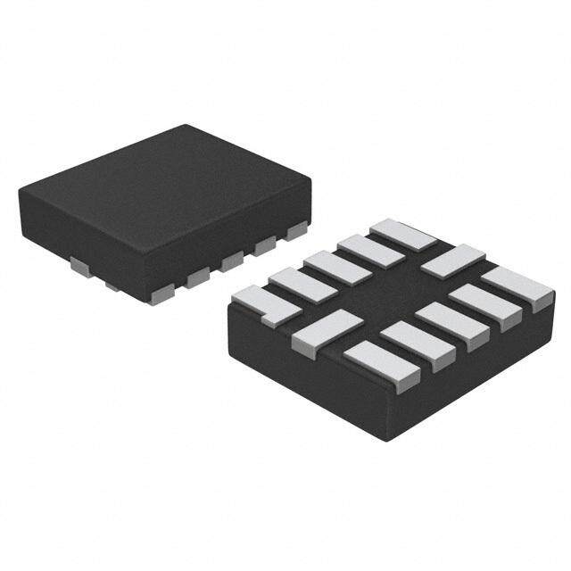
| 供应商器件封装 | 8-TSSOP |
| 其它名称 | 568-4243-2 |
| 包装 | 带卷 (TR) |
| 商标 | NXP Semiconductors |
| 安装类型 | 表面贴装 |
| 安装风格 | SMD/SMT |
| 封装 | Reel |
| 封装/外壳 | 8-TSSOP,8-MSOP(0.118",3.00mm 宽) |
| 封装/箱体 | TSSOP-8 |
| 工作温度 | -40°C ~ 85°C |
| 工厂包装数量 | 3000 |
| 差分-输入:输出 | 无/无 |
| 数据速率 | - |
| 最大工作温度 | + 85 C |
| 最小工作温度 | - 40 C |
| 标准包装 | 3,000 |
| 特色产品 | http://www.digikey.com/cn/zh/ph/NXP/I2C.html |
| 电压-电源 | 1 V ~ 3.6 V,1.8 V ~ 5.5 V |
| 电源电压-最大 | 5 V |
| 电源电压-最小 | 0 V |
| 输入类型 | 电压 |
| 输出/通道数 | 1 |
| 输出类型 | 电压 |
| 通道数 | 2 |
| 逻辑功能 | 变换器,双向,开路漏极 |
| 零件号别名 | PCA9306DP1-G |


- 商务部:美国ITC正式对集成电路等产品启动337调查
- 曝三星4nm工艺存在良率问题 高通将骁龙8 Gen1或转产台积电
- 太阳诱电将投资9.5亿元在常州建新厂生产MLCC 预计2023年完工
- 英特尔发布欧洲新工厂建设计划 深化IDM 2.0 战略
- 台积电先进制程称霸业界 有大客户加持明年业绩稳了
- 达到5530亿美元!SIA预计今年全球半导体销售额将创下新高
- 英特尔拟将自动驾驶子公司Mobileye上市 估值或超500亿美元
- 三星加码芯片和SET,合并消费电子和移动部门,撤换高东真等 CEO
- 三星电子宣布重大人事变动 还合并消费电子和移动部门
- 海关总署:前11个月进口集成电路产品价值2.52万亿元 增长14.8%


PDF Datasheet 数据手册内容提取
PCA9306 Dual bidirectional I2C-bus and SMBus voltage-level translator Rev. 8 — 22 January 2014 Product data sheet 1. General description The PCA9306 is a dual bidirectional I2C-bus and SMBus voltage-level translator with an enable (EN) input, and is operational from 1.0V to 3.6V (V ) and 1.8V to 5.5V ref(1) (V ). bias(ref)(2) The PCA9306 allows bidirectional voltage translations between 1.0V and 5V without the use of a direction pin. The low ON-state resistance (R ) of the switch allows connections on to be made with minimal propagation delay. When EN is HIGH, the translator switch is on, and the SCL1 and SDA1 I/O are connected to the SCL2 and SDA2 I/O, respectively, allowing bidirectional data flow between ports. When EN is LOW, the translator switch is off, and a high-impedance state exists between ports. The PCA9306 is not a bus buffer like the PCA9509 or PCA9517A that provide both level translation and physically isolates the capacitance to either side of the bus when both sides are connected. The PCA9306 only isolates both sides when the device is disabled and provides voltage level translation when active. The PCA9306 can also be used to run two buses, one at 400kHz operating frequency and the other at 100kHz operating frequency. If the two buses are operating at different frequencies, the 100kHz bus must be isolated when the 400kHz operation of the other bus is required. If the master is running at 400kHz, the maximum system operating frequency may be less than 400kHz because of the delays added by the translator. As with the standard I2C-bus system, pull-up resistors are required to provide the logic HIGH levels on the translator’s bus. The PCA9306 has a standard open-collector configuration of the I2C-bus. The size of these pull-up resistors depends on the system, but each side of the translator must have a pull-up resistor. The device is designed to work with Standard-mode, Fast-mode and Fast-mode Plus I2C-bus devices in addition to SMBus devices. The maximum frequency is dependent on the RC time constant, but generally supports >2MHz. When the SDA1 or SDA2 port is LOW, the clamp is in the ON-state and a low resistance connection exists between the SDA1 and SDA2 ports. Assuming the higher voltage is on the SDA2 port when the SDA2 port is HIGH, the voltage on the SDA1 port is limited to the voltage set by VREF1. When the SDA1 port is HIGH, the SDA2 port is pulled to the drain pull-up supply voltage (V ) by the pull-up resistors. This functionality allows a pu(D) seamless translation between higher and lower voltages selected by the user without the need for directional control. The SCL1/SCL2 channel also functions as the SDA1/SDA2 channel.
PCA9306 NXP Semiconductors Dual bidirectional I2C-bus and SMBus voltage-level translator All channels have the same electrical characteristics and there is minimal deviation from one output to another in voltage or propagation delay. This is a benefit over discrete transistor voltage translation solutions, since the fabrication of the switch is symmetrical. The translator provides excellent ESD protection to lower voltage devices, and at the same time protects less ESD-resistant devices. 2. Features and benefits 2-bit bidirectional translator for SDA and SCL lines in mixed-mode I2C-bus applications Standard-mode, Fast-mode, and Fast-mode Plus I2C-bus and SMBus compatible Less than 1.5ns maximum propagation delay to accommodate Standard-mode and Fast-mode I2C-bus devices and multiple masters Allows voltage level translation between: 1.0V V and 1.8V, 2.5V, 3.3V or 5V V ref(1) bias(ref)(2) 1.2V V and 1.8V, 2.5V, 3.3V or 5V V ref(1) bias(ref)(2) 1.8V V and 3.3V or 5V V ref(1) bias(ref)(2) 2.5V V and 5V V ref(1) bias(ref)(2) 3.3V V and 5V V ref(1) bias(ref)(2) Provides bidirectional voltage translation with no direction pin Low 3.5 ON-state connection between input and output ports provides less signal distortion Open-drain I2C-bus I/O ports (SCL1, SDA1, SCL2 and SDA2) 5V tolerant I2C-bus I/O ports to support mixed-mode signal operation High-impedance SCL1, SDA1, SCL2 and SDA2 pins for EN=LOW Lock-up free operation Flow through pinout for ease of printed-circuit board trace routing ESD protection exceeds 2000V HBM per JESD22-A114 and 1000V CDM per JESD22-C101 Packages offered: SO8, TSSOP8, VSSOP8, XQFN8, XSON8, XSON8U PCA9306 All information provided in this document is subject to legal disclaimers. © NXP B.V. 2014. All rights reserved. Product data sheet Rev. 8 — 22 January 2014 2 of 35
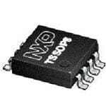
PCA9306 NXP Semiconductors Dual bidirectional I2C-bus and SMBus voltage-level translator 3. Ordering information Table 1. Ordering info rmation T =40C to +85C. amb Type number Topside Package mark Name Description Version PCA9306D PCA9306 SO8 plastic small outline package; 8leads; bodywidth3.9mm SOT96-1 PCA9306DC 306C VSSOP8 plastic very thin shrink small outline package; 8leads; SOT765-1 bodywidth2.3mm PCA9306DC1[1] P06 VSSOP8 plastic very thin shrink small outline package; 8leads; SOT765-1 bodywidth2.3mm PCA9306DC1/DG[2] P06 VSSOP8 plastic very thin shrink small outline package; 8leads; SOT765-1 bodywidth2.3mm PCA9306DP 306P TSSOP8[3] plastic thin shrink small outline package; 8 leads; SOT505-1 bodywidth3mm PCA9306DP1[4] 306T TSSOP8 plastic thin shrink small outline package; 8 leads; SOT505-2 bodywidth3mm; leadlength 0.5mm PCA9306GD1[5] P06 XSON8U plastic extremely thin small outline package; noleads; SOT996-2 8terminals; UTLPbased; body320.5mm PCA9306GF 06 XSON8 extremely thin small outline package; no leads; 8terminals; SOT1089 body 1.3510.5mm PCA9306GM P6X[6] XQFN8 plastic extremely thin quad flat package; no leads; SOT902-2 8terminals;body 1.61.60.5mm [1] Same footprint and pinout as the Texas Instruments PCA9306DCU. [2] PCA9306DC1/DG is functionally the same (electrically and mechanically) as the PCA9306DC1 and the Texas Instruments PCA9306DCT. It is produced in Dark Green (lead-free and halogen/antimony-free) package material, with a unique orderable part number for customers who desire to order and only receive Dark Green package material. [3] Also known as MSOP8. [4] Same footprint and pinout as the Texas Instruments PCA9306DCT. [5] Low cost, thinner, drop-in replacement for VSSOP8 (SOT765-1) package. [6] ‘X’ will change based on date code. 3.1 Ordering options Table 2. Ordering opt ions Type number Orderable Package Packing method Minimum Temperature partnumber order quantity PCA9306D PCA9306D,112 SO8 Standard marking * 2000 T =40Cto+85C amb IC’stube - DSC bulk pack PCA9306D,118 SO8 Reel 13” Q1/T1 2500 T =40Cto+85C amb *standardmark SMD PCA9306DC PCA9306DC,125 VSSOP8 Reel 7” Q3/T4 3000 T =40Cto+85C amb *standardmark PCA9306DC1 PCA9306DC1,125 VSSOP8 Reel 7” Q3/T4 3000 T =40Cto+85C amb *standardmark PCA9306DC1/DG PCA9306DC1/DG,125 VSSOP8 Reel 7” Q3/T4 3000 T =40Cto+85C amb *standardmark PCA9306 All information provided in this document is subject to legal disclaimers. © NXP B.V. 2014. All rights reserved. Product data sheet Rev. 8 — 22 January 2014 3 of 35
PCA9306 NXP Semiconductors Dual bidirectional I2C-bus and SMBus voltage-level translator Table 2. Ordering options …continued Type number Orderable Package Packing method Minimum Temperature partnumber order quantity PCA9306DP PCA9306DP,118 TSSOP8 Reel 13” Q1/T1 2500 T =40Cto+85C amb *standardmark SMD PCA9306DP1 PCA9306DP1,125 TSSOP8 Reel 7” Q3/T4 3000 T =40Cto+85C amb *standardmark PCA9306GD1 PCA9306GD1,125 XSON8U Reel 7” Q3/T4 3000 T =40Cto+85C amb *standardmark PCA9306GF PCA9306GF,115 XSON8 Reel 7” Q1/T1 5000 T =40Cto+85C amb *standardmark SMD PCA9306GM PCA9306GM,125 XQFN8 Reel 7” Q3/T4 4000 T =40Cto+85C amb *standardmark 4. Functional diagram VREF1 VREF2 2 7 PCA9306 8 EN 3 6 SCL1 SW SCL2 4 5 SDA1 SW SDA2 1 GND 002aab844 Fig 1. Logic diagram of PCA9306 (positive logic) PCA9306 All information provided in this document is subject to legal disclaimers. © NXP B.V. 2014. All rights reserved. Product data sheet Rev. 8 — 22 January 2014 4 of 35
PCA9306 NXP Semiconductors Dual bidirectional I2C-bus and SMBus voltage-level translator 5. Pinning information 5.1 Pinning GND 1 8 EN GND 1 8 EN VREF1 2 7 VREF2 VREF1 2 7 VREF2 PCA9306DP1 PCA9306DP SCL1 3 6 SCL2 SCL1 3 6 SCL2 SDA1 4 5 SDA2 SDA1 4 5 SDA2 002aab842 002aac373 Fig 2. Pin configuration for TSSOP8 Fig 3. Pin configuration for TSSOP8 (DP) (DP1) (MSOP8) PCA9306DC1 PCA9306DC1/DG VREF1 1 8 EN GND 1 8 EN SCL1 2 7 VREF2 VREF1 2 7 VREF2 PCA9306DC SDA1 3 6 SCL2 SCL1 3 6 SCL2 GND 4 5 SDA2 SDA1 4 5 SDA2 002aac374 002aab843 Fig 4. Pin configuration for VSSOP8 (DC) Fig 5. Pin configuration for VSSOP8 (DC1; DC1/DG) terminal 1 N index area E GND 1 8 7 VREF2 PCA9306GM VREF1 2 6 SCL2 GND 1 8 EN SCL1 3 5 SDA2 VREF1 2 7 VREF2 4 PCA9306D SCL1 3 6 SCL2 1 A SDA1 4 5 SDA2 SD 002aac375 002aac372 Transparent top view Fig 6. Pin configuration for SO8 Fig 7. Pin configuration for XQFN8 PCA9306 All information provided in this document is subject to legal disclaimers. © NXP B.V. 2014. All rights reserved. Product data sheet Rev. 8 — 22 January 2014 5 of 35
PCA9306 NXP Semiconductors Dual bidirectional I2C-bus and SMBus voltage-level translator GND 1 8 EN GND 1 8 EN VREF1 2 7 VREF2 VREF1 2 7 VREF2 PCA9306GD1 PCA9306GF SCL1 3 6 SCL2 SCL1 3 6 SCL2 SDA1 4 5 SDA2 SDA1 4 5 SDA2 002aae014 002aaf393 Transparent top view Transparent top view Fig 8. Pin configuration for XSON8U Fig 9. Pin configuration for XSON8 (GD1) 5.2 Pin description Table 3. Pin description Symbol Pin Description SO8, VSSOP8(DC) TSSOP8(MSOP8), TSSOP8, VSSOP8(DC1), XQFN8, XSON8, XSON8U(GD1) GND 1 4 ground (0V) VREF1 2 1 low-voltage side reference supply voltage for SCL1 and SDA1 SCL1 3 2 serial clock, low-voltage side; connect to VREF1 through a pull-up resistor SDA1 4 3 serial data, low-voltage side; connect to VREF1 through a pull-up resistor SDA2 5 5 serial data, high-voltage side; connect to VREF2 through a pull-up resistor SCL2 6 6 serial clock, high-voltage side; connect to VREF2 through a pull-up resistor VREF2 7 7 high-voltage side reference supply voltage for SCL2 and SDA2 EN 8 8 switch enable input; connect to VREF2 and pull-up through a high resistor PCA9306 All information provided in this document is subject to legal disclaimers. © NXP B.V. 2014. All rights reserved. Product data sheet Rev. 8 — 22 January 2014 6 of 35
PCA9306 NXP Semiconductors Dual bidirectional I2C-bus and SMBus voltage-level translator 6. Functional description Refer to Figure 1 “Logic diagram of PCA9306 (positive logic)”. 6.1 Function table Table 4. Function selection (example) H=HIGH level; L=LOW level. Input EN[1] Function H SCL1=SCL2; SDA1=SDA2 L disconnect [1] EN is controlled by the V logic levels and should be at least 1V higher than V for best bias(ref)(2) ref(1) translator operation. 7. Limiting values Table 5. Limiting values In accordance with the Absolute Maximum Rating System (IEC 60134). Over operating free-air temperature range. Symbol Parameter Conditions Min Max Unit V reference voltage (1) 0.5 +6 V ref(1) V reference bias voltage (2) 0.5 +6 V bias(ref)(2) V input voltage 0.5[1] +6 V I V voltage on an input/output pin 0.5[1] +6 V I/O I channel current (DC) - 128 mA ch I input clamping current V <0V - 50 mA IK I T storage temperature 65 +150 C stg [1] The input and input/output negative voltage ratings may be exceeded if the input and input/output clamp current ratings are observed. 8. Recommended operating conditions Table 6. Operating conditions Symbol Parameter Conditions Min Max Unit V voltage on an input/output pin SCL1,SDA1, 0 5 V I/O SCL2, SDA2 V [1] reference voltage (1) VREF1 0 5 V ref(1) V [1] reference bias voltage (2) VREF2 0 5 V bias(ref)(2) V input voltage on pin EN 0 5 V I(EN) I pass switch current - 64 mA sw(pass) T ambient temperature operating in free-air 40 +85 C amb [1] Vref(1)Vbias(ref)(2)1V for best results in level shifting applications. PCA9306 All information provided in this document is subject to legal disclaimers. © NXP B.V. 2014. All rights reserved. Product data sheet Rev. 8 — 22 January 2014 7 of 35
PCA9306 NXP Semiconductors Dual bidirectional I2C-bus and SMBus voltage-level translator 9. Static characteristics Table 7. Static charac teristics T =40C to +85C, unless otherwise specified. amb Symbol Parameter Conditions Min Typ[1] Max Unit V input clamping voltage I =18mA; V =0V - - 1.2 V IK I I(EN) I HIGH-level input current V =5V; V =0V - - 5 A IH I I(EN) C input capacitance on pin EN V =3V or 0V - 7.1 - pF i(EN) I C off-state input/output capacitance SCLn, SDAn; - 4 6 pF io(off) V =3Vor0V; V =0V O I(EN) C on-state input/output capacitance SCLn, SDAn; - 9.3 12.5 pF io(on) V =3Vor0V; V =3V O I(EN) R ON-state resistance[2] SCLn,SDAn; [3] on V =0V;I =64mA I O V =4.5V - 2.4 5.0 I(EN) V =3V - 3.0 6.0 I(EN) V =2.3V - 3.8 8.0 I(EN) V =1.5V - 15 32 I(EN) V =1.5V [4] - 32 80 I(EN) V =2.4V; I =15mA I O V =4.5V - 4.8 7.5 I(EN) V =3V - 46 80 I(EN) V =1.7V; I =15mA I O V =2.3V - 40 80 I(EN) [1] All typical values are at Tamb=25C. [2] Measured by the voltage drop between the SCL1 and SCL2, or SDA1 and SDA2 terminals at the indicated current through the switch. ON-state resistance is determined by the lowest voltage of the two terminals. [3] Guaranteed by design. [4] For DC, DC1 (VSSOP8) and GD1 (XSON8U) packages only. PCA9306 All information provided in this document is subject to legal disclaimers. © NXP B.V. 2014. All rights reserved. Product data sheet Rev. 8 — 22 January 2014 8 of 35
PCA9306 NXP Semiconductors Dual bidirectional I2C-bus and SMBus voltage-level translator 10. Dynamic characteristics Table 8. Dynamic cha racteristics (translating down) T =40C to +85C, unless otherwise specified. Values guaranteed by design. amb Symbol Parameter Conditions C =50pF C =30pF C =15pF Unit L L L Min Max Min Max Min Max V =3.3V; V =3.3V; V =0V; V =1.15V (see Figure10) I(EN) IH IL M t LOWtoHIGH from (input) SCL2 or SDA2 0 2.0 0 1.2 0 0.6 ns PLH propagation delay to (output) SCL1 or SDA1 t HIGHtoLOW from (input) SCL2 or SDA2 0 2.0 0 1.5 0 0.75 ns PHL propagation delay to (output) SCL1 or SDA1 V =2.5V; V =2.5V; V =0V; V =0.75V (see Figure10) I(EN) IH IL M t LOWtoHIGH from (input) SCL2 or SDA2 0 2.0 0 1.2 0 0.6 ns PLH propagation delay to (output) SCL1 or SDA1 t HIGHtoLOW from (input) SCL2 or SDA2 0 2.5 0 1.5 0 0.75 ns PHL propagation delay to (output) SCL1 or SDA1 Table 9. Dynamic cha racteristics (translating up) T =40C to +85C, unless otherwise specified. Values guaranteed by design. amb Symbol Parameter Conditions C =50pF C =30pF C =15pF Unit L L L Min Max Min Max Min Max V =3.3V; V =2.3V; V =0V; V =3.3V; V =1.15V; R =300 (see Figure10) I(EN) IH IL TT M L t LOWtoHIGH from (input) SCL1 or SDA1 0 1.75 0 1.0 0 0.5 ns PLH propagation delay to (output) SCL2 or SDA2 t HIGHtoLOW from (input) SCL1 or SDA1 0 2.75 0 1.65 0 0.8 ns PHL propagation delay to (output) SCL2 or SDA2 V =2.5V; V =1.5V; V =0V; V =2.5V; V =0.75V; R =300 (see Figure10) I(EN) IH IL TT M L t LOWtoHIGH from (input) SCL1 or SDA1 0 1.75 0 1.0 0 0.5 ns PLH propagation delay to (output) SCL2 or SDA2 t HIGHtoLOW from (input) SCL1 or SDA1 0 3.3 0 2.0 0 1.0 ns PHL propagation delay to (output) SCL2 or SDA2 VIH VTT input VM VM VIL RL S1 VOH from output under test S2 (open) output VM VM CL VOL 002aab845 002aab846 a. Load circuit b. Timing diagram S1=translating up; S2=translating down. CL includes probe and jig capacitance. All input pulses are supplied by generators having the following characteristics: PRR10MHz; Zo=50; tr2ns; tf2ns. The outputs are measured one at a time, with one transition per measurement. Fig 10. Load circuit for outputs PCA9306 All information provided in this document is subject to legal disclaimers. © NXP B.V. 2014. All rights reserved. Product data sheet Rev. 8 — 22 January 2014 9 of 35
PCA9306 NXP Semiconductors Dual bidirectional I2C-bus and SMBus voltage-level translator 11. Application information Vpu(D) = 3.3 V(1) 200 kΩ PCA9306 Vref(1) = 1.8 V(1) 8 EN RPU RPU VREF1 VREF2 2 7 RPU RPU VCC VCC SCL1 3 6 SCL2 SCL SW SCL I2C-BUS I2C-BUS MASTER DEVICE SDA1 4 5 SDA2 SDA SW SDA GND 1 GND GND 002aab847 (1) The applied voltages at V and V should be such that V is at least 1V higher than ref(1) pu(D) bias(ref)(2) Vref(1) for best translator operation. Fig 11. Typical application circuit (switch always enabled) 3.3 V enable signal(1) Vpu(D) = 3.3 V on off 200 kΩ PCA9306 Vref(1) = 1.8 V(1) 8 EN RPU RPU VREF1 VREF2 2 7 RPU RPU VCC VCC SCL1 3 6 SCL2 SCL SW SCL I2C-BUS I2C-BUS MASTER DEVICE SDA1 4 5 SDA2 SDA SW SDA GND 1 GND GND 002aab848 (1) In the Enabled mode, the applied enable voltage and the applied voltage at V should be such ref(1) that Vbias(ref)(2) is at least 1V higher than Vref(1) for best translator operation. Fig 12. Typical application circuit (switch enable control) PCA9306 All information provided in this document is subject to legal disclaimers. © NXP B.V. 2014. All rights reserved. Product data sheet Rev. 8 — 22 January 2014 10 of 35
PCA9306 NXP Semiconductors Dual bidirectional I2C-bus and SMBus voltage-level translator 11.1 Bidirectional translation For the bidirectional clamping configuration (higher voltage to lower voltage or lower voltage to higher voltage), the EN input must be connected to VREF2 and both pins pulled to HIGH side V through a pull-up resistor (typically 200k). This allows VREF2 to pu(D) regulate the EN input. A filter capacitor on VREF2 is recommended. The I2C-bus master output can be totempole or open-drain (pull-up resistors may be required) and the I2C-bus device output can be totempole or open-drain (pull-up resistors are required to pull the SCL2 and SDA2 outputs to V ). However, if either output is totempole, data pu(D) must be unidirectional or the outputs must be 3-stateable and be controlled by some direction-control mechanism to prevent HIGH-to-LOW contentions in either direction. If both outputs are open-drain, no direction control is needed. The reference supply voltage (V ) is connected to the processor core power supply ref(1) voltage. When VREF2 is connected through a 200k resistor to a 3.3V to 5.5V V pu(D) power supply, and V is set between 1.0V and (V 1V), the output of each SCL1 ref(1) pu(D) and SDA1 has a maximum output voltage equal to VREF1, and the output of each SCL2 and SDA2 has a maximum output voltage equal to V . pu(D) Table 10. Application operating conditions Refer to Figure11. Symbol Parameter Conditions Min Typ[1] Max Unit V reference bias voltage (2) V +0.6 2.1 5 V bias(ref)(2) ref(1) V input voltage on pin EN V +0.6 2.1 5 V I(EN) ref(1) V reference voltage (1) 0 1.5 4.4 V ref(1) I pass switch current - 14 - mA sw(pass) I reference current transistor - 5 - A ref T ambient temperature operating in 40 - +85 C amb free-air [1] All typical values are at Tamb=25C. 11.2 How to size pull-up resistor value Sizing the pull-up resistor on an open-drain bus is specific to the individual application and is dependent on the following driver characteristics: • The driver sink current • The V of driver OL • The V of the driver IL • Frequency of operation The following tables can be used to estimate the pull-up resistor value in different use cases so that the minimum resistance for the pull-up resistor can be found. Table11, Table12 and Table13 contain suggested minimum values of pull-up resistors for the PCA9306 and NVT20xx devices with typical voltage translation levels and drive currents. The calculated values assume that both drive currents are the same. V =V =0.1V and accounts for a 5%V tolerance of the supplies, 1% OL IL CC CC resistor values. It should be noted that the resistor chosen in the final application should be equal to or larger than the values shown in Table11, Table12 and Table13 to ensure that the pass voltage is less than 10% of the V voltage, and the external driver should CC PCA9306 All information provided in this document is subject to legal disclaimers. © NXP B.V. 2014. All rights reserved. Product data sheet Rev. 8 — 22 January 2014 11 of 35
PCA9306 NXP Semiconductors Dual bidirectional I2C-bus and SMBus voltage-level translator be able to sink the total current from both pull-up resistors. When selecting the minimum resistor value in Table11, Table12 or Table13, the drive current strength that should be chosen should be the lowest drive current seen in the application and account for any drive strength current scaling with output voltage. For the GTL devices, the resistance table should be recalculated to account for the difference in ON resistance and bias voltage limitations between V and V . CC(B) CC(A) Table 11. Pull-up resis tor minimum values, 3mA driver sink current for PCA9306 and NVT20xx A-side B-side 1.2V 1.5V 1.8V 2.5V 3.3V 5.0V 1.0V R =750 R =845 R =976 R =none R =none R =none pu(A) pu(A) pu(A) pu(A) pu(A) pu(A) R =750 R =845 R =976 R =887 R =1.18k R =1.82k pu(B) pu(B) pu(B) pu(B) pu(B) pu(B) 1.2V R =931 R =1.02k R =none R =none R =none pu(A) pu(A) pu(A) pu(A) pu(A) R =931 R =1.02k R =887 R =1.18k R =1.82k pu(B) pu(B) pu(B) pu(B) pu(B) 1.5V R =1.1k R =none R =none R =none pu(A) pu(A) pu(A) pu(A) R =1.1k R =866 R =1.18k R =1.78k pu(B) pu(B) pu(B) pu(B) 1.8V R =1.47k R =none R =none pu(A) pu(A) pu(A) R =1.47k R =1.15k R =1.78k pu(B) pu(B) pu(B) 2.5V R =1.96k R =none pu(A) pu(A) R =1.96k R =1.78k pu(B) pu(B) 3.3V R =none pu(A) R =1.74k pu(B) Table 12. Pull-up resis tor minimum values, 10mA driver sink current for PCA9306 and NVT20xx A-side B-side 1.2V 1.5V 1.8V 2.5V 3.3V 5.0V 1.0V R =221 R =255 R =287 R =none R =none R =none pu(A) pu(A) pu(A) pu(A) pu(A) pu(A) R =221 R =255 R =287 R =267 R =357 R =549 pu(B) pu(B) pu(B) pu(B) pu(B) pu(B) 1.2V R =274 R =309 R =none R =none R =none pu(A) pu(A) pu(A) pu(A) pu(A) R =274 R =309 R =267 R =357 R =549 pu(B) pu(B) pu(B) pu(B) pu(B) 1.5V R =332 R =none R =none R =none pu(A) pu(A) pu(A) pu(A) R =332 R =261 R =348 R =536 pu(B) pu(B) pu(B) pu(B) 1.8V R =442 R =none R =none pu(A) pu(A) pu(A) R =442 R =348 R =536 pu(B) pu(B) pu(B) 2.5V R =590 R =none pu(A) pu(A) R =590 R =523 pu(B) pu(B) 3.3V R =none pu(A) R =523 pu(B) PCA9306 All information provided in this document is subject to legal disclaimers. © NXP B.V. 2014. All rights reserved. Product data sheet Rev. 8 — 22 January 2014 12 of 35
PCA9306 NXP Semiconductors Dual bidirectional I2C-bus and SMBus voltage-level translator Table 13. Pull-up resis tor minimum values, 15mA driver sink current for PCA9306 and NVT20xx A-side B-side 1.2V 1.5V 1.8V 2.5V 3.3V 5.0V 1.0V R =147 R =169 R =191 R =none R =none R =none pu(A) pu(A) pu(A) pu(A) pu(A) pu(A) R =147 R =169 R =191 R =178 R =237 R =365 pu(B) pu(B) pu(B) pu(B) pu(B) pu(B) 1.2V R =182 R =205 R =none R =none R =none pu(A) pu(A) pu(A) pu(A) pu(A) R =182 R =205 R =178 R =237 R =365 pu(B) pu(B) pu(B) pu(B) pu(B) 1.5V R =221 R =none R =none R =none pu(A) pu(A) pu(A) pu(A) R =221 R =174 R =232 R =357 pu(B) pu(B) pu(B) pu(B) 1.8V R =294 R =none R =none pu(A) pu(A) pu(A) R =294 R =232 R =357 pu(B) pu(B) pu(B) 2.5V R =392 R =none pu(A) pu(A) R =392 R =357 pu(B) pu(B) 3.3V R =none pu(A) R =348 pu(B) 11.3 How to design for maximum frequency operation The maximum frequency is limited by the minimum pulse width LOW and HIGH as well as rise time and fall time. See Equation1 as an example of the maximum frequency. The rise and fall times are shown in Figure13. 1 f = ------------------------------------------------------------------------------------------------------------- (1) max t +t +t +t LOWmin HIGHmin ractual factual tr(actual) tf(actual) tHIGH(min) VIH VCC 0.9 × VCC tLOW(min) VIL VOL 1 / fmax 0.1 × VCC GND 002aag912 Fig 13. An example waveform for maximum frequency The rise and fall times are dependent upon translation voltages, the drive strength, the total node capacitance (C ) and the pull-up resistors (R ) that are present on the bus. L(tot) PU The node capacitance is the addition of the PCB trace capacitance and the device capacitance that exists on the bus. Because of the dependency of the external components, PCB layout and the different device operating states the calculation of rise and fall times is complex and has several inflection points along the curve. The main component of the rise and fall times is the RC time constant of the bus line when the device is in its two primary operating states: when device is in the ON state and it is low-impedance, the other is when the device is OFF isolating the A-side from the B-side. A description of the fall time applied to either An or Bn output going from HIGH to LOW is as follows. Whichever side is asserted first, the B-side down must discharge to the V CC(A) voltage. The time is determined by the pull-up resistor, pull-down driver strength and the PCA9306 All information provided in this document is subject to legal disclaimers. © NXP B.V. 2014. All rights reserved. Product data sheet Rev. 8 — 22 January 2014 13 of 35
PCA9306 NXP Semiconductors Dual bidirectional I2C-bus and SMBus voltage-level translator capacitance. As the level moves below the V voltage, the channel resistance drops CC(A) so that both A and B sides equal. The capacitance on both sides is connected to form the total capacitance and the pull-up resistors on both sides combine to the parallel equivalent resistance. The R of the device is small compared to the pull-up resistor values, so its on effect on the pull-up resistance can be neglected and the fall is determined by the driver pulling the combined capacitance and pull-up resistor currents. An estimation of the actual fall time seen by the device is equal to the time it takes for the B-side to fall to the V CC(A) voltage and the time it takes for both sides to fall from the V voltage to the V level. CC(A) IL A description of the rise time applied to either An or Bn output going from LOW to HIGH is as follows. When the signal level is LOW, the R is at its minimum, so the A and B sides on are essentially one node. They will rise together with an RC time constant that is the sum of all the capacitance from both sides and the parallel of the resistance from both sides. As the signal approaches the V voltage, the channel resistance goes up and the CC(A) waveforms separate, with the B side finishing its rise with the RC time constant of the Bside. The rise to V is essentially the same for both sides. CC(A) There are some basic guidelines to follow that will help maximize the performance of the device: • Keep trace length to a minimum by placing the NVT device close to the processor. • The signal round trip time on trace should be shorter than the rise or fall time of signal to reduce reflections. • The faster the edge of the signal, the higher the chance for ringing. • The higher drive strength controlled by the pull-up resistor (up to 15mA), the higher the frequency the device can use. The system designer must design the pull-up resistor value based on external current drive strength and limit the node capacitance (minimize the wire, stub, connector and trace length) to get the desired operation frequency result. PCA9306 All information provided in this document is subject to legal disclaimers. © NXP B.V. 2014. All rights reserved. Product data sheet Rev. 8 — 22 January 2014 14 of 35
PCA9306 NXP Semiconductors Dual bidirectional I2C-bus and SMBus voltage-level translator 12. Package outline (cid:54)(cid:50)(cid:27)(cid:29)(cid:3)(cid:83)(cid:79)(cid:68)(cid:86)(cid:87)(cid:76)(cid:70)(cid:3)(cid:86)(cid:80)(cid:68)(cid:79)(cid:79)(cid:3)(cid:82)(cid:88)(cid:87)(cid:79)(cid:76)(cid:81)(cid:72)(cid:3)(cid:83)(cid:68)(cid:70)(cid:78)(cid:68)(cid:74)(cid:72)(cid:30)(cid:3)(cid:27)(cid:3)(cid:79)(cid:72)(cid:68)(cid:71)(cid:86)(cid:30)(cid:3)(cid:69)(cid:82)(cid:71)(cid:92)(cid:3)(cid:90)(cid:76)(cid:71)(cid:87)(cid:75)(cid:3)(cid:22)(cid:17)(cid:28)(cid:3)(cid:80)(cid:80)(cid:3) (cid:54)(cid:50)(cid:55)(cid:28)(cid:25)(cid:16)(cid:20)(cid:3) (cid:39)(cid:3) (cid:40)(cid:3) (cid:36)(cid:3) (cid:59)(cid:3) (cid:70)(cid:3) (cid:92)(cid:3) (cid:43)(cid:3)(cid:40)(cid:3) (cid:89)(cid:3)(cid:48)(cid:3) (cid:36)(cid:3) (cid:61)(cid:3) (cid:27)(cid:3) (cid:24)(cid:3) (cid:52)(cid:3) (cid:36)(cid:3)(cid:21)(cid:3)(cid:36)(cid:3)(cid:20)(cid:3) (cid:11)(cid:36)(cid:3)(cid:22)(cid:3)(cid:3)(cid:12)(cid:3) (cid:36)(cid:3) (cid:83)(cid:76)(cid:81)(cid:3)(cid:20)(cid:3)(cid:76)(cid:81)(cid:71)(cid:72)(cid:91)(cid:3) (cid:537)(cid:3) (cid:47)(cid:3)(cid:83)(cid:3) (cid:20)(cid:3) (cid:23)(cid:3) (cid:47)(cid:3) (cid:72)(cid:3) (cid:90)(cid:3)(cid:48)(cid:3) (cid:71)(cid:72)(cid:87)(cid:68)(cid:76)(cid:79)(cid:3)(cid:59)(cid:3) (cid:69)(cid:3)(cid:83)(cid:3) (cid:19)(cid:3) (cid:21)(cid:17)(cid:24)(cid:3) (cid:24)(cid:3)(cid:80)(cid:80)(cid:3) (cid:86)(cid:70)(cid:68)(cid:79)(cid:72)(cid:3) (cid:39)(cid:44)(cid:48)(cid:40)(cid:49)(cid:54)(cid:44)(cid:50)(cid:49)(cid:54)(cid:3)(cid:11)(cid:76)(cid:81)(cid:70)(cid:75)(cid:3)(cid:71)(cid:76)(cid:80)(cid:72)(cid:81)(cid:86)(cid:76)(cid:82)(cid:81)(cid:86)(cid:3)(cid:68)(cid:85)(cid:72)(cid:3)(cid:71)(cid:72)(cid:85)(cid:76)(cid:89)(cid:72)(cid:71)(cid:3)(cid:73)(cid:85)(cid:82)(cid:80)(cid:3)(cid:87)(cid:75)(cid:72)(cid:3)(cid:82)(cid:85)(cid:76)(cid:74)(cid:76)(cid:81)(cid:68)(cid:79)(cid:3)(cid:80)(cid:80)(cid:3)(cid:71)(cid:76)(cid:80)(cid:72)(cid:81)(cid:86)(cid:76)(cid:82)(cid:81)(cid:86)(cid:12)(cid:3) (cid:56)(cid:49)(cid:44)(cid:55)(cid:3) (cid:80)(cid:36)(cid:68)(cid:91)(cid:3)(cid:17)(cid:3) (cid:36)(cid:3)(cid:20)(cid:3) (cid:36)(cid:3)(cid:21)(cid:3) (cid:36)(cid:3)(cid:22)(cid:3) (cid:69)(cid:3)(cid:83)(cid:3) (cid:70)(cid:3) (cid:39)(cid:3)(cid:11)(cid:20)(cid:12)(cid:3) (cid:40)(cid:3)(cid:11)(cid:21)(cid:12)(cid:3) (cid:72)(cid:3) (cid:43)(cid:3)(cid:40)(cid:3) (cid:47)(cid:3) (cid:47)(cid:3)(cid:83)(cid:3) (cid:52)(cid:3) (cid:89)(cid:3) (cid:90)(cid:3) (cid:92)(cid:3) (cid:61)(cid:3)(cid:11)(cid:20)(cid:12)(cid:3) (cid:537)(cid:3) (cid:19)(cid:17)(cid:21)(cid:24)(cid:3) (cid:20)(cid:17)(cid:23)(cid:24)(cid:3) (cid:19)(cid:17)(cid:23)(cid:28)(cid:3) (cid:19)(cid:17)(cid:21)(cid:24)(cid:3) (cid:24)(cid:17)(cid:19)(cid:3) (cid:23)(cid:17)(cid:19)(cid:3) (cid:25)(cid:17)(cid:21)(cid:3) (cid:20)(cid:17)(cid:19)(cid:3) (cid:19)(cid:17)(cid:26)(cid:3) (cid:19)(cid:17)(cid:26)(cid:3) (cid:80)(cid:80)(cid:3) (cid:20)(cid:17)(cid:26)(cid:24)(cid:3) (cid:19)(cid:17)(cid:21)(cid:24)(cid:3) (cid:20)(cid:17)(cid:21)(cid:26)(cid:3) (cid:20)(cid:17)(cid:19)(cid:24)(cid:3) (cid:19)(cid:17)(cid:21)(cid:24)(cid:3) (cid:19)(cid:17)(cid:21)(cid:24)(cid:3) (cid:19)(cid:17)(cid:20)(cid:3) (cid:19)(cid:17)(cid:20)(cid:19)(cid:3) (cid:20)(cid:17)(cid:21)(cid:24)(cid:3) (cid:19)(cid:17)(cid:22)(cid:25)(cid:3) (cid:19)(cid:17)(cid:20)(cid:28)(cid:3) (cid:23)(cid:17)(cid:27)(cid:3) (cid:22)(cid:17)(cid:27)(cid:3) (cid:24)(cid:17)(cid:27)(cid:3) (cid:19)(cid:17)(cid:23)(cid:3) (cid:19)(cid:17)(cid:25)(cid:3) (cid:19)(cid:17)(cid:22)(cid:3) (cid:27)(cid:3)(cid:82)(cid:3) (cid:19)(cid:17)(cid:19)(cid:20)(cid:19)(cid:3) (cid:19)(cid:17)(cid:19)(cid:24)(cid:26)(cid:3) (cid:19)(cid:17)(cid:19)(cid:20)(cid:28)(cid:3)(cid:19)(cid:17)(cid:19)(cid:20)(cid:19)(cid:19)(cid:3) (cid:19)(cid:17)(cid:21)(cid:19)(cid:3) (cid:19)(cid:17)(cid:20)(cid:25)(cid:3) (cid:19)(cid:17)(cid:21)(cid:23)(cid:23)(cid:3) (cid:19)(cid:17)(cid:19)(cid:22)(cid:28)(cid:3) (cid:19)(cid:17)(cid:19)(cid:21)(cid:27)(cid:3) (cid:19)(cid:17)(cid:19)(cid:21)(cid:27)(cid:3) (cid:19)(cid:3)(cid:82)(cid:3) (cid:76)(cid:81)(cid:70)(cid:75)(cid:72)(cid:86)(cid:3) (cid:19)(cid:17)(cid:19)(cid:25)(cid:28)(cid:3) (cid:19)(cid:17)(cid:19)(cid:20)(cid:3) (cid:19)(cid:17)(cid:19)(cid:24)(cid:3) (cid:19)(cid:17)(cid:19)(cid:23)(cid:20)(cid:3) (cid:19)(cid:17)(cid:19)(cid:20)(cid:3) (cid:19)(cid:17)(cid:19)(cid:20)(cid:3) (cid:19)(cid:17)(cid:19)(cid:19)(cid:23)(cid:3) (cid:19)(cid:17)(cid:19)(cid:19)(cid:23)(cid:3) (cid:19)(cid:17)(cid:19)(cid:23)(cid:28)(cid:3) (cid:19)(cid:17)(cid:19)(cid:20)(cid:23)(cid:3)(cid:19)(cid:17)(cid:19)(cid:19)(cid:26)(cid:24)(cid:3) (cid:19)(cid:17)(cid:20)(cid:28)(cid:3) (cid:19)(cid:17)(cid:20)(cid:24)(cid:3) (cid:19)(cid:17)(cid:21)(cid:21)(cid:27)(cid:3) (cid:19)(cid:17)(cid:19)(cid:20)(cid:25)(cid:3) (cid:19)(cid:17)(cid:19)(cid:21)(cid:23)(cid:3) (cid:19)(cid:17)(cid:19)(cid:20)(cid:21)(cid:3) (cid:49)(cid:82)(cid:87)(cid:72)(cid:86)(cid:3) (cid:20)(cid:17)(cid:3)(cid:51)(cid:79)(cid:68)(cid:86)(cid:87)(cid:76)(cid:70)(cid:3)(cid:82)(cid:85)(cid:3)(cid:80)(cid:72)(cid:87)(cid:68)(cid:79)(cid:3)(cid:83)(cid:85)(cid:82)(cid:87)(cid:85)(cid:88)(cid:86)(cid:76)(cid:82)(cid:81)(cid:86)(cid:3)(cid:82)(cid:73)(cid:3)(cid:19)(cid:17)(cid:20)(cid:24)(cid:3)(cid:80)(cid:80)(cid:3)(cid:11)(cid:19)(cid:17)(cid:19)(cid:19)(cid:25)(cid:3)(cid:76)(cid:81)(cid:70)(cid:75)(cid:12)(cid:3)(cid:80)(cid:68)(cid:91)(cid:76)(cid:80)(cid:88)(cid:80)(cid:3)(cid:83)(cid:72)(cid:85)(cid:3)(cid:86)(cid:76)(cid:71)(cid:72)(cid:3)(cid:68)(cid:85)(cid:72)(cid:3)(cid:81)(cid:82)(cid:87)(cid:3)(cid:76)(cid:81)(cid:70)(cid:79)(cid:88)(cid:71)(cid:72)(cid:71)(cid:17)(cid:3) (cid:21)(cid:17)(cid:3)(cid:51)(cid:79)(cid:68)(cid:86)(cid:87)(cid:76)(cid:70)(cid:3)(cid:82)(cid:85)(cid:3)(cid:80)(cid:72)(cid:87)(cid:68)(cid:79)(cid:3)(cid:83)(cid:85)(cid:82)(cid:87)(cid:85)(cid:88)(cid:86)(cid:76)(cid:82)(cid:81)(cid:86)(cid:3)(cid:82)(cid:73)(cid:3)(cid:19)(cid:17)(cid:21)(cid:24)(cid:3)(cid:80)(cid:80)(cid:3)(cid:11)(cid:19)(cid:17)(cid:19)(cid:20)(cid:3)(cid:76)(cid:81)(cid:70)(cid:75)(cid:12)(cid:3)(cid:80)(cid:68)(cid:91)(cid:76)(cid:80)(cid:88)(cid:80)(cid:3)(cid:83)(cid:72)(cid:85)(cid:3)(cid:86)(cid:76)(cid:71)(cid:72)(cid:3)(cid:68)(cid:85)(cid:72)(cid:3)(cid:81)(cid:82)(cid:87)(cid:3)(cid:76)(cid:81)(cid:70)(cid:79)(cid:88)(cid:71)(cid:72)(cid:71)(cid:17)(cid:3)(cid:3) (cid:50)(cid:56)(cid:55)(cid:47)(cid:44)(cid:49)(cid:40)(cid:3) (cid:3)(cid:53)(cid:40)(cid:41)(cid:40)(cid:53)(cid:40)(cid:49)(cid:38)(cid:40)(cid:54)(cid:3) (cid:40)(cid:56)(cid:53)(cid:50)(cid:51)(cid:40)(cid:36)(cid:49)(cid:3) (cid:44)(cid:54)(cid:54)(cid:56)(cid:40)(cid:3)(cid:39)(cid:36)(cid:55)(cid:40)(cid:3) (cid:57)(cid:40)(cid:53)(cid:54)(cid:44)(cid:50)(cid:49)(cid:3) (cid:3)(cid:44)(cid:40)(cid:38)(cid:3) (cid:3)(cid:45)(cid:40)(cid:39)(cid:40)(cid:38)(cid:3) (cid:3)(cid:45)(cid:40)(cid:44)(cid:55)(cid:36)(cid:3) (cid:51)(cid:53)(cid:50)(cid:45)(cid:40)(cid:38)(cid:55)(cid:44)(cid:50)(cid:49)(cid:3) (cid:28)(cid:28)(cid:16)(cid:20)(cid:21)(cid:16)(cid:21)(cid:26)(cid:3) (cid:3)(cid:54)(cid:50)(cid:55)(cid:28)(cid:25)(cid:16)(cid:20)(cid:3) (cid:19)(cid:26)(cid:25)(cid:40)(cid:19)(cid:22)(cid:3) (cid:3)(cid:48)(cid:54)(cid:16)(cid:19)(cid:20)(cid:21)(cid:3) (cid:19)(cid:22)(cid:16)(cid:19)(cid:21)(cid:16)(cid:20)(cid:27)(cid:3) Fig 14. Package outline SOT96-1 (SO8) PCA9306 All information provided in this document is subject to legal disclaimers. © NXP B.V. 2014. All rights reserved. Product data sheet Rev. 8 — 22 January 2014 15 of 35
PCA9306 NXP Semiconductors Dual bidirectional I2C-bus and SMBus voltage-level translator (cid:55)(cid:54)(cid:54)(cid:50)(cid:51)(cid:27)(cid:29)(cid:3)(cid:83)(cid:79)(cid:68)(cid:86)(cid:87)(cid:76)(cid:70)(cid:3)(cid:87)(cid:75)(cid:76)(cid:81)(cid:3)(cid:86)(cid:75)(cid:85)(cid:76)(cid:81)(cid:78)(cid:3)(cid:86)(cid:80)(cid:68)(cid:79)(cid:79)(cid:3)(cid:82)(cid:88)(cid:87)(cid:79)(cid:76)(cid:81)(cid:72)(cid:3)(cid:83)(cid:68)(cid:70)(cid:78)(cid:68)(cid:74)(cid:72)(cid:30)(cid:3)(cid:27)(cid:3)(cid:79)(cid:72)(cid:68)(cid:71)(cid:86)(cid:30)(cid:3)(cid:69)(cid:82)(cid:71)(cid:92)(cid:3)(cid:90)(cid:76)(cid:71)(cid:87)(cid:75)(cid:3)(cid:22)(cid:3)(cid:80)(cid:80)(cid:3) (cid:54)(cid:50)(cid:55)(cid:24)(cid:19)(cid:24)(cid:16)(cid:20)(cid:3) (cid:39)(cid:3) (cid:40)(cid:3) (cid:36)(cid:3) (cid:59)(cid:3) (cid:70)(cid:3) (cid:92)(cid:3) (cid:43)(cid:40)(cid:3) (cid:89)(cid:3)(cid:48)(cid:3) (cid:36)(cid:3) (cid:61)(cid:3) (cid:27)(cid:3) (cid:24)(cid:3) (cid:36)(cid:21)(cid:3)(cid:36)(cid:20)(cid:3) (cid:11)(cid:36)(cid:22)(cid:12)(cid:3) (cid:36)(cid:3) (cid:83)(cid:76)(cid:81)(cid:3)(cid:20)(cid:3)(cid:76)(cid:81)(cid:71)(cid:72)(cid:91)(cid:3) (cid:537)(cid:3) (cid:47)(cid:83)(cid:3) (cid:47)(cid:3) (cid:20)(cid:3) (cid:23)(cid:3) (cid:71)(cid:72)(cid:87)(cid:68)(cid:76)(cid:79)(cid:3)(cid:59)(cid:3) (cid:72)(cid:3) (cid:90)(cid:3)(cid:48)(cid:3) (cid:69)(cid:83)(cid:3) (cid:19)(cid:3) (cid:21)(cid:17)(cid:24)(cid:3) (cid:24)(cid:3)(cid:80)(cid:80)(cid:3) (cid:86)(cid:70)(cid:68)(cid:79)(cid:72)(cid:3) (cid:39)(cid:44)(cid:48)(cid:40)(cid:49)(cid:54)(cid:44)(cid:50)(cid:49)(cid:54)(cid:3)(cid:11)(cid:80)(cid:80)(cid:3)(cid:68)(cid:85)(cid:72)(cid:3)(cid:87)(cid:75)(cid:72)(cid:3)(cid:82)(cid:85)(cid:76)(cid:74)(cid:76)(cid:81)(cid:68)(cid:79)(cid:3)(cid:71)(cid:76)(cid:80)(cid:72)(cid:81)(cid:86)(cid:76)(cid:82)(cid:81)(cid:86)(cid:12)(cid:3) (cid:56)(cid:49)(cid:44)(cid:55)(cid:3) (cid:80)(cid:36)(cid:68)(cid:91)(cid:3)(cid:17)(cid:3) (cid:36)(cid:20)(cid:3) (cid:36)(cid:21)(cid:3) (cid:36)(cid:22)(cid:3) (cid:69)(cid:83)(cid:3) (cid:70)(cid:3) (cid:39)(cid:11)(cid:20)(cid:12)(cid:3) (cid:40)(cid:11)(cid:21)(cid:12)(cid:3) (cid:72)(cid:3) (cid:43)(cid:40)(cid:3) (cid:47)(cid:3) (cid:47)(cid:83)(cid:3) (cid:89)(cid:3) (cid:90)(cid:3) (cid:92)(cid:3) (cid:61)(cid:11)(cid:20)(cid:12)(cid:3) (cid:537)(cid:3) (cid:19)(cid:17)(cid:20)(cid:24)(cid:3) (cid:19)(cid:17)(cid:28)(cid:24)(cid:3) (cid:19)(cid:17)(cid:23)(cid:24)(cid:3) (cid:19)(cid:17)(cid:21)(cid:27)(cid:3) (cid:22)(cid:17)(cid:20)(cid:3) (cid:22)(cid:17)(cid:20)(cid:3) (cid:24)(cid:17)(cid:20)(cid:3) (cid:19)(cid:17)(cid:26)(cid:3) (cid:19)(cid:17)(cid:26)(cid:19)(cid:3) (cid:25)(cid:131)(cid:3) (cid:80)(cid:80)(cid:3) (cid:20)(cid:17)(cid:20)(cid:3) (cid:19)(cid:17)(cid:21)(cid:24)(cid:3) (cid:19)(cid:17)(cid:25)(cid:24)(cid:3) (cid:19)(cid:17)(cid:28)(cid:23)(cid:3) (cid:19)(cid:17)(cid:20)(cid:3) (cid:19)(cid:17)(cid:20)(cid:3) (cid:19)(cid:17)(cid:20)(cid:3) (cid:19)(cid:17)(cid:19)(cid:24)(cid:3) (cid:19)(cid:17)(cid:27)(cid:19)(cid:3) (cid:19)(cid:17)(cid:21)(cid:24)(cid:3) (cid:19)(cid:17)(cid:20)(cid:24)(cid:3) (cid:21)(cid:17)(cid:28)(cid:3) (cid:21)(cid:17)(cid:28)(cid:3) (cid:23)(cid:17)(cid:26)(cid:3) (cid:19)(cid:17)(cid:23)(cid:3) (cid:19)(cid:17)(cid:22)(cid:24)(cid:3) (cid:19)(cid:131)(cid:3) (cid:49)(cid:82)(cid:87)(cid:72)(cid:86)(cid:3) (cid:20)(cid:17)(cid:3)(cid:51)(cid:79)(cid:68)(cid:86)(cid:87)(cid:76)(cid:70)(cid:3)(cid:82)(cid:85)(cid:3)(cid:80)(cid:72)(cid:87)(cid:68)(cid:79)(cid:3)(cid:83)(cid:85)(cid:82)(cid:87)(cid:85)(cid:88)(cid:86)(cid:76)(cid:82)(cid:81)(cid:86)(cid:3)(cid:82)(cid:73)(cid:3)(cid:19)(cid:17)(cid:20)(cid:24)(cid:3)(cid:80)(cid:80)(cid:3)(cid:80)(cid:68)(cid:91)(cid:76)(cid:80)(cid:88)(cid:80)(cid:3)(cid:83)(cid:72)(cid:85)(cid:3)(cid:86)(cid:76)(cid:71)(cid:72)(cid:3)(cid:68)(cid:85)(cid:72)(cid:3)(cid:81)(cid:82)(cid:87)(cid:3)(cid:76)(cid:81)(cid:70)(cid:79)(cid:88)(cid:71)(cid:72)(cid:71)(cid:17)(cid:3) (cid:21)(cid:17)(cid:3)(cid:51)(cid:79)(cid:68)(cid:86)(cid:87)(cid:76)(cid:70)(cid:3)(cid:82)(cid:85)(cid:3)(cid:80)(cid:72)(cid:87)(cid:68)(cid:79)(cid:3)(cid:83)(cid:85)(cid:82)(cid:87)(cid:85)(cid:88)(cid:86)(cid:76)(cid:82)(cid:81)(cid:86)(cid:3)(cid:82)(cid:73)(cid:3)(cid:19)(cid:17)(cid:21)(cid:24)(cid:3)(cid:80)(cid:80)(cid:3)(cid:80)(cid:68)(cid:91)(cid:76)(cid:80)(cid:88)(cid:80)(cid:3)(cid:83)(cid:72)(cid:85)(cid:3)(cid:86)(cid:76)(cid:71)(cid:72)(cid:3)(cid:68)(cid:85)(cid:72)(cid:3)(cid:81)(cid:82)(cid:87)(cid:3)(cid:76)(cid:81)(cid:70)(cid:79)(cid:88)(cid:71)(cid:72)(cid:71)(cid:17)(cid:3) (cid:50)(cid:56)(cid:55)(cid:47)(cid:44)(cid:49)(cid:40)(cid:3) (cid:3)(cid:53)(cid:40)(cid:41)(cid:40)(cid:53)(cid:40)(cid:49)(cid:38)(cid:40)(cid:54)(cid:3) (cid:40)(cid:56)(cid:53)(cid:50)(cid:51)(cid:40)(cid:36)(cid:49)(cid:3) (cid:44)(cid:54)(cid:54)(cid:56)(cid:40)(cid:3)(cid:39)(cid:36)(cid:55)(cid:40)(cid:3) (cid:57)(cid:40)(cid:53)(cid:54)(cid:44)(cid:50)(cid:49)(cid:3) (cid:3)(cid:44)(cid:40)(cid:38)(cid:3) (cid:3)(cid:45)(cid:40)(cid:39)(cid:40)(cid:38)(cid:3) (cid:3)(cid:45)(cid:40)(cid:44)(cid:55)(cid:36)(cid:3) (cid:51)(cid:53)(cid:50)(cid:45)(cid:40)(cid:38)(cid:55)(cid:44)(cid:50)(cid:49)(cid:3) (cid:28)(cid:28)(cid:16)(cid:19)(cid:23)(cid:16)(cid:19)(cid:28)(cid:3) (cid:3)(cid:54)(cid:50)(cid:55)(cid:24)(cid:19)(cid:24)(cid:16)(cid:20)(cid:3) (cid:3) (cid:19)(cid:22)(cid:16)(cid:19)(cid:21)(cid:16)(cid:20)(cid:27)(cid:3) Fig 15. Package outline SOT505-1 (TSSOP8) PCA9306 All information provided in this document is subject to legal disclaimers. © NXP B.V. 2014. All rights reserved. Product data sheet Rev. 8 — 22 January 2014 16 of 35
PCA9306 NXP Semiconductors Dual bidirectional I2C-bus and SMBus voltage-level translator (cid:55)(cid:54)(cid:54)(cid:50)(cid:51)(cid:27)(cid:29)(cid:3)(cid:83)(cid:79)(cid:68)(cid:86)(cid:87)(cid:76)(cid:70)(cid:3)(cid:87)(cid:75)(cid:76)(cid:81)(cid:3)(cid:86)(cid:75)(cid:85)(cid:76)(cid:81)(cid:78)(cid:3)(cid:86)(cid:80)(cid:68)(cid:79)(cid:79)(cid:3)(cid:82)(cid:88)(cid:87)(cid:79)(cid:76)(cid:81)(cid:72)(cid:3)(cid:83)(cid:68)(cid:70)(cid:78)(cid:68)(cid:74)(cid:72)(cid:30)(cid:3)(cid:27)(cid:3)(cid:79)(cid:72)(cid:68)(cid:71)(cid:86)(cid:30)(cid:3)(cid:69)(cid:82)(cid:71)(cid:92)(cid:3)(cid:90)(cid:76)(cid:71)(cid:87)(cid:75)(cid:3)(cid:22)(cid:3)(cid:80)(cid:80)(cid:30)(cid:3)(cid:79)(cid:72)(cid:68)(cid:71)(cid:3)(cid:79)(cid:72)(cid:81)(cid:74)(cid:87)(cid:75)(cid:3)(cid:19)(cid:17)(cid:24)(cid:3)(cid:80)(cid:80)(cid:3) (cid:54)(cid:50)(cid:55)(cid:24)(cid:19)(cid:24)(cid:16)(cid:21)(cid:3) (cid:39)(cid:3) (cid:40)(cid:3) (cid:36)(cid:3) (cid:59)(cid:3) (cid:70)(cid:3) (cid:92)(cid:3) (cid:43)(cid:40)(cid:3) (cid:89)(cid:3)(cid:48)(cid:3) (cid:36)(cid:3) (cid:61)(cid:3) (cid:27)(cid:3) (cid:24)(cid:3) (cid:36)(cid:3) (cid:36)(cid:21)(cid:3) (cid:36)(cid:20)(cid:3) (cid:11)(cid:36)(cid:22)(cid:12)(cid:3) (cid:83)(cid:76)(cid:81)(cid:3)(cid:20)(cid:3)(cid:76)(cid:81)(cid:71)(cid:72)(cid:91)(cid:3) (cid:537)(cid:3) (cid:47)(cid:83)(cid:3) (cid:47)(cid:3) (cid:20)(cid:3) (cid:23)(cid:3) (cid:71)(cid:72)(cid:87)(cid:68)(cid:76)(cid:79)(cid:3)(cid:59)(cid:3) (cid:72)(cid:3) (cid:90)(cid:3)(cid:48)(cid:3) (cid:69)(cid:83)(cid:3) (cid:19)(cid:3) (cid:21)(cid:17)(cid:24)(cid:3) (cid:24)(cid:3)(cid:80)(cid:80)(cid:3) (cid:86)(cid:70)(cid:68)(cid:79)(cid:72)(cid:3) (cid:39)(cid:44)(cid:48)(cid:40)(cid:49)(cid:54)(cid:44)(cid:50)(cid:49)(cid:54)(cid:3)(cid:11)(cid:80)(cid:80)(cid:3)(cid:68)(cid:85)(cid:72)(cid:3)(cid:87)(cid:75)(cid:72)(cid:3)(cid:82)(cid:85)(cid:76)(cid:74)(cid:76)(cid:81)(cid:68)(cid:79)(cid:3)(cid:71)(cid:76)(cid:80)(cid:72)(cid:81)(cid:86)(cid:76)(cid:82)(cid:81)(cid:86)(cid:12)(cid:3) (cid:56)(cid:49)(cid:44)(cid:55)(cid:3) (cid:80)(cid:36)(cid:68)(cid:91)(cid:3)(cid:17)(cid:3) (cid:36)(cid:20)(cid:3) (cid:36)(cid:21)(cid:3) (cid:36)(cid:22)(cid:3) (cid:69)(cid:83)(cid:3) (cid:70)(cid:3) (cid:39)(cid:11)(cid:20)(cid:12)(cid:3) (cid:40)(cid:11)(cid:20)(cid:12)(cid:3) (cid:72)(cid:3) (cid:43)(cid:40)(cid:3) (cid:47)(cid:3) (cid:47)(cid:83)(cid:3) (cid:89)(cid:3) (cid:90)(cid:3) (cid:92)(cid:3) (cid:61)(cid:11)(cid:20)(cid:12)(cid:3) (cid:537)(cid:3) (cid:19)(cid:17)(cid:20)(cid:24)(cid:3) (cid:19)(cid:17)(cid:28)(cid:24)(cid:3) (cid:19)(cid:17)(cid:22)(cid:27)(cid:3) (cid:19)(cid:17)(cid:20)(cid:27)(cid:3) (cid:22)(cid:17)(cid:20)(cid:3) (cid:22)(cid:17)(cid:20)(cid:3) (cid:23)(cid:17)(cid:20)(cid:3) (cid:19)(cid:17)(cid:23)(cid:26)(cid:3) (cid:19)(cid:17)(cid:26)(cid:19)(cid:3) (cid:27)(cid:131)(cid:3) (cid:80)(cid:80)(cid:3) (cid:20)(cid:17)(cid:20)(cid:3) (cid:19)(cid:17)(cid:21)(cid:24)(cid:3) (cid:19)(cid:17)(cid:25)(cid:24)(cid:3) (cid:19)(cid:17)(cid:24)(cid:3) (cid:19)(cid:17)(cid:21)(cid:3) (cid:19)(cid:17)(cid:20)(cid:22)(cid:3) (cid:19)(cid:17)(cid:20)(cid:3) (cid:19)(cid:17)(cid:19)(cid:19)(cid:3) (cid:19)(cid:17)(cid:26)(cid:24)(cid:3) (cid:19)(cid:17)(cid:21)(cid:21)(cid:3) (cid:19)(cid:17)(cid:19)(cid:27)(cid:3) (cid:21)(cid:17)(cid:28)(cid:3) (cid:21)(cid:17)(cid:28)(cid:3) (cid:22)(cid:17)(cid:28)(cid:3) (cid:19)(cid:17)(cid:22)(cid:22)(cid:3) (cid:19)(cid:17)(cid:22)(cid:24)(cid:3) (cid:19)(cid:131)(cid:3) (cid:49)(cid:82)(cid:87)(cid:72)(cid:3) (cid:20)(cid:17)(cid:3)(cid:51)(cid:79)(cid:68)(cid:86)(cid:87)(cid:76)(cid:70)(cid:3)(cid:82)(cid:85)(cid:3)(cid:80)(cid:72)(cid:87)(cid:68)(cid:79)(cid:3)(cid:83)(cid:85)(cid:82)(cid:87)(cid:85)(cid:88)(cid:86)(cid:76)(cid:82)(cid:81)(cid:86)(cid:3)(cid:82)(cid:73)(cid:3)(cid:19)(cid:17)(cid:20)(cid:24)(cid:3)(cid:80)(cid:80)(cid:3)(cid:80)(cid:68)(cid:91)(cid:76)(cid:80)(cid:88)(cid:80)(cid:3)(cid:83)(cid:72)(cid:85)(cid:3)(cid:86)(cid:76)(cid:71)(cid:72)(cid:3)(cid:68)(cid:85)(cid:72)(cid:3)(cid:81)(cid:82)(cid:87)(cid:3)(cid:76)(cid:81)(cid:70)(cid:79)(cid:88)(cid:71)(cid:72)(cid:71)(cid:17)(cid:3) (cid:50)(cid:56)(cid:55)(cid:47)(cid:44)(cid:49)(cid:40)(cid:3) (cid:3)(cid:53)(cid:40)(cid:41)(cid:40)(cid:53)(cid:40)(cid:49)(cid:38)(cid:40)(cid:54)(cid:3) (cid:40)(cid:56)(cid:53)(cid:50)(cid:51)(cid:40)(cid:36)(cid:49)(cid:3) (cid:44)(cid:54)(cid:54)(cid:56)(cid:40)(cid:3)(cid:39)(cid:36)(cid:55)(cid:40)(cid:3) (cid:57)(cid:40)(cid:53)(cid:54)(cid:44)(cid:50)(cid:49)(cid:3) (cid:3)(cid:44)(cid:40)(cid:38)(cid:3) (cid:3)(cid:45)(cid:40)(cid:39)(cid:40)(cid:38)(cid:3) (cid:3)(cid:45)(cid:40)(cid:44)(cid:55)(cid:36)(cid:3) (cid:51)(cid:53)(cid:50)(cid:45)(cid:40)(cid:38)(cid:55)(cid:44)(cid:50)(cid:49)(cid:3) (cid:3)(cid:54)(cid:50)(cid:55)(cid:24)(cid:19)(cid:24)(cid:16)(cid:21)(cid:3) (cid:16)(cid:3)(cid:16)(cid:3)(cid:3)(cid:16)(cid:3) (cid:19)(cid:21)(cid:16)(cid:19)(cid:20)(cid:16)(cid:20)(cid:25)(cid:3) Fig 16. Package outline SOT505-2 (TSSOP8) PCA9306 All information provided in this document is subject to legal disclaimers. © NXP B.V. 2014. All rights reserved. Product data sheet Rev. 8 — 22 January 2014 17 of 35
PCA9306 NXP Semiconductors Dual bidirectional I2C-bus and SMBus voltage-level translator (cid:57)(cid:54)(cid:54)(cid:50)(cid:51)(cid:27)(cid:29)(cid:3)(cid:83)(cid:79)(cid:68)(cid:86)(cid:87)(cid:76)(cid:70)(cid:3)(cid:89)(cid:72)(cid:85)(cid:92)(cid:3)(cid:87)(cid:75)(cid:76)(cid:81)(cid:3)(cid:86)(cid:75)(cid:85)(cid:76)(cid:81)(cid:78)(cid:3)(cid:86)(cid:80)(cid:68)(cid:79)(cid:79)(cid:3)(cid:82)(cid:88)(cid:87)(cid:79)(cid:76)(cid:81)(cid:72)(cid:3)(cid:83)(cid:68)(cid:70)(cid:78)(cid:68)(cid:74)(cid:72)(cid:30)(cid:3)(cid:27)(cid:3)(cid:79)(cid:72)(cid:68)(cid:71)(cid:86)(cid:30)(cid:3)(cid:69)(cid:82)(cid:71)(cid:92)(cid:3)(cid:90)(cid:76)(cid:71)(cid:87)(cid:75)(cid:3)(cid:21)(cid:17)(cid:22)(cid:3)(cid:80)(cid:80) (cid:54)(cid:50)(cid:55)(cid:26)(cid:25)(cid:24)(cid:16)(cid:20) (cid:39) (cid:40) (cid:36) (cid:59) (cid:70) (cid:92) (cid:43)(cid:40) (cid:89) (cid:48) (cid:36) (cid:61) (cid:27) (cid:24) (cid:52) (cid:36) (cid:36)(cid:21) (cid:83)(cid:76)(cid:81)(cid:3)(cid:20)(cid:3)(cid:76)(cid:81)(cid:71)(cid:72)(cid:91) (cid:36)(cid:20) (cid:11)(cid:36)(cid:22)(cid:12) (cid:537) (cid:47)(cid:83) (cid:47) (cid:20) (cid:23) (cid:71)(cid:72)(cid:87)(cid:68)(cid:76)(cid:79)(cid:3)(cid:59) (cid:72) (cid:90) (cid:48) (cid:69)(cid:83) (cid:19) (cid:21)(cid:17)(cid:24) (cid:24)(cid:3)(cid:80)(cid:80) (cid:86)(cid:70)(cid:68)(cid:79)(cid:72) (cid:39)(cid:44)(cid:48)(cid:40)(cid:49)(cid:54)(cid:44)(cid:50)(cid:49)(cid:54)(cid:3)(cid:11)(cid:80)(cid:80)(cid:3)(cid:68)(cid:85)(cid:72)(cid:3)(cid:87)(cid:75)(cid:72)(cid:3)(cid:82)(cid:85)(cid:76)(cid:74)(cid:76)(cid:81)(cid:68)(cid:79)(cid:3)(cid:71)(cid:76)(cid:80)(cid:72)(cid:81)(cid:86)(cid:76)(cid:82)(cid:81)(cid:86)(cid:12) (cid:56)(cid:49)(cid:44)(cid:55) (cid:80)(cid:36)(cid:68)(cid:91)(cid:3)(cid:17) (cid:36)(cid:20) (cid:36)(cid:21) (cid:36)(cid:22) (cid:69)(cid:83) (cid:70) (cid:39)(cid:11)(cid:20)(cid:12) (cid:40)(cid:11)(cid:21)(cid:12) (cid:72) (cid:43)(cid:40) (cid:47) (cid:47)(cid:83) (cid:52) (cid:89) (cid:90) (cid:92) (cid:61)(cid:11)(cid:20)(cid:12) (cid:537) (cid:80)(cid:80) (cid:20) (cid:19)(cid:17)(cid:20)(cid:24)(cid:3) (cid:19)(cid:17)(cid:27)(cid:24)(cid:3) (cid:19)(cid:17)(cid:20)(cid:21) (cid:19)(cid:17)(cid:21)(cid:26)(cid:3) (cid:19)(cid:17)(cid:21)(cid:22)(cid:3) (cid:21)(cid:17)(cid:20)(cid:3) (cid:21)(cid:17)(cid:23)(cid:3) (cid:19)(cid:17)(cid:24) (cid:22)(cid:17)(cid:21)(cid:3) (cid:19)(cid:17)(cid:23) (cid:19)(cid:17)(cid:23)(cid:19)(cid:3) (cid:19)(cid:17)(cid:21)(cid:20)(cid:3) (cid:19)(cid:17)(cid:21) (cid:19)(cid:17)(cid:20)(cid:22) (cid:19)(cid:17)(cid:20) (cid:19)(cid:17)(cid:23)(cid:3) (cid:27)(cid:131)(cid:3) (cid:19)(cid:17)(cid:19)(cid:19) (cid:19)(cid:17)(cid:25)(cid:19) (cid:19)(cid:17)(cid:20)(cid:26) (cid:19)(cid:17)(cid:19)(cid:27) (cid:20)(cid:17)(cid:28) (cid:21)(cid:17)(cid:21) (cid:22)(cid:17)(cid:19) (cid:19)(cid:17)(cid:20)(cid:24) (cid:19)(cid:17)(cid:20)(cid:28) (cid:19)(cid:17)(cid:20) (cid:19)(cid:131)(cid:3) (cid:49)(cid:82)(cid:87)(cid:72)(cid:86)(cid:3) (cid:20)(cid:17)(cid:3)(cid:51)(cid:79)(cid:68)(cid:86)(cid:87)(cid:76)(cid:70)(cid:3)(cid:82)(cid:85)(cid:3)(cid:80)(cid:72)(cid:87)(cid:68)(cid:79)(cid:3)(cid:83)(cid:85)(cid:82)(cid:87)(cid:85)(cid:88)(cid:86)(cid:76)(cid:82)(cid:81)(cid:86)(cid:3)(cid:82)(cid:73)(cid:3)(cid:19)(cid:17)(cid:20)(cid:24)(cid:3)(cid:80)(cid:80)(cid:3)(cid:80)(cid:68)(cid:91)(cid:76)(cid:80)(cid:88)(cid:80)(cid:3)(cid:83)(cid:72)(cid:85)(cid:3)(cid:86)(cid:76)(cid:71)(cid:72)(cid:3)(cid:68)(cid:85)(cid:72)(cid:3)(cid:81)(cid:82)(cid:87)(cid:3)(cid:76)(cid:81)(cid:70)(cid:79)(cid:88)(cid:71)(cid:72)(cid:71)(cid:17)(cid:3) (cid:21)(cid:17)(cid:3)(cid:51)(cid:79)(cid:68)(cid:86)(cid:87)(cid:76)(cid:70)(cid:3)(cid:82)(cid:85)(cid:3)(cid:80)(cid:72)(cid:87)(cid:68)(cid:79)(cid:3)(cid:83)(cid:85)(cid:82)(cid:87)(cid:85)(cid:88)(cid:86)(cid:76)(cid:82)(cid:81)(cid:86)(cid:3)(cid:82)(cid:73)(cid:3)(cid:19)(cid:17)(cid:21)(cid:24)(cid:3)(cid:80)(cid:80)(cid:3)(cid:80)(cid:68)(cid:91)(cid:76)(cid:80)(cid:88)(cid:80)(cid:3)(cid:83)(cid:72)(cid:85)(cid:3)(cid:86)(cid:76)(cid:71)(cid:72)(cid:3)(cid:68)(cid:85)(cid:72)(cid:3)(cid:81)(cid:82)(cid:87)(cid:3)(cid:76)(cid:81)(cid:70)(cid:79)(cid:88)(cid:71)(cid:72)(cid:71)(cid:17) (cid:50)(cid:56)(cid:55)(cid:47)(cid:44)(cid:49)(cid:40)(cid:3) (cid:3)(cid:53)(cid:40)(cid:41)(cid:40)(cid:53)(cid:40)(cid:49)(cid:38)(cid:40)(cid:54) (cid:40)(cid:56)(cid:53)(cid:50)(cid:51)(cid:40)(cid:36)(cid:49)(cid:3) (cid:44)(cid:54)(cid:54)(cid:56)(cid:40)(cid:3)(cid:39)(cid:36)(cid:55)(cid:40) (cid:57)(cid:40)(cid:53)(cid:54)(cid:44)(cid:50)(cid:49) (cid:3)(cid:44)(cid:40)(cid:38) (cid:3)(cid:45)(cid:40)(cid:39)(cid:40)(cid:38) (cid:3)(cid:45)(cid:40)(cid:44)(cid:55)(cid:36) (cid:51)(cid:53)(cid:50)(cid:45)(cid:40)(cid:38)(cid:55)(cid:44)(cid:50)(cid:49) (cid:3)(cid:54)(cid:50)(cid:55)(cid:26)(cid:25)(cid:24)(cid:16)(cid:20) (cid:48)(cid:50)(cid:16)(cid:3)(cid:20)(cid:27)(cid:26) (cid:19)(cid:21)(cid:16)(cid:19)(cid:25)(cid:16)(cid:19)(cid:26) Fig 17. Package outline SOT765-1 (VSSOP8) PCA9306 All information provided in this document is subject to legal disclaimers. © NXP B.V. 2014. All rights reserved. Product data sheet Rev. 8 — 22 January 2014 18 of 35
PCA9306 NXP Semiconductors Dual bidirectional I2C-bus and SMBus voltage-level translator (cid:59)(cid:52)(cid:41)(cid:49)(cid:27)(cid:29)(cid:3)(cid:83)(cid:79)(cid:68)(cid:86)(cid:87)(cid:76)(cid:70)(cid:15)(cid:3)(cid:72)(cid:91)(cid:87)(cid:85)(cid:72)(cid:80)(cid:72)(cid:79)(cid:92)(cid:3)(cid:87)(cid:75)(cid:76)(cid:81)(cid:3)(cid:84)(cid:88)(cid:68)(cid:71)(cid:3)(cid:73)(cid:79)(cid:68)(cid:87)(cid:3)(cid:83)(cid:68)(cid:70)(cid:78)(cid:68)(cid:74)(cid:72)(cid:30)(cid:3)(cid:81)(cid:82)(cid:3)(cid:79)(cid:72)(cid:68)(cid:71)(cid:86)(cid:30) (cid:27)(cid:3)(cid:87)(cid:72)(cid:85)(cid:80)(cid:76)(cid:81)(cid:68)(cid:79)(cid:86)(cid:30)(cid:3)(cid:69)(cid:82)(cid:71)(cid:92)(cid:3)(cid:20)(cid:17)(cid:25)(cid:3)(cid:91)(cid:3)(cid:20)(cid:17)(cid:25)(cid:3)(cid:91)(cid:3)(cid:19)(cid:17)(cid:24)(cid:3)(cid:80)(cid:80) (cid:54)(cid:50)(cid:55)(cid:28)(cid:19)(cid:21)(cid:16)(cid:21) (cid:59) (cid:39) (cid:37) (cid:36) (cid:87)(cid:72)(cid:85)(cid:80)(cid:76)(cid:81)(cid:68)(cid:79)(cid:3)(cid:20) (cid:76)(cid:81)(cid:71)(cid:72)(cid:91)(cid:3)(cid:68)(cid:85)(cid:72)(cid:68) (cid:40) (cid:36) (cid:36)(cid:20) (cid:71)(cid:72)(cid:87)(cid:68)(cid:76)(cid:79)(cid:3)(cid:59) (cid:72) (cid:38) (cid:89) (cid:38) (cid:36) (cid:37) (cid:69) (cid:90) (cid:38) (cid:92)(cid:20)(cid:38) (cid:92) (cid:23) (cid:22) (cid:24) (cid:72)(cid:20) (cid:21) (cid:25) (cid:26) (cid:20) (cid:87)(cid:72)(cid:85)(cid:80)(cid:76)(cid:81)(cid:68)(cid:79)(cid:3)(cid:20) (cid:27) (cid:76)(cid:81)(cid:71)(cid:72)(cid:91)(cid:3)(cid:68)(cid:85)(cid:72)(cid:68) (cid:47) (cid:80)(cid:72)(cid:87)(cid:68)(cid:79)(cid:3)(cid:68)(cid:85)(cid:72)(cid:68) (cid:81)(cid:82)(cid:87)(cid:3)(cid:73)(cid:82)(cid:85)(cid:3)(cid:86)(cid:82)(cid:79)(cid:71)(cid:72)(cid:85)(cid:76)(cid:81)(cid:74) (cid:47)(cid:20) (cid:19) (cid:20) (cid:21)(cid:3)(cid:80)(cid:80) (cid:86)(cid:70)(cid:68)(cid:79)(cid:72) (cid:39)(cid:76)(cid:80)(cid:72)(cid:81)(cid:86)(cid:76)(cid:82)(cid:81)(cid:86) (cid:56)(cid:81)(cid:76)(cid:87)(cid:11)(cid:20)(cid:12) (cid:36) (cid:36)(cid:20) (cid:69) (cid:39) (cid:40) (cid:72) (cid:72)(cid:20) (cid:47) (cid:47)(cid:20) (cid:89) (cid:90) (cid:92) (cid:92)(cid:20) (cid:80)(cid:68)(cid:91) (cid:19)(cid:17)(cid:24) (cid:19)(cid:17)(cid:19)(cid:24) (cid:19)(cid:17)(cid:21)(cid:24) (cid:20)(cid:17)(cid:25)(cid:24) (cid:20)(cid:17)(cid:25)(cid:24) (cid:19)(cid:17)(cid:22)(cid:24) (cid:19)(cid:17)(cid:20)(cid:24) (cid:80)(cid:80) (cid:81)(cid:82)(cid:80) (cid:19)(cid:17)(cid:21)(cid:19) (cid:20)(cid:17)(cid:25)(cid:19) (cid:20)(cid:17)(cid:25)(cid:19) (cid:19)(cid:17)(cid:24)(cid:24) (cid:19)(cid:17)(cid:24) (cid:19)(cid:17)(cid:22)(cid:19) (cid:19)(cid:17)(cid:20)(cid:19) (cid:19)(cid:17)(cid:20) (cid:19)(cid:17)(cid:19)(cid:24) (cid:19)(cid:17)(cid:19)(cid:24) (cid:19)(cid:17)(cid:19)(cid:24) (cid:80)(cid:76)(cid:81) (cid:19)(cid:17)(cid:19)(cid:19) (cid:19)(cid:17)(cid:20)(cid:24) (cid:20)(cid:17)(cid:24)(cid:24) (cid:20)(cid:17)(cid:24)(cid:24) (cid:19)(cid:17)(cid:21)(cid:24) (cid:19)(cid:17)(cid:19)(cid:24) (cid:49)(cid:82)(cid:87)(cid:72) (cid:20)(cid:17)(cid:3)(cid:51)(cid:79)(cid:68)(cid:86)(cid:87)(cid:76)(cid:70)(cid:3)(cid:82)(cid:85)(cid:3)(cid:80)(cid:72)(cid:87)(cid:68)(cid:79)(cid:3)(cid:83)(cid:85)(cid:82)(cid:87)(cid:85)(cid:88)(cid:86)(cid:76)(cid:82)(cid:81)(cid:86)(cid:3)(cid:82)(cid:73)(cid:3)(cid:19)(cid:17)(cid:19)(cid:26)(cid:24)(cid:3)(cid:80)(cid:80)(cid:3)(cid:80)(cid:68)(cid:91)(cid:76)(cid:80)(cid:88)(cid:80)(cid:3)(cid:83)(cid:72)(cid:85)(cid:3)(cid:86)(cid:76)(cid:71)(cid:72)(cid:3)(cid:68)(cid:85)(cid:72)(cid:3)(cid:81)(cid:82)(cid:87)(cid:3)(cid:76)(cid:81)(cid:70)(cid:79)(cid:88)(cid:71)(cid:72)(cid:71)(cid:17) (cid:86)(cid:82)(cid:87)(cid:28)(cid:19)(cid:21)(cid:16)(cid:21)(cid:66)(cid:83)(cid:82) (cid:50)(cid:88)(cid:87)(cid:79)(cid:76)(cid:81)(cid:72) (cid:53)(cid:72)(cid:73)(cid:72)(cid:85)(cid:72)(cid:81)(cid:70)(cid:72)(cid:86) (cid:40)(cid:88)(cid:85)(cid:82)(cid:83)(cid:72)(cid:68)(cid:81) (cid:44)(cid:86)(cid:86)(cid:88)(cid:72)(cid:3)(cid:71)(cid:68)(cid:87)(cid:72) (cid:89)(cid:72)(cid:85)(cid:86)(cid:76)(cid:82)(cid:81) (cid:44)(cid:40)(cid:38) (cid:45)(cid:40)(cid:39)(cid:40)(cid:38) (cid:45)(cid:40)(cid:44)(cid:55)(cid:36) (cid:83)(cid:85)(cid:82)(cid:77)(cid:72)(cid:70)(cid:87)(cid:76)(cid:82)(cid:81) (cid:20)(cid:19)(cid:16)(cid:20)(cid:20)(cid:16)(cid:19)(cid:21) (cid:54)(cid:50)(cid:55)(cid:28)(cid:19)(cid:21)(cid:16)(cid:21) (cid:16)(cid:3)(cid:16)(cid:3)(cid:16) (cid:48)(cid:50)(cid:16)(cid:21)(cid:24)(cid:24) (cid:16)(cid:3)(cid:16)(cid:3)(cid:16) (cid:20)(cid:20)(cid:16)(cid:19)(cid:22)(cid:16)(cid:22)(cid:20) Fig 18. Package outline SOT902-2 (XQFN8) PCA9306 All information provided in this document is subject to legal disclaimers. © NXP B.V. 2014. All rights reserved. Product data sheet Rev. 8 — 22 January 2014 19 of 35
PCA9306 NXP Semiconductors Dual bidirectional I2C-bus and SMBus voltage-level translator (cid:59)(cid:54)(cid:50)(cid:49)(cid:27)(cid:29)(cid:3)(cid:72)(cid:91)(cid:87)(cid:85)(cid:72)(cid:80)(cid:72)(cid:79)(cid:92)(cid:3)(cid:87)(cid:75)(cid:76)(cid:81)(cid:3)(cid:86)(cid:80)(cid:68)(cid:79)(cid:79)(cid:3)(cid:82)(cid:88)(cid:87)(cid:79)(cid:76)(cid:81)(cid:72)(cid:3)(cid:83)(cid:68)(cid:70)(cid:78)(cid:68)(cid:74)(cid:72)(cid:30)(cid:3)(cid:81)(cid:82)(cid:3)(cid:79)(cid:72)(cid:68)(cid:71)(cid:86)(cid:30)(cid:3) (cid:27)(cid:3)(cid:87)(cid:72)(cid:85)(cid:80)(cid:76)(cid:81)(cid:68)(cid:79)(cid:86)(cid:30)(cid:3)(cid:69)(cid:82)(cid:71)(cid:92)(cid:3)(cid:20)(cid:17)(cid:22)(cid:24)(cid:3)(cid:91)(cid:3)(cid:20)(cid:3)(cid:91)(cid:3)(cid:19)(cid:17)(cid:24)(cid:3)(cid:80)(cid:80) (cid:54)(cid:50)(cid:55)(cid:20)(cid:19)(cid:27)(cid:28) (cid:40) (cid:87)(cid:72)(cid:85)(cid:80)(cid:76)(cid:81)(cid:68)(cid:79)(cid:3)(cid:20)(cid:3) (cid:76)(cid:81)(cid:71)(cid:72)(cid:91)(cid:3)(cid:68)(cid:85)(cid:72)(cid:68) (cid:39) (cid:36) (cid:36)(cid:20) (cid:71)(cid:72)(cid:87)(cid:68)(cid:76)(cid:79)(cid:3)(cid:59) (cid:11)(cid:23)(cid:238)(cid:12)(cid:11)(cid:21)(cid:12) (cid:72) (cid:47) (cid:11)(cid:27)(cid:238)(cid:12)(cid:11)(cid:21)(cid:12) (cid:69) (cid:23) (cid:24) (cid:72)(cid:20) (cid:20) (cid:27) (cid:87)(cid:72)(cid:85)(cid:80)(cid:76)(cid:81)(cid:68)(cid:79)(cid:3)(cid:20)(cid:3) (cid:76)(cid:81)(cid:71)(cid:72)(cid:91)(cid:3)(cid:68)(cid:85)(cid:72)(cid:68) (cid:47)(cid:20) (cid:59) (cid:19) (cid:19)(cid:17)(cid:24) (cid:20)(cid:3)(cid:80)(cid:80) (cid:86)(cid:70)(cid:68)(cid:79)(cid:72) (cid:39)(cid:76)(cid:80)(cid:72)(cid:81)(cid:86)(cid:76)(cid:82)(cid:81)(cid:86) (cid:56)(cid:81)(cid:76)(cid:87) (cid:36)(cid:11)(cid:20)(cid:12) (cid:36)(cid:20) (cid:69) (cid:39) (cid:40) (cid:72) (cid:72)(cid:20) (cid:47) (cid:47)(cid:20) (cid:80)(cid:68)(cid:91)(cid:3) (cid:19)(cid:17)(cid:24) (cid:19)(cid:17)(cid:19)(cid:23) (cid:19)(cid:17)(cid:21)(cid:19)(cid:3) (cid:20)(cid:17)(cid:23)(cid:19)(cid:3) (cid:20)(cid:17)(cid:19)(cid:24)(cid:3) (cid:19)(cid:17)(cid:22)(cid:24)(cid:3) (cid:19)(cid:17)(cid:23)(cid:19)(cid:3) (cid:80)(cid:80) (cid:81)(cid:82)(cid:80)(cid:3) (cid:19)(cid:17)(cid:20)(cid:24)(cid:3) (cid:20)(cid:17)(cid:22)(cid:24)(cid:3) (cid:20)(cid:17)(cid:19)(cid:19)(cid:3) (cid:19)(cid:17)(cid:24)(cid:24) (cid:19)(cid:17)(cid:22)(cid:24) (cid:19)(cid:17)(cid:22)(cid:19)(cid:3) (cid:19)(cid:17)(cid:22)(cid:24)(cid:3) (cid:80)(cid:76)(cid:81) (cid:19)(cid:17)(cid:20)(cid:21) (cid:20)(cid:17)(cid:22)(cid:19) (cid:19)(cid:17)(cid:28)(cid:24) (cid:19)(cid:17)(cid:21)(cid:26) (cid:19)(cid:17)(cid:22)(cid:21) (cid:49)(cid:82)(cid:87)(cid:72)(cid:3) (cid:20)(cid:17)(cid:3)(cid:44)(cid:81)(cid:70)(cid:79)(cid:88)(cid:71)(cid:76)(cid:81)(cid:74)(cid:3)(cid:83)(cid:79)(cid:68)(cid:87)(cid:76)(cid:81)(cid:74)(cid:3)(cid:87)(cid:75)(cid:76)(cid:70)(cid:78)(cid:81)(cid:72)(cid:86)(cid:86)(cid:17)(cid:3) (cid:21)(cid:17)(cid:3)(cid:57)(cid:76)(cid:86)(cid:76)(cid:69)(cid:79)(cid:72)(cid:3)(cid:71)(cid:72)(cid:83)(cid:72)(cid:81)(cid:71)(cid:76)(cid:81)(cid:74)(cid:3)(cid:88)(cid:83)(cid:82)(cid:81)(cid:3)(cid:88)(cid:86)(cid:72)(cid:71)(cid:3)(cid:80)(cid:68)(cid:81)(cid:88)(cid:73)(cid:68)(cid:70)(cid:87)(cid:88)(cid:85)(cid:76)(cid:81)(cid:74)(cid:3)(cid:87)(cid:72)(cid:70)(cid:75)(cid:81)(cid:82)(cid:79)(cid:82)(cid:74)(cid:92)(cid:17) (cid:86)(cid:82)(cid:87)(cid:20)(cid:19)(cid:27)(cid:28)(cid:66)(cid:83)(cid:82) (cid:50)(cid:88)(cid:87)(cid:79)(cid:76)(cid:81)(cid:72)(cid:3) (cid:53)(cid:72)(cid:73)(cid:72)(cid:85)(cid:72)(cid:81)(cid:70)(cid:72)(cid:86) (cid:40)(cid:88)(cid:85)(cid:82)(cid:83)(cid:72)(cid:68)(cid:81)(cid:3) (cid:44)(cid:86)(cid:86)(cid:88)(cid:72)(cid:3)(cid:71)(cid:68)(cid:87)(cid:72) (cid:89)(cid:72)(cid:85)(cid:86)(cid:76)(cid:82)(cid:81) (cid:44)(cid:40)(cid:38) (cid:45)(cid:40)(cid:39)(cid:40)(cid:38) (cid:45)(cid:40)(cid:44)(cid:55)(cid:36) (cid:83)(cid:85)(cid:82)(cid:77)(cid:72)(cid:70)(cid:87)(cid:76)(cid:82)(cid:81) (cid:20)(cid:19)(cid:16)(cid:19)(cid:23)(cid:16)(cid:19)(cid:28)(cid:3) (cid:54)(cid:50)(cid:55)(cid:20)(cid:19)(cid:27)(cid:28) (cid:3) (cid:48)(cid:50)(cid:16)(cid:21)(cid:24)(cid:21) (cid:3) (cid:20)(cid:19)(cid:16)(cid:19)(cid:23)(cid:16)(cid:20)(cid:21) Fig 19. Package outline SOT1089 (XSON8) PCA9306 All information provided in this document is subject to legal disclaimers. © NXP B.V. 2014. All rights reserved. Product data sheet Rev. 8 — 22 January 2014 20 of 35
PCA9306 NXP Semiconductors Dual bidirectional I2C-bus and SMBus voltage-level translator (cid:59)(cid:54)(cid:50)(cid:49)(cid:27)(cid:29)(cid:3)(cid:83)(cid:79)(cid:68)(cid:86)(cid:87)(cid:76)(cid:70)(cid:3)(cid:72)(cid:91)(cid:87)(cid:85)(cid:72)(cid:80)(cid:72)(cid:79)(cid:92)(cid:3)(cid:87)(cid:75)(cid:76)(cid:81)(cid:3)(cid:86)(cid:80)(cid:68)(cid:79)(cid:79)(cid:3)(cid:82)(cid:88)(cid:87)(cid:79)(cid:76)(cid:81)(cid:72)(cid:3)(cid:83)(cid:68)(cid:70)(cid:78)(cid:68)(cid:74)(cid:72)(cid:30)(cid:3)(cid:81)(cid:82)(cid:3)(cid:79)(cid:72)(cid:68)(cid:71)(cid:86)(cid:30) (cid:27)(cid:3)(cid:87)(cid:72)(cid:85)(cid:80)(cid:76)(cid:81)(cid:68)(cid:79)(cid:86)(cid:30)(cid:3)(cid:69)(cid:82)(cid:71)(cid:92)(cid:3)(cid:22)(cid:3)(cid:91)(cid:3)(cid:21)(cid:3)(cid:91)(cid:3)(cid:19)(cid:17)(cid:24)(cid:3)(cid:80)(cid:80) (cid:54)(cid:50)(cid:55)(cid:28)(cid:28)(cid:25)(cid:16)(cid:21) (cid:39) (cid:37) (cid:36) (cid:40) (cid:36) (cid:36)(cid:20) (cid:71)(cid:72)(cid:87)(cid:68)(cid:76)(cid:79)(cid:3)(cid:59) (cid:87)(cid:72)(cid:85)(cid:80)(cid:76)(cid:81)(cid:68)(cid:79)(cid:3)(cid:20) (cid:76)(cid:81)(cid:71)(cid:72)(cid:91)(cid:3)(cid:68)(cid:85)(cid:72)(cid:68) (cid:72)(cid:20) (cid:38) (cid:89) (cid:38) (cid:36) (cid:37) (cid:47)(cid:20) (cid:72) (cid:69) (cid:90) (cid:38) (cid:92)(cid:20)(cid:38) (cid:92) (cid:20) (cid:23) (cid:47)(cid:21) (cid:47) (cid:27) (cid:24) (cid:59) (cid:19) (cid:20) (cid:21)(cid:3)(cid:80)(cid:80) (cid:86)(cid:70)(cid:68)(cid:79)(cid:72) (cid:39)(cid:76)(cid:80)(cid:72)(cid:81)(cid:86)(cid:76)(cid:82)(cid:81)(cid:86)(cid:3)(cid:11)(cid:80)(cid:80)(cid:3)(cid:68)(cid:85)(cid:72)(cid:3)(cid:87)(cid:75)(cid:72)(cid:3)(cid:82)(cid:85)(cid:76)(cid:74)(cid:76)(cid:81)(cid:68)(cid:79)(cid:3)(cid:71)(cid:76)(cid:80)(cid:72)(cid:81)(cid:86)(cid:76)(cid:82)(cid:81)(cid:86)(cid:12) (cid:56)(cid:81)(cid:76)(cid:87)(cid:11)(cid:20)(cid:12) (cid:36) (cid:36)(cid:20) (cid:69) (cid:39) (cid:40) (cid:72) (cid:72)(cid:20) (cid:47) (cid:47)(cid:20) (cid:47)(cid:21) (cid:89) (cid:90) (cid:92) (cid:92)(cid:20) (cid:80)(cid:68)(cid:91) (cid:19)(cid:17)(cid:19)(cid:24) (cid:19)(cid:17)(cid:22)(cid:24) (cid:21)(cid:17)(cid:20) (cid:22)(cid:17)(cid:20) (cid:19)(cid:17)(cid:24) (cid:19)(cid:17)(cid:20)(cid:24) (cid:19)(cid:17)(cid:25) (cid:80)(cid:80) (cid:81)(cid:82)(cid:80) (cid:19)(cid:17)(cid:24) (cid:19)(cid:17)(cid:24) (cid:20)(cid:17)(cid:24) (cid:19)(cid:17)(cid:20) (cid:19)(cid:17)(cid:19)(cid:24) (cid:19)(cid:17)(cid:19)(cid:24) (cid:19)(cid:17)(cid:20) (cid:80)(cid:76)(cid:81) (cid:19)(cid:17)(cid:19)(cid:19) (cid:19)(cid:17)(cid:20)(cid:24) (cid:20)(cid:17)(cid:28) (cid:21)(cid:17)(cid:28) (cid:19)(cid:17)(cid:22) (cid:19)(cid:17)(cid:19)(cid:24) (cid:19)(cid:17)(cid:23) (cid:86)(cid:82)(cid:87)(cid:28)(cid:28)(cid:25)(cid:16)(cid:21)(cid:66)(cid:83)(cid:82) (cid:50)(cid:88)(cid:87)(cid:79)(cid:76)(cid:81)(cid:72) (cid:53)(cid:72)(cid:73)(cid:72)(cid:85)(cid:72)(cid:81)(cid:70)(cid:72)(cid:86) (cid:40)(cid:88)(cid:85)(cid:82)(cid:83)(cid:72)(cid:68)(cid:81) (cid:44)(cid:86)(cid:86)(cid:88)(cid:72)(cid:3)(cid:71)(cid:68)(cid:87)(cid:72) (cid:89)(cid:72)(cid:85)(cid:86)(cid:76)(cid:82)(cid:81) (cid:44)(cid:40)(cid:38) (cid:45)(cid:40)(cid:39)(cid:40)(cid:38) (cid:45)(cid:40)(cid:44)(cid:55)(cid:36) (cid:83)(cid:85)(cid:82)(cid:77)(cid:72)(cid:70)(cid:87)(cid:76)(cid:82)(cid:81) (cid:19)(cid:26)(cid:16)(cid:20)(cid:21)(cid:16)(cid:21)(cid:20) (cid:54)(cid:50)(cid:55)(cid:28)(cid:28)(cid:25)(cid:16)(cid:21) (cid:20)(cid:21)(cid:16)(cid:20)(cid:20)(cid:16)(cid:21)(cid:19) Fig 20. Package outline SOT996-2 (XSON8U) PCA9306 All information provided in this document is subject to legal disclaimers. © NXP B.V. 2014. All rights reserved. Product data sheet Rev. 8 — 22 January 2014 21 of 35
PCA9306 NXP Semiconductors Dual bidirectional I2C-bus and SMBus voltage-level translator 13. Soldering of SMD packages This text provides a very brief insight into a complex technology. A more in-depth account of soldering ICs can be found in Application Note AN10365 “Surface mount reflow soldering description”. 13.1 Introduction to soldering Soldering is one of the most common methods through which packages are attached to Printed Circuit Boards (PCBs), to form electrical circuits. The soldered joint provides both the mechanical and the electrical connection. There is no single soldering method that is ideal for all IC packages. Wave soldering is often preferred when through-hole and Surface Mount Devices (SMDs) are mixed on one printed wiring board; however, it is not suitable for fine pitch SMDs. Reflow soldering is ideal for the small pitches and high densities that come with increased miniaturization. 13.2 Wave and reflow soldering Wave soldering is a joining technology in which the joints are made by solder coming from a standing wave of liquid solder. The wave soldering process is suitable for the following: • Through-hole components • Leaded or leadless SMDs, which are glued to the surface of the printed circuit board Not all SMDs can be wave soldered. Packages with solder balls, and some leadless packages which have solder lands underneath the body, cannot be wave soldered. Also, leaded SMDs with leads having a pitch smaller than ~0.6mm cannot be wave soldered, due to an increased probability of bridging. The reflow soldering process involves applying solder paste to a board, followed by component placement and exposure to a temperature profile. Leaded packages, packages with solder balls, and leadless packages are all reflow solderable. Key characteristics in both wave and reflow soldering are: • Board specifications, including the board finish, solder masks and vias • Package footprints, including solder thieves and orientation • The moisture sensitivity level of the packages • Package placement • Inspection and repair • Lead-free soldering versus SnPb soldering 13.3 Wave soldering Key characteristics in wave soldering are: • Process issues, such as application of adhesive and flux, clinching of leads, board transport, the solder wave parameters, and the time during which components are exposed to the wave • Solder bath specifications, including temperature and impurities PCA9306 All information provided in this document is subject to legal disclaimers. © NXP B.V. 2014. All rights reserved. Product data sheet Rev. 8 — 22 January 2014 22 of 35
PCA9306 NXP Semiconductors Dual bidirectional I2C-bus and SMBus voltage-level translator 13.4 Reflow soldering Key characteristics in reflow soldering are: • Lead-free versus SnPb soldering; note that a lead-free reflow process usually leads to higher minimum peak temperatures (see Figure21) than a SnPb process, thus reducing the process window • Solder paste printing issues including smearing, release, and adjusting the process window for a mix of large and small components on one board • Reflow temperature profile; this profile includes preheat, reflow (in which the board is heated to the peak temperature) and cooling down. It is imperative that the peak temperature is high enough for the solder to make reliable solder joints (a solder paste characteristic). In addition, the peak temperature must be low enough that the packages and/or boards are not damaged. The peak temperature of the package depends on package thickness and volume and is classified in accordance with Table14 and15 Table 14. SnPb eutectic process (from J-STD-020D) Package thickness (mm) Package reflow temperature (C) Volume (mm3) < 350 350 < 2.5 235 220 2.5 220 220 Table 15. Lead-free process (from J-STD-020D) Package thickness (mm) Package reflow temperature (C) Volume (mm3) < 350 350 to 2000 > 2000 < 1.6 260 260 260 1.6 to 2.5 260 250 245 > 2.5 250 245 245 Moisture sensitivity precautions, as indicated on the packing, must be respected at all times. Studies have shown that small packages reach higher temperatures during reflow soldering, see Figure21. PCA9306 All information provided in this document is subject to legal disclaimers. © NXP B.V. 2014. All rights reserved. Product data sheet Rev. 8 — 22 January 2014 23 of 35
PCA9306 NXP Semiconductors Dual bidirectional I2C-bus and SMBus voltage-level translator maximum peak temperature = MSL limit, damage level temperature minimum peak temperature = minimum soldering temperature peak temperature time 001aac844 MSL: Moisture Sensitivity Level Fig 21. Temperature profiles for large and small components For further information on temperature profiles, refer to Application Note AN10365 “Surface mount reflow soldering description”. PCA9306 All information provided in this document is subject to legal disclaimers. © NXP B.V. 2014. All rights reserved. Product data sheet Rev. 8 — 22 January 2014 24 of 35
PCA9306 NXP Semiconductors Dual bidirectional I2C-bus and SMBus voltage-level translator 14. Soldering: PCB footprints (cid:24)(cid:17)(cid:24)(cid:19) (cid:19)(cid:17)(cid:25)(cid:19)(cid:3)(cid:11)(cid:27)(cid:238)(cid:12) (cid:20)(cid:17)(cid:22)(cid:19) (cid:23)(cid:17)(cid:19)(cid:19) (cid:25)(cid:17)(cid:25)(cid:19) (cid:26)(cid:17)(cid:19)(cid:19) (cid:20)(cid:17)(cid:21)(cid:26)(cid:3)(cid:11)(cid:25)(cid:238)(cid:12) (cid:86)(cid:82)(cid:79)(cid:71)(cid:72)(cid:85)(cid:3)(cid:79)(cid:68)(cid:81)(cid:71)(cid:86) (cid:82)(cid:70)(cid:70)(cid:88)(cid:83)(cid:76)(cid:72)(cid:71)(cid:3)(cid:68)(cid:85)(cid:72)(cid:68) (cid:83)(cid:79)(cid:68)(cid:70)(cid:72)(cid:80)(cid:72)(cid:81)(cid:87)(cid:3)(cid:68)(cid:70)(cid:70)(cid:88)(cid:85)(cid:68)(cid:70)(cid:92)(cid:3)(cid:147)(cid:3)(cid:19)(cid:17)(cid:21)(cid:24) (cid:39)(cid:76)(cid:80)(cid:72)(cid:81)(cid:86)(cid:76)(cid:82)(cid:81)(cid:86)(cid:3)(cid:76)(cid:81)(cid:3)(cid:80)(cid:80) (cid:86)(cid:82)(cid:87)(cid:19)(cid:28)(cid:25)(cid:16)(cid:20)(cid:66)(cid:73)(cid:85) Fig 22. PCB footprint for SOT96-1 (SO8); reflow soldering (cid:20)(cid:17)(cid:21)(cid:19)(cid:3)(cid:11)(cid:21)(cid:238)(cid:12) (cid:19)(cid:17)(cid:25)(cid:19)(cid:3)(cid:11)(cid:25)(cid:238)(cid:12) (cid:19)(cid:17)(cid:22)(cid:3)(cid:11)(cid:21)(cid:238)(cid:12) (cid:72)(cid:81)(cid:79)(cid:68)(cid:85)(cid:74)(cid:72)(cid:71)(cid:3)(cid:86)(cid:82)(cid:79)(cid:71)(cid:72)(cid:85)(cid:3)(cid:79)(cid:68)(cid:81)(cid:71) (cid:20)(cid:17)(cid:22)(cid:19) (cid:23)(cid:17)(cid:19)(cid:19) (cid:25)(cid:17)(cid:25)(cid:19) (cid:26)(cid:17)(cid:19)(cid:19) (cid:20)(cid:17)(cid:21)(cid:26)(cid:3)(cid:11)(cid:25)(cid:238)(cid:12) (cid:24)(cid:17)(cid:24)(cid:19) (cid:69)(cid:82)(cid:68)(cid:85)(cid:71)(cid:3)(cid:71)(cid:76)(cid:85)(cid:72)(cid:70)(cid:87)(cid:76)(cid:82)(cid:81) (cid:86)(cid:82)(cid:79)(cid:71)(cid:72)(cid:85)(cid:3)(cid:79)(cid:68)(cid:81)(cid:71)(cid:86) (cid:86)(cid:82)(cid:79)(cid:71)(cid:72)(cid:85)(cid:3)(cid:85)(cid:72)(cid:86)(cid:76)(cid:86)(cid:87) (cid:82)(cid:70)(cid:70)(cid:88)(cid:83)(cid:76)(cid:72)(cid:71)(cid:3)(cid:68)(cid:85)(cid:72)(cid:68) (cid:83)(cid:79)(cid:68)(cid:70)(cid:72)(cid:80)(cid:72)(cid:81)(cid:87)(cid:3)(cid:68)(cid:70)(cid:70)(cid:88)(cid:85)(cid:85)(cid:68)(cid:70)(cid:92)(cid:3)(cid:147)(cid:3)(cid:19)(cid:17)(cid:21)(cid:24) (cid:39)(cid:76)(cid:80)(cid:72)(cid:81)(cid:86)(cid:76)(cid:82)(cid:81)(cid:86)(cid:3)(cid:76)(cid:81)(cid:3)(cid:80)(cid:80) (cid:86)(cid:82)(cid:87)(cid:19)(cid:28)(cid:25)(cid:16)(cid:20)(cid:66)(cid:73)(cid:90) Fig 23. PCB footprint for SOT96-1 (SO8); wave soldering PCA9306 All information provided in this document is subject to legal disclaimers. © NXP B.V. 2014. All rights reserved. Product data sheet Rev. 8 — 22 January 2014 25 of 35
PCA9306 NXP Semiconductors Dual bidirectional I2C-bus and SMBus voltage-level translator (cid:22)(cid:17)(cid:25)(cid:19)(cid:19) (cid:21)(cid:17)(cid:28)(cid:24)(cid:19) (cid:19)(cid:17)(cid:26)(cid:21)(cid:24) (cid:19)(cid:17)(cid:20)(cid:21)(cid:24) (cid:19)(cid:17)(cid:20)(cid:21)(cid:24) (cid:24)(cid:17)(cid:26)(cid:24)(cid:19) (cid:22)(cid:17)(cid:25)(cid:19)(cid:19) (cid:22)(cid:17)(cid:21)(cid:19)(cid:19) (cid:24)(cid:17)(cid:24)(cid:19)(cid:19) (cid:20)(cid:17)(cid:20)(cid:24)(cid:19) (cid:19)(cid:17)(cid:25)(cid:19)(cid:19) (cid:19)(cid:17)(cid:23)(cid:24)(cid:19) (cid:19)(cid:17)(cid:25)(cid:24)(cid:19) (cid:86)(cid:82)(cid:79)(cid:71)(cid:72)(cid:85)(cid:3)(cid:79)(cid:68)(cid:81)(cid:71)(cid:86) (cid:82)(cid:70)(cid:70)(cid:88)(cid:83)(cid:76)(cid:72)(cid:71)(cid:3)(cid:68)(cid:85)(cid:72)(cid:68) (cid:39)(cid:76)(cid:80)(cid:72)(cid:81)(cid:86)(cid:76)(cid:82)(cid:81)(cid:86)(cid:3)(cid:76)(cid:81)(cid:3)(cid:80)(cid:80) (cid:86)(cid:82)(cid:87)(cid:24)(cid:19)(cid:24)(cid:16)(cid:20)(cid:66)(cid:73)(cid:85) Fig 24. PCB footprint for SOT505-1 (TSSOP8); reflow soldering PCA9306 All information provided in this document is subject to legal disclaimers. © NXP B.V. 2014. All rights reserved. Product data sheet Rev. 8 — 22 January 2014 26 of 35
PCA9306 NXP Semiconductors Dual bidirectional I2C-bus and SMBus voltage-level translator (cid:41)(cid:82)(cid:82)(cid:87)(cid:83)(cid:85)(cid:76)(cid:81)(cid:87)(cid:3)(cid:76)(cid:81)(cid:73)(cid:82)(cid:85)(cid:80)(cid:68)(cid:87)(cid:76)(cid:82)(cid:81)(cid:3)(cid:73)(cid:82)(cid:85)(cid:3)(cid:85)(cid:72)(cid:73)(cid:79)(cid:82)(cid:90)(cid:3)(cid:86)(cid:82)(cid:79)(cid:71)(cid:72)(cid:85)(cid:76)(cid:81)(cid:74)(cid:3)(cid:82)(cid:73)(cid:3)(cid:55)(cid:54)(cid:54)(cid:50)(cid:51)(cid:27)(cid:3)(cid:83)(cid:68)(cid:70)(cid:78)(cid:68)(cid:74)(cid:72) (cid:54)(cid:50)(cid:55)(cid:24)(cid:19)(cid:24)(cid:16)(cid:21) (cid:43)(cid:91) (cid:42)(cid:91) (cid:51)(cid:21) (cid:11)(cid:19)(cid:17)(cid:20)(cid:21)(cid:24)(cid:12) (cid:11)(cid:19)(cid:17)(cid:20)(cid:21)(cid:24)(cid:12) (cid:43)(cid:92) (cid:42)(cid:92) (cid:37)(cid:92) (cid:36)(cid:92) (cid:38) (cid:39)(cid:21)(cid:3)(cid:11)(cid:23)(cid:91)(cid:12) (cid:51)(cid:20) (cid:39)(cid:20) (cid:42)(cid:72)(cid:81)(cid:72)(cid:85)(cid:76)(cid:70)(cid:3)(cid:73)(cid:82)(cid:82)(cid:87)(cid:83)(cid:85)(cid:76)(cid:81)(cid:87)(cid:3)(cid:83)(cid:68)(cid:87)(cid:87)(cid:72)(cid:85)(cid:81)(cid:3) (cid:53)(cid:72)(cid:73)(cid:72)(cid:85)(cid:3)(cid:87)(cid:82)(cid:3)(cid:87)(cid:75)(cid:72)(cid:3)(cid:83)(cid:68)(cid:70)(cid:78)(cid:68)(cid:74)(cid:72)(cid:3)(cid:82)(cid:88)(cid:87)(cid:79)(cid:76)(cid:81)(cid:72)(cid:3)(cid:71)(cid:85)(cid:68)(cid:90)(cid:76)(cid:81)(cid:74)(cid:3)(cid:73)(cid:82)(cid:85)(cid:3)(cid:68)(cid:70)(cid:87)(cid:88)(cid:68)(cid:79)(cid:3)(cid:79)(cid:68)(cid:92)(cid:82)(cid:88)(cid:87) (cid:86)(cid:82)(cid:79)(cid:71)(cid:72)(cid:85)(cid:3)(cid:79)(cid:68)(cid:81)(cid:71) (cid:82)(cid:70)(cid:70)(cid:88)(cid:83)(cid:76)(cid:72)(cid:71)(cid:3)(cid:68)(cid:85)(cid:72)(cid:68) (cid:39)(cid:44)(cid:48)(cid:40)(cid:49)(cid:54)(cid:44)(cid:50)(cid:49)(cid:54)(cid:3)(cid:76)(cid:81)(cid:3)(cid:80)(cid:80) (cid:51)(cid:20) (cid:51)(cid:21) (cid:36)(cid:92) (cid:37)(cid:92) (cid:38) (cid:39)(cid:20) (cid:39)(cid:21) (cid:42)(cid:91) (cid:42)(cid:92) (cid:43)(cid:91) (cid:43)(cid:92) (cid:19)(cid:17)(cid:25)(cid:24)(cid:19) (cid:19)(cid:17)(cid:26)(cid:19)(cid:19) (cid:23)(cid:17)(cid:23)(cid:19)(cid:19) (cid:21)(cid:17)(cid:26)(cid:19)(cid:19) (cid:19)(cid:17)(cid:27)(cid:24)(cid:19) (cid:19)(cid:17)(cid:23)(cid:19)(cid:19) (cid:19)(cid:17)(cid:24)(cid:19)(cid:19) (cid:21)(cid:17)(cid:27)(cid:19)(cid:19) (cid:22)(cid:17)(cid:25)(cid:19)(cid:19) (cid:22)(cid:17)(cid:25)(cid:19)(cid:19) (cid:23)(cid:17)(cid:25)(cid:24)(cid:19) (cid:86)(cid:82)(cid:87)(cid:24)(cid:19)(cid:24)(cid:16)(cid:21)(cid:66)(cid:73)(cid:85) Fig 25. PCB footprint for SOT505-2 (TSSOP8); reflow soldering PCA9306 All information provided in this document is subject to legal disclaimers. © NXP B.V. 2014. All rights reserved. Product data sheet Rev. 8 — 22 January 2014 27 of 35
PCA9306 NXP Semiconductors Dual bidirectional I2C-bus and SMBus voltage-level translator (cid:41)(cid:82)(cid:82)(cid:87)(cid:83)(cid:85)(cid:76)(cid:81)(cid:87)(cid:3)(cid:76)(cid:81)(cid:73)(cid:82)(cid:85)(cid:80)(cid:68)(cid:87)(cid:76)(cid:82)(cid:81)(cid:3)(cid:73)(cid:82)(cid:85)(cid:3)(cid:85)(cid:72)(cid:73)(cid:79)(cid:82)(cid:90)(cid:3)(cid:86)(cid:82)(cid:79)(cid:71)(cid:72)(cid:85)(cid:76)(cid:81)(cid:74)(cid:3)(cid:82)(cid:73)(cid:3)(cid:57)(cid:54)(cid:54)(cid:50)(cid:51)(cid:27)(cid:3)(cid:83)(cid:68)(cid:70)(cid:78)(cid:68)(cid:74)(cid:72) (cid:54)(cid:50)(cid:55)(cid:26)(cid:25)(cid:24)(cid:16)(cid:20) (cid:43)(cid:91) (cid:42)(cid:91) (cid:51)(cid:21) (cid:39)(cid:20) (cid:11)(cid:19)(cid:17)(cid:20)(cid:21)(cid:24)(cid:12) (cid:43)(cid:92) (cid:42)(cid:92) (cid:37)(cid:92) (cid:36)(cid:92) (cid:38) (cid:11)(cid:19)(cid:17)(cid:20)(cid:26)(cid:24)(cid:12) (cid:11)(cid:19)(cid:17)(cid:20)(cid:21)(cid:24)(cid:12) (cid:39)(cid:21)(cid:3)(cid:11)(cid:23)(cid:91)(cid:12) (cid:51)(cid:20) (cid:42)(cid:72)(cid:81)(cid:72)(cid:85)(cid:76)(cid:70)(cid:3)(cid:73)(cid:82)(cid:82)(cid:87)(cid:83)(cid:85)(cid:76)(cid:81)(cid:87)(cid:3)(cid:83)(cid:68)(cid:87)(cid:87)(cid:72)(cid:85)(cid:81) (cid:53)(cid:72)(cid:73)(cid:72)(cid:85)(cid:3)(cid:87)(cid:82)(cid:3)(cid:87)(cid:75)(cid:72)(cid:3)(cid:83)(cid:68)(cid:70)(cid:78)(cid:68)(cid:74)(cid:72)(cid:3)(cid:82)(cid:88)(cid:87)(cid:79)(cid:76)(cid:81)(cid:72)(cid:3)(cid:71)(cid:85)(cid:68)(cid:90)(cid:76)(cid:81)(cid:74)(cid:3)(cid:73)(cid:82)(cid:85)(cid:3)(cid:68)(cid:70)(cid:87)(cid:88)(cid:68)(cid:79)(cid:3)(cid:79)(cid:68)(cid:92)(cid:82)(cid:88)(cid:87) (cid:86)(cid:82)(cid:79)(cid:71)(cid:72)(cid:85)(cid:3)(cid:79)(cid:68)(cid:81)(cid:71) (cid:82)(cid:70)(cid:70)(cid:88)(cid:83)(cid:76)(cid:72)(cid:71)(cid:3)(cid:68)(cid:85)(cid:72)(cid:68) (cid:39)(cid:44)(cid:48)(cid:40)(cid:49)(cid:54)(cid:44)(cid:50)(cid:49)(cid:54)(cid:3)(cid:76)(cid:81)(cid:3)(cid:80)(cid:80) (cid:51)(cid:20) (cid:51)(cid:21) (cid:36)(cid:92) (cid:37)(cid:92) (cid:38) (cid:39)(cid:20) (cid:39)(cid:21) (cid:42)(cid:91) (cid:42)(cid:92) (cid:43)(cid:91) (cid:43)(cid:92) (cid:19)(cid:17)(cid:24)(cid:19)(cid:19) (cid:19)(cid:17)(cid:24)(cid:24)(cid:19) (cid:22)(cid:17)(cid:24)(cid:19)(cid:19) (cid:21)(cid:17)(cid:19)(cid:19)(cid:19) (cid:19)(cid:17)(cid:26)(cid:24)(cid:19) (cid:19)(cid:17)(cid:22)(cid:19)(cid:19) (cid:19)(cid:17)(cid:23)(cid:19)(cid:19) (cid:21)(cid:17)(cid:21)(cid:24)(cid:19) (cid:20)(cid:17)(cid:26)(cid:24)(cid:19) (cid:22)(cid:17)(cid:19)(cid:26)(cid:24) (cid:22)(cid:17)(cid:26)(cid:24)(cid:19) (cid:86)(cid:82)(cid:87)(cid:26)(cid:25)(cid:24)(cid:16)(cid:20)(cid:66)(cid:73)(cid:85) Fig 26. PCB footprint for SOT765-1 (VSSOP8); reflow soldering PCA9306 All information provided in this document is subject to legal disclaimers. © NXP B.V. 2014. All rights reserved. Product data sheet Rev. 8 — 22 January 2014 28 of 35
PCA9306 NXP Semiconductors Dual bidirectional I2C-bus and SMBus voltage-level translator (cid:41)(cid:82)(cid:82)(cid:87)(cid:83)(cid:85)(cid:76)(cid:81)(cid:87)(cid:3)(cid:76)(cid:81)(cid:73)(cid:82)(cid:85)(cid:80)(cid:68)(cid:87)(cid:76)(cid:82)(cid:81)(cid:3)(cid:73)(cid:82)(cid:85)(cid:3)(cid:85)(cid:72)(cid:73)(cid:79)(cid:82)(cid:90)(cid:3)(cid:86)(cid:82)(cid:79)(cid:71)(cid:72)(cid:85)(cid:76)(cid:81)(cid:74)(cid:3)(cid:82)(cid:73)(cid:3)(cid:59)(cid:54)(cid:50)(cid:49)(cid:27)(cid:3)(cid:83)(cid:68)(cid:70)(cid:78)(cid:68)(cid:74)(cid:72) (cid:54)(cid:50)(cid:55)(cid:20)(cid:19)(cid:27)(cid:28) (cid:19)(cid:17)(cid:20)(cid:24)(cid:3) (cid:19)(cid:17)(cid:21)(cid:24)(cid:3) (cid:11)(cid:27)(cid:238)(cid:12) (cid:11)(cid:27)(cid:238)(cid:12) (cid:19)(cid:17)(cid:24)(cid:3) (cid:11)(cid:27)(cid:238)(cid:12) (cid:19)(cid:17)(cid:26) (cid:20)(cid:17)(cid:23) (cid:19)(cid:17)(cid:25)(cid:3) (cid:11)(cid:27)(cid:238)(cid:12) (cid:39)(cid:76)(cid:80)(cid:72)(cid:81)(cid:86)(cid:76)(cid:82)(cid:81)(cid:86)(cid:3)(cid:76)(cid:81)(cid:3)(cid:80)(cid:80) (cid:19)(cid:17)(cid:22)(cid:24)(cid:3) (cid:11)(cid:22)(cid:238)(cid:12) (cid:86)(cid:82)(cid:79)(cid:71)(cid:72)(cid:85)(cid:3)(cid:83)(cid:68)(cid:86)(cid:87)(cid:72)(cid:3)(cid:32)(cid:3)(cid:86)(cid:82)(cid:79)(cid:71)(cid:72)(cid:85)(cid:3)(cid:79)(cid:68)(cid:81)(cid:71) (cid:20)(cid:17)(cid:23) (cid:86)(cid:82)(cid:79)(cid:71)(cid:72)(cid:85)(cid:3)(cid:85)(cid:72)(cid:86)(cid:76)(cid:86)(cid:87) (cid:82)(cid:70)(cid:70)(cid:88)(cid:83)(cid:76)(cid:72)(cid:71)(cid:3)(cid:68)(cid:85)(cid:72)(cid:68) (cid:86)(cid:82)(cid:87)(cid:20)(cid:19)(cid:27)(cid:28)(cid:66)(cid:73)(cid:85) Fig 27. PCB footprint for SOT1089 (XSON8); reflow soldering PCA9306 All information provided in this document is subject to legal disclaimers. © NXP B.V. 2014. All rights reserved. Product data sheet Rev. 8 — 22 January 2014 29 of 35
PCA9306 NXP Semiconductors Dual bidirectional I2C-bus and SMBus voltage-level translator (cid:21)(cid:17)(cid:23)(cid:19)(cid:19)(cid:3)(cid:83)(cid:68)(cid:3)(cid:14)(cid:3)(cid:82)(cid:68) (cid:21)(cid:17)(cid:19)(cid:19)(cid:19) (cid:19)(cid:17)(cid:24)(cid:19)(cid:19) (cid:19)(cid:17)(cid:24)(cid:19)(cid:19) (cid:19)(cid:17)(cid:21)(cid:24)(cid:19) (cid:19)(cid:17)(cid:19)(cid:21)(cid:24) (cid:19)(cid:17)(cid:19)(cid:21)(cid:24) (cid:22)(cid:17)(cid:23)(cid:19)(cid:19)(cid:3) (cid:23)(cid:17)(cid:21)(cid:24)(cid:19) (cid:21)(cid:17)(cid:19)(cid:19)(cid:19) (cid:23)(cid:17)(cid:19)(cid:19)(cid:19) (cid:83)(cid:68)(cid:3)(cid:14)(cid:3)(cid:82)(cid:68) (cid:19)(cid:17)(cid:28)(cid:19)(cid:19) (cid:86)(cid:82)(cid:79)(cid:71)(cid:72)(cid:85)(cid:3)(cid:79)(cid:68)(cid:81)(cid:71)(cid:86) (cid:83)(cid:79)(cid:68)(cid:70)(cid:72)(cid:80)(cid:72)(cid:81)(cid:87)(cid:3)(cid:68)(cid:85)(cid:72)(cid:68) (cid:39)(cid:76)(cid:80)(cid:72)(cid:81)(cid:86)(cid:76)(cid:82)(cid:81)(cid:86)(cid:3)(cid:76)(cid:81)(cid:3)(cid:80)(cid:80) (cid:86)(cid:82)(cid:79)(cid:71)(cid:72)(cid:85)(cid:3)(cid:83)(cid:68)(cid:86)(cid:87)(cid:72) (cid:82)(cid:70)(cid:70)(cid:88)(cid:83)(cid:76)(cid:72)(cid:71)(cid:3)(cid:68)(cid:85)(cid:72)(cid:68) (cid:86)(cid:82)(cid:87)(cid:28)(cid:28)(cid:25)(cid:16)(cid:21)(cid:66)(cid:73)(cid:85) Fig 28. PCB footprint for SOT996-2 (XSON8U); reflow soldering PCA9306 All information provided in this document is subject to legal disclaimers. © NXP B.V. 2014. All rights reserved. Product data sheet Rev. 8 — 22 January 2014 30 of 35
PCA9306 NXP Semiconductors Dual bidirectional I2C-bus and SMBus voltage-level translator (cid:41)(cid:82)(cid:82)(cid:87)(cid:83)(cid:85)(cid:76)(cid:81)(cid:87)(cid:3)(cid:76)(cid:81)(cid:73)(cid:82)(cid:85)(cid:80)(cid:68)(cid:87)(cid:76)(cid:82)(cid:81)(cid:3)(cid:73)(cid:82)(cid:85)(cid:3)(cid:85)(cid:72)(cid:73)(cid:79)(cid:82)(cid:90)(cid:3)(cid:86)(cid:82)(cid:79)(cid:71)(cid:72)(cid:85)(cid:76)(cid:81)(cid:74)(cid:3)(cid:82)(cid:73)(cid:3)(cid:59)(cid:52)(cid:41)(cid:49)(cid:27)(cid:3)(cid:83)(cid:68)(cid:70)(cid:78)(cid:68)(cid:74)(cid:72) (cid:54)(cid:50)(cid:55)(cid:28)(cid:19)(cid:21)(cid:16)(cid:21) (cid:43)(cid:91) (cid:39) (cid:19)(cid:17)(cid:19)(cid:21)(cid:24) (cid:11)(cid:27)(cid:238)(cid:12) (cid:19)(cid:17)(cid:19)(cid:21)(cid:24) (cid:38)(cid:3)(cid:11)(cid:26)(cid:238)(cid:12) (cid:43)(cid:92) (cid:36)(cid:92) (cid:54)(cid:47)(cid:92) (cid:20)(cid:17)(cid:19)(cid:19)(cid:19) (cid:19)(cid:17)(cid:20)(cid:20)(cid:19) (cid:19)(cid:17)(cid:22)(cid:21)(cid:19) (cid:54)(cid:47)(cid:91) (cid:20)(cid:17)(cid:21)(cid:19)(cid:19) (cid:86)(cid:82)(cid:79)(cid:71)(cid:72)(cid:85)(cid:3)(cid:79)(cid:68)(cid:81)(cid:71) (cid:86)(cid:82)(cid:79)(cid:71)(cid:72)(cid:85)(cid:3)(cid:83)(cid:68)(cid:86)(cid:87)(cid:72)(cid:3)(cid:71)(cid:72)(cid:83)(cid:82)(cid:86)(cid:76)(cid:87) (cid:86)(cid:82)(cid:79)(cid:71)(cid:72)(cid:85)(cid:3)(cid:79)(cid:68)(cid:81)(cid:71)(cid:3)(cid:83)(cid:79)(cid:88)(cid:86)(cid:3)(cid:86)(cid:82)(cid:79)(cid:71)(cid:72)(cid:85)(cid:3)(cid:83)(cid:68)(cid:86)(cid:87)(cid:72) (cid:82)(cid:70)(cid:70)(cid:88)(cid:83)(cid:76)(cid:72)(cid:71)(cid:3)(cid:68)(cid:85)(cid:72)(cid:68) (cid:39)(cid:44)(cid:48)(cid:40)(cid:49)(cid:54)(cid:44)(cid:50)(cid:49)(cid:54)(cid:3)(cid:76)(cid:81)(cid:3)(cid:80)(cid:80) (cid:36)(cid:92) (cid:38) (cid:39) (cid:54)(cid:47)(cid:91) (cid:54)(cid:47)(cid:92) (cid:43)(cid:91) (cid:43)(cid:92) (cid:20)(cid:17)(cid:21) (cid:19)(cid:17)(cid:21)(cid:21) (cid:19)(cid:17)(cid:23) (cid:19)(cid:17)(cid:24) (cid:19)(cid:17)(cid:24) (cid:20)(cid:17)(cid:28) (cid:20)(cid:17)(cid:28) (cid:20)(cid:21)(cid:16)(cid:19)(cid:21)(cid:16)(cid:21)(cid:22) (cid:44)(cid:86)(cid:86)(cid:88)(cid:72)(cid:3)(cid:71)(cid:68)(cid:87)(cid:72) (cid:86)(cid:82)(cid:87)(cid:28)(cid:19)(cid:21)(cid:16)(cid:21)(cid:66)(cid:73)(cid:85) (cid:20)(cid:21)(cid:16)(cid:20)(cid:21)(cid:16)(cid:20)(cid:27) Fig 29. PCB footprint for SOT902-2 (XQFN8); reflow soldering PCA9306 All information provided in this document is subject to legal disclaimers. © NXP B.V. 2014. All rights reserved. Product data sheet Rev. 8 — 22 January 2014 31 of 35
PCA9306 NXP Semiconductors Dual bidirectional I2C-bus and SMBus voltage-level translator 15. Abbreviations Table 16. Abbreviations Acronym Description CDM Charged-Device Model ESD ElectroStatic Discharge GTL Gunning Transceiver Logic HBM Human Body Model I2C-bus Inter-Integrated Circuit bus I/O Input/Output LVTTL Low Voltage Transistor-Transistor Logic PLL Phase-Locked Loop PRR Pulse Repetition Rate RC Resistor-Capacitor network SMBus System Management Bus 16. Revision history Table 17. Revision history Document ID Release date Data sheet status Change notice Supersedes PCA9306 v.8 20140122 Product data sheet - PCA9306 v.7 Modifications: • deleted (old) Section 11.2, “Sizing pull-up resistor” • added (new) Section 11.2 “How to size pull-up resistor value” • added (new) Section 11.3 “How to design for maximum frequency operation” PCA9306 v.7 20130517 Product data sheet - PCA9306 v.6 PCA9306 v.6 20101125 Product data sheet - PCA9306 v.5 PCA9306 v.5 20100319 Product data sheet - PCA9306 v.4 PCA9306 v.4 20091026 Product data sheet - PCA9306 v.3 PCA9306 v.3 20080804 Product data sheet - PCA9306 v.2 PCA9306 v.2 20070221 Product data sheet - PCA9306 v.1 PCA9306 v.1 20061020 Product data sheet - - PCA9306 All information provided in this document is subject to legal disclaimers. © NXP B.V. 2014. All rights reserved. Product data sheet Rev. 8 — 22 January 2014 32 of 35
PCA9306 NXP Semiconductors Dual bidirectional I2C-bus and SMBus voltage-level translator 17. Legal information 17.1 Data sheet status Document status[1][2] Product status[3] Definition Objective [short] data sheet Development This document contains data from the objective specification for product development. Preliminary [short] data sheet Qualification This document contains data from the preliminary specification. Product [short] data sheet Production This document contains the product specification. [1] Please consult the most recently issued document before initiating or completing a design. [2] The term ‘short data sheet’ is explained in section “Definitions”. [3] The product status of device(s) described in this document may have changed since this document was published and may differ in case of multiple devices. The latest product status information is available on the Internet at URLhttp://www.nxp.com. 17.2 Definitions Suitability for use — NXP Semiconductors products are not designed, authorized or warranted to be suitable for use in life support, life-critical or safety-critical systems or equipment, nor in applications where failure or Draft — The document is a draft version only. The content is still under malfunction of an NXP Semiconductors product can reasonably be expected internal review and subject to formal approval, which may result in to result in personal injury, death or severe property or environmental modifications or additions. NXP Semiconductors does not give any damage. NXP Semiconductors and its suppliers accept no liability for representations or warranties as to the accuracy or completeness of inclusion and/or use of NXP Semiconductors products in such equipment or information included herein and shall have no liability for the consequences of applications and therefore such inclusion and/or use is at the customer’s own use of such information. risk. Short data sheet — A short data sheet is an extract from a full data sheet Applications — Applications that are described herein for any of these with the same product type number(s) and title. A short data sheet is intended products are for illustrative purposes only. NXP Semiconductors makes no for quick reference only and should not be relied upon to contain detailed and representation or warranty that such applications will be suitable for the full information. For detailed and full information see the relevant full data specified use without further testing or modification. sheet, which is available on request via the local NXP Semiconductors sales office. In case of any inconsistency or conflict with the short data sheet, the Customers are responsible for the design and operation of their applications full data sheet shall prevail. and products using NXP Semiconductors products, and NXP Semiconductors accepts no liability for any assistance with applications or customer product Product specification — The information and data provided in a Product design. It is customer’s sole responsibility to determine whether the NXP data sheet shall define the specification of the product as agreed between Semiconductors product is suitable and fit for the customer’s applications and NXP Semiconductors and its customer, unless NXP Semiconductors and products planned, as well as for the planned application and use of customer have explicitly agreed otherwise in writing. In no event however, customer’s third party customer(s). Customers should provide appropriate shall an agreement be valid in which the NXP Semiconductors product is design and operating safeguards to minimize the risks associated with their deemed to offer functions and qualities beyond those described in the applications and products. Product data sheet. NXP Semiconductors does not accept any liability related to any default, damage, costs or problem which is based on any weakness or default in the 17.3 Disclaimers customer’s applications or products, or the application or use by customer’s third party customer(s). Customer is responsible for doing all necessary testing for the customer’s applications and products using NXP Limited warranty and liability — Information in this document is believed to Semiconductors products in order to avoid a default of the applications and be accurate and reliable. However, NXP Semiconductors does not give any the products or of the application or use by customer’s third party representations or warranties, expressed or implied, as to the accuracy or customer(s). NXP does not accept any liability in this respect. completeness of such information and shall have no liability for the consequences of use of such information. NXP Semiconductors takes no Limiting values — Stress above one or more limiting values (as defined in responsibility for the content in this document if provided by an information the Absolute Maximum Ratings System of IEC60134) will cause permanent source outside of NXP Semiconductors. damage to the device. Limiting values are stress ratings only and (proper) operation of the device at these or any other conditions above those given in In no event shall NXP Semiconductors be liable for any indirect, incidental, the Recommended operating conditions section (if present) or the punitive, special or consequential damages (including - without limitation - lost Characteristics sections of this document is not warranted. Constant or profits, lost savings, business interruption, costs related to the removal or repeated exposure to limiting values will permanently and irreversibly affect replacement of any products or rework charges) whether or not such the quality and reliability of the device. damages are based on tort (including negligence), warranty, breach of contract or any other legal theory. Terms and conditions of commercial sale — NXP Semiconductors products are sold subject to the general terms and conditions of commercial Notwithstanding any damages that customer might incur for any reason whatsoever, NXP Semiconductors’ aggregate and cumulative liability towards sale, as published at http://www.nxp.com/profile/terms, unless otherwise customer for the products described herein shall be limited in accordance agreed in a valid written individual agreement. In case an individual with the Terms and conditions of commercial sale of NXP Semiconductors. agreement is concluded only the terms and conditions of the respective agreement shall apply. NXP Semiconductors hereby expressly objects to Right to make changes — NXP Semiconductors reserves the right to make applying the customer’s general terms and conditions with regard to the changes to information published in this document, including without purchase of NXP Semiconductors products by customer. limitation specifications and product descriptions, at any time and without notice. This document supersedes and replaces all information supplied prior No offer to sell or license — Nothing in this document may be interpreted or to the publication hereof. construed as an offer to sell products that is open for acceptance or the grant, conveyance or implication of any license under any copyrights, patents or other industrial or intellectual property rights. PCA9306 All information provided in this document is subject to legal disclaimers. © NXP B.V. 2014. All rights reserved. Product data sheet Rev. 8 — 22 January 2014 33 of 35
PCA9306 NXP Semiconductors Dual bidirectional I2C-bus and SMBus voltage-level translator Export control — This document as well as the item(s) described herein own risk, and (c) customer fully indemnifies NXP Semiconductors for any may be subject to export control regulations. Export might require a prior liability, damages or failed product claims resulting from customer design and authorization from competent authorities. use of the product for automotive applications beyond NXP Semiconductors’ standard warranty and NXP Semiconductors’ product specifications. Non-automotive qualified products — Unless this data sheet expressly states that this specific NXP Semiconductors product is automotive qualified, Translations — A non-English (translated) version of a document is for the product is not suitable for automotive use. It is neither qualified nor tested reference only. The English version shall prevail in case of any discrepancy in accordance with automotive testing or application requirements. NXP between the translated and English versions. Semiconductors accepts no liability for inclusion and/or use of non-automotive qualified products in automotive equipment or applications. 17.4 Trademarks In the event that customer uses the product for design-in and use in automotive applications to automotive specifications and standards, customer Notice: All referenced brands, product names, service names and trademarks (a) shall use the product without NXP Semiconductors’ warranty of the are the property of their respective owners. product for such automotive applications, use and specifications, and (b) whenever customer uses the product for automotive applications beyond I2C-bus — logo is a trademark of NXP B.V. NXP Semiconductors’ specifications such use shall be solely at customer’s 18. Contact information For more information, please visit: http://www.nxp.com For sales office addresses, please send an email to: salesaddresses@nxp.com PCA9306 All information provided in this document is subject to legal disclaimers. © NXP B.V. 2014. All rights reserved. Product data sheet Rev. 8 — 22 January 2014 34 of 35
PCA9306 NXP Semiconductors Dual bidirectional I2C-bus and SMBus voltage-level translator 19. Contents 1 General description. . . . . . . . . . . . . . . . . . . . . . 1 2 Features and benefits . . . . . . . . . . . . . . . . . . . . 2 3 Ordering information. . . . . . . . . . . . . . . . . . . . . 3 3.1 Ordering options. . . . . . . . . . . . . . . . . . . . . . . . 3 4 Functional diagram . . . . . . . . . . . . . . . . . . . . . . 4 5 Pinning information. . . . . . . . . . . . . . . . . . . . . . 5 5.1 Pinning . . . . . . . . . . . . . . . . . . . . . . . . . . . . . . . 5 5.2 Pin description . . . . . . . . . . . . . . . . . . . . . . . . . 6 6 Functional description . . . . . . . . . . . . . . . . . . . 7 6.1 Function table. . . . . . . . . . . . . . . . . . . . . . . . . . 7 7 Limiting values. . . . . . . . . . . . . . . . . . . . . . . . . . 7 8 Recommended operating conditions. . . . . . . . 7 9 Static characteristics. . . . . . . . . . . . . . . . . . . . . 8 10 Dynamic characteristics. . . . . . . . . . . . . . . . . . 9 11 Application information. . . . . . . . . . . . . . . . . . 10 11.1 Bidirectional translation . . . . . . . . . . . . . . . . . 11 11.2 How to size pull-up resistor value. . . . . . . . . . 11 11.3 How to design for maximum frequency operation. . . . . . . . . . . . . . . . . . . . . . . . . . . . . 13 12 Package outline. . . . . . . . . . . . . . . . . . . . . . . . 15 13 Soldering of SMD packages . . . . . . . . . . . . . . 22 13.1 Introduction to soldering. . . . . . . . . . . . . . . . . 22 13.2 Wave and reflow soldering. . . . . . . . . . . . . . . 22 13.3 Wave soldering. . . . . . . . . . . . . . . . . . . . . . . . 22 13.4 Reflow soldering. . . . . . . . . . . . . . . . . . . . . . . 23 14 Soldering: PCB footprints. . . . . . . . . . . . . . . . 25 15 Abbreviations. . . . . . . . . . . . . . . . . . . . . . . . . . 32 16 Revision history. . . . . . . . . . . . . . . . . . . . . . . . 32 17 Legal information. . . . . . . . . . . . . . . . . . . . . . . 33 17.1 Data sheet status . . . . . . . . . . . . . . . . . . . . . . 33 17.2 Definitions. . . . . . . . . . . . . . . . . . . . . . . . . . . . 33 17.3 Disclaimers. . . . . . . . . . . . . . . . . . . . . . . . . . . 33 17.4 Trademarks. . . . . . . . . . . . . . . . . . . . . . . . . . . 34 18 Contact information. . . . . . . . . . . . . . . . . . . . . 34 19 Contents. . . . . . . . . . . . . . . . . . . . . . . . . . . . . . 35 Please be aware that important notices concerning this document and the product(s) described herein, have been included in section ‘Legal information’. © NXP B.V. 2014. All rights reserved. For more information, please visit: http://www.nxp.com For sales office addresses, please send an email to: salesaddresses@nxp.com Date of release: 22 January 2014 Document identifier: PCA9306
Mouser Electronics Authorized Distributor Click to View Pricing, Inventory, Delivery & Lifecycle Information: N XP: PCA9306DC1,125 PCA9306DC,125 PCA9306DP1,125 PCA9306DP,118 PCA9306D,118 PCA9306GM,125 PCA9306D,112 PCA9306GF,115 PCA9306GD1,125 PCA9306DC1/DG,125 PCA9306DC1-G PCA9306GM-G PCA9306DP1