ICGOO在线商城 > 集成电路(IC) > 线性 - 放大器 - 仪表,运算放大器,缓冲器放大器 > PA162DK
 Datasheet下载
- 型号: PA162DK
- 制造商: Apex Microtechnology Corporation
- 库位|库存: xxxx|xxxx
- 要求:
| 数量阶梯 | 香港交货 | 国内含税 |
| +xxxx | $xxxx | ¥xxxx |
查看当月历史价格
查看今年历史价格
PA162DK产品简介:
ICGOO电子元器件商城为您提供PA162DK由Apex Microtechnology Corporation设计生产,在icgoo商城现货销售,并且可以通过原厂、代理商等渠道进行代购。 PA162DK价格参考。Apex Microtechnology CorporationPA162DK封装/规格:线性 - 放大器 - 仪表,运算放大器,缓冲器放大器, 通用 放大器 4 电路 20-PSOP。您可以下载PA162DK参考资料、Datasheet数据手册功能说明书,资料中有PA162DK 详细功能的应用电路图电压和使用方法及教程。
Apex Microtechnology的PA162DK是一款高性能线性放大器,主要应用于高精度、高可靠性要求的工业和科研领域。以下是其主要应用场景:

 1. 精密测量与测试设备
PA162DK具有极低的噪声和高增益带宽积(GBW),适用于精密测量仪器和测试设备。例如,在高精度电压表、电流表或数据采集系统中,PA162DK可以提供稳定的信号放大,确保测量结果的准确性。

 2. 传感器信号调理
该放大器广泛用于各种传感器信号的调理电路中,尤其是那些需要高精度和低噪声特性的场合。例如,压力传感器、温度传感器、位移传感器等输出的微弱信号可以通过PA162DK进行放大和处理,确保信号不失真地传输到后续的控制系统或数据处理单元。

 3. 医疗设备
在医疗设备中,如心电图机、脑电图机、超声波设备等,PA162DK能够提供高精度的信号放大功能,确保生物电信号的准确采集和处理。其低噪声特性对于提高诊断的准确性至关重要。

 4. 自动化控制系统
PA162DK可用于工业自动化控制系统中的反馈回路,尤其是在需要精确控制的位置、速度或力矩控制应用中。其高增益带宽积和快速响应时间使得它能够在复杂的闭环控制系统中保持稳定性和响应速度。

 5. 音频处理
尽管PA162DK主要用于工业和科研领域,但它也可用于高端音频设备中,作为前置放大器或缓冲器。其低失真和高信噪比特性使其适合用于高质量音频信号的放大和处理。

 6. 电力电子
在电力电子领域,PA162DK可以用于电源管理系统的误差放大器或反馈放大器,确保电源输出的稳定性和精度。其高精度和低漂移特性有助于提高电源系统的整体性能。

 总结
PA162DK凭借其卓越的性能参数,如低噪声、高增益带宽积、高精度和稳定性,成为许多高要求应用的理想选择。无论是精密测量、传感器信号调理,还是医疗设备和自动化控制系统,PA162DK都能提供可靠且高效的信号放大解决方案。
| 参数 | 数值 |
| -3db带宽 | - |
| 产品目录 | 集成电路 (IC) |
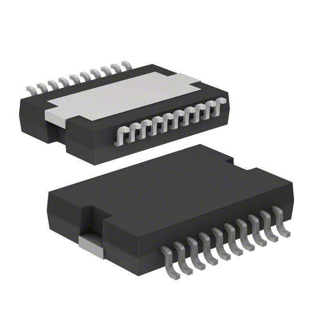
| 描述 | IC OPAMP GP 900KHZ 20PSOP |
| 产品分类 | Linear - Amplifiers - Instrumentation, OP Amps, Buffer Amps |
| 品牌 | Apex Microtechnology |
| 数据手册 | |
| 产品图片 |
|
| 产品型号 | PA162DK |
| rohs | 无铅 / 符合限制有害物质指令(RoHS)规范要求 |
| 产品系列 | Apex Precision Power® |
| 产品培训模块 | http://www.digikey.cn/PTM/IndividualPTM.page?site=cn&lang=zhs&ptm=30464 |
| 产品目录页面 | |
| 供应商器件封装 | 20-PSOP |
| 其它名称 | 598-1430 |
| 包装 | 管件 |
| 压摆率 | 1.4 V/µs |
| 增益带宽积 | 900kHz |
| 安装类型 | 表面贴装 |
| 封装/外壳 | 20-SOIC(0.433",11.00mm 宽)裸焊盘 |
| 工作温度 | -40°C ~ 125°C |
| 放大器类型 | 通用 |
| 标准包装 | 30 |
| 电压-电源,单/双 (±) | 5 V ~ 40 V, ±2.5 V ~ 20 V |
| 电压-输入失调 | 1mV |
| 电流-电源 | 16mA |
| 电流-输入偏置 | 100nA |
| 电流-输出/通道 | 1.5A |
| 电路数 | 4 |
| 输出类型 | - |
| 配用 | /product-detail/zh/EK68/598-1489-ND/1973356/product-detail/zh/EK14/EK14-ND/1762062 |


PDF Datasheet 数据手册内容提取
PAP1A61622 PA162 Power Operational Amplifiers FEATURES DESCRIPTION ♦ LOW COST The amplifier design is a dual power op amp on a ♦ WIDE BANDWIDTH - 1.1 Mhz single monolithic die. The quad output PA162 com- bines two dual op amp die in a single PSOP pack- ♦ HIGH OUTPUT CURRENT - 1.5A PER AMPLIFIER age. This approach provides a cost-effective solu- ♦ WIDE COMMON MODE RANGE Includes negative tion to applications where multiple amplifiers are supply required or a bridge configuration is needed. Four ♦ WIDE SUPPLY VOLTAGE RANGE Single supply: independent amplifiers coupled with low quiescent 5V to 40V Split supplies: ± 2.5V to ± 20V current and very low THD makes this an ideal low- ♦ LOW QUIESCENT CURRENT distortion 4-channel audio amplifier for applications ♦ VERY LOW DISTORTION such as laptops and computer speakers. APPLICATIONS The quad output PA162DK is available in a surface mount 20-pin PSOP, JEDEC MO-166-AB package. ♦ HALF AND FULL BRIDGE MOTOR DRIVERS Built-in thermal shutdown allows the devices to self- ♦ AUDIO POWER AMPLIFIER protect against thermal overloads. Care must be ex- Stereo - 11.3W RMS per amplifier ercised to observe the Safe Operating Area (SOA) Bridge - 22.6W RMS per two amplifiers curve and proper heatsinking will ensure maximum Two Bridges - 45.2W RMS per package reliability. ♦ 3 PHASE MOTOR DRIVER The wide common mode input range includes the 3 Channels - 33.9W RMS per package negative rail, facilitating single supply applications. ♦ IDEAL FOR SINGLE SUPPLY SYSTEMS This makes it possible to have a ground-based input 5V - Peripherals driving a single supply amplifier with ground acting 12V - Automotive as the second or bottom supply of the amplifier. 28V - Avionic ♦ PACKAGING OPTIONS 20-Pin PSOP, JEDEC MO-166-AB (PA162DK) +Vs I BIAS MONITOR -IN +IN OUT THERMAL PROTECT -Vs FIGURE 1. Equivalent schematic (one channel) Copyright © Apex Microtechnology, Inc. 2012 OCT 2012 PwAw1w6.2aUp e xanalog .com (All Rights Reserved) PA162U REVD1
PA162 1. CHARACTERISTICS AND SPECIFICATIONS ABSOLUTE MAXIMUM RATINGS Parameter Symbol Min Max Units SUPPLY VOLTAGE, total 5 40 V OUTPUT CURRENT SOA POWER DISSIPATION, internal (1 amplifier) 15 W POWER DISSIPATION, internal (2 amplifiers)5 24 W POWER DISSIPATION, internal (3 amplifiers)5 36 W POWER DISSIPATION, internal (4 amplifiers)5 45 W INPUT VOLTAGE, differential -Vs +Vs INPUT VOLTAGE, common mode +Vs -Vs-.5V JUNCTION TEMPERATURE, max2 150 °C TEMPERATURE, pin solder - 10 secs max. 220 °C TEMP RANGE STORAGE -55 150 °C OPERATING TEMP RANGE, case2 -40 125 °C SPECIFICATIONS (PER AMPLIFIER) Parameter Test Conditions2,3 Min Typ Max Units INPUT OFFSET VOLTAGE, initial 1 15 mV OFFSET VOLTAGE, vs. temperature Full temp range 20 µV/°C BIAS CURRENT, initial 100 500 nA COMMON MODE RANGE Full temp range -Vs +Vs V COMMON MODE REJECTION, DC 60 90 dB POWER SUPPLY REJECTION Full temp range 60 90 dB CHANNEL SEPARATION I = 500mA, ƒ = 1kHz 50 68 dB OUT INPUT NOISE VOLTAGE R = 100Ω, ƒ = 1 to 100kHz 22 nV/√Hz S GAIN OPEN LOOP GAIN V = ±10V, R = 2.0KΩ 89 100 dB O L GAIN BANDWIDTH PRODUCT ƒ = 100kHz, C = 100pF, R = 2.0KΩ 0.9 1.4 MHz L L PHASE MARGIN Full temp range 65 °C POWER BANDWIDTH V (P-P) = 28V 13.6 kHz O OUTPUT CURRENT, peak 1.5 A CURRENT, continuous 1 A SLEW RATE 1.0 1.4 V/µS VOLTAGE SWING Full temp range, I = 100mA |Vs| -1.1 |Vs| -0.8 V O VOLTAGE SWING Full temp range, I = 1A |Vs| -1.8 |Vs| -1.4 V O HARMONIC DISTORTION A = 1, R = 50Ω, .02 % V L V = .5VRMS, ƒ = 1kHz O 2 PA162U
PA162 Parameter Test Conditions2,3 Min Typ Max Units POWER SUPPLY VOLTAGE, Vss4 5 30 40 V CURRENT, quiescent +Vs (A/B) 8 10 mA CURRENT, quiescent +Vs (C/D) 8 10 mA CURRENT, quiescent total 16 20 mA THERMAL RESISTANCE, junction to case DC, 1 amplifier 7.16 7.87 °C/W DC, 2 amplifiers5 4.69 5.16 °C/W DC, 3 amplifiers5 3.08 3.39 °C/W DC, 4 amplifiers5 2.51 2.77 °C/W AC, 1 amplifier 5.37 5.90 °C/W AC, 2 amplifiers5 3.52 3.87 °C/W AC, 3 amplifiers5 2.31 2.54 °C/W AC, 4 amplifiers5 1.89 2.07 °C/W RESISTANCE, junction to air7 25 °C/W NOTES: 1. (All Min/Max characteristics and specifications are guaranteed over the Specified Operating Condi- tions. Typical performance characteristics and specifications are derived from measurements taken at typical supply voltages and T = 25°C). C 2. Long term operation at the maximum junction temperature will result in reduced product life. Derate power dissipation to achieve high MTTF. 3. Unless otherwise noted, the following conditions apply: ±V = ±15V, T =25°C. S C 4. +V and -V denote the positive and negative rail respectively. V denotes total rail-to-rail supply. S S SS 5. Rating applies when power dissipation is equal in each of the amplifiers. Power and thermal ratings are based on two separate dual monolithic power op-amps on one integrated copper heatslug. Amplifiers A and B are combined on one monolithic die while amplifiers C and D are on the other. 6. If -V is disconnected before +V , a diode between -V and ground is recommended to avoid dam- S S s age. 7. Rating applies when the heatslug of the DK package is soldered to a minimum of 1 square inch foil area of a printed circuit board. 1 20 NC -VS -IN(A) - OUT(A) A +IN(A) + +VS(A/B) +IN(B) + OUT(B) -IN(B) -B -VS -IN(C) - -VS C +IN(C) + OUT(C) 20-pin PSOP +IN(D) + +VS(C/D) -IN(D) -D OUT(D) PACKAGE STYLE DK NC -VS 10 11 FIGURE 2. EXTERNAL CONNECTIONS. PA162U 3
PA162 TYPICAL PERFORMANCE GRAPHS QUIESCENT CURRENT BIAS CURRENT VOS 75 V) PPLY VOLTAGE, V (V) S 2112608 1480200 0 MPERATURE, T (°C) C BIAS CURRENT, I (mA) B 5655 FSET VOLTAGE, V (mOS 32 TOTAL SU 40 --8400 CASE TE AVERAGE 45 VERAGE OF 01 2 4 6 8 10 -40 0 40 80 120 A -40 0 40 80 120 AVERAGE QUIESCENT CURRENT, I (mA) CASE TEMPERATURE, T (°C) CASE TEMPERATURE, T (°C) Q C C PHASE MARGIN vs. OUTPUT LOAD CAPACITANCE VOLTAGE GAIN & PHASE vs. FREQUENCY OUTPUT VOLTAGE SWING 2 HASE MARGIN, Ф (°) 564555 GAIN, A (dB) 246000 91110000 PHASE, Ф (°) DROP FROM SUPPLY, (V) 101101......4862681 P 35 0 120 GE 0.4 A LT 0.2 O 25 -20 130 V 0 00 04 08 12 16 20 1 10 100 1K 10K 0.1 0.2 0.3 0.4 0.5 0.6 0.7 0.8 0.9 1.0 OUTPUT LOAD CAPACITANCE, C (nF) FREQUENCY, ƒ (KHz) OUTPUT CURRENT, I (A) L O PULSE RESPONSE PULSE RESPONSE 10 10 8 8 (V) O 6 +VAS = = + +115 V (V) O 6 +VAS = = + +115 V GE, V 42 VIN V= 10Vp GE, V 42 VIN V= 10Vp A A LT 0 LT 0 O O V -2 V -2 T T OUTPU --46 f-IRVN SL= ==2 02-1k05HΩVz OUTPU --46 -fVINS = = 1 -k1H5Vz -8 -8 -10 -10 0 10 20 30 40 50 60 70 0 200 400 600 800 1000 1200 1400 TIME, t (µs) TIME, t (µs) TYPICAL APPLICATION R2 R3 R1 and R2 set up Amplifier A as non-inverting. Ampli- R4 fier B is set up as a unity gain inverter driven from the +28V output of Amplifier A. Note that Amplifier B inverts the R1 _ _ signals about the reference node, which is set at mid- A B supply by R5 and R6. When the command input is 1/4 PA162 M 1/4 PA162 R5 INPUT + + midrange, so is the output of Amplifier A. Since this is 0-10V also equivalent to the reference node voltage, the out- R6 put of Amplifier B is the same resulting in 0V across the motor. Inputs more positive than 5V result in motor FIGURE 3. BI-DIRECTIONAL SPEED CONTROL current flow from left to right (see Figure 3). Inputs less FROM A SINGLE SUPPLY. than 5V drive the motor in the opposite direction. 4 PA162U
PA162 TYPICAL APPLICATION (CONT) The amplifiers are especially well-suited for applications such as this. The extended common mode range allows command inputs as low as 0V. The output swing lets it drive within 2V of the supply at an output of 1A. This means that a command input that ranges from 0 to 10V will drive a 24V motor from full scale CCW to full scale N o CW at ±1A. S -Vs (pins 11, 15, 16 and 20) must be tied to the heatslug externally on the PCB. To ease metal routing on the PCB, run a direct trace from the -Vs pin to the center heat slug. The PA162 can be used in a three amplifier configuration for a three phase inverter or motor as shown in Figure 4. Using 3 amplifiers from PA162 GENERAL PA162 as 3 phase motor driver. Quad Please read Application Note 1 "General Operating Con- siderations" which covers stability, supplies, heatsinking, FIGURE 4. 3 Phase Inverter mounting, SOA interpretation, and specification interpre- tation. Visit www.apexanalog.com for design tools that help automate tasks such as calculations for stability, internal power dissipation, heatsink selection; Apex Microtechnology's complete Application Notes library; Technical Semi- nar Workbook; and Evaluation Kits. STABILITY CONSIDERATIONS + All monolithic power op amps use output stage topologies that present special sta- bility problems. This is primarily due to non-complementary (both devices are NPN) – C output stages with a mismatch in gain and phase response for different polarities of SN 0.01µF output current. It is difficult for the op amp manufacturer to optimize compensation for all operating conditions. For applications with load current exceeding 300mA, R oscillation may appear. The oscillation may occur only with the output voltage swing 10SΩN at the negative or positive half cycle. Under most operating and load conditions acceptable stability can be achieved by providing a series RC snubber network connected from the output to ground (see Figure 5). The recommended component FIGURE 5. R-C Snubber values of the network are, R = 10Ω and C = 0.01µF. Please refer to Application SN SN Note 1 for further details. SAFE OPERATING AREA (SOA) SOA The SOA curves combine the effect of all limits for this A)10 power op amp. For a given application, the direction and V, (S DC, TC = 25°C magnitude of the output current should be calculated or R - O DC, T = 85°C measured and checked against the SOA curves. This is S C V simple for resistive loads but more complex for reactive M + and EMF generating loads. The following guidelines may O R save extensive analytical efforts. F 1 T N 4 AMPLIFIERS LOADED E R 3 AMPLIFIERS LOADED R U 2 AMPLIFIERS LOADED C T 1 AMPLIFIER LOADED U P T U O 0.1 1 10 50 SUPPLY TO OUTPUT DIFFERENTIAL VOLTAGE, V - V (V) S O PA162U 5
PA162 THERMAL CONSIDERATIONS POWER DERATING The PA162DK has a large exposed integrated copper heat- 50 scffSiWiissnooloou girhrnlnmlg e.dean e qSaerrteceoeunruec aicrctrtswfhi eeoosaohed anncfoi cren Ptffyhooh eA m2efr ct 1to5 mhttop6hi °oeuruCi2einn nnsD m/i htteWmt eKooet deas naija culsuoct nhspr nliufir lnoatcucashiwctugqreiieecoi eudtt a n reo ibms i nsa oot aoo d pfaih u nipr1rmaincgdel iiltrhct icu nwo aettrdi leiamtyr2leicl to p iaurhsnnteohtmnqgstsweaiu . quo ceoauulhftrfr se eeita1nesh dp i ent.osoph cqTfflPe i hcuahhAreaam ee1sstr aiau6e sootlor2 sn ffiplDnai sdnfecc,oKek rheiir--.tl AL POWER DISSIPATION, P (W) 324000 (A+(((AAAB+++)B BCA+))CM AA+PMMDL)PP IAFLLMIIIFEFPIIRELERI RFLSISOE L RALOSODA LEADODDEAEDDDED mount fan in combination with a surface mount heatsink on RN 10 E the backside of the FR4/ PC board with through hole ther- T N mal vias. Other highly thermal conductive substrate board I 0 materials are available for maximum heat sinking. 0 25 50 75 100 125 The Power Derating graph assumes that the power dissipa- JUNCTION TEMPERATURE, TJ (°C) tion is equal in each of the amplifiers. Power and thermal ratings are based on two separate dual monolithic power op amps on one integrated copper heat slug. Amps A and B are combined on one monolithic die while amps C and D are combined on the other. This multi chip configura- tion provides superior thermal performance by isolating each of the dual amplifiers. When loading either of the dual amplifiers it is possible to achieve better thermal performance by loading any combination of amplifiers (A or B) + (C or D). MOUNTING PRECAUTIONS 1. Always use a heat sink. Even unloaded the PA162DK can dissipate up to .8 watts. 2. Avoid bending the leads. Such action can lead to internal damage. NEED TECHNICAL HELP? CONTACT APEX SUPPORT! For all Apex Microtechnology product questions and inquiries, call toll free 800-546-2739 in North America. For inquiries via email, please contact apex.support@apexanalog.com. International customers can also request support by contacting their local Apex Microtechnology Sales Representative. To find the one nearest to you, go to www.apexanalog.com IMPORTANT NOTICE Apex Microtechnology, Inc. has made every effort to insure the accuracy of the content contained in this document. However, the information is subject to change without notice and is provided "AS IS" without warranty of any kind (expressed or implied). Apex Microtechnology reserves the right to make changes without further notice to any specifications or products mentioned herein to improve reliability. This document is the property of Apex Microtechnology and by furnishing this informa- tion, Apex Microtechnology grants no license, expressed or implied under any patents, mask work rights, copyrights, trademarks, trade secrets or other intellectual property rights. Apex Microtechnology owns the copyrights associated with the information contained herein and gives consent for copies to be made of the informa- tion only for use within your organization with respect to Apex Microtechnology integrated circuits or other products of Apex Microtechnology. This consent does not extend to other copying such as copying for general distribution, advertising or promotional purposes, or for creating any work for resale. APEX MICROTECHNOLOGY PRODUCTS ARE NOT DESIGNED, AUTHORIZED OR WARRANTED TO BE SUITABLE FOR USE IN PRODUCTS USED FOR LIFE SUPPORT, AUTOMOTIVE SAFETY, SECURITY DEVICES, OR OTHER CRITICAL APPLICATIONS. PRODUCTS IN SUCH APPLICATIONS ARE UNDER- STOOD TO BE FULLY AT THE CUSTOMER OR THE CUSTOMER’S RISK. Apex Microtechnology, Apex and Apex Precision Power are trademarks of Apex Microtechnolgy, Inc. All other corporate names noted herein may be trademarks of their respective holders. Copyright © Apex Microtechnology, Inc. 2012 OCT 2012 6w ww.ape xanalog .com (All Rights Reserved) P A 1 6 2 U P AR1E6V2DU