ICGOO在线商城 > 射频/IF 和 RFID > RF 天线 > PA.22A
 Datasheet下载
- 型号: PA.22A
- 制造商: Taoglas Limited
- 库位|库存: xxxx|xxxx
- 要求:
| 数量阶梯 | 香港交货 | 国内含税 |
| +xxxx | $xxxx | ¥xxxx |
查看当月历史价格
查看今年历史价格
PA.22A产品简介:
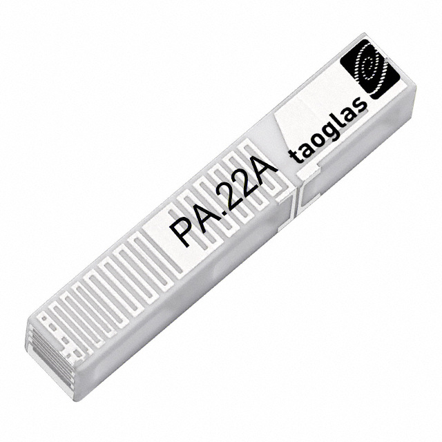
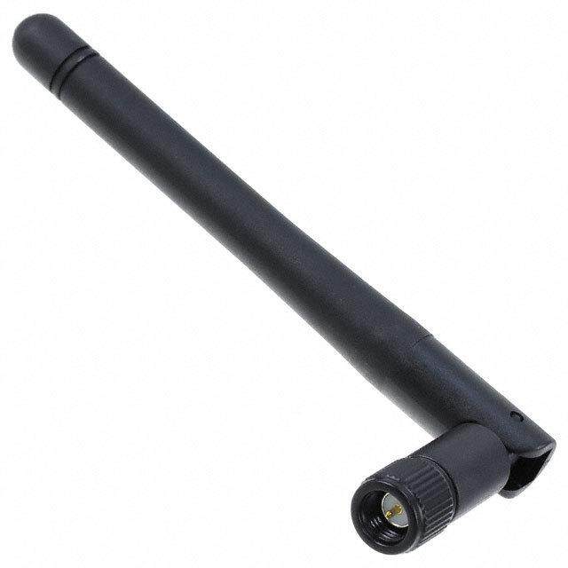
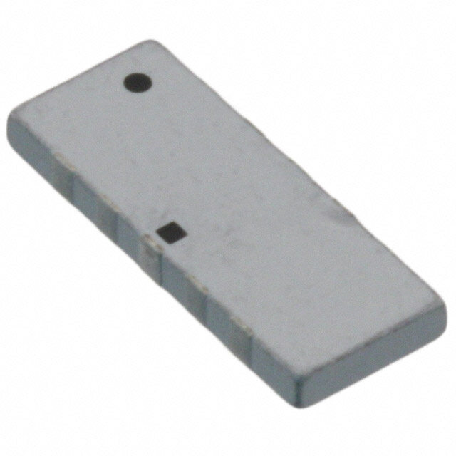
ICGOO电子元器件商城为您提供PA.22A由Taoglas Limited设计生产,在icgoo商城现货销售,并且可以通过原厂、代理商等渠道进行代购。 PA.22A价格参考。Taoglas LimitedPA.22A封装/规格:RF 天线, 920MHz,1.9GHz GSM 芯片 RF 天线 880MHz ~ 960MHz,1.71GHz ~ 1.99GHz -1.96dBi,2.48dBi 焊接 表面贴装。您可以下载PA.22A参考资料、Datasheet数据手册功能说明书,资料中有PA.22A 详细功能的应用电路图电压和使用方法及教程。
Taoglas Limited的PA.22A是一款高性能的RF(射频)天线,专为需要稳定和高效无线连接的应用场景设计。该天线支持多种无线通信协议,如Wi-Fi、蓝牙和蜂窝网络,广泛应用于物联网(IoT)、智能城市、工业自动化和车联网等领域。

在物联网设备中,PA.22A适用于远程监控、传感器网络和智能家居设备,确保设备在复杂环境中保持稳定通信。在工业自动化中,它可用于PLC(可编程逻辑控制器)、远程终端单元(RTU)和工业网关,提供可靠的无线连接,支持工业4.0的发展需求。

此外,PA.22A也适用于移动设备和车载系统,如车载通信模块、无人机通信系统和移动热点设备,满足高速移动场景下的信号稳定性需求。其紧凑的设计和多频段支持能力,使其能够在有限空间内实现高性能通信。

总的来说,PA.22A适用于需要高性能、多频段支持和稳定无线连接的各类RF通信场景。
| 参数 | 数值 |
| 产品目录 | |
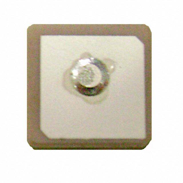
| 描述 | GSM DIELECTRIC PIFA ANTENNA天线 TRIBND CELL ANT 900/1800/1900MHZ |
| 产品分类 | |
| 品牌 | Taoglas |
| 产品手册 | |
| 产品图片 |
|
| rohs | 符合RoHS无铅 / 符合限制有害物质指令(RoHS)规范要求 |
| 产品系列 | Taoglas PA.22a- |
| mouser_ship_limit | 该产品可能需要其他文档才能发货到中国。 |
| 数据手册 | |
| 产品型号 | PA.22a |
| VSWR | 2.5 |
| 产品种类 | 天线 |
| 其它名称 | 931-1116-6 |
| 包装 | Digi-Reel® |
| 商标 | Taoglas |
| 增益 | 0dB |
| 天线类型 | 芯片 |
| 安装类型 | 表面贴装 |
| 宽度 | 6 mm |
| 封装 | Bulk |
| 尺寸 | 29.8 mm L x 6 mm W x 5 mm H |
| 应用说明 | |
| 技术类型 | GSM Dielectric PIFA Antenna |
| 标准包装 | 1 |
| 端接 | 表面贴装型 |
| 端接类型 | SMD/SMT |
| 长度 | 29.8 mm |
| 阻抗 | 50 Ohms |
| 频带数 | 3 |
| 频率 | 900 MHz, 1800 MHz, 1900 MHz |
| 高度 | 5 mm |
| 高度(最大值) | 0.236"(6.00mm) |


- 商务部:美国ITC正式对集成电路等产品启动337调查
- 曝三星4nm工艺存在良率问题 高通将骁龙8 Gen1或转产台积电
- 太阳诱电将投资9.5亿元在常州建新厂生产MLCC 预计2023年完工
- 英特尔发布欧洲新工厂建设计划 深化IDM 2.0 战略
- 台积电先进制程称霸业界 有大客户加持明年业绩稳了
- 达到5530亿美元!SIA预计今年全球半导体销售额将创下新高
- 英特尔拟将自动驾驶子公司Mobileye上市 估值或超500亿美元
- 三星加码芯片和SET,合并消费电子和移动部门,撤换高东真等 CEO
- 三星电子宣布重大人事变动 还合并消费电子和移动部门
- 海关总署:前11个月进口集成电路产品价值2.52万亿元 增长14.8%


PDF Datasheet 数据手册内容提取
SPECIFICATION PA.22A Part No. : Product Name : Dielectric PIFA Antenna Description : Tri-band - 880~960 MHz, 1710~1990 MHz, 0dB Gain Size: 29.8mm*6mm*5mm RoHS Compliant SPE-11-8-060/G Page 1 of 24
1. Scope This specification is for a Tri-band GSM miniature PIFA (Dielectric Planar Inverted-F Type Antenna) (DPA™) Antenna for internal SMT mounting. Note: The antenna also shows a response at 850MHz which means the antenna can also be defined on quad-band, depending on the target specification for the device itself. 2. Electrical Specifications The antenna has the electrical characteristics given in Table 1 under the Taoglas standard installation conditions as shown in the Evaluation Board (Figure No. Parameter Specification 1 Frequency 880~960 MHz , 1710~1990 MHz 2 Dimensions 29.8*6.0*5.0 mm 3 Impedance 50 Ω 4 VSWR 2.5 max (depends on environment) 5 Polarization Linear 6 Operating Temperature -40~85°C Ag (Environmentally Friendly Lead- 7 Termination Free) *Data is measured on Taoglas Evaluation Board (reference ground plane) pictured below SPE-11-8-060/G Page 2 of 24
2.1 S11 Response Curve SPE-11-8-060/G Page 3 of 24
Radiation patterns also available (measured in free space and on evaluation board) SPE-11-8-060/G Page 4 of 24
2.2 Gain and Efficiency SPE-11-8-060/G Page 5 of 24
SPE-11-8-060/G Page 6 of 24
SPE-11-8-060/G Page 7 of 24
SPE-11-8-060/G Page 8 of 24
SPE-11-8-060/G Page 9 of 24
SPE-11-8-060/G Page 10 of 24
SPE-11-8-060/G Page 11 of 24
SPE-11-8-060/G Page 12 of 24
SPE-11-8-060/G Page 13 of 24
SPE-11-8-060/G Page 14 of 24
SPE-11-8-060/G Page 15 of 24
SPE-11-8-060/G Page 16 of 24
3. Mechanical Dimensions 3.1 PA.22 Antenna feed to module to ground solder pads (mechanical only) SPE-11-8-060/G Page 17 of 24
3.2Evaluation board dimensions SPE-11-8-060/G Page 18 of 24
3.3 Recommended layout (as per Taoglas evalution board) Non metal area 4.7nH inductor 6mm clearance ideally For EVB only to ground (minimum 4mm clearance) feed to mod ule View from underneath board – note solder pads either side – laid out on non metal area Layout dimensions - Allow 6mm clearance all around if possible (minimum 4mm) SPE-11-8-060/G Page 19 of 24
SPE-11-8-060/G Page 20 of 24
3.4 Recommended Transmission Line and Matching Network Note: The PA.22 can be made “quad band” with appropriate matching circuit Guidelines for routing RF when designing a PCB; 1) Good 2) Bad SPE-11-8-060/G Page 21 of 24
4. Packaging SPE-11-8-060/G Page 22 of 24
SPE-11-8-060/G Page 23 of 24
5. Recommended Reflow Temperature Profile (1) Time shown in the above figures is measured from the point when chip surface reaches temperature. (2) Temperature difference in high temperature part should be within 110°C. (3) After soldering, do not force cool, allow the parts to cool gradually. *General attention to soldering: ● High soldering temperatures and long soldering times can cause leaching of the termination, decrease in adherence strength, and the change of characteristic may occur. ● for soldering, please refer to the soldering curves above. However, please keep exposure to temperatures exceeding 200°C to under 50 seconds. ● please use a mild flux (containing less than 0.2wt% Cl). Also, if the flux is water soluble, be sure to wash thoroughly to remove any residue from the underside of components that could affect resistance. Cleaning: When using ultrasonic cleaning, the board may resonate if the output power is too high. Since this vibration can cause cracking or a decrease in the adherence of the termination, we recommend that you use the conditions below. Frequency: 40 kHz max. - Output power: 20W/Iiter -Cleaning time: 5minutes max. SPE-11-8-060/G Page 24 of 24