ICGOO在线商城 > 集成电路(IC) > 嵌入式 - 微控制器 > P89LPC924FDH,518

 Datasheet下载
- 型号: P89LPC924FDH,518
- 制造商: NXP Semiconductors
- 库位|库存: xxxx|xxxx
- 要求:
| 数量阶梯 | 香港交货 | 国内含税 |
| +xxxx | $xxxx | ¥xxxx |
查看当月历史价格
查看今年历史价格
P89LPC924FDH,518产品简介:
ICGOO电子元器件商城为您提供P89LPC924FDH,518由NXP Semiconductors设计生产,在icgoo商城现货销售,并且可以通过原厂、代理商等渠道进行代购。 P89LPC924FDH,518价格参考。NXP SemiconductorsP89LPC924FDH,518封装/规格:嵌入式 - 微控制器, 8051 微控制器 IC LPC900 8-位 18MHz 4KB(4K x 8) 闪存 20-TSSOP。您可以下载P89LPC924FDH,518参考资料、Datasheet数据手册功能说明书,资料中有P89LPC924FDH,518 详细功能的应用电路图电压和使用方法及教程。
NXP USA Inc.生产的P89LPC924FDH,518是一款嵌入式微控制器,广泛应用于各种工业、消费电子和汽车领域。以下是其主要应用场景:

 1. 工业自动化
P89LPC924FDH,518在工业自动化中主要用于控制和监测系统。它具备丰富的I/O接口,能够与传感器、执行器等设备连接,实现对生产线的实时监控和控制。例如,在工厂自动化中,它可以用于电机控制、温度监控、压力检测等,确保生产过程的稳定性和高效性。

 2. 消费电子产品
该微控制器适用于多种消费电子产品,如智能家居设备、家电控制板等。其低功耗设计和高集成度使其成为这些应用的理想选择。例如,在智能门锁、智能插座、智能灯具等产品中,P89LPC924FDH,518可以提供可靠的控制功能,同时保持较低的能耗,延长电池寿命。

 3. 汽车电子
在汽车电子领域,P89LPC924FDH,518可用于车身控制模块(BCM)、车载信息娱乐系统、发动机管理等。它的高可靠性和抗干扰能力使其能够在复杂的汽车环境中稳定工作。例如,在车身控制系统中,它可以控制车窗升降、车灯开关、雨刷等功能,提升驾驶体验和安全性。

 4. 医疗设备
该微控制器也适用于医疗设备,如血糖仪、心率监测仪、血压计等便携式医疗设备。其内置的ADC(模数转换器)可以精确采集生理信号,而低功耗特性则有助于延长设备的工作时间。此外,其小型化设计使得它非常适合用于便携式医疗设备中。

 5. 物联网(IoT)
P89LPC924FDH,518在物联网应用中表现出色,尤其是在需要低功耗和高可靠性的小型节点上。它可以作为传感器节点的核心控制器,负责数据采集、处理和传输。例如,在环境监测系统中,它可以用于空气质量监测、温湿度监测等,通过无线通信模块将数据发送到云端进行分析。

总之,P89LPC924FDH,518凭借其高性能、低功耗和高集成度,广泛应用于多个领域,为各种嵌入式系统提供了可靠的控制解决方案。
| 参数 | 数值 |
| A/D位大小 | 8 bit |
| 产品目录 | 集成电路 (IC)半导体 |
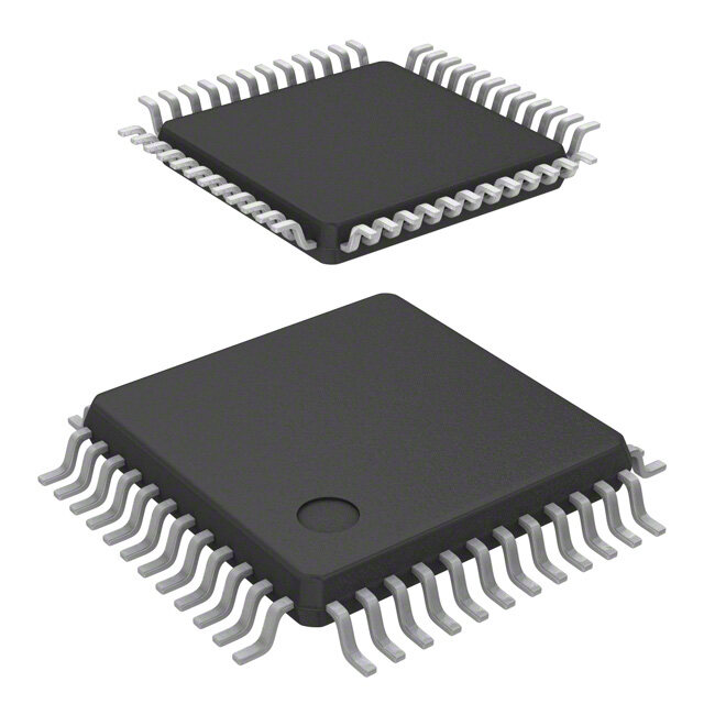
| 描述 | IC 80C51 MCU FLASH 4K 20TSSOP8位微控制器 -MCU 4K FL/256B |
| EEPROM容量 | - |
| 产品分类 | |
| I/O数 | 18 |
| 品牌 | NXP Semiconductors |
| 产品手册 | |
| 产品图片 |
|
| rohs | 符合RoHS无铅 / 符合限制有害物质指令(RoHS)规范要求 |
| 产品系列 | 嵌入式处理器和控制器,微控制器 - MCU,8位微控制器 -MCU,NXP Semiconductors P89LPC924FDH,518LPC900 |
| 数据手册 | |
| 产品型号 | P89LPC924FDH,518 |
| RAM容量 | 256 x 8 |
| 产品目录页面 | |
| 产品种类 | 8位微控制器 -MCU |
| 供应商器件封装 | 20-TSSOP |
| 其它名称 | 568-4338-6 |
| 包装 | Digi-Reel® |
| 可用A/D通道 | 4 |
| 可编程输入/输出端数量 | 15 |
| 商标 | NXP Semiconductors |
| 商标名 | LPC |
| 处理器系列 | P89LPC9x |
| 外设 | 欠压检测/复位,LED,POR,PWM,WDT |
| 安装风格 | SMD/SMT |
| 定时器数量 | 2 Timer |
| 封装 | Reel |
| 封装/外壳 | 20-TSSOP(0.173",4.40mm 宽) |
| 封装/箱体 | TSSOP-20 |
| 工作温度 | -40°C ~ 85°C |
| 工作电源电压 | 2.4 V to 3.6 V |
| 工厂包装数量 | 2500 |
| 振荡器类型 | 内部 |
| 接口类型 | I2C, SPI, UART |
| 数据RAM大小 | 256 B |
| 数据Ram类型 | RAM |
| 数据总线宽度 | 8 bit |
| 数据转换器 | A/D 4x8b; D/A 1x8b |
| 最大工作温度 | + 85 C |
| 最大时钟频率 | 18 MHz |
| 最小工作温度 | - 40 C |
| 标准包装 | 1 |
| 核心 | 80C51 |
| 核心处理器 | 8051 |
| 核心尺寸 | 8-位 |
| 片上ADC | Yes |
| 片上DAC | Without DAC |
| 电压-电源(Vcc/Vdd) | 2.4 V ~ 3.6 V |
| 电源电压-最大 | 3.6 V |
| 电源电压-最小 | 2.4 V |
| 程序存储器大小 | 4 kB |
| 程序存储器类型 | 闪存 |
| 程序存储容量 | 4KB(4K x 8) |
| 系列 | 89LP |
| 输入/输出端数量 | 15 I/O |
| 连接性 | I²C, UART/USART |
| 速度 | 18MHz |
| 配用 | /product-detail/zh/DB-TSSOP-SKT/622-1014-ND/1642806/product-detail/zh/DB-HVSON10-LPC9103/622-1008-ND/1642800/product-detail/zh/USB-ICP-SAB9/622-1006-ND/1628379/product-detail/zh/OM6273,598/568-4000-ND/1213115/product-detail/zh/OM6270,598/568-3510-ND/1129868/product-detail/zh/USB-ICP-LPC9XX/622-1002-ND/1010439/product-detail/zh/EPM900/568-1759-ND/765293 |
| 零件号别名 | P89LPC924FDH-T |

.jpg)


- 商务部:美国ITC正式对集成电路等产品启动337调查
- 曝三星4nm工艺存在良率问题 高通将骁龙8 Gen1或转产台积电
- 太阳诱电将投资9.5亿元在常州建新厂生产MLCC 预计2023年完工
- 英特尔发布欧洲新工厂建设计划 深化IDM 2.0 战略
- 台积电先进制程称霸业界 有大客户加持明年业绩稳了
- 达到5530亿美元!SIA预计今年全球半导体销售额将创下新高
- 英特尔拟将自动驾驶子公司Mobileye上市 估值或超500亿美元
- 三星加码芯片和SET,合并消费电子和移动部门,撤换高东真等 CEO
- 三星电子宣布重大人事变动 还合并消费电子和移动部门
- 海关总署:前11个月进口集成电路产品价值2.52万亿元 增长14.8%


PDF Datasheet 数据手册内容提取
P89LPC924/925 8-bit microcontrollers with accelerated two-clock 80C51 core 4 kB/8 kB 3 V low-power Flash with 8-bit A/D converter Rev. 03 — 15 December 2004 Product data 1. General description TheP89LPC924/925 are single-chip microcontrollers designed for applications demanding high-integration, low cost solutions over a wide range of performance requirements. TheP89LPC924/925 is based on a high performance processor architecture that executes instructions in two to four clocks, six times the rate of standard 80C51 devices. Many system-level functions have been incorporated into theP89LPC924/925 in order to reduce component count, board space, and system cost. 2. Features 2.1 Principal features n 4kB/8kBFlashcodememorywith1kBerasablesectors,64-byteerasablepage size, and single byte erase. n 256-byte RAM data memory. n Two 16-bit counter/timers. Each timer may be configured to toggle a port output upon timer overflow or to become a PWM output. n Real-Time clock that can also be used as a system timer. n 4-input 8-bit multiplexed A/D converter/single DAC output. Two analog comparators with selectable inputs and reference source. n Enhanced UART with fractional baudrate generator, break detect, framing error detection, automatic address detection and versatile interrupt capabilities. n 400kHz byte-wide I2C-bus communication port. n Configurable on-chip oscillator with frequency range and RC oscillator options (selectedbyuserprogrammedFlashconfigurationbits).TheRCoscillator(factory calibrated to– 1%) option allows operation without external oscillator components.Oscillatoroptionssupportfrequenciesfrom20kHztothemaximum operating frequency of 18MHz. The RC oscillator option is selectable and fine tunable. n 2.4Vto3.6VV operatingrange.I/Opinsare5Vtolerant(maybepulledupor DD driven to 5.5V). n 15 I/O pins minimum. Up to 18 I/O pins while using on-chip oscillator and reset options.
P89LPC924/925 Philips Semiconductors 8-bit microcontrollers with accelerated two-clock 80C51 core 2.2 Additional features n 20-pin TSSOP package. n A high performance 80C51 CPU provides instruction cycle times of 111ns to 222ns for all instructions except multiply and divide when executing at 18MHz. This is sixtimes the performance of the standard 80C51 running at the same clock frequency. A lower clock frequency for the same performance results in power savings and reduced EMI. n In-Application Programming of the Flash code memory. This allows changing the code in a running application. n Serial Flash programming allows simple in-circuit production coding. Flash security bits prevent reading of sensitive application programs. n Watchdog timer with separate on-chip oscillator, requiring no external components. The watchdog prescaler is selectable from eight values. n Low voltage reset (Brownout detect) allows a graceful system shutdown when power fails. May optionally be configured as an interrupt. n IdleandtwodifferentPower-downreducedpowermodes.Improvedwake-upfrom Power-down mode (a low interrupt input starts execution). Typical Power-down current is 1m A (total Power-down with voltage comparators disabled). n Active-LOWreset.On-chippower-onresetallowsoperationwithoutexternalreset components. A reset counter and reset glitch suppression circuitry prevent spurious and incomplete resets. A software reset function is also available. n Oscillator Fail Detect. The watchdog timer has a separate fully on-chip oscillator allowing it to perform an oscillator fail detect function. n Programmable port output configuration options: u quasi-bidirectional, u open drain, u push-pull, u input-only. n Port‘inputpatternmatch’detect.Port0maygenerateaninterruptwhenthevalue of the pins match or do not match a programmable pattern. n LED drive capability (20mA) on all port pins. A maximum limit is specified for the entire chip. n Controlled slew rate port outputs to reduce EMI. Outputs have approximately 10ns minimum ramp times. n Only power and ground connections are required to operate the P89LPC924/925 when internal reset option is selected. n Four interrupt priority levels. n Eight keypad interrupt inputs, plus two additional external interrupt inputs. n Second data pointer. n Schmitt trigger port inputs. n Emulation support. 9397 750 14471 © Koninklijke Philips Electronics N.V. 2004. All rights reserved. Product data Rev. 03 — 15 December 2004 2 of 49
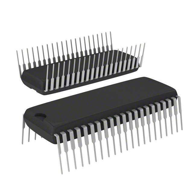
P89LPC924/925 Philips Semiconductors 8-bit microcontrollers with accelerated two-clock 80C51 core 3. Ordering information Table 1: Ordering information Type number Package Name Description Version P89LPC924FDH TSSOP20 plastic thin shrink small outline package; SOT360-1 20leads; body width 4.4mm P89LPC925FDH TSSOP20 plastic thin shrink small outline package; SOT360-1 20leads; body width 4.4mm 3.1 Ordering options Table 2: Part options Type number Flash memory Temperature range Frequency P89LPC924FDH 4kB - 40(cid:176) Cto+85(cid:176) C 0MHzto18MHz P89LPC925FDH 8kB - 40(cid:176) Cto+85(cid:176) C 0MHzto18MHz 9397 750 14471 © Koninklijke Philips Electronics N.V. 2004. All rights reserved. Product data Rev. 03 — 15 December 2004 3 of 49
P89LPC924/925 Philips Semiconductors 8-bit microcontrollers with accelerated two-clock 80C51 core 4. Block diagram P89LPC924/925 HIGH PERFORMANCE ACCELERATED 2-CLOCK 80C51 CPU 2 kB/4 kB/8 kB UART CODE FLASH INTERNAL BUS 256-BYTE REAL-TIME CLOCK/ DATA RAM SYSTEM TIMER PORT 3 I2C CONFIGURABLE I/Os PORT 1 TIMER 0 CONFIGURABLE I/Os TIMER 1 PORT 0 WATCHDOG TIMER CONFIGURABLE I/Os AND OSCILLATOR KEYPAD ANALOG INTERRUPT COMPARATORS PROGRAMMABLE CPU OSCILLATOR DIVIDER CLOCK ADC1/DAC1 CRYSTAL CONFIGURABLE ON-CHIP OR OSCILLATOR RC RESONATOR OSCILLATOR POWER MONITOR (POWER-ON RESET, BROWNOUT RESET) 002aaa786 Fig 1. Block diagram. 9397 750 14471 © Koninklijke Philips Electronics N.V. 2004. All rights reserved. Product data Rev. 03 — 15 December 2004 4 of 49
P89LPC924/925 Philips Semiconductors 8-bit microcontrollers with accelerated two-clock 80C51 core 5. Pinning information 5.1 Pinning handbook, halfpage KBI0/CMP2/P0.0 1 20 P0.1/CIN2B/KBI1/AD10 P1.7 2 19 P0.2/CIN2A/KBI2/AD11 P1.6 3 18 P0.3/CIN1B/KBI3/AD12 RST/P1.5 4 HH 17 P0.4/CIN1A/KBI4/AD13/DAC1 DD FF VSS 5 2425 16 P0.5/CMPREF/KBI5 99 XTAL1/P3.1 6 PCPC 15 VDD LL CLKOUT/XTAL2/P3.0 7 8989 14 P0.6/CMP1/KBI6 PP INT1/P1.4 8 13 P0.7/T1/KBI7 SDA/INT0/P1.3 9 12 P1.0/TXD SCL/T0/P1.2 10 11 P1.1/RXD 002aaa787 Fig 2. TSSOP20 pin configuration. 9397 750 14471 © Koninklijke Philips Electronics N.V. 2004. All rights reserved. Product data Rev. 03 — 15 December 2004 5 of 49
P89LPC924/925 Philips Semiconductors 8-bit microcontrollers with accelerated two-clock 80C51 core 5.2 Pin description Table 3: Pin description Symbol Pin Type Description P0.0 - P0.7 1, 20, 19, I/O Port0:Port0 is an 8-bit I/O port with a user-configurable output type. During reset 18,17,16, Port0 latches are configured in the input only mode with the internal pull-up disabled. 14, 13 TheoperationofPort0pinsasinputsandoutputsdependsupontheportconfiguration selected. Each port pin is configured independently. Refer toSection 8.13.1 “Port configurations” andTable 8 “DC electrical characteristics” for details. The Keypad Interrupt feature operates with Port0 pins. All pins have Schmitt triggered inputs. Port0 also provides various special functions as described below: 1 I/O P0.0 —Port0 bit0. O CMP2 —Comparator2 output. I KBI0 —Keyboard input 0. 20 I/O P0.1 —Port0 bit1. I CIN2B —Comparator2 positive input B. I KBI1 —Keyboard input 1. I AD10 —ADC1 channel 0 analog input. 19 I/O P0.2 —Port0 bit2. I CIN2A —Comparator2 positive input A. I KBI2 —Keyboard input 2. I AD11 —ADC1 channel 1analog input. 18 I/O P0.3 —Port0 bit3. I CIN1B —Comparator1 positive input B. I KBI3 —Keyboard input 3. I AD12 —ADC1 channel 2 analog input. 17 I/O P0.4 —Port0 bit4. I CIN1A —Comparator1 positive input A. I KBI4 —Keyboard input 4. I AD13 —ADC1 channel 3 analog input. I DAC1 —Digital-to-analog converter output 1. 16 I/O P0.5 —Port0 bit5. I CMPREF —Comparator reference (negative) input. I KBI5 —Keyboard input 5. 14 I/O P0.6 —Port0 bit6. O CMP1 —Comparator1 output. I KBI6 —Keyboard input 6. 13 I/O P0.7 —Port0 bit7. I/O T1 —Timer/counter1 external count input or overflow output. I KBI7 —Keyboard input 7. 9397 750 14471 © Koninklijke Philips Electronics N.V. 2004. All rights reserved. Product data Rev. 03 — 15 December 2004 6 of 49
P89LPC924/925 Philips Semiconductors 8-bit microcontrollers with accelerated two-clock 80C51 core Table 3: Pin description…continued Symbol Pin Type Description P1.0 - P1.7 12,11,10, I/O,I[1] Port1: Port1 is an 8-bit I/O port with a user-configurable output type, except for three 9, 8, 4, 3, pins as noted below. During reset Port1 latches are configured in the input only mode 2 withtheinternalpull-updisabled.TheoperationoftheconfigurablePort1pinsasinputs and outputs depends upon the port configuration selected. Each of the configurable port pins are programmed independently. Refer toSection 8.13.1 “Port configurations” andTable 8 “DC electrical characteristics” for details. P1.2 - P1.3 are open drain when used as outputs. P1.5 is input only. All pins have Schmitt triggered inputs. Port1 also provides various special functions as described below: 12 I/O P1.0 —Port1 bit0. O TXD —Transmitter output for the serial port. 11 I/O P1.1 —Port1 bit1. I RXD —Receiver input for the serial port. 10 I/O P1.2 —Port1 bit2 (open-drain when used as output). I/O T0 —Timer/counter0externalcountinputoroverflowoutput(open-drainwhenusedas output). I/O SCL —I2C serial clock input/output. 9 I/O P1.3 —Port1 bit3 (open-drain when used as output). I INT0 —External interrupt0 input. I/O SDA —I2C serial data input/output. 8 I/O P1.4 —Port1 bit4. I INT1 —External interrupt1 input. 4 I P1.5 —Port1 bit5 (input only). I RST —External Reset input (if selected via FLASH configuration). A LOW on this pin resets the microcontroller, causing I/O ports and peripherals to take on their default states, and the processor begins execution at address0.When using an oscillator frequency above 12MHz, the reset input function of P1.5 must be enabled. An external circuit is required to hold the device in reset at power-up until V has DD reacheditsspecifiedlevel.WhensystempowerisremovedV willfallbelowthe DD minimum specified operating voltage. When using an oscillator frequency above 12MHz, in some applications, an external brownout detect circuit may be required to hold the device in reset when V falls below the minimum specified DD operating voltage. 3 I/O P1.6 —Port1 bit6. 2 I/O P1.7 —Port1 bit7. 9397 750 14471 © Koninklijke Philips Electronics N.V. 2004. All rights reserved. Product data Rev. 03 — 15 December 2004 7 of 49
P89LPC924/925 Philips Semiconductors 8-bit microcontrollers with accelerated two-clock 80C51 core Table 3: Pin description…continued Symbol Pin Type Description P3.0 - P3.1 7, 6 I/O Port3: Port3 is an 2-bit I/O port with a user-configurable output type. During reset Port3 latches are configured in the input only mode with the internal pull-up disabled. TheoperationofPort3pinsasinputsandoutputsdependsupontheportconfiguration selected. Each port pin is configured independently. Refer toSection 8.13.1 “Port configurations” andTable 8 “DC electrical characteristics” for details. All pins have Schmitt triggered inputs. Port3 also provides various special functions as described below: 7 I/O P3.0 —Port3 bit0. O XTAL2 —Output from the oscillator amplifier (when a crystal oscillator option is selected via the FLASH configuration. O CLKOUT —CPU clock divided by 2 when enabled via SFR bit (ENCLK - TRIM.6). It can be used if the CPU clock is the internal RC oscillator, watchdog oscillator or external clock input, except when XTAL1/XTAL2 are used to generate clock source for the real time clock/system timer. 6 I/O P3.1 —Port3 bit1. I XTAL1 —Input to the oscillator circuit and internal clock generator circuits (when selected via the FLASH configuration). It can be a port pin if internal RC oscillator or watchdogoscillatorisusedastheCPUclocksource,andifXTAL1/XTAL2arenotused to generate the clock for the real time clock/system timer. V 5 I Ground: 0V reference. SS V 15 I Power Supply: This is the power supply voltage for normal operation as well as Idle DD and Power Down modes. [1] Input/Output for P1.0-P1.4, P1.6, P1.7. Input for P1.5. 6. Logic symbol VDD VSS KBI0 CMP2 TxD AD10 KBI1 CIN2B RxD AD11 KBI2 CIN2A 0 1 T0 SCL DAC1 AADD1123 KKBBII34 CCIINN11BA ORT 925 ORT IINNTT01 SDA KBI5 CMPREF P 4/ P RST 2 KBI6 CMP1 9 C KBI7 T1 P L CLKOUT XTAL2 RT 3 P89 O XTAL1 P 002aaa789 Fig 3. Logic symbol. 9397 750 14471 © Koninklijke Philips Electronics N.V. 2004. All rights reserved. Product data Rev. 03 — 15 December 2004 8 of 49
P89LPC924/925 Philips Semiconductors 8-bit microcontrollers with accelerated two-clock 80C51 core 7. Special function registers Remark:Special Function Registers (SFRs) accesses are restricted in the following ways: • User mustnot attempt to access any SFR locations not defined. • Accesses to any defined SFR locations must be strictly for the functions for the SFRs. • SFR bits labeled ‘-’, ‘0’ or ‘1’ canonly be written and read as follows: – ‘-’Unlessotherwisespecified,mustbewrittenwith‘0’,butcanreturnanyvalue whenread(evenifitwaswrittenwith‘0’).Itisareservedbitandmaybeusedin future derivatives. – ‘0’must be written with ‘0’, and will return a ‘0’ when read. – ‘1’must be written with ‘1’, and will return a ‘1’ when read. 9397 750 14471 © Koninklijke Philips Electronics N.V. 2004. All rights reserved. Product data Rev. 03 — 15 December 2004 9 of 49
xxxxxxxxxxxxxxxxxxxxx xxxxxxxxxxxxxxxxxxxxxxxxxx xxxxxxx x x x xxxxxxxxxxxxxxxxxxxxxxxxxxxxxx xxxxxxxxxxxxxxxxxxx xx xx xxxxx xxxxxxxxxxxxxxxxxxxxxxxxxxx xxxxxxxxxxxxxxxxxxx xxxxxx xxxxxxxxxxxxxxxxxxxxxxxxxxxxxxxxxxx xxxxxxxxxxxx x x xxxxxxxxxxxxxxxxxxxxx xxxxxxxxxxxxxxxxxxxxxxxxxxxxxx xxxxx xxxxxxxxxxxxxxxxxxxxxxxxxxxxxxxxxxxxxxxxxxxxxxxxxx xxxxxxxx xxxxxxxxxxxxxxxxxxxxxxxxx xxxxxxxxxxxxxxxxxxxx xxx Product d 9397 750 14471 *TN ainabdmliece a4t:es SSFDpReessc ctiharailp tf tuaionrenc tbioit na dredgreissstearbsle. SFR Bit functions and addresses Reset value Philips ata addr. MSB LSB Hex Binary S e Bit address E7 E6 E5 E4 E3 E2 E1 E0 m i ACC* Accumulator E0H 00 00000000 c o ADCON1 A/D control register1 97H ENBI1 ENADCI TMM1 EDGE1 ADCI1 ENADC1 ADCS11 ADCS10 00 00000000 n d 1 u c ADINS A/D input select A3H ADI13 ADI12 ADI11 ADI10 - - - - 00 00000000 t o r ADMODA A/D mode registerA C0H BNDI1 BURST1 SCC1 SCAN1 - - - - 00 00000000 s ADMODB A/D mode registerB A1H CLK2 CLK1 CLK0 - ENDAC1 - BSA1 - 00 000x0000 AD1BH A/D_1 boundary high register C4H FF 11111111 AD1BL A/D_1 boundary low register BCH 00 00000000 AD1DAT0 A/D_1 data register0 D5H 00 00000000 R e v. 03 — AADD11DDAATT12 AA//DD__11 ddaattaa rreeggiisstteerr12 DD67HH 0000 0000000000000000 8-bit 1 AD1DAT3 A/D_1 data register3 F5H 00 00000000 m 5 D ic e AUXR1 Auxiliary function register A2H CLKLP EBRR ENT1 ENT0 SRST 0 - DPS 00[1] 000000x0 r c o e c m Bit address F7 F6 F5 F4 F3 F2 F1 F0 o b n er 2 B* B register F0H 00 00000000 tro 004 BRGR0[2] Baud rate generator rate BEH 00 00000000 ller LOW s w BRGR1[2] Baud rate generator rate BFH 00 00000000 it h HIGH a c BRGCON Baud rate generator control BDH - - - - - - SBRGS BRGEN 00 xxxxxx00 c P e © K CMP1 Comparator1 control register ACH - - CE1 CP1 CN1 OE1 CO1 CMF1 00[1] xx000000 le 8 oninklijke P CMP2 Comparator2 control register ADH - - CE2 CP2 CN2 OE2 CO2 CMF2 00[1] xx000000 rated 9L hilips Electronics N DDIPVTMR CDcoPantUatr ocpllooicnkte dr iv(2idbey-bteys-M) 95H 00 00000000 two-cloc PC9 10 of 49 .V. 2004. All rights reserved. FFMMDDAAPPDDHLRRHL DDPPrraaoottaaggrr ppaaoommiinn FFtteellaarr ssHLhhOI GaaWddHddrreessss HLOIGWH EE883276HHHH 00000000 00000000000000000000000000000000 k 80C51 core 24/925
xxxxxxxxxxxxxxxxxxxxx xxxxxxxxxxxxxxxxxxxxxxxxxx xxxxxxx x x x xxxxxxxxxxxxxxxxxxxxxxxxxxxxxx xxxxxxxxxxxxxxxxxxx xx xx xxxxx xxxxxxxxxxxxxxxxxxxxxxxxxxx xxxxxxxxxxxxxxxxxxx xxxxxx xxxxxxxxxxxxxxxxxxxxxxxxxxxxxxxxxxx xxxxxxxxxxxx x x xxxxxxxxxxxxxxxxxxxxx xxxxxxxxxxxxxxxxxxxxxxxxxxxxxx xxxxx xxxxxxxxxxxxxxxxxxxxxxxxxxxxxxxxxxxxxxxxxxxxxxxxxx xxxxxxxx xxxxxxxxxxxxxxxxxxxxxxxxx xxxxxxxxxxxxxxxxxxxx xxx Product d 9397 750 14471 *TN ainabdmliece a4t:es SSFDpReessc ctiharailp tf tuaionrenc tbioit na dredgreissstearbsle….conStiFnuRed Bit functions and addresses Reset value Philips ata addr. MSB LSB Hex Binary S e FMCON ProgramFlashcontrol(Read) E4H BUSY - - - HVA HVE SV OI 70 01110000 m Program Flash control (Write) E4H FMCMD. FMCMD. FMCMD. FMCMD. FMCMD. FMCMD. FMCMD. FMCMD. ic o 7 6 5 4 3 2 1 0 n d FMDATA Program Flash data E5H 00 00000000 u c I2ADR I2C slave address register DBH I2ADR.6 I2ADR.5 I2ADR.4 I2ADR.3 I2ADR.2 I2ADR.1 I2ADR.0 GC 00 00000000 t o Bit address DF DE DD DC DB DA D9 D8 rs I2CON* I2C control register D8H - I2EN STA STO SI AA - CRSEL 00 x00000x0 I2DAT I2C data register DAH I2SCLH Serial clock generator/SCL DDH 00 00000000 duty cycle register HIGH R e I2SCLL Serial clock generator/SCL DCH 00 00000000 v . 03 duty cycle register LOW 8-b — I2STAT I2C status register D9H STA.4 STA.3 STA.2 STA.1 STA.0 0 0 0 F8 11111000 it 1 m 5 D Bit address AF AE AD AC AB AA A9 A8 ic e r c IEN0* Interrupt enable 0 A8H EA EWDRT EBO ES/ESR ET1 EX1 ET0 EX0 00[1] 00000000 o e c m o b Bit address EF EE ED EC EB EA E9 E8 n er 2 IEN1* Interrupt enable 1 E8H EAD EST - - - EC EKBI EI2C 00[1] 00x00000 tro 004 Bit address BF BE BD BC BB BA B9 B8 ller s IP0* Interrupt priority 0 B8H - PWDRT PBO PS/PSR PT1 PX1 PT0 PX0 00[1] x0000000 w it IP0H Interrupt priority 0 HIGH B7H - PWDRT PBOH PSH/ PT1H PX1H PT0H PX0H 00[1] x0000000 h a H PSRH c c P e © K Bit address FF FE FD FC FB FA F9 F8 le 8 oninklijke P IIPP11*H IInntteerrrruupptt pprriioorriittyy 11 HIGH FF87HH PPAADDH PPSSTTH -- -- -- PPCCH PPKKBBIHI PPI2I2CCH 0000[[11]] 0000xx0000000000 rated 9L hilips Electronics N KKBBCMOANSK KKeeyyppaadd cinotnetrrroulp rte mgiasstekr 8964HH - - - - - - _PASTENL KBIF 0000[1] x0x0x0x0x0x00000 two-cloc PC9 11 of 49 .V. 2004. All rights reserved. KBPATN Kreegyipstaedr pattern register Bit add9r3eHss 87 86 85 84 83 82 81 80 FF 11111111 k 80C51 core 24/925
xxxxxxxxxxxxxxxxxxxxx xxxxxxxxxxxxxxxxxxxxxxxxxx xxxxxxx x x x xxxxxxxxxxxxxxxxxxxxxxxxxxxxxx xxxxxxxxxxxxxxxxxxx xx xx xxxxx xxxxxxxxxxxxxxxxxxxxxxxxxxx xxxxxxxxxxxxxxxxxxx xxxxxx xxxxxxxxxxxxxxxxxxxxxxxxxxxxxxxxxxx xxxxxxxxxxxx x x xxxxxxxxxxxxxxxxxxxxx xxxxxxxxxxxxxxxxxxxxxxxxxxxxxx xxxxx xxxxxxxxxxxxxxxxxxxxxxxxxxxxxxxxxxxxxxxxxxxxxxxxxx xxxxxxxx xxxxxxxxxxxxxxxxxxxxxxxxx xxxxxxxxxxxxxxxxxxxx xxx Product d 9397 750 14471 *TN ainabdmliece a4t:es SSFDpReessc ctiharailp tf tuaionrenc tbioit na dredgreissstearbsle….conStiFnuRed Bit functions and addresses Reset value Philips ata addr. MSB LSB Hex Binary S e P0* Port0 80H T1/KB7 CMP1 CMPREF CIN1A CIN1B CIN2A CIN2B CMP2 [1] m /KB6 /KB5 /KB4 /KB3 /KB2 /KB1 /KB0 i c o Bit address 97 96 95 94 93 92 91 90 n d P1* Port1 90H - - RST INT1 INT0/ T0/SCL RXD TXD [1] u SDA c t o Bit address B7 B6 B5 B4 B3 B2 B1 B0 r s P3* Port3 B0H - - - - - - XTAL1 XTAL2 [1] P0M1 Port0 output mode1 84H (P0M1.7) (P0M1.6) (P0M1.5) (P0M1.4) (P0M1.3) (P0M1.2) (P0M1.1) (P0M1.0) FF 11111111 P0M2 Port0 output mode2 85H (P0M2.7) (P0M2.6) (P0M2.5) (P0M2.4) (P0M2.3) (P0M2.2) (P0M2.1) (P0M2.0) 00 00000000 P1M1 Port1 output mode1 91H (P1M1.7) (P1M1.6) - (P1M1.4) (P1M1.3) (P1M1.2) (P1M1.1) (P1M1.0) D3[1] 11x1xx11 R e P1M2 Port1 output mode2 92H (P1M2.7) (P1M2.6) - (P1M2.4) (P1M2.3) (P1M2.2) (P1M2.1) (P1M2.0) 00[1] 00x0xx00 v . 03 P3M1 Port3 output mode1 B1H - - - - - - (P3M1.1) (P3M1.0) 03[1] xxxxxx11 8-b — 1 P3M2 Port3 output mode2 B2H - - - - - - (P3M2.1) (P3M2.0) 00[1] xxxxxx00 it m 5 D PCON Power control register 87H SMOD1 SMOD0 BOPD BOI GF1 GF0 PMOD1 PMOD0 00 00000000 ic e r c o e PCONA Power control register A B5H RTCPD - VCPD ADPD I2PD - SPD - 00[1] 00000000 c m o b n er 2 Bit address D7 D6 D5 D4 D3 D2 D1 D0 tro 004 PPST0WA*D PPorortgr0a dmig sittaalt uinsp wuto drdisable DF60HH C-Y A-C PT0FA0D.5 PTR0SA1D.4 PTR0SA0D.3 PT0OAVD.2 PT0FA1D.1 P- 0000HH x0x00000000000x0 llers w RSTSRC Reset source register DFH - - BOF POF R_BK R_WD R_SF R_EX [3] it h RTCCON Real-time clock control D1H RTCF RTCS1 RTCS0 - - - ERTC RTCEN 60[1][6] a c RTCH Real-time clock register D2H 00[6] 00000000 c P e © K HIGH le 8 12 of 49 oninklijke Philips Electronics N.V. 2004. All rights reserved. RSSSSAABCTCUDDOLFDENNR* RSSSSreeeeeegrrrraiiiiisaaaal-tllllte ippPpmrooooerrrr ttttc aacdlooddacnddtkatrrr ee robesslussgf ifreseetnregarisb LtlBeeOirtW addDAB99r89e993HHsHHHs SM90F/FE S9ME1 S9MD2 R9ECN T9BB8 R9BA8 9T9I 9R8I 0000xx0000[6] 0000xx0000x0000x0000x0000x0000x0000x0000 rated two-clock 80C51 core 9LPC924/925
xxxxxxxxxxxxxxxxxxxxx xxxxxxxxxxxxxxxxxxxxxxxxxx xxxxxxx x x x xxxxxxxxxxxxxxxxxxxxxxxxxxxxxx xxxxxxxxxxxxxxxxxxx xx xx xxxxx xxxxxxxxxxxxxxxxxxxxxxxxxxx xxxxxxxxxxxxxxxxxxx xxxxxx xxxxxxxxxxxxxxxxxxxxxxxxxxxxxxxxxxx xxxxxxxxxxxx x x xxxxxxxxxxxxxxxxxxxxx xxxxxxxxxxxxxxxxxxxxxxxxxxxxxx xxxxx xxxxxxxxxxxxxxxxxxxxxxxxxxxxxxxxxxxxxxxxxxxxxxxxxx xxxxxxxx xxxxxxxxxxxxxxxxxxxxxxxxx xxxxxxxxxxxxxxxxxxxx xxx Product d 9397 750 14471 *TN ainabdmliece a4t:es SSFDpReessc ctiharailp tf tuaionrenc tbioit na dredgreissstearbsle….conStiFnuRed Bit functions and addresses Reset value Philips ata addr. MSB LSB Hex Binary S e SSTAT Serial port extended status BAH DBMOD INTLO CIDIS DBISEL FE BR OE STINT 00 00000000 m register i c o SP Stack pointer 81H 07 00000111 n d TAMOD Timer0 and 1 auxiliary mode 8FH - - - T1M2 - - - T0M2 00 xxx0xxx0 u c Bit address 8F 8E 8D 8C 8B 8A 89 88 t o TCON* Timer0 and 1 control 88H TF1 TR1 TF0 TR0 IE1 IT1 IE0 IT0 00 00000000 rs TH0 Timer0 HIGH 8CH 00 00000000 TH1 Timer 1 HIGH 8DH 00 00000000 TL0 Timer0 LOW 8AH 00 00000000 TL1 Timer1 LOW 8BH 00 00000000 R e v TMOD Timer0 and 1 mode 89H T1GATE T1C/T T1M1 T1M0 T0GATE T0C/T T0M1 T0M0 00 00000000 . 03 TRIM Internaloscillatortrimregister 96H RCCLK ENCLK TRIM.5 TRIM.4 TRIM.3 TRIM.2 TRIM.1 TRIM.0 [5][6] 8-b — it 1 WDCON Watchdog control register A7H PRE2 PRE1 PRE0 - - WDRUN WDTOF WDCLK [4][6] m 5 D ic e WDL Watchdog load C1H FF 11111111 r c o e c m WFEED1 Watchdog feed 1 C2H o b n er 2 WFEED2 Watchdog feed 2 C3H tro 004 [1] All ports are in input only (high impedance) state after power-up. ller s [2] BRGR1 and BRGR0 must only be written if BRGEN in BRGCON SFR is ‘0’. If any are written while BRGEN=1, the result is unpredictable. w [3] TheRSTSRCregisterreflectsthecauseoftheP89LPC924/925reset.Uponapower-upreset,allresetsourceflagsareclearedexceptPOFandBOF;thepower-onresetvalueis it h xx110000. a [4] Afterreset,thevalueis111001x1,i.e.,PRE2-PRE0areall‘1’,WDRUN=1andWDCLK=1.WDTOFbitis‘1’afterwatchdogresetandis‘0’afterpower-onreset.Otherresetswill cc P not affect WDTOF. e © K le 8 oninklijke P [[56]] OThne p oonwlye rr-eosne rt essoeutr, cteh eth TaRt IaMffe ScFtsR t hise sinei tSiaFlizResd i sw pithow ae fra-cotno rrye sperte.programmed value. Other resets will not cause initialization of the TRIM register. rated 9L hilips Electronics N two-cloc PC9 13 of 49 .V. 2004. All rights reserved. k 80C51 core 24/925
P89LPC924/925 Philips Semiconductors 8-bit microcontrollers with accelerated two-clock 80C51 core 8. Functional description Remark:Please refer to theP89LPC924/925 User’s Manual for a more detailed functional description. 8.1 Enhanced CPU TheP89LPC924/925usesanenhanced80C51CPUwhichrunsat6timesthespeed of standard 80C51 devices. A machine cycle consists of two CPU clock cycles, and most instructions execute in one or two machine cycles. 8.2 Clocks 8.2.1 Clock definitions TheP89LPC924/925 device has several internal clocks as defined below: OSCCLK —Input to the DIVM clock divider. OSCCLK is selected from one of four clocksources(seeFigure4)andcanalsobeoptionallydividedtoaslowerfrequency (seeSection 8.7 “CPU Clock (CCLK) modification: DIVM register”). Note: f is defined as the OSCCLK frequency. osc CCLK —CPU clock; output of the clock divider. There are two CCLK cycles per machinecycle,andmostinstructionsareexecutedinonetotwomachinecycles(two or four CCLK cycles). RCCLK —The internal 7.373MHz RC oscillator output. PCLK —Clock for the various peripheral devices and is CCLK/2 8.2.2 CPU clock (OSCCLK) TheP89LPC924/925providesseveraluser-selectableoscillatoroptionsingenerating the CPU clock. This allows optimization for a range of needs from high precision to lowest possible cost. These options are configured when the FLASH is programmed and include an on-chip watchdog oscillator, an on-chip RC oscillator, an oscillator using an external crystal, or an external clock source. The crystal oscillator can be optimized for low, medium, or high frequency crystals covering a range from 20kHz to 12MHz. 8.2.3 Low speed oscillator option This option supports an external crystal in the range of 20kHz to 100kHz. Ceramic resonators are also supported in this configuration. 8.2.4 Medium speed oscillator option This option supports an external crystal in the range of 100kHz to 4MHz. Ceramic resonators are also supported in this configuration. 8.2.5 High speed oscillator option This option supports an external crystal in the range of 4MHz to 18MHz. Ceramic resonators are also supported in this configuration.When using an oscillator frequency above 12MHz, the reset input function of P1.5 must be enabled. An externalcircuitisrequiredtoholdthedeviceinresetatpower-upuntilV has DD reached its specified level. When system power is removed V will fall below DD 9397 750 14471 © Koninklijke Philips Electronics N.V. 2004. All rights reserved. Product data Rev. 03 — 15 December 2004 14 of 49
P89LPC924/925 Philips Semiconductors 8-bit microcontrollers with accelerated two-clock 80C51 core the minimum specified operating voltage. When using an oscillator frequency above 12MHz, in some applications, an external brownout detect circuit may be required to hold the device in reset when V falls below the minimum DD specified operating voltage. 8.2.6 Clock output TheP89LPC924/925 supports a user-selectable clock output function on the XTAL2/CLKOUTpinwhencrystaloscillatorisnotbeingused.Thisconditionoccursif another clock source has been selected (on-chip RC oscillator, watchdog oscillator, external clock input on X1) and if the Real-Time clock is not using the crystal oscillator as its clock source. This allows external devices to synchronize to the P89LPC924/925. This output is enabled by the ENCLK bit in the TRIM register. The frequencyofthisclockoutputis1⁄ thatoftheCCLK.Iftheclockoutputisnotneeded 2 in Idle mode, it may be turned off prior to entering Idle, saving additional power. 8.3 On-chip RC oscillator option TheP89LPC924/925 has a 6-bit TRIM register that can be used to tune the frequency of the RC oscillator. During reset, the TRIM value is initialized to a factory pre-programmed value to adjust the oscillator frequency to 7.373MHz,– 1% at room temperature.End-userapplicationscanwritetotheTrimregistertoadjusttheon-chip RC oscillator to other frequencies. 8.4 Watchdog oscillator option The watchdog has a separate oscillator which has a frequency of 400kHz. This oscillator can be used to save power when a high clock frequency is not needed. 8.5 External clock input option In this configuration, the processor clock is derived from an external source driving the XTAL1/P3.1 pin. The rate may be from 0Hz up to 18MHz. The XTAL2/P3.0 pin may be used as a standard port pin or a clock output.When using an oscillator frequency above 12MHz, the reset input function of P1.5 must be enabled. An externalcircuitisrequiredtoholdthedeviceinresetatpower-upuntilV has DD reached its specified level. When system power is removed V will fall below DD the minimum specified operating voltage. When using an oscillator frequency above 12MHz, in some applications, an external brownout detect circuit may be required to hold the device in reset when V falls below the minimum DD specified operating voltage. 9397 750 14471 © Koninklijke Philips Electronics N.V. 2004. All rights reserved. Product data Rev. 03 — 15 December 2004 15 of 49
P89LPC924/925 Philips Semiconductors 8-bit microcontrollers with accelerated two-clock 80C51 core XTAL1 High freq. XTAL2 Med. freq. RTC Low freq. ADC1/ DAC1 OSCCLK CCLK DIVM CPU RC OSCILLATOR ‚ 2 (7.3728 MHz) WDT WATCHDOG OSCILLATOR (400 kHz) PCLK TIMER 0 and BAUD RATE I2C UART TIMER 1 GENERATOR 002aaa790 Fig 4. Block diagram of oscillator control. 9397 750 14471 © Koninklijke Philips Electronics N.V. 2004. All rights reserved. Product data Rev. 03 — 15 December 2004 16 of 49
P89LPC924/925 Philips Semiconductors 8-bit microcontrollers with accelerated two-clock 80C51 core 8.6 CPU Clock (CCLK) wake-up delay TheP89LPC924/925 has an internal wake-up timer that delays the clock until it stabilizes depending to the clock source used. If the clock source is any of the three crystal selections (low, medium and high frequencies) the delay is 992OSCCLK cycles plus 60to100m s. If the clock source is either the internal RC oscillator, watchdog oscillator, or external clock, the delay is 224OSCCLK cycles plus 60to100m s. 8.7 CPU Clock (CCLK) modification: DIVM register The OSCCLK frequency can be divided down up to 510times by configuring a dividing register, DIVM, to generate CCLK. This feature makes it possible to temporarilyruntheCPUatalowerrate,reducingpowerconsumption.Bydividingthe clock, the CPU can retain the ability to respond to events that would not exit Idle modebyexecutingitsnormalprogramatalowerrate.Thiscanalsoallowbypassing the oscillator start-up time in cases where Power-down mode would otherwise be used. The value of DIVM may be changed by the program at any time without interrupting code execution. 8.8 Low power select TheP89LPC924/925 is designed to run at 18MHz (CCLK) maximum. However, if CCLKis8MHzorslower,theCLKLPSFRbit(AUXR1.7)canbesetto‘1’tolowerthe powerconsumptionfurther.Onanyreset,CLKLPis‘0’allowinghighestperformance access. This bit can then be set in software if CCLK is running at 8MHz or slower. 9397 750 14471 © Koninklijke Philips Electronics N.V. 2004. All rights reserved. Product data Rev. 03 — 15 December 2004 17 of 49
P89LPC924/925 Philips Semiconductors 8-bit microcontrollers with accelerated two-clock 80C51 core 8.9 A/D converter 8.9.1 General description The P89LPC924/925 has an 8-bit, 4-channel multiplexed successive approximation analog-to-digital converter module. Ablock diagram of the A/D converter is shown in Figure5. The A/D consists of a 4-input multiplexer which feeds a sample-and-hold circuit providing an input signal to one of two comparator inputs. The control logic in combination with the successive approximation register (SAR) drives a digital-to-analog converter which provides the other input to the comparator. The output of the comparator is fed to the SAR. COMP + INPUT SAR MUX – CONTROL 8 LOGIC DAC1 CCLK 002aaa791 Fig 5. ADC block diagram. 9397 750 14471 © Koninklijke Philips Electronics N.V. 2004. All rights reserved. Product data Rev. 03 — 15 December 2004 18 of 49
P89LPC924/925 Philips Semiconductors 8-bit microcontrollers with accelerated two-clock 80C51 core 8.9.2 Features • 8-bit, 4-channel multiplexed input, successive approximation A/D converter. • Four result registers. • Six operating modes – Fixed channel, single conversion mode – Fixed channel, continuous conversion mode – Auto scan, single conversion mode – Auto scan, continuous conversion mode – Dual channel, continuous conversion mode – Single step mode • Three conversion start modes – Timer triggered start – Start immediately – Edge triggered • 8-bit conversion time of‡ 3.9m s at an ADC clock of 3.3MHz • Interrupt or polled operation • Boundary limits interrupt • DAC output to a port pin with high output impedance • Clock divider • Power down mode 8.9.3 A/D operating modes Fixed channel, single conversion mode:Asingleinputchannelcanbeselectedfor conversion. A single conversion will be performed and the result placed in the result registerwhichcorrespondstotheselectedinputchannel.Aninterrupt,ifenabled,will be generated after the conversion completes. Fixed channel, continuous conversion mode:A single input channel can be selectedforcontinuousconversion.Theresultsoftheconversionswillbesequentially placed in the four result registers. An interrupt, if enabled, will be generated after everyfourconversions.Additionalconversionresultswillagaincyclethroughthefour result registers, overwriting the previous results. Continuous conversions continue until terminated by the user. Auto scan, single conversion mode:Any combination of the four input channels can be selected for conversion. A single conversion of each selected input will be performed and the result placed in the result register which corresponds to the selected input channel. An interrupt, if enabled, will be generated after all selected channels have been converted. If only a single channel is selected this is equivalent to single channel, single conversion mode. Auto scan, continuous conversion mode:Any combination of the four input channels can be selected for conversion. A conversion of each selected input will be performed and the result placed in the result register which corresponds to the selected input channel. An interrupt, if enabled, will be generated after all selected 9397 750 14471 © Koninklijke Philips Electronics N.V. 2004. All rights reserved. Product data Rev. 03 — 15 December 2004 19 of 49
P89LPC924/925 Philips Semiconductors 8-bit microcontrollers with accelerated two-clock 80C51 core channelshavebeenconverted.Theprocesswillrepeatstartingwiththefirstselected channel. Additional conversion results will again cycle through the four result registers, overwriting the previous results. Continous conversions continue until terminated by the user. Dual channel, continuous conversion mode:This is a variation of the auto scan continuousconversionmodewhereconversionoccursontwouser-selectableinputs. Theresultoftheconversionofthefirstchannelisplacedinresultregister,AD1DAT0. The result of the conversion of the second channel is placed in result register, AD1DAT1.ThefirstchannelisagainconvertedanditsresultstoredinAD1DAT2.The second channel is again converted and its result placed in AD1DAT3. An interrupt is generated, if enabled, after every set of four conversions (two conversions per channel). Single step mode:This special mode allows ‘single-stepping’ in an auto scan conversion mode. Any combination of the four input channels can be selected for conversion. After each channel is converted, an interrupt is generated, if enabled, and the A/D waits for the next start condition. May be used with any of the start modes. 8.9.4 Conversion start modes Timer triggered start:AnA/DconversionisstartedbytheoverflowofTimer0.Once a conversion has started, additional Timer0 triggers are ignored until the conversion has completed. The Timer triggered start mode is available in all A/D operating modes. Start immediately:Programming this mode immediately starts a conversion. This start mode is available in all A/D operating modes. Edge triggered:An A/D conversion is started by rising or falling edge of P1.4. Once a conversion has started, additional edge triggers are ignored until the conversion has completed. The edge triggered start mode is available in all A/D operating modes. 9397 750 14471 © Koninklijke Philips Electronics N.V. 2004. All rights reserved. Product data Rev. 03 — 15 December 2004 20 of 49
P89LPC924/925 Philips Semiconductors 8-bit microcontrollers with accelerated two-clock 80C51 core 8.9.5 Boundary limits interrupt The A/D converter has both a high and low boundary limit register. After the four MSBs have been converted, these four bits are compared with the four MSBs of the boundary high and low registers. If the four MSBs of the conversion are outside the limit an interrupt will be generated, if enabled. If the conversion result is within the limits,theboundarylimitswillagainbecomparedafterall8bitshavebeenconverted. An interrupt will be generated, if enabled, if the result is outside the boundary limits. The boundary limit may be disabled by clearing the boundary limit interrupt enable. 8.9.6 DAC output to a port pin with high output impedance The A/D converter’s DAC block can be output to a port pin. In this mode, the AD1DAT3 register is used to hold the value fed to the DAC. After a value has been written to the DAC, the DAC output will appear on the channel3 pin. 8.9.7 Clock divider TheA/Dconverterrequiresthatitsinternalclocksourcebeintherangeof500kHzto 3.3MHz to maintain accuracy. A programmable clock divider that divides the clock from1to8 is provided for this purpose. 8.9.8 Power-down and idle mode InidlemodetheA/Dconverter,ifenabled,willcontinuetofunctionandcancausethe device to exit idle mode when the conversion is completed if the A/D interrupt is enabled.InPower-downmodeorTotalpower-downmode,theA/Ddoesnotfunction. If the A/D is enabled, it will consume power. Power can be reduced by disabling the A/D. 8.10 Memory organization The variousP89LPC924/925 memory spaces are as follows: • DATA 128bytesofinternaldatamemoryspace(00h:7Fh)accessedviadirectorindirect addressing,usinginstructionotherthanMOVXandMOVC.AllorpartoftheStack may be in this area. • IDATA Indirect Data. 256bytes of internal data memory space (00h:FFh) accessed via indirect addressing using instructions other than MOVX and MOVC. All or part of theStackmaybeinthisarea.ThisareaincludestheDATAareaandthe128bytes immediately above it. • SFR Special Function Registers. Selected CPU registers and peripheral control and status registers, accessible only via direct addressing. • CODE 64kBofCodememoryspace,accessedaspartofprogramexecutionandviathe MOVC instruction. TheP89LPC924/925 has 4kB/8kB of on-chip Code memory. 9397 750 14471 © Koninklijke Philips Electronics N.V. 2004. All rights reserved. Product data Rev. 03 — 15 December 2004 21 of 49
P89LPC924/925 Philips Semiconductors 8-bit microcontrollers with accelerated two-clock 80C51 core 8.11 Data RAM arrangement The 256bytes of on-chip RAM are organized as shown inTable5. Table 5: On-chip data memory usages Type Data RAM Size (bytes) DATA Memory that can be addressed directly and indirectly 128 IDATA Memory that can be addressed indirectly 256 8.12 Interrupts TheP89LPC924/925 uses a four priority level interrupt structure. This allows great flexibility in controlling the handling of the many interrupt sources. The P89LPC924/925 supports 13interrupt sources: A/D converter, external interrupts 0 and 1, timers 0 and 1, serial port Tx, serial port Rx, combined serial port Rx/Tx, brownout detect, watchdog/real-time clock, I2C, keyboard, and comparators 1 and 2. Eachinterruptsourcecanbeindividuallyenabledordisabledbysettingorclearinga bit in the interrupt enable registers IEN0 or IEN1. The IEN0 register also contains a global disable bit, EA, which disables all interrupts. Eachinterruptsourcecanbeindividuallyprogrammedtooneoffourprioritylevelsby setting or clearing bits in the interrupt priority registers IP0, IP0H, IP1, and IP1H. An interrupt service routine in progress can be interrupted by a higher priority interrupt, butnotbyanotherinterruptofthesameorlowerpriority.Thehighestpriorityinterrupt service cannot be interrupted by any other interrupt source. If two requests of differentprioritylevelsarependingatthestartofaninstruction,therequestofhigher priority level is serviced. If requests of the same priority level are pending at the start of an instruction, an internal polling sequence determines which request is serviced. This is called the arbitration ranking. Note that the arbitration ranking is only used to resolve pending requests of the same priority level. 8.12.1 External interrupt inputs TheP89LPC924/925hastwoexternalinterruptinputsaswellastheKeypadInterrupt function. The two interrupt inputs are identical to those present on the standard 80C51 microcontrollers. Theseexternalinterruptscanbeprogrammedtobelevel-triggeredoredge-triggered by setting or clearing bit IT1 or IT0 in Register TCON. In edge-triggered mode if successive samples of theINTn pin show a HIGH in one cycle and a LOW in the next cycle, the interrupt request flag IEn in TCON is set, causing an interrupt request. If an external interrupt is enabled when theP89LPC924/925 is put into Power-down orIdlemode,theinterruptwillcausetheprocessortowake-upandresumeoperation. Refer toSection 8.15 “Power reduction modes” for details. 9397 750 14471 © Koninklijke Philips Electronics N.V. 2004. All rights reserved. Product data Rev. 03 — 15 December 2004 22 of 49
P89LPC924/925 Philips Semiconductors 8-bit microcontrollers with accelerated two-clock 80C51 core IE0 EX0 IE1 EX1 BOF EBO RTCF KBIF WAKE-UP ERTC EKBI (IF IN POWER-DOWN) (RTCCON.1) WDOVF EWDRT CMF2 CMF1 EC EA (IE0.7) TF0 ET0 TF1 ET1 TI & RI/RI ES/ESR TI INTERRUPT EST TO CPU SI EI2C ENADCI1 ADCI1 ENBI1 BNDI1 EAD 002aaa792 Fig 6. Interrupt sources, interrupt enables, and power-down wake-up sources. 8.13 I/O ports TheP89LPC924/925hasthreeI/Oports:Port0,Port1,andPort3.Ports0and1are 8-bit ports, and Port3 is a 2-bit port. The exact number of I/O pins available depend upon the clock and reset options chosen, as shown inTable6. Table 6: Number of I/O pins available Clock source Reset option Number of I/O pins (20-pinpackage) On-chip oscillator or No external reset (except during power-up) 18 watchdog oscillator ExternalRST pin supported[1] 17 External clock input No external reset (except during power-up) 17 ExternalRST pin supported[1] 16 Low/medium/high speed No external reset (except during power-up) 16 oscillator (external ExternalRST pin supported[1] 15 crystal or resonator) [1] Required for operation above 12MHz. 9397 750 14471 © Koninklijke Philips Electronics N.V. 2004. All rights reserved. Product data Rev. 03 — 15 December 2004 23 of 49
P89LPC924/925 Philips Semiconductors 8-bit microcontrollers with accelerated two-clock 80C51 core 8.13.1 Port configurations All but three I/O port pins on theP89LPC924/925 may be configured by software to oneoffourtypesonabit-by-bitbasis.Theseare:quasi-bidirectional(standard80C51 port outputs), push-pull, open drain, and input-only. Two configuration registers for each port select the output type for each port pin. P1.5 (RST) can only be an input and cannot be configured. P1.2(SCL/T0)andP1.3(SDA/INT0)mayonlybeconfiguredtobeeitherinput-onlyor open-drain. 8.13.2 Quasi-bidirectional output configuration Quasi-bidirectional output type can be used as both an input and output without the need to reconfigure the port. This is possible because when the port outputs a logic HIGH, it is weakly driven, allowing an external device to pull the pin LOW. When the pin is driven LOW, it is driven strongly and able to sink a fairly large current. These features are somewhat similar to an open-drain output except that there are three pull-up transistors in the quasi-bidirectional output that serve different purposes. TheP89LPC924/925 is a 3V device, but the pins are 5V-tolerant. In quasi-bidirectional mode, if a user applies 5V on the pin, there will be a current flowing from the pin to V , causing extra power consumption. Therefore, applying DD 5V in quasi-bidirectional mode is discouraged. A quasi-bidirectional port pin has a Schmitt-triggered input that also has a glitch suppression circuit. 8.13.3 Open-drain output configuration The open-drain output configuration turns off all pull-ups and only drives the pull-down transistor of the port driver when the port latch contains a logic‘0’. To be used as a logic output, a port configured in this manner must have an external pull-up, typically a resistor tied to V . DD An open-drain port pin has a Schmitt-triggered input that also has a glitch suppression circuit. 8.13.4 Input-only configuration Theinput-onlyportconfigurationhasnooutputdrivers.ItisaSchmitt-triggeredinput that also has a glitch suppression circuit. 8.13.5 Push-pull output configuration The push-pull output configuration has the same pull-down structure as both the open-drain and the quasi-bidirectional output modes, but provides a continuous strong pull-up when the port latch contains a logic‘1’. The push-pull mode may be used when more source current is needed from a port output. A push-pull port pin has a Schmitt-triggered input that also has a glitch suppression circuit. 8.13.6 Port0 analog functions TheP89LPC924/925incorporatestwoAnalogComparators.Inordertogivethebest analogfunctionperformanceandtominimizepowerconsumption,pinsthatarebeing used for analog functions must have the digital outputs and digital inputs disabled. 9397 750 14471 © Koninklijke Philips Electronics N.V. 2004. All rights reserved. Product data Rev. 03 — 15 December 2004 24 of 49
P89LPC924/925 Philips Semiconductors 8-bit microcontrollers with accelerated two-clock 80C51 core Digital outputs are disabled by putting the port output into the Input-Only (high impedance) mode as described inSection8.13.4. Digital inputs on Port0 may be disabled through the use of the PT0AD register, bits1:5. On any reset, PT0AD1:5 defaults to ‘0’s to enable digital functions. 8.13.7 Additional port features After power-up, all pins are in Input-Only mode.Please note that this is different from the LPC76x series of devices. • After power-up, all I/O pins except P1.5, may be configured by software. • PinP1.5isinputonly.PinsP1.2andP1.3andareconfigurableforeitherinput-only or open-drain. Every output on theP89LPC924/925 has been designed to sink typical LED drive current.However,thereisamaximumtotaloutputcurrentforallportswhichmustnot be exceeded. Please refer toTable 8 “DC electrical characteristics” for detailed specifications. All ports pins that can function as an output have slew rate controlled outputs to limit noise generated by quickly switching output signals. The slew rate is factory-set to approximately 10ns rise and fall times. 8.14 Power monitoring functions TheP89LPC924/925 incorporates power monitoring functions designed to prevent incorrect operation during initial power-up and power loss or reduction during operation. This is accomplished with two hardware functions: Power-on Detect and Brownout detect. 8.14.1 Brownout detection The Brownout detect function determines if the power supply voltage drops below a certain level. The default operation is for a Brownout detection to cause a processor reset, however it may alternatively be configured to generate an interrupt. Brownout detection may be enabled or disabled in software. IfBrownoutdetectionisenabled,thebrownoutconditionoccurswhenV fallsbelow DD the brownout trip voltage, V (seeTable 8 “DC electrical characteristics”), and is BO negated when V rises above V . If theP89LPC924/925 device is to operate with DD BO a power supply that can be below 2.7V, BOE should be left in the unprogrammed state so that the device can operate at 2.4V, otherwise continuous brownout reset may prevent the device from operating. For correct activation of Brownout detect, the V rise and fall times must be DD observed. Please seeTable 8 “DC electrical characteristics” for specifications. 8.14.2 Power-on detection ThePower-onDetecthasafunctionsimilartotheBrownoutdetect,butisdesignedto work as power comes up initially, before the power supply voltage reaches a level where Brownout detect can work. The POF flag in the RSTSRC register is set to indicate an initial power-up condition. The POF flag will remain set until cleared by software. 9397 750 14471 © Koninklijke Philips Electronics N.V. 2004. All rights reserved. Product data Rev. 03 — 15 December 2004 25 of 49
P89LPC924/925 Philips Semiconductors 8-bit microcontrollers with accelerated two-clock 80C51 core 8.15 Power reduction modes The P89LPC924/925 supports three different power reduction modes. These modes are Idle mode, Power-down mode, and total Power-down mode. 8.15.1 Idle mode Idlemodeleavesperipheralsrunninginordertoallowthemtoactivatetheprocessor when an interrupt is generated. Any enabled interrupt source or reset may terminate Idle mode. 8.15.2 Power-down mode The Power-down mode stops the oscillator in order to minimize power consumption. TheP89LPC924/925 exits Power-down mode via any reset, or certain interrupts. In Power-downmode,thepowersupplyvoltagemaybereducedtotheRAMkeep-alive voltage V . This retains the RAM contents at the point where Power-down mode RAM was entered. SFR contents are not guaranteed after V has been lowered to V , DD RAM therefore it is highly recommended to wake up the processor via reset in this case. V must be raised to within the operating range before the Power-down mode is DD exited. Some chip functions continue to operate and draw power during Power-down mode, increasingthetotalpowerusedduringPower-down.Theseinclude:Brownoutdetect, Watchdog Timer, Comparators (note that Comparators can be powered-down separately), and Real-Time Clock (RTC)/System Timer. The internal RC oscillator is disabled unless both the RC oscillator has been selected as the system clock AND the RTC is enabled. 8.15.3 Total Power-down mode This is the same as Power-down mode except that the brownout detection circuitry and the voltage comparators are also disabled to conserve additional power. The internal RC oscillator is disabled unless both the RC oscillator has been selected as thesystemclockandtheRTCisenabled.IftheinternalRCoscillatorisusedtoclock the RTC during Power-down, there will be high power consumption. Please use an external low frequency clock to achieve low power with the Real-Time Clock running during Power-down. 8.16 Reset The P1.5/RST pin can function as either an active-LOW reset input or as a digital input, P1.5. The RPE (Reset Pin Enable) bit in UCFG1, when set to ‘1’, enables the external reset input function on P1.5. When cleared, P1.5 may be used as an input pin. Remark:During a power-up sequence, the RPE selection is overridden and this pin will always function as a reset input.An external circuit connected to this pin shouldnotholdthispinLOWduringapower-onsequenceasthiswillkeepthe device in reset. After power-up this input will function either as an external reset input or as a digital input as defined by the RPE bit. Only a power-up reset will temporarily override the selection defined by RPE bit. Other sources of reset will not override the RPE bit. 9397 750 14471 © Koninklijke Philips Electronics N.V. 2004. All rights reserved. Product data Rev. 03 — 15 December 2004 26 of 49
P89LPC924/925 Philips Semiconductors 8-bit microcontrollers with accelerated two-clock 80C51 core Remark:Duringapowercycle,V mustfallbelowV (seeTable8“DCelectrical DD POR characteristics”onpage40)beforepowerisreapplied,inordertoensureapower-on reset. Reset can be triggered from the following sources: • External reset pin (during power-up or if user configured via UCFG1. This option must be used for an oscillator frequency above 12MHz); • Power-on detect; • Brownout detect; • Watchdog Timer; • Software reset; • UART break character detect reset. For every reset source, there is a flag in the Reset Register, RSTSRC. The user can read this register to determine the most recent reset source. These flag bits can be cleared in software by writing a ‘0’ to the corresponding bit. More than one flag bit may be set: • During a power-on reset, both POF and BOF are set but the other flag bits are cleared. • For any other reset, previously set flag bits that have not been cleared will remain set. 8.16.1 Reset vector Followingreset,theP89LPC924/925willfetchinstructionsfromeitheraddress0000h ortheBootaddress.TheBootaddressisformedbyusingtheBootVectorasthehigh byte of the address and the low byte of the address=00h. TheBootaddresswillbeusedifaUARTbreakresetoccurs,orthenon-volatileBoot Status bit (BOOTSTAT.0)=1, or the device is forced into ISP mode during power-on (seeP89LPC924/925 User’s Manual). Otherwise, instructions will be fetched from address 0000H. 8.17 Timers/counters 0 and 1 TheP89LPC924/925 has two general purpose counter/timers which are upward compatible with the standard 80C51 Timer0 and Timer1. Both can be configured to operate either as timers or event counter. An option to automatically toggle the T0 and/or T1 pins upon timer overflow has been added. In the ‘Timer’ function, the register is incremented every machine cycle. Inthe‘Counter’function,theregisterisincrementedinresponsetoa1-to-0transition at its corresponding external input pin, T0 or T1. In this function, the external input is sampled once during every machine cycle. Timer0andTimer1havefiveoperatingmodes(modes0,1,2,3and6).Modes0,1, 2 and 6 are the same for both Timers/Counters. Mode3 is different. 9397 750 14471 © Koninklijke Philips Electronics N.V. 2004. All rights reserved. Product data Rev. 03 — 15 December 2004 27 of 49
P89LPC924/925 Philips Semiconductors 8-bit microcontrollers with accelerated two-clock 80C51 core 8.17.1 Mode0 Putting either Timer into Mode0 makes it look like an 8048 Timer, which is an 8-bit Counter with a divide-by-32 prescaler. In this mode, the Timer register is configured as a 13-bit register. Mode0 operation is the same for Timer0 and Timer1. 8.17.2 Mode1 Mode1 is the same as Mode0, except that all 16 bits of the timer register are used. 8.17.3 Mode2 Mode2 configures the Timer register as an 8-bit Counter with automatic reload. Mode2 operation is the same for Timer0 and Timer1. 8.17.4 Mode3 When Timer1 is in Mode3 it is stopped. Timer0 in Mode3 forms two separate 8-bit counters and is provided for applications that require an extra 8-bit timer. When Timer1 is in Mode3 it can still be used by the serial port as a baud rate generator. 8.17.5 Mode6 In this mode, the corresponding timer can be changed to a PWM with a full period of 256timerclocks. 8.17.6 Timer overflow toggle output Timers0 and 1 can be configured to automatically toggle a port output whenever a timer overflow occurs. The same device pins that are used for the T0 and T1 count inputs are also used for the timer toggle outputs. The port outputs will be a logic1 prior to the first timer overflow when this mode is turned on. 8.18 Real-Time clock/system timer TheP89LPC924/925 has a simple Real-Time clock that allows a user to continue running an accurate timer while the rest of the device is powered-down. The Real-Time clock can be a wake-up or an interrupt source. The Real-Time clock is a 23-bit down counter comprised of a 7-bit prescaler and a 16-bit loadable down counter. When it reaches all ‘0’s, the counter will be reloaded again and the RTCF flagwillbeset.TheclocksourceforthiscountercanbeeithertheCPUclock(CCLK) ortheXTALoscillator,providedthattheXTALoscillatorisnotbeingusedastheCPU clock.IftheXTALoscillatorisusedastheCPUclock,thentheRTCwilluseCCLKas its clock source. Only power-on reset will reset the Real-Time clock and its associated SFRs to the default state. 8.19 UART TheP89LPC924/925 has an enhanced UART that is compatible with the conventional 80C51 UART except that Timer 2 overflow cannot be used as a baud rate source. TheP89LPC924/925 does include an independent Baud Rate Generator.Thebaudratecanbeselectedfromtheoscillator(dividedbyaconstant), Timer1 overflow, or the independent Baud Rate Generator. In addition to the baud rate generation, enhancements over the standard 80C51 UART include Framing Error detection, automatic address recognition, selectable double buffering and several interrupt options. The UART can be operated in 4 modes: shift register, 8-bit UART, 9-bit UART, and CPU clock/32 or CPU clock/16. 9397 750 14471 © Koninklijke Philips Electronics N.V. 2004. All rights reserved. Product data Rev. 03 — 15 December 2004 28 of 49
P89LPC924/925 Philips Semiconductors 8-bit microcontrollers with accelerated two-clock 80C51 core 8.19.1 Mode0 Serial data enters and exits through RxD. TxD outputs the shift clock. 8 bits are transmitted or received, LSB first. The baud rate is fixed at1⁄ of the CPU clock 16 frequency. 8.19.2 Mode1 10bits are transmitted (through TxD) or received (through RxD): a start bit (logical‘0’), 8data bits (LSB first), and a stop bit (logical‘1’). When data is received, the stop bit is stored in RB8 in Special Function Register SCON. The baud rate is variable and is determined by the Timer1 overflow rate or the Baud Rate Generator (described inSection 8.19.5 “Baud rate generator and selection”). 8.19.3 Mode2 11bitsaretransmitted(throughTxD)orreceived(throughRxD):startbit(logical‘0’), 8data bits (LSB first), a programmable 9th data bit, and a stop bit (logical‘1’). When dataistransmitted,the9thdatabit(TB8inSCON)canbeassignedthevalueof‘0’or ‘1’. Or, for example, the parity bit (P, in the PSW) could be moved into TB8. When data is received, the 9th data bit goes into RB8 in Special Function Register SCON, while the stop bit is not saved. The baud rate is programmable to either1⁄ or1⁄ of 16 32 the CPU clock frequency, as determined by the SMOD1 bit in PCON. 8.19.4 Mode3 11bits are transmitted (through TxD) or received (through RxD): a start bit (logical‘0’), 8 data bits (LSB first), a programmable 9th data bit, and a stop bit (logical‘1’). In fact, Mode3 is the same as Mode2 in all respects except baud rate. ThebaudrateinMode3isvariableandisdeterminedbytheTimer1overflowrateor the Baud Rate Generator (described inSection 8.19.5 “Baud rate generator and selection”). 8.19.5 Baud rate generator and selection TheP89LPC924/925 enhanced UART has an independent Baud Rate Generator. The baud rate is determined by a baud-rate preprogrammed into the BRGR1 and BRGR0 SFRs which together form a 16-bit baud rate divisor value that works in a similar manner as Timer1 but is much more accurate. If the baud rate generator is used, Timer1 can be used for other timing functions. The UART can use either Timer1 or the baud rate generator output (seeFigure7). Note that TimerT1 is further divided by 2 if the SMOD1 bit (PCON.7) is set. The independent Baud Rate Generator uses OSCCLK. SMOD1 = 1 Timer 1 Overflow SBRGS = 0 (PCLK-based) ‚2 Baud Rate Modes 1 and 3 SMOD1 = 0 SBRGS = 1 Baud Rate Generator 002aaa419 (CCLK-based) Fig 7. Baud rate sources for UART (Modes1,3). 9397 750 14471 © Koninklijke Philips Electronics N.V. 2004. All rights reserved. Product data Rev. 03 — 15 December 2004 29 of 49
P89LPC924/925 Philips Semiconductors 8-bit microcontrollers with accelerated two-clock 80C51 core 8.19.6 Framing error Framing error is reported in the status register (SSTAT). In addition, if SMOD0 (PCON.6) is ‘1’, framing errors can be made available in SCON.7 respectively. If SMOD0 is ‘0’, SCON.7 is SM0. It is recommended that SM0 and SM1 (SCON.7:6) are set up when SMOD0 is ‘0’. 8.19.7 Break detect Break detect is reported in the status register (SSTAT). A break is detected when 11consecutive bits are sensed LOW. The break detect can be used to reset the device and force the device into ISP mode. 8.19.8 Double buffering The UART has a transmit double buffer that allows buffering of the next character to be written to SBUF while the first character is being transmitted. Double buffering allows transmission of a string of characters with only one stop bit between any two characters,aslongasthenextcharacteriswrittenbetweenthestartbitandthestop bit of the previous character. Doublebufferingcanbedisabled.Ifdisabled(DBMOD,i.e.,SSTAT.7=‘0’),theUART iscompatiblewiththeconventional80C51UART.Ifenabled,theUARTallowswriting to SnBUF while the previous data is being shifted out. Double buffering is only allowed in Modes1,2 and 3. When operated in Mode0, double buffering must be disabled (DBMOD=‘0’). 8.19.9 Transmit interrupts with double buffering enabled (Modes1, 2 and 3) UnliketheconventionalUART,indoublebufferingmode,theTxinterruptisgenerated when the double buffer is ready to receive new data. 8.19.10 The 9th bit (bit8) in double buffering (Modes1, 2 and 3) If double buffering is disabled TB8 can be written before or after SBUF is written, as long as TB8 is updated some time before that bit is shifted out. TB8 must not be changed until the bit is shifted out, as indicated by the Tx interrupt. If double buffering is enabled, TB8must be updated before SBUF is written, as TB8 will be double-buffered together with SBUF data. 9397 750 14471 © Koninklijke Philips Electronics N.V. 2004. All rights reserved. Product data Rev. 03 — 15 December 2004 30 of 49
P89LPC924/925 Philips Semiconductors 8-bit microcontrollers with accelerated two-clock 80C51 core 8.20 I2C-bus serial interface I2C-bus uses two wires (SDA and SCL) to transfer information between devices connected to the bus, and it has the following features: • Bidirectional data transfer between masters and slaves • Multimaster bus (no central master) • Arbitration between simultaneously transmitting masters without corruption of serial data on the bus • Serialclocksynchronizationallowsdeviceswithdifferentbitratestocommunicate via one serial bus • Serial clock synchronization can be used as a handshake mechanism to suspend and resume serial transfer • The I2C-bus may be used for test and diagnostic purposes. A typical I2C-bus configuration is shown inFigure8. TheP89LPC924/925 device providesabyte-orientedI2C-businterfacethatsupportsdatatransfersupto400kHz. RP RP SDA I2C-BUS SCL P1.3/SDA P1.2/SCL OTHER DEVICE OTHER DEVICE WITH I2C-BUS WITH I2C-BUS P89LPC920/921/922 INTERFACE INTERFACE 002aaa420 Fig 8. I2C-bus configuration. 9397 750 14471 © Koninklijke Philips Electronics N.V. 2004. All rights reserved. Product data Rev. 03 — 15 December 2004 31 of 49
P89LPC924/925 Philips Semiconductors 8-bit microcontrollers with accelerated two-clock 80C51 core 8 ADDRESS REGISTER I2ADR P1.3 S U B COMPARATOR L A INPUT N R FILTER E T N P1.3/SDA I OUTPUT SHIFT REGISTER ACK STAGE 8 I2DAT BIT COUNTER / ARBITRATION & CCLK INPUT SYNC LOGIC TIMING FILTER & CONTROL P1.2/SCL LOGIC SERIAL CLOCK OUTPUT INTERRUPT GENERATOR STAGE TIMER 1 OVERFLOW P1.2 I2CON CONTROL REGISTERS & I2SCLH SCL DUTY CYCLE REGISTERS I2SCLL 8 STATUS STATUS BUS DECODER I2STAT STATUS REGISTER 8 002aaa421 Fig 9. I2C-bus serial interface block diagram. 9397 750 14471 © Koninklijke Philips Electronics N.V. 2004. All rights reserved. Product data Rev. 03 — 15 December 2004 32 of 49
P89LPC924/925 Philips Semiconductors 8-bit microcontrollers with accelerated two-clock 80C51 core 8.21 Analog comparators Two analog comparators are provided on theP89LPC924/925. Input and output options allow use of the comparators in a number of different configurations. Comparatoroperationissuchthattheoutputisalogicalone(whichmaybereadina registerand/orroutedtoapin)whenthepositiveinput(oneoftwoselectablepins)is greater than the negative input (selectable from a pin or an internal reference voltage). Otherwise the output is a zero. Each comparator may be configured to cause an interrupt when the output value changes. The overall connections to both comparators are shown inFigure10. The comparators function to V =2.4V. DD When each comparator is first enabled, the comparator output and interrupt flag are not guaranteed to be stable for 10microseconds. The corresponding comparator interrupt should not be enabled during that time, and the comparator interrupt flag must be cleared before the interrupt is enabled in order to prevent an immediate interrupt service. When a comparator is disabled the comparator’s output, COx, goes HIGH. If the comparator output was LOW and then is disabled, the resulting transition of the comparator output from a LOW to HIGH state will set the comparator flag, CMFx. This will cause an interrupt if the comparator interrupt is enabled. The user should therefore disable the comparator interrupt prior to disabling the comparator. Additionally, the user should clear the comparator flag, CMFx, after disabling the comparator. CP1 Comparator 1 OE1 (P0.4) CIN1A (P0.3) CIN1B CO1 CMP1 (P0.6) (P0.5) CMPREF VREF Change Detect CMF1 CN1 Interrupt Change Detect CP2 EC Comparator 2 CMF2 (P0.2) CIN2A (P0.1) CIN2B CMP2 (P0.0) CO2 OE2 002aaa422 CN2 Fig 10. Comparator input and output connections. 8.21.1 Internal reference voltage Aninternalreferencevoltagegeneratormaysupplyadefaultreferencewhenasingle comparator input pin is used. The value of the internal reference voltage, referred to as V , is 1.23V– 10%. REF 9397 750 14471 © Koninklijke Philips Electronics N.V. 2004. All rights reserved. Product data Rev. 03 — 15 December 2004 33 of 49
P89LPC924/925 Philips Semiconductors 8-bit microcontrollers with accelerated two-clock 80C51 core 8.21.2 Comparator interrupt Eachcomparatorhasaninterruptflagcontainedinitsconfigurationregister.Thisflag is set whenever the comparator output changes state. The flag may be polled by software or may be used to generate an interrupt. The two comparators use one common interrupt vector. If both comparators enable interrupts, after entering the interrupt service routine, the user needs to read the flags to determine which comparator caused the interrupt. 8.21.3 Comparators and power reduction modes Either or both comparators may remain enabled when Power-down or Idle mode is activated, but both comparators are disabled automatically in Total Power-down mode. If a comparator interrupt is enabled (except in Total Power-down mode), a change of the comparator output state will generate an interrupt and wake up the processor. If the comparator output to a pin is enabled, the pin should be configured in the push-pull mode in order to obtain fast switching times while in Power-down mode.Thereasonisthatwiththeoscillatorstopped,thetemporarystrongpull-upthat normally occurs during switching on a quasi-bidirectional port pin does not take place. Comparators consume power in Power-down and Idle modes, as well as in the normal operating mode. This fact should be taken into account when system power consumption is an issue. To minimize power consumption, the user can disable the comparators via PCONA.5, or put the device in Total Power-down mode. 8.22 Keypad interrupt (KBI) The Keypad Interrupt function is intended primarily to allow a single interrupt to be generatedwhenPort0isequaltoornotequaltoacertainpattern.Thisfunctioncan be used for bus address recognition or keypad recognition. The user can configure the port via SFRs for different tasks. The Keypad Interrupt Mask Register (KBMASK) is used to define which input pins connectedtoPort0cantriggertheinterrupt.TheKeypadPatternRegister(KBPATN) is used to define a pattern that is compared to the value of Port0. The Keypad Interrupt Flag (KBIF) in the Keypad Interrupt Control Register (KBCON) is set when theconditionismatchedwhiletheKeypadInterruptfunctionisactive.Aninterruptwill be generated if enabled. The PATN_SEL bit in the Keypad Interrupt Control Register (KBCON) is used to define equal or not-equal for the comparison. In order to use the Keypad Interrupt as an original KBI function like in 87LPC76x series, the user needs to set KBPATN=0FFH and PATN_SEL=1 (not equal), then anykeyconnectedtoPort0whichisenabledbytheKBMASKregisterwillcausethe hardware to set KBIF and generate an interrupt if it has been enabled. The interrupt may be used to wake up the CPU from Idle or Power-down modes. This feature is particularly useful in handheld, battery-powered systems that need to carefully manage power consumption yet also need to be convenient to use. In order to set the flag and cause an interrupt, the pattern on Port0 must be held longer than 6CCLKs. 9397 750 14471 © Koninklijke Philips Electronics N.V. 2004. All rights reserved. Product data Rev. 03 — 15 December 2004 34 of 49
P89LPC924/925 Philips Semiconductors 8-bit microcontrollers with accelerated two-clock 80C51 core 8.23 Watchdog timer Thewatchdogtimercausesasystemresetwhenitunderflowsasaresultofafailure to feed the timer prior to the timer reaching its terminal count. It consists of a programmable 12-bit prescaler, and an 8-bit down counter. The down counter is decremented by a tap taken from the prescaler. The clock source for the prescaler is eitherthePCLKorthenominal400kHzWatchdogoscillator.Thewatchdogtimercan only be reset by a power-on reset. When the watchdog feature is disabled, it can be used as an interval timer and may generate an interrupt.Figure11 shows the watchdog timer in Watchdog mode. Feeding the watchdog requires a two-byte sequence.IfPCLKisselectedasthewatchdogclockandtheCPUispowered-down, thewatchdogisdisabled.Thewatchdogtimerhasatime-outperiodthatrangesfrom a fewm s to a few seconds. Please refer to theP89LPC924/925 User’s Manual for more details. WDL (C1H) MOV WFEED1, #0A5H MOV WFEED2, #05AH Watchdog oscillator ‚ 32 PRESCALER 8-BIT DOWN RESET PCLK COUNTER see note (1) SHADOW CONTROL REGISTER REGISTER FOR WDCON WDCON (A7H) PRE2 PRE1 PRE0 – – WDRUN WDTOF WDCLK 002aaa423 (1) Watchdog reset can also be caused by an invalid feed sequence, or by writing to WDCON not immediately followed by a feed sequence. Fig 11. Watchdog timer in Watchdog mode (WDTE=‘1’). 8.24 Additional features 8.24.1 Software reset The SRST bit in AUXR1 gives software the opportunity to reset the processor completely, as if an external reset or watchdog reset had occurred. Care should be taken when writing to AUXR1 to avoid accidental software resets. 8.24.2 Dual data pointers The dual Data Pointers (DPTR) provides two different Data Pointers to specify the address used with certain instructions. The DPS bit in the AUXR1 register selects one of the two Data Pointers. Bit2 of AUXR1 is permanently wired as a logic‘0’ so that the DPS bit may be toggled (thereby switching Data Pointers) simply by incrementingtheAUXR1register,withoutthepossibilityofinadvertentlyalteringother bits in the register. 9397 750 14471 © Koninklijke Philips Electronics N.V. 2004. All rights reserved. Product data Rev. 03 — 15 December 2004 35 of 49
P89LPC924/925 Philips Semiconductors 8-bit microcontrollers with accelerated two-clock 80C51 core 8.25 Flash program memory 8.25.1 General description TheP89LPC924/925 Flash memory provides in-circuit electrical erasure and programming. The Flash can be read, erased, or written as bytes. The Sector and PageErasefunctionscaneraseanyFlashsector(1kB)orpage(64bytes).TheChip Erase operation will erase the entire program memory. In-System Programming and standard parallel programming are both available. On-chip erase and write timing generationcontributetoauser-friendlyprogramminginterface.TheP89LPC924/925 Flashreliablystoresmemorycontentsevenafter100,000eraseandprogramcycles. The cell is designed to optimize the erase and programming mechanisms. The P89LPC924/925 uses V as the supply voltage to perform the Program/Erase DD algorithms. 8.25.2 Features • Parallel programming with industry-standard commercial programmers. • In-Circuit serial Programming (ICP) with industry-standard commercial programmers. • IAP-Lite allows individual and multiple bytes of code memory to be used for data storage and programmed under control of the end application. • Internal fixed boot ROM, containing low-level In-Application Programming (IAP) routines that can be called from the end application (in addition to IAP-Lite). • Default serial loader providing In-System Programming (ISP) via the serial port, located in upper end of user program memory. • Boot vector allows user-provided Flash loader code to reside anywhere in the Flash memory space, providing flexibility to the user. • Programming and erase over the full operating voltage range. • Read/Programming/Erase using ISP/IAP/IAP-Lite. • Any flash program operation in 2ms. • Any flash erase operation in 4ms. • Programmable security for the code in the Flash for each sector. • >100,000 typical erase/program cycles for each byte. • 10year minimum data retention. 8.25.3 ISP and IAP capabilities of theP89LPC924/925 Flash organization:TheP89LPC924/925 program memory consists of four/eight 1kB sectors. Each sector can be further divided into 64-byte pages. In addition to sector erase, page erase, and byte erase, a 64-byte page register is included which allows from 1to64bytes of a given page to be programmed at the same time, substantially reducing overall programming time. An In-Application Programming (IAP)interfaceisprovidedtoallowtheenduser’sapplicationtoeraseandreprogram the user code memory. In addition, erasing and reprogramming of user-programmable bytes including UCFG1, the Boot Status Byte and the Boot Vector are supported. As shipped from the factory, the upper 512bytes of user code space contains a serial In-System Programming (ISP) routine allowing for the device to be programmed in circuit through the serial port. 9397 750 14471 © Koninklijke Philips Electronics N.V. 2004. All rights reserved. Product data Rev. 03 — 15 December 2004 36 of 49
P89LPC924/925 Philips Semiconductors 8-bit microcontrollers with accelerated two-clock 80C51 core Flash programming and erasing:There are four methods of erasing or programming of the Flash memory that may be used. First, the Flash may be programmed or erased in the end-user application by calling low-level routines throughacommonentrypoint.Second,theon-chipISPbootloadermaybeinvoked. This ISP boot loader will, in turn, call low-level routines through the same common entry point that can be used by the end-user application. Third, the Flash may be programmed or erased using the parallel method by using a commercially available EPROM programmer which supports this device. Fourth, the Flash may be programmed or erased using a commercially available EPROM programmer which supportstheICPprotocol.Thisdevicedoesnotprovidefordirectverificationofcode memorycontents.Insteadthisdeviceprovidesa32-bitCRCresultoneitherasector or the entire 4kB/8kB of user code space. Boot ROM:When the microcontroller programs its own Flash memory, all of the low-leveldetailsarehandledbycodethatiscontainedinaBootROMthatisseparate from the Flash memory. A user program simply calls the common entry point in the Boot ROM with appropriate parameters to accomplish the desired operation. The BootROMincludeoperationssuchaserasesector,erasepage,programpage,CRC, programsecuritybit,etc.TheBootROMoccupiestheprogrammemoryspaceatthe topoftheaddressspacefromFF00toFFFFhex,therebynotconflictingwiththeuser program memory space. Power-on reset code execution:TheP89LPC924/925 contains two special Flash elements: the Boot Vector and the Boot Status Bit. Following reset, the P89LPC924/925 examines the contents of the Boot Status Bit. If the Boot Status Bit is set to zero, power-up execution starts at location 0000H, which is the normal start address of the user’s application code. When the Boot Status Bit is set to a one, the contentsoftheBootVectorisusedasthehighbyteoftheexecutionaddressandthe low byte is set to 00H. The factory default setting is 1FH for the P89LPC925 and correspondstotheaddress1F00HforthedefaultISPbootloader.Thefactorydefault setting is 0FH for the P89LPC924 and corresponds to the address 0F00H for the default ISP boot loader. This boot loader is pre-programmed at the factory into this address space and can be erased by the user.Users who wish to use this loader shouldtakeprecautionstoavoiderasingthe1kBsectorfrom1C00Hto1FFFH in the P89LPC925 or the 1kB sector from 0C00Hto0FFFH in the P89LPC924. Instead, the page erase function can be used to erase the eight 64-byte pages which comprise the lower 512bytes of the sector. A custom boot loader can be written with the Boot Vector set to the custom boot loader, if desired. Hardware activation of the boot loader:The boot loader can also be executed by forcing the device into ISP mode during a power-on sequence (see the P89LPC924/925User’sManualforspecificinformation).Thishasthesameeffectas having a non-zero Boot Status Bit. This allows an application to be built that will normally execute user code but can be manually forced into ISP operation. If the factory default setting for the Boot Vector is changed, it will no longer point to the factory pre-programmed ISP boot loader code. If this happens, the only way it is possible to change the contents of the Boot Vector is through the parallel or ICP programming methods, provided that the end user application does not contain a customized loader that provides for erasing and reprogramming of the Boot Vector and Boot Status Bit. After programming the Flash, the Boot Status Bit should be programmed to zero in order to allow execution of the user’s application code beginning at address 0000H. 9397 750 14471 © Koninklijke Philips Electronics N.V. 2004. All rights reserved. Product data Rev. 03 — 15 December 2004 37 of 49
P89LPC924/925 Philips Semiconductors 8-bit microcontrollers with accelerated two-clock 80C51 core In-System Programming (ISP):In-System Programming is performed without removing the microcontroller from the system. The In-System Programming facility consists of a series of internal hardware resources coupled with internal firmware to facilitate remote programming of theP89LPC924/925 through the serial port. This firmware is provided by Philips and embedded within eachP89LPC924/925 device. The Philips In-System Programming facility has made in-system programming in an embeddedapplicationpossiblewithaminimumofadditionalexpenseincomponents and circuit board area. The ISP function uses five pins (V , V , TXD, RXD, and DD SS RST).Onlyasmallconnectorneedstobeavailabletointerfaceyourapplicationtoan external circuit in order to use this feature. Please see theP89LPC924/925 User’s Manual for additional details. In-Application Programming (IAP):SeveralIn-ApplicationProgramming(IAP)calls are available for use by an application program to permit selective erasing and programming of Flash sectors, pages, security bits, configuration bytes, and device identification. All calls are made through a common interface, PGM_MTP. The programming functions are selected by setting up the microcontroller’s registers beforemakingacalltoPGM_MTPatFF03H.PleaseseetheP89LPC924/925User’s Manual for additional details. In-Circuit Programming (ICP):In-Circuit Programming is a method intended to allow commercial programmers to program and erase these devices without removing the microcontroller from the system. The In-Circuit Programming facility consists of a series of internal hardware resources to facilitate remote programming oftheP89LPC924/925throughatwo-wireserialinterface.Philipshasmadein-circuit programming in an embedded application possible with a minimum of additional expenseincomponentsandcircuitboardarea.TheICPfunctionusesfivepins(V , DD V ,P0.5,P0.4,andRST).Onlyasmallconnectorneedstobeavailabletointerface SS your application to an external programmer in order to use this feature. 8.26 User configuration bytes A number of user-configurable features of theP89LPC924/925 must be defined at power-up and therefore cannot be set by the program after start of execution. These features are configured through the use of the Flash byte UCFG1. Please see the P89LPC924/925 User’s Manual for additional details. 8.27 User sector security bytes There are four or eight User Sector Security Bytes, depending on the device, each corresponding to one sector. Please see theP89LPC924/925 User’s Manual for additional details. 9397 750 14471 © Koninklijke Philips Electronics N.V. 2004. All rights reserved. Product data Rev. 03 — 15 December 2004 38 of 49
P89LPC924/925 Philips Semiconductors 8-bit microcontrollers with accelerated two-clock 80C51 core 9. Limiting values Table 7: Limiting values[1] In accordance with the Absolute Maximum Rating System (IEC 60134). Symbol Parameter Conditions Min Max Unit T operating bias ambient temperature - 55 +125 (cid:176) C amb(bias) T storage temperature range - 65 +150 (cid:176) C stg V voltage on XTAL1, XTAL2 pin to V - V +0.5 V xtal SS DD V voltage on any other pin to V - 0.5 +5.5 V n SS I HIGH-level output current per I/O pin - 8 mA OH(I/O) I LOW-level output current per I/O pin - 20 mA OL(I/O) I maximum total I/O current - 80 mA I/O(tot)(max) P total power dissipation per package based on package heat - 1.5 W tot(pack) transfer, not device power consumption [1] The following applies to Limiting values: a) Stresses above those listed underTable7 may cause permanent damage to the device. This is a stress rating only and functional operation of the device at these or any conditions other than those described inTable 8 “DC electrical characteristics”,Table 9 “AC characteristics” andTable 10 “AC characteristics” of this specification are not implied. b) This product includes circuitry specifically designed for the protection of its internal devices from the damaging effects of excessive staticcharge.Nonetheless,itissuggestedthatconventionalprecautionsbetakentoavoidapplyinggreaterthantheratedmaximum. c) Parameters are valid over operating temperature range unless otherwise specified. All voltages are with respect to V unless SS otherwise noted. 9397 750 14471 © Koninklijke Philips Electronics N.V. 2004. All rights reserved. Product data Rev. 03 — 15 December 2004 39 of 49
P89LPC924/925 Philips Semiconductors 8-bit microcontrollers with accelerated two-clock 80C51 core 10. Static characteristics Table 8: DC electrical characteristics V =2.4Vto3.6V, unless otherwise specified. DD T =- 40(cid:176) Cto+85(cid:176) C for industrial, unless otherwise specified. amb Symbol Parameter Conditions Min Typ[1] Max Unit I power supply current, operating 3.6V; 12MHz [2] - 9 15 mA DD(oper) 3.6 V; 18 MHz [2] - 14 23 mA I power supply current, Idle mode 3.6V; 12MHz [2] - 3.25 5 mA DD(idle) 3.6 V; 18 MHz [2] - 5 7 mA I powersupplycurrent,Power-down 3.6V [2] - 55 80 m A DD(PD) mode, voltage comparators powered-down I power supply current, Total 3.6V [2] - 1 5 m A DD(TPD) Power-down mode (dV /dt) V rise rate - - 2 mV/m s DD r DD (dV /dt) V fall rate - - 50 mV/m s DD f DD V Power-on reset detect voltage - - 0.2 V POR V RAM keep-alive voltage 1.5 - - V RAM V negative-going threshold voltage except SCL, SDA 0.22V 0.4V - V th(HL) DD DD V LOW-level input voltage SCL, SDA only - 0.5 - 0.3V V IL DD V positive-going threshold voltage except SCL, SDA - 0.6V 0.7V V th(LH) DD DD V HIGH-level input voltage SCL, SDA only 0.7V - 5.5 V IH DD V hysteresis voltage Port1 - 0.2V - V hys DD V LOW-leveloutputvoltage;allports, I =20mA [3] - 0.6 1.0 V OL OL all modes except Hi-Z I =3.2mA [3] - 0.2 0.3 V OL V HIGH-level output voltage, all ports I =- 3.2mA; V - 0.7 V - 0.4 - V OH OH DD DD push-pullmode I =- 20m A; V - 0.3 V - 0.2 - V OH DD DD quasi-bidirectional mode C input/output pin capacitance [4] - - 15 pF ig I logical0 input current, allports V =0.4V [5] - - - 80 m A IL IN I input leakage current, allports V =V orV [6] - - – 10 m A LI IN IL IH I logical1-to-0 transition current, V =2.0V at [7],[8] - 30 - - 450 m A TL IN allports V =3.6V DD R internal reset pull-up resistor 10 - 30 kW RST 9397 750 14471 © Koninklijke Philips Electronics N.V. 2004. All rights reserved. Product data Rev. 03 — 15 December 2004 40 of 49
P89LPC924/925 Philips Semiconductors 8-bit microcontrollers with accelerated two-clock 80C51 core Table 8: DC electrical characteristics…continued V =2.4Vto3.6V, unless otherwise specified. DD T =- 40(cid:176) Cto+85(cid:176) C for industrial, unless otherwise specified. amb Symbol Parameter Conditions Min Typ[1] Max Unit V brownout trip voltage with 2.4V<V <3.6V 2.40 - 2.70 V BO DD BOV=‘0’, BOPD=‘1’ V bandgap reference voltage 1.11 1.23 1.34 V REF TC bandgap temperature coefficient - 10 20 ppm/(cid:176) C (VREF) [1] Typical ratings are not guaranteed. The values listed are at room temperature, 3V. [2] TheI ,I ,andI specificationsaremeasuredusinganexternalclockwiththefollowingfunctionsdisabled:comparators, DD(oper) DD(idle) DD(PD) brownout detect, and watchdog timer. [3] SeeTable 7 “Limiting values[1]” on page 39 for steady state (non-transient) limits on I or I . If I /I exceeds the test condition, OL OH OL OH V /V may exceed the related specification. OL OH [4] Pin capacitance is characterized but not tested. [5] Measured with port in quasi-bidirectional mode. [6] Measured with port in high-impedance mode. [7] Ports in quasi-bidirectional mode with weak pull-up (applies to all port pins with pull-ups). Does not apply to open-drain pins. [8] Port pins source a transition current when used in quasi-bidirectional mode and externally driven from ‘1’ to ‘0’. This current is highest when V is approximately 2V. IN 9397 750 14471 © Koninklijke Philips Electronics N.V. 2004. All rights reserved. Product data Rev. 03 — 15 December 2004 41 of 49
P89LPC924/925 Philips Semiconductors 8-bit microcontrollers with accelerated two-clock 80C51 core 11. Dynamic characteristics Table 9: AC characteristics V = 2.4 V to 3.6 V, unless otherwise specified. DD T =- 40(cid:176) Cto+85(cid:176) C for industrial, unless otherwise specified.[1] amb Symbol Parameter Conditions Variable clock f =12MHz Unit osc Min Max Min Max f internal RC oscillator frequency trimmed to– 1% 7.189 7.557 7.189 7.557 MHz RCOSC (nominal f=7.3728MHz) at T =25(cid:176) C amb f internal Watchdog oscillator 320 520 320 520 kHz WDOSC frequency (nominal f=400kHz) f oscillator frequency 0 12 - - MHz osc t clock cycle seeFigure13 83 - - - ns CLCL f CLKLP active frequency 0 8 - - MHz CLKP Glitch filter glitch rejection, P1.5/RST pin - 50 - 50 ns signal acceptance, P1.5/RST pin 125 - 125 - ns glitch rejection, any pin except - 15 - 15 ns P1.5/RST signal acceptance, any pin except 50 - 50 - ns P1.5/RST External clock t HIGH time seeFigure13 33 t - t 33 - ns CHCX CLCL CLCX t LOW time seeFigure13 33 t - t 33 - ns CLCX CLCL CHCX t rise time seeFigure13 - 8 - 8 ns CLCH t fall time seeFigure13 - 8 - 8 ns CHCL Shift register (UART mode0) t serial port clock cycle time 16t - 1333 - ns XLXL CLCL t output data set-up to clock rising 13t - 1083 - ns QVXH CLCL edge t output data hold after clock rising - t +20 - 103 ns XHQX CLCL edge t inputdataholdafterclockrisingedge - 0 - 0 ns XHDX t input data valid to clock rising edge 150 - 150 - ns DVXH [1] Parameters are valid over operating temperature range unless otherwise specified. Parts are tested to 2MHz, but are guaranteed to operate down to 0Hz. 9397 750 14471 © Koninklijke Philips Electronics N.V. 2004. All rights reserved. Product data Rev. 03 — 15 December 2004 42 of 49
P89LPC924/925 Philips Semiconductors 8-bit microcontrollers with accelerated two-clock 80C51 core Table 10: AC characteristics V = 3.0 V to 3.6 V, unless otherwise specified. DD T =- 40(cid:176) Cto+85(cid:176) C for industrial, unless otherwise specified.[1] amb Symbol Parameter Conditions Variable clock f =18MHz Unit osc Min Max Min Max f internal RC oscillator frequency trimmed to– 1% 7.189 7.557 7.189 7.557 MHz RCOSC (nominal f=7.3728MHz) at T =25(cid:176) C amb f internal Watchdog oscillator 320 520 320 520 kHz WDOSC frequency (nominal f=400kHz) f oscillator frequency [2] 0 18 - - MHz osc t clock cycle seeFigure13 55 - - - ns CLCL f CLKLP active frequency 0 8 - - MHz CLKP Glitch filter glitch rejection, P1.5/RST pin - 50 - 50 ns signal acceptance, P1.5/RST pin 125 - 125 - ns glitch rejection, any pin except - 15 - 15 ns P1.5/RST signal acceptance, any pin except 50 - 50 - ns P1.5/RST External clock t HIGH time seeFigure13 22 t - t 22 - ns CHCX CLCL CLCX t LOW time seeFigure13 22 t - t 22 - ns CLCX CLCL CHCX t rise time seeFigure13 - 5 - 5 ns CLCH t fall time seeFigure13 - 5 - 5 ns CHCL Shift register (UART mode0) t serial port clock cycle time 16t - 888 - ns XLXL CLCL t output data set-up to clock rising 13t - 722 - ns QVXH CLCL edge t output data hold after clock rising - t +20 - 75 ns XHQX CLCL edge t input data hold after clock rising - 0 - 0 ns XHDX edge t input data valid to clock rising edge 150 - 150 - ns DVXH [1] Parameters are valid over operating temperature range unless otherwise specified. Parts are tested to 2MHz, but are guaranteed to operate down to 0Hz. [2] When using an oscillator frequency above 12MHz, the reset input function of P1.5 must be enabled. An external circuit is required to hold the device in reset at power-up until V has reached its specified level. When system power is removed V will fall below the DD DD minimum specified operating voltage. When using an oscillator frequency above 12MHz, in some applications, an external brownout detect circuit may be required to hold the device in reset when V falls below the minimum specified operating voltage. DD 9397 750 14471 © Koninklijke Philips Electronics N.V. 2004. All rights reserved. Product data Rev. 03 — 15 December 2004 43 of 49
P89LPC924/925 Philips Semiconductors 8-bit microcontrollers with accelerated two-clock 80C51 core tXLXL Clock tXHQX tQVXH Output Data 0 1 2 3 4 5 6 7 Write to SBUF tXHDX tXHDV Set TI Input Data Valid Valid Valid Valid Valid Valid Valid Valid Clear RI Set RI 002aaa425 Fig 12. Shift register mode timing. VDD - 0.5 V 0.2 VDD + 0.9 0.45 V 0.2 VDD - 0.1 V tCHCX tCHCL tCLCX tCLCH tC 002aaa416 Fig 13. External clock timing. Table 11: AC characteristics, ISP entry mode V =2.4Vto3.6V, unless otherwise specified. DD T =- 40(cid:176) Cto+85(cid:176) C for industrial, unless otherwise specified. amb Symbol Parameter Conditions Min Typ Max Unit t RST delay from V active 50 - - m s VR DD t RST HIGH time 1 - 32 m s RH t RST LOW time 1 - - m s RL VDD tVR tRH RST 002aaa426 tRL Fig 14. ISP entry waveform. 9397 750 14471 © Koninklijke Philips Electronics N.V. 2004. All rights reserved. Product data Rev. 03 — 15 December 2004 44 of 49
P89LPC924/925 Philips Semiconductors 8-bit microcontrollers with accelerated two-clock 80C51 core 12. Comparator electrical characteristics Table 12: Comparator electrical characteristics V =2.4Vto3.6V, unless otherwise specified. DD T =- 40(cid:176) Cto+85(cid:176) C for industrial, unless otherwise specified. amb Symbol Parameter Conditions Min Typ Max Unit V offset voltage comparator inputs - - – 20 mV IO V common mode range comparator inputs 0 - V - 0.3 V CR DD CMRR common mode rejection ratio [1] - - - 50 dB response time - 250 500 ns comparator enable to output valid - - 10 m s I input leakage current, comparator 0<V <V - - – 10 m A IL IN DD [1] This parameter is characterized, but not tested in production. 13. A/D converter electrical characteristics Table 13: A/D converter electrical characteristics V =2.4Vto3.6V, unless otherwise specified. DD T =- 40(cid:176) Cto+85(cid:176) C for industrial, unless otherwise specified. amb All limits valid for an external source impedance of less than 10kW . Symbol Parameter Conditions Min Typ Max Unit AV analog input voltage V - 0.2 - V +0.2 V IN SS SS C analog input capacitance - - 15 pF IA D differential non-linearity - - – 1 LSB NL I integral non-linearity - - – 1 LSB NL OS offset error - - – 2 LSB e G gain error - - – 1 % e T total unadjusted error - - – 2 LSB ue M channel-to-channel matching - - – 1 LSB CTC a crosstalk between port inputs 0 to 100kHz - - - 60 dB ct(port) SR input slew rate - - 100 V/ms in t conversion time A/D enabled - - 13 ADC ADC clocks 9397 750 14471 © Koninklijke Philips Electronics N.V. 2004. All rights reserved. Product data Rev. 03 — 15 December 2004 45 of 49
P89LPC924/925 Philips Semiconductors 8-bit microcontrollers with accelerated two-clock 80C51 core 14. Package outline TSSOP20: plastic thin shrink small outline package; 20 leads; body width 4.4 mm SOT360-1 D E A X c y HE v M A Z 20 11 Q A2 (A 3 ) A pin 1 index A1 q Lp L 1 10 detail X w M e bp 0 2.5 5 mm scale DIMENSIONS (mm are the original dimensions) UNIT mAax. A1 A2 A3 bp c D(1) E(2) e HE L Lp Q v w y Z(1) q mm 1.1 00..1055 00..9850 0.25 00..3109 00..21 66..64 44..53 0.65 66..62 1 00..7550 00..43 0.2 0.13 0.1 00..52 80oo Notes 1. Plastic or metal protrusions of 0.15 mm maximum per side are not included. 2. Plastic interlead protrusions of 0.25 mm maximum per side are not included. OUTLINE REFERENCES EUROPEAN ISSUE DATE VERSION IEC JEDEC JEITA PROJECTION 99-12-27 SOT360-1 MO-153 03-02-19 Fig 15. TSSOP20 (SOT360-1). 9397 750 14471 © Koninklijke Philips Electronics N.V. 2004. All rights reserved. Product data Rev. 03 — 15 December 2004 46 of 49
P89LPC924/925 Philips Semiconductors 8-bit microcontrollers with accelerated two-clock 80C51 core 15. Revision history Table 14: Revision history Rev Date CPCN Description 03 20041215 - Product data (9397 750 14471) Modification: • Added 18 MHz information. 02 20040615 - Product data (9397 750 13459) 01 20040309 - Objective data (939775012879) 9397 750 14471 © Koninklijke Philips Electronics N.V. 2004. All rights reserved. Product data Rev. 03 — 15 December 2004 47 of 49
P89LPC924/925 Philips Semiconductors 8-bit microcontrollers with accelerated two-clock 80C51 core 16. Data sheet status Level Data sheet status[1] Product status[2][3] Definition I Objective data Development This data sheet contains data from the objective specification for product development. Philips Semiconductors reserves the right to change the specification in any manner without notice. II Preliminary data Qualification Thisdatasheetcontainsdatafromthepreliminaryspecification.Supplementarydatawillbepublished atalaterdate.PhilipsSemiconductorsreservestherighttochangethespecificationwithoutnotice,in order to improve the design and supply the best possible product. III Product data Production This data sheet contains data from the product specification. Philips Semiconductors reserves the righttomakechangesatanytimeinordertoimprovethedesign,manufacturingandsupply.Relevant changes will be communicated via a Customer Product/Process Change Notification (CPCN). [1] Please consult the most recently issued data sheet before initiating or completing a design. [2] The product status of the device(s) described in this data sheet may have changed since this data sheet was published. The latest information is available on the Internet at URLhttp://www.semiconductors.philips.com. [3] For data sheets describing multiple type numbers, the highest-level product status determines the data sheet status. 17. Definitions customers using or selling these products for use in such applications do so at their own risk and agree to fully indemnify Philips Semiconductors for any damages resulting from such application. Short-form specification —The data in a short-form specification is Right to make changes —Philips Semiconductors reserves the right to extracted from a full data sheet with the same type number and title. For make changes in the products - including circuits, standard cells, and/or detailed information see the relevant data sheet or data handbook. software - described or contained herein in order to improve design and/or Limiting values definition — Limiting values given are in accordance with performance. When the product is in full production (status ‘Production’), the Absolute Maximum Rating System (IEC60134). Stress above one or relevant changes will be communicated via a Customer Product/Process more of the limiting values may cause permanent damage to the device. Change Notification (CPCN). Philips Semiconductors assumes no These are stress ratings only and operation of the device at these or at any responsibility or liability for the use of any of these products, conveys no other conditions above those given in the Characteristics sections of the licence or title under any patent, copyright, or mask work right to these specification is not implied. Exposure to limiting values for extended periods products,andmakesnorepresentationsorwarrantiesthattheseproductsare may affect device reliability. freefrompatent,copyright,ormaskworkrightinfringement,unlessotherwise specified. Application information — Applications that are described herein for any of these products are for illustrative purposes only. Philips Semiconductors makenorepresentationorwarrantythatsuchapplicationswillbesuitablefor 19. Licenses the specified use without further testing or modification. 18. Disclaimers Purchase of Philips I2C components Purchase of Philips I2C components conveys a license Life support —These products are not designed for use in life support under the Philips’ I2C patent to use the components in the appliances, devices, or systems where malfunction of these products can I2C system provided the system conforms to the I2C reasonably be expected to result in personal injury. Philips Semiconductors specification defined by Philips. This specification can be ordered using the code 939839340011. Contact information For additional information, please visithttp://www.semiconductors.philips.com. For sales office addresses, send e-mail to:sales.addresses@www.semiconductors.philips.com. Fax: +31 40 27 24825 9397 750 14471 © Koninklijke Philips Electronics N.V. 2004. All rights reserved. Product data Rev. 03 — 15 December 2004 48 of 49
P89LPC924/925 Philips Semiconductors 8-bit microcontrollers with accelerated two-clock 80C51 core Contents 1 General description. . . . . . . . . . . . . . . . . . . . . . . . . . . 1 8.15.2 Power-down mode . . . . . . . . . . . . . . . . . . . . . . . . . . 26 2 Features . . . . . . . . . . . . . . . . . . . . . . . . . . . . . . . . . . . . 1 8.15.3 Total Power-down mode . . . . . . . . . . . . . . . . . . . . . . 26 2.1 Principal features. . . . . . . . . . . . . . . . . . . . . . . . . . . . 1 8.16 Reset . . . . . . . . . . . . . . . . . . . . . . . . . . . . . . . . . . . . 26 2.2 Additional features. . . . . . . . . . . . . . . . . . . . . . . . . . . 2 8.16.1 Reset vector . . . . . . . . . . . . . . . . . . . . . . . . . . . . . . . 27 8.17 Timers/counters 0 and 1. . . . . . . . . . . . . . . . . . . . . . 27 3 Ordering information. . . . . . . . . . . . . . . . . . . . . . . . . . 3 8.17.1 Mode0 . . . . . . . . . . . . . . . . . . . . . . . . . . . . . . . . . . . 28 3.1 Ordering options . . . . . . . . . . . . . . . . . . . . . . . . . . . . 3 8.17.2 Mode1 . . . . . . . . . . . . . . . . . . . . . . . . . . . . . . . . . . . 28 4 Block diagram . . . . . . . . . . . . . . . . . . . . . . . . . . . . . . . 4 8.17.3 Mode2 . . . . . . . . . . . . . . . . . . . . . . . . . . . . . . . . . . . 28 5 Pinning information. . . . . . . . . . . . . . . . . . . . . . . . . . . 5 8.17.4 Mode3 . . . . . . . . . . . . . . . . . . . . . . . . . . . . . . . . . . . 28 5.1 Pinning. . . . . . . . . . . . . . . . . . . . . . . . . . . . . . . . . . . . 5 8.17.5 Mode6 . . . . . . . . . . . . . . . . . . . . . . . . . . . . . . . . . . . 28 5.2 Pin description. . . . . . . . . . . . . . . . . . . . . . . . . . . . . . 6 8.17.6 Timer overflow toggle output. . . . . . . . . . . . . . . . . . . 28 6 Logic symbol . . . . . . . . . . . . . . . . . . . . . . . . . . . . . . . . 8 8.18 Real-Time clock/system timer. . . . . . . . . . . . . . . . . . 28 8.19 UART . . . . . . . . . . . . . . . . . . . . . . . . . . . . . . . . . . . . 28 7 Special function registers. . . . . . . . . . . . . . . . . . . . . . 9 8.19.1 Mode0 . . . . . . . . . . . . . . . . . . . . . . . . . . . . . . . . . . . 29 8 Functional description . . . . . . . . . . . . . . . . . . . . . . . 14 8.19.2 Mode1 . . . . . . . . . . . . . . . . . . . . . . . . . . . . . . . . . . . 29 8.1 Enhanced CPU . . . . . . . . . . . . . . . . . . . . . . . . . . . . 14 8.19.3 Mode2 . . . . . . . . . . . . . . . . . . . . . . . . . . . . . . . . . . . 29 8.2 Clocks . . . . . . . . . . . . . . . . . . . . . . . . . . . . . . . . . . . 14 8.19.4 Mode3 . . . . . . . . . . . . . . . . . . . . . . . . . . . . . . . . . . . 29 8.2.1 Clock definitions. . . . . . . . . . . . . . . . . . . . . . . . . . . . 14 8.19.5 Baud rate generator and selection . . . . . . . . . . . . . . 29 8.2.2 CPU clock (OSCCLK) . . . . . . . . . . . . . . . . . . . . . . . 14 8.19.6 Framing error . . . . . . . . . . . . . . . . . . . . . . . . . . . . . . 30 8.2.3 Low speed oscillator option . . . . . . . . . . . . . . . . . . . 14 8.19.7 Break detect . . . . . . . . . . . . . . . . . . . . . . . . . . . . . . . 30 8.2.4 Medium speed oscillator option . . . . . . . . . . . . . . . . 14 8.19.8 Double buffering . . . . . . . . . . . . . . . . . . . . . . . . . . . . 30 8.2.5 High speed oscillator option. . . . . . . . . . . . . . . . . . . 14 8.19.9 Transmit interrupts with double buffering 8.2.6 Clock output. . . . . . . . . . . . . . . . . . . . . . . . . . . . . . . 15 enabled (Modes1, 2 and 3). . . . . . . . . . . . . . . . . . . 30 8.3 On-chip RC oscillator option . . . . . . . . . . . . . . . . . . 15 8.19.10 The 9th bit (bit8) in double buffering (Modes1, 2 and 8.4 Watchdog oscillator option. . . . . . . . . . . . . . . . . . . . 15 3) . . . . . . . . . . . . . . . . . . . . . . . . . . . . . . . . . . . . . . . 30 8.5 External clock input option. . . . . . . . . . . . . . . . . . . . 15 8.20 I2C-bus serial interface. . . . . . . . . . . . . . . . . . . . . . . 31 8.6 CPU Clock (CCLK) wake-up delay. . . . . . . . . . . . . . 17 8.21 Analog comparators . . . . . . . . . . . . . . . . . . . . . . . . . 33 8.7 CPU Clock (CCLK) modification: DIVM register . . . 17 8.21.1 Internal reference voltage. . . . . . . . . . . . . . . . . . . . . 33 8.8 Low power select. . . . . . . . . . . . . . . . . . . . . . . . . . . 17 8.21.2 Comparator interrupt. . . . . . . . . . . . . . . . . . . . . . . . . 34 8.9 A/D converter. . . . . . . . . . . . . . . . . . . . . . . . . . . . . . 18 8.21.3 Comparators and power reduction modes . . . . . . . . 34 8.9.1 General description . . . . . . . . . . . . . . . . . . . . . . . . . 18 8.22 Keypad interrupt (KBI) . . . . . . . . . . . . . . . . . . . . . . . 34 8.9.2 Features. . . . . . . . . . . . . . . . . . . . . . . . . . . . . . . . . . 19 8.23 Watchdog timer. . . . . . . . . . . . . . . . . . . . . . . . . . . . . 35 8.9.3 A/D operating modes. . . . . . . . . . . . . . . . . . . . . . . . 19 8.24 Additional features . . . . . . . . . . . . . . . . . . . . . . . . . . 35 8.9.4 Conversion start modes. . . . . . . . . . . . . . . . . . . . . . 20 8.24.1 Software reset. . . . . . . . . . . . . . . . . . . . . . . . . . . . . . 35 8.9.5 Boundary limits interrupt . . . . . . . . . . . . . . . . . . . . . 21 8.24.2 Dual data pointers. . . . . . . . . . . . . . . . . . . . . . . . . . . 35 8.9.6 DAC output to a port pin with high output impedance 21 8.25 Flash program memory. . . . . . . . . . . . . . . . . . . . . . . 36 8.9.7 Clock divider. . . . . . . . . . . . . . . . . . . . . . . . . . . . . . . 21 8.25.1 General description. . . . . . . . . . . . . . . . . . . . . . . . . . 36 8.9.8 Power-down and idle mode . . . . . . . . . . . . . . . . . . . 21 8.25.2 Features . . . . . . . . . . . . . . . . . . . . . . . . . . . . . . . . . . 36 8.10 Memory organization. . . . . . . . . . . . . . . . . . . . . . . . 21 8.25.3 ISP and IAP capabilities of the P89LPC924/925 . . . 36 8.11 Data RAM arrangement. . . . . . . . . . . . . . . . . . . . . . 22 8.26 User configuration bytes. . . . . . . . . . . . . . . . . . . . . . 38 8.12 Interrupts . . . . . . . . . . . . . . . . . . . . . . . . . . . . . . . . . 22 8.27 User sector security bytes . . . . . . . . . . . . . . . . . . . . 38 8.12.1 External interrupt inputs. . . . . . . . . . . . . . . . . . . . . . 22 9 Limiting values. . . . . . . . . . . . . . . . . . . . . . . . . . . . . . 39 8.13 I/O ports. . . . . . . . . . . . . . . . . . . . . . . . . . . . . . . . . . 23 10 Static characteristics. . . . . . . . . . . . . . . . . . . . . . . . . 40 8.13.1 Port configurations. . . . . . . . . . . . . . . . . . . . . . . . . . 24 8.13.2 Quasi-bidirectional output configuration. . . . . . . . . . 24 11 Dynamic characteristics . . . . . . . . . . . . . . . . . . . . . . 42 8.13.3 Open-drain output configuration. . . . . . . . . . . . . . . . 24 12 Comparator electrical characteristics . . . . . . . . . . . 45 8.13.4 Input-only configuration . . . . . . . . . . . . . . . . . . . . . . 24 13 A/D converter electrical characteristics. . . . . . . . . . 45 8.13.5 Push-pull output configuration . . . . . . . . . . . . . . . . . 24 14 Package outline . . . . . . . . . . . . . . . . . . . . . . . . . . . . . 46 8.13.6 Port0 analog functions . . . . . . . . . . . . . . . . . . . . . . 24 15 Revision history. . . . . . . . . . . . . . . . . . . . . . . . . . . . . 47 8.13.7 Additional port features . . . . . . . . . . . . . . . . . . . . . . 25 8.14 Power monitoring functions . . . . . . . . . . . . . . . . . . . 25 16 Data sheet status . . . . . . . . . . . . . . . . . . . . . . . . . . . . 48 8.14.1 Brownout detection . . . . . . . . . . . . . . . . . . . . . . . . . 25 17 Definitions. . . . . . . . . . . . . . . . . . . . . . . . . . . . . . . . . . 48 8.14.2 Power-on detection . . . . . . . . . . . . . . . . . . . . . . . . . 25 18 Disclaimers. . . . . . . . . . . . . . . . . . . . . . . . . . . . . . . . . 48 8.15 Power reduction modes . . . . . . . . . . . . . . . . . . . . . . 26 19 Licenses . . . . . . . . . . . . . . . . . . . . . . . . . . . . . . . . . . . 48 8.15.1 Idle mode. . . . . . . . . . . . . . . . . . . . . . . . . . . . . . . . . 26 © Koninklijke Philips Electronics N.V. 2004. Printed in the U.S.A. Allrightsarereserved.Reproductioninwholeorinpartisprohibitedwithouttheprior written consent of the copyright owner. The information presented in this document does not form part of any quotation or contract,isbelievedtobeaccurateandreliableandmaybechangedwithoutnotice.No liability will be accepted by the publisher for any consequence of its use. Publication thereof does not convey nor imply any license under patent- or other industrial or intellectual property rights. Date of release: 15 December 2004 Document order number: 9397 750 14471