ICGOO在线商城 > 集成电路(IC) > 嵌入式 - 微控制器 > P80C31SFAA,512
.jpg)
 Datasheet下载
- 型号: P80C31SFAA,512
- 制造商: NXP Semiconductors
- 库位|库存: xxxx|xxxx
- 要求:
| 数量阶梯 | 香港交货 | 国内含税 |
| +xxxx | $xxxx | ¥xxxx |
查看当月历史价格
查看今年历史价格
P80C31SFAA,512产品简介:
ICGOO电子元器件商城为您提供P80C31SFAA,512由NXP Semiconductors设计生产,在icgoo商城现货销售,并且可以通过原厂、代理商等渠道进行代购。 P80C31SFAA,512价格参考。NXP SemiconductorsP80C31SFAA,512封装/规格:嵌入式 - 微控制器, 8051 微控制器 IC 80C 8-位 16MHz ROMless 44-PLCC(16.59x16.59)。您可以下载P80C31SFAA,512参考资料、Datasheet数据手册功能说明书,资料中有P80C31SFAA,512 详细功能的应用电路图电压和使用方法及教程。
NXP USA Inc. 生产的 P80C31SFAA,512 是一款基于 80C31 内核的嵌入式微控制器,主要应用于各种工业控制、消费电子和通信设备等领域。以下是其典型应用场景:

 1. 工业自动化
P80C31SFAA,512 可广泛用于工业自动化控制系统中,如 PLC(可编程逻辑控制器)、传感器接口、电机控制等。该微控制器具备强大的定时器和中断处理能力,能够高效管理多个任务,确保工业设备的稳定运行。它还可以通过外设接口与各类传感器和执行器连接,实现数据采集和控制信号的传输。

 2. 消费电子产品
在消费电子领域,P80C31SFAA,512 常用于家用电器、智能仪表等产品中。例如,它可以作为洗衣机、空调、冰箱等家电的核心控制单元,负责温度、湿度、速度等多种参数的监测与调节。此外,它还可以用于智能电表、水表等计量设备,实现精准的数据记录和远程通信功能。

 3. 通信设备
该微控制器也可应用于通信设备中,如调制解调器、路由器等。它具备丰富的通信接口,如 UART、SPI、I²C 等,可以方便地与其他设备进行数据交换。同时,其低功耗特性使其适用于便携式通信终端,延长电池寿命。

 4. 汽车电子
在汽车电子领域,P80C31SFAA,512 可用于车载娱乐系统、车身控制系统等。例如,在汽车音响系统中,它可以处理音频信号的输入输出,并支持多种音效处理算法;在车身控制系统中,它可以监控车门、车窗、灯光等部件的状态,提供智能化的控制功能。

 5. 医疗设备
医疗设备是另一个重要应用领域。P80C31SFAA,512 可用于心率监测仪、血糖仪等便携式医疗设备中,实现数据采集、处理和显示等功能。其高可靠性和低功耗特性确保了设备的长时间稳定运行,为患者提供准确的健康监测服务。

总之,P80C31SFAA,512 微控制器凭借其优异的性能和广泛的适用性,成为众多嵌入式系统开发的理想选择。
| 参数 | 数值 |
| A/D位大小 | No ADC |
| 产品目录 | 集成电路 (IC)半导体 |
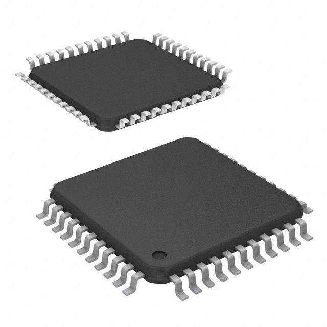
| 描述 | IC 80C51 MCU 8BIT ROMLESS 44PLCC8位微控制器 -MCU 8B MCU128/256B RAM 2.7-5.5V 33MHZ |
| EEPROM容量 | - |
| 产品分类 | |
| I/O数 | 32 |
| 品牌 | NXP Semiconductors |
| 产品手册 | |
| 产品图片 |
|
| rohs | 符合RoHS无铅 / 符合限制有害物质指令(RoHS)规范要求 |
| 产品系列 | 嵌入式处理器和控制器,微控制器 - MCU,8位微控制器 -MCU,NXP Semiconductors P80C31SFAA,51280C |
| 数据手册 | |
| 产品型号 | P80C31SFAA,512 |
| RAM容量 | 128 x 8 |
| 产品种类 | 8位微控制器 -MCU |
| 供应商器件封装 | 44-PLCC(16.59x16.59) |
| 其它名称 | 568-11335-5 |
| 包装 | 管件 |
| 商标 | NXP Semiconductors |
| 外设 | POR |
| 安装风格 | SMD/SMT |
| 定时器数量 | 3 Timer |
| 封装 | Tube |
| 封装/外壳 | 44-LCC(J 形引线) |
| 封装/箱体 | PLCC-44 |
| 工作温度 | 0°C ~ 70°C |
| 工作电源电压 | 2.7 V to 5.5 V |
| 工厂包装数量 | 1300 |
| 振荡器类型 | 内部 |
| 数据RAM大小 | 128 B |
| 数据ROM大小 | 4 kB |
| 数据Rom类型 | EEPROM |
| 数据总线宽度 | 8 bit |
| 数据转换器 | - |
| 最大工作温度 | + 85 C |
| 最大时钟频率 | 16 MHz |
| 最小工作温度 | - 40 C |
| 标准包装 | 26 |
| 核心 | 8051 |
| 核心处理器 | 8051 |
| 核心尺寸 | 8-位 |
| 片上ADC | No |
| 片上DAC | Without DAC |
| 电压-电源(Vcc/Vdd) | 2.7 V ~ 5.5 V |
| 电源电压-最大 | 5.5 V |
| 电源电压-最小 | 2.7 V |
| 程序存储器类型 | ROMless |
| 程序存储容量 | - |
| 连接性 | UART/USART |
| 速度 | 16MHz |


.jpg)


- 商务部:美国ITC正式对集成电路等产品启动337调查
- 曝三星4nm工艺存在良率问题 高通将骁龙8 Gen1或转产台积电
- 太阳诱电将投资9.5亿元在常州建新厂生产MLCC 预计2023年完工
- 英特尔发布欧洲新工厂建设计划 深化IDM 2.0 战略
- 台积电先进制程称霸业界 有大客户加持明年业绩稳了
- 达到5530亿美元!SIA预计今年全球半导体销售额将创下新高
- 英特尔拟将自动驾驶子公司Mobileye上市 估值或超500亿美元
- 三星加码芯片和SET,合并消费电子和移动部门,撤换高东真等 CEO
- 三星电子宣布重大人事变动 还合并消费电子和移动部门
- 海关总署:前11个月进口集成电路产品价值2.52万亿元 增长14.8%


PDF Datasheet 数据手册内容提取
INTEGRATED CIRCUITS 80C31/80C32 80C51 8-bit microcontroller family 128/256 byte RAM ROMless low voltage (2.7 V–5.5 V), low power, high speed (33 MHz) Product specification 2000 Aug 07 IC28 Data Handbook (cid:0)(cid:5)(cid:6)(cid:7)(cid:6)(cid:11)(cid:13) (cid:1)(cid:4)(cid:8)(cid:6)(cid:2)(cid:10)(cid:9)(cid:3)(cid:15)(cid:2)(cid:14)(cid:10)(cid:12)(cid:13)
Philips Semiconductors Product specification 80C51 8-bit microcontroller family 80C31/80C32 128/256 byte RAM ROMless low voltage (2.7V–5.5V), low power, high speed (33 MHz) DESCRIPTION FEATURES The Philips 80C31/32 is a high-performance static 80C51 design •8051 Central Processing Unit fabricated with Philips high-density CMOS technology with operation – 128 × 8 RAM (80C31) from 2.7 V to 5.5 V. – 256 × 8 RAM (80C32) The 80C31/32 ROMless devices contain a 128 × 8 RAM/256 ×8 – Three 16-bit counter/timers RAM, 32 I/O lines, three 16-bit counter/timers, a six-source, four-priority level nested interrupt structure, a serial I/O port for – Boolean processor either multi-processor communications, I/O expansion or full duplex – Full static operation UART, and on-chip oscillator and clock circuits. – Low voltage (2.7 V to 5.5 V@ 16 MHz) operation In addition, the device is a low power static design which offers a • Memory addressing capability wide range of operating frequencies down to zero. Two software – 64k ROM and 64k RAM selectable modes of power reduction—idle mode and power-down • mode are available. The idle mode freezes the CPU while allowing Power control modes: the RAM, timers, serial port, and interrupt system to continue – Clock can be stopped and resumed functioning. The power-down mode saves the RAM contents but – Idle mode freezes the oscillator, causing all other chip functions to be inoperative. Since the design is static, the clock can be stopped – Power-down mode without loss of user data and then the execution resumed from the • CMOS and TTL compatible point the clock was stopped. • TWO speed ranges at VCC = 5 V SELECTION TABLE – 0 to 16 MHz For applications requiring more ROM and RAM, see the 8XC54/58 – 0 to 33 MHz and 8XC51RA+/RB+/RC+/80C51RA+ data sheet. • Three package styles • ROM/EPROM RAM Size Programmable Hardware Extended temperature ranges Memory Size (X by 8) Timer Counter Watch Dog • (X by 8) (PCA) Timer Dual Data Pointers • 80C31/8XC51 4 level priority interrupt • 0K/4K 128 No No 6 interrupt sources • 80C32/8XC52/54/58 Four 8-bit I/O ports • 0K/8K/16K/32K 256 No No Full–duplex enhanced UART 80C51RA+/8XC51RA+/RB+/RC+ – Framing error detection – Automatic address recognition 0K/8K/16K/32K 512 Yes Yes • Programmable clock out 8XC51RD+ • Asynchronous port reset 64K 1024 Yes Yes • Low EMI (inhibit ALE) • Wake-up from Power Down by an external interrupt 2000 Aug 07 2 853–2213 24293
Philips Semiconductors Product specification 80C51 8-bit microcontroller family 80C31/80C32 128/256 byte RAM ROMless low voltage (2.7V–5.5V), low power, high speed (33 MHz) 80C51/87C51 AND 80C31 ORDERING INFORMATION TEMPERATURE RANGE °C VOLTAGE FREQ. DRAWING ROMless AND PACKAGE RANGE (MHz) NUMBER PP8800CC3311SSBBPPNN 00 ttoo ++7700, PPllaassttiicc DDuuaall IInn-lliinnee PPaacckkaaggee 22.77 VV ttoo 55.55 VV 00 ttoo 1166 SSOOTT112299-11 PP8800CC3311SSBBAAAA 00 ttoo ++7700, PPllaassttiicc LLeeaaddeedd CChhiipp CCaarrrriieerr 22.77 VV ttoo 55.55 VV 00 ttoo 1166 SSOOTT118877-22 PP8800CC3311SSBBBBBB 00 ttoo ++7700, PPllaassttiicc QQuuaadd FFllaatt PPaacckk 22.77 VV ttoo 55.55 VV 00 ttoo 1166 SSOOTT330077-22 PP8800CC3311SSFFPPNN –4400 ttoo ++8855, PPllaassttiicc DDuuaall IInn-lliinnee PPaacckkaaggee 22.77 VV ttoo 55.55 VV 00 ttoo 1166 SSOOTT112299-11 PP8800CC3311SSFFAAAA –4400 ttoo ++8855, PPllaassttiicc LLeeaaddeedd CChhiipp CCaarrrriieerr 22.77 VV ttoo 55.55 VV 00 ttoo 1166 SSOOTT118877-22 PP8800CC3311SSFFBBBB –4400 ttoo ++8855, PPllaassttiicc QQuuaadd FFllaatt PPaacckk 22.77 VV ttoo 55.55 VV 00 ttoo 1166 SSOOTT330077-22 PART NUMBER DERIVATION DEVICE NUMBER OPERATING FREQUENCY, MAX (S) TEMPERATURE RANGE (B) PACKAGE (AA) P80C31 S = 16 MHz B = 0(cid:0) to +70(cid:0)C AA = PLCC P80C32 U = 33 MHz F = –40(cid:0)C to +85(cid:0)C BB = PQFP PN = PDIP 80C32 ORDERING INFORMATION TEMPERATURE RANGE °C FREQ DRAWING ROMless AND PACKAGE MHz NUMBER P80C32SBPN 0 to +70, Plastic Dual In-line Package 16 SOT129-1 P80C32SBAA 0 to +70, Plastic Leaded Chip Carrier 16 SOT187-2 P80C32SBBB 0 to +70, Plastic Quad Flat Pack 16 SOT307-2 P80C32SFP N –40 to +85, Plastic Dual In-line Package 16 SOT129-1 P80C32SFA A –40 to +85, Plastic Leaded Chip Carrier 16 SOT187-2 P80C32SFB B –40 to +85, Plastic Quad Flat Pack 16 SOT307-2 P80C32UBAA 0 to +70, Plastic Leaded Chip Carrier 33 SOT187-2 P80C32UBPN 0 to +70, Plastic Dual In-line Package 33 SOT129-1 P80C32UBBB 0 to +70, Plastic Quad Flat Pack 33 SOT307-2 P80C32UFA A –40 to +85, Plastic Leaded Chip Carrier 33 SOT187-2 P80C32UFPN –40 to +85, Plastic Dual In-line Package 33 SOT129-1 P80C32UFBB –40 to +85, Plastic Quad Flat Pack 33 SOT307-2 2000 Aug 07 3
Philips Semiconductors Product specification 80C51 8-bit microcontroller family 80C31/80C32 128/256 byte RAM ROMless low voltage (2.7V–5.5V), low power, high speed (33 MHz) BLOCK DIAGRAM P0.0–P0.7 P2.0–P2.7 PORT 0 PORT 2 DRIVERS DRIVERS VCC VSS RAM ADDR RAM PORT 0 PORT 2 ROM/EPROM REGISTER LATCH LATCH 8 REGIBSTER ACC PSOTINATCEKR PROGRAM ADDRESS TMP2 TMP1 REGISTER BUFFER ALU SFRs PC PSW TIMERS INCRE- MENTER 8 16 PROGRAM COUNTER PSEN N ALE/PROG TIMING CTIOTER DPTR’S EARVPSPT COANNTDROL NSTRUREGIS MULTIPLE I PD PORT 1 PORT 3 LATCH LATCH OSCILLATOR PORT 1 PORT 3 DRIVERS DRIVERS XTAL1 XTAL2 P1.0–P1.7 P3.0–P3.7 SU00845 2000 Aug 07 4
Philips Semiconductors Product specification 80C51 8-bit microcontroller family 80C31/80C32 128/256 byte RAM ROMless low voltage (2.7V–5.5V), low power, high speed (33 MHz) LOGIC SYMBOL PLASTIC LEADED CHIP CARRIER PIN FUNCTIONS VCC VSS 6 1 40 XTAL1 7 39 0 ADDRESS AND T R DATA BUS O LCC P XTAL2 T2 17 29 T2EX RST T 1 18 28 EA/VPP OR PSEN P Pin Function Pin Function Pin Function S ALE/PROG 1 NIC* 16 P3.4/T0 31 P2.7/A15 ON RxD 2 P1.0/T2 17 P3.5/T1 32 PSEN DARY FUNCTIIINNTTTxTTD0101 PORT 3 PORT 2 ADDRESS BUS 34567 PPPPP11111.....12345/T2EX 1122289012 PPXXV33TTSAA..S67LL//WR21DR 3333334567 ANEPPLA00ICE../76V*//PAAPDD76 N WR 8 P1.6 23 NIC* 38 P0.5/AD5 CO RD 9 P1.7 24 P2.0/A8 39 P0.4/AD4 SE 10 RST 25 P2.1/A9 40 P0.3/AD3 SU00830 11 P3.0/RxD 26 P2.2/A10 41 P0.2/AD2 12 NIC* 27 P2.3/A11 42 P0.1/AD1 13 P3.1/TxD 28 P2.4/A12 43 P0.0/AD0 14 P3.2/INT0 29 P2.5/A13 44 VCC 15 P3.3/INT1 30 P2.6/A14 PIN CONFIGURATIONS * NO INTERNAL CONNECTION SU01062 T2/P1.0 1 40 VCC PLASTIC QUAD FLAT PACK T2EX/P1.1 2 39 P0.0/AD0 PIN FUNCTIONS P1.2 3 38 P0.1/AD1 44 34 P1.3 4 37 P0.2/AD2 P1.4 5 36 P0.3/AD3 1 33 P1.5 6 35 P0.4/AD4 P1.6 7 34 P0.5/AD5 PQFP P1.7 8 33 P0.6/AD6 11 23 RST 9 32 P0.7/AD7 RxD/P3.010 DUAL 31 EA/VPP IN-LINE TxD/P3.1 11 PACKAGE 30 ALE 12 22 Pin Function Pin Function Pin Function INT0/P3.2 12 29 PSEN 1 P1.5 16 VSS 31 P0.6/AD6 INT1/P3.3 13 28 P2.7/A15 2 P1.6 17 NIC* 32 P0.5/AD5 3 P1.7 18 P2.0/A8 33 P0.4/AD4 T0/P3.4 14 27 P2.6/A14 4 RST 19 P2.1/A9 34 P0.3/AD3 5 P3.0/RxD 20 P2.2/A10 35 P0.2/AD2 T1/P3.5 15 26 P2.5/A13 6 NIC* 21 P2.3/A11 36 P0.1/AD1 7 P3.1/TxD 22 P2.4/A12 37 P0.0/AD0 WR/P3.6 16 25 P2.4/A12 8 P3.2/INT0 23 P2.5/A13 38 VCC RD/P3.717 24 P2.3/A11 9 P3.3/INT1 24 P2.6/A14 39 NIC* 10 P3.4/T0 25 P2.7/A15 40 P1.0/T2 XTAL2 18 23 P2.2/A10 11 P3.5/T1 26 PSEN 41 P1.1/T2EX 12 P3.6/WR 27 ALE 42 P1.2 XTAL1 19 22 P2.1/A9 13 P3.7/RD 28 NIC* 43 P1.3 VSS 20 21 P2.0/A8 14 XTAL2 29 EA/VPP 44 P1.4 15 XTAL1 30 P0.7/AD7 SU01063 * NO INTERNAL CONNECTION SU01064 2000 Aug 07 5
Philips Semiconductors Product specification 80C51 8-bit microcontroller family 80C31/80C32 128/256 byte RAM ROMless low voltage (2.7V–5.5V), low power, high speed (33 MHz) PIN DESCRIPTIONS PIN NUMBER MNEMONIC DIP LCC QFP TYPE NAME AND FUNCTION VSS 20 22 16 I Ground: 0 V reference. VCC 40 44 38 I Power Supply: This is the power supply voltage for normal, idle, and power-down operation. P0.0–0.7 39–32 43–36 37–30 I/O Port 0: Port 0 is an open-drain, bidirectional I/O port with Schmitt trigger inputs. Port 0 pins that have 1s written to them float and can be used as high-impedance inputs. Port 0 is also the multiplexed low-order address and data bus during accesses to external program and data memory. In this application, it uses strong internal pull-ups when emitting 1s. P1.0–P1.7 1–8 2–9 40–44, I/O Port 1: Port 1 is an 8-bit bidirectional I/O port with internal pull-ups and Schmitt trigger 1–3 inputs. Port 1 pins that have 1s written to them are pulled high by the internal pull-ups and can be used as inputs. As inputs, port 1 pins that are externally pulled low will source current because of the internal pull-ups. (See DC Electrical Characteristics: IIL). Alternate functions for Port 1 include: 1 2 40 I/O T2 (P1.0): Timer/Counter 2 external count input/clockout (see Programmable Clock-Out) 2 3 41 I T2EX (P1.1): Timer/Counter 2 Reload/Capture/Direction control P2.0–P2.7 21–28 24–31 18–25 I/O Port 2: Port 2 is an 8-bit bidirectional I/O port with internal pull-ups and Schmitt trigger inputs. Port 2 pins that have 1s written to them are pulled high by the internal pull-ups and can be used as inputs. As inputs, port 2 pins that are externally being pulled low will source current because of the internal pull-ups. (See DC Electrical Characteristics: IIL). Port 2 emits the high-order address byte during fetches from external program memory and during accesses to external data memory that use 16-bit addresses (MOVX @DPTR). In this application, it uses strong internal pull-ups when emitting 1s. During accesses to external data memory that use 8-bit addresses (MOV @Ri), port 2 emits the contents of the P2 special function register. P3.0–P3.7 10–17 11, 5, I/O Port 3: Port 3 is an 8-bit bidirectional I/O port with internal pull-ups and Schmitt trigger 13–19 7–13 inputs. Port 3 pins that have 1s written to them are pulled high by the internal pull-ups and can be used as inputs. As inputs, port 3 pins that are externally being pulled low will source current because of the pull-ups. (See DC Electrical Characteristics: IIL). Port 3 also serves the special features of the 80C51 family, as listed below: 10 11 5 I RxD (P3.0): Serial input port 11 13 7 O TxD (P3.1): Serial output port 12 14 8 I INT0 (P3.2): External interrupt 13 15 9 I INT1 (P3.3): External interrupt 14 16 10 I T0 (P3.4): Timer 0 external input 15 17 11 I T1 (P3.5): Timer 1 external input 16 18 12 O WR (P3.6): External data memory write strobe 17 19 13 O RD (P3.7): External data memory read strobe RST 9 10 4 I Reset: A high on this pin for two machine cycles while the oscillator is running, resets the device. An internal diffused resistor to VSS permits a power-on reset using only an external capacitor to VCC. ALE 30 33 27 O Address Latch Enable: Output pulse for latching the low byte of the address during an access to external memory. In normal operation, ALE is emitted at a constant rate of 1/6 the oscillator frequency, and can be used for external timing or clocking. Note that one ALE pulse is skipped during each access to external data memory. ALE can be disabled by setting SFR auxiliary.0. With this bit set, ALE will be active only during a MOVX instruction. PSEN 29 32 26 O Program Store Enable: The read strobe to external program memory. When the 80C31/32 is executing code from the external program memory, PSEN is activated twice each machine cycle, except that two PSEN activations are skipped during each access to external data memory. PSEN is not activated during fetches from internal program memory. EA/VPP 31 35 29 I External Access Enable/Programming Supply Voltage: EA must be externally held low to enable the device to fetch code from external program memory locations 0000H to 0FFFH. XTAL1 19 21 15 I Crystal 1: Input to the inverting oscillator amplifier and input to the internal clock generator circuits. XTAL2 18 20 14 O Crystal 2: Output from the inverting oscillator amplifier. NOTE: To avoid “latch-up” effect at power-on, the voltage on any pin at any time must not be higher than VCC + 0.5 V or VSS – 0.5 V, respectively. 2000 Aug 07 6
Philips Semiconductors Product specification 80C51 8-bit microcontroller family 80C31/80C32 128/256 byte RAM ROMless low voltage (2.7V–5.5V), low power, high speed (33 MHz) Table 1. 8XC51/80C31 Special Function Registers DIRECT BIT ADDRESS, SYMBOL, OR ALTERNATIVE PORT FUNCTION RESET SYMBOL DESCRIPTION ADDRESS MSB LSB VALUE ACC* Accumulator E0H E7 E6 E5 E4 E3 E2 E1 E0 00H AUXR# Auxiliary 8EH – – – – – – – AO xxxxxxx0B AUXR1# Auxiliary 1 A2H – – – – WUPD2 0 – DPS xxx000x0B B* B register F0H F7 F6 F5 F4 F3 F2 F1 F0 00H DPTR: Data Pointer (2 bytes) DPH Data Pointer High 83H 00H DPL Data Pointer Low 82H 00H AF AE AD AC AB AA A9 A8 IE* Interrupt Enable A8H EA – ET2 ES ET1 EX1 ET0 EX0 0x000000B BF BE BD BC BB BA B9 B8 IP* Interrupt Priority B8H – – PT2 PS PT1 PX1 PT0 PX0 xx000000B B7 B6 B5 B4 B3 B2 B1 B0 IPH# Interrupt Priority High B7H – – PT2H PSH PT1H PX1H PT0H PX0H xx000000B 87 86 85 84 83 82 81 80 P0* Port 0 80H AD7 AD6 AD5 AD4 AD3 AD2 AD1 AD0 FFH 97 96 95 94 93 92 91 90 P1* Port 1 90H – – – – – – T2EX T2 FFH A7 A6 A5 A4 A3 A2 A1 A0 P2* Port 2 A0H AD15 AD14 AD13 AD12 AD11 AD10 AD9 AD8 FFH B7 B6 B5 B4 B3 B2 B1 B0 P3* Port 3 B0H RD WR T1 T0 INT1 INT0 TxD RxD FFH PCON#1 Power Control 87H SMOD1 SMOD0 – POF GF1 GF0 PD IDL 00xx0000B D7 D6 D5 D4 D3 D2 D1 D0 PSW* Program Status Word D0H CY AC F0 RS1 RS0 OV – P 000000x0B RACAP2H# Timer 2 Capture High CBH 00H RACAP2L# Timer 2 Capture Low CAH 00H SADDR# Slave Address A9H 00H SADEN# Slave Address Mask B9H 00H SBUF Serial Data Buffer 99H xxxxxxxxB 9F 9E 9D 9C 9B 9A 99 98 SCON* Serial Control 98H SM0/FE SM1 SM2 REN TB8 RB8 TI RI 00H SP Stack Pointer 81H 07H 8F 8E 8D 8C 8B 8A 89 88 TCON* Timer Control 88H TF1 TR1 TF0 TR0 IE1 IT1 IE0 IT0 00H CF CE CD CC CB CA C9 C8 T2CON* Timer 2 Control C8H TF2 EXF2 RCLK TCLK EXEN2 TR2 C/T2 CP/RL2 00H T2MOD# Timer 2 Mode Control C9H – – – – – – T2OE DCEN xxxxxx00B TH0 Timer High 0 8CH 00H TH1 Timer High 1 8DH 00H TH2# Timer High 2 CDH 00H TL0 Timer Low 0 8AH 00H TL1 Timer Low 1 8BH 00H TL2# Timer Low 2 CCH 00H TMOD Timer Mode 89H GATE C/T M1 M0 GATE C/T M1 M0 00H NOTE: Unused register bits that are not defined should not be set by the user’s program. If violated, the device could function incorrectly. * SFRs are bit addressable. # SFRs are modified from or added to the 80C51 SFRs. – Reserved bits. 1. Reset value depends on reset source. 2. Not available on 80C31. 2000 Aug 07 7
Philips Semiconductors Product specification 80C51 8-bit microcontroller family 80C31/80C32 128/256 byte RAM ROMless low voltage (2.7V–5.5V), low power, high speed (33 MHz) OSCILLATOR CHARACTERISTICS For the 80C31 or 80C32, either a hardware reset or external XTAL1 and XTAL2 are the input and output, respectively, of an interrupt can be used to exit from Power Down. Reset redefines all inverting amplifier. The pins can be configured for use as an on-chip the SFRs but does not change the on-chip RAM. An external oscillator, as shown in the logic symbol. interrupt allows both the SFRs and the on-chip RAM to retain their values. WUPD (AUXR1.3–Wakeup from Power Down) enables or To drive the device from an external clock source, XTAL1 should be disables the wakeup from power down with external interrupt. driven while XTAL2 is left unconnected. There are no requirements Where: on the duty cycle of the external clock signal, because the input to WUPD = 0 Disable the internal clock circuitry is through a divide-by-two flip-flop. WUPD = 1 Enable However, minimum and maximum high and low times specified in the data sheet must be observed. To properly terminate Power Down the reset or external interrupt should not be executed before VCC is restored to its normal Reset operating level and must be held active long enough for the A reset is accomplished by holding the RST pin high for at least two oscillator to restart and stabilize (normally less than 10 ms). machine cycles (24 oscillator periods), while the oscillator is running. With an external interrupt, INT0 or INT1 must be enabled and To insure a good power-up reset, the RST pin must be high long configured as level-sensitive. Holding the pin low restarts the enough to allow the oscillator time to start up (normally a few oscillator but bringing the pin back high completes the exit. Once the milliseconds) plus two machine cycles. interrupt is serviced, the next instruction to be executed after RETI Stop Clock Mode will be the one following the instruction that put the device into Power Down. The static design enables the clock speed to be reduced down to 0 MHz (stopped). When the oscillator is stopped, the RAM and For the 80C31, wakeup from power down is always enabled. Special Function Registers retain their values. This mode allows Design Consideration step-by-step utilization and permits reduced system power • consumption by lowering the clock frequency down to any value. For When the idle mode is terminated by a hardware reset, the device lowest power consumption the Power Down mode is suggested. normally resumes program execution, from where it left off, up to two machine cycles before the internal reset algorithm takes Idle Mode control. On-chip hardware inhibits access to internal RAM in this In idle mode (see Table 2), the CPU puts itself to sleep while all of event, but access to the port pins is not inhibited. To eliminate the the on-chip peripherals stay active. The instruction to invoke the idle possibility of an unexpected write when Idle is terminated by reset, mode is the last instruction executed in the normal operating mode the instruction following the one that invokes Idle should not be before the idle mode is activated. The CPU contents, the on-chip one that writes to a port pin or to external memory. RAM, and all of the special function registers remain intact during ONCE Mode this mode. The idle mode can be terminated either by any enabled interrupt (at which time the process is picked up at the interrupt The ONCE (“On-Circuit Emulation”) Mode facilitates testing and service routine and continued), or by a hardware reset which starts debugging of systems without the device having to be removed from the processor in the same manner as a power-on reset. the circuit. The ONCE Mode is invoked by: 1. Pull ALE low while the device is in reset and PSEN is high; Power-Down Mode 2. Hold ALE low as RST is deactivated. To save even more power, a Power Down mode (see Table 2) can be invoked by software. In this mode, the oscillator is stopped and While the device is in ONCE Mode, the Port 0 pins go into a float the instruction that invoked Power Down is the last instruction state, and the other port pins and ALE and PSEN are weakly pulled executed. The on-chip RAM and Special Function Registers retain high. The oscillator circuit remains active. While the 80C31/32 is in their values down to 2.0 V and care must be taken to return VCC to this mode, an emulator or test CPU can be used to drive the circuit. the minimum specified operating voltages before the Power Down Normal operation is restored when a normal reset is applied. Mode is terminated. Table 2. External Pin Status During Idle and Power-Down Modes MODE PROGRAM MEMORY ALE PSEN PORT 0 PORT 1 PORT 2 PORT 3 Idle Internal 1 1 Data Data Data Data Idle External 1 1 Float Data Address Data Power-down Internal 0 0 Data Data Data Data Power-down External 0 0 Float Data Data Data 2000 Aug 07 8
Philips Semiconductors Product specification 80C51 8-bit microcontroller family 80C31/80C32 128/256 byte RAM ROMless low voltage (2.7V–5.5V), low power, high speed (33 MHz) Programmable Clock-Out TH2, to be captured into registers RCAP2L and RCAP2H, A 50% duty cycle clock can be programmed to come out on P1.0. respectively. In addition, the transition at T2EX causes bit EXF2 in This pin, besides being a regular I/O pin, has two alternate T2CON to be set, and EXF2 like TF2 can generate an interrupt functions. It can be programmed: (which vectors to the same location as Timer 2 overflow interrupt. The Timer 2 interrupt service routine can interrogate TF2 and EXF2 1. to input the external clock for Timer/Counter 2, or to determine which event caused the interrupt). The capture mode is 2. to output a 50% duty cycle clock ranging from 61 Hz to 4 MHz at illustrated in Figure 2 (There is no reload value for TL2 and TH2 in a 16 MHz operating frequency. this mode. Even when a capture event occurs from T2EX, the To configure the Timer/Counter 2 as a clock generator, bit C/T2 (in counter keeps on counting T2EX pin transitions or osc/12 pulses.). T2CON) must be cleared and bit T20E in T2MOD must be set. Bit Auto-Reload Mode (Up or Down Counter) TR2 (T2CON.2) also must be set to start the timer. In the 16-bit auto-reload mode, Timer 2 can be configured (as either The Clock-Out frequency depends on the oscillator frequency and a timer or counter (C/T2* in T2CON)) then programmed to count up the reload value of Timer 2 capture registers (RCAP2H, RCAP2L) or down. The counting direction is determined by bit DCEN (Down as shown in this equation: Counter Enable) which is located in the T2MOD register (see Figure 3). When reset is applied the DCEN=0 which means Timer 2 Oscillator Frequency will default to counting up. If DCEN bit is set, Timer 2 can count up 4(cid:0)(65536(cid:1)RCAP2H,RCAP2L) or down depending on the value of the T2EX pin. Where: Figure 4 shows Timer 2 which will count up automatically since (RCAP2H,RCAP2L) = the content of RCAP2H and RCAP2L DCEN=0. In this mode there are two options selected by bit EXEN2 taken as a 16-bit unsigned integer. in T2CON register. If EXEN2=0, then Timer 2 counts up to 0FFFFH In the Clock-Out mode Timer 2 roll-overs will not generate an and sets the TF2 (Overflow Flag) bit upon overflow. This causes the interrupt. This is similar to when it is used as a baud-rate generator. Timer 2 registers to be reloaded with the 16-bit value in RCAP2L It is possible to use Timer 2 as a baud-rate generator and a clock and RCAP2H. The values in RCAP2L and RCAP2H are preset by generator simultaneously. Note, however, that the baud-rate and the software means. Clock-Out frequency will be the same. If EXEN2=1, then a 16-bit reload can be triggered either by an overflow or by a 1-to-0 transition at input T2EX. This transition also sets the EXF2 bit. The Timer 2 interrupt, if enabled, can be TIMER 2 OPERATION generated when either TF2 or EXF2 are 1. Timer 2 In Figure 5 DCEN=1 which enables Timer 2 to count up or down. Timer 2 is a 16-bit Timer/Counter which can operate as either an This mode allows pin T2EX to control the direction of count. When a event timer or an event counter, as selected by C/T2* in the special logic 1 is applied at pin T2EX Timer 2 will count up. Timer 2 will function register T2CON (see Figure 1). Timer 2 has three operating overflow at 0FFFFH and set the TF2 flag, which can then generate modes:Capture, Auto-reload (up or down counting) ,and Baud Rate an interrupt, if the interrupt is enabled. This timer overflow also Generator, which are selected by bits in the T2CON as shown in causes the 16–bit value in RCAP2L and RCAP2H to be reloaded Table 3. into the timer registers TL2 and TH2. When a logic 0 is applied at pin T2EX this causes Timer 2 to count Capture Mode down. The timer will underflow when TL2 and TH2 become equal to In the capture mode there are two options which are selected by bit the value stored in RCAP2L and RCAP2H. Timer 2 underflow sets EXEN2 in T2CON. If EXEN2=0, then timer 2 is a 16-bit timer or the TF2 flag and causes 0FFFFH to be reloaded into the timer counter (as selected by C/T2* in T2CON) which, upon overflowing registers TL2 and TH2. sets bit TF2, the timer 2 overflow bit. This bit can be used to generate an interrupt (by enabling the Timer 2 interrupt bit in the The external flag EXF2 toggles when Timer 2 underflows or IE register). If EXEN2= 1, Timer 2 operates as described above, but overflows. This EXF2 bit can be used as a 17th bit of resolution if with the added feature that a 1- to -0 transition at external input needed. The EXF2 flag does not generate an interrupt in this mode T2EX causes the current value in the Timer 2 registers, TL2 and of operation. Table 3. Timer 2 Operating Modes RCLK + TCLK CP/RL2 TR2 MODE 0 0 1 16-bit Auto-reload 0 1 1 16-bit Capture 1 X 1 Baud rate generator X X 0 (off) 2000 Aug 07 9
Philips Semiconductors Product specification 80C51 8-bit microcontroller family 80C31/80C32 128/256 byte RAM ROMless low voltage (2.7V–5.5V), low power, high speed (33 MHz) (MSB) (LSB) TF2 EXF2 RCLK TCLK EXEN2 TR2 C/T2 CP/RL2 Symbol Position Name and Significance TF2 T2CON.7 Timer 2 overflow flag set by a Timer 2 overflow and must be cleared by software. TF2 will not be set when either RCLK or TCLK = 1. EXF2 T2CON.6 Timer 2 external flag set when either a capture or reload is caused by a negative transition on T2EX and EXEN2 = 1. When Timer 2 interrupt is enabled, EXF2 = 1 will cause the CPU to vector to the Timer 2 interrupt routine. EXF2 must be cleared by software. EXF2 does not cause an interrupt in up/down counter mode (DCEN = 1). RCLK T2CON.5 Receive clock flag. When set, causes the serial port to use Timer 2 overflow pulses for its receive clock in modes 1 and 3. RCLK = 0 causes Timer 1 overflow to be used for the receive clock. TCLK T2CON.4 Transmit clock flag. When set, causes the serial port to use Timer 2 overflow pulses for its transmit clock in modes 1 and 3. TCLK = 0 causes Timer 1 overflows to be used for the transmit clock. EXEN2 T2CON.3 Timer 2 external enable flag. When set, allows a capture or reload to occur as a result of a negative transition on T2EX if Timer 2 is not being used to clock the serial port. EXEN2 = 0 causes Timer 2 to ignore events at T2EX. TR2 T2CON.2 Start/stop control for Timer 2. A logic 1 starts the timer. C/T2 T2CON.1 Timer or counter select. (Timer 2) 0 = Internal timer (OSC/12) 1 = External event counter (falling edge triggered). CP/RL2 T2CON.0 Capture/Reload flag. When set, captures will occur on negative transitions at T2EX if EXEN2 = 1. When cleared, auto-reloads will occur either with Timer 2 overflows or negative transitions at T2EX when EXEN2 = 1. When either RCLK = 1 or TCLK = 1, this bit is ignored and the timer is forced to auto-reload on Timer 2 overflow. SU00728 Figure 1. Timer/Counter 2 (T2CON) Control Register OSC ÷ 12 C/T2 = 0 TL2 TH2 TF2 (8-bits) (8-bits) C/T2 = 1 T2 Pin Control TR2 Capture Transition Timer 2 Detector Interrupt RCAP2L RCAP2H T2EX Pin EXF2 Control EXEN2 SU00066 Figure 2. Timer 2 in Capture Mode 2000 Aug 07 10
Philips Semiconductors Product specification 80C51 8-bit microcontroller family 80C31/80C32 128/256 byte RAM ROMless low voltage (2.7V–5.5V), low power, high speed (33 MHz) T2MOD Address = 0C9H Reset Value = XXXX XX00B Not Bit Addressable — — — — — — T2OE DCEN Bit 7 6 5 4 3 2 1 0 Symbol Function — Not implemented, reserved for future use.* T2OE Timer 2 Output Enable bit. DCEN Down Count Enable bit. When set, this allows Timer 2 to be configured as an up/down counter. * User software should not write 1s to reserved bits. These bits may be used in future 8051 family products to invoke new features. In that case, the reset or inactive value of the new bit will be 0, and its active value will be 1. The value read from a reserved bit is indeterminate. SU00729 Figure 3. Timer 2 Mode (T2MOD) Control Register OSC ÷ 12 C/T2 = 0 TL2 TH2 (8-BITS) (8-BITS) C/T2 = 1 T2 PIN CONTROL TR2 RELOAD TRANSITION DETECTOR RCAP2L RCAP2H TF2 TIMER 2 INTERRUPT T2EX PIN EXF2 CONTROL EXEN2 SU00067 Figure 4. Timer 2 in Auto-Reload Mode (DCEN = 0) 2000 Aug 07 11
Philips Semiconductors Product specification 80C51 8-bit microcontroller family 80C31/80C32 128/256 byte RAM ROMless low voltage (2.7V–5.5V), low power, high speed (33 MHz) (DOWN COUNTING RELOAD VALUE) FFH FFH TOGGLE EXF2 OSC ÷12 C/T2 = 0 OVERFLOW TL2 TH2 TF2 INTERRUPT T2 PIN C/T2 = 1 CONTROL TR2 COUNT DIRECTION 1 = UP 0 = DOWN RCAP2L RCAP2H (UP COUNTING RELOAD VALUE) T2EX PIN SU00730 Figure 5. Timer 2 Auto Reload Mode (DCEN = 1) Timer 1 Overflow NOTE: OSC. Freq. is divided by 2, not 12. ÷ 2 “0” “1” OSC ÷ 2 C/T2 = 0 SMOD TL2 TH2 “1” “0” (8-bits) (8-bits) RCLK C/T2 = 1 T2 Pin Control ÷ 16 RX Clock “1” “0” TR2 Reload TCLK Transition Detector RCAP2L RCAP2H ÷ 16 TX Clock T2EX Pin EXF2 Timer 2 Interrupt Control EXEN2 Note availability of additional external interrupt. SU00068 Figure 6. Timer 2 in Baud Rate Generator Mode 2000 Aug 07 12
Philips Semiconductors Product specification 80C51 8-bit microcontroller family 80C31/80C32 128/256 byte RAM ROMless low voltage (2.7V–5.5V), low power, high speed (33 MHz) Baud Rate Generator Mode under these conditions, a read or write of TH2 or TL2 may not be Bits TCLK and/or RCLK in T2CON (Table 3) allow the serial port accurate. The RCAP2 registers may be read, but should not be transmit and receive baud rates to be derived from either Timer 1 or written to, because a write might overlap a reload and cause write Timer 2. When TCLK= 0, Timer 1 is used as the serial port transmit and/or reload errors. The timer should be turned off (clear TR2) baud rate generator. When TCLK= 1, Timer 2 is used as the serial before accessing the Timer 2 or RCAP2 registers. port transmit baud rate generator. RCLK has the same effect for the Table 4 shows commonly used baud rates and how they can be serial port receive baud rate. With these two bits, the serial port can obtained from Timer 2. have different receive and transmit baud rates – one generated by Timer 1, the other by Timer 2. Table 4. Timer 2 Generated Commonly Used Figure 6 shows the Timer 2 in baud rate generation mode. The baud Baud Rates rate generation mode is like the auto-reload mode, in that a rollover in TH2 causes the Timer 2 registers to be reloaded with the 16-bit Timer 2 BBaaudd RRaattee OOsscc FFrreeqq value in registers RCAP2H and RCAP2L, which are preset by RCAP2H RCAP2L software. 375 K 12 MHz FF FF The baud rates in modes 1 and 3 are determined by Timer 2’s 9.6 K 12 MHz FF D9 overflow rate given below: 2.8 K 12 MHz FF B2 Modes 1 and 3 Baud Rates (cid:2) Timer 2 Overflow Rate 2.4 K 12 MHz FF 64 16 1.2 K 12 MHz FE C8 The timer can be configured for either “timer” or “counter” operation. 300 12 MHz FB 1E In many applications, it is configured for “timer” operation (C/T2*=0). 110 12 MHz F2 AF Timer operation is different for Timer 2 when it is being used as a 300 6 MHz FD 8F baud rate generator. 110 6 MHz F9 57 Usually, as a timer it would increment every machine cycle (i.e., 1/12 the oscillator frequency). As a baud rate generator, it increments Summary Of Baud Rate Equations every state time (i.e., 1/2 the oscillator frequency). Thus the baud Timer 2 is in baud rate generating mode. If Timer 2 is being clocked rate formula is as follows: through pin T2(P1.0) the baud rate is: Modes 1 and 3 Baud Rates = Baud Rate (cid:2) Timer 2 Overflow Rate 16 Oscillator Frequency [32(cid:0)[65536(cid:1)(RCAP2H,RCAP2L)]] If Timer 2 is being clocked internally, the baud rate is: Where: (RCAP2H, RCAP2L)= The content of RCAP2H and f Baud Rate(cid:2) OSC RCAP2L taken as a 16-bit unsigned integer. [32(cid:0)[65536(cid:1)(RCAP2H,RCAP2L)]] The Timer 2 as a baud rate generator mode shown in Figure 6, is Where fOSC= Oscillator Frequency valid only if RCLK and/or TCLK = 1 in T2CON register. Note that a To obtain the reload value for RCAP2H and RCAP2L, the above rollover in TH2 does not set TF2, and will not generate an interrupt. equation can be rewritten as: Thus, the Timer 2 interrupt does not have to be disabled when (cid:3) (cid:4) Timer 2 is in the baud rate generator mode. Also if the EXEN2 f (T2 external enable flag) is set, a 1-to-0 transition in T2EX RCAP2H,RCAP2L(cid:2)65536(cid:1) OSC 32(cid:0)Baud Rate (Timer/counter 2 trigger input) will set EXF2 (T2 external flag) but will not cause a reload from (RCAP2H, RCAP2L) to (TH2,TL2). Timer/Counter 2 Set-up Therefore when Timer 2 is in use as a baud rate generator, T2EX Except for the baud rate generator mode, the values given for can be used as an additional external interrupt, if needed. T2CON do not include the setting of the TR2 bit. Therefore, bit TR2 When Timer 2 is in the baud rate generator mode, one should not try must be set, separately, to turn the timer on. See Table 5 for set-up to read or write TH2 and TL2. As a baud rate generator, Timer 2 is of Timer 2 as a timer. Also see Table 6 for set-up of Timer 2 as a incremented every state time (osc/2) or asynchronously from pin T2; counter. 2000 Aug 07 13
Philips Semiconductors Product specification 80C51 8-bit microcontroller family 80C31/80C32 128/256 byte RAM ROMless low voltage (2.7V–5.5V), low power, high speed (33 MHz) Table 5. Timer 2 as a Timer T2CON MMOODDEE INTERNAL CONTROL (Note 1) EXTERNAL CONTROL (Note 2) 16-bit Auto-Reload 00H 08H 16-bit Capture 01H 09H Baud rate generator receive and transmit same baud rate 34H 36H Receive only 24H 26H Transmit only 14H 16H Table 6. Timer 2 as a Counter TMOD MMOODDEE INTERNAL CONTROL (Note 1) EXTERNAL CONTROL (Note 2) 16-bit 02H 0AH Auto-Reload 03H 0BH NOTES: 1. Capture/reload occurs only on timer/counter overflow. 2. Capture/reload occurs on timer/counter overflow and a 1-to-0 transition on T2EX (P1.1) pin except when Timer 2 is used in the baud rate generator mode. Enhanced UART SADDR are to b used and which bits are “don’t care”. The SADEN The UART operates in all of the usual modes that are described in mask can be logically ANDed with the SADDR to create the “Given” the first section of Data Handbook IC20, 80C51-Based 8-Bit address which the master will use for addressing each of the slaves. Microcontrollers. In addition the UART can perform framing error Use of the Given address allows multiple slaves to be recognized detect by looking for missing stop bits, and automatic address while excluding others. The following examples will help to show the recognition. The 80C31/32 UART also fully supports multiprocessor versatility of this scheme: communication. Slave 0 SADDR = 1100 0000 When used for framing error detect the UART looks for missing stop SADEN = 1111 1101 bits in the communication. A missing bit will set the FE bit in the Given = 1100 00X0 SCON register. The FE bit shares the SCON.7 bit with SM0 and the Slave 1 SADDR = 1100 0000 function of SCON.7 is determined by PCON.6 (SMOD0) (see SADEN = 1111 1110 Figure 7). If SMOD0 is set then SCON.7 functions as FE. SCON.7 Given = 1100 000X functions as SM0 when SMOD0 is cleared. When used as FE In the above example SADDR is the same and the SADEN data is SCON.7 can only be cleared by software. Refer to Figure 8. used to differentiate between the two slaves. Slave 0 requires a 0 in Automatic Address Recognition bit 0 and it ignores bit 1. Slave 1 requires a 0 in bit 1 and bit 0 is Automatic Address Recognition is a feature which allows the UART ignored. A unique address for Slave 0 would be 1100 0010 since to recognize certain addresses in the serial bit stream by using slave 1 requires a 0 in bit 1. A unique address for slave 1 would be hardware to make the comparisons. This feature saves a great deal 1100 0001 since a 1 in bit 0 will exclude slave 0. Both slaves can be of software overhead by eliminating the need for the software to selected at the same time by an address which has bit 0 = 0 (for examine every serial address which passes by the serial port. This slave 0) and bit 1 = 0 (for slave 1). Thus, both could be addressed feature is enabled by setting the SM2 bit in SCON. In the 9 bit UART with 1100 0000. modes, mode 2 and mode 3, the Receive Interrupt flag (RI) will be In a more complex system the following could be used to select automatically set when the received byte contains either the “Given” slaves 1 and 2 while excluding slave 0: address or the “Broadcast” address. The 9 bit mode requires that the 9th information bit is a 1 to indicate that the received information Slave 0 SADDR = 1100 0000 is an address and not data. Automatic address recognition is shown SADEN = 1111 1001 in Figure 9. Given = 1100 0XX0 The 8 bit mode is called Mode 1. In this mode the RI flag will be set Slave 1 SADDR = 1110 0000 if SM2 is enabled and the information received has a valid stop bit SADEN = 1111 1010 following the 8 address bits and the information is either a Given or Given = 1110 0X0X Broadcast address. Slave 2 SADDR = 1110 0000 Mode 0 is the Shift Register mode and SM2 is ignored. SADEN = 1111 1100 Given = 1110 00XX Using the Automatic Address Recognition feature allows a master to selectively communicate with one or more slaves by invoking the In the above example the differentiation among the 3 slaves is in the Given slave address or addresses. All of the slaves may be lower 3 address bits. Slave 0 requires that bit 0 = 0 and it can be contacted by using the Broadcast address. Two special Function uniquely addressed by 1110 0110. Slave 1 requires that bit 1 = 0 and Registers are used to define the slave’s address, SADDR, and the it can be uniquely addressed by 1110 and 0101. Slave 2 requires address mask, SADEN. SADEN is used to define which bits in the that bit 2 = 0 and its unique address is 1110 0011. To select Slaves 0 2000 Aug 07 14
Philips Semiconductors Product specification 80C51 8-bit microcontroller family 80C31/80C32 128/256 byte RAM ROMless low voltage (2.7V–5.5V), low power, high speed (33 MHz) and 1 and exclude Slave 2 use address 1110 0100, since it is Upon reset SADDR (SFR address 0A9H) and SADEN (SFR necessary to make bit 2 = 1 to exclude slave 2. address 0B9H) are leaded with 0s. This produces a given address of all “don’t cares” as well as a Broadcast address of all “don’t The Broadcast Address for each slave is created by taking the cares”. This effectively disables the Automatic Addressing mode and logical OR of SADDR and SADEN. Zeros in this result are trended allows the microcontroller to use standard 80C51 type UART drivers as don’t-cares. In most cases, interpreting the don’t-cares as ones, which do not make use of this feature. the broadcast address will be FF hexadecimal. SCON Address = 98H Reset Value = 0000 0000B Bit Addressable SM0/FE SM1 SM2 REN TB8 RB8 Tl Rl Bit: 7 6 5 4 3 2 1 0 (SMOD0 = 0/1)* Symbol Function FE Framing Error bit. This bit is set by the receiver when an invalid stop bit is detected. The FE bit is not cleared by valid frames but should be cleared by software. The SMOD0 bit must be set to enable access to the FE bit. SM0 Serial Port Mode Bit 0, (SMOD0 must = 0 to access bit SM0) SM1 Serial Port Mode Bit 1 SM0 SM1 Mode Description Baud Rate** 0 0 0 shift register fOSC/12 0 1 1 8-bit UART variable 1 0 2 9-bit UART fOSC/64 or fOSC/32 1 1 3 9-bit UART variable SM2 Enables the Automatic Address Recognition feature in Modes 2 or 3. If SM2 = 1 then Rl will not be set unless the received 9th data bit (RB8) is 1, indicating an address, and the received byte is a Given or Broadcast Address. In Mode 1, if SM2 = 1 then Rl will not be activated unless a valid stop bit was received, and the received byte is a Given or Broadcast Address. In Mode 0, SM2 should be 0. REN Enables serial reception. Set by software to enable reception. Clear by software to disable reception. TB8 The 9th data bit that will be transmitted in Modes 2 and 3. Set or clear by software as desired. RB8 In modes 2 and 3, the 9th data bit that was received. In Mode 1, if SM2 = 0, RB8 is the stop bit that was received. In Mode 0, RB8 is not used. Tl Transmit interrupt flag. Set by hardware at the end of the 8th bit time in Mode 0, or at the beginning of the stop bit in the other modes, in any serial transmission. Must be cleared by software. Rl Receive interrupt flag. Set by hardware at the end of the 8th bit time in Mode 0, or halfway through the stop bit time in the other modes, in any serial reception (except see SM2). Must be cleared by software. NOTE: *SMOD0 is located at PCON6. **fOSC = oscillator frequency SU00043 Figure 7. SCON: Serial Port Control Register 2000 Aug 07 15
Philips Semiconductors Product specification 80C51 8-bit microcontroller family 80C31/80C32 128/256 byte RAM ROMless low voltage (2.7V–5.5V), low power, high speed (33 MHz) D0 D1 D2 D3 D4 D5 D6 D7 D8 START DATA BYTE ONLY IN STOP BIT MODE 2, 3 BIT SET FE BIT IF STOP BIT IS 0 (FRAMING ERROR) SM0 TO UART MODE CONTROL SCON SM0 / FE SM1 SM2 REN TB8 RB8 TI RI (98H) PCON SMOD1 SMOD0 – POF GF1 GF0 PD IDL (87H) 0 : SCON.7 = SM0 1 : SCON.7 = FE SU01191 Figure 8. UART Framing Error Detection D0 D1 D2 D3 D4 D5 D6 D7 D8 SCON SM0 SM1 SM2 REN TB8 RB8 TI RI (98H) 1 1 1 1 X 1 0 RECEIVED ADDRESS D0 TO D7 COMPARATOR PROGRAMMED ADDRESS IN UART MODE 2 OR MODE 3 AND SM2 = 1: INTERRUPT IF REN=1, RB8=1 AND “RECEIVED ADDRESS” = “PROGRAMMED ADDRESS” – WHEN OWN ADDRESS RECEIVED, CLEAR SM2 TO RECEIVE DATA BYTES – WHEN ALL DATA BYTES HAVE BEEN RECEIVED: SET SM2 TO WAIT FOR NEXT ADDRESS. SU00045 Figure 9. UART Multiprocessor Communication, Automatic Address Recognition 2000 Aug 07 16
Philips Semiconductors Product specification 80C51 8-bit microcontroller family 80C31/80C32 128/256 byte RAM ROMless low voltage (2.7V–5.5V), low power, high speed (33 MHz) Interrupt Priority Structure An interrupt will be serviced as long as an interrupt of equal or The 80C31 and 80C32 have a 6-source four-level interrupt higher priority is not already being serviced. If an interrupt of equal structure. They are the IE, IP and IPH. (See Figures 10, 11, and 12.) or higher level priority is being serviced, the new interrupt will wait The IPH (Interrupt Priority High) register that makes the four-level until it is finished before being serviced. If a lower priority level interrupt structure possible. The IPH is located at SFR address B7H. interrupt is being serviced, it will be stopped and the new interrupt The structure of the IPH register and a description of its bits is serviced. When the new interrupt is finished, the lower priority level shown in Figure 12. interrupt that was stopped will be completed. The function of the IPH SFR is simple and when combined with the IP SFR determines the priority of each interrupt. The priority of each interrupt is determined as shown in the following table: PRIORITY BITS IINNTTEERRRRUUPPTT PPRRIIOORRIITTYY LLEEVVEELL IPH.x IP.x 0 0 Level 0 (lowest priority) 0 1 Level 1 1 0 Level 2 1 1 Level 3 (highest priority) Table 7. Interrupt Table SOURCE POLLING PRIORITY REQUEST BITS HARDWARE CLEAR? VECTOR ADDRESS X0 1 IE0 N (L)1 Y (T)2 03H T0 2 TP0 Y 0BH X1 3 IE1 N (L) Y (T) 13H T1 4 TF1 Y 1BH SP 5 RI, TI N 23H T2 6 TF2, EXF2 N 2BH NOTES: 1. L = Level activated 2. T = Transition activated 7 6 5 4 3 2 1 0 IE (0A8H) EA — ET2 ES ET1 EX1 ET0 EX0 Enable Bit = 1 enables the interrupt. Enable Bit = 0 disables it. BIT SYMBOL FUNCTION IE.7 EA Global disable bit. If EA = 0, all interrupts are disabled. If EA = 1, each interrupt can be individually enabled or disabled by setting or clearing its enable bit. IE.6 — Not implemented. Reserved for future use. IE.5 ET2 Timer 2 interrupt enable bit. IE.4 ES Serial Port interrupt enable bit. IE.3 ET1 Timer 1 interrupt enable bit. IE.2 EX1 External interrupt 1 enable bit. IE.1 ET0 Timer 0 interrupt enable bit. IE.0 EX0 External interrupt 0 enable bit. SU00571 Figure 10. IE Registers 2000 Aug 07 17
Philips Semiconductors Product specification 80C51 8-bit microcontroller family 80C31/80C32 128/256 byte RAM ROMless low voltage (2.7V–5.5V), low power, high speed (33 MHz) 7 6 5 4 3 2 1 0 IP (0B8H) — — PT2 PS PT1 PX1 PT0 PX0 Priority Bit = 1 assigns higher priority Priority Bit = 0 assigns lower priority BIT SYMBOL FUNCTION IP.7 — Not implemented, reserved for future use. IP.6 — Not implemented, reserved for future use. IP.5 PT2 Timer 2 interrupt priority bit. IP.4 PS Serial Port interrupt priority bit. IP.3 PT1 Timer 1 interrupt priority bit. IP.2 PX1 External interrupt 1 priority bit. IP.1 PT0 Timer 0 interrupt priority bit. IP.0 PX0 External interrupt 0 priority bit. SU00572 Figure 11. IP Registers 7 6 5 4 3 2 1 0 IPH (B7H) — — PT2H PSH PT1H PX1H PT0H PX0H Priority Bit = 1 assigns higher priority Priority Bit = 0 assigns lower priority BIT SYMBOL FUNCTION IPH.7 — Not implemented, reserved for future use. IPH.6 — Not implemented, reserved for future use. IPH.5 PT2H Timer 2 interrupt priority bit high. IPH.4 PSH Serial Port interrupt priority bit high. IPH.3 PT1H Timer 1 interrupt priority bit high. IPH.2 PX1H External interrupt 1 priority bit high. IPH.1 PT0H Timer 0 interrupt priority bit high. IPH.0 PX0H External interrupt 0 priority bit high. SU01058 Figure 12. IPH Registers 2000 Aug 07 18
Philips Semiconductors Product specification 80C51 8-bit microcontroller family 80C31/80C32 128/256 byte RAM ROMless low voltage (2.7V–5.5V), low power, high speed (33 MHz) Reduced EMI Mode Note that bit 2 is not writable and is always read as a zero. This The AO bit (AUXR.0) in the AUXR register when set disables the allows the DPS bit to be quickly toggled simply by executing an INC ALE output. DPTR instruction without affecting the WOPD or LPEP bits. Reduced EMI Mode AUXR (8EH) DPS 7 6 5 4 3 2 1 0 BIT0 – – – – – – – AO AUXR1 DPTR1 DPTR0 AUXR.0 AO Turns off ALE output. DPH DPL (83H) (82H) EXTERNAL DATA MEMORY Dual DPTR SU00745A The dual DPTR structure (see Figure 13) enables a way to specify the address of an external data memory location. There are two Figure 13. 16-bit DPTR registers that address the external memory, and a single bit called DPS = AUXR1/bit0 that allows the program code to switch between them. DPTR Instructions • The instructions that refer to DPTR refer to the data pointer that is New Register Name: AUXR1# currently selected using the AUXR1/bit 0 register. The six • SFR Address: A2H instructions that use the DPTR are as follows: • Reset Value: xxx000x0B INC DPTR Increments the data pointer by 1 AUXR1 (A2H) MOV DPTR, #data16 Loads the DPTR with a 16-bit constant 7 6 5 4 3 2 1 0 MOV A, @ A+DPTR Move code byte relative to DPTR to ACC – – – – WUPD 0 – DPS MOVX A, @ DPTR Move external RAM (16-bit address) to Where: ACC DPS = AUXR1/bit0 = Switches between DPTR0 and DPTR1. MOVX @ DPTR , A Move ACC to external RAM (16-bit address) Select Reg DPS DPTR0 0 JMP @ A + DPTR Jump indirect relative to DPTR DPTR1 1 The data pointer can be accessed on a byte-by-byte basis by specifying the low or high byte in an instruction which accesses the The DPS bit status should be saved by software when switching SFRs. See application note AN458 for more details. between DPTR0 and DPTR1. 2000 Aug 07 19
Philips Semiconductors Product specification 80C51 8-bit microcontroller family 80C31/80C32 128/256 byte RAM ROMless low voltage (2.7V–5.5V), low power, high speed (33 MHz) ABSOLUTE MAXIMUM RATINGS1, 2, 3 PARAMETER RATING UNIT Operating temperature under bias 0 to +70 or –40 to +85 °C Storage temperature range –65 to +150 °C Voltage on EA pin to VSS 0 to +13.0 V Voltage on any other pin to VSS –0.5 to +6.5 V Maximum IOL per I/O pin 15 mA Power dissipation (based on package heat transfer limitations, not device power consumption) 1.5 W NOTES: 1. Stresses above those listed under Absolute Maximum Ratings may cause permanent damage to the device. This is a stress rating only and functional operation of the device at these or any conditions other than those described in the AC and DC Electrical Characteristics section of this specification is not implied. 2. This product includes circuitry specifically designed for the protection of its internal devices from the damaging effects of excessive static charge. Nonetheless, it is suggested that conventional precautions be taken to avoid applying greater than the rated maximum. 3. Parameters are valid over operating temperature range unless otherwise specified. All voltages are with respect to VSS unless otherwise noted. AC ELECTRICAL CHARACTERISTICS Tamb = 0°C to +70°C or –40°C to +85°C CLOCK FREQUENCY RANGE –f SYMBOL FIGURE PARAMETER MIN MAX UNIT 1/tCLCL 29 Oscillator frequency Speed versions :S (16 MHz) 0 16 MHz U (33 MHz) 0 33 MHz 2000 Aug 07 20
Philips Semiconductors Product specification 80C51 8-bit microcontroller family 80C31/80C32 128/256 byte RAM ROMless low voltage (2.7V–5.5V), low power, high speed (33 MHz) DC ELECTRICAL CHARACTERISTICS Tamb = 0°C to +70°C or –40°C to +85°C, VCC = 2.7 V to 5.5 V, VSS = 0 V (16 MHz devices) TEST LIMITS SSYYMMBBOOLL PPAARRAAMMEETTEERR UUNNIITT CONDITIONS MIN TYP1 MAX 4.0 V < VCC < 5.5 V –0.5 0.2 VCC–0.1 V VVIL IInnppuutt llooww vvoollttaaggee 2.7 V<VCC< 4.0 V –0.5 0.7 V VIH Input high voltage (ports 0, 1, 2, 3, EA) 0.2 VCC+0.9 VCC+0.5 V VIH1 Input high voltage, XTAL1, RST 0.7 VCC VCC+0.5 V VOL Output low voltage, ports 1, 2, 8 IOVLC =C 1=. 62 .m7 AV2 0.4 V VOL1 Output low voltage, port 0, ALE, PSEN8, 7 IOVLC =C 3=. 22 .m7 AV2 0.4 V IVOHC C= =– 220.7 m VA VCC – 0.7 V VVOOH OOuuttppuutt hhiigghh vvoollttaaggee, ppoorrttss 11, 22, 3333 IVOHC C= =– 340.5 m VA VCC – 0.7 V VOH1 Omuotdpeu)t, AhLigEh9 ,v PoSltaEgNe3 (port 0 in external bus IOVHC =C –=3 2.2.7 m VA VCC – 0.7 V IIL Logical 0 input current, ports 1, 2, 3 VIN = 0.4 V –1 –50 m A ITL Logical 1-to-0 transition current, ports 1, 2, 36 VSIeNe = n 2o.t0e V4 –650 m A ILI Input leakage current, port 0 0.45 < VIN < VCC – 0.3 ±10 m A ICC Power supply current (see Figure 21): See note 5 Active mode @ 16 MHz m A Idle mode @ 16 MHz m A Power-down mode or clock stopped (see Tamb = 0°C to 70°C 3 50 m A FFiigure 2255 ffor conddiittiions)) Tamb = –40°C to +85°C 75 m A RRST Internal reset pull-down resistor 40 225 kW CIO Pin capacitance10 (except EA) 15 pF NOTES: 1. Typical ratings are not guaranteed. The values listed are at room temperature, 5 V. 2. Capacitive loading on ports 0 and 2 may cause spurious noise to be superimposed on the VOLs of ALE and ports 1 and 3. The noise is due to external bus capacitance discharging into the port 0 and port 2 pins when these pins make 1-to-0 transitions during bus operations. In the worst cases (capacitive loading > 100 pF), the noise pulse on the ALE pin may exceed 0.8 V. In such cases, it may be desirable to qualify ALE with a Schmitt Trigger, or use an address latch with a Schmitt Trigger STROBE input. IOL can exceed these conditions provided that no single output sinks more than 5 mA and no more than two outputs exceed the test conditions. 3. Capacitive loading on ports 0 and 2 may cause the VOH on ALE and PSEN to momentarily fall below the VCC–0.7 specification when the address bits are stabilizing. 4. Pins of ports 1, 2 and 3 source a transition current when they are being externally driven from 1 to 0. The transition current reaches its maximum value when VIN is approximately 2 V. 5. See Figures 22 through 25 for ICC test conditions. Active mode: ICC = 0.9 × FREQ. + 1.1 mA Idle mode: ICC = 0.18 × FREQ. +1.01 mA; See Figure 21. 6. This value applies to Tamb = 0°C to +70°C. For Tamb = –40°C to +85°C, ITL = –750 m A. 7. Load capacitance for port 0, ALE, and PSEN = 100 pF, load capacitance for all other outputs = 80 pF. 8. Under steady state (non-transient) conditions, IOL must be externally limited as follows: Maximum IOL per port pin: 15 mA (*NOTE: This is 85°C specification.) Maximum IOL per 8-bit port: 26 mA Maximum total IOL for all outputs: 71 mA If IOL exceeds the test condition, VOL may exceed the related specification. Pins are not guaranteed to sink current greater than the listed test conditions. 9. ALE is tested to VOH1, except when ALE is off then VOH is the voltage specification. 10.Pin capacitance is characterized but not tested. Pin capacitance is less than 25 pF. 2000 Aug 07 21
Philips Semiconductors Product specification 80C51 8-bit microcontroller family 80C31/80C32 128/256 byte RAM ROMless low voltage (2.7V–5.5V), low power, high speed (33 MHz) DC ELECTRICAL CHARACTERISTICS Tamb = 0°C to +70°C or –40°C to +85°C, 33 MHz devices; 5 V ±10%; VSS = 0 V LIMITS TEST SSYYMMBBOOLL PPAARRAAMMEETTEERR UUNNIITT CONDITIONS MIN TYP1 MAX VIL Input low voltage 4.5 V < VCC < 5.5 V –0.5 0.2 VCC–0.1 V VIH Input high voltage (ports 0, 1, 2, 3, EA) 0.2 VCC+0.9 VCC+0.5 V VIH1 Input high voltage, XTAL1, RST 0.7 VCC VCC+0.5 V VOL Output low voltage, ports 1, 2, 3 8 IVOLC C= =1 .46.m5 AV2 0.4 V VOL1 Output low voltage, port 0, ALE, PSEN7, 8 IVOLC C= =3 .42.m5 AV2 0.4 V VOH Output high voltage, ports 1, 2, 33 IVOCHC = = – 43.05m VA VCC – 0.7 V VOH1 Omuotdpeu)t, AhLigEh9 ,v PoSltaEgNe3 (port 0 in external bus IOVHC C= =– 34..25m VA VCC – 0.7 V IIL Logical 0 input current, ports 1, 2, 3 VIN = 0.4 V –1 –50 m A ITL Logical 1-to-0 transition current, ports 1, 2, 36 VSIeNe = n 2o.t0e V4 –650 m A ILI Input leakage current, port 0 0.45 < VIN < VCC – 0.3 ±10 m A ICC Power supply current (see Figure 21): See note 5 Active mode (see Note 5) Idle mode (see Note 5) Power-down mode or clock stopped (see Fig- Tamb = 0°C to 70°C 3 50 m A ure 2255 ffor conddiittiions)) Tamb = –40°C to +85°C 75 m A RRST Internal reset pull-down resistor 40 225 kW CIO Pin capacitance10 (except EA) 15 pF NOTES: 1. Typical ratings are not guaranteed. The values listed are at room temperature, 5 V. 2. Capacitive loading on ports 0 and 2 may cause spurious noise to be superimposed on the VOLs of ALE and ports 1 and 3. The noise is due to external bus capacitance discharging into the port 0 and port 2 pins when these pins make 1-to-0 transitions during bus operations. In the worst cases (capacitive loading > 100 pF), the noise pulse on the ALE pin may exceed 0.8 V. In such cases, it may be desirable to qualify ALE with a Schmitt Trigger, or use an address latch with a Schmitt Trigger STROBE input. IOL can exceed these conditions provided that no single output sinks more than 5mA and no more than two outputs exceed the test conditions. 3. Capacitive loading on ports 0 and 2 may cause the VOH on ALE and PSEN to momentarily fall below the VCC–0.7 specification when the address bits are stabilizing. 4. Pins of ports 1, 2 and 3 source a transition current when they are being externally driven from 1 to 0. The transition current reaches its maximum value when VIN is approximately 2 V. 5. See Figures 22 through 25 for ICC test conditions. Active mode: ICC(MAX) = 0.9 × FREQ. + 1.1 mA Idle mode: ICC(MAX) = 0.18 × FREQ. +1.0 mA; See Figure 21. 6. This value applies to Tamb = 0°C to +70°C. For Tamb = –40°C to +85°C, ITL = –750 m A. 7. Load capacitance for port 0, ALE, and PSEN = 100 pF, load capacitance for all other outputs = 80 pF. 8. Under steady state (non-transient) conditions, IOL must be externally limited as follows: Maximum IOL per port pin: 15 mA (*NOTE: This is 85°C specification.) Maximum IOL per 8-bit port: 26 mA Maximum total IOL for all outputs: 71 mA If IOL exceeds the test condition, VOL may exceed the related specification. Pins are not guaranteed to sink current greater than the listed test conditions. 9. ALE is tested to VOH1, except when ALE is off then VOH is the voltage specification. 10.Pin capacitance is characterized but not tested. Pin capacitance is less than 25 pF. Pin capacitance of ceramic package is less than 15 pF (except EA is 25 pF). 2000 Aug 07 22
Philips Semiconductors Product specification 80C51 8-bit microcontroller family 80C31/80C32 128/256 byte RAM ROMless low voltage (2.7V–5.5V), low power, high speed (33 MHz) AC ELECTRICAL CHARACTERISTICS Tamb = 0°C to +70°C or –40°C to +85°C, VCC = +2.7 V to +5.5 V, VSS = 0 V1, 2, 3 16 MHz CLOCK VARIABLE CLOCK SYMBOL FIGURE PARAMETER MIN MAX MIN MAX UNIT 1/tCLCL 14 Oscillator frequency5 Speed versions :S 3.5 16 MHz tLHLL 14 ALE pulse width 85 2tCLCL–40 ns tAVLL 14 Address valid to ALE low 22 tCLCL–40 ns tLLAX 14 Address hold after ALE low 32 tCLCL–30 ns tLLIV 14 ALE low to valid instruction in 150 4tCLCL–100 ns tLLPL 14 ALE low to PSEN low 32 tCLCL–30 ns tPLPH 14 PSEN pulse width 142 3tCLCL–45 ns tPLIV 14 PSEN low to valid instruction in 82 3tCLCL–105 ns tPXIX 14 Input instruction hold after PSEN 0 0 ns tPXIZ 14 Input instruction float after PSEN 37 tCLCL–25 ns tAVIV4 14 Address to valid instruction in 207 5tCLCL–105 ns tPLAZ 14 PSEN low to address float 10 10 ns Data Memory tRLRH 15, 16 RD pulse width 275 6tCLCL–100 ns tWLWH 15, 16 WR pulse width 275 6tCLCL–100 ns tRLDV 15, 16 RD low to valid data in 147 5tCLCL–165 ns tRHDX 15, 16 Data hold after RD 0 0 ns tRHDZ 15, 16 Data float after RD 65 2tCLCL–60 ns tLLDV 15, 16 ALE low to valid data in 350 8tCLCL–150 ns tAVDV 15, 16 Address to valid data in 397 9tCLCL–165 ns tLLWL 15, 16 ALE low to RD or WR low 137 239 3tCLCL–50 3tCLCL+50 ns tAVWL 15, 16 Address valid to WR low or RD low 122 4tCLCL–130 ns tQVWX 15, 16 Data valid to WR transition 13 tCLCL–50 ns tWHQX 15, 16 Data hold after WR 13 tCLCL–50 ns tQVWH 16 Data valid to WR high 287 7tCLCL–150 ns tRLAZ 15, 16 RD low to address float 0 0 ns tWHLH 15, 16 RD or WR high to ALE high 23 103 tCLCL–40 tCLCL+40 ns External Clock tCHCX 18 High time 20 20 tCLCL–tCLCX ns tCLCX 18 Low time 20 20 tCLCL–tCHCX ns tCLCH 18 Rise time 20 20 ns tCHCL 18 Fall time 20 20 ns Shift Register tXLXL 17 Serial port clock cycle time 750 12tCLCL ns tQVXH 17 Output data setup to clock rising edge 492 10tCLCL–133 ns tXHQX 17 Output data hold after clock rising edge 8 2tCLCL–117 ns tXHDX 17 Input data hold after clock rising edge 0 0 ns tXHDV 17 Clock rising edge to input data valid 492 10tCLCL–133 ns NOTES: 1. Parameters are valid over operating temperature range unless otherwise specified. 2. Load capacitance for port 0, ALE, and PSEN = 100 pF, load capacitance for all other outputs = 80 pF. 3. Interfacing the 80C31 and 80C32 to devices with float times up to 45ns is permitted. This limited bus contention will not cause damage to Port 0 drivers. 4. See application note AN457 for external memory interface. 5. Parts are guaranteed to operate down to 0 Hz. When an external clock source is used, the RST pin should be held high for a minimum of 20 m s for power-on or wakeup from power down. 2000 Aug 07 23
Philips Semiconductors Product specification 80C51 8-bit microcontroller family 80C31/80C32 128/256 byte RAM ROMless low voltage (2.7V–5.5V), low power, high speed (33 MHz) AC ELECTRICAL CHARACTERISTICS Tamb = 0°C to +70°C or –40°C to +85°C, VCC = 5 V ±10%, VSS = 0 V1, 2, 3 VARIABLE CLOCK4 16 MHz to fmax 33 MHz CLOCK SYMBOL FIGURE PARAMETER MIN MAX MIN MAX UNIT tLHLL 14 ALE pulse width 2tCLCL–40 21 ns tAVLL 14 Address valid to ALE low tCLCL–25 5 ns tLLAX 14 Address hold after ALE low tCLCL–25 ns tLLIV 14 ALE low to valid instruction in 4tCLCL–65 55 ns tLLPL 14 ALE low to PSEN low tCLCL–25 5 ns tPLPH 14 PSEN pulse width 3tCLCL–45 45 ns tPLIV 14 PSEN low to valid instruction in 3tCLCL–60 30 ns tPXIX 14 Input instruction hold after PSEN 0 0 ns tPXIZ 14 Input instruction float after PSEN tCLCL–25 5 ns tAVIV 14 Address to valid instruction in 5tCLCL–80 70 ns tPLAZ 14 PSEN low to address float 10 10 ns Data Memory tRLRH 15, 16 RD pulse width 6tCLCL–100 82 ns tWLWH 15, 16 WR pulse width 6tCLCL–100 82 ns tRLDV 15, 16 RD low to valid data in 5tCLCL–90 60 ns tRHDX 15, 16 Data hold after RD 0 0 ns tRHDZ 15, 16 Data float after RD 2tCLCL–28 32 ns tLLDV 15, 16 ALE low to valid data in 8tCLCL–150 90 ns tAVDV 15, 16 Address to valid data in 9tCLCL–165 105 ns tLLWL 15, 16 ALE low to RD or WR low 3tCLCL–50 3tCLCL+50 40 140 ns tAVWL 15, 16 Address valid to WR low or RD low 4tCLCL–75 45 ns tQVWX 15, 16 Data valid to WR transition tCLCL–30 0 ns tWHQX 15, 16 Data hold after WR tCLCL–25 5 ns tQVWH 16 Data valid to WR high 7tCLCL–130 80 ns tRLAZ 15, 16 RD low to address float 0 0 ns tWHLH 15, 16 RD or WR high to ALE high tCLCL–25 tCLCL+25 5 55 ns External Clock tCHCX 18 High time 0.38tCLCL tCLCL–tCLCX ns tCLCX 18 Low time 0.38tCLCL tCLCL–tCHCX ns tCLCH 18 Rise time 5 ns tCHCL 18 Fall time 5 ns Shift Register tXLXL 17 Serial port clock cycle time 12tCLCL 360 ns tQVXH 17 Output data setup to clock rising edge 10tCLCL–133 167 ns tXHQX 17 Output data hold after clock rising edge 2tCLCL–80 ns tXHDX 17 Input data hold after clock rising edge 0 0 ns tXHDV 17 Clock rising edge to input data valid 10tCLCL–133 167 ns NOTES: 1. Parameters are valid over operating temperature range unless otherwise specified. 2. Load capacitance for port 0, ALE, and PSEN = 100 pF, load capacitance for all other outputs = 80 pF. 3. Interfacing the 80C31 and 80C32 to devices with float times up to 45ns is permitted. This limited bus contention will not cause damage to Port 0 drivers. 4. Variable clock is specified for oscillator frequencies greater than 16 MHz to 33 MHz. For frequencies equal or less than 16 MHz, see 16 MHz “AC Electrical Characteristics”, page 23. 5. Parts are guaranteed to operate down to 0 Hz. When an external clock source is used, the RST pin should be held high for a minimum of 20 m s for power-on or wakeup from power down. 2000 Aug 07 24
Philips Semiconductors Product specification 80C51 8-bit microcontroller family 80C31/80C32 128/256 byte RAM ROMless low voltage (2.7V–5.5V), low power, high speed (33 MHz) EXPLANATION OF THE AC SYMBOLS Each timing symbol has five characters. The first character is always P – PSEN ‘t’ (= time). The other characters, depending on their positions, Q– Output data indicate the name of a signal or the logical status of that signal. The R– RD signal designations are: t – Time A – Address V – Valid C– Clock W– WR signal D– Input data X – No longer a valid logic level H– Logic level high Z – Float I – Instruction (program memory contents) Examples: tAVLL = Time for address valid to ALE low. L – Logic level low, or ALE tLLPL =Time for ALE low to PSEN low. tLHLL ALE tAVLL tLLPL tPLPH tLLIV PSEN tPLIV tLLAX tPLAZ tPXIZ tPXIX PORT 0 A0–A7 INSTR IN A0–A7 tAVIV PORT 2 A0–A15 A8–A15 SU00006 Figure 14. External Program Memory Read Cycle ALE tWHLH PSEN tLLDV tLLWL tRLRH RD tLLAX tRHDZ tAVLL tRLDV tRLAZ tRHDX PORT 0 FROMA R0I– OAR7 DPL DATA IN A0–A7 FROM PCL INSTR IN tAVWL tAVDV PORT 2 P2.0–P2.7 OR A8–A15 FROM DPF A0–A15 FROM PCH SU00025 Figure 15. External Data Memory Read Cycle 2000 Aug 07 25
Philips Semiconductors Product specification 80C51 8-bit microcontroller family 80C31/80C32 128/256 byte RAM ROMless low voltage (2.7V–5.5V), low power, high speed (33 MHz) ALE tWHLH PSEN tLLWL tWLWH WR tLLAX tAVLL tQVWX tWHQX tQVWH PORT 0 FROMA R0I– OAR7 DPL DATA OUT A0–A7 FROM PCL INSTR IN tAVWL PORT 2 P2.0–P2.7 OR A8–A15 FROM DPF A0–A15 FROM PCH SU00026 Figure 16. External Data Memory Write Cycle INSTRUCTION 0 1 2 3 4 5 6 7 8 ALE tXLXL CLOCK tXHQX tQVXH OUTPUT DATA 0 1 2 3 4 5 6 7 WRITE TO SBUF tXHDX tXHDV SET TI INPUT DATA VALID VALID VALID VALID VALID VALID VALID VALID CLEAR RI SET RI SU00027 Figure 17. Shift Register Mode Timing VCC–0.5 0.7VCC 0.45V 0.2VCC–0.1 tCHCX tCHCL tCLCX tCLCH tCLCL SU00009 Figure 18. External Clock Drive 2000 Aug 07 26
Philips Semiconductors Product specification 80C51 8-bit microcontroller family 80C31/80C32 128/256 byte RAM ROMless low voltage (2.7V–5.5V), low power, high speed (33 MHz) VCC–0.5 0.2VCC+0.9 VLOAD+0.1V TIMING VOH–0.1V VLOAD REFERENCE 0.45V 0.2VCC–0.1 VLOAD–0.1V POINTS VOL+0.1V NOTE: NOTE: AC inputs during testing are driven at VCC –0.5 for a logic ‘1’ and 0.45V for a logic ‘0’. For timing purposes, a port is no longer floating when a 100mV change from Timing measurements are made at VIH min for a logic ‘1’ and VIL max for a logic ‘0’. load voltage occurs, and begins to float when a 100mV change from the loaded VOH/VOL level occurs. IOH/IOL ≥ ±20mA. SU00717 SU00718 Figure 19. AC Testing Input/Output Figure 20. Float Waveform 35 30 25 MAX ACTIVE MODE mA) 20 (C ICCMAX = 0.9 X FREQ. + 1.1 C I 15 TYP ACTIVE MODE 10 MAX IDLE MODE 5 TYP IDLE MODE 4 8 12 16 20 24 28 32 36 FREQ AT XTAL1 (MHz) SU01413 Figure 21. ICC vs. FREQ Valid only within frequency specifications of the device under test 2000 Aug 07 27
Philips Semiconductors Product specification 80C51 8-bit microcontroller family 80C31/80C32 128/256 byte RAM ROMless low voltage (2.7V–5.5V), low power, high speed (33 MHz) VCC VCC ICC ICC VCC VCC VCC VCC RST VCC P0 P0 RST EA EA (NC) XTAL2 (NC) XTAL2 CLOCK SIGNAL XTAL1 CLOCK SIGNAL XTAL1 VSS VSS SU00719 SU00720 Figure 22. ICC Test Condition, Active Mode Figure 23. ICC Test Condition, Idle Mode All other pins are disconnected All other pins are disconnected VCC–0.5 0.7VCC 0.45V 0.2VCC–0.1 tCHCX tCHCL tCLCX tCLCH tCLCL SU00009 Figure 24. Clock Signal Waveform for ICC Tests in Active and Idle Modes tCLCH = tCHCL = 5ns VCC ICC VCC RST VCC P0 EA (NC) XTAL2 XTAL1 VSS SU00016 Figure 25. ICC Test Condition, Power Down Mode All other pins are disconnected. VCC = 2 V to 5.5 V 2000 Aug 07 28
Philips Semiconductors Product specification 80C51 8-bit microcontroller family 80C31/80C32 128/256 byte RAM ROMless low voltage (2.7V–5.5V), low power, high speed (33 MHz) DIP40: plastic dual in-line package; 40 leads (600 mil) SOT129-1 2000 Aug 07 29
Philips Semiconductors Product specification 80C51 8-bit microcontroller family 80C31/80C32 128/256 byte RAM ROMless low voltage (2.7V–5.5V), low power, high speed (33 MHz) PLCC44: plastic leaded chip carrier; 44 leads SOT187-2 2000 Aug 07 30
Philips Semiconductors Product specification 80C51 8-bit microcontroller family 80C31/80C32 128/256 byte RAM ROMless low voltage (2.7V–5.5V), low power, high speed (33 MHz) QFP44: plastic quad flat package; 44 leads (lead length 1.3 mm); body 10 x 10 x 1.75 mm SOT307-2 2000 Aug 07 31
Philips Semiconductors Product specification 80C51 8-bit microcontroller family 80C31/80C32 128/256 byte RAM ROMless low voltage (2.7V–5.5V), low power, high speed (33 MHz) Data sheet status Data sheet Product Definition [1] status status Objective Development This data sheet contains the design target or goal specifications for product development. specification Specification may change in any manner without notice. Preliminary Qualification This data sheet contains preliminary data, and supplementary data will be published at a later date. specification Philips Semiconductors reserves the right to make changes at any time without notice in order to improve design and supply the best possible product. Product Production This data sheet contains final specifications. Philips Semiconductors reserves the right to make specification changes at any time without notice in order to improve design and supply the best possible product. [1] Please consult the most recently issued datasheet before initiating or completing a design. Definitions Short-form specification — The data in a short-form specification is extracted from a full data sheet with the same type number and title. For detailed information see the relevant data sheet or data handbook. Limiting values definition — Limiting values given are in accordance with the Absolute Maximum Rating System (IEC 134). Stress above one or more of the limiting values may cause permanent damage to the device. These are stress ratings only and operation of the device at these or at any other conditions above those given in the Characteristics sections of the specification is not implied. Exposure to limiting values for extended periods may affect device reliability. Application information — Applications that are described herein for any of these products are for illustrative purposes only. Philips Semiconductors make no representation or warranty that such applications will be suitable for the specified use without further testing or modification. Disclaimers Life support — These products are not designed for use in life support appliances, devices or systems where malfunction of these products can reasonably be expected to result in personal injury. Philips Semiconductors customers using or selling these products for use in such applications do so at their own risk and agree to fully indemnify Philips Semiconductors for any damages resulting from such application. Right to make changes — Philips Semiconductors reserves the right to make changes, without notice, in the products, including circuits, standard cells, and/or software, described or contained herein in order to improve design and/or performance. Philips Semiconductors assumes no responsibility or liability for the use of any of these products, conveys no license or title under any patent, copyright, or mask work right to these products, and makes no representations or warranties that these products are free from patent, copyright, or mask work right infringement, unless otherwise specified. Philips Semiconductors Copyright Philips Electronics North America Corporation 2000 811 East Arques Avenue All rights reserved. Printed in U.S.A. P.O. Box 3409 Sunnyvale, California 94088–3409 Date of release: 08-00 Telephone 800-234-7381 Document order number: 9397 750 07403 (cid:0)(cid:5)(cid:6)(cid:7)(cid:6)(cid:11)(cid:13) (cid:1)(cid:4)(cid:8)(cid:6)(cid:2)(cid:10)(cid:9)(cid:3)(cid:15)(cid:2)(cid:14)(cid:10)(cid:12)(cid:13) 2000 Aug 07 32