 Datasheet下载
- 型号: P6KE200ARLG
- 制造商: ON Semiconductor
- 库位|库存: xxxx|xxxx
- 要求:
| 数量阶梯 | 香港交货 | 国内含税 |
| +xxxx | $xxxx | ¥xxxx |
查看当月历史价格
查看今年历史价格
P6KE200ARLG产品简介:
ICGOO电子元器件商城为您提供P6KE200ARLG由ON Semiconductor设计生产,在icgoo商城现货销售,并且可以通过原厂、代理商等渠道进行代购。 P6KE200ARLG价格参考¥1.27-¥1.27。ON SemiconductorP6KE200ARLG封装/规格:TVS - 二极管, 。您可以下载P6KE200ARLG参考资料、Datasheet数据手册功能说明书,资料中有P6KE200ARLG 详细功能的应用电路图电压和使用方法及教程。
Littelfuse Inc.的P6KE200ARLG是一款瞬态电压抑制(TVS)二极管,主要用于保护电路免受瞬态过电压事件(如雷击、静电放电和电源波动)的影响。它具有快速响应时间和低箝位电压特性,能够有效保护敏感电子设备。

 应用场景:

1. 通信设备:
   - 适用于各种通信接口(如RS-232、RS-485、以太网等),防止信号线上的瞬态电压损坏收发器。
   - 用于无线模块(如Wi-Fi、蓝牙、Zigbee等)的天线端口保护,确保数据传输的稳定性和可靠性。

2. 消费电子产品:
   - 在智能手机、平板电脑、笔记本电脑等便携式设备中,P6KE200ARLG可以保护USB端口、充电接口和耳机插孔等外部连接点。
   - 家用电器(如电视、音响系统、智能家居设备)中的电源输入和控制信号线也需要TVS二极管来抵御电压浪涌。

3. 工业自动化:
   - 工业控制系统中的传感器、执行器和其他I/O模块通常暴露在恶劣的电气环境中,P6KE200ARLG可以提供必要的保护,延长设备寿命并提高系统的稳定性。
   - 机器人和自动化生产线中的通信总线(如CAN、Profibus等)也需要TVS二极管来防止干扰和损坏。

4. 汽车电子:
   - 汽车内的各种电子控制单元(ECU)、传感器和通信网络(如LIN、CAN)需要可靠的过电压保护,以应对启动时的电压尖峰或电池短路等问题。
   - 车载娱乐系统、导航设备和安全系统(如ABS、ESP)同样依赖于TVS二极管来确保其正常工作。

5. 医疗设备:
   - 医疗仪器(如心电图机、超声波设备、监护仪等)对电气安全性要求极高,P6KE200ARLG可以保护这些设备的关键组件,确保患者和医护人员的安全。

总之,P6KE200ARLG TVS二极管广泛应用于各类电子设备中,特别是在那些需要高可靠性和长寿命的应用场合。它的快速响应特性和低箝位电压使其成为保护敏感电路的理想选择。
| 参数 | 数值 |
| 产品目录 | |
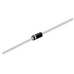
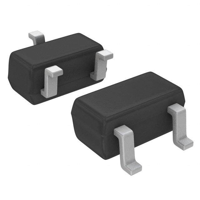
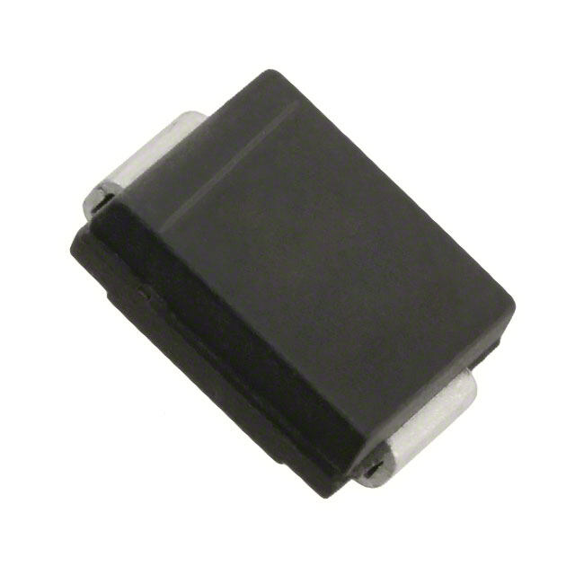
| 描述 | TVS DIODE 171VWM 274VC AXIALTVS 二极管 - 瞬态电压抑制器 200V 600W Unidirectional |
| 产品分类 | |
| 品牌 | ON Semiconductor |
| 产品手册 | |
| 产品图片 |
|
| rohs | 符合RoHS无铅 / 符合限制有害物质指令(RoHS)规范要求 |
| 产品系列 | 二极管与整流器,TVS二极管,TVS 二极管 - 瞬态电压抑制器,ON Semiconductor P6KE200ARLG- |
| 数据手册 | |
| 产品型号 | P6KE200ARLG |
| PCN设计/规格 | |
| 不同频率时的电容 | - |
| 产品种类 | TVS 二极管 - 瞬态电压抑制器 |
| 供应商器件封装 | 轴向 |
| 其它名称 | P6KE200ARLGOS |
| 击穿电压 | 190 V |
| 功率-峰值脉冲 | 600W |
| 包装 | 剪切带 (CT) |
| 单向通道 | 1 |
| 双向通道 | - |
| 商标 | ON Semiconductor |
| 安装类型 | 通孔 |
| 安装风格 | Through Hole |
| 封装 | Reel |
| 封装/外壳 | T-18,轴向 |
| 封装/箱体 | 017AA-01 |
| 尺寸 | 3.68 mm Dia. x 3.68 (Max) mm W x 8.89 mm L |
| 峰值浪涌电流 | 2.2 A |
| 峰值脉冲功率耗散 | 600 W |
| 工作温度 | -55°C ~ 150°C (TJ) |
| 工作电压 | 171 V |
| 工厂包装数量 | 4000 |
| 应用 | 通用 |
| 最大工作温度 | + 150 C |
| 最小工作温度 | - 55 C |
| 极性 | Unidirectional |
| 标准包装 | 1 |
| 电压-击穿(最小值) | 190V |
| 电压-反向关态(典型值) | 171V |
| 电压-箝位(最大值)@Ipp | 274V |
| 电流-峰值脉冲(10/1000µs) | 2.2A (8/20µs) |
| 电源线路保护 | 无 |
| 端接类型 | Axial |
| 类型 | 齐纳 |
| 系列 | P6KE6.8A |
| 钳位电压 | 274 V |


- 商务部:美国ITC正式对集成电路等产品启动337调查
- 曝三星4nm工艺存在良率问题 高通将骁龙8 Gen1或转产台积电
- 太阳诱电将投资9.5亿元在常州建新厂生产MLCC 预计2023年完工
- 英特尔发布欧洲新工厂建设计划 深化IDM 2.0 战略
- 台积电先进制程称霸业界 有大客户加持明年业绩稳了
- 达到5530亿美元!SIA预计今年全球半导体销售额将创下新高
- 英特尔拟将自动驾驶子公司Mobileye上市 估值或超500亿美元
- 三星加码芯片和SET,合并消费电子和移动部门,撤换高东真等 CEO
- 三星电子宣布重大人事变动 还合并消费电子和移动部门
- 海关总署:前11个月进口集成电路产品价值2.52万亿元 增长14.8%


PDF Datasheet 数据手册内容提取
P6KE6.8A Series 600 Watt Peak Power Littelfuse -40 Transient Voltage Suppressors Unidirectional* Littelfuse.com The P6KE6.8A series is designed to protect voltage sensitive components from high voltage, high energy transients. They have excellent clamping capability, high surge capability and fast response time. These devices are the Littelfuse exclusive, cost- effective, highly reliable axial leaded package and is ideally-suited for use in communication systems, numerical controls, process Cathode Anode controls, medical equipment, business machines, power supplies and many other industrial/consumer applications. Features: • Working Peak Reverse Voltage Range − 5.8 to 171 V • Peak Power − 600 W @ 1 ms • ESD Rating of Class 3 (>16 KV) per Human Body Model • Maximum Clamp Voltage @ Peak Pulse Current • Low Leakage < 5 (cid:2)A above 10 V AXIAL LEAD CASE 017AA • Maximum Temperature Coefficient Specified PLASTIC • UL 497B for Isolated Loop Circuit Protection • Response Time is Typically < 1 ns • Pb−Free Packages are Available MARKING DIAGRAM Mechanical Characteristics: CASE: Void-free, Transfer-molded, Thermosetting plastic FINISH: All external surfaces are corrosion resistant and leads are readily solderable A P6KE MAXIMUM LEAD TEMPERATURE FOR SOLDERING: xxxA 260(cid:3)C, 1/16″ from the case for 10 seconds YYWW(cid:4) (cid:4) POLARITY: Cathode indicated by polarity band MOUNTING POSITION: Any MAXIMUM RATINGS Rating Symbol Value Unit A = Assembly Location Peak Power Dissipation (Note 1) @ TL ≤ 25°C PPK 600 W P6KExxxA = Device Number YY = Year S@Dtee rTaaLdt ey≤d S2 a5tab°toCev, PeL oeTwaL de= rL 5De0ins°gsCtihp a=ti o3n/8 in PD 55.00 mWW/°C W(cid:4) W == PWbo−rFk rWeee ePkackage (Note: Microdot may be in either location) Thermal Resistance, Junction−to−Lead R(cid:3)JL 20 °C/W Forward Surge Current (Note 2) @ TA = 25°C IFSM 100 A ORDERING INFORMATION Operating and Storage Temperature Range TJ, Tstg −55 to °C +150 Device Package Shipping Stresses exceeding Maximum Ratings may damage the device. Maximum P6KExxxA Axial Lead 1000 Units / Box Ratings are stress ratings only. Functional operation above the Recommended P6KExxxAG Axial Lead 1000 Units / Box Operating Conditions is not implied. Extended exposure to stresses above the Recommended Operating Conditions may affect device reliability. (Pb−Free) 1. Nonrepetitive current pulse per Figure 4 and derated above TA = 25°C per P6KExxxARL Axial Lead 4000/Tape & Reel Figure 2. 2. 1/2 sine wave (or equivalent square wave), PW = 8.3 ms, duty cycle = 4 pulses P6KExxxARLG Axial Lead 4000/Tape & Reel per minute maximum. (Pb−Free) †For information on tape and reel specifications, including part orientation and tape sizes, please refer to our Tape and Reel Packaging Specifications Brochure, BRD8011/D. Specifications subject to change without notice. © 2016 Littelfuse, Inc. 1 Publication Order Number: September 19, 2016 − Rev. 10 P6KE6.8A/D
P6KE6.8A Series ELECTRICAL CHARACTERISTICS (TA = 25°C unless otherwise noted, VF = 3.5 V Max. @ IF (Note 6) = 50 A) I Symbol Parameter IF IPP Maximum Reverse Peak Pulse Current VC Clamping Voltage @ IPP VRWM Working Peak Reverse Voltage IR Maximum Reverse Leakage Current @ VRWM VCVBRVRWM IR VF V VBR Breakdown Voltage @ IT IT IT Test Current (cid:4)VBR Maximum Temperature Coefficient of VBR IF Forward Current IPP VF Forward Voltage @ IF Uni−Directional TVS ELECTRICAL CHARACTERISTICS (TA = 25°C unless otherwise noted, VF = 3.5 V Max. @ IF (Note 6) = 50 A) VRWM Breakdown Voltage VC @ IPP (Note 5) Device (Note 3) IR @ VRWM VBR (Note 4) (V) @ IT VC IPP (cid:2)VBR Device* Marking V (cid:2)A Min Nom Max mA V A %/°C P6KE6.8A, G P6KE6.8A 5.8 1000 6.45 6.80 7.14 10 10.5 57 0.057 P6KE7.5ARLG P6KE7.5A 6.4 500 7.13 7.51 7.88 10 11.3 53 0.061 P6KE10AG P6KE10A 8.55 10 9.5 10 10.5 1 14.5 41 0.073 P6KE12A, G P6KE12A 10.2 5 11.4 12 12.6 1 16.7 36 0.078 P6KE13AG P6KE13A 11.1 5 12.4 13.05 13.7 1 18.2 33 0.081 P6KE15AG P6KE15A 12.8 5 14.3 15.05 15.8 1 21.2 28 0.084 P6KE16A, G P6KE16A 13.6 5 15.2 16 16.8 1 22.5 27 0.086 P6KE18AG P6KE18A 15.3 5 17.1 18 18.9 1 25.2 24 0.088 P6KE20ARLG P6KE20A 17.1 5 19 20 21 1 27.7 22 0.09 P6KE22ARLG P6KE22A 18.8 5 20.9 22 23.1 1 30.6 20 0.092 P6KE24ARLG P6KE24A 20.5 5 22.8 24 25.2 1 33.2 18 0.094 P6KE27ARLG P6KE27A 23.1 5 25.7 27.05 28.4 1 37.5 16 0.096 P6KE30ARLG P6KE30A 25.6 5 28.5 30 31.5 1 41.4 14.4 0.097 P6KE33AG P6KE33A 28.2 5 31.4 33.05 34.7 1 45.7 13.2 0.098 P6KE36AG P6KE36A 30.8 5 34.2 36 37.8 1 49.9 12 0.099 P6KE39AG P6KE39A 33.3 5 37.1 39.05 41 1 53.9 11.2 0.1 P6KE43AG P6KE43A 36.8 5 40.9 43.05 45.2 1 59.3 10.1 0.101 P6KE47AG P6KE47A 40.2 5 44.7 47.05 49.4 1 64.8 9.3 0.101 P6KE51AG P6KE51A 43.6 5 48.5 51.05 53.6 1 70.1 8.6 0.102 P6KE56AG P6KE56A 47.8 5 53.2 56 58.8 1 77 7.8 0.103 P6KE62ARLG P6KE62A 53 5 58.9 62 65.1 1 85 7.1 0.104 P6KE68AG P6KE68A 58.1 5 64.6 68 71.4 1 92 6.5 0.104 P6KE75ARLG P6KE75A 64.1 5 71.3 75.05 78.8 1 103 5.8 0.105 P6KE82ARLG P6KE82A 70.1 5 77.9 82 86.1 1 113 5.3 0.105 P6KE91ARLG P6KE91A 77.8 5 86.5 91 95.5 1 125 4.8 0.106 P6KE100ARLG P6KE100A 85.5 5 95 100 105 1 137 4.4 0.106 P6KE120ARLG P6KE120A 102 5 114 120 126 1 165 3.6 0.107 P6KE130AG P6KE130A 111 5 124 130.5 137 1 179 3.3 0.107 P6KE150AG P6KE150A 128 5 143 150.5 158 1 207 2.9 0.108 P6KE160ARLG P6KE160A 136 5 152 160 168 1 219 2.7 0.108 P6KE180ARLG P6KE180A 154 5 171 180 189 1 246 2.4 0.108 P6KE200A, G P6KE200A 171 5 190 200 210 1 274 2.2 0.108 3. A transient suppressor is normally selected according to the maximum working peak reverse voltage (VRWM), which should be equal to or greater than the dc or continuous peak operating voltage level. 4. VBR measured at pulse test current IT at an ambient temperature of 25°C 5. Surge current waveform per Figure 4 and derate per Figures 1 and 2. 6. 1/2 sine wave (or equivalent square wave), PW = 8.3 ms, duty cycle = 4 pulses per minute maximum. *The “G’’ suffix indicates Pb−Free package or Pb−Free Packages are available. Specifications subject to change without notice. © 2016 Littelfuse, Inc. 2 Publication Order Number: September 19, 2016 − Rev. 10 P6KE6.8A/D
P6KE6.8A Series 100 C (cid:3) NONREPETITIVE PULSE F5 O2 WAVEFORM SHOWN IN % = W) FIGURE 4 N TA R (k10 NG IT @ 100 E TIN W AE P, PEAK POPK1 AK PULSE DERWER OR CURR 864000 EO 20 PP 0.1 K 0 0.1(cid:2)s 1(cid:2)s 10(cid:2)s 100(cid:2)s 1ms 10ms EA 0 25 50 75 100 125 150 175 200 P tP, PULSE WIDTH TA, AMBIENT TEMPERATURE ((cid:3)C) Figure 1. Pulse Rating Curve Figure 2. Pulse Derating Curve PULSE WIDTH (tp) IS tr ≤ 10(cid:2)s DEFINED AS THAT POINT WHERE THE pF)10,000 MEASURED @ %)100 PEAK VALUE − IPP PDEEACKA YCSU TROR E5N0%T OF IPP. E ( ZERO BIAS E ( TANC1000 VALU HALF VALUE − IP2P CI 50 A P MEASURED @ A 100 C, C VRWM tP 10 0 0.1 1 10 100 1000 0 1 2 3 4 VBR, BREAKDOWN VOLTAGE (VOLTS) t, TIME (ms) Figure 3. Capacitance versus Breakdown Voltage Figure 4. Pulse Waveform S) T T A W 1 N ( 0.7 O 3/8″ 0.5 TI A P 0.3 SSI 5 3/8″ OR 0.2 DI CT PULSE WIDTH ER 4 FA 0.1 10 ms W G O N0.07 TE P 3 RATI0.05 1 ms TA 2 DE0.03 Y S 0.02 100 (cid:2)s AD 1 10 (cid:2)s E 0.01 T 0 P, SD 0 25 5T0L, LE7A5D T1E0M0PE1R2A5TU1R5E0 (cid:3)C1)75 200 0.1 0.2 0.5 1 D, D2UTY CY5CLE (1%0) 20 50 100 Figure 5. Steady State Power Derating Figure 6. Typical Derating Factor for Duty Cycle Specifications subject to change without notice. © 2016 Littelfuse, Inc. 3 Publication Order Number: September 19, 2016 − Rev. 10 P6KE6.8A/D
P6KE6.8A Series APPLICATION NOTES RESPONSE TIME suppressor device as close as possible to the equipment or In most applications, the transient suppressor device is components to be protected will minimize this overshoot. placed in parallel with the equipment or component to be Some input impedance represented by Z is essential to in protected. In this situation, there is a time delay associated with prevent overstress of the protection device. This impedance the capacitance of the device and an overshoot condition should be as high as possible, without restricting the circuit associated with the inductance of the device and the inductance operation. of the connection method. The capacitance effect is of minor importance in the parallel protection scheme because it only DUTY CYCLE DERATING produces a time delay in the transition from the operating The data of Figure 1 applies for non-repetitive conditions voltage to the clamp voltage as shown in Figure 7. and at a lead temperature of 25°C. If the duty cycle increases, The inductive effects in the device are due to actual turn-on the peak power must be reduced as indicated by the curves of time (time required for the device to go from zero current to full Figure 6. Average power must be derated as the lead or ambient current) and lead inductance. This inductive effect produces an temperature rises above 25°C. The average power derating overshoot in the voltage across the equipment or component curve normally given on data sheets may be normalized and being protected as shown in Figure 8. Minimizing this used for this purpose. overshoot is very important in the application, since the main At first glance the derating curves of Figure 6 appear to be purpose for adding a transient suppressor is to clamp voltage in error as the 10 ms pulse has a higher derating factor than the spikes. The P6KE6.8A series has very good response time, 10 (cid:2)s pulse. However, when the derating factor for a given typically < 1 ns and negligible inductance. However, external pulse of Figure 6 is multiplied by the peak power value of inductive effects could produce unacceptable overshoot. Figure 1 for the same pulse, the results follow the expected Proper circuit layout, minimum lead lengths and placing the trend. TYPICAL PROTECTION CIRCUIT Zin Vin LOAD VL Vin (TRANSIENT) OVERSHOOT DUE TO V Vin (TRANSIENT) V INDUCTIVE EFFECTS VL VL Vin td tD = TIME DELAY DUE TO CAPACITIVE EFFECT t t Figure 7. Figure 8. UL RECOGNITION* The entire series including the bidirectional CA suffix has tests including Strike Voltage Breakdown test, Endurance Underwriters Laboratory Recognition for the classification of Conditioning, Temperature test, Dielectric Voltage-Withstand protectors (QVGQ2) under the UL standard for safety 497B test, Discharge test and several more. and File #E128662. Many competitors only have one or two Whereas, some competitors have only passed a flammability devices recognized or have recognition in a non-protective test for the package material, we have been recognized for category. Some competitors have no recognition at all. With much more to be included in their protector category. the UL497B recognition, our parts successfully passed several *Applies to P6KE6.8A − P6KE200A. Specifications subject to change without notice. © 2016 Littelfuse, Inc. 4 Publication Order Number: September 19, 2016 − Rev. 10 P6KE6.8A/D
P6KE6.8A Series PACKAGE DIMENSIONS LITTELFUSE 40, AXIAL LEAD CASE 017AA−01 ISSUE O NOTES: 1. CONTROLLING DIMENSION: INCH 2. LEAD DIAMETER AND FINISH NOT CONTROLLED WITHIN DIMENSION F. B 3. CATHODE BAND INDICATES POLARITY INCHES MILLIMETERS DIM MIN MAX MIN MAX D A 0.330 0.350 8.38 8.89 K B 0.130 0.145 3.30 3.68 D 0.037 0.043 0.94 1.09 F F --- 0.050 --- 1.27 K 1.000 1.250 25.40 31.75 A F K Littelfuse products are not designed for, and shall not be used for, any purpose (including, without limitation, automotive, military, aerospace, medical, life-saving, life-sustaining or nuclear facility applications, devices intended for surgical implant into the body, or any other application in which the failure or lack of desired operation of the product may result in personal injury, death, or property damage) other than those expressly set forth in applicable Littelfuse product documentation. Warranties granted by Littelfuse shall be deemed void for products used for any purpose not expressly set forth in applicable Littelfuse documentation. Littelfuse shall not be liable for any claims or damages arising out of products used in applications not expressly intended by Littelfuse as set forth in applicable Littelfuse documentation. The sale and use of Littelfuse products is subject to Littelfuse Terms and Conditions of Sale, unless otherwise agreed by Littelfuse. Littelfuse.com Specifications subject to change without notice. © 2016 Littelfuse, Inc. 5 Publication Order Number: September 19, 2016 − Rev. 10 P6KE6.8A/D