ICGOO在线商城 > P500-G120-WH
 Datasheet下载
- 型号: P500-G120-WH
- 制造商: Bourns
- 库位|库存: xxxx|xxxx
- 要求:
| 数量阶梯 | 香港交货 | 国内含税 |
| +xxxx | $xxxx | ¥xxxx |
查看当月历史价格
查看今年历史价格
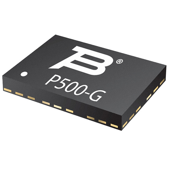
P500-G120-WH产品简介:
ICGOO电子元器件商城为您提供P500-G120-WH由Bourns设计生产,在icgoo商城现货销售,并且可以通过原厂、代理商等渠道进行代购。 提供P500-G120-WH价格参考¥4.41-¥11.85以及BournsP500-G120-WH封装/规格参数等产品信息。 你可以下载P500-G120-WH参考资料、Datasheet数据手册功能说明书, 资料中有P500-G120-WH详细功能的应用电路图电压和使用方法及教程。
| 参数 | 数值 |
| 产品目录 | |
| 描述 | SURGE SUPP TBU 100MA 500VIMP SMD浪涌抑制器 100mA 500Vimp |
| 产品分类 | |
| 品牌 | Bourns Inc. |
| 产品手册 | |
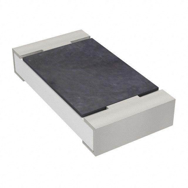
| 产品图片 |
|
| rohs | 符合RoHS无铅 / 符合限制有害物质指令(RoHS)规范要求 |
| 产品系列 | Bourns P500-G120-WHTBU® |
| 数据手册 | |
| 产品型号 | P500-G120-WH |
| PCN组件/产地 | |
| RoHS指令信息 | |
| 产品目录绘图 |
|
| 产品目录页面 | |
| 产品种类 | 浪涌抑制器 |
| 供应商器件封装 | 6-DFN(4x6) |
| 其它名称 | P500-G120-WHDKR |
| 功率(W) | - |
| 包装 | Digi-Reel® |
| 商标 | Bourns |
| 安装 | SMD/SMT |
| 宽度 | 4 mm |
| 封装 | Reel |
| 封装/外壳 | 6-SMD,无引线 |
| 工作温度范围 | - 40 C to + 85 C |
| 工厂包装数量 | 3000 |
| 应用 | SLIC |
| 技术 | 混合技术 |
| 标准包装 | 1 |
| 特色产品 | http://www.digikey.com/cn/zh/ph/Bourns/tbu.html |
| 电压-工作 | 300V |
| 电压-箝位 | - |
| 电压额定值 | 500 V |
| 电流额定值 | 120 mA |
| 电路数 | 2 |
| 端接类型 | SMD/SMT |
| 系列 | TBU |
| 长度 | 6 mm |
| 高度 | 0.85 mm |


- 商务部:美国ITC正式对集成电路等产品启动337调查
- 曝三星4nm工艺存在良率问题 高通将骁龙8 Gen1或转产台积电
- 太阳诱电将投资9.5亿元在常州建新厂生产MLCC 预计2023年完工
- 英特尔发布欧洲新工厂建设计划 深化IDM 2.0 战略
- 台积电先进制程称霸业界 有大客户加持明年业绩稳了
- 达到5530亿美元!SIA预计今年全球半导体销售额将创下新高
- 英特尔拟将自动驾驶子公司Mobileye上市 估值或超500亿美元
- 三星加码芯片和SET,合并消费电子和移动部门,撤换高东真等 CEO
- 三星电子宣布重大人事变动 还合并消费电子和移动部门
- 海关总署:前11个月进口集成电路产品价值2.52万亿元 增长14.8%
(B)(TU)-VG.jpg)


PDF Datasheet 数据手册内容提取
Features Applications NT MPLIA ■ Formerly brand ■ POTS linecards O HS C ■ Extremely high speed performance ■ VolP equipment *Ro ■ Blocks high voltages and currents ■ Voice and data combo linecards ■ Two TBU™ protectors in one small package ■ ONU, ONT ■ Simple, superior circuit protection ■ Gateways ■ Minimal PCB area ■ Cable and DSL modems ■ RoHS compliant*, UL Recognized TBU™ P500-G and P850-G Protectors Transient Blocking Units - TBU™ Devices Agency Approval Bourns® Model P500-G and P850-G UL recognized component File # E315805. TBU™ products are high speed, surge protection components designed to Industry Standards protect Subscriber Line Interface Circuits (SLICs) against transients caused by Description Model AC power cross, induction and lightning Port Type 2, 4 P500-G surges. Telcordia GR-1089 Port Type 3, 5 P850-G The TBU™ device blocks surges and ITU-T K.20, K.20E, K.21, K.21E, K.45 P850-G provides an effective barrier behind which sensitive electronics are not exposed to large voltages or currents during surge events. Absolute Maximum Ratings (T = 25 °C) amb Symbol Parameter Value Unit P500-Gxxx-WH 500 Vimp Maximum protection voltage for impulse faults with rise time ≥ 1 µsec P850-Gxxx-WH 850 V P500-Gxxx-WH 300 Vrms Maximum protection voltage for continuous Vrms faults P850-Gxxx-WH 425 V Top Operating temperature range -40 to +85 °C Tstg Storage temperature range -65 to +150 °C Electrical Characteristics (T = 25 °C) amb Symbol Parameter Min. Typ. Max. Unit P500-G120-WH 100 Maximum current through the device that will not cause P500-G200-WH 200 Iop current blocking P850-G120-WH 100 mA P850-G200-WH 200 P500-G120-WH 150 Typical current for the device to go from normal operating P500-G200-WH 275 Itrigger state to protected state P850-G120-WH 150 mA P850-G200-WH 275 P500-G120-WH 200 P500-G200-WH 400 Iout Maximum current through the device P850-G120-WH 200 mA P850-G200-WH 400 RTBU Series resistance of the TBU™ device 50 55 Ω Rbal Line-to line series resistance difference between two TBU™ devices 2 Ω Maximum time for the device to go from normal operating tblock state to protected state 1 µs Current through the triggered TBU™ device with 50 Vdc circuit Iquiescent voltage 0.7 mA Voltage below which the triggered TBU™ device will transition to Vreset normal operating state 22 V The P-G series TBU™ devices are bidirectional; specifi cations are valid in both directions. *RoHS Directive 2002/95/EC Jan 27 2003 including Annex. Specifi cations are subject to change without notice. Customers should verify actual device performance in their specifi c applications
TBU™ P500-G and P850-G Protectors Typical Performance Characteristics V-I Characteristics Time to Block vs. Fault Current +I 1 0.1 Itrigger c) 0.01 e s ( 0.001 k c o -Vreset Bl 0.0001 o +V t 0.00001 e m Ti 0.000001 Vreset 0.0000001 0.1 1 10 100 1000 Fault Current (A) -Itrigger Trigger Current Temperature 140 120 nt e r100 r u C r 80 e g g ri 60 T of % 40 20 -40 -20 0 20 40 60 80 Temperature (°C) Specifi cations are subject to change without notice. Customers should verify actual device performance in their specifi c applications
TBU™ P500-G and P850-G Protectors Operational Characteristics The graphs below demonstrate the operational characteristics of the TBU™ device. For each graph the fault voltage, protected side voltage, and current is presented. V1 V2 Tip nt e m TEST CONFIGURATION DIAGRAM Pxxx-G p ui q Ring E P500-G Lightning, 500 V P850-G Lightning, 850 V 3 3 100 V/div. 400 mA/div. 00 mA/div. 2 2 2 1 1 1 µs/div. 1 µs/div. Ch1 V1 Ch2 V2 Ch3 Current Ch1 V1 Ch2 V2 Ch3 Current P500-G Power Fault, 120 Vrms, 25 A P850-G Power Fault, 230 Vrms, 25 A 3 3 2 2 100 V/div. 200 mA/div. 100 V/div. 200 mA/div. 1 1 4 ms/div. 4 ms/div. Ch1 V1 Ch2 V2 Ch3 Current Ch1 V1 Ch2 V2 Ch3 Current Specifi cations are subject to change without notice. Customers should verify actual device performance in their specifi c applications
TBU™ P500-G and P850-G Protectors Product Dimensions P500-Gxxx K P500-G P850-G J K J Dim. Min. Typ. Max. Min. Typ. Max. B C E F E N 3.40 4.00 4.10 3.40 4.00 4.10 A (.139) (.157) (.161) (.139) (.157) (.161) 4 5 6 5.90 6.00 6.10 8.15 8.25 8.35 B (.232) (.236) (.240) (.321) (.325) (.329) A H 0.80 0.85 0.90 0.80 0.85 0.90 3 2 1 M C (.031) (.033) (.035) (.031) (.033) (.035) 0.000 0.025 0.050 0.000 0.025 0.050 D PIN 1 D N (.000) (.001) (.002) (.000) (.001) (.002) 1.15 1.25 1.35 1.15 1.25 1.35 E TOP VIEW SIDE VIEW BOTTOM VIEW (.045) (.049) (.053) (.045) (.049) (.053) 1.05 1.15 1.25 1.05 1.15 1.25 F P850-Gxxx K K (.041) (.045) (.049) (.041) (.045) (.049) J L L J G -- -- -- 0.725 0.825 0.925 B C G F G N (.029) (.032) (.036) E E 1.10 1.20 1.30 1.10 1.20 1.30 H 4A 4 5 6 6A (.043) (.047) (.051) (.043) (.047) (.051) 0.375 0.425 0.475 0.375 0.425 0.475 A H H J (.015) (.017) (.019) (.015) (.017) (.019) 3A 3 2 1 1A M 0.70 0.75 0.80 0.25 0.30 0.35 K (.028) (.030) (.031) (.010) (.012) (.014) 0.70 0.75 0.80 PIN 1 D N L -- -- -- (.028) (.030) (.031) TOP VIEW SIDE VIEW BOTTOM VIEW M 0.70 0.75 0.80 0.70 0.75 0.80 (.028) (.030) (.031) (.028) (.030) (.031) Pads 1A and 1 are internally connected; the same for pads 3A with 3, 4A with 4, and 6A with 6. 0.375 0.425 0.475 0.375 0.425 0.475 This allows for one PCB layout to accommodate the P500 or P850. N (.015) (.017) (.018) (.015) (.017) (.018) MM Recommended Pad Layout D IMENSIONS: (INCHES) P500-Gxxx Pad Designation 0.75 Pad # Apply Block Diagram (.030) 1.225 1 Tip In (.048) 1.275 1.15 P500-Gxxx (.050) (.045) 2 NC 3 Tip Out 4 Ring Out 6 4 5 NC 6 Ring In 0.375 (.015) NC = Solder to PCB; do not make electrical 1 3 connection, do not connect to ground. P850-Gxxx Pad Designation 0.85 1.25 1.225 (.033) (.049) 1.15 Pad # Apply Pad # Apply (.048) (.045) 1A Tip In 4A Ring Out 1 Tip In 4 Ring Out P850-Gxxx 2 NC 5 NC 3 Tip Out 6 Ring In 6&6A 4&4A 0.375 3A Tip Out 6A Ring In (.015) NC = Solder to PCB; do not make electrical 0.30 0.75 connection, do not connect to ground. (.012) (.030) 1&1A 3&3A TBU™ devices have matte-tin termination fi nish. Suggested layout should use non-solder mask defi ne (NSMD). Recommended stencil thickness is 0.10-0.12 mm (.004-.005 in.) with stencil opening size 0.025 mm (.0010 in.) less than the device pad size. As when heat sinking any power device, it is recommended that, wherever possible, extra PCB copper area is allowed. For mini- mum parasitic capacitance, do not allow any signal, ground or power signals beneath any of the pads of the device. Specifi cations are subject to change without notice. Customers should verify actual device performance in their specifi c applications
TBU™ P500-G and P850-G Protectors Thermal Resistances Part # Symbol Parameter Value Unit Junction to leads (package) 113 °C/W P500-G Rth(j-a) Junction to leads (per TBU™ device) 236 °C/W Junction to leads (package) 119 °C/W P850-G Rth(j-a) Junction to leads (per TBU™ device) 215 °C/W Refl ow Profi le Profi le Feature Pb-Free Assembly Average Ramp-Up Rate (Tsmax to Tp) 3 °C/sec. max. Preheat - Temperature Min. (Tsmin) 150 °C - Temperature Max. (Tsmax) 200 °C - Time (tsmin to tsmax) 60-180 sec. Time maintained above: - Temperature (TL) 217 °C - Time (tL) 60-150 sec. Peak/Classifi cation Temperature (Tp) 260 °C Time within 5 °C of Actual Peak Temp. (tp) 20-40 sec. Ramp-Down Rate 6 °C/sec. max. Time 25 °C to Peak Temperature 8 min. max. Specifi cations are subject to change without notice. Customers should verify actual device performance in their specifi c applications
TBU3™3 P1520 -0 -2G m anmd SPM85D0- TGr iPmromteicntgo rPsotentiometer How to Order Typical Part Marking P 500 - G 120 - WH __ MANUFACTURER’S TRADEMARK* MARKING NUMBER Form Factor 50GA = P500-G120-WH 50GB = P500-G200-WH P = Two TBU™ protectors in one device 85GA = P850-G120-WH Impulse Voltage Rating 85GB = P850-G200-WH 500 = 500 V MANUFACTURING 850 = 850 V DATE CODE Directional Indication for Paired Devices G = Bidirectional Iop Indicator PIN 1 120 = 100 mA *TRANSITION FROM FULTEC TRADEMARK 200 = 200 mA TO BOURNS TRADEMARK IN 2009. Packaging Indicator Blank = Packaged in tape and reel (3000 pieces per reel) X = Packaged in tubes Packaging Specifi cations (per EIA468-B) P0 E t D P2 B TOP COVER TAPE A N F W C D B0 K0 CENTER A0 LINES OF D1 EMBOSSMENT P CAVITY G (MEASURED AT HUB) USER DIRECTION OF FEED A B C D G N Device Min. Max. Min. Max. Min. Max. Min. Max. Ref. Ref. 326 330.25 1.5 2.5 12.8 13.5 20.2 16.5 102 P500-G, P850-G - (12.835) (13.002) (.059) (.098) (.504) (.531) (.795) (.650) (4.016) A0 B0 D D1 E F Device Min. Max. Min. Max. Min. Max. Min. Max. Min. Max. Min. max. 4.2 4.4 6.2 6.4 1.5 1.6 1.5 1.65 1.85 5.4 5.6 P500-G - (.165) (.173) (.244) (.252) (.059) (.063) (.059) (.065) (.073) (.213) (.220) 4.2 4.4 8.45 8.65 1.5 1.6 1.5 1.65 1.85 7.4 7.6 P850-G - (.165) (.173) (.333) (.341) (.059) (.063) (.059) (.065) (.073) (.291) (.299) K0 P P0 P2 t W Device Min. Max. Min. Max. Min. Max. Min. Max. Min. Max. Min. Max. 1.0 1.2 7.9 8.1 3.9 4.1 1.9 2.1 0.25 0.35 11.7 12.3 P500-G (.039) (.047) (.311) (.319) (.159) (.161) (.075) (.083) (.010) (.014) (.461) (.484) 1.1 1.3 7.9 8.1 3.9 4.1 1.9 2.1 0.25 0.35 15.7 16.3 P850-G (.043) (.051) (.311) (.319) (.159) (.161) (.075) (.083) (.010) (.014) (.618) (.642) MM DIMENSIONS: (INCHES) Specifi cations are subject to change without notice. Customers should verify actual device performance in their specifi c applications
T3B3U1™2 P-5 20 0m-Gm a SndM PD8 5T0ri-mG mPriontge cPtoortsentiometer Reference Designs A cost-effective protection solution combines the Bourns® TBU™ protection device with a pair of MOVs or Bourns® GDTs and a diode bridge. The diagram below illustrates a common confi guration of these components. The graphs to the right demonstrate the operational characteristics of the circuit. V1 V2 MOVs -VREF ent or Pxxx-G m GDTs uip q E Common Confi guration Diagram P500-G Confi guration (GR-1089 Intra-building and 5 kV Lightning) Product Qty. Part Number Source TBU™ Device 1 P500-Gxxx-WH Bourns, Inc. CNR-10D201K CNR Centra Science MOV 2 GNR10D201K Ceramate Technical 3 Diode bridge 2 MGSMDB2D020040S4-SV DioVdisehsa Iync. 100 V/div. 400 mA/div. 2 1 500 ns/div. Ch1 V1 Ch2 V2 Ch3 Current P500-G Solution: 5000 V Lightning 2/10 µsec, 500 A P850-G Confi guration (ITU-T K.20, K.21, K.20E, K.21E, K.45) Product Qty. Part Number Source TBU™ Device 1 P850-G120-WH Bourns, Inc. CNR-10D361K CNR Centra Science MOV 2 GNR10D361K Ceramate Technical 3 Diode bridge 2 MGSMDB2D020040S4-SV DioVdisehsa Iync. 100 V/div. 400 mA/div. 2 1 500 ns/div. Asia-Pacifi c: Tel: +886-2 2562-4117 (cid:127) Fax: +886-2 2562-4116 Europe: Tel: +41-41 768 5555 (cid:127) Fax: +41-41 768 5510 Ch1 V1 Ch2 V2 Ch3 Current The Americas: Tel: +1-951 781-5500 (cid:127) Fax: +1-951 781-5700 P850-G Solution: 4000 V Lightning 10/700 µsec, 100 A www.bourns.com REV. 12/08 Specifi cations are subject to change without notice. Customers should verify actual device performance in their specifi c applications COPYRIGHT©2008, BOURNS, INC. LITHO IN U.S.A. e 12/08 FU0801