ICGOO在线商城 > 集成电路(IC) > 线性 - 放大器 - 仪表,运算放大器,缓冲器放大器 > OPA842IDBVT
 Datasheet下载
- 型号: OPA842IDBVT
- 制造商: Texas Instruments
- 库位|库存: xxxx|xxxx
- 要求:
| 数量阶梯 | 香港交货 | 国内含税 |
| +xxxx | $xxxx | ¥xxxx |
查看当月历史价格
查看今年历史价格
OPA842IDBVT产品简介:
ICGOO电子元器件商城为您提供OPA842IDBVT由Texas Instruments设计生产,在icgoo商城现货销售,并且可以通过原厂、代理商等渠道进行代购。 OPA842IDBVT价格参考¥15.96-¥29.66。Texas InstrumentsOPA842IDBVT封装/规格:线性 - 放大器 - 仪表,运算放大器,缓冲器放大器, 电压反馈 放大器 1 电路 SOT-23-5。您可以下载OPA842IDBVT参考资料、Datasheet数据手册功能说明书,资料中有OPA842IDBVT 详细功能的应用电路图电压和使用方法及教程。
OPA842IDBVT 是 Texas Instruments(德州仪器)推出的一款高性能、低噪声、电压反馈型运算放大器,属于线性放大器类别。它广泛应用于对信号精度和带宽要求较高的场合。

该器件的主要应用场景包括:

1. 测试与测量设备:如示波器、频谱分析仪和高精度数据采集系统,用于放大微弱信号,提供高保真输出。

2. 工业控制系统:在传感器信号调理电路中,用于放大来自温度、压力、电流等传感器的小信号,提升系统精度。

3. 通信系统:用于中频(IF)放大、信号链路中的缓冲与滤波,支持高速模拟信号处理。

4. 医疗电子设备:如心电图仪、超声成像设备,用于放大生物电信号,满足低噪声、高稳定性要求。

5. 音频与模拟前端设计:适用于高端音频设备中前置放大器的设计,提供清晰音质。

6. 有源滤波器与缓冲器设计:因其高带宽和低输出阻抗特性,常用于构建高性能有源滤波器和电压跟随器。

OPA842IDBVT 采用 SOT-23 封装,功耗低、体积小,适合便携式和空间受限的应用场景。其典型带宽为 390MHz,增益带宽积大,具备良好的动态性能,是一款适用于多种高速模拟信号处理任务的关键元件。
| 参数 | 数值 |
| -3db带宽 | - |
| 产品目录 | 集成电路 (IC)半导体 |
| 描述 | IC OPAMP VFB 200MHZ SOT23-5高速运算放大器 Wideband Lo-Distort Voltage Feedback |
| 产品分类 | Linear - Amplifiers - Instrumentation, OP Amps, Buffer Amps集成电路 - IC |
| 品牌 | Texas Instruments |
| 产品手册 | http://www.ti.com/litv/sbos267d |
| 产品图片 |
|
| rohs | 符合RoHS无铅 / 符合限制有害物质指令(RoHS)规范要求 |
| 产品系列 | 放大器 IC,高速运算放大器,Texas Instruments OPA842IDBVT- |
| 数据手册 | |
| 产品型号 | OPA842IDBVT |
| 产品 | Voltage Feedback Amplifier |
| 产品目录页面 | |
| 产品种类 | |
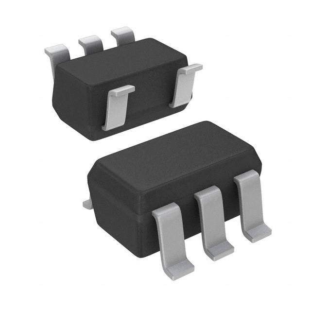
| 供应商器件封装 | SOT-23-5 |
| 共模抑制比—最小值 | 85 dB |
| 其它名称 | 296-14176-1 |
| 包装 | 剪切带 (CT) |
| 单位重量 | 17.500 mg |
| 压摆率 | 400 V/µs |
| 商标 | Texas Instruments |
| 增益带宽生成 | 200 MHz |
| 增益带宽积 | 200MHz |
| 安装类型 | 表面贴装 |
| 安装风格 | SMD/SMT |
| 封装 | Reel |
| 封装/外壳 | SC-74A,SOT-753 |
| 封装/箱体 | SOT-23-5 |
| 工作温度 | -40°C ~ 85°C |
| 工作电源电压 | 12 V |
| 工厂包装数量 | 250 |
| 拓扑结构 | Voltage Feedback |
| 放大器类型 | 电压反馈 |
| 最大工作温度 | + 85 C |
| 最小工作温度 | - 40 C |
| 标准包装 | 1 |
| 电压-电源,单/双 (±) | 10 V ~ 12 V, ±5 V ~ 6 V |
| 电压-输入失调 | 300µV |
| 电压增益dB | 110 dB |
| 电流-电源 | 20.2mA |
| 电流-输入偏置 | 20µA |
| 电流-输出/通道 | 100mA |
| 电源电流 | 20.8 mA |
| 电路数 | 1 |
| 稳定时间 | 15 ns |
| 系列 | OPA842 |
| 设计资源 | http://www.digikey.com/product-highlights/cn/zh/texas-instruments-webench-design-center/3176 |
| 转换速度 | 400 V/us |
| 输入补偿电压 | 1.2 mV |
| 输出电流 | 100 mA |
| 输出类型 | - |
| 通道数量 | 1 Channel |
| 配用 | /product-detail/zh/DEM-OPA-SOT-1A/296-20840-ND/1216445 |


- 商务部:美国ITC正式对集成电路等产品启动337调查
- 曝三星4nm工艺存在良率问题 高通将骁龙8 Gen1或转产台积电
- 太阳诱电将投资9.5亿元在常州建新厂生产MLCC 预计2023年完工
- 英特尔发布欧洲新工厂建设计划 深化IDM 2.0 战略
- 台积电先进制程称霸业界 有大客户加持明年业绩稳了
- 达到5530亿美元!SIA预计今年全球半导体销售额将创下新高
- 英特尔拟将自动驾驶子公司Mobileye上市 估值或超500亿美元
- 三星加码芯片和SET,合并消费电子和移动部门,撤换高东真等 CEO
- 三星电子宣布重大人事变动 还合并消费电子和移动部门
- 海关总署:前11个月进口集成电路产品价值2.52万亿元 增长14.8%


PDF Datasheet 数据手册内容提取
OPA842 www.ti.com SBOS267D–NOVEMBER2002–REVISEDSEPTEMBER2010 Wideband, Low Distortion, Unity-Gain Stable, Voltage-Feedback OPERATIONAL AMPLIFIER CheckforSamples:OPA842 FEATURES DESCRIPTION 1 • UNITY-GAINBANDWIDTH:400MHz The OPA842 provides a level of speed and dynamic 2 • GAIN-BANDWIDTHPRODUCT:200MHz range previously unattainable in a monolithic op amp. Using unity-gain stable, voltage-feedback architecture • LOWINPUTVOLTAGENOISE:2.6nV/√Hz with two internal gain stages, the OPA842 achieves • VERYLOWDISTORTION:–93dBc(5MHz) exceptionally low harmonic distortion over a wide • HIGHOPEN-LOOPGAIN:110dB frequency range. The classic differential input providesallthefamiliarbenefitsofprecisionopamps, • FAST12-BITSETTLING:22ns(0.01%) such as bias current cancellation and very low • LOWDCVOLTAGEOFFSET:300mVTypical inverting current noise compared with wideband • PROFESSIONALLEVELDIFFGAIN/PHASE current differential gain/phase performance, ERROR:0.003%/0.008° low-voltage noise, and high output current drive make the OPA842 ideal for most high dynamic range APPLICATIONS applications. • ADC/DACBUFFERDRIVER Unity-gain stability makes the OPA842 particularly • LOWDISTORTIONIFAMPLIFIER suitable for low-gain differential amplifiers, transimpedance amplifiers, gain of +2 video line • ACTIVEFILTERCONFIGURATION drivers, wideband integrators, and low-distortion • LOW-NOISEDIFFERENTIALRECEIVER analog-to-digital converter (ADC) buffers. Where • HIGH-RESOLUTIONIMAGING higher gain or even lower harmonic distortion is • TESTINSTRUMENTATION required, consider the OPA843—a higher-gain • PROFESSIONALAUDIO bandwidthandlower-noiseversionoftheOPA842. • OPA642UPGRADE OPA842RELATEDPRODUCTS INPUTNOISE GAIN-BANDWIDTH SINGLES VOLTAGE(nV/√Hz) PRODUCT(MHz) OPA843 2.0 800 OPA846 1.1 2500 OPA847 0.8 3700 +5V +5V REFT R 2kW 2kW S (+3V) VIN 0.1mF 24.9W OPA842 IN 50W 100pF ADS850 -5V 14-Bit 10MSPS 402W 2kW IN 402W 0.1mF (+2V) (+1V) 2kW REFB VREF SEL AC-Coupledto14-BitADS850Interface 1 Pleasebeawarethatanimportantnoticeconcerningavailability,standardwarranty,anduseincriticalapplicationsofTexas Instrumentssemiconductorproductsanddisclaimerstheretoappearsattheendofthisdatasheet. Alltrademarksarethepropertyoftheirrespectiveowners. 2 PRODUCTIONDATAinformationiscurrentasofpublicationdate. Copyright©2002–2010,TexasInstrumentsIncorporated Products conform to specifications per the terms of the Texas Instruments standard warranty. Production processing does not necessarilyincludetestingofallparameters.
OPA842 SBOS267D–NOVEMBER2002–REVISEDSEPTEMBER2010 www.ti.com This integrated circuit can be damaged by ESD. Texas Instruments recommends that all integrated circuits be handled with appropriateprecautions.Failuretoobserveproperhandlingandinstallationprocedurescancausedamage. ESDdamagecanrangefromsubtleperformancedegradationtocompletedevicefailure.Precisionintegratedcircuitsmaybemore susceptibletodamagebecauseverysmallparametricchangescouldcausethedevicenottomeetitspublishedspecifications. ORDERINGINFORMATION(1) SPECIFIED PACKAGE TEMPERATURE PACKAGE ORDERING TRANSPORT PRODUCT PACKAGE-LEAD DESIGNATOR RANGE MARKING NUMBER MEDIA,QUANTITY OPA842ID Rails,100 OPA842 SO-8 D -40°Cto+85°C OPA842 OPA842IDR TapeandReel,2500 OPA842IDBVT TapeandReel,250 OPA842 SOT23-5 DBV -40°Cto+85°C OAQI OPA842IDBVR TapeandReel,3000 (1) Forthemostcurrentpackageandorderinginformation,seethePackageOptionAddendumlocatedattheendofthisdatasheet,orsee deviceproductfolderatwww.ti.com. ABSOLUTE MAXIMUM RATINGS(1) Overoperatingfree-airtemperaturerange,unlessotherwisenoted. OPA842 UNIT PowerSupply ±6.5 VDC InternalPowerDissipation SeeThermalAnalysis DifferentialInputVoltage ±1.2 V InputVoltageRange ±VS V StorageTemperatureRange(Tstg):D,DBV –65to+125 °C JunctionTemperature(TJ) +175 °C HumanBodyModel(HBM) 2000 V ESDRatings ChargeDeviceModel(CDM) 1500 V MachineModel(MM) 200 V (1) Stressesabovetheseratingsmaycausepermanentdamage.Exposuretoabsolutemaximumconditionsforextendedperiodsmay degradedevicereliability.Thesearestressratingsonly,andfunctionaloperationofthedeviceattheseoranyotherconditionsbeyond thosespecifiedisnotsupported. DPACKAGE DRBPACKAGE SO-8 SOT23-5 (TOPVIEW) (TOPVIEW) NC 1 8 NC Output 1 5 +VS Inverting Input 2 7 +V S Noninverting Input 3 6 Output -VS 2 -VS 4 5 NC Noninverting Input 3 4 Inverting Input NC=Noconnection. 5 4 OAQI 1 2 3 Pin Orientation/Package Marking 2 Copyright©2002–2010,TexasInstrumentsIncorporated ProductFolderLink(s):OPA842
OPA842 www.ti.com SBOS267D–NOVEMBER2002–REVISEDSEPTEMBER2010 ELECTRICAL CHARACTERISTICS: V = ±5V S Boldfacelimitsaretestedat+25°C.AtT =+25°C,V =±5V,R =402Ω,R =100Ω,andG=+2,unlessotherwisenoted. A S F L SeeFigure37foracperformance. OPA842ID,IDBV MIN/MAXOVER TYP TEMPERATURE 0°Cto -40°Cto MIN/ TEST PARAMETER TESTCONDITIONS +25°C +25°C(2) +70°C(3) +85°C(3) UNIT MAX LEVELS(1) ACPerformance(seeFigure37) C10lo0smeVd-PLPo)opBandwidth(VO= G=+1,RF=25Ω 350 MHz typ C G=+2 150 105 101 100 MHz min B G=+5 45 30 29 29 MHz min B G=+10 21 15 14 14 MHz min B Gain-BandwidthProduct 200 136 135 135 MHz min B Bandwidthfor0.1dBGainFlatness G=+2,RL=100Ω,VO=100mVPP 56 MHz typ C G=+1,RL=100Ω,RF=25Ω 105 MHz typ C HarmonicDistortion G=+2,f=5MHz,VO=2VPP xxxsecond-Harmonic RL=100Ω –80 –78 –77 –76 dBc max B RL=500Ω –94 –92 –91 –90 dBc max B xxxthird-Harmonic RL=100Ω –97 –96 –95 –94 dBc max B RL=500Ω –93 –91 –90 –90 dBc max B Two-Tone,Third-OrderIntercept G=+2,f=10MHz 44 dBm typ C InputVoltageNoise f>1MHz 2.6 2.8 3.0 3.1 nV/√Hz max B InputCurrentNoise f>1MHz 2.7 2.8 2.9 3.0 pA/√Hz max B RiseandFallTime 0.2VStep 2.3 3.3 3.4 3.5 ns max B SlewRate 2VStep 400 300 250 225 V/ms min B SettlingTimeto0.01% 2VStep 22 ns typ C SettlingTimeto0.1% 2VStep 15 19.6 20.3 21.3 ns max B SettlingTimeto1.0% 2VStep 9 10.2 11.3 12.5 ns max B DifferentialGain G=+2,NTSC,RL=150Ω 0.003 % typ C DifferentialPhase G=+2,NTSC,RL=150Ω 0.008 degrees typ C DCPERFORMANCE(4) Open-LoopVoltageGain(AOL) VO=0V 110 100 96 92 dB min A InputOffsetVoltage VCM=0V ±0.30 ±1.2 ±1.4 ±1.5 mV max A AverageOffsetVoltageDrift VCM=0V ±4 ±4 mV/°C max B InputBiasCurrent VCM=0V –20 –35 –36 –37 mA max A InputBiasCurrentDrift VCM=0V 25 25 nA/°C max B InputOffsetCurrent VCM=0V ±0.35 ±1.0 ±1.15 ±1.17 mA max A InputOffsetCurrentDrift VCM=0V ±2 ±2 nA/°C max B INPUT Common-ModeInputRange(5) ±3.2 ±3.0 ±2.9 ±2.8 V min A (CMIR) Common-ModeRejectionRatio (CMRR) VCM=±1V,Input-Referred 95 85 84 82 dB min A InputImpedance xxxDifferentialMode VCM=0V 14||1 kΩ||pF typ C xxxCommon-Mode VCM=0V 3.1||1.2 MΩ||pF typ C (1) Testlevels:(A)100%testedat+25°C.Overtemperaturelimitsbycharacterizationandsimulation.(B)Limitssetbycharacterizationand simulation.(C)Typicalvalueonlyforinformation. (2) Junctiontemperature=ambienttemperaturefor+25°Cspecifications. (3) Junctiontemperature=ambientatlowtemperaturelimits;junctiontemperature=ambient+23°Cathightemperaturelimitforover- temperaturemin/maxspecifications. (4) Currentisconsideredpositiveout-of-node.V istheinputcommon-modevoltage. CM (5) Tested<3dBbelowminimumspecifiedCMRRat±CMIRlimits. Copyright©2002–2010,TexasInstrumentsIncorporated 3 ProductFolderLink(s):OPA842
OPA842 SBOS267D–NOVEMBER2002–REVISEDSEPTEMBER2010 www.ti.com ELECTRICAL CHARACTERISTICS: V = ±5V (continued) S Boldfacelimitsaretestedat+25°C.AtT =+25°C,V =±5V,R =402Ω,R =100Ω,andG=+2,unlessotherwisenoted. A S F L SeeFigure37foracperformance. OPA842ID,IDBV MIN/MAXOVER TYP TEMPERATURE 0°Cto -40°Cto MIN/ TEST PARAMETER TESTCONDITIONS +25°C +25°C(2) +70°C(3) +85°C(3) UNIT MAX LEVELS(1) OUTPUT OutputVoltageSwing RL>1kΩ,PositiveOutput 3.2 3.0 ±2.9 ±2.8 V min A RL>1kΩ,NegativeOutput –3.7 –3.5 –3.4 –3.3 V min A RL=100Ω,PositiveOutput 3.0 2.8 2.7 2.6 V min A RL=100Ω,NegativeOutput –3.5 –3.3 –3.2 –3.1 V min A CurrentOutput,Sourcing VO=0V ±100 ±90 ±85 ±80 mA min A Closed-LoopOutputImpedance G=+2,f=1kHz 0.00038 Ω typ C POWERSUPPLY SpecifiedOperatingVoltage ±5 V typ C MaximumOperatingVoltage ±6 ±6 ±6 V min A MinimumOperatingVoltage ±3.5 V typ C MaximumQuiescentCurrent VS=±5V 20.2 20.8 22.2 22.5 mA max A MinimumQuiescentCurrent VS=±5V 20.2 19.6 19.1 18.3 mA min A Power-SupplyRejectionRatio min (+PSRR,–PSRR) |VS|=4.5Vto5.5V,Input-Referred 100 90 88 85 dB A THERMALCHARACTERISTICS SpecifiedOperatingRange:D,DBV –40to+85 °C typ C ThermalResistance,qJA Junction-to-Ambient — — — — xxxDxxxxxSO-8 125 °C/W typ C xxxDBVxxxSOT23 150 °C/W typ C 4 Copyright©2002–2010,TexasInstrumentsIncorporated ProductFolderLink(s):OPA842
OPA842 www.ti.com SBOS267D–NOVEMBER2002–REVISEDSEPTEMBER2010 TYPICAL CHARACTERISTICS: V = ±5V S AtT =+25°C,G=+2,R =402Ω,andR =100Ω,unlessotherwisenoted. A F L NONINVERTINGSMALL−SIGNAL INVERTINGSMALL−SIGNAL FREQUENCYRESPONSE FREQUENCYRESPONSE 3 3 G = +1 R =25W 0 F 0 div) G = +2 div) G =-1 B/ -3 B/ -3 3d VO= 0.1VPP G = +5 3d VO= 0.1VPP G =-2 n ( -6 n ( -6 ai ai G G = +10 G G =-5 d -9 d -9 e e z z ali ali m -12 m -12 or or G =-10 N N -15 -15 See Figure 37 See Figure 38 -18 -18 1 10 100 500 1 10 100 500 Frequency (MHz) Frequency (MHz) Figure1. Figure2. NONINVERTINGLARGE−SIGNAL INVERTINGLARGE−SIGNAL FREQUENCYRESPONSE FREQUENCYRESPONSE 9 9 0.1VPP 0.1VPP div) 6 01..50VVPPPP 63 RGL ==- 120V0/WV 12VVPPPP B/ 3 zed Gain (3d -03 RGL == + 120V0/WV VVOO== 2 5VVPPPP ain (3dB/div) --036 RG= 200W 5VPP ali G -9 m -6 or -12 N -9 -15 See Figure 37 See Figure 38 -12 -18 1 10 100 500 1 10 100 500 Frequency (MHz) Frequency (MHz) Figure3. Figure4. NONINVERTINGPULSERESPONSE INVERTINGPULSERESPONSE Large Signal 1V G =-2 Large Signal 1V 1.2 R = 200W 1.2 v) G = +2 O v) G O 0mV/di 210000 Right Scale 00..84 utput V 0mV/di 210000 Right Scale 00..84 utput V 0 o 0 o ge (1 0 0 ltage ge (1 0 0 ltage Volta -100 SmallL Seifgt nSacla l1e00mV -0.4 (400 Volta -100 SmallL Seifgt nSacla l1e00mV -0.4 (400 Output -200 -0.8 mV/div Output -200 -0.8 mV/div ) ) -1.2 -1.2 See Figure 37 See Figure 38 Time (5ns/div) Time (5ns/div) Figure5. Figure6. Copyright©2002–2010,TexasInstrumentsIncorporated 5 ProductFolderLink(s):OPA842
OPA842 SBOS267D–NOVEMBER2002–REVISEDSEPTEMBER2010 www.ti.com TYPICAL CHARACTERISTICS: V = ±5V (continued) S AtT =+25°C,G=+2,R =402Ω,andR =100Ω,unlessotherwisenoted. A F L 5MHzHARMONICDISTORTION 1MHzHARMONICDISTORTION vsLOADRESISTANCE vsLOADRESISTANCE -75 -85 V = 2V V = 2V O PP O PP c) -80 c) -90 B B d d n ( 2nd Harmonic n ( stortio -85 stortio -95 2nd Harmonic Di Di c -90 c -100 ni ni o o m m ar ar H -95 H -105 3rd Harmonic 3rd Harmonic See Figure 37 See Figure 37 -100 -110 100 150 200 250 300 350 400 450 500 100 150 200 250 300 350 400 450 500 Load Resistance (W) Load Resistance (W) Figure7. Figure8. HARMONICDISTORTION HARMONICDISTORTION vsFREQUENCY vsOUTPUTVOLTAGE -60 -80 VO= 2VPP RL= 200W RL= 200W -85 f = 5MHZ Bc) -70 G = +2 Bc) d d n ( n ( -90 onic Distortio --8900 2nd Harmonic onic Distortio -1-0905 2nd Harmonic 3rd Harmonic m 3rd Harmonic m ar ar H -100 H -105 See Figure 37 See Figure 37 -110 -110 0.5 1 10 20 0.1 1 10 Frequency (MHz) Output Voltage Swing (V ) PP Figure9. Figure10. HARMONICDISTORTION HARMONICDISTORTION vsNONINVERTINGGAIN vsINVERTINGGAIN -70 -70 VO= 2VPP VO= 2VPP RL= 200W RL= 200W Bc) -80 f = 5MHz Bc) -80 f = 5MHz n (d 2nd Harmonic n (d RF= 402W 2nd Harmonic o o orti orti Dist -90 Dist -90 nic 3rd Harmonic nic o o m m ar -100 ar -100 H H 3rd Harmonic See Figure 37 See Figure 38 -110 -110 1 10 1 10 Noninverting Gain (V/V) Inverting Gain |V/V| Figure11. Figure12. 6 Copyright©2002–2010,TexasInstrumentsIncorporated ProductFolderLink(s):OPA842
OPA842 www.ti.com SBOS267D–NOVEMBER2002–REVISEDSEPTEMBER2010 TYPICAL CHARACTERISTICS: V = ±5V (continued) S AtT =+25°C,G=+2,R =402Ω,andR =100Ω,unlessotherwisenoted. A F L TWO−TONE,THIRD−ORDER INPUTVOLTAGEANDCURRENTNOISE INTERMODULATIONINTERCEPT 100 50 PI 50W 45 50W OPA842 PO e (nV/Ö)Hze (pA/)HzÖ nt (+dBm) 40 402W402W 50W oisois 10 Poi 35 Voltage NCurrent N Voltage Noise Cu2r.7repnAt /NÖHoizse Intercept 30 25 2.6nV/ÖHz 1 20 102 103 104 105 106 107 5 10 15 20 25 30 35 40 45 50 Frequency (Hz) Frequency (MHz) Figure13. Figure14. RECOMMENDEDR vsCAPACITIVELOAD FREQUENCYRESPONSEvsCAPACITIVELOAD S 100 B) 3 d d ( 0 oa C = 10pF L ve -3 citi C = 47pF C = 22pF a )W ap -6 ( 10 C C = 100pF RS n to -9 ai VI RS zed G -12 50W OP4A0824W2 CL 1kWVO ali -15 m 402W or 1 N -18 1 10 100 1k 10 100 500 Capacitive Load (pF) Frequency (MHz) Figure15. Figure16. GAIN=+1FLATNESS PULSERESPONSEG=+1 0.2 Large Signal 1V 0.1 1.2 v) O -0.01 VO= 0.1VPP 00mV/di 210000 Right Scale 00..84 utput Vo Gain (dB) --00..23 RRFL== 12050WW Voltage (1 -1000 SLmeaftl l SSciganleal 0-0.4 ltage (400 -0.4 Output -200 -0.8 mV/div ) -1.2 -0.5 -0.6 Time (2ns/div) 0 25 50 75 100 125 150 175 200 Frequency (MHz) Figure17. Figure18. Copyright©2002–2010,TexasInstrumentsIncorporated 7 ProductFolderLink(s):OPA842
OPA842 SBOS267D–NOVEMBER2002–REVISEDSEPTEMBER2010 www.ti.com TYPICAL CHARACTERISTICS: V = ±5V (continued) S AtT =+25°C,G=+2,R =402Ω,andR =100Ω,unlessotherwisenoted. A F L COMMON−MODEREJECTIONRATIOAND POWER−SUPPLYREJECTIONRATIOvsFREQUENCY OPEN−LOOPGAINANDPHASE 120 120 0 -PSRR 20log (A ) OL 100 -30 100 CMRR dB) 80 -60 Op R (dB)R (dB) 8600 +PSRR p Gain ( 60 ÐAOL -90 en-Loop CMRPSR 40 en-Loo 40 -120 Phase Op 20 -150 ()° 20 0 -180 0 -20 -210 101 102 103 104 105 106 107 108 101 102 103 104 105 106 107 108 109 Frequency (Hz) Frequency (Hz) Figure19. Figure20. CLOSED-LOOPOUTPUTIMPEDANCE OUTPUTVOLTAGEANDCURRENTLIMITATIONS vsFREQUENCY 4 10 3 1 2 )W RL= 100 e ( 0.1 1 c V(V)O -01 P1Wow Ienrt eLrinmaitl RL= R50L= 25 put Impedan 0.00.0011 ut -2 1W Internal O Power Limit 0.0001 -3 -4 0.00001 -0.15 -0.10 -0.05 0 0.05 0.10 0.15 102 103 104 105 106 107 108 IO(mA) Frequency (Hz) Figure21. Figure22. NONINVERTINGOVERDRIVERECOVERY INVERTINGOVERDRIVERECOVERY 8 4 8 4 Input RL= 100W Input RL= 100W 6 Right Scale G = 2 3 6 Right Scale G = 2 3 See Figure 37 See Figure 38 V/div) 4 Output 2 Inpu V/div) 4 2 Inpu ut Voltage (2 -202 Left Scale 10-1 t Voltage (1V ut Voltage (2 -202 10-1 t Voltage (1V Outp -4 -2 /div) Outp -4 Output -2 /div) -6 -3 -6 Left Scale -3 -8 -4 -8 -4 Time (40ns/div) Time (40ns/div) Figure23. Figure24. 8 Copyright©2002–2010,TexasInstrumentsIncorporated ProductFolderLink(s):OPA842
OPA842 www.ti.com SBOS267D–NOVEMBER2002–REVISEDSEPTEMBER2010 TYPICAL CHARACTERISTICS: V = ±5V (continued) S AtT =+25°C,G=+2,R =402Ω,andR =100Ω,unlessotherwisenoted. A F L SETTLINGTIME VIDEODIFFERENTIALGAIN/DIFFERENTIALPHASE 0.250 0.008 0.08 V = 2V Step G = 2 0.200 O R = 100W L Percent of Final Value (%) ---000000......1100115055050000000 G = 2 Differential Gain (%) 000...000000642 DG Negative Video DDP GN ePgVoasidDtiiteviPveo eP Vosiditeivoe Video 000...000642 Differential Phase ()° -0.200 See Figure 37 -0.250 0 0 0 5 10 15 20 25 30 35 40 45 50 1 2 3 4 5 Video Loads Time (ns) Figure25. Figure26. TYPICALDCDRIFTOVERTEMPERATURE SUPPLYANDOUTPUTCURRENTvsTEMPERATURE 1 25 120 24 100x (Input Offset Current) Right Scale In 115 22 Input Offset Voltage (mV) -00..505 InputL Oefftf sSect aVloeIlntapguet Bias Current 10-122.5.5 put Bias and Offset Current (A Output Current (5mA/div) 1111009905050 SSuipnRpk/liySg ohCutLu rSercrcfeeta nSOletcuatpleut Current 2111108642 Supply Current (2mA/div) ) 85 10 Right Scale -1 -25 -50 -25 0 25 50 75 100 125 80 8 -50 -25 0 25 50 75 100 125 Ambient Temperature (°C) Ambient Temperature (°C) Figure27. Figure28. COMMON-MODEINPUTRANGEANDOUTPUTSWING vsSUPPLYVOLTAGE COMMON-MODEANDDIFFERENTIALINPUTIMPEDANCE 6 7 10 Common-Mode Impedance 4 6 10 nge (V) 2 nce ()W 105 Ra 0 da e ±Voltage Output ±Voltage Input pe Voltag -2 put Im 104 Differential Impedance n I 3 -4 10 -6 2 10 3 4 5 6 102 103 104 105 106 107 108 109 Supply Voltage (V) Frequency (Hz) Figure29. Figure30. Copyright©2002–2010,TexasInstrumentsIncorporated 9 ProductFolderLink(s):OPA842
OPA842 SBOS267D–NOVEMBER2002–REVISEDSEPTEMBER2010 www.ti.com TYPICAL CHARACTERISTICS: V = ±5V (continued) S AtT =+25°C,G=+2,R =402Ω,andR =100Ω,unlessotherwisenoted. A F L DIFFERENTIALSMALL-SIGNAL DIFFERENTIALPERFORMANCETESTCIRCUIT FREQUENCYRESPONSE +5V 3 G = 1 D 0 OP-A58V42 GD= 40R2GW Gain (dB) --36 GD= 5 GD= 2 d G = 10 RG 402W alize -9 D m or -12 VI RG 402W RL VO N -15 +5V -18 1 10 100 500 OPA842 Frequency (MHz) -5V Figure31. Figure32. DIFFERENTIALLARGE-SIGNALFREQUENCYRESPONSE DIFFERENTIALDISTORTIONvsLOADRESISTANCE 9 -85 G = 2 6 f = 5MHz 3 GRLD== 4200W 012.VV2PVPPP n (dBc) -90 VO= 4VPP Gain (dB) -03 PP 5VPP nic Distortio -1-0905 2nd Harmonic o -6 m ar 8V H -105 -9 PP 3rd Harmonic -12 -110 10 100 500 50 100 150 200 250 300 350 400 450 500 Frequency (MHz) Load Resistance (W) Figure33. Figure34. DIFFERENTIALDISTORTIONvsFREQUENCY DIFFERENTIALDISTORTIONvsOUTPUTVOLTAGE -60 -80 RL= 400W RL= 400W VO= 4VPP -85 GD= +2 Bc) -70 GD= +2 Bc) f = 5MHz d d -90 n ( n ( nic Distortio --8900 nic Distortio -1-0905 2nd Harmonic mo 2nd Harmonic mo -105 Har -100 Har 3rd Harmonic -110 3rd Harmonic -110 -115 1 10 100 1 10 Frequency (MHz) Output Voltage Swing (V ) PP Figure35. Figure36. 10 Copyright©2002–2010,TexasInstrumentsIncorporated ProductFolderLink(s):OPA842
OPA842 www.ti.com SBOS267D–NOVEMBER2002–REVISEDSEPTEMBER2010 APPLICATION INFORMATION WIDEBAND CURRENT FEEDBACK OPERATION WIDEBAND INVERTING OPERATION The OPA842 combination of speed and dynamic Operating the OPA842 as an inverting amplifier has range is easily achieved in a wide variety of several benefits and is particularly useful when a application circuits, providing that simple principles of matched 50Ω source and input impedance is good design practice are observed. For example, required. Figure 38 shows the inverting gain of –2 good power-supply decoupling, as shown in circuitusedasthebasisoftheinvertingmodeTypical Figure 37, is essential to achieve the lowest possible Characteristics. harmonicdistortionandsmoothfrequencyresponse. +5V Proper printed circuit board (PCB) layout and careful component selection will maximize the performance of the OPA842 in all applications, as discussed in the followingsectionsofthisdatasheet. + 0.1mF 2.2mF Figure 37 shows the gain of +2 configuration used as 50WLoad the basis for most of the Typical Characteristics. Most V 50W ofthecurveswerecharacterizedusingsignalsources 0.1mF RT OPA842 O 147W with 50Ω driving impedance and with measurement equipment presenting 50Ω load impedance. In Figure 37, the 50Ω shunt resistor at the V terminal R R I 50WSource G F matches the source impedance of the test generator 200W 402W V while the 50Ω series resistor at the V terminal I O provides a matching resistor for the measurement R M equipment load. Generally, data sheet specifications 66.5W 0.1mF 2.2mF refer to the voltage swing at the output pin (V in + O Figure 37). The 100Ω load, combined with the 804Ω -5V total feedback network load, presents the OPA842 with an effective load of approximately 90Ω in Figure38. InvertingG=–2Specificationsand Figure37. TestCircuit +5V In the inverting case, just the feedback resistor +V S appearsaspartofthetotaloutputloadinparallelwith theactualload.Forthe100Ω loadusedintheTypical Characteristics, this gives a total load of 80Ω in this + 0.1mF 2.2mF inverting configuration. The gain resistor is set to get 50WSource the desired gain (in this case, 200Ω for a gain of –2) R 50WLoad S while an additional input matching resistor (R ) can VIN 50W OPA842 VO 50W be used to set the total input impedance equalMto the source if desired. In this case, R = 66.5Ω in parallel M with the 200Ω gain setting resistor gives a matched RF input impedance of 50Ω. This matching is only 402W needed when the input needs to be matched to a source impedance, as in the characterization testing R done using the circuit of Figure 38. The OPA842 G 402W offers extremely good dc accuracy as well as low 0.1mF 2.2mF + noise and distortion. To take full advantage of that dc precision, the total dc impedance looking out of each -V of the input nodes must be matched to get bias S -5V current cancellation. For the circuit of Figure 38, this requires the 147Ω resistor shown to ground on the Figure37. Gainof+2,High-Frequency noninverting input. The calculation for this resistor ApplicationandCharacterizationCircuit includes a dc-coupled 50Ω source impedance along Copyright©2002–2010,TexasInstrumentsIncorporated 11 ProductFolderLink(s):OPA842
OPA842 SBOS267D–NOVEMBER2002–REVISEDSEPTEMBER2010 www.ti.com with R and R . Although this resistor will provide SFDR is often obtained by adding this external G M cancellation for the bias current, it must be capacitor, whose value is often recommended in this well-decoupled (0.1mF in Figure 38) to filter the noise converter data sheet. The external capacitor, in contribution of the resistor and the input current combination with the built-in capacitance of the ADC noise. input, presents a significant capacitive load to the OPA842. Without a series isolation resistor, an As the required R resistor approaches 50Ω at higher G undesirable peaking or loss of stability in the amplifier gains, the bandwidth for the circuit in Figure 38 will mayresult. far exceed the bandwidth at that same gain magnitude for the noninverting circuit of Figure 37. Since the dc bias current of the CMOS ADC input is This occurs due to the lower noise gain for the circuit negligible, the resistor has no effect on overall gain or of Figure 38 when the 50Ω source impedance is offset accuracy. Refer to the Typical Characteristic included in the analysis. For instance, at a signal gain graph, R vs Capacitive Load (Figure 15) to obtain a S of –8 (R = 50Ω, R = open, R = 402Ω) the noise good starting value for the series resistor. This will G M F gain for the circuit of Figure 38 will be 1 + 402Ω/(50Ω ensure flat frequency response to the ADC input. + 50Ω) = 5 due to the addition of the 50Ω source in Increasing the external capacitor value will allow the the noise gain equation. This gives considerable series resistor to be reduced. Intentionally higher bandwidth than the noninverting gain of +8. bandlimiting using this RC network can also be used Using the 200MHz gain bandwidth product for the tolimitnoiseattheconverterinput. OPA842, an inverting gain of –8 from a 50Ω source to a 50Ω R will give approximately 40MHz VIDEO LINE DRIVING G bandwidth, whereas the noninverting gain of +8 will Most video distribution systems are designed with give25MHz. 75Ω series resistors to drive a matched 75Ω cable. In order to deliver a net gain of 1 to the 75Ω matched BUFFERING HIGH-PERFORMANCE ADCs load, the amplifier is typically set up for a voltage gain To achieve full performance from a high dynamic of +2, compensating for the 6dB attenuation of the range ADC, considerable care must be exercised in voltage divider formed by the series and shunt 75Ω the design of the input amplifier interface circuit. The resistorsateitherendofthecable. example circuit on the front page shows a typical The circuit of Figure 37 applies to this requirement if ac-coupled interface to a very high dynamic range all references to 50Ω resistors are replaced by 75Ω converter. This ac-coupled example allows the values. Often, the amplifier gain is further increased OPA842 to be operated using a signal range that to 2.2, which recovers the additional dc loss of a swings symmetrically around ground (0V). The 2V PP typical long cable run. This change would require the swing is then level-shifted through the blocking gain resistor (R ) in Figure 37 to be reduced from capacitor to a midscale reference level, which is G 402Ω to 335Ω. In either case, both the gain flatness created by a well-decoupled resistive divider off the and the differential gain/phase performance of the converter internal reference voltages. To have a OPA842 will provide exceptional results in video negligible effect on the rated spurious-free dynamic distribution applications. Differential gain and phase range (SFDR) of the converter, the amplifier SFDR measure the change in overall small-signal gain and should be at least 10dB greater than the converter. phase for the color sub-carrier frequency (3.58MHz in The OPA842 has no effect on the rated distortion of NTSC systems) versus changes in the large-signal the ADS850, given its 82dB SFDR at 2V , 5MHz. PP output level (which represents luminance information The greater than 92dB SFDR for the OPA842 in this in a composite video signal). The OPA842, with the configurationwillnotdegradetheconverter. typical 150Ω load of a single matched video cable, SuccessfulapplicationoftheOPA842forADCdriving shows less than 0.01%/0.01° differential gain/phase requires careful selection of the series resistor at the errors over the standard luminance range for a amplifier output, along with the additional shunt positive video (negative sync) signal. Similar capacitor at the ADC input. To some extent, selection performance would be observed for negative video of this RC network will be determined empirically for signals. each model of the converter. Many high-performance CMOS ADCs, like the ADS850, perform better with the shunt capacitor at the input pin. This capacitor provides low source impedance for the transient currentsproducedbythesamplingprocess.Improved 12 Copyright©2002–2010,TexasInstrumentsIncorporated ProductFolderLink(s):OPA842
OPA842 www.ti.com SBOS267D–NOVEMBER2002–REVISEDSEPTEMBER2010 SINGLE OP AMP DIFFERENTIAL AMPLIFIER THREE OP AMP DIFFERENCING (Instrumentation Topology) The voltage-feedback architecture of the OPA842, with its high Common-Mode Rejection Ratio (CMRR), The primary drawback of the single op amp will provide exceptional performance in differential differential amplifier is its relatively low input amplifier configurations. Figure 39 shows a typical impedance. Where high impedance is required at the configuration. The starting point for this design is the differential input, a standard instrumentation amplifier selectionoftheR valueintherangeof200Ω to2kΩ. (INA) topology may be built using the OPA842 as the F Lower values reduce the required R , increasing the differencing stage. Figure 40 shows an example of G load on the V source and on the OPA842 output. this, in which the two input amplifiers are packaged 2 Higher values increase output noise and exacerbate together as a dual voltage-feedback op amp, the the effects of parasitic board and device OPA2822. This approach saves board space, cost, capacitances. Following the selection of R , R must and power compared to using two additional OPA842 F G be set to achieve the desired inverting gain for V . devices, and still achieves very good noise and 2 Remember that the bandwidth will be set distortion performance due to the moderate loading approximately by the Gain Bandwidth Product (GBP) ontheinputamplifiers. divided by the noise gain (1 + R /R ). For accurate F G differential operation (that is, good CMRR), the ratio +5V R /R mustbesetequaltoR /R . 2 1 F G V 1 +5V OPA2822 Power-supply decoupling not shown. R1 Power-supply decoupling not shown. RF1 +5V V 500W 500W 1 50W R R2 OPA842 VO=RFG(V1-V2) RG R 500W OPA842 VO 500W F1 500W R R -5V V RG RF whenR21=RFG 500W 500W 2 OPA2822 -5V V 2 Figure39. High-Speed,SingleDifferential -5V Amplifier Figure40. WidebandThree-OpAmpDifferencing Usually, it is best to set the absolute values of R and Amplifier 2 R equal to R and R , respectively; this equalizes 1 F G the divider resistances and cancels the effect of input In this circuit, the common-mode gain to the output is bias currents. However, it is sometimes useful to always 1, due to the four matched 500Ω resistors, scale the values of R2 and R1 in order to adjust the whereas the differential gain is set by (1 + 2RF1/RG), loading on the driving source V1. In most cases, the which is equal to 2 using the values in Figure 40. The achievablelow-frequencyCMRRwillbelimitedbythe differential to single-ended conversion is still accuracy of the resistor values. The 85dB CMRR of performed by the OPA842 output stage. The the OPA842 itself will not determine the overall circuit high-impedanceinputsallowtheV andV sourcesto 1 2 CMRR unless the resistor ratios are matched to be terminated or impedance matched as required. If better than 0.003%. If it is necessary to trim the the V and V inputs are already truly differential, 1 2 CMRR,thenR2isthesuggestedadjustmentpoint. such as the output from a signal transformer, then a single matching termination resistor may be used between them. Remember, however, that a defined dc signal path must always exist for the V and V 1 2 inputs; for the transformer case, a center-tapped secondary connected to ground would provide an optimumdcoperatingpoint. Copyright©2002–2010,TexasInstrumentsIncorporated 13 ProductFolderLink(s):OPA842
OPA842 SBOS267D–NOVEMBER2002–REVISEDSEPTEMBER2010 www.ti.com DAC TRANSIMPEDANCE AMPLIFIER which will give a corner frequency (f ) of –3dB approximately: High-frequency digital-to-analog converters (DACs) require a low-distortion output amplifier to retain the GBP f = SFDR performance into real-world loads. A -3dB 2pR C single-ended output drive implementation is shown in F D (2) Figure 41. In this circuit, only one side of the complementary output drive signal is used. The ACTIVE FILTERS diagram shows the signal output current connected Most active filter topologies will have exceptional into the virtual ground-summing junction of the performance using the broad bandwidth and OPA842, which is set up as a transimpedance stage unity-gain stability of the OPA842. Topologies or I-V converter. The unused current output of the employing capacitive feedback require a unity-gain DAC is connected to ground. If the DAC requires its stable, voltage-feedback op amp. Sallen-Key filters outputsterminatedtoacompliancevoltageotherthan simply use the op amp as a noninverting gain stage ground for operation, then the appropriate voltage inside an RC network. Either current- or level may be applied to the noninverting input of the voltage-feedback op amps may be used in OPA842. Sallen-Keyimplementations. See Figure 42 for an example Sallen-Key low-pass filter, in which the OPA842 is set up to deliver a OPA842 V = I R low-frequency gain of +2. The filter component values O D F have been selected to achieve a maximally flat High-Speed Butterworth response with a 5MHz, –3dB bandwidth. DAC RF The resistor values have been slightly adjusted to compensate for the effects of the 150MHz bandwidth C provided by the OPA842 in this configuration. This F ID CD filter may be combined with the ADC driver suggestions to provide moderate (two-pole) Nyquist GBP?Gain Bandwidth filtering, limiting noise, and out-of-band harmonics Product (Hz) for the OPA842 into the input of an ADC. This filter will deliver the exceptionally low harmonic distortion required by high SFDR ADCs such as the ADS850 (14-bit, 10MSPS, I 82dBSFDR). D C 1 150pF Figure41. Wideband,Low-DistortionDAC +5V TransimpedanceAmplifier R R 1 2 124W 505W V The dc gain for this circuit is equal to R . At high 1 F C frequencies, the DAC output capacitance will produce 2 OPA842 V 100pF O a zero in the noise gain for the OPA842 that may RF cause peaking in the closed-loop frequency 402W response. CF is added across RF to compensate for Power-supply this noise-gain peaking. To achieve a flat decoupling not shown. transimpedance frequency response, this pole in the -5V R feedbacknetworkshouldbesetto: 40G2W 1 GBP = 2pR C 4pR C F F F D (1) Figure42. 5MHzButterworthLow-PassActive Filter 14 Copyright©2002–2010,TexasInstrumentsIncorporated ProductFolderLink(s):OPA842
OPA842 www.ti.com SBOS267D–NOVEMBER2002–REVISEDSEPTEMBER2010 DESIGN-IN TOOLS MACROMODELSANDAPPLICATIONSSUPPORT Computer simulation of circuit performance using DEMONSTRATIONFIXTURES SPICE is often a quick way to analyze the Two printed circuit boards (PCBs) are available to performance of the OPA842 and its circuit designs. assist in the initial evaluation of circuit performance This is particularly true for video and RF amplifier using the OPA842 in its two package options. Both of circuits where parasitic capacitance and inductance these are offered free of charge as unpopulated can play a major role on circuit performance. A PCBs, delivered with a user's guide. The summary SPICE model for the OPA842 is available through the informationforthesefixturesisshowninTable1. TI web page (www.ti.com). The applications group is also available for design assistance. These models Table1.DemonstrationFixturesbyPackage predict typical small-signal ac, transient steps, dc performance, and noise under a wide variety of ORDERING LITERATURE operating conditions. The models include the noise PRODUCT PACKAGE NUMBER NUMBER terms found in the Electrical Characteristics of the OPA842ID SO-8 DEM-OPA-SO-1A SBOU009 data sheet. These models do not attempt to OPA842IDBV SOT23-5 DEM-OPA-SOT-1A SBOU010 distinguish between the package types in the small-signalacperformance. The demonstration fixtures can be requested at the Texas Instruments web site (www.ti.com) through the OPA842productfolder. OPERATING SUGGESTIONS In the inverting configuration, an additional design OPTIMIZING RESISTOR VALUES consideration must be noted. R becomes the input G Since the OPA842 is a unity-gain stable, resistor and therefore the load impedance to the voltage-feedback op amp, a wide range of resistor driving source. If impedance matching is desired, R G values may be used for the feedback and gain setting may be set equal to the required termination value. resistors. The primary limits on these values are set However, at low inverting gains, the resultant by dynamic range (noise and distortion) and parasitic feedback resistor value can present a significant load capacitance considerations. For a noninverting to the amplifier output. For example, an inverting gain unity-gain follower application, the feedback of 2 with a 50Ω input matching resistor (equal to R ) G connection should be made with a 25Ω resistor—not would require a 100Ω feedback resistor, which would a direct short. This will isolate the inverting input contribute to output loading in parallel with the capacitance from the output pin and improve the external load. In such a case, it would be preferable frequency response flatness. Usually, the feedback to increase both the R and R values, and then F G resistor value should be between 200Ω and 1kΩ. achieve the input matching impedance with a third Below 200Ω, the feedback network will present resistor to ground (see Figure 38). The total input additional output loading which can degrade the impedance becomes the parallel combination of R G harmonic distortion performance of the OPA842. andtheadditionalshuntresistor. Above 1kΩ, the typical parasitic capacitance (approximately 0.2pF) across the feedback resistor BANDWIDTH vs GAIN may cause unintentional band limiting in the amplifier Voltage-feedback op amps exhibit decreasing response. closed-loop bandwidth as the signal gain is A good rule of thumb is to target the parallel increased. In theory, this relationship is described by combination of R and R (see Figure 37) to be less the GBP shown in the specifications. Ideally, dividing F G than about 200Ω. The combined impedance R || R GBP by the noninverting signal gain (also called the F G interacts with the inverting input capacitance, placing Noise Gain, or NG) will predict the closed-loop an additional pole in the feedback network, and thus bandwidth. In practice, this only holds true when the a zero in the forward response. Assuming a 2pF total phase margin approaches 90 degrees, as it does in parasitic on the inverting node, holding R || R < high-gain configurations. At low signal gains, most F G 200Ω will keep this pole above 400MHz. By itself, this amplifiers will exhibit a more complex response with constraint implies that the feedback resistor R can lower phase margin. The OPA842 is optimized to F increase to several kΩ at high gains. This is give a maximally flat second-order Butterworth acceptable as long as the pole formed by R and any response in a gain of 2. In this configuration, the F parasitic capacitance appearing in parallel is kept out OPA842 has approximately 60 degrees of phase ofthefrequencyrangeofinterest. margin and will show a typical –3dB bandwidth of 150MHz. When the phase margin is 60 degrees, the closed-loop bandwidth is approximately √2 greater Copyright©2002–2010,TexasInstrumentsIncorporated 15 ProductFolderLink(s):OPA842
OPA842 SBOS267D–NOVEMBER2002–REVISEDSEPTEMBER2010 www.ti.com thanthevaluepredictedbydividingGBPbythenoise The Typical Characteristics show the recommended gain. Increasing the gain will cause the phase margin R vs Capacitive Load (see Figure 15) and the S to approach 90 degrees and the bandwidth to more resulting frequency response at the load. The closely approach the predicted value of (GBP/NG). At criterion for setting the recommended resistor is a gain of +10, the 21MHz bandwidth shown in the maximum bandwidth, flat frequency response at the Electrical Characteristics agrees with that predicted load. Since there is now a passive low-pass filter using the simple formula and the typical GBP of between the output pin and the load capacitance, the 200MHz. response at the output pin itself is typically somewhat peaked, and becomes flat after the roll-off action of OUTPUT DRIVE CAPABILITY the RC network. This is not a concern in most applications, but can cause clipping if the desired The OPA842 has been optimized to drive the signalswingattheloadisveryclosetotheamplifier’s demanding load of a doubly-terminated transmission swing limit. Such clipping would be most likely to line. When a 50Ω line is driven, a series 50Ω into the occur in pulse response applications where the cable and a terminating 50Ω load at the end of the frequency peaking is manifested as an overshoot in cable are used. Under these conditions, the cable thestepresponse. impedance will appear resistive over a wide frequency range, and the total effective load on the Parasitic capacitive loads greater than 2pF can begin OPA842 is 100Ω in parallel with the resistance of the to degrade the performance of the OPA842. Long feedback network. The Electrical Characteristics PCB traces, unmatched cables, and connections to show a +2.8V/–3.3V swing into this load—which will multiple devices can easily cause this value to be then be reduced to a +1.4V/–1.65V swing at the exceeded. Always consider this effect carefully, and termination resistor. The ±90mA output drive over add the recommended series resistor as close as temperature provides adequate current drive margin possible to the OPA842 output pin (see Board Layout for this load. Higher voltage swings (and lower section). distortion) are achievable when driving higher impedanceloads. DISTORTION PERFORMANCE A single video load typically appears as a 150Ω load The OPA842 is capable of delivering an exceptionally (using standard 75Ω cables) to the driving amplifier. low distortion signal at high frequencies and low The OPA842 provides adequate voltage and current gains. The distortion plots in the Typical drive to support up to three parallel video loads (50Ω Characteristics show the typical distortion under a total load) for an NTSC signal. With only one load, wide variety of conditions. Most of these plots are the OPA842 achieves an exceptionally low limited to 100dB dynamic range. The OPA842 0.003%/0.008°dG/dPerror. distortion does not rise above –100dBc until either the signal level exceeds 0.5V and/or the fundamental DRIVING CAPACITIVE LOADS frequency exceeds 500kHz. Distortion in the audio band is ≤ –120dBc. Generally, until the fundamental One of the most demanding, and yet very common, signal reaches very high frequencies or powers, the load conditions for an op amp is capacitive loading. A second-harmonic will dominate the distortion with a high-speed, high open-loop gain amplifier like the negligible third-harmonic component. Focusing then OPA842 can be very susceptible to decreased on the second-harmonic, increasing the load stability and closed-loop response peaking when a impedance improves distortion directly. Remember capacitive load is placed directly on the output pin. In that the total load includes the feedback network— in simple terms, the capacitive load reacts with the the noninverting configuration this is the sum of open-loop output resistance of the amplifier to R + R , whereas in the inverting configuration this is introduce an additional pole into the loop and thereby F G just R (see Figure 37). Increasing the output voltage decrease the phase margin. This issue has become a F swing increases harmonic distortion directly. popular topic of application notes and articles, and Increasing the signal gain will also increase the several external solutions to this problem have been second-harmonic distortion. Again, a 6dB increase in suggested. When the primary considerations are gain will increase the second- and third-harmonics by frequency response flatness, pulse response fidelity, 6dB even with a constant output power and and/or distortion, the simplest and most effective frequency. Finally, the distortion increases as the solution is to isolate the capacitive load from the fundamental frequency increases due to the roll off in feedback loop by inserting a series isolation resistor the loop gain with frequency. Conversely, the between the amplifier output and the capacitive load. distortion will improve going to lower frequencies This does not eliminate the pole from the loop down to the dominant open-loop pole at response, but rather shifts it and adds a zero at a higher frequency. The additional zero acts to cancel the phase lag from the capacitive load pole, thus increasingthephasemarginandimprovingstability. 16 Copyright©2002–2010,TexasInstrumentsIncorporated ProductFolderLink(s):OPA842
OPA842 www.ti.com SBOS267D–NOVEMBER2002–REVISEDSEPTEMBER2010 approximately 600Hz. Starting from the –100dBc E second-harmonic for 2V into 200Ω, G = +2 NI PP distortion at 1MHz (from the Typical Characteristics), the second-harmonic distortion at 20kHz should be OPA842 E O approximately: RS I BN –100dB– 20log(1MHz/20kHz)= –134dBc E The OPA842 has an extremely low third-order RS R harmonic distortion. This also gives an exceptionally Ö4kTR F S good two-tone, third-order intermodulation intercept, asshownintheTypicalCharacteristics.Thisintercept Ö4kTRF curve is defined at the 50Ω load when driven through 4kT RG IBI 4kT = 16E-20J a 50Ω-matching resistor to allow direct comparisons R G at 290 kelvins to RF MMIC devices. This network attenuates the voltage swing from the output pin to the load by 6dB. If the OPA842 drives directly into the input of a Figure43. OpAmpNoiseAnalysisModel high-impedance device, such as an ADC, this 6dB attenuation is not taken. Under these conditions, the The total output spot noise voltage is computed as intercept will increase by a minimum 6dBm. The the square root of the squared contributing terms to intercept is used to predict the intermodulation the output noise voltage. This computation is adding spurious for two closely spaced frequencies. If the all the contributing noise powers at the output by two test frequencies, f and f , are specified in terms 1 2 superposition, then taking the square root to get back of average and delta frequency, f = (f1 + f2)/2 and O toaspotnoisevoltage.Equation3showsthegeneral Δf = |f – f |/2, the two thirdorder, close-in spurious 2 1 form for this output noise voltage using the terms tones will appear at f ± (3 • Δf). The difference O presentedinFigure43. between the two equal test-tone power levels and these intermodulation spurious power levels is given ( ( E = E 2+ (I R )2+ 4kTR NG2+ (I R )2+ 4kTR NG by 2 • (IM – P ), where IM is the intercept taken O NI BN S S BI F F 3 O 3 from the Typical Characteristic curve and P is the O (3) power level in dBm at the 50Ω load for one of the two closely-spaced test frequencies. For instance, at Dividing this expression by the noise gain [NG = (1 + 10MHz, the OPA842 at a gain of +2 has an intercept R /R )] will give the equivalent input-referred spot F G of 45dBm at a matched 50Ω load. If the full envelope noise voltage at the noninverting input, as shown in ofthetwofrequenciesneedstobe2V ,thisrequires Equation4. PP each tone to be 4dBm. The third-order intermodulation spurious tones will then be E = E 2+ (I R )2+ 4kTR +(IBIRF(2+ 4kTRF 2 • (45 – 4) = 82dBc below the test-tone power level N NI BN S S NG NG (4) (–80dBm). If this same 2V two-tone envelope were PP delivered directly into the input of an ADC without the Evaluating these two equations for the OPA842 matching loss or loading of the 50Ω network, the circuit presented in Figure 37 will give a total output intercept would increase to at least 51dBm. With the spot noise voltage of 6.6nV/√Hz and an equivalent same signal and gain conditions driving directly into a inputspotnoisevoltageof3.3nV/√Hz. light load, the spurious tones will then be at least Narrow band communications systems are more 2 • (51 – 4) = 94dBc below the 1V test-tone signal PP commonly concerned with the noise figure for the levels. amplifier. The total input referred voltage noise expression (see Equation 4), may be used to NOISE PERFORMANCE calculate the noise figure. Equation 5 shows this The OPA842 complements its ultralow harmonic noise figure expression using the NG of Equation 4 distortion with low input noise terms. Both the for the noninverting configuration where the input input-referred voltage noise and the two terminating resistor, R , has been set to match the T input-referred current noise terms combine to give a sourceimpedance,R (seeFigure37). S low output noise under a wide variety of operating kT = 4E-21J at 290 kelvins conditions. Figure 43 shows the op amp noise E 2 NF = 10log 2 + N analysis model with all the noise terms included. In kTR S (5) this model, all the noise terms are taken to be noise voltage or current density terms in either nV/√Hz or Evaluating Equation 5 for the circuit of Figure 37 pA/√Hz. givesanoisefigure=17.6dB. Copyright©2002–2010,TexasInstrumentsIncorporated 17 ProductFolderLink(s):OPA842
OPA842 SBOS267D–NOVEMBER2002–REVISEDSEPTEMBER2010 www.ti.com DC OFFSET CONTROL P = 10V • 22.5mA + 52/[4 • (100Ω || 800Ω)] = D 291mW The OPA842 can provide excellent dc signal Maximum T = +85°C + (0.29W • (150°C/W) = accuracy due to its high open-loop gain, high J 129°C common-mode rejection, high power-supply rejection, and low input offset voltage and bias current offset BOARD LAYOUT errors. To take full advantage of this low input offset voltage, careful attention to input bias current Achieving optimum performance with a cancellation is also required. The high-speed input high-frequency amplifier such as the OPA842 stage for the OPA842 has a relatively high input bias requires careful attention to board layout parasitics current (20mA typ into the pins) but with a very close and external component types. Recommendations match between the two input currents—typically thatwilloptimizeperformanceinclude: 0.35mA input offset current. The total output offset voltage may be considerably reduced by matching a) Minimize parasitic capacitance to any ac the source impedances looking out of the two inputs. ground for all of the signal I/O pins. Parasitic For example, one way to add bias current capacitance on the output and inverting input pins cancellation to the circuit of Figure 37 would be to can cause instability: on the noninverting input, it can insert a 175Ω series resistor into the noninverting react with the source impedance to cause input from the 50Ω terminating resistor. When the unintentional bandlimiting. To reduce unwanted 50Ω source resistor is dc-coupled, this will increase capacitance, a window around the signal I/O pins the source impedance for the noninverting input bias should be opened in all of the ground and power current to 200Ω. Since this is now equal to the planes around those pins. Otherwise, ground and impedance looking out of the inverting input power planes should be unbroken elsewhere on the (R || R ), the circuit will cancel the gains for the bias board. F G currents to the output leaving only the offset current b) Minimize the distance (< 0.25in., or 0.635cm) times the feedback resistor as a residual dc error from the power-supply pins to high-frequency term at the output. Using a 402Ω feedback resistor, 0.1mF decoupling capacitors. At the device pins, this output error will now be less than the ground and power-plane layout should not be in 1mA•402Ω =0.4mVat+25°C. close proximity to the signal I/O pins. Avoid narrow power and ground traces to minimize inductance THERMAL ANALYSIS between the pins and the decoupling capacitors. The The OPA842 will not require heat sinking or airflow in power-supply connections should always be most applications. Maximum desired junction decoupled with these capacitors. Larger (2.2mF to temperature would set the maximum allowed internal 6.8mF) decoupling capacitors, effective at lower power dissipation as described below. In no case frequency, should also be used on the main supply should the maximum junction temperature be allowed pins. These may be placed somewhat farther from toexceed+175°C. the device and may be shared among several devicesinthesameareaofthePCB. Operating junction temperature (T ) is given by J T +P •q .Thetotalinternalpowerdissipation(P ) c) Careful selection and placement of external A D JA D is the sum of quiescent power (P ) and additional components will preserve the high-frequency DQ power dissipated in the output stage (P ) to deliver performance of the OPA842. Resistors should be a DL load power. Quiescent power is simply the specified very low reactance type. Surface-mount resistors no-load supply current times the total supply voltage work best and allow a tighter overall layout. Metal-film across the part. PDL will depend on the required and carbon composition, axially leaded resistors can output signal and load but would, for a grounded also provide good high-frequency performance. resistive load, be at a maximum when the output is Again, keep the leads and PCB trace length as short fixed at a voltage equal to 1/2 of either supply voltage as possible. Never use wire-wound type resistors in a (for equal bipolar supplies). Under this worst-case highfrequency application. Since the output pin and condition, P = V /(4 • R ), where R includes inverting input pin are the most sensitive to parasitic DL S2 L L feedbacknetworkloading. capacitance, always position the feedback and series output resistor, if any, as close as possible to the Notethatitisthepowerintheoutputstageandnotin output pin. Other network components, such as theloadthatdeterminesinternalpowerdissipation. noninverting input termination resistors, should also be placed close to the package. Where double-side As a worst-case example, compute the maximum T J component mounting is allowed, place the feedback using an OPA842IDBV (SOT23-5 package) in the resistor directly under the package on the other side circuit of Figure 37 operating at the maximum of the board between the output and inverting input specifiedambienttemperatureof+85°C. pins. Even with a low parasitic capacitance shunting theexternalresistors,excessivelyhighresistorvalues 18 Copyright©2002–2010,TexasInstrumentsIncorporated ProductFolderLink(s):OPA842
OPA842 www.ti.com SBOS267D–NOVEMBER2002–REVISEDSEPTEMBER2010 can create significant time constants that can e) Socketing a high-speed part like the OPA842 is degrade performance. Good axial metal-film or not recommended. The additional lead length and surface-mount resistors have approximately 0.2pF in pin-to-pin capacitance introduced by the socket can shunt with the resistor. For resistor values greater create an extremely troublesome parasitic network, than 1.5kΩ, this parasitic capacitance can add a pole which can make it almost impossible to achieve a and/or a zero below 500MHz that can affect circuit smooth, stable frequency response. Best results are operation. Keep resistor values as low as possible obtainedbysolderingtheOPA842ontotheboard. consistent with load-driving considerations. It has been suggested here that a good starting point for INPUT AND ESD PROTECTION design would be to set R || R ≤ 200Ω. Doing this G F The OPA842 is built using a very high speed will automatically keep the resistor noise terms low, complementary bipolar process. The internal junction andminimizetheeffectoftheparasiticcapacitance. breakdown voltages are relatively low for these very d) Connections to other wideband devices on the small geometry devices. These breakdowns are board may be made with short, direct traces or reflected in the Absolute Maximum Ratings table. All through onboard transmission lines. For short devicepinshavelimitedESDprotectionusinginternal connections, consider the trace and the input to the diodestothepowersupplies,asshowninFigure44. next device as a lumped capacitive load. Relatively wide traces (50mils to 100mils) should be used, +V CC preferably with ground and power planes opened up around them. Estimate the total capacitive load and set RS from the plot of Recommended RS vs External Capacitive Load (Figure 15). Low parasitic capacitive Pin loads (less than 5pF) may not need an R since the S OPA842 is nominally compensated to operate with a -V 2pF parasitic load. Higher parasitic capacitive loads CC without an R are allowed as the signal gain S increases (increasing the unloaded phase margin). If Figure44. InternalESDProtection a long trace is required, and the 6dB signal loss intrinsic to a doubly-terminated transmission line is These diodes provide moderate protection to input acceptable, implement a matched impedance overdrive voltages above the supplies as well. The transmission line using microstrip or stripline protection diodes can typically support 30mA techniques (consult an ECL design handbook for continuous current. Where higher currents are microstrip and stripline layout techniques). A 50Ω possible (for example, in systems with ±15V supply environment is normally not necessary on board, and parts driving into the OPA842), current-limiting series in fact, a higher impedance environment will improve resistors should be added into the two inputs. Keep distortion as shown in the distortion versus load plots. these resistor values as low as possible since high With a characteristic board trace impedance defined values degrade both noise performance and based on board material and trace dimensions, a frequency response. Figure 45 shows an example matching series resistor into the trace from the output protection circuit for I/O voltages that may exceed the of the OPA842 is used as well as a terminating shunt supplies. resistor at the input of the destination device. Remember also that the terminating impedance will +5V be the parallel combination of the shunt resistor and input impedance of the destination device; this total 50WSource Power-supply effective impedance should be set to match the trace 174W decoupling not shown. impedance. If the 6dB attenuation of a doubly- V 1 terminated transmission line is unacceptable, a long 50W trace can be series terminated at the source end 50W D1 D2 OPA842 VO only. Treat the trace as a capacitive load in this case and set the series resistor value as shown in the plot R of R vs Capacitive Load. This will not preserve 50W F S 301W signal integrity as well as a doubly-terminated line. If the input impedance of the destination device is low, 301W there will be some signal attenuation due to the R G -5V voltage divider formed by the series output into the D1 = D2 IN5911 (or equivalent) terminatingimpedance. Figure45. Gainof+2withInputProtection Copyright©2002–2010,TexasInstrumentsIncorporated 19 ProductFolderLink(s):OPA842
OPA842 SBOS267D–NOVEMBER2002–REVISEDSEPTEMBER2010 www.ti.com REVISION HISTORY NOTE:Pagenumbersforpreviousrevisionsmaydifferfrompagenumbersinthecurrentversion. ChangesfromRevisionC(December,2008)toRevisionD Page • Updateddocumentformattocurrentstandards ................................................................................................................... 1 • DeletedleadtemperaturespecificationsfromAbsoluteMaximumRatingstable ................................................................ 2 • AddedminimumoperatingvoltagespecificationtoElectricalCharacteristicstable ............................................................. 4 ChangesfromRevisionB(March,2006)toRevisionC Page • Changedminimumstoragetemperaturerangefrom−40°Cto−65°C ................................................................................. 2 20 Copyright©2002–2010,TexasInstrumentsIncorporated ProductFolderLink(s):OPA842
PACKAGE OPTION ADDENDUM www.ti.com 6-Feb-2020 PACKAGING INFORMATION Orderable Device Status Package Type Package Pins Package Eco Plan Lead/Ball Finish MSL Peak Temp Op Temp (°C) Device Marking Samples (1) Drawing Qty (2) (6) (3) (4/5) OPA842ID ACTIVE SOIC D 8 75 Green (RoHS NIPDAU Level-2-260C-1 YEAR -40 to 85 OPA & no Sb/Br) 842 OPA842IDBVR ACTIVE SOT-23 DBV 5 3000 Green (RoHS NIPDAU Level-2-260C-1 YEAR -40 to 85 OAQI & no Sb/Br) OPA842IDBVT ACTIVE SOT-23 DBV 5 250 Green (RoHS NIPDAU Level-2-260C-1 YEAR -40 to 85 OAQI & no Sb/Br) OPA842IDBVTG4 ACTIVE SOT-23 DBV 5 250 Green (RoHS NIPDAU Level-2-260C-1 YEAR -40 to 85 OAQI & no Sb/Br) OPA842IDG4 ACTIVE SOIC D 8 75 Green (RoHS NIPDAU Level-2-260C-1 YEAR -40 to 85 OPA & no Sb/Br) 842 OPA842IDR ACTIVE SOIC D 8 2500 Green (RoHS NIPDAU Level-2-260C-1 YEAR -40 to 85 OPA & no Sb/Br) 842 (1) The marketing status values are defined as follows: ACTIVE: Product device recommended for new designs. LIFEBUY: TI has announced that the device will be discontinued, and a lifetime-buy period is in effect. NRND: Not recommended for new designs. Device is in production to support existing customers, but TI does not recommend using this part in a new design. PREVIEW: Device has been announced but is not in production. Samples may or may not be available. OBSOLETE: TI has discontinued the production of the device. (2) RoHS: TI defines "RoHS" to mean semiconductor products that are compliant with the current EU RoHS requirements for all 10 RoHS substances, including the requirement that RoHS substance do not exceed 0.1% by weight in homogeneous materials. Where designed to be soldered at high temperatures, "RoHS" products are suitable for use in specified lead-free processes. TI may reference these types of products as "Pb-Free". RoHS Exempt: TI defines "RoHS Exempt" to mean products that contain lead but are compliant with EU RoHS pursuant to a specific EU RoHS exemption. Green: TI defines "Green" to mean the content of Chlorine (Cl) and Bromine (Br) based flame retardants meet JS709B low halogen requirements of <=1000ppm threshold. Antimony trioxide based flame retardants must also meet the <=1000ppm threshold requirement. (3) MSL, Peak Temp. - The Moisture Sensitivity Level rating according to the JEDEC industry standard classifications, and peak solder temperature. (4) There may be additional marking, which relates to the logo, the lot trace code information, or the environmental category on the device. (5) Multiple Device Markings will be inside parentheses. Only one Device Marking contained in parentheses and separated by a "~" will appear on a device. If a line is indented then it is a continuation of the previous line and the two combined represent the entire Device Marking for that device. Addendum-Page 1
PACKAGE OPTION ADDENDUM www.ti.com 6-Feb-2020 (6) Lead/Ball Finish - Orderable Devices may have multiple material finish options. Finish options are separated by a vertical ruled line. Lead/Ball Finish values may wrap to two lines if the finish value exceeds the maximum column width. Important Information and Disclaimer:The information provided on this page represents TI's knowledge and belief as of the date that it is provided. TI bases its knowledge and belief on information provided by third parties, and makes no representation or warranty as to the accuracy of such information. Efforts are underway to better integrate information from third parties. TI has taken and continues to take reasonable steps to provide representative and accurate information but may not have conducted destructive testing or chemical analysis on incoming materials and chemicals. TI and TI suppliers consider certain information to be proprietary, and thus CAS numbers and other limited information may not be available for release. In no event shall TI's liability arising out of such information exceed the total purchase price of the TI part(s) at issue in this document sold by TI to Customer on an annual basis. Addendum-Page 2
PACKAGE MATERIALS INFORMATION www.ti.com 13-Jan-2018 TAPE AND REEL INFORMATION *Alldimensionsarenominal Device Package Package Pins SPQ Reel Reel A0 B0 K0 P1 W Pin1 Type Drawing Diameter Width (mm) (mm) (mm) (mm) (mm) Quadrant (mm) W1(mm) OPA842IDR SOIC D 8 2500 330.0 12.4 6.4 5.2 2.1 8.0 12.0 Q1 PackMaterials-Page1
PACKAGE MATERIALS INFORMATION www.ti.com 13-Jan-2018 *Alldimensionsarenominal Device PackageType PackageDrawing Pins SPQ Length(mm) Width(mm) Height(mm) OPA842IDR SOIC D 8 2500 367.0 367.0 35.0 PackMaterials-Page2
PACKAGE OUTLINE DBV0005A SOT-23 - 1.45 mm max height SCALE 4.000 SMALL OUTLINE TRANSISTOR C 3.0 2.6 0.1 C 1.75 1.45 1.45 B A 0.90 PIN 1 INDEX AREA 1 5 2X 0.95 3.05 2.75 1.9 1.9 2 4 3 0.5 5X 0.3 0.15 0.2 C A B (1.1) TYP 0.00 0.25 GAGE PLANE 0.22 TYP 0.08 8 TYP 0.6 0 0.3 TYP SEATING PLANE 4214839/E 09/2019 NOTES: 1. All linear dimensions are in millimeters. Any dimensions in parenthesis are for reference only. Dimensioning and tolerancing per ASME Y14.5M. 2. This drawing is subject to change without notice. 3. Refernce JEDEC MO-178. 4. Body dimensions do not include mold flash, protrusions, or gate burrs. Mold flash, protrusions, or gate burrs shall not exceed 0.15 mm per side. www.ti.com
EXAMPLE BOARD LAYOUT DBV0005A SOT-23 - 1.45 mm max height SMALL OUTLINE TRANSISTOR PKG 5X (1.1) 1 5 5X (0.6) SYMM (1.9) 2 2X (0.95) 3 4 (R0.05) TYP (2.6) LAND PATTERN EXAMPLE EXPOSED METAL SHOWN SCALE:15X SOLDER MASK SOLDER MASK METAL UNDER METAL OPENING OPENING SOLDER MASK EXPOSED METAL EXPOSED METAL 0.07 MAX 0.07 MIN ARROUND ARROUND NON SOLDER MASK SOLDER MASK DEFINED DEFINED (PREFERRED) SOLDER MASK DETAILS 4214839/E 09/2019 NOTES: (continued) 5. Publication IPC-7351 may have alternate designs. 6. Solder mask tolerances between and around signal pads can vary based on board fabrication site. www.ti.com
EXAMPLE STENCIL DESIGN DBV0005A SOT-23 - 1.45 mm max height SMALL OUTLINE TRANSISTOR PKG 5X (1.1) 1 5 5X (0.6) SYMM 2 (1.9) 2X(0.95) 3 4 (R0.05) TYP (2.6) SOLDER PASTE EXAMPLE BASED ON 0.125 mm THICK STENCIL SCALE:15X 4214839/E 09/2019 NOTES: (continued) 7. Laser cutting apertures with trapezoidal walls and rounded corners may offer better paste release. IPC-7525 may have alternate design recommendations. 8. Board assembly site may have different recommendations for stencil design. www.ti.com
PACKAGE OUTLINE D0008A SOIC - 1.75 mm max height SCALE 2.800 SMALL OUTLINE INTEGRATED CIRCUIT C SEATING PLANE .228-.244 TYP [5.80-6.19] .004 [0.1] C A PIN 1 ID AREA 6X .050 [1.27] 8 1 2X .189-.197 [4.81-5.00] .150 NOTE 3 [3.81] 4X (0 -15 ) 4 5 8X .012-.020 B .150-.157 [0.31-0.51] .069 MAX [3.81-3.98] .010 [0.25] C A B [1.75] NOTE 4 .005-.010 TYP [0.13-0.25] 4X (0 -15 ) SEE DETAIL A .010 [0.25] .004-.010 0 - 8 [0.11-0.25] .016-.050 [0.41-1.27] DETAIL A (.041) TYPICAL [1.04] 4214825/C 02/2019 NOTES: 1. Linear dimensions are in inches [millimeters]. Dimensions in parenthesis are for reference only. Controlling dimensions are in inches. Dimensioning and tolerancing per ASME Y14.5M. 2. This drawing is subject to change without notice. 3. This dimension does not include mold flash, protrusions, or gate burrs. Mold flash, protrusions, or gate burrs shall not exceed .006 [0.15] per side. 4. This dimension does not include interlead flash. 5. Reference JEDEC registration MS-012, variation AA. www.ti.com
EXAMPLE BOARD LAYOUT D0008A SOIC - 1.75 mm max height SMALL OUTLINE INTEGRATED CIRCUIT 8X (.061 ) [1.55] SYMM SEE DETAILS 1 8 8X (.024) [0.6] SYMM (R.002 ) TYP [0.05] 5 4 6X (.050 ) [1.27] (.213) [5.4] LAND PATTERN EXAMPLE EXPOSED METAL SHOWN SCALE:8X SOLDER MASK SOLDER MASK METAL OPENING OPENING METAL UNDER SOLDER MASK EXPOSED METAL EXPOSED METAL .0028 MAX .0028 MIN [0.07] [0.07] ALL AROUND ALL AROUND NON SOLDER MASK SOLDER MASK DEFINED DEFINED SOLDER MASK DETAILS 4214825/C 02/2019 NOTES: (continued) 6. Publication IPC-7351 may have alternate designs. 7. Solder mask tolerances between and around signal pads can vary based on board fabrication site. www.ti.com
EXAMPLE STENCIL DESIGN D0008A SOIC - 1.75 mm max height SMALL OUTLINE INTEGRATED CIRCUIT 8X (.061 ) [1.55] SYMM 1 8 8X (.024) [0.6] SYMM (R.002 ) TYP [0.05] 5 4 6X (.050 ) [1.27] (.213) [5.4] SOLDER PASTE EXAMPLE BASED ON .005 INCH [0.125 MM] THICK STENCIL SCALE:8X 4214825/C 02/2019 NOTES: (continued) 8. Laser cutting apertures with trapezoidal walls and rounded corners may offer better paste release. IPC-7525 may have alternate design recommendations. 9. Board assembly site may have different recommendations for stencil design. www.ti.com
IMPORTANTNOTICEANDDISCLAIMER TI PROVIDES TECHNICAL AND RELIABILITY DATA (INCLUDING DATASHEETS), DESIGN RESOURCES (INCLUDING REFERENCE DESIGNS), APPLICATION OR OTHER DESIGN ADVICE, WEB TOOLS, SAFETY INFORMATION, AND OTHER RESOURCES “AS IS” AND WITH ALL FAULTS, AND DISCLAIMS ALL WARRANTIES, EXPRESS AND IMPLIED, INCLUDING WITHOUT LIMITATION ANY IMPLIED WARRANTIES OF MERCHANTABILITY, FITNESS FOR A PARTICULAR PURPOSE OR NON-INFRINGEMENT OF THIRD PARTY INTELLECTUAL PROPERTY RIGHTS. These resources are intended for skilled developers designing with TI products. You are solely responsible for (1) selecting the appropriate TI products for your application, (2) designing, validating and testing your application, and (3) ensuring your application meets applicable standards, and any other safety, security, or other requirements. These resources are subject to change without notice. TI grants you permission to use these resources only for development of an application that uses the TI products described in the resource. Other reproduction and display of these resources is prohibited. No license is granted to any other TI intellectual property right or to any third party intellectual property right. TI disclaims responsibility for, and you will fully indemnify TI and its representatives against, any claims, damages, costs, losses, and liabilities arising out of your use of these resources. TI’s products are provided subject to TI’s Terms of Sale (www.ti.com/legal/termsofsale.html) or other applicable terms available either on ti.com or provided in conjunction with such TI products. TI’s provision of these resources does not expand or otherwise alter TI’s applicable warranties or warranty disclaimers for TI products. Mailing Address: Texas Instruments, Post Office Box 655303, Dallas, Texas 75265 Copyright © 2020, Texas Instruments Incorporated