ICGOO在线商城 > 集成电路(IC) > 线性 - 放大器 - 仪表,运算放大器,缓冲器放大器 > OPA4377AIPW

 Datasheet下载
- 型号: OPA4377AIPW
- 制造商: Texas Instruments
- 库位|库存: xxxx|xxxx
- 要求:
| 数量阶梯 | 香港交货 | 国内含税 |
| +xxxx | $xxxx | ¥xxxx |
查看当月历史价格
查看今年历史价格
OPA4377AIPW产品简介:
ICGOO电子元器件商城为您提供OPA4377AIPW由Texas Instruments设计生产,在icgoo商城现货销售,并且可以通过原厂、代理商等渠道进行代购。 OPA4377AIPW价格参考。Texas InstrumentsOPA4377AIPW封装/规格:线性 - 放大器 - 仪表,运算放大器,缓冲器放大器, CMOS 放大器 4 电路 满摆幅 14-TSSOP。您可以下载OPA4377AIPW参考资料、Datasheet数据手册功能说明书,资料中有OPA4377AIPW 详细功能的应用电路图电压和使用方法及教程。
Texas Instruments(德州仪器)的OPA4377AIPW是一款四通道、低功耗、精密运算放大器,专为高精度和低噪声应用而设计。它属于线性放大器中的仪表、运算放大器和缓冲器放大器类别,适用于多种应用场景。

 1. 工业自动化与控制
OPA4377AIPW在工业自动化中可用于传感器信号调理电路。例如,在温度、压力或位移传感器中,该放大器可以将微弱的传感器输出信号放大到适合后续处理的电平。其低偏置电流和低噪声特性使其非常适合高精度测量系统,如PLC(可编程逻辑控制器)中的模拟输入模块。

 2. 医疗设备
在医疗设备中,OPA4377AIPW可用于心电图(ECG)、脑电图(EEG)等生物医学信号的放大和处理。这些信号通常非常微弱且易受噪声干扰,因此需要低噪声、高精度的放大器来确保信号的准确性和可靠性。此外,该放大器的低功耗特性也使其适合便携式医疗设备。

 3. 音频处理
在专业音频设备中,OPA4377AIPW可用于前置放大器、均衡器和其他音频信号处理电路。其低失真和低噪声性能可以确保音频信号的高质量传输,特别是在高端音响系统或录音设备中。

 4. 测试与测量仪器
在测试与测量仪器中,如示波器、万用表等,OPA4377AIPW可用于前端信号调理电路。其高精度和低噪声特性有助于提高仪器的测量精度,特别是在处理微弱信号时。此外,该放大器的宽工作温度范围使其能够在各种环境下稳定工作。

 5. 通信设备
在通信设备中,OPA4377AIPW可用于信号调理和滤波电路,特别是在接收端的低噪声放大器(LNA)中。其低噪声和高增益带宽积特性使其能够有效地放大接收到的微弱信号,同时保持信号的完整性。

 6. 汽车电子
在汽车电子系统中,OPA4377AIPW可用于传感器信号处理,如轮胎压力监测系统(TPMS)或车身控制系统。其低功耗和高精度特性使其能够在车辆的有限电源条件下高效工作,同时确保信号的准确性。

总之,OPA4377AIPW凭借其低噪声、低功耗和高精度的特点,广泛应用于工业、医疗、音频、测试与测量、通信以及汽车电子等领域,满足了各种精密信号处理的需求。
| 参数 | 数值 |
| -3db带宽 | - |
| 产品目录 | 集成电路 (IC)半导体 |
| 描述 | IC OPAMP GP 5.5MHZ RRO 14TSSOP运算放大器 - 运放 Low-Cost,Low Noise 5.5MHz CMOS Op Amp |
| 产品分类 | Linear - Amplifiers - Instrumentation, OP Amps, Buffer Amps集成电路 - IC |
| 品牌 | Texas Instruments |
| 产品手册 | http://www.ti.com/litv/sbos504b |
| 产品图片 |
|
| rohs | 符合RoHS无铅 / 符合限制有害物质指令(RoHS)规范要求 |
| 产品系列 | 放大器 IC,运算放大器 - 运放,Texas Instruments OPA4377AIPW- |
| 数据手册 | 点击此处下载产品Datasheethttp://www.ti.com/lit/pdf/slyb174 |
| 产品型号 | OPA4377AIPW |
| 产品种类 | 运算放大器 - 运放 |
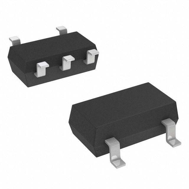
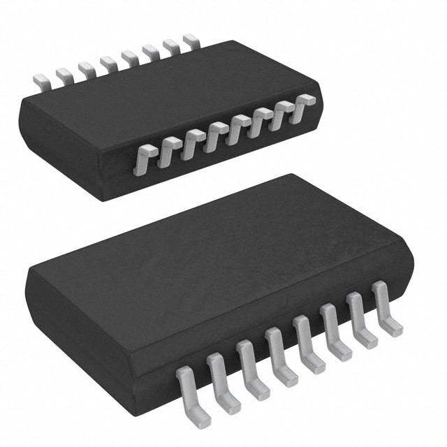
| 供应商器件封装 | 14-TSSOP |
| 共模抑制比—最小值 | 70 dB |
| 关闭 | No Shutdown |
| 其它名称 | 296-28046-5 |
| 包装 | 管件 |
| 压摆率 | 2 V/µs |
| 商标 | Texas Instruments |
| 增益带宽生成 | 5.5 MHz |
| 增益带宽积 | 5.5MHz |
| 安装类型 | 表面贴装 |
| 安装风格 | SMD/SMT |
| 封装 | Tube |
| 封装/外壳 | 14-TSSOP(0.173",4.40mm 宽) |
| 封装/箱体 | TSSOP-14 |
| 工作温度 | -40°C ~ 125°C |
| 工作电源电压 | 2.2 V to 5.5 V |
| 工厂包装数量 | 90 |
| 放大器类型 | 通用 |
| 最大工作温度 | + 125 C |
| 最小工作温度 | - 40 C |
| 标准包装 | 90 |
| 电压-电源,单/双 (±) | 2.2 V ~ 5.5 V, ±1.1 V ~ 2.75 V |
| 电压-输入失调 | 250µV |
| 电流-电源 | 760µA |
| 电流-输入偏置 | 0.2pA |
| 电流-输出/通道 | 50mA |
| 电源电流 | 1.05 mA |
| 电路数 | 4 |
| 系列 | OPA4377 |
| 设计资源 | http://www.digikey.com/product-highlights/cn/zh/texas-instruments-webench-design-center/3176 |
| 转换速度 | 2 V/us |
| 输入偏压电流—最大 | 10 pA |
| 输入补偿电压 | 1 mV |
| 输出电流 | 30 mA |
| 输出类型 | 满摆幅 |
| 通道数量 | 4 Channel |


- 商务部:美国ITC正式对集成电路等产品启动337调查
- 曝三星4nm工艺存在良率问题 高通将骁龙8 Gen1或转产台积电
- 太阳诱电将投资9.5亿元在常州建新厂生产MLCC 预计2023年完工
- 英特尔发布欧洲新工厂建设计划 深化IDM 2.0 战略
- 台积电先进制程称霸业界 有大客户加持明年业绩稳了
- 达到5530亿美元!SIA预计今年全球半导体销售额将创下新高
- 英特尔拟将自动驾驶子公司Mobileye上市 估值或超500亿美元
- 三星加码芯片和SET,合并消费电子和移动部门,撤换高东真等 CEO
- 三星电子宣布重大人事变动 还合并消费电子和移动部门
- 海关总署:前11个月进口集成电路产品价值2.52万亿元 增长14.8%


PDF Datasheet 数据手册内容提取
OPA377 OPA2377 OPA4377 www.ti.com SBOS504B–FEBRUARY2010–REVISEDJANUARY2011 5MHz, Low-Noise, Single, Dual, Quad CMOS Operational Amplifiers CheckforSamples:OPA377,OPA2377,OPA4377 FEATURES DESCRIPTION 1 • GAINBANDWIDTHPRODUCT:5.5MHz The OPA377 family of operational amplifiers are 2 • LOWNOISE:7.5nV/√Hzat1kHz wide-bandwidth CMOS amplifiers that provide very low noise, low input bias current, and low offset • OFFSETVOLTAGE:1mV(max) voltage while operating on a low quiescent current of • INPUTBIASCURRENT:0.2pA 0.76mA(typ). • RAIL-TO-RAILOUTPUT The OPA377 op amps are optimized for low-voltage, • UNITY-GAINSTABLE single-supply applications. The exceptional • EMIINPUTFILTERING combination of ac and dc performance make them ideal for a wide range of applications, including small • QUIESCENTCURRENT:0.76mA/ch signal conditioning, audio, and active filters. In • SUPPLYVOLTAGE:2.2Vto5.5V addition, these parts have a wide supply range with • SMALLPACKAGES: excellent PSRR, making them attractive for SC70,SOT23,andMSOP applications that run directly from batteries without regulation. APPLICATIONS The OPA377 is available in the SC70-5, SOT23-5, • PHOTODIODEPREAMP and SO-8 packages. The dual OPA2377 is offered in • PIEZOELECTRICSENSORPREAMP theSO-8andMSOP-8,andthequadOPA4377inthe TSSOP-14 packages. All versions are specified for • SENSORSIGNALCONDITIONING operationfrom–40°Cto+125°C. • AUDIOEQUIPMENT • ACTIVEFILTERS C INPUT BIAS CURRENT vs TEMPERATURE F 1000 RF 900 800 A) VS nt (p 700 e 600 OPA377 VOUT Curr 500 s Bia 400 ut 300 p n VB I 200 100 0 -50 -25 0 25 50 75 100 125 150 Photodiode Preamplifier Temperature (°C) 1 Pleasebeawarethatanimportantnoticeconcerningavailability,standardwarranty,anduseincriticalapplicationsofTexas Instrumentssemiconductorproductsanddisclaimerstheretoappearsattheendofthisdatasheet. Alltrademarksarethepropertyoftheirrespectiveowners. 2 PRODUCTIONDATAinformationiscurrentasofpublicationdate. ©2010–2011,TexasInstrumentsIncorporated Products conform to specifications per the terms of the Texas Instruments standard warranty. Production processing does not necessarilyincludetestingofallparameters.
OPA377 OPA2377 OPA4377 SBOS504B–FEBRUARY2010–REVISEDJANUARY2011 www.ti.com This integrated circuit can be damaged by ESD. Texas Instruments recommends that all integrated circuits be handled with appropriateprecautions.Failuretoobserveproperhandlingandinstallationprocedurescancausedamage. ESDdamagecanrangefromsubtleperformancedegradationtocompletedevicefailure.Precisionintegratedcircuitsmaybemore susceptibletodamagebecauseverysmallparametricchangescouldcausethedevicenottomeetitspublishedspecifications. ABSOLUTE MAXIMUM RATING(1) Overoperatingfree-airtemperaturerange,unlessotherwisenoted. OPA377,OPA2377,OPA4377 UNIT SupplyVoltage V =(V+)–(V–) +7 V S Voltage(2) (V–)–0.5to(V+)+0.5 V SignalInputTerminals Current(2) ±10 mA OutputShort-Circuit(3) Continuous OperatingTemperature T –40to+150 °C A StorageTemperature T –65to+150 °C A JunctionTemperature T +150 °C J HumanBodyModel 4000 V ESDRating ChargedDeviceModel 1000 V MachineModel 200 V (1) Stressesabovetheseratingsmaycausepermanentdamage.Exposuretoabsolutemaximumconditionsforextendedperiodsmay degradedevicereliability.Thesearestressratingsonly,andfunctionaloperationofthedeviceattheseoranyotherconditionsbeyond thosespecifiedisnotsupported. (2) Inputterminalsarediode-clampedtothepower-supplyrails.Inputsignalsthatcanswingmorethan0.5Vbeyondthesupplyrailsshould becurrentlimitedto10mAorless. (3) Short-circuittoground,oneamplifierperpackage. PACKAGEINFORMATION(1) PRODUCT PACKAGE-LEAD PACKAGEDESIGNATOR PACKAGEMARKING SC70-5 DCK OP377A OPA377 SOT23-5 DBV OP377A SO-8 D OP377A SO-8 D O2377A OPA2377 MSOP-8 DGK OTAQ OPA4377 TSSOP-14 PW O4377A (1) Forthemostcurrentpackageandorderinginformation,seethePackageOptionAddendumattheendofthisdocument,orvisitthe deviceproductfolderatwww.ti.com. 2 SubmitDocumentationFeedback ©2010–2011,TexasInstrumentsIncorporated ProductFolderLink(s):OPA377OPA2377OPA4377
OPA377 OPA2377 OPA4377 www.ti.com SBOS504B–FEBRUARY2010–REVISEDJANUARY2011 ELECTRICAL CHARACTERISTICS: V = +2.2V to +5.5V S Boldfacelimitsapplyoverthespecifiedtemperaturerange:T =–40°Cto+125°C. A AtT =+25°C,R =10kΩconnectedtoV /2,V =V /2,andV =V /2,unlessotherwisenoted. A L S CM S OUT S OPA377,OPA2377,OPA4377 PARAMETERS CONDITIONS MIN TYP MAX UNIT OFFSETVOLTAGE InputOffsetVoltage VOS VS=+5V 0.25 1 mV vsTemperature dVOS/dT –40°Cto+125°C 0.32 2 mV/°C vsPowerSupply PSRR VS=+2.2Vto+5.5V,VCM<(V+)–1.3V 5 28 mV/V OverTemperature VS=+2.2Vto+5.5V,VCM<(V+)–1.3V 5 mV/V ChannelSeparation,dc(dual,quad) 0.5 µV/V INPUTBIASCURRENT InputBiasCurrent IB ±0.2 ±10 pA OverTemperature SeeTypicalCharacteristics pA InputOffsetCurrent IOS ±0.2 ±10 pA NOISE InputVoltageNoise, en f=0.1Hzto10Hz 0.8 mVPP InputVoltageNoiseDensity en f=1kHz 7.5 nV/√Hz InputCurrentNoise in f=1kHz 2 fA/√Hz INPUTVOLTAGERANGE Common-ModeVoltageRange VCM (V–)–0.1 (V+)+0.1 V Common-ModeRejectionRatio CMRR (V–)<VCM<(V+)–1.3V 70 90 dB INPUTCAPACITANCE Differential 6.5 pF Common-Mode 13 pF OPEN-LOOPGAIN Open-LoopVoltageGain AOL 50mV<VO<(V+)–50mV,RL=10kΩ 112 134 dB 100mV<VO<(V+)–100mV,RL=2kΩ 126 dB FREQUENCYRESPONSE VS=5.5V Gain-BandwidthProduct GBW 5.5 MHz SlewRate SR G=+1 2 V/ms SettlingTime0.1% tS 2VStep,G=+1 1.6 ms SettlingTime0.01% tS 2VStep,G=+1 2 ms OverloadRecoveryTime VIN ×Gain>VS 0.33 ms THD+Noise THD+N VO=1VRMS,G=+1,f=1kHz,RL=10kΩ 0.00027 % OUTPUT VoltageOutputSwingfromRail RL=10kΩ 10 20 mV OverTemperature RL=10kΩ 40 mV Short-CircuitCurrent ISC +30/–50 mA CapacitiveLoadDrive CLOAD SeeTypicalCharacteristics Open-LoopOutputImpedance RO 150 Ω POWERSUPPLY SpecifiedVoltageRange VS 2.2 5.5 V QuiescentCurrentperamplifier IQ IO=0,VS=+5.5V 0.76 1.05 mA OverTemperature 1.2 mA TEMPERATURERANGE SpecifiedRange –40 +125 °C ThermalResistance qJA °C/W SC70-5 250 °C/W SOT23-5 200 °C/W MSOP-8,SO-8,TSSOP-14 150 °C/W ©2010–2011,TexasInstrumentsIncorporated SubmitDocumentationFeedback 3 ProductFolderLink(s):OPA377OPA2377OPA4377
OPA377 OPA2377 OPA4377 SBOS504B–FEBRUARY2010–REVISEDJANUARY2011 www.ti.com PIN CONFIGURATIONS OPA377 OPA377 SOT23-5 SO-8 (TOPVIEW) (TOPVIEW) OUT 1 5 V+ NC(1) 1 8 NC(1) V- 2 -IN 2 - 7 V+ + +IN 3 4 -IN +IN 3 6 OUT V- 4 5 NC(1) OPA377 SC70-5 (TOPVIEW) OPA2377 SO-8,MSOP-8 (TOPVIEW) +IN 1 5 V+ V- 2 OUT A 1 8 V+ -IN 3 4 OUT -IN A 2 7 OUT B +IN A 3 6 -IN B V- 4 5 +IN B OPA4377 TSSOP-14 (TOPVIEW) OUT A 1 14 OUT D -IN A 2 13 -IN D +IN A 3 12 +IN D V+ 4 11 V- +IN B 5 10 +IN C -IN B 6 9 -IN C OUT B 7 8 OUT C (1) NCdenotesnointernalconnection. (2) ConnectthermaldietoV–. 4 SubmitDocumentationFeedback ©2010–2011,TexasInstrumentsIncorporated ProductFolderLink(s):OPA377OPA2377OPA4377
OPA377 OPA2377 OPA4377 www.ti.com SBOS504B–FEBRUARY2010–REVISEDJANUARY2011 TYPICAL CHARACTERISTICS AtT =+25°C,V =+5V,R =10kΩconnectedtoV /2,V =V /2,andV =V /2,unlessotherwisenoted. A S L S CM S OUT S POWER-SUPPLYANDCOMMON-MODE OPEN-LOOPGAIN/PHASEvsFREQUENCY REJECTIONRATIOvsFREQUENCY 160 0 120 V(+)Power-Supply Rejection Ratio 140 -20 B) B) 120 Gain -40 atio (d 100 Open-Loop Gain (d 10864200000 Phase -----6811100024000 Phase Margin ()° wer-Supply Rejection R 86420000 V(-)Power-Supply Rejection Ratio CRoemjecmtioonn- MRoadtioe 0 -160 Po -20 -180 0 0.1 1 10 100 1k 10k 100k 1M 10M 10 100 1k 10k 100k 1M 10M Frequency (Hz) Frequency (Hz) Figure1. Figure2. OPEN-LOOPGAINANDPOWER-SUPPLY 0.1Hzto10Hz REJECTIONRATIOvsTEMPERATURE INPUTVOLTAGENOISE 160 dB) Open-Loop Gain (RL= 10kW) R ( 140 R S P and V/div p Gain 120 Powe(rV-SSu=p p2l.y2 VR etoje 5ct.i5oVn) Ratio 500n o o L 100 n- e p O 80 -50 -25 0 25 50 75 100 125 150 1s/div Temperature (°C) Figure3. Figure4. TOTALHARMONICDISTORTION+NOISE INPUTVOLTAGENOISESPECTRALDENSITY vsFREQUENCY 100 1 %) VS= 5V, VCM= 2V, VOUT= 1VRMS e ( s Ö)Hz + Noi 0.1 V/ n e (n ortio ge Nois 10 nic Dist 0.01 Gain = 10V/V a o Volt arm 0.001 al H Gain = 1V/V Tot 1 0.0001 1 10 100 1k 10k 100k 10 100 1k 10k 100k Frequency (Hz) Frequency (Hz) Figure5. Figure6. ©2010–2011,TexasInstrumentsIncorporated SubmitDocumentationFeedback 5 ProductFolderLink(s):OPA377OPA2377OPA4377
OPA377 OPA2377 OPA4377 SBOS504B–FEBRUARY2010–REVISEDJANUARY2011 www.ti.com TYPICAL CHARACTERISTICS (continued) AtT =+25°C,V =+5V,R =10kΩconnectedtoV /2,V =V /2,andV =V /2,unlessotherwisenoted. A S L S CM S OUT S COMMON-MODEREJECTIONRATIO QUIESCENTCURRENT vsTEMPERATURE vsTEMPERATURE 110 1000 B) d atio ( 100 A) 900 R m on 90 nt ( ejecti 80 Curre 800 Mode R 70 escent 700 n- ui o Q m 600 m 60 o C 50 500 -50 -25 0 25 50 75 100 125 150 -50 -25 0 25 50 75 100 125 150 Temperature (°C) Temperature (°C) Figure7. Figure8. QUIESCENTANDSHORT-CIRCUITCURRENT SHORT-CIRCUITCURRENT vsSUPPLYVOLTAGE vsTEMPERATURE 1000 50 75 V =±2.75V S 50 900 40 S A) I muiescent Current (A) 870000 IQ ISC+ 3200 hort-Circuit Current (m hort-Circuit Current (m --2255500 ISSCC-+ Q 600 10 A S ) -75 500 0 -100 2.0 2.5 3.0 3.5 4.0 4.5 5.0 5.5 -50 -25 0 25 50 75 100 125 150 Supply Voltage (V) Temperature (°C) Figure9. Figure10. INPUTBIASCURRENTvsTEMPERATURE OUTPUTVOLTAGEvsOUTPUTCURRENT 1000 3 V =±2.75 900 S 2 800 A) ent (p 760000 ge (V) 1 +150°C +125°C +25°C -40°C ut Bias Curr 543000000 Output Volta -01 p n I 200 -2 100 0 -3 -50 -25 0 25 50 75 100 125 150 0 10 20 30 40 50 60 70 80 Temperature (°C) Output Current (mA) Figure11. Figure12. 6 SubmitDocumentationFeedback ©2010–2011,TexasInstrumentsIncorporated ProductFolderLink(s):OPA377OPA2377OPA4377
OPA377 OPA2377 OPA4377 www.ti.com SBOS504B–FEBRUARY2010–REVISEDJANUARY2011 TYPICAL CHARACTERISTICS (continued) AtT =+25°C,V =+5V,R =10kΩconnectedtoV /2,V =V /2,andV =V /2,unlessotherwisenoted. A S L S CM S OUT S OFFSETVOLTAGE PRODUCTIONDISTRIBUTION MAXIMUMOUTPUTVOLTAGEvsFREQUENCY 6 V = 5.5V S V = 5V 5 S )P VP 4 Population ut Voltage ( 3 VS= 2.5V utp 2 O 1 0 00000000000000000000000000000000000000000 1k 10k 100k 1M 10M 0987654321 1234567890 1--------- 1 - Frequency (Hz) Offset Voltage (mV) Figure13. Figure14. SMALL-SIGNALOVERSHOOTvsLOADCAPACITANCE SMALL-SIGNALPULSERESPONSE 50 G = +1V/V G = +1 R = 10kW L %) 40 C = 50pF ot ( L o h ers 30 div Ov V/ al 0m n 20 5 g Si all- m 10 S 0 10 100 1k Time (400ns/div) Load Capacitance (pF) Figure15. Figure16. LARGE-SIGNALPULSERESPONSE SETTLINGTIMEvsCLOSED-LOOPGAIN 100 G = +1 R = 2kW L C = 50pF L ms) 10 1V/div g Time ( 0.01% n ettli 1 S 0.1% 0.1 Time (2ms/div) 1 10 100 Closed-Loop Gain (V/V) Figure17. Figure18. ©2010–2011,TexasInstrumentsIncorporated SubmitDocumentationFeedback 7 ProductFolderLink(s):OPA377OPA2377OPA4377
OPA377 OPA2377 OPA4377 SBOS504B–FEBRUARY2010–REVISEDJANUARY2011 www.ti.com TYPICAL CHARACTERISTICS (continued) AtT =+25°C,V =+5V,R =10kΩconnectedtoV /2,V =V /2,andV =V /2,unlessotherwisenoted. A S L S CM S OUT S CHANNELSEPARATIONvsFREQUENCY OPEN-LOOPOUTPUTRESISTANCEvsFREQUENCY 140 1k W) on (dB) 112000 sistance ( 100 ati 80 Re par ut 10 e p S 60 ut 400mA Load nel p O han 40 Loo 1 2mA Load C n- 20 pe O 0 0.1 10 100 1k 10k 100k 1M 10M 100M 10 100 1k 10k 100k 1M 10M Frequency (Hz) Frequency (Hz) Figure19. Figure20. 8 SubmitDocumentationFeedback ©2010–2011,TexasInstrumentsIncorporated ProductFolderLink(s):OPA377OPA2377OPA4377
OPA377 OPA2377 OPA4377 www.ti.com SBOS504B–FEBRUARY2010–REVISEDJANUARY2011 APPLICATION INFORMATION OPERATING CHARACTERISTICS R 2 10kW The OPA377 family of amplifiers has parameters that are fully specified from 2.2V to 5.5V (±1.1V to ±2.75V). Many of the specifications apply from –40°C +5V to +125°C. Parameters that can exhibit significant variance with regard to operating voltage or temperature are presented in the Typical C1 100nF Characteristics. R 1 1kW GENERAL LAYOUT GUIDELINES OPA377 V OUT For best operational performance of the device, good V printed circuit board (PCB) layout practices are IN required. Low-loss, 0.1mF bypass capacitors must be connected between each supply pin and ground, placed as close to the device as possible. A single V = 2.5V CM bypass capacitor from V+ to ground is applicable to single-supplyapplications. BASIC AMPLIFIER CONFIGURATIONS Figure21. BasicSingle-SupplyConnection The OPA377 family is unity-gain stable. It does not exhibit output phase inversion when the input is overdriven. A typical single-supply connection is COMMON-MODE VOLTAGE RANGE shown in Figure 21. The OPA377 is configured as a basic inverting amplifier with a gain of –10V/V. This The input common-mode voltage range of the single-supply connection has an output centered on OPA377 series extends 100mV beyond the supply the common-mode voltage, V . For the circuit rails. The offset voltage of the amplifier is low, from CM shown, this voltage is 2.5V, but may be any value approximately (V–) to (V+) – 1V, as shown in withinthecommon-modeinputvoltagerange. Figure 22. The offset voltage increases as common-mode voltage exceeds (V+) –1V. Common-mode rejection is specified from (V–) to (V+)– 1.3V. 3 2 V) m e ( 1 g a olt V 0 et s Off -1 ut p n I -2 -V +V -3 -0.5 0 0.5 1.0 1.5 2.0 2.5 3.0 3.5 4.0 4.5 5.0 5.5 6.0 Input Common-Mode Voltage (V) Figure22. OffsetandCommon-ModeVoltage ©2010–2011,TexasInstrumentsIncorporated SubmitDocumentationFeedback 9 ProductFolderLink(s):OPA377OPA2377OPA4377
OPA377 OPA2377 OPA4377 SBOS504B–FEBRUARY2010–REVISEDJANUARY2011 www.ti.com INPUT AND ESD PROTECTION CAPACITIVE LOAD AND STABILITY The OPA377 family incorporates internal electrostatic The OPA377 series of amplifiers may be used in discharge (ESD) protection circuits on all pins. In the applications where driving a capacitive load is case of input and output pins, this protection primarily required. As with all op amps, there may be specific consists of current steering diodes connected instances where the OPAx377 can become unstable, betweentheinputandpower-supplypins.TheseESD leading to oscillation. The particular op amp circuit protection diodes also provide in-circuit, input configuration, layout, gain, and output loading are overdrive protection, as long as the current is limited some of the factors to consider when establishing to 10mA as stated in the Absolute Maximum Ratings. whether an amplifier will be stable in operation. An op Figure 23 shows how a series input resistor may be amp in the unity-gain (+1V/V) buffer configuration and added to the driven input to limit the input current. driving a capacitive load exhibits a greater tendency The added resistor contributes thermal noise at the to be unstable than an amplifier operated at a higher amplifier input and its value should be kept to a noise gain. The capacitive load, in conjunction with minimuminnoise-sensitiveapplications. the op amp output resistance, creates a pole within the feedback loop that degrades the phase margin. The degradation of the phase margin increases as V+ thecapacitiveloadingincreases. I The OPAx377 in a unity-gain configuration can OVERLOAD 10mA max directly drive up to 250pF pure capacitive load. OPA377 V OUT Increasing the gain enhances the ability of the V IN 5kW amplifier to drive greater capacitive loads; see the typical characteristic plot, Small-Signal Overshoot vs Capacitive Load. In unity-gain configurations, Figure23. InputCurrentProtection capacitive load drive can be improved by inserting a small (10Ω to 20Ω) resistor, R , in series with the S output, as shown in Figure 24. This resistor EMI SUSCEPTIBILITY AND INPUT FILTERING significantly reduces ringing while maintaining dc performance for purely capacitive loads. However, if Operational amplifiers vary in susceptibility to there is a resistive load in parallel with the capacitive electromagnetic interference (EMI). If conducted EMI load, a voltage divider is created, introducing a gain enters the operational amplifier, the dc offset error at the output and slightly reducing the output observed at the amplifier output may shift from the swing. The error introduced is proportional to the ratio nominal value while the EMI is present. This shift is a R /R , and is generally negligible at low output result of signal rectification associated with the S L currentlevels. internal semiconductor junctions. While all amplifier pin functions can be affected by EMI, the input pins are likely to be the most susceptible. The OPA377 V+ operational amplifier family incorporates an internal input low-pass filter that reduces the amplifier R S response to EMI. Both common-mode and differential OPA377 V OUT mode filtering are provided by the input filter. The V 10Wto filter is designed for a cutoff frequency of IN 20W RL CL approximately 75MHz (–3dB), with a roll-off of 20dB perdecade. Figure24. ImprovingCapacitiveLoadDrive 10 SubmitDocumentationFeedback ©2010–2011,TexasInstrumentsIncorporated ProductFolderLink(s):OPA377OPA2377OPA4377
OPA377 OPA2377 OPA4377 www.ti.com SBOS504B–FEBRUARY2010–REVISEDJANUARY2011 ACTIVE FILTERING DRIVING AN ANALOG-TO-DIGITAL CONVERTER The OPA377 series is well-suited for filter applications requiring a wide bandwidth, fast slew The low noise and wide gain bandwidth of the rate, low-noise, single-supply operational amplifier. OPA377 family make it an ideal driver for ADCs. Figure 25 shows a 50kHz, 2nd-order, low-pass filter. Figure 26 illustrates the OPA377 driving an The components have been selected to provide a ADS8327,16-bit,250kSPSconverter.Theamplifieris maximally-flat Butterworth response. Beyond the connectedasaunity-gain,noninvertingbuffer. cutoff frequency, roll-off is –40dB/dec. The Butterworth response is ideal for applications +5V requiring predictable gain characteristics such as the anti-aliasing filter used ahead of an analog-to-digital C converter(ADC). 1 0.1mF +5V R(1) 1 R 100W 3 +IN 5.49kW OPA377 ADS8327 Low Power C2 VIN 1.C23n(1F) -IN 50106k-SBPitS 150pF REF IN +5V V+ R R 5.491kW 12.42kW REF5040 4.096V C4 100nF OPA377 V C OUT 1 1nF V IN (1) Suggested value; may require adjustment based on specific application. (2) Initialcalibrationrecommended. Figure26. DrivinganADS8327(2) (V+)/2 Figure25. Second-OrderButterworth50kHz Low-PassFilter ©2010–2011,TexasInstrumentsIncorporated SubmitDocumentationFeedback 11 ProductFolderLink(s):OPA377OPA2377OPA4377
OPA377 OPA2377 OPA4377 SBOS504B–FEBRUARY2010–REVISEDJANUARY2011 www.ti.com REVISION HISTORY NOTE:Pagenumbersforpreviousrevisionsmaydifferfrompagenumbersinthecurrentversion. ChangesfromRevisionA(October2010)toRevisionB Page • Changeddocumentstatustoproductiondata ...................................................................................................................... 1 • Deletedcross-referencetonote2andshadingfromDCKpackageinPackageInformationtable ..................................... 2 • UpdatedFigure22 ................................................................................................................................................................ 9 ChangesfromOriginal(February2010)toRevisionA Page • DeletedDFNfromlistofpackagesinfinalFeaturesbullet .................................................................................................. 1 • DeletedDFNpackagefromDescriptionsection ................................................................................................................... 1 • UpdatedInputBiasCurrentvsTemperatureplot ................................................................................................................. 1 • Deletedcross-referencetonote2andshadingfromallpackagesexceptSC70-5inPackageInformationtable .............. 2 • DeletedDFN-8packagefromPackageInformationtable .................................................................................................... 2 • DeletedTemperatureRange,DFN-8parameterfromElectricalCharacteristicstable ........................................................ 3 • DeletedDFN-8pinconfiguration .......................................................................................................................................... 4 • UpdatedFigure11 ................................................................................................................................................................ 6 12 SubmitDocumentationFeedback ©2010–2011,TexasInstrumentsIncorporated ProductFolderLink(s):OPA377OPA2377OPA4377
PACKAGE OPTION ADDENDUM www.ti.com 6-Feb-2020 PACKAGING INFORMATION Orderable Device Status Package Type Package Pins Package Eco Plan Lead/Ball Finish MSL Peak Temp Op Temp (°C) Device Marking Samples (1) Drawing Qty (2) (6) (3) (4/5) OPA2377AID ACTIVE SOIC D 8 75 Green (RoHS NIPDAU Level-2-260C-1 YEAR -40 to 125 O2377A & no Sb/Br) OPA2377AIDGKR ACTIVE VSSOP DGK 8 2500 Green (RoHS NIPDAU | NIPDAUAG Level-2-260C-1 YEAR -40 to 125 OTAQ & no Sb/Br) OPA2377AIDGKT ACTIVE VSSOP DGK 8 250 Green (RoHS NIPDAU | NIPDAUAG Level-2-260C-1 YEAR -40 to 125 OTAQ & no Sb/Br) OPA2377AIDR ACTIVE SOIC D 8 2500 Green (RoHS NIPDAU Level-2-260C-1 YEAR -40 to 125 O2377A & no Sb/Br) OPA377AID ACTIVE SOIC D 8 75 Green (RoHS NIPDAU Level-2-260C-1 YEAR -40 to 125 OP377A & no Sb/Br) OPA377AIDBVR ACTIVE SOT-23 DBV 5 3000 Green (RoHS NIPDAU Level-2-260C-1 YEAR -40 to 125 PAG & no Sb/Br) OPA377AIDBVT ACTIVE SOT-23 DBV 5 250 Green (RoHS NIPDAU Level-2-260C-1 YEAR -40 to 125 PAG & no Sb/Br) OPA377AIDCKR ACTIVE SC70 DCK 5 3000 Green (RoHS NIPDAU Level-2-260C-1 YEAR -40 to 125 PAF & no Sb/Br) OPA377AIDCKT ACTIVE SC70 DCK 5 250 Green (RoHS NIPDAU Level-2-260C-1 YEAR -40 to 125 PAF & no Sb/Br) OPA377AIDR ACTIVE SOIC D 8 2500 Green (RoHS NIPDAU Level-2-260C-1 YEAR -40 to 125 OP377A & no Sb/Br) OPA4377AIPW ACTIVE TSSOP PW 14 90 Green (RoHS NIPDAU Level-2-260C-1 YEAR -40 to 125 OP4377A & no Sb/Br) OPA4377AIPWR ACTIVE TSSOP PW 14 2000 Green (RoHS NIPDAU Level-2-260C-1 YEAR -40 to 125 OP4377A & no Sb/Br) (1) The marketing status values are defined as follows: ACTIVE: Product device recommended for new designs. LIFEBUY: TI has announced that the device will be discontinued, and a lifetime-buy period is in effect. NRND: Not recommended for new designs. Device is in production to support existing customers, but TI does not recommend using this part in a new design. PREVIEW: Device has been announced but is not in production. Samples may or may not be available. OBSOLETE: TI has discontinued the production of the device. (2) RoHS: TI defines "RoHS" to mean semiconductor products that are compliant with the current EU RoHS requirements for all 10 RoHS substances, including the requirement that RoHS substance do not exceed 0.1% by weight in homogeneous materials. Where designed to be soldered at high temperatures, "RoHS" products are suitable for use in specified lead-free processes. TI may reference these types of products as "Pb-Free". RoHS Exempt: TI defines "RoHS Exempt" to mean products that contain lead but are compliant with EU RoHS pursuant to a specific EU RoHS exemption. Addendum-Page 1
PACKAGE OPTION ADDENDUM www.ti.com 6-Feb-2020 Green: TI defines "Green" to mean the content of Chlorine (Cl) and Bromine (Br) based flame retardants meet JS709B low halogen requirements of <=1000ppm threshold. Antimony trioxide based flame retardants must also meet the <=1000ppm threshold requirement. (3) MSL, Peak Temp. - The Moisture Sensitivity Level rating according to the JEDEC industry standard classifications, and peak solder temperature. (4) There may be additional marking, which relates to the logo, the lot trace code information, or the environmental category on the device. (5) Multiple Device Markings will be inside parentheses. Only one Device Marking contained in parentheses and separated by a "~" will appear on a device. If a line is indented then it is a continuation of the previous line and the two combined represent the entire Device Marking for that device. (6) Lead/Ball Finish - Orderable Devices may have multiple material finish options. Finish options are separated by a vertical ruled line. Lead/Ball Finish values may wrap to two lines if the finish value exceeds the maximum column width. Important Information and Disclaimer:The information provided on this page represents TI's knowledge and belief as of the date that it is provided. TI bases its knowledge and belief on information provided by third parties, and makes no representation or warranty as to the accuracy of such information. Efforts are underway to better integrate information from third parties. TI has taken and continues to take reasonable steps to provide representative and accurate information but may not have conducted destructive testing or chemical analysis on incoming materials and chemicals. TI and TI suppliers consider certain information to be proprietary, and thus CAS numbers and other limited information may not be available for release. In no event shall TI's liability arising out of such information exceed the total purchase price of the TI part(s) at issue in this document sold by TI to Customer on an annual basis. OTHER QUALIFIED VERSIONS OF OPA2377, OPA377, OPA4377 : •Automotive: OPA2377-Q1, OPA377-Q1, OPA4377-Q1 NOTE: Qualified Version Definitions: •Automotive - Q100 devices qualified for high-reliability automotive applications targeting zero defects Addendum-Page 2
PACKAGE MATERIALS INFORMATION www.ti.com 8-May-2018 TAPE AND REEL INFORMATION *Alldimensionsarenominal Device Package Package Pins SPQ Reel Reel A0 B0 K0 P1 W Pin1 Type Drawing Diameter Width (mm) (mm) (mm) (mm) (mm) Quadrant (mm) W1(mm) OPA2377AIDGKR VSSOP DGK 8 2500 330.0 12.4 5.3 3.4 1.4 8.0 12.0 Q1 OPA2377AIDGKT VSSOP DGK 8 250 330.0 12.4 5.3 3.4 1.4 8.0 12.0 Q1 OPA2377AIDR SOIC D 8 2500 330.0 12.4 6.4 5.2 2.1 8.0 12.0 Q1 OPA377AIDBVR SOT-23 DBV 5 3000 180.0 8.4 3.23 3.17 1.37 4.0 8.0 Q3 OPA377AIDBVR SOT-23 DBV 5 3000 180.0 8.4 3.2 3.2 1.4 4.0 8.0 Q3 OPA377AIDBVT SOT-23 DBV 5 250 180.0 8.4 3.23 3.17 1.37 4.0 8.0 Q3 OPA377AIDBVT SOT-23 DBV 5 250 179.0 8.4 3.2 3.2 1.4 4.0 8.0 Q3 OPA377AIDCKR SC70 DCK 5 3000 179.0 8.4 2.2 2.5 1.2 4.0 8.0 Q3 OPA377AIDCKT SC70 DCK 5 250 179.0 8.4 2.2 2.5 1.2 4.0 8.0 Q3 OPA377AIDR SOIC D 8 2500 330.0 12.4 6.4 5.2 2.1 8.0 12.0 Q1 OPA4377AIPWR TSSOP PW 14 2000 330.0 12.4 6.9 5.6 1.6 8.0 12.0 Q1 PackMaterials-Page1
PACKAGE MATERIALS INFORMATION www.ti.com 8-May-2018 *Alldimensionsarenominal Device PackageType PackageDrawing Pins SPQ Length(mm) Width(mm) Height(mm) OPA2377AIDGKR VSSOP DGK 8 2500 366.0 364.0 50.0 OPA2377AIDGKT VSSOP DGK 8 250 366.0 364.0 50.0 OPA2377AIDR SOIC D 8 2500 367.0 367.0 35.0 OPA377AIDBVR SOT-23 DBV 5 3000 223.0 270.0 35.0 OPA377AIDBVR SOT-23 DBV 5 3000 195.0 200.0 45.0 OPA377AIDBVT SOT-23 DBV 5 250 223.0 270.0 35.0 OPA377AIDBVT SOT-23 DBV 5 250 195.0 200.0 45.0 OPA377AIDCKR SC70 DCK 5 3000 195.0 200.0 45.0 OPA377AIDCKT SC70 DCK 5 250 195.0 200.0 45.0 OPA377AIDR SOIC D 8 2500 367.0 367.0 35.0 OPA4377AIPWR TSSOP PW 14 2000 367.0 367.0 35.0 PackMaterials-Page2
None
None
PACKAGE OUTLINE DBV0005A SOT-23 - 1.45 mm max height SCALE 4.000 SMALL OUTLINE TRANSISTOR C 3.0 2.6 0.1 C 1.75 1.45 1.45 B A 0.90 PIN 1 INDEX AREA 1 5 2X 0.95 3.05 2.75 1.9 1.9 2 4 3 0.5 5X 0.3 0.15 0.2 C A B (1.1) TYP 0.00 0.25 GAGE PLANE 0.22 TYP 0.08 8 TYP 0.6 0 0.3 TYP SEATING PLANE 4214839/E 09/2019 NOTES: 1. All linear dimensions are in millimeters. Any dimensions in parenthesis are for reference only. Dimensioning and tolerancing per ASME Y14.5M. 2. This drawing is subject to change without notice. 3. Refernce JEDEC MO-178. 4. Body dimensions do not include mold flash, protrusions, or gate burrs. Mold flash, protrusions, or gate burrs shall not exceed 0.15 mm per side. www.ti.com
EXAMPLE BOARD LAYOUT DBV0005A SOT-23 - 1.45 mm max height SMALL OUTLINE TRANSISTOR PKG 5X (1.1) 1 5 5X (0.6) SYMM (1.9) 2 2X (0.95) 3 4 (R0.05) TYP (2.6) LAND PATTERN EXAMPLE EXPOSED METAL SHOWN SCALE:15X SOLDER MASK SOLDER MASK METAL UNDER METAL OPENING OPENING SOLDER MASK EXPOSED METAL EXPOSED METAL 0.07 MAX 0.07 MIN ARROUND ARROUND NON SOLDER MASK SOLDER MASK DEFINED DEFINED (PREFERRED) SOLDER MASK DETAILS 4214839/E 09/2019 NOTES: (continued) 5. Publication IPC-7351 may have alternate designs. 6. Solder mask tolerances between and around signal pads can vary based on board fabrication site. www.ti.com
EXAMPLE STENCIL DESIGN DBV0005A SOT-23 - 1.45 mm max height SMALL OUTLINE TRANSISTOR PKG 5X (1.1) 1 5 5X (0.6) SYMM 2 (1.9) 2X(0.95) 3 4 (R0.05) TYP (2.6) SOLDER PASTE EXAMPLE BASED ON 0.125 mm THICK STENCIL SCALE:15X 4214839/E 09/2019 NOTES: (continued) 7. Laser cutting apertures with trapezoidal walls and rounded corners may offer better paste release. IPC-7525 may have alternate design recommendations. 8. Board assembly site may have different recommendations for stencil design. www.ti.com
None
None
PACKAGE OUTLINE D0008A SOIC - 1.75 mm max height SCALE 2.800 SMALL OUTLINE INTEGRATED CIRCUIT C SEATING PLANE .228-.244 TYP [5.80-6.19] .004 [0.1] C A PIN 1 ID AREA 6X .050 [1.27] 8 1 2X .189-.197 [4.81-5.00] .150 NOTE 3 [3.81] 4X (0 -15 ) 4 5 8X .012-.020 B .150-.157 [0.31-0.51] .069 MAX [3.81-3.98] .010 [0.25] C A B [1.75] NOTE 4 .005-.010 TYP [0.13-0.25] 4X (0 -15 ) SEE DETAIL A .010 [0.25] .004-.010 0 - 8 [0.11-0.25] .016-.050 [0.41-1.27] DETAIL A (.041) TYPICAL [1.04] 4214825/C 02/2019 NOTES: 1. Linear dimensions are in inches [millimeters]. Dimensions in parenthesis are for reference only. Controlling dimensions are in inches. Dimensioning and tolerancing per ASME Y14.5M. 2. This drawing is subject to change without notice. 3. This dimension does not include mold flash, protrusions, or gate burrs. Mold flash, protrusions, or gate burrs shall not exceed .006 [0.15] per side. 4. This dimension does not include interlead flash. 5. Reference JEDEC registration MS-012, variation AA. www.ti.com
EXAMPLE BOARD LAYOUT D0008A SOIC - 1.75 mm max height SMALL OUTLINE INTEGRATED CIRCUIT 8X (.061 ) [1.55] SYMM SEE DETAILS 1 8 8X (.024) [0.6] SYMM (R.002 ) TYP [0.05] 5 4 6X (.050 ) [1.27] (.213) [5.4] LAND PATTERN EXAMPLE EXPOSED METAL SHOWN SCALE:8X SOLDER MASK SOLDER MASK METAL OPENING OPENING METAL UNDER SOLDER MASK EXPOSED METAL EXPOSED METAL .0028 MAX .0028 MIN [0.07] [0.07] ALL AROUND ALL AROUND NON SOLDER MASK SOLDER MASK DEFINED DEFINED SOLDER MASK DETAILS 4214825/C 02/2019 NOTES: (continued) 6. Publication IPC-7351 may have alternate designs. 7. Solder mask tolerances between and around signal pads can vary based on board fabrication site. www.ti.com
EXAMPLE STENCIL DESIGN D0008A SOIC - 1.75 mm max height SMALL OUTLINE INTEGRATED CIRCUIT 8X (.061 ) [1.55] SYMM 1 8 8X (.024) [0.6] SYMM (R.002 ) TYP [0.05] 5 4 6X (.050 ) [1.27] (.213) [5.4] SOLDER PASTE EXAMPLE BASED ON .005 INCH [0.125 MM] THICK STENCIL SCALE:8X 4214825/C 02/2019 NOTES: (continued) 8. Laser cutting apertures with trapezoidal walls and rounded corners may offer better paste release. IPC-7525 may have alternate design recommendations. 9. Board assembly site may have different recommendations for stencil design. www.ti.com
None
None
IMPORTANTNOTICEANDDISCLAIMER TI PROVIDES TECHNICAL AND RELIABILITY DATA (INCLUDING DATASHEETS), DESIGN RESOURCES (INCLUDING REFERENCE DESIGNS), APPLICATION OR OTHER DESIGN ADVICE, WEB TOOLS, SAFETY INFORMATION, AND OTHER RESOURCES “AS IS” AND WITH ALL FAULTS, AND DISCLAIMS ALL WARRANTIES, EXPRESS AND IMPLIED, INCLUDING WITHOUT LIMITATION ANY IMPLIED WARRANTIES OF MERCHANTABILITY, FITNESS FOR A PARTICULAR PURPOSE OR NON-INFRINGEMENT OF THIRD PARTY INTELLECTUAL PROPERTY RIGHTS. These resources are intended for skilled developers designing with TI products. You are solely responsible for (1) selecting the appropriate TI products for your application, (2) designing, validating and testing your application, and (3) ensuring your application meets applicable standards, and any other safety, security, or other requirements. These resources are subject to change without notice. TI grants you permission to use these resources only for development of an application that uses the TI products described in the resource. Other reproduction and display of these resources is prohibited. No license is granted to any other TI intellectual property right or to any third party intellectual property right. TI disclaims responsibility for, and you will fully indemnify TI and its representatives against, any claims, damages, costs, losses, and liabilities arising out of your use of these resources. TI’s products are provided subject to TI’s Terms of Sale (www.ti.com/legal/termsofsale.html) or other applicable terms available either on ti.com or provided in conjunction with such TI products. TI’s provision of these resources does not expand or otherwise alter TI’s applicable warranties or warranty disclaimers for TI products. Mailing Address: Texas Instruments, Post Office Box 655303, Dallas, Texas 75265 Copyright © 2020, Texas Instruments Incorporated