ICGOO在线商城 > OPA4243EA/250

 Datasheet下载
- 型号: OPA4243EA/250
- 制造商: Texas Instruments
- 库位|库存: xxxx|xxxx
- 要求:
| 数量阶梯 | 香港交货 | 国内含税 |
| +xxxx | $xxxx | ¥xxxx |
查看当月历史价格
查看今年历史价格
OPA4243EA/250产品简介:
ICGOO电子元器件商城为您提供OPA4243EA/250由Texas Instruments设计生产,在icgoo商城现货销售,并且可以通过原厂、代理商等渠道进行代购。 提供OPA4243EA/250价格参考¥22.60-¥41.98以及Texas InstrumentsOPA4243EA/250封装/规格参数等产品信息。 你可以下载OPA4243EA/250参考资料、Datasheet数据手册功能说明书, 资料中有OPA4243EA/250详细功能的应用电路图电压和使用方法及教程。
| 参数 | 数值 |
| -3db带宽 | - |
| 产品目录 | 集成电路 (IC)半导体 |
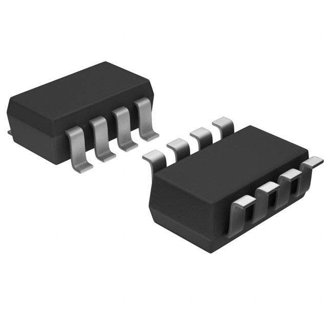
| 描述 | IC OPAMP GP 430KHZ 14TSSOP运算放大器 - 运放 Quad MicroPower Single-Supply |
| 产品分类 | Linear - Amplifiers - Instrumentation, OP Amps, Buffer Amps集成电路 - IC |
| 品牌 | Texas Instruments |
| 产品手册 | http://www.ti.com/litv/sbos118 |
| 产品图片 |
|
| rohs | 符合RoHS无铅 / 符合限制有害物质指令(RoHS)规范要求 |
| 产品系列 | 放大器 IC,运算放大器 - 运放,Texas Instruments OPA4243EA/250- |
| 数据手册 | |
| 产品型号 | OPA4243EA/250 |
| 产品目录页面 | |
| 产品种类 | 运算放大器 - 运放 |
| 供应商器件封装 | 14-TSSOP |
| 共模抑制比—最小值 | 82 dB |
| 关闭 | No Shutdown |
| 其它名称 | OPA4243EACT |
| 包装 | 剪切带 (CT) |
| 压摆率 | 0.16 V/µs |
| 双重电源电压 | +/- 3 V, +/- 5 V, +/- 9 V |
| 商标 | Texas Instruments |
| 增益带宽生成 | 0.43 MHz |
| 增益带宽积 | 430kHz |
| 安装类型 | 表面贴装 |
| 安装风格 | SMD/SMT |
| 封装 | Reel |
| 封装/外壳 | 14-TSSOP(0.173",4.40mm 宽) |
| 封装/箱体 | TSSOP-14 |
| 工作温度 | -40°C ~ 85°C |
| 工作电源电压 | 2.2 V to 36 V, +/- 1.1 V to +/- 18 V |
| 工厂包装数量 | 250 |
| 放大器类型 | 通用 |
| 最大双重电源电压 | +/- 18 V |
| 最大工作温度 | + 85 C |
| 最小双重电源电压 | +/- 1.1 V |
| 最小工作温度 | - 40 C |
| 标准包装 | 1 |
| 电压-电源,单/双 (±) | 2.2 V ~ 36 V, ±1.1 V ~ 18 V |
| 电压-输入失调 | 2mV |
| 电流-电源 | 45µA |
| 电流-输入偏置 | 10nA |
| 电流-输出/通道 | 25mA |
| 电源电流 | 0.24 mA |
| 电路数 | 4 |
| 系列 | OPA4243 |
| 设计资源 | http://www.digikey.com/product-highlights/cn/zh/texas-instruments-webench-design-center/3176 |
| 转换速度 | 0.16 V/us |
| 输入偏压电流—最大 | 25 nA |
| 输入参考电压噪声 | 22 nV |
| 输入补偿电压 | 5 mV |
| 输出类型 | - |
| 通道数量 | 4 Channel |


- 商务部:美国ITC正式对集成电路等产品启动337调查
- 曝三星4nm工艺存在良率问题 高通将骁龙8 Gen1或转产台积电
- 太阳诱电将投资9.5亿元在常州建新厂生产MLCC 预计2023年完工
- 英特尔发布欧洲新工厂建设计划 深化IDM 2.0 战略
- 台积电先进制程称霸业界 有大客户加持明年业绩稳了
- 达到5530亿美元!SIA预计今年全球半导体销售额将创下新高
- 英特尔拟将自动驾驶子公司Mobileye上市 估值或超500亿美元
- 三星加码芯片和SET,合并消费电子和移动部门,撤换高东真等 CEO
- 三星电子宣布重大人事变动 还合并消费电子和移动部门
- 海关总署:前11个月进口集成电路产品价值2.52万亿元 增长14.8%


PDF Datasheet 数据手册内容提取
® OPA4243 OPA4243® OPA4243® For most current data sheet and other product information, visit www.burr-brown.com Quad OPERATIONAL AMPLIFIER MicroPOWER, Single-Supply FEATURES DESCRIPTION l MICRO-SIZE, TSSOP PACKAGE The OPA4243 is a four-channel op amp specifically l SINGLE-SUPPLY OPERATION designed for high density, space-limited applications, such as LCD bias drivers, PCMCIA cards, battery- l WIDE SUPPLY RANGE: 2.2V to 36V packs and portable instruments. In addition to small l LOW QUIESCENT CURRENT: 45m A/chan size, this part features wide output swing, very low l WIDE BANDWIDTH: 430kHz quiescent current, and low bias current. Other features l WIDE INPUT/OUTPUT SWING include unity gain stability and the best speed power ratio available. Power supplies in the range of 2.2V to 36V (– 1.1V to – 18V) can be used. APPLICATIONS Each channel uses completely independent circuitry l LCD DISPLAY DRIVERS for lowest crosstalk and freedom from interaction, l BATTERY POWERED SYSTEMS even when overloaded. In addition, the amplifier is free from output inversion when the inputs are driven l PORTABLE EQUIPMENT to the rail. The OPA4243EA is supplied in the minia- l PCMCIA CARDS ture TSSOP-14 surface mount package. Specifications l BATTERY PACKS AND POWER SUPPLIES apply from –40(cid:176) C to +85(cid:176) C. However, as the exten- l CONSUMER PRODUCTS sive typical performance curves indicate, the OPA4243 can be used over the full –55(cid:176) C to +125(cid:176) C range. A SPICE macromodel is available for design analysis. OPA4243EA Output A 1 14 Output D –Input A 2 13 –Input D +Input A 3 12 +Input D +V 4 11 –V +Input B 5 10 +Input C –Input B 6 9 –Input C Output B 7 8 Output C TSSOP-14 International Airport Industrial Park • Mailing Address: PO Box 11400, Tucson, AZ 85734 • Street Address: 6730 S. Tucson Blvd., Tucson, AZ 85706 • Tel: (520) 746-1111 Twx: 910-952-1111 • Internet: http://www.burr-brown.com/ • Cable: BBRCORP • Telex: 066-6491 • FAX: (520) 889-1510 • Immediate Product Info: (800) 548-6132 ® © 1999 Burr-Brown Corporation PDS-11562A PrOintePd iAn U4.S2.A4. N3ovember, 1999 SBOS118
SPECIFICATIONS: V = +2.6V to +36V S (cid:176) (cid:176) Boldface limits apply over the specified temperature range, T = –40 C to +85 C A At T = +25(cid:176)C, R = 20kW connected to ground, unless otherwise noted. A L OPA4243EA PARAMETER CONDITIONS MIN TYP(1) MAX UNITS OFFSET VOLTAGE Input Offset Voltage V V = – 7.5V, V = 0 – 2 – 5 mV OS S CM Over Temperature – 6 mV vs Temperature dV /dT T = –40(cid:176)C to +85(cid:176)C – 2.5 m V/(cid:176)C OS A vs Power Supply PSRR V = +2.6V to +36V 2.5 100 m V/V S Over Temperature V = +2.6V to +36V 100 m V/V S Channel Separation 140 dB INPUT BIAS CURRENT Input Bias Current I V = V /2 –10 –25 nA R CM S Input Offset Current I V = V /2 – 1 – 10 nA OS CM S NOISE Input Noise Voltage, f = 0.1 to 10Hz 0.4 m Vp-p Input Noise Voltage Density, f = 1kHz e 22 nV/(cid:214) Hz n Current Noise Density, f = 1kHz i 40 fA/(cid:214) Hz n INPUT VOLTAGE RANGE Common-Mode Voltage Range V 0 (V+) – 0.9 V CM Common-Mode Rejection CMRR V = – 18V, V = –18V to +17.1V 82 104 dB S CM Over Temperature V = – 18V, V = –18V to +17.1V 82 dB S CM INPUT IMPEDANCE Differential 106 || 2 W || pF Common-Mode 109 || 2 W || pF OPEN-LOOP GAIN Open-Loop Voltage Gain A V = 0.5V to (V+) – 0.9 86 104 dB OL O Over Temperature V = 0.5V to (V+) – 0.9 86 dB O FREQUENCY RESPONSE Gain-Bandwidth Product GBW 430 kHz Slew Rate SR G = 1 –0.1, – 0.16 V/m s Setting Time, 0.01% 10V Step 150 m s Overload Recovery Time V • Gain = V 8 m s IN S OUTPUT Voltage Output, Positive VO AOL ‡ 80dB, RL = 20kW to VS/2 (V+) – 0.9 (V+) – 0.75 V Over Temperature AOL ‡ 80dB, RL = 20kW to VS/2 (V+) – 0.9 (V+) – 0.75 V Voltage Output, Negative AOL ‡ 80dB, RL = 20kW to VS/2 0.5 0.2 V Over Temperature AOL ‡ 80dB, RL = 20kW to VS/2 0.5 0.2 V Voltage Output, Positive AOL ‡ 80dB, RL = 20kW to Ground (V+) – 0.75 V Over Temperature AOL ‡ 80dB, RL = 20kW to Ground (V+) – 0.75 V Voltage Output, Negative AOL ‡ 80dB, RL = 20kW to Ground 0.1 V Over Temperature AOL ‡ 80dB, RL = 20kW to Ground 0.1 V Short-Circuit Current I –25, +12 mA SC Capacitive Load Drive C See Typical Curve LOAD POWER SUPPLY Specified Voltage Range V Over Temperature +2.6 +36 V S Minimum Operating Voltage +2.2 V Quiescent Current I I = 0 45 60 m A O O Over Temperature I = 0 70 m A O TEMPERATURE RANGE Specified Range –40 85 (cid:176)C Operating Range –55 125 (cid:176)C Storage Range –65 150 (cid:176)C Thermal Resistance q JA TSSOP-14 Surface Mount 100 (cid:176)C/W NOTE: (1) V = +15V. S ® OPA4243 2
ABSOLUTE MAXIMUM RATINGS(1) ELECTROSTATIC DISCHARGE SENSITIVITY Supply Voltage, V+ to V–....................................................................36V Input Voltage Range(2)...................................(V–) – 0.3V to (V+) + 0.3V Input Current(2).................................................................................10mA This integrated circuit can be damaged by ESD. Burr-Brown Output Short-Circuit(3)..............................................................Continuous recommends that all integrated circuits be handled with Operating Temperature..................................................–55(cid:176)C to +125(cid:176)C Storage Temperature.....................................................–65(cid:176)C to +150(cid:176)C appropriate precautions. Failure to observe proper handling Junction Temperature......................................................................150(cid:176)C and installation procedures can cause damage. Lead Temperature(soldering, 10s).................................................300(cid:176)C ESD Capability................................................................................2000V ESD damage can range from subtle performance degrada- NOTES: (1) Stresses above these ratings may cause permanent damage. tion to complete device failure. Precision integrated circuits Exposure to absolute maximum conditions for extended periods may degrade may be more susceptible to damage because very small device reliability. (2) Inputs are diode-clamped to the supply rails and should parametric changes could cause the device not to meet its be current-limited to 10mA or less if input voltages can exceed rails by more than 0.3V. (3) Short-circuit to ground, one amplifier per package. published specifications. PACKAGE/ORDERING INFORMATION PACKAGE SPECIFIED DRAWING TEMPERATURE PACKAGE ORDERING TRANSPORT PRODUCT PACKAGE NUMBER RANGE MARKING NUMBER(1) MEDIA OPA4243EA TSSOP-14 357 –40(cid:176)C to +85(cid:176)C OPA4243EA OPA4243EA/250 Tape and Reel " " " " " OPA4243EA/2K5 Tape and Reel NOTE: (1) Models with a slash (/) are available only in Tape and Reel in the quantities indicated (e.g., /2K5 indicates 2500 devices per reel). Ordering 2500 pieces of “OPA4243EA” will get a single 2500-piece Tape and Reel. ® 3 OPA4243
TYPICAL PERFORMANCE CURVES At T = +25(cid:176)C, R = 20kW connected to ground, unless otherwise noted. A L POWER SUPPLY AND COMMON-MODE OPEN-LOOP GAIN AND PHASE vs FREQUENCY REJECTION RATIO vs FREQUENCY 180 0 120 V = – 15V 160 –20 110 S V = – 15V 140 S –40 100 120 –60 B) A (dB)OL 1086000 Phase –––81100200 °Phase() R, CMRR (d 987000 CMRR Gain R 40 –140 S 60 P 20 –160 50 PSRR 0 –180 40 –20 –200 30 1 10 100 1k 10k 100k 1M 1 10 100 1k 10k 100k 1M Frequency (Hz) Frequency (Hz) QUIESCENT CURRENT AND SHORT-CIRCUIT QUIESCENT CURRENT vs TEMPERATURE vs SUPPLY VOLTAGE 60 –30 52 35 V = – 15V S 55 –25 48 I 30 Q µQuiescent Current (A) 54430505 IQ –ISC +ISC ––++21110550 hort-Circuit Current (mA) µQuiescent Current (A) 44334062 –ISC +ISC 22115050 hort-Circuit Current (mA) S S 30 +5 28 5 20 0 24 0 –75 –50 –25 0 25 50 75 100 125 0 4 8 12 16 20 24 28 32 36 Temperature (°C) Supply Voltage (V) INPUT VOLTAGE AND CURRENT NOISE CHANNEL SEPARATION SPECTRAL DENSITY vs FREQUENCY 1000 1000 160 V = – 15V 150 S 140 √oise (nVHz) 100 Current Noise 100 √oise (fAHz) ation (dB) 111321000 Voltage N 10 Voltage Noise 10 Current N Separ 1098000 70 1 1 60 1 10 100 1k 10k 100k 1 10 100 1k 10k 100k Frequency (Hz) Frequency (Hz) ® OPA4243 4
TYPICAL PERFORMANCE CURVES (Cont.) At T = +25(cid:176)C, R = 20kW connected to ground, unless otherwise noted. A L INPUT BIAS CURRENT INPUT BIAS CURRENT vs TEMPERATURE vs INPUT COMMON-MODE VOLTAGE 0 –30 VS = – 15V VS = – 15V –2 –25 A) –4 Current (n ––68 –IB ––2105 s a ut Bi –10 +IB –10 np –12 I –5 –14 –16 0 –60 –40 –20 0 20 40 60 80 100 120 140 –15 –10 –5 0 5 10 15 Temperature (C°) Common-Mode Voltage (V) COMMON-MODE REJECTION vs SUPPY VOLTAGE AOL, CMRR, PSRR vs TEMPERATURE 120 125 V = – 15V S 120 100 115 PSRR 80 110 B) CMRR R (d 60 105 R 100 M C 40 95 A OL 90 20 85 0 80 0 4 8 12 16 20 24 28 32 36 –75 –50 –25 0 25 50 75 100 125 Suppy Voltage (V) Temperature(°C) OFFSET VOLTAGE DRIFT OFFSET VOLTAGE PRODUCTION DISTRIBUTION PRODUCTION DISTRIBUTION 30 12 V = – 7.5V V = – 7.5V S S 25 %) %) n ( n ( utio 20 utio 8 b b Distri 15 Distri n n o o ucti 10 ucti 4 d d o o Pr 5 Pr 0 0 –3.2 –2.4 –1.6 –0.8 0 0.8 1.6 2.4 3.2 0 1 2 3 4 5 6 7 8 9 10 Offset Voltage (mV) V Drift (µV/°C) OS ® 5 OPA4243
TYPICAL PERFORMANCE CURVES (Cont.) At T = +25(cid:176)C, R = 20kW connected to ground, unless otherwise noted. A L QUIESCENT CURRENT PRODUCTION DISTRIBUTION OUTPUT VOLTAGE SWING vs OUTPUT CURRENT 30 15 R to V /2 14 L S 25 13 25°C %) V) Production Distribution ( 2110505 Output Voltage Swing ( ––––11111112100123 12152°5C°C–55°C–55°C –14 25°C 0 –15 25 30 35 40 45 50 55 60 0 ±2 ±4 ±6 ±8 ±10 ±12 ±14 Quiescent Current Per Channel (µA) Output Current (mA) OPEN-LOOP GAIN vs LOAD RESISTANCE MAXIMUM OUTPUT VOLTAGE vs FREQUENCY 120 40 V = 36V VS = – 15V, VO = – 5V 35 S 110 p) 30 100 p- B) e (V 25 d g Gain( 9800 put Volta 2105 VS =15V ut O 10 70 5 V = 2.7V S 60 0 1 10 100 100 1k 10k 100k 1M Load (kW ) Frequency(Hz) SMALL-SIGNAL OVERSHOOT vs LOAD CAPACITANCE SLEW RATE vs TEMPERATURE 70% 0.20 0.18 60% +SR 0.16 %) 50% µs) 0.14 hoot ( 40% G = +1, R = ¥ ate (V/ 00..1120 –SR Overs 3200%% G = +1, RL = 20kW L Slew R 00..0086 VS = – 7.5, RL = 20kW , G = +2, RL = 20kW 0.04 CL = 100pF, Gain = +1 10% G = +3, R = 20kW 0.02 L 0% 0.00 10 100 1k 10k –75 –25 25 75 125 175 Load Capacitance (pF) Temperature (°C) ® OPA4243 6
TYPICAL PERFORMANCE CURVES (Cont.) At T = + 25(cid:176)C, R = 20kW connected to ground, unless otherwise noted. A L SMALL-SIGNAL STEP RESPONSE LARGE-SIGNAL STEP RESPONSE (VS = – 7.5V, G = +1, RL = 20kW , CL = 100pF) (VS = – 7.5, G = +1, RL = 20kW , CL = 100pF) v mV/di V/div 0 2 5 10µs/div 50µs/div APPLICATION INFORMATION PRINTED CIRCUIT BOARD LAYOUT See Burr-Brown Application Note AB-132 for specific PC The OPA4243 is unity-gain stable and suitable for a wide board layout recommendations. range of general-purpose applications. The power supply pins should be bypassed with 0.01m F ceramic capacitors. INPUT PROTECTION Rail-to-rail input signals will not cause damage or invert the OPERATING VOLTAGE output of the OPA4243. To protect against ESD and exces- The OPA4243 can operate from single supply (2.2V to 36V) sive input voltage (beyond the supply rails) the OPA4243 or dual supplies (– 1.1V to – 18V) with excellent perfor- includes diodes from the input terminals to the power supply mance. Unlike most op amps which are specified at only one rails. Normally, these diodes are reversed biased and have supply voltage, the OPA4243 is specified for real world negligible effect on circuit operation. However, if the input applications; a single set of specifications applies through- voltage is allowed to exceed the supply voltages by enough out the 2.6V to 36V supply range. This allows the designer to forward bias these diodes (generally, 0.3V to 0.6V) to have the same assured performance at any supply voltage excessive input current could flow. If this condition could within this range. occur (for example, if an input signal is applied when the op In addition, many key parameters are guaranteed over the amp supply voltage is zero), care should be taken to limit the specified temperature range, –40(cid:176) C to +85(cid:176) C. Most behav- input current to less than 10mA to avoid damage. An input iors remain unchanged throughout the full operating voltage signal beyond the supplies, with power applied, can cause an range. Parameters, which vary significantly with operating unexpected output inversion. voltage or temperature, are shown in the typical perfor- mance curves. ® 7 OPA4243
PACKAGE OPTION ADDENDUM www.ti.com 6-Feb-2020 PACKAGING INFORMATION Orderable Device Status Package Type Package Pins Package Eco Plan Lead/Ball Finish MSL Peak Temp Op Temp (°C) Device Marking Samples (1) Drawing Qty (2) (6) (3) (4/5) OPA4243EA/250 ACTIVE TSSOP PW 14 250 Green (RoHS NIPDAU Level-3-260C-168 HR -40 to 85 OPA & no Sb/Br) 4243EA OPA4243EA/2K5 ACTIVE TSSOP PW 14 2500 Green (RoHS NIPDAU Level-3-260C-168 HR -40 to 85 OPA & no Sb/Br) 4243EA (1) The marketing status values are defined as follows: ACTIVE: Product device recommended for new designs. LIFEBUY: TI has announced that the device will be discontinued, and a lifetime-buy period is in effect. NRND: Not recommended for new designs. Device is in production to support existing customers, but TI does not recommend using this part in a new design. PREVIEW: Device has been announced but is not in production. Samples may or may not be available. OBSOLETE: TI has discontinued the production of the device. (2) RoHS: TI defines "RoHS" to mean semiconductor products that are compliant with the current EU RoHS requirements for all 10 RoHS substances, including the requirement that RoHS substance do not exceed 0.1% by weight in homogeneous materials. Where designed to be soldered at high temperatures, "RoHS" products are suitable for use in specified lead-free processes. TI may reference these types of products as "Pb-Free". RoHS Exempt: TI defines "RoHS Exempt" to mean products that contain lead but are compliant with EU RoHS pursuant to a specific EU RoHS exemption. Green: TI defines "Green" to mean the content of Chlorine (Cl) and Bromine (Br) based flame retardants meet JS709B low halogen requirements of <=1000ppm threshold. Antimony trioxide based flame retardants must also meet the <=1000ppm threshold requirement. (3) MSL, Peak Temp. - The Moisture Sensitivity Level rating according to the JEDEC industry standard classifications, and peak solder temperature. (4) There may be additional marking, which relates to the logo, the lot trace code information, or the environmental category on the device. (5) Multiple Device Markings will be inside parentheses. Only one Device Marking contained in parentheses and separated by a "~" will appear on a device. If a line is indented then it is a continuation of the previous line and the two combined represent the entire Device Marking for that device. (6) Lead/Ball Finish - Orderable Devices may have multiple material finish options. Finish options are separated by a vertical ruled line. Lead/Ball Finish values may wrap to two lines if the finish value exceeds the maximum column width. Important Information and Disclaimer:The information provided on this page represents TI's knowledge and belief as of the date that it is provided. TI bases its knowledge and belief on information provided by third parties, and makes no representation or warranty as to the accuracy of such information. Efforts are underway to better integrate information from third parties. TI has taken and continues to take reasonable steps to provide representative and accurate information but may not have conducted destructive testing or chemical analysis on incoming materials and chemicals. TI and TI suppliers consider certain information to be proprietary, and thus CAS numbers and other limited information may not be available for release. In no event shall TI's liability arising out of such information exceed the total purchase price of the TI part(s) at issue in this document sold by TI to Customer on an annual basis. Addendum-Page 1
PACKAGE OPTION ADDENDUM www.ti.com 6-Feb-2020 Addendum-Page 2
PACKAGE MATERIALS INFORMATION www.ti.com 26-Jan-2013 TAPE AND REEL INFORMATION *Alldimensionsarenominal Device Package Package Pins SPQ Reel Reel A0 B0 K0 P1 W Pin1 Type Drawing Diameter Width (mm) (mm) (mm) (mm) (mm) Quadrant (mm) W1(mm) OPA4243EA/250 TSSOP PW 14 250 180.0 12.4 6.9 5.6 1.6 8.0 12.0 Q1 OPA4243EA/2K5 TSSOP PW 14 2500 330.0 12.4 6.9 5.6 1.6 8.0 12.0 Q1 PackMaterials-Page1
PACKAGE MATERIALS INFORMATION www.ti.com 26-Jan-2013 *Alldimensionsarenominal Device PackageType PackageDrawing Pins SPQ Length(mm) Width(mm) Height(mm) OPA4243EA/250 TSSOP PW 14 250 210.0 185.0 35.0 OPA4243EA/2K5 TSSOP PW 14 2500 367.0 367.0 35.0 PackMaterials-Page2
IMPORTANTNOTICEANDDISCLAIMER TI PROVIDES TECHNICAL AND RELIABILITY DATA (INCLUDING DATASHEETS), DESIGN RESOURCES (INCLUDING REFERENCE DESIGNS), APPLICATION OR OTHER DESIGN ADVICE, WEB TOOLS, SAFETY INFORMATION, AND OTHER RESOURCES “AS IS” AND WITH ALL FAULTS, AND DISCLAIMS ALL WARRANTIES, EXPRESS AND IMPLIED, INCLUDING WITHOUT LIMITATION ANY IMPLIED WARRANTIES OF MERCHANTABILITY, FITNESS FOR A PARTICULAR PURPOSE OR NON-INFRINGEMENT OF THIRD PARTY INTELLECTUAL PROPERTY RIGHTS. These resources are intended for skilled developers designing with TI products. You are solely responsible for (1) selecting the appropriate TI products for your application, (2) designing, validating and testing your application, and (3) ensuring your application meets applicable standards, and any other safety, security, or other requirements. These resources are subject to change without notice. TI grants you permission to use these resources only for development of an application that uses the TI products described in the resource. Other reproduction and display of these resources is prohibited. No license is granted to any other TI intellectual property right or to any third party intellectual property right. TI disclaims responsibility for, and you will fully indemnify TI and its representatives against, any claims, damages, costs, losses, and liabilities arising out of your use of these resources. TI’s products are provided subject to TI’s Terms of Sale (www.ti.com/legal/termsofsale.html) or other applicable terms available either on ti.com or provided in conjunction with such TI products. TI’s provision of these resources does not expand or otherwise alter TI’s applicable warranties or warranty disclaimers for TI products. Mailing Address: Texas Instruments, Post Office Box 655303, Dallas, Texas 75265 Copyright © 2020, Texas Instruments Incorporated