ICGOO在线商城 > OPA4137P
 Datasheet下载
- 型号: OPA4137P
- 制造商: Texas Instruments
- 库位|库存: xxxx|xxxx
- 要求:
| 数量阶梯 | 香港交货 | 国内含税 |
| +xxxx | $xxxx | ¥xxxx |
查看当月历史价格
查看今年历史价格
OPA4137P产品简介:
ICGOO电子元器件商城为您提供OPA4137P由Texas Instruments设计生产,在icgoo商城现货销售,并且可以通过原厂、代理商等渠道进行代购。 提供OPA4137P价格参考¥13.81-¥28.16以及Texas InstrumentsOPA4137P封装/规格参数等产品信息。 你可以下载OPA4137P参考资料、Datasheet数据手册功能说明书, 资料中有OPA4137P详细功能的应用电路图电压和使用方法及教程。
| 参数 | 数值 |
| -3db带宽 | - |
| 产品目录 | 集成电路 (IC)半导体 |
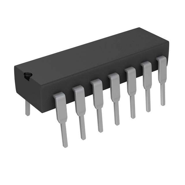
| 描述 | IC OPAMP GP 1MHZ 14DIP运算放大器 - 运放 Low Cost FET-Input Oper Amplifier |
| 产品分类 | Linear - Amplifiers - Instrumentation, OP Amps, Buffer Amps集成电路 - IC |
| 品牌 | Texas Instruments |
| 产品手册 | |
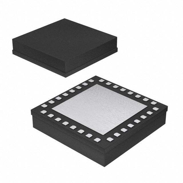
| 产品图片 |
|
| rohs | 符合RoHS无铅 / 符合限制有害物质指令(RoHS)规范要求 |
| 产品系列 | 放大器 IC,运算放大器 - 运放,Texas Instruments OPA4137PMicroAmplifier™ |
| 数据手册 | |
| 产品型号 | OPA4137P |
| 产品目录页面 | |
| 产品种类 | 运算放大器 - 运放 |
| 供应商器件封装 | 14-PDIP |
| 共模抑制比—最小值 | 74 dB |
| 关闭 | No Shutdown |
| 其它名称 | OPA4137PG4 |
| 包装 | 管件 |
| 单电源电压 | 4.5 V to 36 V |
| 压摆率 | 3.5 V/µs |
| 双重电源电压 | +/- 15 V |
| 商标 | Texas Instruments |
| 增益带宽生成 | 1 MHz |
| 增益带宽积 | 1MHz |
| 安装类型 | 通孔 |
| 安装风格 | Through Hole |
| 封装 | Tube |
| 封装/外壳 | 14-DIP(0.300",7.62mm) |
| 封装/箱体 | PDIP-14 |
| 工作温度 | -40°C ~ 85°C |
| 工作电源电压 | 4.5 V to 36 V, +/- 2.25 V to +/- 18 V |
| 工厂包装数量 | 25 |
| 技术 | BiFET |
| 放大器类型 | 通用 |
| 最大双重电源电压 | +/- 18 V |
| 最大工作温度 | + 85 C |
| 最小双重电源电压 | +/- 2.25 V |
| 最小工作温度 | - 40 C |
| 标准包装 | 25 |
| 电压-电源,单/双 (±) | 4.5 V ~ 36 V, ±2.25 V ~ 18 V |
| 电压-输入失调 | 1.5mV |
| 电流-电源 | 220µA |
| 电流-输入偏置 | 5pA |
| 电流-输出/通道 | 60mA |
| 电源电流 | 0.22 mA |
| 电路数 | 4 |
| 系列 | OPA4137 |
| 设计资源 | http://www.digikey.com/product-highlights/cn/zh/texas-instruments-webench-design-center/3176 |
| 转换速度 | 3.5 V/us |
| 输入偏压电流—最大 | 100 pA |
| 输入参考电压噪声 | 45 nV |
| 输入补偿电压 | 3 mV |
| 输出电流 | 60 mA |
| 输出类型 | - |
| 通道数量 | 4 Channel |


- 商务部:美国ITC正式对集成电路等产品启动337调查
- 曝三星4nm工艺存在良率问题 高通将骁龙8 Gen1或转产台积电
- 太阳诱电将投资9.5亿元在常州建新厂生产MLCC 预计2023年完工
- 英特尔发布欧洲新工厂建设计划 深化IDM 2.0 战略
- 台积电先进制程称霸业界 有大客户加持明年业绩稳了
- 达到5530亿美元!SIA预计今年全球半导体销售额将创下新高
- 英特尔拟将自动驾驶子公司Mobileye上市 估值或超500亿美元
- 三星加码芯片和SET,合并消费电子和移动部门,撤换高东真等 CEO
- 三星电子宣布重大人事变动 还合并消费电子和移动部门
- 海关总署:前11个月进口集成电路产品价值2.52万亿元 增长14.8%


PDF Datasheet 数据手册内容提取
® OPA137 OPA4137 OPA2137 OPA137 OPA4137 OPA4137 OPA2137 LOW COST FET-INPUT OPERATIONAL AMPLIFIERS Amplifier Series Micro ™ FEATURES DESCRIPTION l FET INPUT: I = 5pA OPA137 series FET-input operational amplifiers are designed B l LOW OFFSET VOLTAGE: 1.5mV for low cost and miniature applications. In addition to small size (SOT-23-5 and MSOP-8 packages), they provide low l WIDE SUPPLY RANGE: – 2.25V to – 18V input bias current (5pA), low quiescent currrent (220m A/ l LOW QUIESCENT CURRENT: 220m A/channel channel), and high open-loop gain (94dB). l EXCELLENT SPEED/POWER: 1MHz Either single (+4.5V to +36V) or dual (– 2.25 to – 18V) l INPUT TO POSITIVE SUPPLY supplies can be used. The input common-mode voltage range includes the positive supply—suitable for many single-supply l MicroSIZE PACKAGES: SOT-23-5, MSOP-8 applications. Single, dual, and quad versions have identical l SINGLE, DUAL, AND QUAD specifications for maximum design flexibility. OPA137 op amps are easy to use and free from phase inversion and overload problems found in some FET-input APPLICATIONS amplifiers. High performance, including linearity, is main- l STRAIN GAGE AMPLIFIER tained as the amplifiers swing to their specified limits. In addition, the combination of high slew rate (3.5V/m s) and l PHOTODETECTOR AMPLIFIER wide bandwidth (1MHz) provide fast settling time assuring l PRECISION INTEGRATOR good dynamic response. Dual and quad designs feature com- l BATTERY-POWERED INSTRUMENTS pletely independent circuitry for lowest crosstalk and freedom from interaction. l TEST EQUIPMENT The single (OPA137) packages are the tiny 5-lead SOT-23-5 l ACTIVE FILTERS surface mount, SO-8 surface mount, and 8-pin DIP. The dual (OPA2137) comes in the miniature MSOP-8 surface mount, SO-8 surface mount, and 8-pin DIP packages. The quad (OPA4137) packages are the SO-14 surface mount and the 14-pin DIP. All are specified from –40(cid:176) C to +85(cid:176) C and operate from –55(cid:176) C to +125(cid:176) C. A SPICE macromodel is available for design analysis. OPA137 NC 1 8 NC OPA4137 –In 2 7 V+ +In 3 6 Output Out A 1 14 Out D V– 4 5 NC OPA2137 –In A 2 13 –In D A D OPA137 +In A 3 12 +In D 8-Pin DIP, SO-8 Out A 1 8 V+ Out 1 5 V+ –In A 2 A 7 Out B V+ 4 11 V– +In B 5 10 +In C V– 2 +In A 3 B 6 –In B B C –In B 6 9 –In C +In 3 4 –In V– 4 5 +In B Out B 7 8 Out C SOT-23-5 8-Pin DIP, SO-8, MSOP-8 14-Pin DIP SO-14 International Airport Industrial Park • Mailing Address: PO Box 11400, Tucson, AZ 85734 • Street Address: 6730 S. Tucson Blvd., Tucson, AZ 85706 • Tel: (520) 746-1111 • Twx: 910-952-1111 Internet: http://www.burr-brown.com/ • FAXLine: (800) 548-6133 (US/Canada Only) • Cable: BBRCORP • Telex: 066-6491 • FAX: (520) 889-1510 • Immediate Product Info: (800) 548-6132 © 1998 Burr-Brown Corporation PDS-1438A Printed in U.S.A. August, 1998 SBOS089
– SPECIFICATIONS: V = 15V S At T = +25(cid:176)C, R = 10kW connected to ground, unless otherwise noted. A L Boldface limits apply over the specified temperature range, T = –40(cid:176)C to +85(cid:176)C. A OPA137N, U, P OPA137NA, UA, PA OPA2137E, U, P OPA2137EA, UA, PA OPA4137U, P OPA4137UA, PA PARAMETER CONDITION MIN TYP MAX MIN TYP MAX UNITS OFFSET VOLTAGE Input Offset Voltage V – 1.5 – 3 – 2.5 – 10 mV OS T = –40(cid:176)C to +85(cid:176)C – 2.5 – 7 – 3.5 – 15 mV A vs Temperature dV /dT T = –40(cid:176)C to +85(cid:176)C – 15 [ m V/(cid:176)C OS A vs Power Supply PSRR V = – 3V to – 18V – 90 – 250 [ [ m V/V S T = –40(cid:176)C to +85(cid:176)C – 250 [ m V/V A Channel Separation (dual, quad) dc 0.6 [ m V/V INPUT BIAS CURRENT V = 0V CM Input Bias Current I – 5 – 100 [ [ pA B vs Temperature See Typical Curve [ Input Offset Current I – 2 – 50 [ [ pA OS NOISE Input Voltage Noise, f = 0.1 to 10Hz 2 [ m Vp-p Input Voltage Noise Density, f = 1kHz e 45 [ nV/(cid:214) Hz n Current Noise Density, f = 1kHz i 1.2 [ fA/(cid:214) Hz n INPUT VOLTAGE RANGE Common-Mode Voltage Range V (V–) + 3 (V+) [ [ V CM Common-Mode Rejection Ratio CMRR V = –12V to 15V CM OPA137, OPA2137 76 84 70 [ dB OPA4137 74 84 70 [ dB T = –40(cid:176)C to +85(cid:176)C V = –12V to 15V A CM OPA137, OPA2137 72 70 dB OPA4137 70 70 dB INPUT IMPEDANCE Differential 1010 || 1 [ W || pF Common-Mode 1012 || 2 [ W || pF OPEN-LOOP GAIN Open-Loop Voltage Gain A V = –13.8V to 13.9V 86 94 [ [ dB OL O T = –40(cid:176)C to +85(cid:176)C V = –13.8V to 13.9V 86 [ dB A O FREQUENCY RESPONSE Gain-Bandwidth Product GBW 1 [ MHz Slew Rate SR G = 1 3.5 [ V/m s Settling Time, 0.1% G = 1, 10V Step, C = 100pF 8 [ m s L 0.01% G = 1, 10V Step, C = 100pF 10 [ m s L Overload Recovery Time V • G = V 1 [ m s IN S Total Harmonic Distortion + Noise THD+N G = 1, f = 1kHz, 3.5Vrms 0.05 [ % OUTPUT Voltage Output V (V–) + 1.2 (V+) – 1.1 [ [ V OUT T = –40(cid:176)C to +85(cid:176)C (V–) + 1.2 (V+) – 1.1 [ [ V A Short-Circuit Current I –25/+60 [ mA SC Capacitive Load Drive C 1000 [ pF LOAD POWER SUPPLY Specified Operating Range V – 15 [ V S Operating Voltage Range Dual Supplies – 2.25(1) – 18 [ [ V Single Supply +4.5 +36 [ [ V Quiescent Current I I = 0 – 220 – 270 [ [ m A Q O T = –40(cid:176)C to +85(cid:176)C I = 0 – 375 [ m A A O TEMPERATURE RANGE Specified Range –40 +85 [ [ (cid:176)C Operating Range –55 +125 [ [ (cid:176)C Storage Range –55 +125 [ [ (cid:176)C Thermal Resistance q JA SOT-23-5 Surface Mount 200 [ (cid:176)C/W MSOP-8 Surface Mount 150 [ (cid:176)C/W SO-8 Surface Mount 150 [ (cid:176)C/W 8-Pin DIP 100 [ (cid:176)C/W SO-14 Surface Mount 100 [ (cid:176)C/W 14-Pin DIP 80 [ (cid:176)C/W [ Specifications the same as OPA137N, U, P. NOTE: (1) At minimum power supply voltage inputs must be biased above ground in accordance with common-mode voltage range restrictions—see “Operating Voltage” discussion. ® OPA137, 2137, 4137 2
ABSOLUTE MAXIMUM RATINGS(1) ELECTROSTATIC Supply Voltage, V+ to V–.....................................................................36V DISCHARGE SENSITIVITY Input Voltage.......................................................(V–) –0.7V to (V+) +0.7V Input Current.......................................................................................2mA This integrated circuit can be damaged by ESD. Burr-Brown Output Short-Circuit(2)..............................................................Continuous Operating Temperature..................................................–55(cid:176)C to +125(cid:176)C recommends that all integrated circuits be handled with Storage Temperature......................................................–55(cid:176)C to +125(cid:176)C appropriate precautions. Failure to observe proper handling Junction Temperature....................................................................+150(cid:176)C and installation procedures can cause damage. Lead Temperature (soldering, 10s).................................................300(cid:176)C NOTE: (1) Stresses above these ratings may cause permanent damage. ESD damage can range from subtle performance degrada- Exposure to absolute maximum ratings for extended periods may affact device tion to complete device failure. Precision integrated circuits reliability. (2) Short circuit to ground, one amplifier per package. may be more susceptible to damage because very small parametric changes could cause the device not to meet its published specifications. PACKAGE/ORDERING INFORMATION PACKAGE SPECIFIED DRAWING TEMPERATURE PACKAGE ORDERING TRANSPORT PRODUCT PACKAGE NUMBER(1) RANGE MARKING NUMBER(2) MEDIA Single OPA137N 5-Lead SOT-23-5 Surface Mount 331 –40(cid:176)C to +85(cid:176)C E37(3) OPA137N/250 Tape and Reel " " " " " OPA137N/3K Tape and Reel OPA137NA 5-Lead SOT-23-5 Surface Mount 331 –40(cid:176)C to +85(cid:176)C E37(3) OPA137NA/250 Tape and Reel " " " " " OPA137NA/3K Tape and Reel OPA137U SO-8 Surface Mount 182 –40(cid:176)C to +85(cid:176)C OPA137U OPA137U Rails " " " " " OPA137U/2K5 Tape and Reel OPA137UA SO-8 Surface Mount 182 –40(cid:176)C to +85(cid:176)C OPA137UA OPA137UA Rails " " " " " OPA137UA/2K5 Tape and Reel OPA137P 8-Pin DIP 006 –40(cid:176)C to +85(cid:176)C OPA137P OPA137P Rails OPA137PA 8-Pin DIP 006 –40(cid:176)C to +85(cid:176)C OPA137PA OPA137PA Rails Dual OPA2137E MSOP-8 Surface Mount 337 –40(cid:176)C to +85(cid:176)C E37(3) OPA2137E/250 Tape and Reel " " " " " OPA2137E/2K5 Tape and Reel OPA2137EA MSOP-8 Surface Mount 337 –40(cid:176)C to +85(cid:176)C E37(3) OPA2137EA/250 Tape and Reel " " " " " OPA2137EA/2K5 Tape and Reel OPA2137U SO-8 Surface Mount 182 –40(cid:176)C to +85(cid:176)C OPA2137U OPA2137U Rails " " " " " OPA2137U/2K5 Tape and Reel OPA2137UA SO-8 Surface Mount 182 –40(cid:176)C to +85(cid:176)C OPA2137UA OPA2137UA Rails " " " " " OPA2137UA/2K5 Tape and Reel OPA2137P 8-Pin DIP 006 –40(cid:176)C to +85(cid:176)C OPA2137P OPA2137P Rails OPA2137PA 8-Pin DIP 006 –40(cid:176)C to +85(cid:176)C OPA2137PA OPA2137PA Rails Quad OPA4137U SO-14 Surface Mount 235 –40(cid:176)C to +85(cid:176)C OPA4137U OPA4137U Rails " " " " " OPA4137U/2K5 Tape and Reel OPA4137UA SO-14 Surface Mount 235 –40(cid:176)C to +85(cid:176)C OPA4137UA OPA4137UA Rails " " " " " OPA4137UA/2K5 Tape and Reel OPA4137P 14-Pin DIP 010 –40(cid:176)C to +85(cid:176)C OPA4137P OPA4137P Rails OPA4137PA 14-Pin DIP 010 –40(cid:176)C to +85(cid:176)C OPA4137PA OPA4137PA Rails NOTES: (1) For detailed drawing and dimension table, please see end of data sheet, or Appendix C of Burr-Brown IC Data Book. (2) Models with a slash (/) are available only in Tape and Reel in the quantities indicated (e.g., /2K5 indicates 2500 devices per reel). Ordering 3000 pieces of “OPA137NA/3K” will get a single 3000-piece Tape and Reel. For detailed Tape and Reel mechanical information, refer to Appendix B of Burr-Brown IC Data Book. (3) Grade information is marked on the reel. The information provided herein is believed to be reliable; however, BURR-BROWN assumes no responsibility for inaccuracies or omissions. BURR-BROWN assumes no responsibility for the use of this information, and all use of such information shall be entirely at the user’s own risk. Prices and specifications are subject to change without notice. No patent rights or licenses to any of the circuits described herein are implied or granted to any third party. BURR-BROWN does not authorize or warrant any BURR-BROWN product for use in life support devices and/or systems. ® 3 OPA137, 2137, 4137
TYPICAL PERFORMANCE CURVES At T = +25(cid:176)C, V = – 15V, R = 10kW , connected to ground, unless otherwise noted. A S L POWER SUPPLY AND COMMON-MODE REJECTION OPEN-LOOP GAIN/PHASE vs FREQUENCY vs FREQUENCY 100 100 80 0 G 80 +PSRR B) Gain (dB) 6400 –40°C f ––4950 ase Shift (°) R, CMRR (d 6400 CMRR 20 +85°C –135 Ph PSR –PSRR 20 0 +25°C –180 –20 0 1 10 100 1k 10k 100k 1M 10M 10 100 1k 10k 100k 1M Frequency (Hz) Frequency (Hz) INPUT VOLTAGE AND CURRENT NOISE SPECTRAL DENSITY vs FREQUENCY CHANNEL SEPARATION vs FREQUENCY 1k 1 140 120 Hz) Voltage Noise Hz) dB) (cid:214)Voltage Noise (nV/ 11000 Current Noise 110 (cid:214)Current Noise (fA/ hannel Separation ( 1086000 DGQu u=aa ld1 a ,m n adel laq csuhuaarden dnd eeclvhsia.cnens.el C A to D or B to C—other 40 combinations yield improved rejection. 1 0.1 20 0.1 1 10 100 1k 10k 100k 1M 100 1k 10k 100k 1M Frequency (Hz) Frequency (Hz) INPUT BIAS CURRENT INPUT BIAS CURRENT vs TEMPERATURE vs INPUT COMMON-MODE VOLTAGE 10k 1n Input bias current is a function of the voltage 1k between the V– supply A) A) and the inputs. Current (p 100 Current (p 100p Input Bias 110 Input Bias 10p 0.1 1p –75 –50 –25 0 25 50 75 100 125 –15 –10 –5 0 5 10 15 Temperature (°C) Common-Mode Voltage (V) ® OPA137, 2137, 4137 4
TYPICAL PERFORMANCE CURVES (CONT) At T = +25(cid:176)C, V = – 15V, R = 10kW , connected to ground, unless otherwise noted. A S L TOTAL HARMONIC DISTORTION + NOISE vs FREQUENCY A , CMRR, PSRR vs TEMPERATURE OL 1 95 V = –13.8V to +13.9V A O OL 90 G = 10 dB) R ( 85 CMRR %) SR +N ( 0.1 R, P 80 PSRR D R H M T C 75 G = 1 , OL A 70 V = 3.5Vrms O 0.01 65 100 1k 10k 100k –75 –50 –25 0 25 50 75 100 125 Frequency (Hz) Temperature (°C) QUIESCENT CURRENT and SHORT-CIRCUIT CURRENT QUIESCENT CURRENT and SHORT-CIRCUIT CURRENT vs TEMPERATURE vs SUPPLY VOLTAGE – 400 – 80 ±230 ±70 – 350 (IQ Per Amplifier) – 70 ±220 (IQ Per Amplifier) ±60 µQuiescent Current (A) ––––– 322110505000000 IQ +–IISSCC ––––– 6543200000 Short-Circuit Current (mA) Quiescent Current (µA) ±±±±221110980000 IQ –IS±CISC ±±±±54320000 Short-Circuit Current (mA) – 50 – 10 ±170 ±10 0 0 ±160 0 –75 –50 –25 0 25 50 75 100 125 0 ±5 ±10 ±15 ±20 Temperature (°C) Supply Voltage (V) MAXIMUM OUTPUT VOLTAGE vs FREQUENCY OUTPUT VOLTAGE SWING vs OUTPUT CURRENT 30 V = – 15V (V+) S Maximum output voltage 25 without visible dynamic (V+) –1 –55°C distortion. V) ge (Vp-p) 20 CL = 100pF e Swing ( ((VV++)) ––23 +125°C +25°C Output Volta 1150 CL = 200pF iWndituhcoeudt sdlieswto-rrtaioten utput Voltag ((VV––)) ++32 +125°C +25°C O 5 (V–) +1 V = – 5V –55°C S 0 (V–) 10k 100k 1M 0 ±2 ±4 ±6 ±8 ±10 Frequency (Hz) Output Current (mA) ® 5 OPA137, 2137, 4137
TYPICAL PERFORMANCE CURVES (CONT) At T = +25(cid:176)C, V = – 15V, R = 10kW , connected to ground, unless otherwise noted. A S L OFFSET VOLTAGE DRIFT OFFSET VOLTAGE PRODUCTION DISTRIBUTION PRODUCTION DISTRIBUTION 20 20 Typical production Typical production 18 distribution of 18 distribution of mplifiers (%) 11116420 pSqauincagkdlaesg ,i enddcul auuldnse,it dsa..n d mplifiers (%) 11116420 pSqauincagkdlaesg ,i enddcul auuldnse,it dsa..n d A A Percent of 864 Percent of 864 2 2 0 0 –10–9–8–7–6–5–4–3–2–1012345678910 048121620242832364044485256606468827680 Offset Voltage (mV) Offset Voltage Drift (µV/°C) SMALL-SIGNAL OVERSHOOT SETTLING TIME vs CLOSED-LOOP GAIN vs LOAD CAPACITANCE 100 60 10V Step 50 0.01% ettling Time (µs) 10 0.1% Overshoot (%) 432000 G = –1 S 10 G = +10 G = +1 1 0 1 10 100 10 100 1k 10k Closed-Loop Gain (V/V) Load Capacitance (pF) SMALL-SIGNAL STEP RESPONSE LARGE-SIGNAL STEP RESPONSE G = 1, CL = 50pF G = 1, CL = 50pF v di v V/ di m V/ 0 5 2 1m s/div 5m s/div ® OPA137, 2137, 4137 6
APPLICATIONS INFORMATION HIGH-SIDE CURRENT SENSING Many applications require the sensing of signals near the OPA137 series op amps are unity-gain stable and suitable positive supply. The common-mode input range of OPA137 for a wide range of general-purpose applications. Power op amps includes the positive rail, enabling them to be used supply pins should be bypassed with 10nF ceramic capaci- to sense power supply currents as shown in Figure 2. tors or larger. All circuitry is completely independent in dual and quad versions, assuring normal performance when one amplifier in a package is overdriven or short circuited. Many R 1 key parameters are guaranteed over the specified tempera- 0.1W ture range, –40(cid:176) C to +85(cid:176) C. V+ R 2 1kW Load OPERATING VOLTAGE OPA137 op amps can be operated on power supplies as low as – 2.25V. Performance remains excellent with power sup- OPA137 plies ranging from – 2.25V to – 18V (+4.5V to +36V single supply). Most parameters vary only slightly throughout this 20pF supply voltage range. Quiescent current and short-circuit R R current vs supply voltage are shown in Typical Performance V = 1 3 I O R L Curves. 2 Zetex Operation at very low supply voltage (V £ – 3V) requires Darlington S ZTX712 careful attention to ensure that the common-mode voltage OPA241 VO remains within the linear range, V = (V–)+3V to (V+). CM Ground-referred Inputs may need to be biased above ground in accordance output R with the common-mode voltage range restrictions for linear 3 10kW operation. INPUT VOLTAGE FIGURE 2. High-Side Current Monitor. The input common-mode voltage range of OPA137 series INPUT BIAS CURRENT op amps extends from (V–)+3V to the positive rail, V+. For normal operation, inputs should be limited to this range. The The input bias current is approximately 5pA at room tem- inputs may go beyond the power supplies without output perature and increases with temperature as shown in the phase-reversal. Many FET-input op amps (such as TL061 typical performance curve “Input Bias Current vs Tempera- types) exhibit phase-reversal of the output when the input ture.” common-mode range is exceeded. This can occur in voltage- Input Bias current also varies with common-mode voltage follower circuits, causing serious problems in control loop and power supply voltage. This variation is dependent on applications. the voltage between the negative power supply and the Input terminals are diode-clamped to the power supply rails common-mode input voltage. The effect is shown in the for ESD protection. If the input voltage can exceed the typical performance curve “Input Bias Current vs Common- negative supply by 500mV, input current should be limited Mode Voltage.” to 2mA (or less). If the input current is not adequately limited, you may see unpredicatable behavior in the other amplifiers in the package. This is easily accomplished with an input resistor as shown in Figure 1. Many input signals R F are inherently current-limited, therefore, a limiting resistor 1MW may not be required. 3.3pF V+ I l D OPA137 VO = – RF ID I OVERLOAD 2mA max Photodiode OPA137 V OUT BPW34 VIN C = 75pF ID is proportional to D light intensity (radiant power) Inputs are internally V– clamped to V+ and V– FIGURE 3. Photodetector Amplifier. FIGURE 1. Input Current Protection for Voltages Exceed- ing the Supply Voltage. ® 7 OPA137, 2137, 4137
SOT-23-5 MSOP-8 (Package Drawing #331) (Package Drawing #337) 0.075 0.027 (1.905) (0.686) 0.035(0.889) 0.10(2.54) 0.19(4.83) 0.041.016) 0.0375 ( 0.0375 (0.9525) (0.9525) 0.016 0.0256 (0.41) (0.65) Refer to end of data sheet or Appendix C of Burr-Brown Data Book for tolerances and detailed package drawing. For further information on solder pads for surface-mount devices consult Application Bulletin AB-132. FIGURE 4. Recommended SOT-23-5 and MSOP-8 Solder Footprints. ® OPA137, 2137, 4137 8
PACKAGE OPTION ADDENDUM www.ti.com 6-Feb-2020 PACKAGING INFORMATION Orderable Device Status Package Type Package Pins Package Eco Plan Lead/Ball Finish MSL Peak Temp Op Temp (°C) Device Marking Samples (1) Drawing Qty (2) (6) (3) (4/5) OPA137N/250 ACTIVE SOT-23 DBV 5 250 Green (RoHS NIPDAU Level-2-260C-1 YEAR -40 to 85 E37 & no Sb/Br) OPA137N/3K ACTIVE SOT-23 DBV 5 3000 Green (RoHS NIPDAU Level-2-260C-1 YEAR -40 to 85 E37 & no Sb/Br) OPA137N/3KE4 ACTIVE SOT-23 DBV 5 3000 Green (RoHS NIPDAU Level-2-260C-1 YEAR -40 to 85 E37 & no Sb/Br) OPA137NA/250 ACTIVE SOT-23 DBV 5 250 Green (RoHS NIPDAU Level-2-260C-1 YEAR -40 to 85 E37 & no Sb/Br) OPA137NA/250E4 ACTIVE SOT-23 DBV 5 250 Green (RoHS NIPDAU Level-2-260C-1 YEAR -40 to 85 E37 & no Sb/Br) OPA137NA/3K ACTIVE SOT-23 DBV 5 3000 Green (RoHS NIPDAU Level-2-260C-1 YEAR -40 to 85 E37 & no Sb/Br) OPA137U ACTIVE SOIC D 8 75 Green (RoHS NIPDAU Level-3-260C-168 HR -40 to 85 OPA & no Sb/Br) 137U OPA137UA ACTIVE SOIC D 8 75 Green (RoHS NIPDAU Level-3-260C-168 HR -40 to 85 OPA & no Sb/Br) 137U A OPA137UA/2K5 ACTIVE SOIC D 8 2500 Green (RoHS NIPDAU Level-3-260C-168 HR -40 to 85 OPA & no Sb/Br) 137U A OPA2137E/250 ACTIVE VSSOP DGK 8 250 Green (RoHS Call TI | NIPDAU Level-3-260C-168 HR -40 to 85 E37 & no Sb/Br) OPA2137E/2K5 ACTIVE VSSOP DGK 8 2500 Green (RoHS Call TI | NIPDAU Level-3-260C-168 HR -40 to 85 E37 & no Sb/Br) OPA2137E/2K5G4 ACTIVE VSSOP DGK 8 2500 Green (RoHS Call TI Level-3-260C-168 HR -40 to 85 E37 & no Sb/Br) OPA2137EA/250 ACTIVE VSSOP DGK 8 250 Green (RoHS Call TI | NIPDAU Level-3-260C-168 HR E37 & no Sb/Br) OPA2137EA/250G4 ACTIVE VSSOP DGK 8 250 Green (RoHS Call TI Level-3-260C-168 HR E37 & no Sb/Br) OPA2137EA/2K5 ACTIVE VSSOP DGK 8 2500 Green (RoHS Call TI | NIPDAU Level-3-260C-168 HR E37 & no Sb/Br) OPA2137P ACTIVE PDIP P 8 50 Green (RoHS NIPDAU N / A for Pkg Type OPA2137P & no Sb/Br) Addendum-Page 1
PACKAGE OPTION ADDENDUM www.ti.com 6-Feb-2020 Orderable Device Status Package Type Package Pins Package Eco Plan Lead/Ball Finish MSL Peak Temp Op Temp (°C) Device Marking Samples (1) Drawing Qty (2) (6) (3) (4/5) OPA2137PA ACTIVE PDIP P 8 50 Green (RoHS NIPDAU N / A for Pkg Type OPA2137P & no Sb/Br) A OPA2137U ACTIVE SOIC D 8 75 Green (RoHS NIPDAU Level-3-260C-168 HR OPA & no Sb/Br) 2137U OPA2137U/2K5 ACTIVE SOIC D 8 2500 Green (RoHS NIPDAU Level-3-260C-168 HR OPA & no Sb/Br) 2137U OPA2137UA ACTIVE SOIC D 8 75 Green (RoHS NIPDAU Level-3-260C-168 HR -40 to 85 OPA & no Sb/Br) 2137U A OPA2137UA/2K5 ACTIVE SOIC D 8 2500 Green (RoHS NIPDAU Level-3-260C-168 HR -40 to 85 OPA & no Sb/Br) 2137U A OPA4137P ACTIVE PDIP N 14 25 Green (RoHS NIPDAU N / A for Pkg Type OPA4137P & no Sb/Br) OPA4137PA ACTIVE PDIP N 14 25 Green (RoHS NIPDAU N / A for Pkg Type OPA4137P & no Sb/Br) A OPA4137PAG4 ACTIVE PDIP N 14 25 Green (RoHS NIPDAU N / A for Pkg Type OPA4137P & no Sb/Br) A OPA4137U ACTIVE SOIC D 14 50 Green (RoHS NIPDAU Level-3-260C-168 HR -40 to 85 OPA4137U & no Sb/Br) OPA4137U/2K5 ACTIVE SOIC D 14 2500 Green (RoHS NIPDAU Level-3-260C-168 HR -40 to 85 OPA4137U & no Sb/Br) OPA4137UA ACTIVE SOIC D 14 50 Green (RoHS NIPDAU Level-3-260C-168 HR -40 to 85 OPA4137U & no Sb/Br) A OPA4137UA/2K5 ACTIVE SOIC D 14 2500 Green (RoHS NIPDAU Level-3-260C-168 HR -40 to 85 OPA4137U & no Sb/Br) A OPA4137UAE4 ACTIVE SOIC D 14 50 Green (RoHS NIPDAU Level-3-260C-168 HR -40 to 85 OPA4137U & no Sb/Br) A OPA4137UAG4 ACTIVE SOIC D 14 50 Green (RoHS NIPDAU Level-3-260C-168 HR -40 to 85 OPA4137U & no Sb/Br) A (1) The marketing status values are defined as follows: ACTIVE: Product device recommended for new designs. LIFEBUY: TI has announced that the device will be discontinued, and a lifetime-buy period is in effect. NRND: Not recommended for new designs. Device is in production to support existing customers, but TI does not recommend using this part in a new design. PREVIEW: Device has been announced but is not in production. Samples may or may not be available. OBSOLETE: TI has discontinued the production of the device. Addendum-Page 2
PACKAGE OPTION ADDENDUM www.ti.com 6-Feb-2020 (2) RoHS: TI defines "RoHS" to mean semiconductor products that are compliant with the current EU RoHS requirements for all 10 RoHS substances, including the requirement that RoHS substance do not exceed 0.1% by weight in homogeneous materials. Where designed to be soldered at high temperatures, "RoHS" products are suitable for use in specified lead-free processes. TI may reference these types of products as "Pb-Free". RoHS Exempt: TI defines "RoHS Exempt" to mean products that contain lead but are compliant with EU RoHS pursuant to a specific EU RoHS exemption. Green: TI defines "Green" to mean the content of Chlorine (Cl) and Bromine (Br) based flame retardants meet JS709B low halogen requirements of <=1000ppm threshold. Antimony trioxide based flame retardants must also meet the <=1000ppm threshold requirement. (3) MSL, Peak Temp. - The Moisture Sensitivity Level rating according to the JEDEC industry standard classifications, and peak solder temperature. (4) There may be additional marking, which relates to the logo, the lot trace code information, or the environmental category on the device. (5) Multiple Device Markings will be inside parentheses. Only one Device Marking contained in parentheses and separated by a "~" will appear on a device. If a line is indented then it is a continuation of the previous line and the two combined represent the entire Device Marking for that device. (6) Lead/Ball Finish - Orderable Devices may have multiple material finish options. Finish options are separated by a vertical ruled line. Lead/Ball Finish values may wrap to two lines if the finish value exceeds the maximum column width. Important Information and Disclaimer:The information provided on this page represents TI's knowledge and belief as of the date that it is provided. TI bases its knowledge and belief on information provided by third parties, and makes no representation or warranty as to the accuracy of such information. Efforts are underway to better integrate information from third parties. TI has taken and continues to take reasonable steps to provide representative and accurate information but may not have conducted destructive testing or chemical analysis on incoming materials and chemicals. TI and TI suppliers consider certain information to be proprietary, and thus CAS numbers and other limited information may not be available for release. In no event shall TI's liability arising out of such information exceed the total purchase price of the TI part(s) at issue in this document sold by TI to Customer on an annual basis. Addendum-Page 3
PACKAGE MATERIALS INFORMATION www.ti.com 9-Aug-2017 TAPE AND REEL INFORMATION *Alldimensionsarenominal Device Package Package Pins SPQ Reel Reel A0 B0 K0 P1 W Pin1 Type Drawing Diameter Width (mm) (mm) (mm) (mm) (mm) Quadrant (mm) W1(mm) OPA137N/250 SOT-23 DBV 5 250 178.0 8.4 3.3 3.2 1.4 4.0 8.0 Q3 OPA137N/3K SOT-23 DBV 5 3000 178.0 8.4 3.3 3.2 1.4 4.0 8.0 Q3 OPA137NA/250 SOT-23 DBV 5 250 178.0 8.4 3.23 3.17 1.37 4.0 8.0 Q3 OPA137NA/3K SOT-23 DBV 5 3000 178.0 8.4 3.3 3.2 1.4 4.0 8.0 Q3 OPA137UA/2K5 SOIC D 8 2500 330.0 12.4 6.4 5.2 2.1 8.0 12.0 Q1 OPA2137E/250 VSSOP DGK 8 250 180.0 12.4 5.3 3.4 1.4 8.0 12.0 Q1 OPA2137E/2K5 VSSOP DGK 8 2500 330.0 12.4 5.3 3.4 1.4 8.0 12.0 Q1 OPA2137EA/250 VSSOP DGK 8 250 180.0 12.4 5.3 3.4 1.4 8.0 12.0 Q1 OPA2137EA/2K5 VSSOP DGK 8 2500 330.0 12.4 5.3 3.4 1.4 8.0 12.0 Q1 OPA2137U/2K5 SOIC D 8 2500 330.0 12.4 6.4 5.2 2.1 8.0 12.0 Q1 OPA2137UA/2K5 SOIC D 8 2500 330.0 12.4 6.4 5.2 2.1 8.0 12.0 Q1 OPA4137U/2K5 SOIC D 14 2500 330.0 16.4 6.5 9.0 2.1 8.0 16.0 Q1 OPA4137UA/2K5 SOIC D 14 2500 330.0 16.4 6.5 9.0 2.1 8.0 16.0 Q1 PackMaterials-Page1
PACKAGE MATERIALS INFORMATION www.ti.com 9-Aug-2017 *Alldimensionsarenominal Device PackageType PackageDrawing Pins SPQ Length(mm) Width(mm) Height(mm) OPA137N/250 SOT-23 DBV 5 250 565.0 140.0 75.0 OPA137N/3K SOT-23 DBV 5 3000 565.0 140.0 75.0 OPA137NA/250 SOT-23 DBV 5 250 565.0 140.0 75.0 OPA137NA/3K SOT-23 DBV 5 3000 565.0 140.0 75.0 OPA137UA/2K5 SOIC D 8 2500 367.0 367.0 35.0 OPA2137E/250 VSSOP DGK 8 250 210.0 185.0 35.0 OPA2137E/2K5 VSSOP DGK 8 2500 367.0 367.0 35.0 OPA2137EA/250 VSSOP DGK 8 250 210.0 185.0 35.0 OPA2137EA/2K5 VSSOP DGK 8 2500 367.0 367.0 35.0 OPA2137U/2K5 SOIC D 8 2500 367.0 367.0 35.0 OPA2137UA/2K5 SOIC D 8 2500 367.0 367.0 35.0 OPA4137U/2K5 SOIC D 14 2500 367.0 367.0 38.0 OPA4137UA/2K5 SOIC D 14 2500 367.0 367.0 38.0 PackMaterials-Page2
IMPORTANTNOTICEANDDISCLAIMER TI PROVIDES TECHNICAL AND RELIABILITY DATA (INCLUDING DATASHEETS), DESIGN RESOURCES (INCLUDING REFERENCE DESIGNS), APPLICATION OR OTHER DESIGN ADVICE, WEB TOOLS, SAFETY INFORMATION, AND OTHER RESOURCES “AS IS” AND WITH ALL FAULTS, AND DISCLAIMS ALL WARRANTIES, EXPRESS AND IMPLIED, INCLUDING WITHOUT LIMITATION ANY IMPLIED WARRANTIES OF MERCHANTABILITY, FITNESS FOR A PARTICULAR PURPOSE OR NON-INFRINGEMENT OF THIRD PARTY INTELLECTUAL PROPERTY RIGHTS. These resources are intended for skilled developers designing with TI products. You are solely responsible for (1) selecting the appropriate TI products for your application, (2) designing, validating and testing your application, and (3) ensuring your application meets applicable standards, and any other safety, security, or other requirements. These resources are subject to change without notice. TI grants you permission to use these resources only for development of an application that uses the TI products described in the resource. Other reproduction and display of these resources is prohibited. No license is granted to any other TI intellectual property right or to any third party intellectual property right. TI disclaims responsibility for, and you will fully indemnify TI and its representatives against, any claims, damages, costs, losses, and liabilities arising out of your use of these resources. TI’s products are provided subject to TI’s Terms of Sale (www.ti.com/legal/termsofsale.html) or other applicable terms available either on ti.com or provided in conjunction with such TI products. TI’s provision of these resources does not expand or otherwise alter TI’s applicable warranties or warranty disclaimers for TI products. Mailing Address: Texas Instruments, Post Office Box 655303, Dallas, Texas 75265 Copyright © 2020, Texas Instruments Incorporated