ICGOO在线商城 > 集成电路(IC) > 线性 - 放大器 - 仪表,运算放大器,缓冲器放大器 > OPA333AIDR

 Datasheet下载
- 型号: OPA333AIDR
- 制造商: Texas Instruments
- 库位|库存: xxxx|xxxx
- 要求:
| 数量阶梯 | 香港交货 | 国内含税 |
| +xxxx | $xxxx | ¥xxxx |
查看当月历史价格
查看今年历史价格
OPA333AIDR产品简介:
ICGOO电子元器件商城为您提供OPA333AIDR由Texas Instruments设计生产,在icgoo商城现货销售,并且可以通过原厂、代理商等渠道进行代购。 OPA333AIDR价格参考¥6.94-¥15.63。Texas InstrumentsOPA333AIDR封装/规格:线性 - 放大器 - 仪表,运算放大器,缓冲器放大器, 零漂移 放大器 1 电路 满摆幅 8-SOIC。您可以下载OPA333AIDR参考资料、Datasheet数据手册功能说明书,资料中有OPA333AIDR 详细功能的应用电路图电压和使用方法及教程。
Texas Instruments(德州仪器)的OPA333AIDR是一款低功耗、零漂移、轨到轨输入输出运算放大器,适用于多种精密信号处理应用场景。以下是一些具体的应用场景:

1. 传感器信号调理:OPA333AIDR具有极低的偏置电流和输入失调电压,非常适合用于高阻抗传感器信号的放大和调理。例如,在温度传感器、压力传感器或光电二极管等应用中,它可以提供高精度的信号放大,确保测量结果的准确性。

2. 医疗设备:在医疗设备中,如心电图(ECG)、脑电图(EEG)和血氧饱和度监测仪等,OPA333AIDR可以用于放大微弱的生物电信号。其低噪声和高共模抑制比(CMRR)特性,使得它能够在复杂电磁环境中保持稳定的性能。

3. 工业自动化:在工业控制系统中,OPA333AIDR可用于信号调理、反馈控制和数据采集。例如,在可编程逻辑控制器(PLC)中,它可以作为模拟输入模块的一部分,对传感器信号进行精确放大和转换,确保系统的稳定性和可靠性。

4. 便携式设备:由于其低功耗特性,OPA333AIDR非常适合用于电池供电的便携式设备,如手持式测量仪器、无线传感器节点等。它可以在不影响性能的前提下,延长电池寿命,提升用户体验。

5. 音频处理:在音频设备中,OPA333AIDR可以用于前置放大器或线路驱动器,提供高质量的音频信号放大。其低失真和低噪声特性,能够确保音频信号的纯净和清晰。

6. 电源管理:在电源管理系统中,OPA333AIDR可以用作误差放大器或电压基准缓冲器,帮助实现精确的电压调节和监控。其轨到轨输入输出特性,使其能够在宽电压范围内正常工作,适应不同的电源设计需求。

综上所述,OPA333AIDR凭借其低功耗、零漂移和高精度的特点,广泛应用于各种需要精密信号处理的场合,特别是在对噪声敏感和要求高稳定性的系统中表现出色。
| 参数 | 数值 |
| -3db带宽 | - |
| 产品目录 | 集成电路 (IC) |
| 描述 | IC OPAMP CHOPPER 350KHZ 8SOIC |
| 产品分类 | Linear - Amplifiers - Instrumentation, OP Amps, Buffer Amps |
| 品牌 | Texas Instruments |
| 数据手册 | |
| 产品图片 |
|
| 产品型号 | OPA333AIDR |
| rohs | 无铅 / 符合限制有害物质指令(RoHS)规范要求 |
| 产品系列 | - |
| 供应商器件封装 | 8-SOIC |
| 制造商产品页 | http://www.ti.com/general/docs/suppproductinfo.tsp?distId=10&orderablePartNumber=OPA333AIDR |
| 包装 | 带卷 (TR) |
| 压摆率 | 0.16 V/µs |
| 增益带宽积 | 350kHz |
| 安装类型 | 表面贴装 |
| 封装/外壳 | 8-SOIC(0.154",3.90mm 宽) |
| 工作温度 | -40°C ~ 125°C |
| 放大器类型 | 零漂移 |
| 标准包装 | 2,500 |
| 电压-电源,单/双 (±) | 1.8 V ~ 5.5 V, ±0.9 V ~ 2.75 V |
| 电压-输入失调 | 2µV |
| 电流-电源 | 17µA |
| 电流-输入偏置 | 70pA |
| 电流-输出/通道 | 5mA |
| 电路数 | 1 |
| 设计资源 | http://www.digikey.com/product-highlights/cn/zh/texas-instruments-webench-design-center/3176 |
| 输出类型 | 满摆幅 |


- 商务部:美国ITC正式对集成电路等产品启动337调查
- 曝三星4nm工艺存在良率问题 高通将骁龙8 Gen1或转产台积电
- 太阳诱电将投资9.5亿元在常州建新厂生产MLCC 预计2023年完工
- 英特尔发布欧洲新工厂建设计划 深化IDM 2.0 战略
- 台积电先进制程称霸业界 有大客户加持明年业绩稳了
- 达到5530亿美元!SIA预计今年全球半导体销售额将创下新高
- 英特尔拟将自动驾驶子公司Mobileye上市 估值或超500亿美元
- 三星加码芯片和SET,合并消费电子和移动部门,撤换高东真等 CEO
- 三星电子宣布重大人事变动 还合并消费电子和移动部门
- 海关总署:前11个月进口集成电路产品价值2.52万亿元 增长14.8%


PDF Datasheet 数据手册内容提取
Product Sample & Technical Tools & Support & Reference Folder Buy Documents Software Community Design OPA333,OPA2333 SBOS351E–MARCH2006–REVISEDDECEMBER2015 OPAx333 1.8-V, microPower, CMOS Operational Amplifiers, Zero-Drift Series 1 Features 3 Description • LowOffsetVoltage:10 μV(Maximum) The OPAx333 series of CMOS operational amplifiers 1 use a proprietary auto-calibration technique to • ZeroDrift:0.05 μV/°C(Maximum) simultaneously provide very low offset voltage • 0.01-Hzto10-HzNoise:1.1μVPP (10 μV, maximum) and near-zero drift over time and • QuiescentCurrent:17μA temperature. These miniature, high-precision, low quiescent current amplifiers offer high-impedance • Single-SupplyOperation inputs that have a common-mode range 100 mV • SupplyVoltage:1.8Vto5.5V beyond the rails, and rail-to-rail output that swings • Rail-to-RailInput/Output within 50 mV of the rails. Single or dual supplies as low as 1.8 V (±0.9 V) and up to 5.5 V (±2.75 V) can • microSizePackages:SC70andSOT23 be used. These devices are optimized for low- voltage,single-supplyoperation. 2 Applications The OPAx333 family offers excellent CMRR without • Transducers the crossover associated with traditional • TemperatureMeasurements complementary input stages. This design results in • ElectronicScales superior performance for driving analog-to-digital converters (ADCs) without degradation of differential • MedicalInstrumentation linearity. • Battery-PoweredInstruments The OPA333 (single version) is available in the 5-pin • HandheldTestEquipment SOT-23, SOT, and 8-pin SOIC packages, while the OPA2333 (dual version) is available in the 8-pin VSON, SOIC, and VSSOP packages. All versions are specifiedforoperationfrom –40°Cto125°C. DeviceInformation(1) PARTNUMBER PACKAGE BODYSIZE(NOM) SOT-23(5) 2.90mm×1.60mm OPA333 SOT(5) 2.00mmx1.25mm SOIC(8) 4.90mm×3.90mm VSON(8) 3.00mm×3.00mm OPA2333 SOIC(8) 4.90mm×3.90mm VSSOP(8) 3.00mm×3.00mm (1) For all available packages, see the orderable addendum at theendofthedatasheet. 0.1-Hzto10-HzNoise OPAx333PinoutDiagrams OPA333 OPA333 OUT 1 5 V+ +IN 1 5 V+ V- 2 V- 2 V/div +IN 3 4 -IN -IN 3 4 OUT n 0 50 SOT23-5 SC70-5 OPA2333 OUTA 1 8 V+ Exposed -INA 2 Thermal 7 OUTB 1 s/div Die Pad +INA 3 on 6 -IN B Underside V- 4 5 +IN B DFN-8 (SON-8) 1 An IMPORTANT NOTICE at the end of this data sheet addresses availability, warranty, changes, use in safety-critical applications, intellectualpropertymattersandotherimportantdisclaimers.PRODUCTIONDATA.
OPA333,OPA2333 SBOS351E–MARCH2006–REVISEDDECEMBER2015 www.ti.com Table of Contents 1 Features.................................................................. 1 8 ApplicationandImplementation........................ 15 2 Applications........................................................... 1 8.1 ApplicationInformation............................................15 3 Description............................................................. 1 8.2 TypicalApplications ...............................................15 4 RevisionHistory..................................................... 2 8.3 SystemExamples...................................................20 5 PinConfigurationandFunctions......................... 3 9 PowerSupplyRecommendations...................... 22 6 Specifications......................................................... 5 10 Layout................................................................... 23 6.1 AbsoluteMaximumRatings......................................5 10.1 LayoutGuidelines.................................................23 6.2 ESDRatings..............................................................5 10.2 LayoutExample....................................................23 6.3 RecommendedOperatingConditions.......................5 11 DeviceandDocumentationSupport................. 24 6.4 ThermalInformation:OPA333..................................6 11.1 DeviceSupport......................................................24 6.5 ThermalInformation:OPA2333................................6 11.2 DocumentationSupport........................................24 6.6 ElectricalCharacteristics...........................................7 11.3 RelatedLinks........................................................24 6.7 TypicalCharacteristics..............................................8 11.4 CommunityResources..........................................24 7 DetailedDescription............................................ 12 11.5 Trademarks...........................................................24 7.1 Overview.................................................................12 11.6 ElectrostaticDischargeCaution............................24 7.2 FunctionalBlockDiagram.......................................12 11.7 Glossary................................................................25 7.3 FeatureDescription.................................................12 12 Mechanical,Packaging,andOrderable Information........................................................... 25 7.4 DeviceFunctionalModes........................................14 4 Revision History NOTE:Pagenumbersforpreviousrevisionsmaydifferfrompagenumbersinthecurrentversion. ChangesfromRevisionD(November2013)toRevisionE Page • AddedPinConfigurationandFunctionssection,ESDRatingsandThermalInformationtables,FeatureDescription section,DeviceFunctionalModes,ApplicationandImplementationsection,PowerSupplyRecommendations section,Layoutsection,DeviceandDocumentationSupportsection,andMechanical,Packaging,andOrderable Informationsection ................................................................................................................................................................ 1 ChangesfromRevisionC(May2007)toRevisionD Page • Changeddatasheetformattomostcurrentstandardlookandfeel...................................................................................... 1 • AddedOPA2333DFN-8pinouttofrontpage......................................................................................................................... 1 • Changed2ndsignalinputterminalsparameterintheAbsoluteMaximumRatingsfrom"voltage"to"current"(typo)..........5 • AddedTable1........................................................................................................................................................................ 8 2 SubmitDocumentationFeedback Copyright©2006–2015,TexasInstrumentsIncorporated ProductFolderLinks:OPA333 OPA2333
OPA333,OPA2333 www.ti.com SBOS351E–MARCH2006–REVISEDDECEMBER2015 5 Pin Configuration and Functions OPA333DBVPackage 5-PinSOT OPA333DCKPackage TopView 5-PinSC70 TopView OUT 1 5 V+ +IN 1 5 V+ V- 2 V- 2 +IN 3 4 -IN -IN 3 4 OUT OPA333DPackage 8-PinSOIC TopView NC(1) 1 8 NC(1) -IN 2 7 V+ +IN 3 6 OUT V- 4 5 NC(1) PinFunctions:OPA333 PIN I/O DESCRIPTION NAME SOIC SOT SC70 +IN 3 3 1 I Noninvertinginput –IN 2 4 3 I Invertinginput NC 1,5,8 — — — Nointernalconnection(canbeleftfloating) OUT 6 1 4 O Output V+ 7 5 5 — Positive(highest)powersupply V– 4 2 2 — Negative(lowest)powersupply Copyright©2006–2015,TexasInstrumentsIncorporated SubmitDocumentationFeedback 3 ProductFolderLinks:OPA333 OPA2333
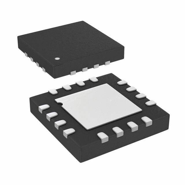
OPA333,OPA2333 SBOS351E–MARCH2006–REVISEDDECEMBER2015 www.ti.com OPA2333DRBPackage OPA2333DorDGKPackage 8-PinVSONWithExposedThermalPad 8-PinSOICorVSSOP TopView TopView OUT A 1 8 V+ OUT A 1 8 V+ A Exposed -IN A 2 7 OUT B -IN A 2 Thermal 7 OUT B Die Pad +IN A 3 B 6 -IN B +IN A 3 on 6 -IN B Underside(2) V- 4 5 +IN B V- 4 5 +IN B PinFunctions:OPA2333 PIN I/O DESCRIPTION NAME VSON SOIC,VSSOP +IN — — I Noninvertinginput +INA 3 3 I Noninvertinginput,channelA +INB 5 5 I Noninvertinginput,channelB –IN — — I Invertinginput –INA 2 2 I Invertinginput,channelA –INB 6 6 I Invertinginput,channelB OUT — — O Output OUTA 1 1 O Output,channelA OUTB 7 7 O Output,channelB V+ 8 8 — Positive(highest)powersupply V– 4 4 — Negative(lowest)powersupply 4 SubmitDocumentationFeedback Copyright©2006–2015,TexasInstrumentsIncorporated ProductFolderLinks:OPA333 OPA2333
OPA333,OPA2333 www.ti.com SBOS351E–MARCH2006–REVISEDDECEMBER2015 6 Specifications 6.1 Absolute Maximum Ratings See (1) MIN MAX UNIT Supply 7 Voltage V Signalinputterminals(2) –0.3 (V+)+0.3 Signalinputterminals(2) –1 1 Current mA Outputshort-circuit(3) Continuous Operatingjunctiontemperature,T 150 J Operatingtemperature,T –40 150 °C A Storagetemperature,T –65 150 stg (1) StressesbeyondthoselistedunderAbsoluteMaximumRatingsmaycausepermanentdamagetothedevice.Thesearestressratings only,whichdonotimplyfunctionaloperationofthedeviceattheseoranyotherconditionsbeyondthoseindicatedunderRecommended OperatingConditions.Exposuretoabsolute-maximum-ratedconditionsforextendedperiodsmayaffectdevicereliability. (2) Inputterminalsarediode-clampedtothepower-supplyrails.Inputsignalsthatcanswingmorethan0.3Vbeyondthesupplyrailsshould becurrentlimitedto10mAorless. (3) Short-circuittoground,oneamplifierperpackage. 6.2 ESD Ratings VALUE UNIT Electrostatic Humanbodymodel(HBM),perANSI/ESDA/JEDECJS-001(1) ±4000 V V (ESD) discharge Charged-devicemodel(CDM),perJEDECspecificationJESD22-C101(2) ±1000 (1) JEDECdocumentJEP155statesthat500-VHBMallowssafemanufacturingwithastandardESDcontrolprocess. (2) JEDECdocumentJEP157statesthat250-VCDMallowssafemanufacturingwithastandardESDcontrolprocess. 6.3 Recommended Operating Conditions overoperatingfree-airtemperaturerange(unlessotherwisenoted) MIN MAX UNIT Supplyvoltage,V 1.8 5.5 V S Specifiedtemperature –40 125 °C Copyright©2006–2015,TexasInstrumentsIncorporated SubmitDocumentationFeedback 5 ProductFolderLinks:OPA333 OPA2333
OPA333,OPA2333 SBOS351E–MARCH2006–REVISEDDECEMBER2015 www.ti.com 6.4 Thermal Information: OPA333 OPA333 THERMALMETRIC(1) D(SOIC) DBV(SOT) DCK(SC70) UNIT 8PINS 5PINS 5PINS R Junction-to-ambientthermalresistance 140.1 220.8 298.4 °C/W θJA R Junction-to-case(top)thermalresistance 89.8 97.5 65.4 °C/W θJC(top) R Junction-to-boardthermalresistance 80.6 61.7 97.1 °C/W θJB ψ Junction-to-topcharacterizationparameter 28.7 7.6 0.8 °C/W JT ψ Junction-to-boardcharacterizationparameter 80.1 61.1 95.5 °C/W JB R Junction-to-case(bottom)thermalresistance — — — °C/W θJC(bot) (1) Formoreinformationabouttraditionalandnewthermalmetrics,seetheSemiconductorandICPackageThermalMetricsapplication report,SPRA953. 6.5 Thermal Information: OPA2333 OPA2333 THERMALMETRIC(1) D(SOIC) DGK(VSSOP) DRB(VSON) UNIT 8PINS 8PINS 8PINS R Junction-to-ambientthermalresistance 124.0 180.3 46.7 °C/W θJA R Junction-to-case(top)thermalresistance 73.7 48.1 26.3 °C/W θJC(top) R Junction-to-boardthermalresistance 64.4 100.9 22.2 °C/W θJB ψ Junction-to-topcharacterizationparameter 18.0 2.4 1.6 °C/W JT ψ Junction-to-boardcharacterizationparameter 63.9 99.3 22.3 °C/W JB R Junction-to-case(bottom)thermalresistance — — 10.3 °C/W θJC(bot) (1) Formoreinformationabouttraditionalandnewthermalmetrics,seetheSemiconductorandICPackageThermalMetricsapplication report,SPRA953. 6 SubmitDocumentationFeedback Copyright©2006–2015,TexasInstrumentsIncorporated ProductFolderLinks:OPA333 OPA2333
OPA333,OPA2333 www.ti.com SBOS351E–MARCH2006–REVISEDDECEMBER2015 6.6 Electrical Characteristics AtT =25°C,R =10kΩconnectedtoV /2,V =V /2,andV =V /2,unlessotherwisenoted. A L S CM S OUT S PARAMETER TESTCONDITIONS MIN TYP MAX UNIT OFFSETVOLTAGE VOS Inputoffsetvoltage VS=5V 2 10 μV dVOS/dT Inputoffsetvoltagedrift TA=–40°Cto125°C 0.02 0.05 μV/°C PSRR Power-supplyrejectionratio VS=1.8Vto5.5V,TA=–40°Cto125°C 1 5 μV/V Long-termstability(1) Seenote(1) µV Channelseparation,dc 0.1 μV/V INPUTBIASCURRENT TA=25°C ±70 ±200 IB Inputbiascurrent TA=–40°Cto125°C ±150 pA IOS Inputoffsetcurrent ±140 ±400 NOISE f=0.01Hzto1Hz 0.3 Inputvoltagenoise μVPP f=0.1Hzto10Hz 1.1 in Inputcurrentnoise f=10Hz 100 fA/√Hz INPUTVOLTAGE VCM Common-modevoltagerange (V–)–0.1 (V+)+0.1 V CMRR Common-moderejectionratio (V–)–0.1V<VCM<(V+)+0.1V, 106 130 dB TA=–40°Cto125°C INPUTCAPACITANCE Differential 2 pF Common-mode 4 pF OPEN-LOOPGAIN AOL Open-loopvoltagegain (RVL–=)+1010k0Ω,mTVA<=V–4O0<°C(Vt+o)1–251°0C0mV, 106 130 dB FREQUENCYRESPONSE GBW Gain-bandwidthproduct CL=100pF 350 kHz SR Slewrate G=+1 0.16 V/μs OUTPUT RL=10kΩ 30 50 Voltageoutputswingfromrail mV RL=10kΩ,TA=–40°Cto125°C 70 ISC Short-circuitcurrent ±5 mA CL Capacitiveloaddrive SeeTypicalCharacteristics Open-loopoutputimpedance f=350kHz,IO=0A 2 kΩ POWERSUPPLY VS Specifiedvoltagerange 1.8 5.5 V IO=0A 17 25 IQ Quiescentcurrentperamplifier μA TA=–40°Cto125°C 28 Turn-ontime VS=+5V 100 μs TEMPERATURE Specifiedrange –40 125 °C TA Operatingrange –40 150 °C Tstg Storagerange –65 150 °C (1) 300-hourlifetestat150°Cdemonstratedrandomlydistributedvariationofapproximately1μV. Copyright©2006–2015,TexasInstrumentsIncorporated SubmitDocumentationFeedback 7 ProductFolderLinks:OPA333 OPA2333
OPA333,OPA2333 SBOS351E–MARCH2006–REVISEDDECEMBER2015 www.ti.com 6.7 Typical Characteristics Table1.ListofTypicalCharacteristics TITLE FIGURE OffsetVoltageProductionDistribution Figure1 OffsetVoltageDriftProductionDistribution Figure2 Open-LoopGainvsFrequency Figure3 Common-ModeRejectionRatiovsFrequency Figure4 Power-SupplyRejectionRatiovsFrequency Figure5 OutputVoltageSwingvsOutputCurrent Figure6 InputBiasCurrentvsCommon-ModeVoltage Figure7 InputBiasCurrentvsTemperature Figure8 QuiescentCurrentvsTemperature Figure9 Large-SignalStepResponse Figure10 Small-SignalStepResponse Figure11 PositiveOvervoltageRecovery Figure12 NegativeOvervoltageRecovery Figure13 SettlingTimevsClosed-LoopGain Figure14 Small-SignalOvershootvsLoadCapacitance Figure15 0.1-Hzto10-HzNoise Figure16 CurrentandVoltageNoiseSpectralDensityvsFrequency Figure17 AtT =25°C,V =5V,andC =0pF,unlessotherwisenoted. A S L n n o atio ulati opul Pop P 050505050505050505050 25702570257025702570 00011112222333344445 10-9-8-7-6-5-4-3-2-1012345678910 0.00.00.00.00.00.00.00.00.00.00.00.00.00.00.00.00.00.00.00.0 - Offset Voltage (mV) Offset Voltage Drift (mV/°C) Figure1.OffsetVoltageProductionDistribution Figure2.OffsetVoltageDriftProductionDistribution 8 SubmitDocumentationFeedback Copyright©2006–2015,TexasInstrumentsIncorporated ProductFolderLinks:OPA333 OPA2333
OPA333,OPA2333 www.ti.com SBOS351E–MARCH2006–REVISEDDECEMBER2015 AtT =25°C,V =5V,andC =0pF,unlessotherwisenoted. A S L 120 250 140 100 200 120 80 150 100 Phase A(dB)OL 6400 15000 Phase (°) CMRR (dB) 8600 20 0 40 Gain 0 -50 20 -20 -100 0 10 100 1k 10k 100k 1M 1 10 100 1k 10k 100k 1M Frequency (Hz) Frequency (Hz) Figure3.Open-LoopGainandPhasevsFrequency Figure4.Common-ModeRejectionRatiovsFrequency 120 3 V =±2.75 V +PSRR S V =±0.9 V 100 2 S -PSRR -40°C 80 V) 1 dB) ng ( +125°C +25°C PSRR ( 60 put Swi 0 +25°C -40°C 40 Out -1 +125°C +25°C 20 -2 -40°C 0 -3 1 10 100 1k 10k 100k 1M 0 1 2 3 4 5 6 7 8 9 10 Frequency (Hz) Output Current (mA) Figure5.Power-SupplyRejectionRatiovsFrequency Figure6.OutputVoltageSwingvsOutputCurrent 100 200 V = 5.5 V 80 S 60 -IB 150 -IB VS= 1.8 V 100 40 -I B 20 50 A) A) I(pB -200 I(pB -500 +IB -40 -100 -60 -80 +IB -150 +IB -100 -200 0 1 2 3 4 5 -50 -25 0 25 50 75 100 125 Common-Mode Voltage (V) Temperature (°C) Figure7.InputBiasCurrentvsCommon-ModeVoltage Figure8.InputBiasCurrentvsTemperature Copyright©2006–2015,TexasInstrumentsIncorporated SubmitDocumentationFeedback 9 ProductFolderLinks:OPA333 OPA2333
OPA333,OPA2333 SBOS351E–MARCH2006–REVISEDDECEMBER2015 www.ti.com AtT =25°C,V =5V,andC =0pF,unlessotherwisenoted. A S L 25 G = 1 R = 10 kW L 20 v) VS= 5.5 V V/di 15 1 A) e ( I(mQ 10 VS= 1.8 V oltag V ut p 5 Out 0 -50 -25 0 25 50 75 100 125 Temperature (°C) Time (50ms/div) Figure9.QuiescentCurrentvsTemperature Figure10.Large-SignalStepResponse v G = +1 di RL= 10 kW 2 V/ 0 v) Input di V/ m 0 Output 5 e ( g olta 10 kW V put 1 kW +2.5 V Out V/div 0 OPA333 1 -2.5 V Time (5ms/div) Time (50ms/div) Figure11.Small-SignalStepResponse Figure12.PositiveOvervoltageRecovery 600 4-V Step 500 Input v V/di s)m 400 2 0 e ( m 1 V/div 0 1+02 .k5W V SettlingTi 320000 1 kW 0.001% Output OPA333 100 0.01% -2.5 V 0 1 10 100 Time (50ms/div) Gain (dB) Figure13.NegativeOvervoltageRecovery Figure14.SettlingTimevsClosed-LoopGain 10 SubmitDocumentationFeedback Copyright©2006–2015,TexasInstrumentsIncorporated ProductFolderLinks:OPA333 OPA2333
OPA333,OPA2333 www.ti.com SBOS351E–MARCH2006–REVISEDDECEMBER2015 AtT =25°C,V =5V,andC =0pF,unlessotherwisenoted. A S L 40 35 30 %) 25 ot ( div ho 20 V/ s n Over 15 500 10 5 0 10 100 1000 1s/div Load Capacitance (pF) Figure15.Small-SignalOvershoot Figure16.0.1-Hzto10-HzNoise vsLoadCapacitance 1000 1000 ÖV/)Hz Continues with no 1/f (flicker) noise. ÖA/)Hz e (n Current Noise e (f ois 100 100 ois N N Voltage Voltage Noise Current 10 10 1 10 100 1k 10k Frequency (Hz) Figure17.CurrentandVoltageNoiseSpectralDensityvsFrequency Copyright©2006–2015,TexasInstrumentsIncorporated SubmitDocumentationFeedback 11 ProductFolderLinks:OPA333 OPA2333
OPA333,OPA2333 SBOS351E–MARCH2006–REVISEDDECEMBER2015 www.ti.com 7 Detailed Description 7.1 Overview The OPAx333 is a family of Zero-Drift, low-power, rail-to-rail input and output operational amplifiers. These devices operate from 1.8 V to 5.5 V, are unity-gain stable, and are suitable for a wide range of general-purpose applications.TheZero-Driftarchitectureprovidesultralowoffsetvoltageandnear-zerooffsetvoltagedrift. 7.2 Functional Block Diagram C2 Notch CHOP1 GM1 CHOP2 Filter GM2 GM3 +IN OUT -IN C1 GM_FF 7.3 Feature Description The OPA333 and OPA2333 are unity-gain stable and free from unexpected output phase reversal. These devices use a proprietary auto-calibration technique to provide low offset voltage and very low drift over time and temperature. For lowest offset voltage and precision performance, optimize circuit layout and mechanical conditions. Avoid temperature gradients that create thermoelectric (Seebeck) effects in the thermocouple junctions formed from connecting dissimilar conductors. Cancel these thermally-generated potentials by assuring theyareequalonbothinputterminals.Otherlayoutanddesignconsiderationsinclude: • Uselowthermoelectric-coefficientconditions(avoiddissimilarmetals). • Thermallyisolatecomponentsfrompowersuppliesorotherheatsources. • Shieldoperationalamplifierandinputcircuitryfromaircurrents,suchascoolingfans. Following these guidelines reduces the likelihood of junctions being at different temperatures, which can cause thermoelectricvoltagesof0.1μV/°Corhigher,dependingonmaterialsused. 7.3.1 OperatingVoltage TheOPA333andOPA2333operationalamplifiersoperateoverapower-supplyrangeof1.8Vto5.5V(±0.9Vto ±2.75 V). Parameters that vary over supply voltage or temperature are shown in the Typical Characteristics section. CAUTION Supply voltages higher than +7 V (absolute maximum) can permanently damage the device. 12 SubmitDocumentationFeedback Copyright©2006–2015,TexasInstrumentsIncorporated ProductFolderLinks:OPA333 OPA2333
OPA333,OPA2333 www.ti.com SBOS351E–MARCH2006–REVISEDDECEMBER2015 Feature Description (continued) 7.3.2 InputVoltage The OPA333 and OPA2333 input common-mode voltage range extends 0.1 V beyond the supply rails. The OPA333 is designed to cover the full range without the troublesome transition region found in some other rail-to- railamplifiers. Typically, input bias current is approximately 70 pA; however, input voltages that exceed the power supplies can cause excessive current to flow into or out of the input pins. Momentary voltages greater than the power supply can be tolerated if the input current is limited to 10 mA. This limitation is easily accomplished with an input resistor,asshowninFigure18. Current-limiting resistor required if input voltage exceeds supply rails by ³0.5 V. +5 V I OVERLOAD 10 mAmax OPA333 V OUT V IN 5 kW Figure18. InputCurrentProtection 7.3.3 InternalOffsetCorrection The OPA333 and OPA2333 operational amplifiers use an auto-calibration technique with a time-continuous 350-kHz operational amplifier in the signal path. This amplifier is zero-corrected every 8 μs using a proprietary technique. Upon power up, the amplifier requires approximately 100 μs to achieve specified V accuracy. This OS designhasnoaliasingorflickernoise. 7.3.4 AchievingOutputSwingtotheOpAmpNegativeRail Some applications require output voltage swings from 0 V to a positive full-scale voltage (such as 2.5 V) with excellent accuracy. With most single-supply operational amplifiers, problems arise when the output signal approaches 0 V, near the lower output swing limit of a single-supply operational amplifier. A good, single-supply operational amplifier may swing close to single-supply ground, but does not reach ground. The output of the OPA333andOPA2333canbemadetoswingto,orslightlybelow,groundonasingle-supplypowersource.This swing is achieved with the use of the use of another resistor and an additional, more negative power supply than the operational amplifier negative supply. A pulldown resistor can be connected between the output and the additional negative supply to pull the output down below the value that the output would otherwise achieve, as showninFigure19. V+ = +5 V OPA333 V OUT V IN R = 20 kW P OpAmp V-= GND -5 V Additional Negative Supply Figure19. V RangetoGround OUT Copyright©2006–2015,TexasInstrumentsIncorporated SubmitDocumentationFeedback 13 ProductFolderLinks:OPA333 OPA2333
OPA333,OPA2333 SBOS351E–MARCH2006–REVISEDDECEMBER2015 www.ti.com Feature Description (continued) The OPA333 and OPA2333 have an output stage that allows the output voltage to be pulled to the negative supply rail, or slightly below, using the technique previously described. This technique only works with some types of output stages. The OPA333 and OPA2333 are characterized to perform with this technique; the recommendedresistorvalueisapproximately20kΩ. NOTE Thisconfigurationincreasesthecurrentconsumptionbyseveralhundredsofmicroamps. Accuracy is excellent down to 0 V and as low as –2 mV. Limiting and nonlinearity occur below –2 mV, but excellent accuracy returns after the output is again driven above –2 mV. Lowering the resistance of the pulldown resistor allows the operational amplifier to swing even further below the negative rail. Resistances as low as 10kΩcanbeusedtoachieveexcellentaccuracydownto –10mV. 7.3.5 DFNPackage The OPA2333 is offered in an DFN-8 package (also known as SON). The DFN is a QFN package with lead contacts on only two sides of the bottom of the package. This leadless package maximizes board space and enhancesthermalandelectricalcharacteristicsthroughanexposedpad. DFN packages are physically small, have a smaller routing area, improved thermal performance, and improved electricalparasitics.Additionally,theabsenceofexternalleadseliminatesbent-leadissues. The DFN package can be easily mounted using standard PCB assembly techniques. See Application Reports SLUA271, QFN/SON PCB Attachment and SCBA017, Quad Flatpack No-Lead Logic Packages, both are availablefordownloadatwww.ti.com. NOTE The exposed leadframe die pad on the bottom of the package should be connected to V– orleftunconnected. 7.4 Device Functional Modes The OPAx333 device has a single functional mode. The device is powered on as long as the power supply voltageisbetween1.8V(±0.9V)and5.5V(±2.75V). 14 SubmitDocumentationFeedback Copyright©2006–2015,TexasInstrumentsIncorporated ProductFolderLinks:OPA333 OPA2333
OPA333,OPA2333 www.ti.com SBOS351E–MARCH2006–REVISEDDECEMBER2015 8 Application and Implementation NOTE Information in the following applications sections is not part of the TI component specification, and TI does not warrant its accuracy or completeness. TI’s customers are responsible for determining suitability of components for their purposes. Customers should validateandtesttheirdesignimplementationtoconfirmsystemfunctionality. 8.1 Application Information The OPAx333 family is a unity-gain stable, precision operational amplifier with very low offset voltage drift; these devices are also free from output phase reversal. Applications with noisy or high-impedance power supplies require decoupling capacitors close to the device power-supply pins. In most cases, 0.1-μF capacitors are adequate. 8.2 Typical Applications 8.2.1 High-SideVoltage-to-Current(V-I)Converter ThecircuitshowninFigure20isahigh-sidevoltage-to-current(V-I)converter.Ittranslatesininputvoltageof0V to 2 V to and output current of 0 mA to 100 mA. Figure 21 shows the measured transfer function for this circuit. ThelowoffsetvoltageandoffsetdriftoftheOPA333facilitateexcellentdcaccuracyforthecircuit. V+ R R S2 I S3 I 470 (cid:13) RS2 4.7 (cid:13) RS3 VRS2 10 k(cid:13) R4 VRS3 C 7 2200 pF R 5 A2 V+ + 330 (cid:13) Q2 + 200 (cid:13) Q1 A1 R 3 V + IN – 1000 pF C 6 10 k(cid:13) R VRS1 VLOAD 2 2R kS(cid:13)1 IRS1 RLOAD ILOAD Figure20. High-SideVoltage-to-Current(V-I)Converter Copyright©2006–2015,TexasInstrumentsIncorporated SubmitDocumentationFeedback 15 ProductFolderLinks:OPA333 OPA2333
OPA333,OPA2333 SBOS351E–MARCH2006–REVISEDDECEMBER2015 www.ti.com Typical Applications (continued) 8.2.1.1 DesignRequirements Thedesignrequirementsareasfollows: • SupplyVoltage:5VDC • Input:0Vto2VDC • Output:0mAto100mADC 8.2.1.2 DetailedDesignProcedure The V-I transfer function of the circuit is based on the relationship between the input voltage, V , and the three IN current sensing resistors, R , R , and R . The relationship between V and R determines the current that S1 S2 S3 IN S1 flows through the first stage of the design. The current gain from the first stage to the second stage is based on therelationshipbetweenR andR . S2 S3 For a successful design, pay close attention to the dc characteristics of the operational amplifier chosen for the application. To meet the performance goals, this application benefits from an operational amplifier with low offset voltage, low temperature drift, and rail-to-rail output. The OPA2333 CMOS operational amplifier is a high- precision, 5-uV offset, 0.05-μV/°C drift amplifier optimized for low-voltage, single-supply operation with an output swing to within 50 mV of the positive rail. The OPA2333 family uses chopping techniques to provide low initial offset voltage and near-zero drift over time and temperature. Low offset voltage and low drift reduce the offset error in the system, making these devices appropriate for precise dc control. The rail-to-rail output stage of the OPA2333 ensures that the output swing of the operational amplifier is able to fully control the gate of the MOSFETdeviceswithinthesupplyrails. Adetailederroranalysis,designprocedure,andadditionalmeasuredresultsaregiveninTIPD102. 8.2.1.3 ApplicationCurve 0.1 Load 0.075 A) nt ( e urr0.05 C ut p ut O 0.025 0 0 0.5 1 1.5 2 Input Voltage (V) D001 Figure21. MeasuredTransferFunctionforHigh-SideV-IConverter 16 SubmitDocumentationFeedback Copyright©2006–2015,TexasInstrumentsIncorporated ProductFolderLinks:OPA333 OPA2333
OPA333,OPA2333 www.ti.com SBOS351E–MARCH2006–REVISEDDECEMBER2015 Typical Applications (continued) 8.2.2 Precision,Low-LevelVoltage-to-Current(V-I)Converter ThecircuitshowninFigure22isaprecision,low-levelvoltage-to-current(V-I)converter.Theconvertertranslates in input voltage of 0 V to 5 V and output current of 0 µA to 5 µA. Figure 23 shows the measured transfer function for this circuit. The low offset voltage and offset drift of the OPA333 facilitate excellent dc accuracy for the circuit. Figure24showsthecalibratederrorfortheentirerangeofthecircuit. R3 100 k(cid:13) C1 10 nF R4 100 k(cid:13) 5 V VOUT_OPA 5 V OPA333 + + R1 VOUT_INA Rset R1 U2 + 100 k(cid:13) 40.2 k(cid:13) INA326 –R1 VIN R2 RLOAD IOUT 20R0 2k(cid:13) C2 1 nF + A AM1 Figure22. Low-Level,PrecisionV-IConverter 8.2.2.1 DesignRequirements Thedesignrequirementsareasfollows: • SupplyVoltage:5VDC • Input:0Vto5VDC • Output:0μAto5μADC 8.2.2.2 DetailedDesignProcedure The V-I transfer function of the circuit is based on the relationship between the input voltage, V , R , and the IN SET instrumentation amplifier (INA) gain. During operation, the input voltage divided by the INA gain appears across thesetresistorinEquation1: V =V /G (1) SET IN INA ThecurrentthroughR mustflowthroughtheload,soI isV /R .I remainsawell-regulatedcurrent SET OUT SET SET OUT as long as the total voltage across R and R does not violate the output limits of the operational amplifier SET LOAD or the input common-mode limits of the INA. The voltage across the set resistor (V ) is the input voltage SET divided by the INA gain (that is, V = 1 V / 10 = 0.1 V). The current is determined by V and R shown in SET SET SET Equation2: I =V /R =0.1V/100kΩ=1μA (2) OUT SET SET Adetailederroranalysis,designprocedure,andadditionalmeasuredresultsaregiveninTIPD107. Copyright©2006–2015,TexasInstrumentsIncorporated SubmitDocumentationFeedback 17 ProductFolderLinks:OPA333 OPA2333
OPA333,OPA2333 SBOS351E–MARCH2006–REVISEDDECEMBER2015 www.ti.com Typical Applications (continued) 8.2.2.3 ApplicationCurves 0.1 100 A) 80 p 0.075 or ( 60 put Current (µA) 0.05 utput Current Err –4220000 ut O O d –40 0.025 ure s –60 a e M –80 0 –100 0 1 2 3 4 5 0 1 2 3 4 5 Input Voltage (V) Desired Output Current,Iout_desired(µA) D002 D002 Figure23.MeasuredTransferFunctionforLow-Level Figure24.CalibratedOutputErrorforLow-LevelV-I PrecisionV-I 8.2.3 CompositeAmplifier The circuit shown in Figure 25 is a composite amplifier used to drive the reference on the ADS8881. The OPA333 provides excellent dc accuracy, and the THS4281 allows the output of the circuit to respond quickly to the transient current requirements of a typical SAR data converter reference input. The ADS8881 system was optimized for THD and achieved a measured performance of –110 dB. The linearity of the ADC is shown Figure26. 20k(cid:13) REFERENCE DRIVE CIRCUIT 1µF THS4281 - 1k(cid:13) - AVDD + + 1k(cid:13) REF5045 0.2(cid:13) 1µF OPA333 + + Vout Vin AVDD 10µF AVDD 1µF Temp Trim Gnd 1µF 1K(cid:13) 1K(cid:13) AVDD AVDD VIN+ VCM ++TH-S4521 10(cid:13) AV+INPREFPAVDDCONVST ADS8881 - + 10nF 10(cid:13) AINM GND CONVST VIN- + 1K(cid:13) 1K(cid:13) 18-Bit 1MSPS INPUT DRIVER SAR ADC Figure25. CompositeAmplifierReferenceDriverCircuit 18 SubmitDocumentationFeedback Copyright©2006–2015,TexasInstrumentsIncorporated ProductFolderLinks:OPA333 OPA2333
OPA333,OPA2333 www.ti.com SBOS351E–MARCH2006–REVISEDDECEMBER2015 Typical Applications (continued) 8.2.3.1 DesignRequirements Thedesignrequirementsforthisblockdesignare: • SystemSupplyVoltage:5VDC • ADCSupplyVoltage:3.3VDC • ADCSamplingRate:1MSPS • ADCReferenceVoltage(VREF):4.5VDC • ADC Input Signal: A differential input signal with amplitude of V = 4.315 V (–0.4 dBFS to avoid clipping) and pk frequency,f =10kHzareappliedtoeachdifferentialinputoftheADC IN 8.2.3.2 DetailedDesignProcedure The two primary design considerations to maximize the performance of a high-resolution SAR ADC are the input driver and the reference driver design. The circuit comprises the critical analog circuit blocks, the input driver, anti-aliasing filter, and the reference driver. Each analog circuit block should be carefully designed based on the ADC performance specifications in order to maximize the distortion and noise performance of the data acquisition system while consuming low power. The diagram includes the most important specifications for each individual analog block. This design systematically approaches the design of each analog circuit block to achieve a 16-bit, low-noise and low-distortion data acquisition system for a 10-kHz sinusoidal input signal. The first step in the design requires an understanding of the requirement of extremely low distortion input driver amplifier. This understandinghelpsinthedecisionofanappropriateinputdriverconfigurationandselectionofaninputamplifier to meet the system requirements. The next important step is the design of the anti-aliasing RC-filter to attenuate ADC kick-back noise while maintaining the amplifier stability. The final design challenge is to design a high- precision reference driver circuit, which would provide the required value VREF with low offset, drift, and noise contributions. In designing a very low distortion data acquisition block, it is important to understand the sources of nonlinearity. Both the ADC and the input driver introduce nonlinearity in a data acquisition block. To achieve the lowest distortion, the input driver for a high-performance SAR ADC must have a distortion that is negligible against the ADC distortion. This parameter requires the input driver distortion to be 10 dB lower than the ADC THD. This stringentrequirementensuresthatoverallTHDofthesystemisnotdegradedbymorethan –0.5dB. THD <THD –10dB (3) AMP ADC It is therefore important to choose an amplifier that meets the above criteria to avoid the system THD from being limited by the input driver. The amplifier nonlinearity in a feedback system depends on the available loop gain. A detailederroranalysis,designprocedure,andadditionalmeasuredresultsaregiveninTIPD115. 8.2.3.3 ApplicationCurve 1.5 B) 1 S L or ( Err 0.5 y arit 0 e n Li n- o–0.5 N al gr e –1 nt I –1.5 –4.5 –3.5 –2.5 –1.5 –0.5 0.5 1.5 2.5 3.5 4.5 ADC Differential Input D002 Figure26. LinearityoftheADC8881System Copyright©2006–2015,TexasInstrumentsIncorporated SubmitDocumentationFeedback 19 ProductFolderLinks:OPA333 OPA2333
OPA333,OPA2333 SBOS351E–MARCH2006–REVISEDDECEMBER2015 www.ti.com 8.3 System Examples 8.3.1 TemperatureMeasurementApplication Figure27showsatemperaturemeasurementapplication. 4.096 V +5 V REF3140 + 0.1mF R9 150 kW R1 6.04 kW R5 31.6 kW +5 V D1 0.1mF + R2.294 kW 54R92W - - + + R6 OPA333 VO K-Type 200W Thermocouple R4 R3 AZdejurost 40.7mV/°C 6.04 kW 60.4W Figure27. TemperatureMeasurementf 8.3.2 SingleOperationalAmplifierBridgeAmplifierApplication Figure28showsthebasicconfigurationforabridgeamplifier. V EX R 1 +5 V R R R R OPA333 V OUT R 1 V REF Figure28. SingleOperationalAmplifierBridgeAmplifier 8.3.3 Low-SideCurrentMonitorApplication A low-side current shunt monitor is shown in Figure 29. R are operational resistors used to isolate the ADS1100 N from the noise of the digital I2C bus. The ADS1100 is a 16-bit converter; therefore, a precise reference is essential for maximum accuracy. If absolute accuracy is not required and the 5-V power supply is sufficiently stable,theREF3130canbeomitted. 3 V +5 V REF3130 Load R R 1 2 4.99 kW 49.9 kW R V 716.5 kW 5R6NW ILOAD R1SWHUNT OPA333 R3 R4 ADS1100 RN I2C 4.99 kW 48.7 kW 56W Stray Ground-Loop Resistance R7 (PGAGain = 4) 1.18 kW FS = 3.0 V NOTE: 1%resistorsprovideadequatecommon-moderejectionatsmallground-looperrors. Figure29. Low-SideCurrentMonitor 20 SubmitDocumentationFeedback Copyright©2006–2015,TexasInstrumentsIncorporated ProductFolderLinks:OPA333 OPA2333
OPA333,OPA2333 www.ti.com SBOS351E–MARCH2006–REVISEDDECEMBER2015 8.3.4 OtherApplications AdditionalapplicationideasareshowninFigure30throughFigure33. R G zener(1) V+ R SHUNT R1(2) MOSFETrated to 10 kW OPA333 stand-off supply voltage such as BSS84 for up to 50 V. +5V V+ Two zener biasing methods are shown.(3) Output Load R BIAS R L (1) Zenerratedforopampsupplycapability(thatis,5.1VforOPA333). (2) Current-limitingresistor. (3) ChoosezenerbiasingresistorordualN-MOSFETs(FDG6301N,NTJD4001N,orSi1034). Figure30. High-SideCurrentMonitor 100 kW 1 MW 60 kW 3 V NTC 1 MW Thermistor OPA333 Figure31. ThermistorMeasurement V -In1 INA152 OPA333 2 5 R 2 6 R V 1 O R 2 3 1 OPA333 V 2 +In V = (1 + 2R / R) (V -V) O 2 1 2 1 Figure32. PrecisionInstrumentationAmplifier Copyright©2006–2015,TexasInstrumentsIncorporated SubmitDocumentationFeedback 21 ProductFolderLinks:OPA333 OPA2333
OPA333,OPA2333 SBOS351E–MARCH2006–REVISEDDECEMBER2015 www.ti.com +V f = 150 Hz S LPF C 4 R1 1/2 1.06 nF 100 kW OPA2333 RA R G = 1 kV/V 14 R TOT 1 MW +V 1070 kW +VS S R6 3 7 GINA= 5 R12 +VS R2 1/2 100 kW 6 5 kW 100 kW OPA2333 INA321(1) 2 1 LL 4 C OPA333 VOUT R8 5 1m3F R13 GOPA= 200 +V 100 kW 318 kW S +V dc ac S R3 1/2 100 kW OPA2333 1/2 LA Wilson OPA2333 V CENTRAL C1 (RA+ LA+ LL) / 3 47 pF f = 0.5 Hz HPF (provides ac signal coupling) 1/2 V S R 5 390 kW +V R4 +VS 20R k9W 1S/2 VBSW= = + 02..57 HVz t oto + 155.50 VHz 100 kW 1/2 OPA2333 RL OPA2333 Inverted +V V S CM R 10 1 MW 1/2 V S C2 R11 0.64mF 1 MW f = 0.5 Hz O (1) Other instrumentation amplifiers can be used, such as the INA326, which has lower noise, but higher quiescent current. Figure33. Single-Supply,VeryLowPower,ECGCircuit 9 Power Supply Recommendations The OPAx333 is specified for operation from 1.8 V to 5.5 V (±0.9 V to ±2.75 V); many specifications apply from –40°Cto125°C.TheTypicalCharacteristics presentsparametersthatcanexhibitsignificantvariancewithregard tooperatingvoltageortemperature. CAUTION Supplyvoltageslargerthan7Vcanpermanentlydamagethedevice(seetheAbsolute MaximumRatings). TI recommends placing 0.1-μF bypass capacitors close to the power-supply pins to reduce errors coupling in from noisy or high-impedance power supplies. For more detailed information on bypass capacitor placement, refertotheLayout section. 22 SubmitDocumentationFeedback Copyright©2006–2015,TexasInstrumentsIncorporated ProductFolderLinks:OPA333 OPA2333
OPA333,OPA2333 www.ti.com SBOS351E–MARCH2006–REVISEDDECEMBER2015 10 Layout 10.1 Layout Guidelines 10.1.1 GeneralLayoutGuidelines Pay attention to good layout practices. Keep traces short and when possible, use a printed-circuit-board (PCB) ground plane with surface-mount components placed as close to the device pins as possible. Place a 0.1-μF capacitor closely across the supply pins. Apply these guidelines throughout the analog circuit to improve performanceandprovidebenefits,suchasreducingtheelectromagneticinterference(EMI)susceptibility. Operational amplifiers vary in susceptibility to radio frequency interference (RFI). RFI can generally be identified as a variation in offset voltage or DC signal levels with changes in the interfering RF signal. The OPA333 is specifically designed to minimize susceptibility to RFI and demonstrates remarkably low sensitivity compared to previousgenerationdevices.StrongRFfieldsmaystillcausevaryingoffsetlevels. 10.1.2 DFNLayoutGuidelines Solder the exposed leadframe die pad on the DFN package to a thermal pad on the PCB. A mechanical drawing showing an example layout is attached at the end of this data sheet. Refinements to this layout may be necessary based on assembly process requirements. Mechanical drawings located at the end of this data sheet list the physical dimensions for the package and pad. The five holes in the landing pattern are optional, and are intendedforusewiththermalviasthatconnecttheleadframediepadtotheheatsinkareaonthePCB. Soldering the exposed pad significantly improves board-level reliability during temperature cycling, key push, package shear, and similar board-level tests. Even with applications that have low-power dissipation, the exposedpadmustbesolderedtothePCBtoprovidestructuralintegrityandlong-termreliability. 10.2 Layout Example VIN + RG VOUT RF (Schematic Representation) Place components Run the input traces close to device and to as far away from each other to reduce the supply lines parasitic errors VS+ RF as possible N/C N/C RG GND –IN V+ GND VIN +IN OUTPUT V– N/C Use low-ESR, ceramic bypass capacitor Use low-ESR, GND VS– VOUT ceramic bypass Ground (GND) plane on another layer capacitor Figure34. LayoutExample Copyright©2006–2015,TexasInstrumentsIncorporated SubmitDocumentationFeedback 23 ProductFolderLinks:OPA333 OPA2333
OPA333,OPA2333 SBOS351E–MARCH2006–REVISEDDECEMBER2015 www.ti.com 11 Device and Documentation Support 11.1 Device Support 11.1.1 DevelopmentSupport Fordevelopmentsupportonthisproduct,seethefollowing: • High-SideV-IConverter,0Vto2Vto0mAto100mA,1%Full-ScaleError, TIPD102 • Low-LevelV-to-IConverterReferenceDesign,0-Vto5-VInputto0-µAto5-µAOutput,TIPD107 • 18-Bit,1-MSPS,SerialInterface,microPower,Truly-DifferentialInput,SARADC, ADS8881 • VeryLow-Power,High-Speed,Rail-To-RailInput/Output,VoltageFeedbackOperationalAmplifier,THS4281 • DataAcquisitionOptimizedforLowestDistortion,LowestNoise,18-bit,1-MSPSReferenceDesign, TIPD115 • Self-Calibrating,16-BitAnalog-to-DigitalConverter, ADS1100 • 20-ppm/DegreesCMax,100-µA,SOT23-3SeriesVoltageReference, REF3130 • Precision,LowDrift,CMOSInstrumentationAmplifier,INA326, INA326 11.2 Documentation Support 11.2.1 RelatedDocumentation Forrelateddocumentation,seethefollowing: • QFN/SONPCBAttachment,SLUA271 • QuadFlatpackNo-LeadLogicPackages,SCBA017 11.3 Related Links Table 2 lists quick access links. Categories include technical documents, support and community resources, toolsandsoftware,andquickaccesstosampleorbuy. Table2.RelatedLinks TECHNICAL TOOLS& SUPPORT& PARTS PRODUCTFOLDER SAMPLE&BUY DOCUMENTS SOFTWARE COMMUNITY OPA333 Clickhere Clickhere Clickhere Clickhere Clickhere OPA2333 Clickhere Clickhere Clickhere Clickhere Clickhere 11.4 Community Resources The following links connect to TI community resources. Linked contents are provided "AS IS" by the respective contributors. They do not constitute TI specifications and do not necessarily reflect TI's views; see TI's Terms of Use. TIE2E™OnlineCommunity TI'sEngineer-to-Engineer(E2E)Community.Createdtofostercollaboration amongengineers.Ate2e.ti.com,youcanaskquestions,shareknowledge,exploreideasandhelp solveproblemswithfellowengineers. DesignSupport TI'sDesignSupport QuicklyfindhelpfulE2Eforumsalongwithdesignsupporttoolsand contactinformationfortechnicalsupport. 11.5 Trademarks E2EisatrademarkofTexasInstruments. Allothertrademarksarethepropertyoftheirrespectiveowners. 11.6 Electrostatic Discharge Caution Thesedeviceshavelimitedbuilt-inESDprotection.Theleadsshouldbeshortedtogetherorthedeviceplacedinconductivefoam duringstorageorhandlingtopreventelectrostaticdamagetotheMOSgates. 24 SubmitDocumentationFeedback Copyright©2006–2015,TexasInstrumentsIncorporated ProductFolderLinks:OPA333 OPA2333
OPA333,OPA2333 www.ti.com SBOS351E–MARCH2006–REVISEDDECEMBER2015 11.7 Glossary SLYZ022—TIGlossary. Thisglossarylistsandexplainsterms,acronyms,anddefinitions. 12 Mechanical, Packaging, and Orderable Information The following pages include mechanical, packaging, and orderable information. This information is the most current data available for the designated devices. This data is subject to change without notice and revision of thisdocument.Forbrowser-basedversionsofthisdatasheet,refertotheleft-handnavigation. Copyright©2006–2015,TexasInstrumentsIncorporated SubmitDocumentationFeedback 25 ProductFolderLinks:OPA333 OPA2333
PACKAGE OPTION ADDENDUM www.ti.com 24-Aug-2018 PACKAGING INFORMATION Orderable Device Status Package Type Package Pins Package Eco Plan Lead/Ball Finish MSL Peak Temp Op Temp (°C) Device Marking Samples (1) Drawing Qty (2) (6) (3) (4/5) HPA00224AIDGKR ACTIVE VSSOP DGK 8 2500 Green (RoHS CU NIPDAUAG Level-1-260C-UNLIM -40 to 125 OBAQ & no Sb/Br) OPA2333AID ACTIVE SOIC D 8 75 Green (RoHS CU NIPDAU Level-1-260C-UNLIM -40 to 125 O2333A & no Sb/Br) OPA2333AIDG4 ACTIVE SOIC D 8 75 Green (RoHS CU NIPDAU Level-1-260C-UNLIM -40 to 125 O2333A & no Sb/Br) OPA2333AIDGKR ACTIVE VSSOP DGK 8 2500 Green (RoHS CU NIPDAUAG Level-1-260C-UNLIM -40 to 125 OBAQ & no Sb/Br) OPA2333AIDGKRG4 ACTIVE VSSOP DGK 8 2500 Green (RoHS CU NIPDAUAG Level-1-260C-UNLIM -40 to 125 OBAQ & no Sb/Br) OPA2333AIDGKT ACTIVE VSSOP DGK 8 250 Green (RoHS CU NIPDAUAG Level-1-260C-UNLIM -40 to 125 OBAQ & no Sb/Br) OPA2333AIDGKTG4 ACTIVE VSSOP DGK 8 250 Green (RoHS CU NIPDAUAG Level-1-260C-UNLIM -40 to 125 OBAQ & no Sb/Br) OPA2333AIDR ACTIVE SOIC D 8 2500 Green (RoHS CU NIPDAU Level-1-260C-UNLIM -40 to 125 O2333A & no Sb/Br) OPA2333AIDRBR ACTIVE SON DRB 8 3000 Green (RoHS CU NIPDAU Level-2-260C-1 YEAR -40 to 125 BQZ & no Sb/Br) OPA2333AIDRBT ACTIVE SON DRB 8 250 Green (RoHS CU NIPDAU Level-2-260C-1 YEAR -40 to 125 BQZ & no Sb/Br) OPA2333AIDRBTG4 ACTIVE SON DRB 8 250 Green (RoHS CU NIPDAU Level-2-260C-1 YEAR -40 to 125 BQZ & no Sb/Br) OPA2333AIDRG4 ACTIVE SOIC D 8 2500 Green (RoHS CU NIPDAU Level-1-260C-UNLIM -40 to 125 O2333A & no Sb/Br) OPA333AID ACTIVE SOIC D 8 75 Green (RoHS CU NIPDAU Level-1-260C-UNLIM -40 to 125 O333A & no Sb/Br) OPA333AIDBVR ACTIVE SOT-23 DBV 5 3000 Green (RoHS CU NIPDAU Level-1-260C-UNLIM -40 to 125 OAXQ & no Sb/Br) OPA333AIDBVRG4 ACTIVE SOT-23 DBV 5 3000 Green (RoHS CU NIPDAU Level-1-260C-UNLIM -40 to 125 OAXQ & no Sb/Br) OPA333AIDBVT ACTIVE SOT-23 DBV 5 250 Green (RoHS CU NIPDAU Level-1-260C-UNLIM -40 to 125 OAXQ & no Sb/Br) OPA333AIDBVTG4 ACTIVE SOT-23 DBV 5 250 Green (RoHS CU NIPDAU Level-1-260C-UNLIM -40 to 125 OAXQ & no Sb/Br) Addendum-Page 1
PACKAGE OPTION ADDENDUM www.ti.com 24-Aug-2018 Orderable Device Status Package Type Package Pins Package Eco Plan Lead/Ball Finish MSL Peak Temp Op Temp (°C) Device Marking Samples (1) Drawing Qty (2) (6) (3) (4/5) OPA333AIDCKR ACTIVE SC70 DCK 5 3000 Green (RoHS CU NIPDAU Level-1-260C-UNLIM -40 to 125 BQY & no Sb/Br) OPA333AIDCKRG4 ACTIVE SC70 DCK 5 3000 Green (RoHS CU NIPDAU Level-1-260C-UNLIM -40 to 125 BQY & no Sb/Br) OPA333AIDCKT ACTIVE SC70 DCK 5 250 Green (RoHS CU NIPDAU Level-1-260C-UNLIM -40 to 125 BQY & no Sb/Br) OPA333AIDCKTG4 ACTIVE SC70 DCK 5 250 Green (RoHS CU NIPDAU Level-1-260C-UNLIM -40 to 125 BQY & no Sb/Br) OPA333AIDG4 ACTIVE SOIC D 8 75 Green (RoHS CU NIPDAU Level-1-260C-UNLIM -40 to 125 O333A & no Sb/Br) OPA333AIDR ACTIVE SOIC D 8 2500 Green (RoHS CU NIPDAU Level-1-260C-UNLIM -40 to 125 O333A & no Sb/Br) (1) The marketing status values are defined as follows: ACTIVE: Product device recommended for new designs. LIFEBUY: TI has announced that the device will be discontinued, and a lifetime-buy period is in effect. NRND: Not recommended for new designs. Device is in production to support existing customers, but TI does not recommend using this part in a new design. PREVIEW: Device has been announced but is not in production. Samples may or may not be available. OBSOLETE: TI has discontinued the production of the device. (2) RoHS: TI defines "RoHS" to mean semiconductor products that are compliant with the current EU RoHS requirements for all 10 RoHS substances, including the requirement that RoHS substance do not exceed 0.1% by weight in homogeneous materials. Where designed to be soldered at high temperatures, "RoHS" products are suitable for use in specified lead-free processes. TI may reference these types of products as "Pb-Free". RoHS Exempt: TI defines "RoHS Exempt" to mean products that contain lead but are compliant with EU RoHS pursuant to a specific EU RoHS exemption. Green: TI defines "Green" to mean the content of Chlorine (Cl) and Bromine (Br) based flame retardants meet JS709B low halogen requirements of <=1000ppm threshold. Antimony trioxide based flame retardants must also meet the <=1000ppm threshold requirement. (3) MSL, Peak Temp. - The Moisture Sensitivity Level rating according to the JEDEC industry standard classifications, and peak solder temperature. (4) There may be additional marking, which relates to the logo, the lot trace code information, or the environmental category on the device. (5) Multiple Device Markings will be inside parentheses. Only one Device Marking contained in parentheses and separated by a "~" will appear on a device. If a line is indented then it is a continuation of the previous line and the two combined represent the entire Device Marking for that device. (6) Lead/Ball Finish - Orderable Devices may have multiple material finish options. Finish options are separated by a vertical ruled line. Lead/Ball Finish values may wrap to two lines if the finish value exceeds the maximum column width. Addendum-Page 2
PACKAGE OPTION ADDENDUM www.ti.com 24-Aug-2018 Important Information and Disclaimer:The information provided on this page represents TI's knowledge and belief as of the date that it is provided. TI bases its knowledge and belief on information provided by third parties, and makes no representation or warranty as to the accuracy of such information. Efforts are underway to better integrate information from third parties. TI has taken and continues to take reasonable steps to provide representative and accurate information but may not have conducted destructive testing or chemical analysis on incoming materials and chemicals. TI and TI suppliers consider certain information to be proprietary, and thus CAS numbers and other limited information may not be available for release. In no event shall TI's liability arising out of such information exceed the total purchase price of the TI part(s) at issue in this document sold by TI to Customer on an annual basis. OTHER QUALIFIED VERSIONS OF OPA2333, OPA333 : •Automotive: OPA2333-Q1, OPA333-Q1 NOTE: Qualified Version Definitions: •Automotive - Q100 devices qualified for high-reliability automotive applications targeting zero defects Addendum-Page 3
PACKAGE MATERIALS INFORMATION www.ti.com 27-Sep-2017 TAPE AND REEL INFORMATION *Alldimensionsarenominal Device Package Package Pins SPQ Reel Reel A0 B0 K0 P1 W Pin1 Type Drawing Diameter Width (mm) (mm) (mm) (mm) (mm) Quadrant (mm) W1(mm) OPA2333AIDGKR VSSOP DGK 8 2500 330.0 12.4 5.3 3.4 1.4 8.0 12.0 Q1 OPA2333AIDGKT VSSOP DGK 8 250 330.0 12.4 5.3 3.4 1.4 8.0 12.0 Q1 OPA2333AIDR SOIC D 8 2500 330.0 12.4 6.4 5.2 2.1 8.0 12.0 Q1 OPA2333AIDRBR SON DRB 8 3000 330.0 12.4 3.3 3.3 1.1 8.0 12.0 Q2 OPA2333AIDRBT SON DRB 8 250 180.0 12.4 3.3 3.3 1.1 8.0 12.0 Q2 OPA333AIDBVR SOT-23 DBV 5 3000 178.0 9.0 3.3 3.2 1.4 4.0 8.0 Q3 OPA333AIDBVR SOT-23 DBV 5 3000 179.0 8.4 3.2 3.2 1.4 4.0 8.0 Q3 OPA333AIDBVT SOT-23 DBV 5 250 178.0 9.0 3.23 3.17 1.37 4.0 8.0 Q3 OPA333AIDCKR SC70 DCK 5 3000 179.0 8.4 2.2 2.5 1.2 4.0 8.0 Q3 OPA333AIDCKT SC70 DCK 5 250 179.0 8.4 2.2 2.5 1.2 4.0 8.0 Q3 OPA333AIDR SOIC D 8 2500 330.0 12.4 6.4 5.2 2.1 8.0 12.0 Q1 PackMaterials-Page1
PACKAGE MATERIALS INFORMATION www.ti.com 27-Sep-2017 *Alldimensionsarenominal Device PackageType PackageDrawing Pins SPQ Length(mm) Width(mm) Height(mm) OPA2333AIDGKR VSSOP DGK 8 2500 364.0 364.0 27.0 OPA2333AIDGKT VSSOP DGK 8 250 364.0 364.0 27.0 OPA2333AIDR SOIC D 8 2500 367.0 367.0 35.0 OPA2333AIDRBR SON DRB 8 3000 367.0 367.0 35.0 OPA2333AIDRBT SON DRB 8 250 210.0 185.0 35.0 OPA333AIDBVR SOT-23 DBV 5 3000 180.0 180.0 18.0 OPA333AIDBVR SOT-23 DBV 5 3000 203.0 203.0 35.0 OPA333AIDBVT SOT-23 DBV 5 250 180.0 180.0 18.0 OPA333AIDCKR SC70 DCK 5 3000 203.0 203.0 35.0 OPA333AIDCKT SC70 DCK 5 250 203.0 203.0 35.0 OPA333AIDR SOIC D 8 2500 367.0 367.0 35.0 PackMaterials-Page2
None
None
None
PACKAGE OUTLINE DRB0008B VSON - 1 mm max height SCALE 4.000 PLASTIC SMALL OUTLINE - NO LEAD 3.1 B A 2.9 PIN 1 INDEX AREA 3.1 2.9 C 1 MAX SEATING PLANE 0.05 0.08 C 0.00 EXPOSED 1.65 0.05 (0.2) TYP THERMAL PAD 4 5 2X 1.95 2.4 0.05 8 1 6X 0.65 0.35 8X 0.25 PIN 1 ID 0.5 0.1 C A B (OPTIONAL) 8X 0.3 0.05 C 4218876/A 12/2017 NOTES: 1. All linear dimensions are in millimeters. Any dimensions in parenthesis are for reference only. Dimensioning and tolerancing per ASME Y14.5M. 2. This drawing is subject to change without notice. 3. The package thermal pad must be soldered to the printed circuit board for thermal and mechanical performance. www.ti.com
EXAMPLE BOARD LAYOUT DRB0008B VSON - 1 mm max height PLASTIC SMALL OUTLINE - NO LEAD (1.65) 8X (0.6) SYMM 1 8 8X (0.3) (2.4) (0.95) 6X (0.65) 4 5 (R0.05) TYP (0.575) ( 0.2) VIA (2.8) TYP LAND PATTERN EXAMPLE SCALE:20X 0.07 MAX 0.07 MIN ALL AROUND ALL AROUND SOLDER MASK METAL METAL UNDER SOLDER MASK OPENING SOLDER MASK OPENING NON SOLDER MASK SOLDER MASK DEFINED DEFINED (PREFERRED) SOLDER MASK DETAILS 4218876/A 12/2017 NOTES: (continued) 4. This package is designed to be soldered to a thermal pad on the board. For more information, see Texas Instruments literature number SLUA271 (www.ti.com/lit/slua271). 5. Vias are optional depending on application, refer to device data sheet. If any vias are implemented, refer to their locations shown on this view. It is recommended that vias under paste be filled, plugged or tented. www.ti.com
EXAMPLE STENCIL DESIGN DRB0008B VSON - 1 mm max height PLASTIC SMALL OUTLINE - NO LEAD SYMM 8X (0.6) METAL TYP 1 8X (0.3) 8 (0.63) SYMM 6X (0.65) (1.06) 5 4 (R0.05) TYP (1.47) (2.8) SOLDER PASTE EXAMPLE BASED ON 0.125 mm THICK STENCIL EXPOSED PAD 81% PRINTED SOLDER COVERAGE BY AREA SCALE:25X 4218876/A 12/2017 NOTES: (continued) 6. Laser cutting apertures with trapezoidal walls and rounded corners may offer better paste release. IPC-7525 may have alternate design recommendations. www.ti.com
PACKAGE OUTLINE D0008A SOIC - 1.75 mm max height SCALE 2.800 SMALL OUTLINE INTEGRATED CIRCUIT C SEATING PLANE .228-.244 TYP [5.80-6.19] .004 [0.1] C A PIN 1 ID AREA 6X .050 [1.27] 8 1 2X .189-.197 [4.81-5.00] .150 NOTE 3 [3.81] 4X (0 -15 ) 4 5 8X .012-.020 B .150-.157 [0.31-0.51] .069 MAX [3.81-3.98] .010 [0.25] C A B [1.75] NOTE 4 .005-.010 TYP [0.13-0.25] 4X (0 -15 ) SEE DETAIL A .010 [0.25] .004-.010 0 - 8 [0.11-0.25] .016-.050 [0.41-1.27] DETAIL A (.041) TYPICAL [1.04] 4214825/C 02/2019 NOTES: 1. Linear dimensions are in inches [millimeters]. Dimensions in parenthesis are for reference only. Controlling dimensions are in inches. Dimensioning and tolerancing per ASME Y14.5M. 2. This drawing is subject to change without notice. 3. This dimension does not include mold flash, protrusions, or gate burrs. Mold flash, protrusions, or gate burrs shall not exceed .006 [0.15] per side. 4. This dimension does not include interlead flash. 5. Reference JEDEC registration MS-012, variation AA. www.ti.com
EXAMPLE BOARD LAYOUT D0008A SOIC - 1.75 mm max height SMALL OUTLINE INTEGRATED CIRCUIT 8X (.061 ) [1.55] SYMM SEE DETAILS 1 8 8X (.024) [0.6] SYMM (R.002 ) TYP [0.05] 5 4 6X (.050 ) [1.27] (.213) [5.4] LAND PATTERN EXAMPLE EXPOSED METAL SHOWN SCALE:8X SOLDER MASK SOLDER MASK METAL OPENING OPENING METAL UNDER SOLDER MASK EXPOSED METAL EXPOSED METAL .0028 MAX .0028 MIN [0.07] [0.07] ALL AROUND ALL AROUND NON SOLDER MASK SOLDER MASK DEFINED DEFINED SOLDER MASK DETAILS 4214825/C 02/2019 NOTES: (continued) 6. Publication IPC-7351 may have alternate designs. 7. Solder mask tolerances between and around signal pads can vary based on board fabrication site. www.ti.com
EXAMPLE STENCIL DESIGN D0008A SOIC - 1.75 mm max height SMALL OUTLINE INTEGRATED CIRCUIT 8X (.061 ) [1.55] SYMM 1 8 8X (.024) [0.6] SYMM (R.002 ) TYP [0.05] 5 4 6X (.050 ) [1.27] (.213) [5.4] SOLDER PASTE EXAMPLE BASED ON .005 INCH [0.125 MM] THICK STENCIL SCALE:8X 4214825/C 02/2019 NOTES: (continued) 8. Laser cutting apertures with trapezoidal walls and rounded corners may offer better paste release. IPC-7525 may have alternate design recommendations. 9. Board assembly site may have different recommendations for stencil design. www.ti.com
PACKAGE OUTLINE DBV0005A SOT-23 - 1.45 mm max height SCALE 4.000 SMALL OUTLINE TRANSISTOR C 3.0 2.6 0.1 C 1.75 1.45 B A 1.45 MAX PIN 1 INDEX AREA 1 5 2X 0.95 3.05 2.75 1.9 1.9 2 4 3 0.5 5X 0.3 0.15 0.2 C A B (1.1) TYP 0.00 0.25 GAGE PLANE 0.22 TYP 0.08 8 TYP 0.6 0 0.3 TYP SEATING PLANE 4214839/D 11/2018 NOTES: 1. All linear dimensions are in millimeters. Any dimensions in parenthesis are for reference only. Dimensioning and tolerancing per ASME Y14.5M. 2. This drawing is subject to change without notice. 3. Refernce JEDEC MO-178. 4. Body dimensions do not include mold flash, protrusions, or gate burrs. Mold flash, protrusions, or gate burrs shall not exceed 0.15 mm per side. www.ti.com
EXAMPLE BOARD LAYOUT DBV0005A SOT-23 - 1.45 mm max height SMALL OUTLINE TRANSISTOR PKG 5X (1.1) 1 5 5X (0.6) SYMM (1.9) 2 2X (0.95) 3 4 (R0.05) TYP (2.6) LAND PATTERN EXAMPLE EXPOSED METAL SHOWN SCALE:15X SOLDER MASK SOLDER MASK METAL UNDER METAL OPENING OPENING SOLDER MASK EXPOSED METAL EXPOSED METAL 0.07 MAX 0.07 MIN ARROUND ARROUND NON SOLDER MASK SOLDER MASK DEFINED DEFINED (PREFERRED) SOLDER MASK DETAILS 4214839/D 11/2018 NOTES: (continued) 5. Publication IPC-7351 may have alternate designs. 6. Solder mask tolerances between and around signal pads can vary based on board fabrication site. www.ti.com
EXAMPLE STENCIL DESIGN DBV0005A SOT-23 - 1.45 mm max height SMALL OUTLINE TRANSISTOR PKG 5X (1.1) 1 5 5X (0.6) SYMM 2 (1.9) 2X(0.95) 3 4 (R0.05) TYP (2.6) SOLDER PASTE EXAMPLE BASED ON 0.125 mm THICK STENCIL SCALE:15X 4214839/D 11/2018 NOTES: (continued) 7. Laser cutting apertures with trapezoidal walls and rounded corners may offer better paste release. IPC-7525 may have alternate design recommendations. 8. Board assembly site may have different recommendations for stencil design. www.ti.com
None
None
IMPORTANTNOTICEANDDISCLAIMER TIPROVIDESTECHNICALANDRELIABILITYDATA(INCLUDINGDATASHEETS),DESIGNRESOURCES(INCLUDINGREFERENCE DESIGNS),APPLICATIONOROTHERDESIGNADVICE,WEBTOOLS,SAFETYINFORMATION,ANDOTHERRESOURCES“ASIS” ANDWITHALLFAULTS,ANDDISCLAIMSALLWARRANTIES,EXPRESSANDIMPLIED,INCLUDINGWITHOUTLIMITATIONANY IMPLIEDWARRANTIESOFMERCHANTABILITY,FITNESSFORAPARTICULARPURPOSEORNON-INFRINGEMENTOFTHIRD PARTYINTELLECTUALPROPERTYRIGHTS. TheseresourcesareintendedforskilleddevelopersdesigningwithTIproducts.Youaresolelyresponsiblefor(1)selectingtheappropriate TIproductsforyourapplication,(2)designing,validatingandtestingyourapplication,and(3)ensuringyourapplicationmeetsapplicable standards,andanyothersafety,security,orotherrequirements.Theseresourcesaresubjecttochangewithoutnotice.TIgrantsyou permissiontousetheseresourcesonlyfordevelopmentofanapplicationthatusestheTIproductsdescribedintheresource.Other reproductionanddisplayoftheseresourcesisprohibited.NolicenseisgrantedtoanyotherTIintellectualpropertyrightortoanythird partyintellectualpropertyright.TIdisclaimsresponsibilityfor,andyouwillfullyindemnifyTIanditsrepresentativesagainst,anyclaims, damages,costs,losses,andliabilitiesarisingoutofyouruseoftheseresources. TI’sproductsareprovidedsubjecttoTI’sTermsofSale(www.ti.com/legal/termsofsale.html)orotherapplicabletermsavailableeitheron ti.comorprovidedinconjunctionwithsuchTIproducts.TI’sprovisionoftheseresourcesdoesnotexpandorotherwisealterTI’sapplicable warrantiesorwarrantydisclaimersforTIproducts. MailingAddress:TexasInstruments,PostOfficeBox655303,Dallas,Texas75265 Copyright©2019,TexasInstrumentsIncorporated