ICGOO在线商城 > 集成电路(IC) > 线性 - 放大器 - 仪表,运算放大器,缓冲器放大器 > OPA2354AQDGKRQ1
 Datasheet下载
- 型号: OPA2354AQDGKRQ1
- 制造商: Texas Instruments
- 库位|库存: xxxx|xxxx
- 要求:
| 数量阶梯 | 香港交货 | 国内含税 |
| +xxxx | $xxxx | ¥xxxx |
查看当月历史价格
查看今年历史价格
OPA2354AQDGKRQ1产品简介:
ICGOO电子元器件商城为您提供OPA2354AQDGKRQ1由Texas Instruments设计生产,在icgoo商城现货销售,并且可以通过原厂、代理商等渠道进行代购。 OPA2354AQDGKRQ1价格参考。Texas InstrumentsOPA2354AQDGKRQ1封装/规格:线性 - 放大器 - 仪表,运算放大器,缓冲器放大器, 电压反馈 放大器 2 电路 满摆幅 8-VSSOP。您可以下载OPA2354AQDGKRQ1参考资料、Datasheet数据手册功能说明书,资料中有OPA2354AQDGKRQ1 详细功能的应用电路图电压和使用方法及教程。
OPA2354AQDGKRQ1 是 Texas Instruments(德州仪器)生产的一款双通道、低噪声、高速运算放大器,属于线性放大器类别。该器件常用于需要高精度和高性能的模拟信号处理场合。

其主要应用场景包括:

1. 汽车电子系统:由于该型号为汽车级(Q1 级别),适用于汽车环境中的各种电子控制系统,如传感器信号调理、车载音响系统、电池管理系统等。

2. 精密测量设备:凭借其低输入偏置电流和低噪声特性,适合用于医疗仪器、测试与测量设备中的信号放大和处理。

3. 工业控制与自动化:可用于工业传感器接口、过程控制仪表、数据采集系统中,提供稳定可靠的信号放大功能。

4. 音频与模拟前端电路:高速带宽和优异的动态响应使其适用于高质量音频放大、ADC驱动器或DAC输出缓冲等应用。

5. 电源管理电路:可用作电压跟随器或误差放大器,在开关电源、稳压器中实现反馈控制。

总之,OPA2354AQDGKRQ1 凭借其高性能、高可靠性和汽车级认证,广泛应用于对精度和稳定性要求较高的工业、汽车及测量领域。
| 参数 | 数值 |
| -3db带宽 | 250MHz |
| 产品目录 | 集成电路 (IC) |
| 描述 | IC OPAMP VFB 100MHZ RRO 8VSSOP |
| 产品分类 | Linear - Amplifiers - Instrumentation, OP Amps, Buffer Amps |
| 品牌 | Texas Instruments |
| 数据手册 | |
| 产品图片 |
|
| 产品型号 | OPA2354AQDGKRQ1 |
| rohs | 无铅 / 符合限制有害物质指令(RoHS)规范要求 |
| 产品系列 | - |
| 产品目录页面 | |
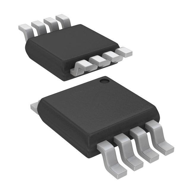
| 供应商器件封装 | 8-VSSOP |
| 其它名称 | 296-25648-6 |
| 包装 | Digi-Reel® |
| 压摆率 | 150 V/µs |
| 增益带宽积 | 100MHz |
| 安装类型 | 表面贴装 |
| 封装/外壳 | 8-TSSOP,8-MSOP(0.118",3.00mm 宽) |
| 工作温度 | -40°C ~ 125°C |
| 放大器类型 | 电压反馈 |
| 标准包装 | 1 |
| 电压-电源,单/双 (±) | 2.5 V ~ 5.5 V, ±1.25 V ~ 2.75 V |
| 电压-输入失调 | 2mV |
| 电流-电源 | 4.9mA |
| 电流-输入偏置 | 3pA |
| 电流-输出/通道 | 100mA |
| 电路数 | 2 |
| 输出类型 | 满摆幅 |


- 商务部:美国ITC正式对集成电路等产品启动337调查
- 曝三星4nm工艺存在良率问题 高通将骁龙8 Gen1或转产台积电
- 太阳诱电将投资9.5亿元在常州建新厂生产MLCC 预计2023年完工
- 英特尔发布欧洲新工厂建设计划 深化IDM 2.0 战略
- 台积电先进制程称霸业界 有大客户加持明年业绩稳了
- 达到5530亿美元!SIA预计今年全球半导体销售额将创下新高
- 英特尔拟将自动驾驶子公司Mobileye上市 估值或超500亿美元
- 三星加码芯片和SET,合并消费电子和移动部门,撤换高东真等 CEO
- 三星电子宣布重大人事变动 还合并消费电子和移动部门
- 海关总署:前11个月进口集成电路产品价值2.52万亿元 增长14.8%


PDF Datasheet 数据手册内容提取
Product Order Technical Tools & Support & Folder Now Documents Software Community OPA354A-Q1,OPA2354A-Q1,OPA4354-Q1 SBOS492F–JUNE2009–REVISEDMAY2018 OPAx354-Q1 250-MHz, Rail-to-Rail I/O, CMOS Operational Amplifiers 1 Features 3 Description • QualifiedforAutomotiveApplications The design of the OPAx354-Q1 family of high-speed, 1 voltage-feedback CMOS operational amplifiers is for • AEC-Q100QualifiedWiththeFollowingResults: video and other applications requiring wide – DeviceTemperatureGrade: –40°Cto+125°C bandwidth. These devices are unity-gain stable and AmbientOperatingTemperatureRange can drive large output currents. Differential gain is – DeviceHBMESDClassificationLevel2 0.02% and differential phase is 0.09°. Quiescent currentisonly4.9mAperchannel. – DeviceCDMESDClassificationLevel: The OPAx354-Q1 family of operational amplifiers (op- – C6forOPA354A-Q1andOPA2354A-Q1 amps) are optimized for operation on single or dual – C3forOPA4354-Q1 supplies as low as 2.5 V (±1.25 V) and up to 5.5 V • Unity-GainBandwidth:250MHz (±2.75 V). Common-mode input range extends • WideBandwidth:100-MHzGBWProduct beyond the supplies. The output swing is within 100 mVoftherails,supportingwidedynamicrange. • HighSlewRate:150V/μs The single-supply version (OPA354A-Q1) is available • LowNoise:6.5nV/√Hz in the tiny SOT–23-5 (DBV) package. The dual- • Rail-to-RailI/O supply version (OPA2354A-Q1) is available in the • HighOutputCurrent: >100mA miniature VSSOP-8 (DGK) package and features • ExcellentVideoPerformance completely independent circuitry for lowest crosstalk and freedom from interaction. The quad-supply – DifferentialGainError:0.02% version (OPA4354-Q1) is available in the TSSOP-14 – DifferentialPhaseError:0.09° (PW) package. The device specifications are for – 0.1-dBGainFlatness:40MHz operation over the automotive temperature range of –40°Cto+125°C. • LowInputBiasCurrent:3pA • QuiescentCurrent:4.9mA DeviceInformation(1) • ThermalShutdown PARTNUMBER PACKAGE(PIN) BODYSIZE(NOM) • SupplyRange:2.5Vto5.5V OPA354A-Q1 SOT-23(5) 2.90mm×1.60mm OPA2354A-Q1 VSSOP(8) 3.00mm×3.00mm 2 Applications OPA4354-Q1 TSSOP(14) 5.00mm×4.40mm • NavigationandRadioSystem (1) For all available packages, see the orderable addendum at • Blind-SpotDetection theendofthedatasheet. • Short-to-MidRangeRadar SimplifiedSchematic • VideoProcessing V+ • Ultrasound -In • OpticalNetworking,TunableLasers OPA354-Q1 V • PhotodiodeTransimpedanceAmplifiers OUT +In • ActiveFilters • High-SpeedIntegrators V- • Analog-to-DigitalConverter(ADC)InputBuffers • Digital-to-AnalogConverter(DAC)Output Amplifiers • BarcodeScanners • Communications 1 An IMPORTANT NOTICE at the end of this data sheet addresses availability, warranty, changes, use in safety-critical applications, intellectualpropertymattersandotherimportantdisclaimers.PRODUCTIONDATA.
OPA354A-Q1,OPA2354A-Q1,OPA4354-Q1 SBOS492F–JUNE2009–REVISEDMAY2018 www.ti.com Table of Contents 1 Features.................................................................. 1 7.4 DeviceFunctionalModes........................................20 2 Applications........................................................... 1 8 ApplicationandImplementation........................ 21 3 Description............................................................. 1 8.1 ApplicationInformation............................................21 4 RevisionHistory..................................................... 2 8.2 TypicalApplications................................................21 5 PinConfigurationandFunctions......................... 3 9 PowerSupplyRecommendations...................... 25 9.1 PowerDissipation...................................................26 6 Specifications......................................................... 6 10 Layout................................................................... 26 6.1 AbsoluteMaximumRatings......................................6 6.2 ESDRatings..............................................................6 10.1 LayoutGuidelines.................................................26 6.3 RecommendedOperatingConditions.......................6 10.2 LayoutExample....................................................27 6.4 ThermalInformation:OPA354A-Q1.........................6 11 DeviceandDocumentationSupport................. 28 6.5 ThermalInformation:OPA2354A-Q1.......................7 11.1 DocumentationSupport .......................................28 6.6 ThermalInformation:OPA4354A-Q1.......................7 11.2 RelatedLinks........................................................28 6.7 ElectricalCharacteristics...........................................8 11.3 ReceivingNotificationofDocumentationUpdates28 6.8 TypicalCharacteristics............................................10 11.4 CommunityResources..........................................28 7 DetailedDescription............................................ 15 11.5 Trademarks...........................................................28 7.1 Overview.................................................................15 11.6 ElectrostaticDischargeCaution............................29 7.2 FunctionalBlockDiagram.......................................15 11.7 Glossary................................................................29 7.3 FeatureDescription.................................................15 12 Mechanical,Packaging,andOrderable Information........................................................... 29 4 Revision History NOTE:Pagenumbersforpreviousrevisionsmaydifferfrompagenumbersinthecurrentversion. ChangesfromRevisionE(August2016)toRevisionF Page • DeletedtablenoteaboutinputterminalsandinputsignalsfromAbsoluteMaximumRatingstable .................................... 6 ChangesfromRevisionD(July2016)toRevisionE Page • Changedthegain-bandwidthproducttypicalvaluefrom10MHzbackto100MHzintheElectricalCharacteristicstable..8 ChangesfromRevisionC(June2016)toRevisionD Page • Changedthegain-bandwidthproducttypicalvaluefrom100MHzto10MHzintheElectricalCharacteristicstable...........8 • AddedtheReceivingNotificationofDocumentationUpdatesandCommunityResourcessections .................................. 28 ChangesfromRevisionB(December2014)toRevisionC Page • Added3additionalapplicationstotheApplicationssection.................................................................................................. 1 • UpdatedESDRatingstabletoshowCDMvalueforOPA354A-Q1andOPA2354A-Q1...................................................... 6 ChangesfromRevisionA(August2009)toRevisionB Page • AddedHandlingRatingtable,FeatureDescriptionsection,DeviceFunctionalModes,Applicationand Implementationsection,PowerSupplyRecommendationssection,Layoutsection,DeviceandDocumentation Supportsection,andMechanical,Packaging,andOrderableInformationsection................................................................ 1 • AddedtheOPA4354-Q1devicetothedatasheet ................................................................................................................ 1 2 SubmitDocumentationFeedback Copyright©2009–2018,TexasInstrumentsIncorporated ProductFolderLinks:OPA354A-Q1 OPA2354A-Q1 OPA4354-Q1
OPA354A-Q1,OPA2354A-Q1,OPA4354-Q1 www.ti.com SBOS492F–JUNE2009–REVISEDMAY2018 5 Pin Configuration and Functions OPA354A-Q1DBVPackage 5-PinSOT-23 TopView OUT 1 5 V+ V– 2 + +IN 3 4 –IN PinFunctions:OPA354A-Q1 PIN I/O DESCRIPTION NAME NO. +IN 3 I Noninvertinginput –IN 4 I Invertinginput OUT 1 O Output V+ 5 — Positive(highest)supply V– 2 — Negative(lowest)supply Copyright©2009–2018,TexasInstrumentsIncorporated SubmitDocumentationFeedback 3 ProductFolderLinks:OPA354A-Q1 OPA2354A-Q1 OPA4354-Q1
OPA354A-Q1,OPA2354A-Q1,OPA4354-Q1 SBOS492F–JUNE2009–REVISEDMAY2018 www.ti.com OPA2354A-Q1DGKPackage 8-PinVSSOP TopView OUT A 1 8 V+ –IN A 2 7 OUT B A +IN A 3 + 6 –IN B B V– 4 + 5 +IN B PinFunctions:OPA2354A-Q1 PIN I/O DESCRIPTION NAME NO. +INA 3 I Noninvertinginput,channelA +INB 5 I Noninvertinginput,channelB –INA 2 I Invertinginput,channelA –INB 6 I Invertinginput,channelB OUTA 1 O Output,channelA OUTB 7 O Output,channelB V+ 5 — Positive(highest)supply V– 2 — Negative(lowest)supply 4 SubmitDocumentationFeedback Copyright©2009–2018,TexasInstrumentsIncorporated ProductFolderLinks:OPA354A-Q1 OPA2354A-Q1 OPA4354-Q1
OPA354A-Q1,OPA2354A-Q1,OPA4354-Q1 www.ti.com SBOS492F–JUNE2009–REVISEDMAY2018 OPA4354-Q1PWPackage 14-PinTSSOP TopView OUT A 1 14 OUT D –IN A 2 – – 13 –IN D A D +IN A 3 + + 12 +IN D V+ 4 11 V– +IN B 5 10 +IN C B C –IN B 6 – – 9 –IN C OUT B 7 8 OUT C PinFunctions:OPA4354-Q1 PIN I/O DESCRIPTION NAME NO. +INA 3 I Noninvertinginput,channelA +INB 5 I Noninvertinginput,channelB +INC 10 I Noninvertinginput,channelC +IND 12 I Noninvertinginput,channelD –INA 2 I Invertinginput,channelA –INB 6 I Invertinginput,channelB –INC 9 I Invertinginput,channelC –IND 13 I Invertinginput,channelD OUTA 1 O Output,channelA OUTB 7 O Output,channelB OUTC 1 O Output,channelC OUTD 7 O Output,channelD V+ 5 — Positive(highest)supply V– 2 — Negative(lowest)supply Copyright©2009–2018,TexasInstrumentsIncorporated SubmitDocumentationFeedback 5 ProductFolderLinks:OPA354A-Q1 OPA2354A-Q1 OPA4354-Q1
OPA354A-Q1,OPA2354A-Q1,OPA4354-Q1 SBOS492F–JUNE2009–REVISEDMAY2018 www.ti.com 6 Specifications 6.1 Absolute Maximum Ratings overoperatingfree-airtemperaturerange(unlessotherwisenoted) (1) MIN MAX UNIT Supplyvoltage,V+toV–,V 7.5 V S Signalinputterminalsvoltage,V (V–)–0.5 (V+)+0.5 V IN Outputshort-circuitduration(2) Continuous Operatingtemperature,T –55 150 °C A Junctiontemperature,T 150 °C J Storagetemperature,T –65 150 °C stg (1) StressesbeyondthoselistedunderAbsoluteMaximumRatingsmaycausepermanentdamagetothedevice.Thesearestressratings only,whichdonotimplyfunctionaloperationofthedeviceattheseoranyotherconditionsbeyondthoseindicatedunderRecommended OperatingConditions.Exposuretoabsolute-maximum-ratedconditionsforextendedperiodsmayaffectdevicereliability. (2) Shortcircuittoground,oneamplifierperpackage 6.2 ESD Ratings VALUE UNIT OPA354A-Q1INDBV(SOT-23)PACKAGEANDOPA2354A-Q1INDGK(VSSOP)PACKAGE Humanbodymodel(HBM),perAECQ100-002(1) ±2000 V Electrostaticdischarge V (ESD) Chargeddevicemodel(CDM),perAECQ100-011 ±1000 OPA4354-Q1INPW(TSSOP)PACKAGE Humanbodymodel(HBM),perAECQ100-002(1) ±2000 V Electrostaticdischarge V (ESD) Chargeddevicemodel(CDM),perAECQ100-011 ±250 (1) AECQ100-002indicatesHBMstressingisdoneinaccordancewiththeANSI/ESDA/JEDECJS-001specification. 6.3 Recommended Operating Conditions overoperatingfree-airtemperaturerange(unlessotherwisenoted) MIN MAX UNIT V Supplyvoltage,V–toV+ 2.5 5.5 V S T Operatingfree-airtemperature –40 125 °C A 6.4 Thermal Information: OPA354A-Q1 OPA354A-Q1 OPA2354A-Q1 OPA4354-Q1 THERMALMETRIC(1) DBV(SOT-23) DGK(VSSOP) PW(TSSOP) UNIT 5PINS 8PINS 14PINS R Junction-to-ambientthermalresistance 216.3 175.9 92.6 °C/W θJA R Junction-to-case(top)thermalresistance 84.3 67.8 27.5 °C/W θJC(top) R Junction-to-boardthermalresistance 43.1 97.1 33.6 °C/W θJB ψ Junction-to-topcharacterizationparameter 3.8 9.3 1.9 °C/W JT ψ Junction-to-boardcharacterizationparameter 42.3 95.5 33.1 °C/W JB R Junction-to-case(bottom)thermalresistance N/A N/A N/A °C/W θJC(bot) (1) Formoreinformationabouttraditionalandnewthermalmetrics,seetheSemiconductorandICPackageThermalMetricsapplication report. 6 SubmitDocumentationFeedback Copyright©2009–2018,TexasInstrumentsIncorporated ProductFolderLinks:OPA354A-Q1 OPA2354A-Q1 OPA4354-Q1
OPA354A-Q1,OPA2354A-Q1,OPA4354-Q1 www.ti.com SBOS492F–JUNE2009–REVISEDMAY2018 6.5 Thermal Information: OPA2354A-Q1 OPA2354A-Q1 THERMALMETRIC(1) DGK(VSSOP) UNIT 8PINS R Junction-to-ambientthermalresistance 175.9 °C/W θJA R Junction-to-case(top)thermalresistance 67.8 °C/W θJC(top) R Junction-to-boardthermalresistance 97.1 °C/W θJB ψ Junction-to-topcharacterizationparameter 9.3 °C/W JT ψ Junction-to-boardcharacterizationparameter 95.5 °C/W JB R Junction-to-case(bottom)thermalresistance N/A °C/W θJC(bot) (1) Formoreinformationabouttraditionalandnewthermalmetrics,seetheSemiconductorandICPackageThermalMetricsapplication report. 6.6 Thermal Information: OPA4354A-Q1 OPA4354-Q1 THERMALMETRIC(1) PW(TSSOP) UNIT 14PINS R Junction-to-ambientthermalresistance 92.6 °C/W θJA R Junction-to-case(top)thermalresistance 27.5 °C/W θJC(top) R Junction-to-boardthermalresistance 33.6 °C/W θJB ψ Junction-to-topcharacterizationparameter 1.9 °C/W JT ψ Junction-to-boardcharacterizationparameter 33.1 °C/W JB R Junction-to-case(bottom)thermalresistance N/A °C/W θJC(bot) (1) Formoreinformationabouttraditionalandnewthermalmetrics,seetheSemiconductorandICPackageThermalMetricsapplication report. Copyright©2009–2018,TexasInstrumentsIncorporated SubmitDocumentationFeedback 7 ProductFolderLinks:OPA354A-Q1 OPA2354A-Q1 OPA4354-Q1
OPA354A-Q1,OPA2354A-Q1,OPA4354-Q1 SBOS492F–JUNE2009–REVISEDMAY2018 www.ti.com 6.7 Electrical Characteristics V =2.5Vto5.5V,R (feedbackresistor)=0Ω,R (loadresistor)=1kΩconnectedtoV /2(unlessotherwisenoted) S F L S PARAMETER TESTCONDITIONS MIN TYP MAX UNIT VOS Inputoffsetvoltage VVSCM==5(VV–)+0.8V TTAA==2F5u°llCrange ±2 ±1±08 mV ΔΔVTOS/ Otefmfspeetrvaotultraegedriftover TA=Fullrange ±4 μV/°C PSRR Offsetvoltagedriftvspower VS=2.7Vto5.5V, TA=25°C ±200 ±800 μV/V supply VCM=VS/2–0.15V TA=Fullrange ±900 IB Inputbiascurrent TA=25°C 3 ±50 pA IOS Inputoffsetcurrent TA=25°C ±1 ±50 pA Vn Inputvoltagenoisedensity f=1MHz,TA=25°C 6.5 nV/√Hz In Inputcurrentnoisedensity f=1MHz,TA=25°C 50 fA/√Hz Inputcommon-modevoltage VCM range TA=25°C (V–)–0.1 (V+)+0.1 V VS=5.5V TA=25°C 66 80 Inputcommon-moderejection –0.1V<VCM<3.5V TA=Fullrange 64 CMRR dB ratio VS=5.5V TA=25°C 56 68 –0.1V<VCM<5.6V TA=Fullrange 55 ZID Differentialinputimpedance TA=25°C 1013||2 Ω||pF Common-modeinput ZICM impedance TA=25°C 1013||2 Ω||pF VS=5V,0.3V<VO<4.7V 94 110 TA=25°C AOL Open-loopgain dB VS=5V,0.4V<VO<4.6V 90 TA=Fullrange G=1,VO=100mVp-p,RF=25Ω,TA=25°C 250 f–3dB Small-signalbandwidth MHz G=2,VO=100mVp-p,TA=25°C 90 G=10 GBW Gain-bandwidthproduct 100 MHz TA=25°C Bandwidthfor0.1-dBgain f0.1dB flatness G=2,VO=100mVp-p,TA=25°C 40 MHz VS=5V,G=1,4-Vstep,TA=25°C 150 SR Slewrate VS=5V,G=1,2-Vstep 130 V/μs VS=3V,G=1,2-Vstep 110 G=1,VO=200mVp-p,10%to90%,TA=25°C 2 trf Rise-and-falltime ns G=1,VO=2Vp-p,10%to90%,TA=25°C 11 tsettle Settlingtime VstSep=,5TAV,=G25=°C+1,2-Voutput 00..10%1% 3600 ns Overloadrecoverytime VIN×Gain=VS 5 ns TA=25°C Second-orderharmonic G=1,f=1MHz,VO=2Vp-p, distortion RL=200Ω,VCM=1.5V –75 dBc TA=25°C G=1,f=1MHz,VO=2Vp-p Third-orderharmonicdistortion RL=200Ω,VCM=1.5V –83 dBc TA=25°C Differentialgainerror NTSC,RL=150Ω,TA=25°C 0.02% Differentialphaseerror NTSC,RL=150Ω,TA=25°C 0.09 ° 8 SubmitDocumentationFeedback Copyright©2009–2018,TexasInstrumentsIncorporated ProductFolderLinks:OPA354A-Q1 OPA2354A-Q1 OPA4354-Q1
OPA354A-Q1,OPA2354A-Q1,OPA4354-Q1 www.ti.com SBOS492F–JUNE2009–REVISEDMAY2018 Electrical Characteristics (continued) V =2.5Vto5.5V,R (feedbackresistor)=0Ω,R (loadresistor)=1kΩconnectedtoV /2(unlessotherwisenoted) S F L S PARAMETER TESTCONDITIONS MIN TYP MAX UNIT Channel-to-channelcrosstalk (OPA2354A-Q1)(OPA4354- f=5MHz,TA=25°C –100 dB Q1) VS=5V,RL=1kΩ,AOL>94dB 0.1 0.3 TA=25°C Voltageoutputswingfromrail V VS=5V,RL=1kΩ 0.4 AOL>90dB,TA=Fullrange IO Outputcurrent(1)(2) VS=5V 100 mA VS=3V 50 Closed-loopoutputimpedance f<100kHz 0.05 Ω RO Open-loopoutputresistance 35 Ω Quiescentcurrent TA=25°C 4.9 6 IQ (peramplifier) VS=5V,IO=0,enabled TA=Fullrange 7.5 mA Thermalshutdownjunction Shutdown 160 °C temperature Resetfromshutdown 140 (1) SeetypicalcharacteristicgraphOutputVoltageSwingvsOutputCurrent(Figure20). (2) Notproductiontested Copyright©2009–2018,TexasInstrumentsIncorporated SubmitDocumentationFeedback 9 ProductFolderLinks:OPA354A-Q1 OPA2354A-Q1 OPA4354-Q1
OPA354A-Q1,OPA2354A-Q1,OPA4354-Q1 SBOS492F–JUNE2009–REVISEDMAY2018 www.ti.com 6.8 Typical Characteristics T =25°C,V =5V,R =0Ω,R =1kΩconnectedtoV /2(unlessotherwisenoted) A S F L S 3 3 V =0.1V G=1, V =0.1V ,R =604W O PP R =25W O PP F 0 F 0 B) G=+2,R =604W B) (d -3 F (d -3 n n Gai G=+5,RF=604W Gai G=-1 d -6 d -6 e e aliz G=+10,RF=604W aliz G=-5 G=-2 m -9 m -9 or or N N G=-10 -12 -12 -15 -15 100k 1M 10M 100M 1G 100k 1M 10M 100M 1G Frequency(Hz) Frequency(Hz) Figure1.NoninvertingSmall-SignalFrequencyResponse Figure2.InvertingSmall-SignalFrequencyResponse mV/div) mV/div) Voltage(40 Voltage(500 Output Output Time(20ns/div) Time(20ns/div) Figure3.NoninvertingSmall-SignalStepResponse Figure4.NoninvertingLarge-SignalStepResponse 0.5 -50 V =0.1V 0.4 O PP G=-1 0.3 c) -60 f=1MHz Gain(dB) 00..21 RGF==2+51W ortion(dB -70 RL=200W ed 0 Dist 2nd−Harmonic ormaliz --00..12 monic -80 N -0.3 RG==6+024W Har -90 F -0.4 3rd−Harmonic -0.5 -100 100k 1M 10M 100M 1G 0 1 2 3 4 Frequency(Hz) OutputVoltage(V ) PP Figure5.0.1-dBGainFlatness Figure6.HarmonicDistortionvsOutputVoltage 10 SubmitDocumentationFeedback Copyright©2009–2018,TexasInstrumentsIncorporated ProductFolderLinks:OPA354A-Q1 OPA2354A-Q1 OPA4354-Q1
OPA354A-Q1,OPA2354A-Q1,OPA4354-Q1 www.ti.com SBOS492F–JUNE2009–REVISEDMAY2018 Typical Characteristics (continued) T =25°C,V =5V,R =0Ω,R =1kΩconnectedtoV /2(unlessotherwisenoted) A S F L S -50 -50 V =2V V =2V O PP O PP f=1MHz f=1MHz Bc) -60 RL=200W Bc) -60 RL=200W d d ( ( n n ortio -70 2nd−Harmonic ortio -70 2nd−Harmonic st st Di Di c -80 c -80 ni ni mo mo 3rd−Harmonic Har -90 Har -90 3rd−Harmonic -100 -100 1 10 1 10 Gain(V/V) Gain(V/V) Figure7.HarmonicDistortionvsNoninvertingGain Figure8.HarmonicDistortionvsInvertingGain -50 -50 G=+1 G=+1 VO=2VPP VO=2VPP (dBc) -60 VRCLM==2010.5WV (dBc) -60 fV=CM1M=H1.z5V n n stortio -70 2nd−Harmonic stortio -70 2nd−Harmonic Di Di nic -80 nic -80 o o m m Har -90 3rd−Harmonic Har -90 3rd−Harmonic -100 -100 100k 1M 10M 100 1k Frequency(Hz) R (W) L Figure9.HarmonicDistortionvsFrequency Figure10.HarmonicDistortionvsLoadResistance 10k 3 R =10kW L 0 √VoltageHz),Noise(nV/√CurrHz)entNoise(fA/ 110100k VoltageNoise CurrentNoise NormalizedGain(dB) ---369 GRVCOFL====+0001pW.1FVPP RRRLLL===1150k00WWW -12 1 -15 10 100 1k 10k 100k 1M 10M 100M 100k 1M 10M 100M 1G Frequency(Hz) Frequency(Hz) Figure11.InputVoltageandCurrentNoiseSpectralDensity Figure12.FrequencyResponseforVariousRLValues vsFrequency Copyright©2009–2018,TexasInstrumentsIncorporated SubmitDocumentationFeedback 11 ProductFolderLinks:OPA354A-Q1 OPA2354A-Q1 OPA4354-Q1
OPA354A-Q1,OPA2354A-Q1,OPA4354-Q1 SBOS492F–JUNE2009–REVISEDMAY2018 www.ti.com Typical Characteristics (continued) T =25°C,V =5V,R =0Ω,R =1kΩconnectedtoV /2(unlessotherwisenoted) A S F L S 9 160 G=+1 For0.1dB 6 V =0.1V 140 ROS=0W PP CL=100pF Flatness B) 3 120 d ( n 0 100 ai G W) d -3 ( 80 alize -6 CL=47pF RS 60 Norm -9 40 VIN OPA354-Q1 RS VO -12 CL=5.6pF 20 CL 1kW -15 0 100k 1M 10M 100M 1G 1 10 100 1k Frequency(Hz) CapacitiveLoad(pF) Figure13.FrequencyResponseforVariousC Values Figure14.RecommendedR vsCapacitiveLoad L S 3 100 G=+1 C =5.6pF,R =0W L S 0 VO=0.1VPP CMRR 80 (dB) -3 CL=47pF,RS=140W dB) PSRR+ n ( Gai C =100pF,R =120W RR 60 ed -6 L S PS PSRR- Normaliz -9 VIN OPA354-Q1 RS VO CMRR, 40 -12 CL 1kW 20 -15 0 100k 1M 10M 100M 1G 10k 100k 1M 10M 100M 1G Frequency(Hz) Frequency(Hz) Figure15.FrequencyResponsevsCapacitiveLoad Figure16.Common-ModeRejectionRatioandPower- SupplyRejectionRatiovsFrequency 180 0.8 160 0.7 es) 140 e(degreain(dB) 112000 Phase gree) 00..65 asG 80 de dP en−LoopPhOpen−Loop 642000 Gain dG/dP(%/ 000...432 Op 0 -20 0.1 dG -40 0 10 100 1k 10k 100k 1M 10M 100M 1G 1 2 3 4 Frequency(Hz) Numberof150WLoads Figure17.Open-LoopGainandPhase Figure18.CompositeVideoDifferentialGainandPhase 12 SubmitDocumentationFeedback Copyright©2009–2018,TexasInstrumentsIncorporated ProductFolderLinks:OPA354A-Q1 OPA2354A-Q1 OPA4354-Q1
OPA354A-Q1,OPA2354A-Q1,OPA4354-Q1 www.ti.com SBOS492F–JUNE2009–REVISEDMAY2018 Typical Characteristics (continued) T =25°C,V =5V,R =0Ω,R =1kΩconnectedtoV /2(unlessotherwisenoted) A S F L S 10k 3 A) 1k nt(p e(V) 2 Curre100 Voltag 125°C 25°C –55°C Bias put ut Out 1 np 10 I 1 0 -55 -35 -15 5 25 45 65 85 105 125135 0 20 40 60 80 100 120 Temperature(°C) OutputCurrent(mA) V =3V S Figure19.InputBiasCurrentvsTemperature Figure20.OutputVoltageSwingvsOutputCurrent 7 5 6 V =5V 4 S mA) 5 (V) pplyCurrent( 43 VS=2.5V utputVoltage 32 125°C 25°C -55°C Su 2 O 1 1 0 0 -55 -35 -15 5 25 45 65 85 105 125135 0 25 50 75 100 125 150 175 200 Temperature(°C) OutputCurrent(mA) V =5V S Figure21.SupplyCurrentvsTemperature Figure22.OutputVoltageSwingvsOutputCurrent 100 6 V =5.5V S 5 W)e( 10 )VPP 4 MVaoxltiamguemWOithuotpuutt c ( Slew−Rate pedan 1 oltage 3 InducedDistortion m V V =2.7V OutputI 0.1 OPA354-Q1 Output 2 S 1 Z O 0.01 0 100k 1M 10M 100M 1G 1 10 100 Frequency(Hz) Frequency(MHz) Figure23.Closed-LoopOutputImpedancevsFrequency Figure24.MaximumOutputVoltagevsFrequency Copyright©2009–2018,TexasInstrumentsIncorporated SubmitDocumentationFeedback 13 ProductFolderLinks:OPA354A-Q1 OPA2354A-Q1 OPA4354-Q1
OPA354A-Q1,OPA2354A-Q1,OPA4354-Q1 SBOS492F–JUNE2009–REVISEDMAY2018 www.ti.com Typical Characteristics (continued) T =25°C,V =5V,R =0Ω,R =1kΩconnectedtoV /2(unlessotherwisenoted) A S F L S 0.5 120 0.4 VO=2VPP RL=1kW 0.3 110 B) %) 0.2 (d Error( 0.01 pGain100 Output --00..12 pen−Loo 90 O -0.3 80 -0.4 -0.5 70 0 10 20 30 40 50 60 70 80 90 100 -55 -35 -15 5 25 45 65 85 105 125135 Time(ns) Temperature(°C) Figure25.OutputSettlingTimeto0.1% Figure26.Open-LoopGainvsTemperature 100 90 B) d Common−ModeRejectionRatio on R( 80 Populati R,PSR 70 Power−SupplyRejectionRatio R M C 60 50 -8-7-6-5 -4-3 -2-1 0 1 2 3 4 5 6 7 8 -55 -35 -15 5 25 45 65 85 105 125135 OffsetVoltage(mV) Temperature(°C) Figure27.OffsetVoltageProductionDistribution Figure28.Common-ModeRejectionRatioandPower- SupplyRejectionRatiovsTemperature 0 B) -20 d ( d e err -40 ef R ut− -60 p n k,I -80 OPA2354-Q1 al st s Cro -100 -120 100k 1M 10M 100M 1G Frequency(Hz) Figure29.Channel-to-ChannelCrosstalk(OPAx354-Q1) 14 SubmitDocumentationFeedback Copyright©2009–2018,TexasInstrumentsIncorporated ProductFolderLinks:OPA354A-Q1 OPA2354A-Q1 OPA4354-Q1
OPA354A-Q1,OPA2354A-Q1,OPA4354-Q1 www.ti.com SBOS492F–JUNE2009–REVISEDMAY2018 7 Detailed Description 7.1 Overview The OPAx354-Q1 operational amplifiers are high-speed,150-V/μs, amplifiers making them excellent choices for transimpedance applications. The devices are unity-gain stable and can operate on a single-supply voltage (2.5 V to 5.5 V), or a split-supply voltage (±1.25 V to ±2.75 V), making them highly versatile and easy to use. The OPAx354A-Q1 amplifiers are specified from 2.5 V to 5.5 V and over the automotive temperature range of –40°C to+125°C. Table1.OPAx354-Q1RelatedProducts FEATURES PRODUCT ShutdownVersionofOPA354Family OPAx357 200-MHzGBW,Rail-to-RailOutput,CMOS,Shutdown OPAx355 200-MHzGBW,Rail-to-RailOutput,CMOS OPAx356 38-MHzGBW,Rail-to-RailInput/Output,CMOS OPAx350/3 75-MHzBW,G=2,Rail-to-RailOutput OPAx631 150-MHzBW,G=2,Rail-to-RailOutput OPAx634 100-MHzBW,DifferentialInput/Output,3.3-VSupply THS412x 7.2 Functional Block Diagram V+ Reference Current VIN+ VIN– VBIAS1 ClassAB Control V O Circuitry V BIAS2 V– (Ground) 7.3 Feature Description 7.3.1 OperatingVoltage The specifications of the OPAx354-Q1 family of devices apply over a power-supply range of 2.5 V to 5.5 V (±1.25 V to ±2.75 V). Supply voltages higher than 7.5 V (absolute maximum) can permanently damage the amplifier. The Typical Characteristics section of this data sheet shows the parameters that vary over supply voltage or temperature. Copyright©2009–2018,TexasInstrumentsIncorporated SubmitDocumentationFeedback 15 ProductFolderLinks:OPA354A-Q1 OPA2354A-Q1 OPA4354-Q1
OPA354A-Q1,OPA2354A-Q1,OPA4354-Q1 SBOS492F–JUNE2009–REVISEDMAY2018 www.ti.com Feature Description (continued) 7.3.2 Rail-to-RailInput The specified input common-mode voltage range of the OPAx354-Q1 family of devices extends 100 mV beyond the supply rails. A complementary input stage (an N-channel input differential pair in parallel with a P-channel differential pair) achieves this extension. The N-channel pair is active for input voltages close to the positive rail, typically (V+) – 1.2 V to 100 mV above the positive supply, while the P-channel pair is on for inputs from 100 mV below the negative supply to approximately (V+) – 1.2 V. A small transition region exists, typically (V+) – 1.5 V to (V+) – 0.9 V, in which both pairs are on. This 600-mV transition region can vary ±500 mV with process variation. As a result, the transition region (both input stages on) range from (V+) – 2 V to (V+) – 1.5 V on the low end, up to(V+) –0.9Vto(V+) – 0.4Vonthehighend. A double-folded cascode adds the signal from the two input pairs and presents a differential signal to the class- ABoutputstage. 7.3.3 Rail-to-RailOutput The device uses a class-AB output stage with common-source transistors to achieve rail-to-rail output. For high- impedance loads (> 200 Ω), the output voltage swing is typically 100 mV from the supply rails. With 10-Ω loads, a user can achieve a useful output swing while maintaining high open-loop gain; see Figure 20 (Output Voltage SwingvsOutputCurrent). 7.3.4 OutputDrive The OPAx354-Q1 output stage supplies a continuous output current of ±100 mA and still provide approximately 2.7-Voutputswingona5-Vsupply,asshowninFigure30. R 2 1 N(cid:159)(cid:3) + V 1 C (cid:16) 5 V 1 50 pF 1 µF R 1 10 N(cid:159)(cid:3) V+ OPA354-Q1 R V(cid:16) 3 V 10 N(cid:159)(cid:3) RSHUNT IN + 1 V In = 100 mA 1 (cid:159)(cid:3) R (cid:16) Out as shown 4 1 N(cid:159)(cid:3) LaserDiode Figure30. LaserDiodeDriver For maximum reliability, TI does not recommend running a continuous DC current greater than ±100 mA; see Figure 20 (Output Voltage Swing vs Output Current). Operate the OPAx354-Q1 family of devices in parallel to supplycontinuousoutputcurrentsgreaterthan ±100mA,asshowninFigure31. 16 SubmitDocumentationFeedback Copyright©2009–2018,TexasInstrumentsIncorporated ProductFolderLinks:OPA354A-Q1 OPA2354A-Q1 OPA4354-Q1
OPA354A-Q1,OPA2354A-Q1,OPA4354-Q1 www.ti.com SBOS492F–JUNE2009–REVISEDMAY2018 Feature Description (continued) R 2 10kW C 1 200pF +5V 1mF R 1 100kW R 5 1W OPA2354-Q1 R 3 100kW + - 2VIn=200mA R6 RSHUNT Out,asShown 1W 1W OPA2354-Q1 R 4 10kW LaserDiode Figure31. ParallelOperation The OPAx354-Q1 family of devices provides peak currents up to 200 mA, which correspond to the typical short- circuit current. Therefore, an on-chip thermal shutdown circuit protects the OPAx354-Q1 family of devices from dangerously high junction temperatures. At 160°C, the protection circuit shuts down the amplifier. Normal operationresumeswhenthejunctiontemperaturecoolsbelow140°C. 7.3.5 Video The OPAx354-Q1 output stage is capable of driving standard back-terminated 75-Ω video cables (see Figure 32). A back-terminated transmission line does not exhibit a capacitive load to the driver. A properly back- terminated 75-Ω cable does not appear as capacitance; the cable presents a 150-Ω resistive load to the OPAx354-Q1output. 5 V Video 75 (cid:159)(cid:3) In Video 75 (cid:159)(cid:3) OPA354-Q1 Output 2.5 V 604 (cid:159)(cid:3) 604 (cid:159)(cid:3) 2.5 V Figure32. Single-SupplyVideoLineDriver ThisseriesofamplifierscanbeusedasanamplifierforRGBgraphicsignals,whichhaveavoltageofzeroatthe videoblacklevelbyoffsettingandAC-couplingthesignal(seeFigure33). Copyright©2009–2018,TexasInstrumentsIncorporated SubmitDocumentationFeedback 17 ProductFolderLinks:OPA354A-Q1 OPA2354A-Q1 OPA4354-Q1
OPA354A-Q1,OPA2354A-Q1,OPA4354-Q1 SBOS492F–JUNE2009–REVISEDMAY2018 www.ti.com Feature Description (continued) 604 (cid:159)(cid:3) 3 V + 10 nF 1 µF V+ 604 (cid:159)(cid:3) 75 (cid:159)(cid:3) R 1/2 Red Red(1) 1 OPA2354-Q1 75 (cid:159)(cid:3) R 2 V+ R Green(1) 1 75 (cid:159)(cid:3) 1/2 Green R 604 (cid:159)(cid:3) OPA2354-Q1 2 75 (cid:159)(cid:3) 604 (cid:159)(cid:3) 604 (cid:159)(cid:3) 3 V + V+ 604 (cid:159)(cid:3) 1 µF 10 nF 75 (cid:159)(cid:3) R Blue Blue(1) 1 OPA354-Q1 75 (cid:159)(cid:3) R 2 (1) Sourcevideosignaloffset300mVabovegroundtoaccommodateopampswingtogroundcapability. Figure33. RGBCableDriver 7.3.6 DrivingAnalog-to-DigitalConverters The OPAx354-Q1 family of op-amps offers a 60-ns settling time to 0.01%, which makes the devices a viable option for driving high- and medium-speed sampling ADCs and reference circuits. The OPAx354-Q1 family of devices provides an effective means of buffering the input capacitance and resulting charge injection of the ADC while providing signal gain. The OPAx354-Q1 family of devices is designed for applications requiring high DC accuracy. Figure 34 shows the OPAx354-Q1 family of devices driving an ADC. With the OPAx354-Q1 family of devices in an inverting configuration, using a capacitor across the feedback resistor can filter high-frequency noise in the signal. 18 SubmitDocumentationFeedback Copyright©2009–2018,TexasInstrumentsIncorporated ProductFolderLinks:OPA354A-Q1 OPA2354A-Q1 OPA4354-Q1
OPA354A-Q1,OPA2354A-Q1,OPA4354-Q1 www.ti.com SBOS492F–JUNE2009–REVISEDMAY2018 Feature Description (continued) +5V 330pF 5kW 5kW V IN V+ VREF ADS7816,ADS7861, +In OPA354-Q1 orADS7864 +2.5V -In 12−BitA/DConverter GND VIN=0Vto-5Vfor0Vto5Voutput. NOTE:A/DConverterInput=0VtoVREF Figure34. OPA354A-Q1InvertingConfigurationDrivingtheADS7816 7.3.7 CapacitiveLoadandStability The OPAx354-Q1 family op amps can drive a wide range of capacitive loads. However, all op-amps under certain conditions can become unstable. Op amp configuration, gain, and load value are a few of the factors to consider when determining stability. An op amp in unity-gain configuration is most susceptible to the effects of capacitive loading. The capacitive load reacts with the output resistance of the op amp, along with any additional load resistance, to create a pole in the small-signal response that degrades the phase margin. For details, see Figure15(FrequencyResponsevsCapacitiveLoad.) The OPAx354-Q1 topology enhances the ability of the device to drive capacitive loads. In unity gain, these op- amps perform well with large capacitive loads. For details see Figure 14, Recommended R vs Capacitive Load, S andFigure15,FrequencyResponsevsCapacitiveLoad. Insert a 10-Ω to 20-Ω resistor in series with the output to improve capacitive laod drive in the unity-gain configuration, as shown in Figure 35. This configuration significantly reduces ringing with large capacitive loads; see Figure 15 (Frequency Response vs Capacitive Load.) However, if a resistive load is in parallel with the capacitive load, R creates a voltage divider. This configuration introduces a DC error at the output and slightly S reduces output swing. This error may be insignificant. For example, if R = 10 kΩ and R = 20 Ω, the error at the L S outputisapproximately0.2%. V+ R S OPA354-Q1 V OUT V IN R C L L Figure35. SeriesResistorinUnity-GainConfigurationImprovesCapacitiveLoadDrive 7.3.8 WidebandTransimpedanceAmplifier Wide bandwidth, low-input bias current, and low input voltage and current noise make the OPAx354-Q1 family of devices is designed as a wideband photodiode transimpedance amplifier for low-voltage single-supply applications. Low-voltage noise is important because photodiode capacitance causes the effective noise gain of thecircuittoincreaseathighfrequency. Copyright©2009–2018,TexasInstrumentsIncorporated SubmitDocumentationFeedback 19 ProductFolderLinks:OPA354A-Q1 OPA2354A-Q1 OPA4354-Q1
OPA354A-Q1,OPA2354A-Q1,OPA4354-Q1 SBOS492F–JUNE2009–REVISEDMAY2018 www.ti.com Feature Description (continued) The key elements to a transimpedance design, as shown in Figure 36, are the expected diode capacitance [including the parasitic input common-mode and differential-mode input capacitance (2 + 2) pF for the OPAx354- Q1],thedesiredtransimpedancegain(R ),andthegain-bandwidthproduct(GBW)fortheOPAx354-Q1familyof F devices (100 MHz). With these three variables set, the feedback capacitor value (C ) is set to control the F frequencyresponse. C F < 1 pF (preventsgainpeaking) R F 10 0(cid:159)(cid:3) +V O C OPA354-Q1 V D OUT Figure36. TransimpedanceAmplifier To achieve a maximally flat second-order Butterworth frequency response, set the feedback pole as shown in Equation1. 1 (cid:2) GBP 2(cid:1)R C (cid:1) 4(cid:1)R C F F F D (1) Typical surface-mount resistors have a parasitic capacitance of approximately 0.2 pF that required deduction fromthecalculatedfeedbackcapacitancevalue. UseEquation2tocalculatethebandwidth. (cid:3) GBP f(cid:1)3dB(cid:2) 2(cid:1)R C Hz F D (2) For even higher transimpedance bandwidth, use the high-speed CMOS OPA355-Q1 (200-MHz GBW) or the OPA655-Q1(400-MHzGBW). 7.4 Device Functional Modes The OPAx354-Q1 family of devices is powered on when the supply is connected. The devices operates as a single-supply operational amplifier or dual-supply amplifier depending on the application. The devices are used with asymmetrical supplies as long as the differential voltage (V– to V+) is at least 1.8 V and no greater than 5.5 V(example:V– setto–3.5VandV+setto1.5V). 20 SubmitDocumentationFeedback Copyright©2009–2018,TexasInstrumentsIncorporated ProductFolderLinks:OPA354A-Q1 OPA2354A-Q1 OPA4354-Q1
OPA354A-Q1,OPA2354A-Q1,OPA4354-Q1 www.ti.com SBOS492F–JUNE2009–REVISEDMAY2018 8 Application and Implementation NOTE Information in the following applications sections is not part of the TI component specification, and TI does not warrant its accuracy or completeness. TI’s customers are responsible for determining suitability of components for their purposes. Customers should validateandtesttheirdesignimplementationtoconfirmsystemfunctionality. 8.1 Application Information TheOPAx354-Q1familyofdevicesisaCMOS,rail-to-railI/O,high-speed,voltage-feedbackoperationalamplifier designed for video, high-speed, and other applications. The OPAx354-Q1 family of devices is available as a single,dual,orquadop-amp. Theamplifierfeaturesa100-MHzgainbandwidth,and150V/μsslewrate,butthedeviceisunity-gainstableand operatesasa1-V/Vvoltagefollower. 8.2 Typical Applications 8.2.1 TransimpedanceAmplifier Wide gain bandwidth, low input bias current, low input voltage, and current noise make the OPAx354-Q1 family of devices a preferred wideband photodiode transimpedance amplifier. Low-voltage noise is important because photodiodecapacitancecausestheeffectivenoisegainofthecircuittoincreaseathighfrequency. The key elements to a transimpedance design, as shown in Figure 37, are the expected diode capacitance (C ), which must include the parasitic input common-mode and differential-mode input capacitance (4 pF + 5 (D) pF); the desired transimpedance gain (R ); and the gain-bandwidth (GBW) for the OPAx354-Q1 family of (FB) devices (20 MHz). With these three variables set, the feedback capacitor value (C ) is set to control the (FB) frequency response. C includes the stray capacitance of R , which is 0.2 pF for a typical surface-mount (FB) (FB) resistor. (1) C (F) < 1 pF R (F) 10 MΩ V (V+) l C(D) OPA354-Q1 VO V (V–) (1) C isoptionaltopreventgainpeaking.C includesthestraycapacitanceofR . (FB) (FB) (FB) Figure37. Dual-SupplyTransimpedanceAmplifier 8.2.1.1 DesignRequirements PARAMETER VALUE SupplyvoltageV 2.5V (V+) SupplyvoltageV –2.5V (V–) Copyright©2009–2018,TexasInstrumentsIncorporated SubmitDocumentationFeedback 21 ProductFolderLinks:OPA354A-Q1 OPA2354A-Q1 OPA4354-Q1
OPA354A-Q1,OPA2354A-Q1,OPA4354-Q1 SBOS492F–JUNE2009–REVISEDMAY2018 www.ti.com 8.2.1.2 DetailedDesignProcedure Toachieveamaximally-flat,second-orderButterworthfrequencyresponse,thefeedbackpolemustbesetto: 1 GBW = 2´p´R ´C 4´p´R ´C (FB) (FB) (FB) (D) (3) UseEquation4tocalculatethebandwidth. GBW ƒ = (–3dB) 2´ p´R ´C (FB) (D) (4) For other transimpedance bandwidths, consider the high-speed CMOS OPA380 (90-MHz GBW), OPA354 (100- MHzGBW),OPA300 (180-MHzGBW),OPA355(200-MHzGBW),orOPA656andOPA657(400-MHzGBW). For single-supply applications, the +INx input can be biased with a positive DC voltage to allow the output to reach true zero when the photodiode is not exposed to any light, and respond without the added delay that results from coming out of the negative rail; this configuration is shown in Figure 38. This bias voltage appears acrossthephotodiode,providingareversebiasforfasteroperation. 0.5 pF 100 k(cid:13) – OPAx354-Q1 VOUT + SFH213 13.7 k(cid:13) 1 (cid:29)F 280 (cid:13) 5 V Figure38. Single-SupplyTransimpedanceAmplifier Foradditionalinformation,seetheCompensateTransimpedanceAmplifiersIntuitively applicationbulletin. 8.2.1.2.1 OptimizingTheTransimpedanceCircuit Toachievethebestperformance,componentsmustbeselectedaccordingtothefollowingguidelines: 1. For lowest noise, select R to create the total required gain. Using a lower value for R and adding gain (FB) (FB) after the transimpedance amplifier generally produces poorer noise performance. The noise produced by R increases with the square-root of R , whereas the signal increases linearly. Therefore, signal-to-noise (FB) (FB) ratioimproveswhenalltherequiredgainisplacedinthetransimpedancestage. 2. Minimize photodiode capacitance and stray capacitance at the summing junction (inverting input). This capacitance causes the voltage noise of the op amp to be amplified (increasing amplification at high frequency). Using a low-noise voltage source to reverse-bias a photodiode can significantly reduce the capacitance. Smaller photodiodes have lower capacitance. Use optics to concentrate light on a small photodiode. 3. Noise increases with increased bandwidth. Limit the circuit bandwidth to only that required. Use a capacitor acrosstheR tolimitbandwidth,evenifnotrequiredforstability. (FB) 4. Circuit board leakage can degrade the performance of an otherwise well-designed amplifier. Clean the circuit 22 SubmitDocumentationFeedback Copyright©2009–2018,TexasInstrumentsIncorporated ProductFolderLinks:OPA354A-Q1 OPA2354A-Q1 OPA4354-Q1
OPA354A-Q1,OPA2354A-Q1,OPA4354-Q1 www.ti.com SBOS492F–JUNE2009–REVISEDMAY2018 board carefully. A circuit board guard trace that encircles the summing junction and is driven at the same voltagecanhelpcontrolleakage. For additional information, see the Noise Analysis of FET Transimpedance Amplifiers, and Noise Analysis for High-SpeedOpAmps)applicationbulletins. 8.2.1.3 ApplicationCurve 105 100 95 90 A) B, V/ 85 d n ( 80 ai G 75 70 65 60 1000 10000 100000 1000000 1E+7 5E+7 Frequency (Hz) D001 –3dBbandwidthis4.56MHz Figure39. ACTransferFunction 8.2.2 High-ImpedanceSensorInterface Many sensors have high source impedances that may range up to 10 MΩ, or even higher. The output signal of sensors often must be amplified or otherwise conditioned by an amplifier. The input bias current of this amplifier canloadthesensoroutputandcauseavoltagedropacrossthesourceresistance,asshowninFigure40,where (V = V – I × R ). The last term, I × R , shows the voltage drop across R . To prevent errors (+INx) S (BIAS) (S) (BIAS) (S) (S) introduced to the system as a result of this voltage, use an op amp with low input bias current and high- impedance sensors. This low current keeps the error contribution by I × R less than the input voltage (BIAS) (S) noise of the amplifier, so that the amplifier does not become the dominant noise factor. The OPAx354-Q1 family ofdevicesseriesofopampsfeaturelowinputbiascurrent(typically200fA),andarethereforedesignedforsuch applications. R (S) 100 kΩ IIB V (+INx) V (V+) Device VO V(V–) R(F) R (G) Figure40. NoiseasaResultofI (BIAS) Copyright©2009–2018,TexasInstrumentsIncorporated SubmitDocumentationFeedback 23 ProductFolderLinks:OPA354A-Q1 OPA2354A-Q1 OPA4354-Q1
OPA354A-Q1,OPA2354A-Q1,OPA4354-Q1 SBOS492F–JUNE2009–REVISEDMAY2018 www.ti.com 8.2.3 DrivingADCs The OPAx354-Q1 op amps are designed for driving sampling analog-to-digital converters (ADCs) with sampling speeds up to 1 MSPS. The zero-crossover distortion input stage topology allows the OPAx354-Q1 family of devicestodriveADCswithoutdegradationofdifferentiallinearityandTHD. The OPAx354-Q1 family of devices can be used to buffer the ADC switched input capacitance and resulting charge injection while providing signal gain. Figure 41 shows the OPAx354-Q1 family of devices configured to drivetheADS8326. 5 V C1 100 nF 5 V R1(1) V(V+) 100Ω +INx OPAx354-Q1 ADS8326 V C3(1) 16-Bit (V–) 1 nF –INx 250kSPS V I 0 to 4.096 V REF IN Optional(2) 5 V R2 50 kΩ SD1 BAS40 –5 V REF3240 C2 4.096 V C4 100 nF 100 nF (1) Suggestedvalue;mayrequireadjustmentbasedonspecificapplication. (2) Single-supply applications lose a small number of ADC codes near ground as a result of op amp output swing limitation. If a negative powersupplyisavailable,thissimplecircuitcreatesa–0.3-Vsupplytoallowoutputswingtotruegroundpotential. Figure41. DrivingtheADS8326 8.2.4 ActiveFilter The OPAx354-Q1 family of devices is designed for active filter applications that require a wide bandwidth, fast slew rate, low-noise, single-supply operational amplifier. Figure 42 shows a 500 kHz, second-order, low-pass filter using the multiple-feedback (MFB) topology. The components are selected to provide a maximally-flat Butterworth response. Beyond the cutoff frequency, roll-off is –40 dB/dec. The Butterworth response is designed for applications requiring predictable gain characteristics, suchastheanti-aliasingfilterusedinfrontofanADC. One point to observe when considering the MFB filter is that the output is inverted relative to the input. If this inversion is not required, or not desired, a noninverting output can be achieved through one of the following options: 1. Addinganinvertingamplifier 2. Addinganadditionalsecond-orderMFBstage 3. Usinganoninvertingfiltertopology,suchastheSallen-Key(seeFigure43). MFB and Sallen-Key, low-pass and high-pass filter synthesis is accomplished using TI’s FilterPro™ program. Thissoftwareisavailableasafreedownloadonwww.ti.com. 24 SubmitDocumentationFeedback Copyright©2009–2018,TexasInstrumentsIncorporated ProductFolderLinks:OPA354A-Q1 OPA2354A-Q1 OPA4354-Q1
OPA354A-Q1,OPA2354A-Q1,OPA4354-Q1 www.ti.com SBOS492F–JUNE2009–REVISEDMAY2018 R3 549Ω C2 150 pF V R1 R2 (V+) 549Ω 1.24 kΩ V I Device VO C1 1 nF V(V–) Figure42. Second-OrderButterworth500-kHzLow-PassFilter 220 pF V (V+) 1.8kΩ 19.5kΩ 150 kΩ V=1 V I RMS 3.3 nF 47 pF Device VO V(V–) Figure43. OPAx354-Q1ConfiguredasaThree-Pole,20-kHz,Sallen-KeyFilter 9 Power Supply Recommendations The OPAx354-Q1 family of devices is specified for operation from 2.5 to 5.5 V (±1.25 to ±2.75 V); many specifications apply from –40°C to +125°C. Parameters that can exhibit significant variance with regard to operatingvoltageortemperatureareshownintheTypicalCharacteristicssection. CAUTION Supply voltages larger than 7.5 V can permanently damage the device (see the AbsoluteMaximumRatingstable). Place 0.1-μF bypass capacitors close to the power-supply pins to reduce errors coupling in from noisy or high- impedance power supplies. For more detailed information on bypass capacitor placement, see the Layout Guidelinessection. Copyright©2009–2018,TexasInstrumentsIncorporated SubmitDocumentationFeedback 25 ProductFolderLinks:OPA354A-Q1 OPA2354A-Q1 OPA4354-Q1
OPA354A-Q1,OPA2354A-Q1,OPA4354-Q1 SBOS492F–JUNE2009–REVISEDMAY2018 www.ti.com 9.1 Power Dissipation Power dissipation depends on power-supply voltage, signal and load conditions. With dc signals, power dissipation is equal to the product of output current times the voltage across the conducting output transistor (V – V ). Minimize power dissipation by using the lowest possible power-supply voltage required to ensure the S O requiredoutputvoltageswing. For resistive loads, the maximum power dissipation occurs at a DC output voltage of one-half the power-supply voltage. Dissipation with AC signals is lower. The Power Amplifier Stress and Power Handling Limitations application bulletin from www.ti.com explains how to calculate or measure power dissipation with unusual signals andloads. Any tendency to activate the thermal protection circuit indicates excessive power dissipation or an inadequate heat sink. For reliable operation, limit junction temperature to 150°C, maximum. To estimate the margin of safety in a complete design, increase the ambient temperature to trigger the thermal protection at 160°C. The thermal protectionmusttriggermorethan35°Cabovethemaximumexpectedambientconditionoftheapplication. 10 Layout 10.1 Layout Guidelines Use good high-frequency printed circuit board (PCB) layout techniques for the OPAx354-Q1 family of devices. Generous use of ground planes, short and direct signal traces, and a suitable bypass capacitor located at the V+ pin ensure clean, stable operation. Large areas of copper provide a means of dissipating heat that is generated in normal operation. Sockets are not recommended for use with any high-speed amplifier. A 10-nF ceramic bypass capacitor is the minimum recommended value; adding a 1-μF or larger tantalum capacitor in parallel can be beneficial when driving a low-resistance load. Providing adequate bypass capacitance is essential to achievingverylowharmonicandintermodulationdistortion. Forbestoperationalperformanceofthedevice,usegoodPCBlayoutpractices,including: • Noise can propagate into analog circuitry through the power pins of the circuit as a whole and the operational amplifier. Bypass capacitors are used to reduce the coupled noise by providing low- impedancepowersourceslocaltotheanalogcircuitry. – Connect low-ESR, 0.1-µF ceramic bypass capacitors between each supply pin and ground, placed as close to the device as possible. A single bypass capacitor from V+ to ground is applicable for single- supplyapplications. • Separate grounding for analog and digital portions of the circuitry is one of the simplest and most effective methods of noise suppression. One or more layers on multilayer PCBs are usually devoted to ground planes. A ground plane helps distribute heat and reduces EMI noise pickup. Make sure to physically separate digital and analog grounds, paying attention to the flow of the ground current. For moredetailedinformation,seeCircuitBoardLayoutTechniques. • To reduce parasitic coupling, run the input traces as far away from the supply or output traces as possible. If these traces cannot be kept separate, crossing the sensitive trace perpendicularly is much betterthancrossinginparallelwiththenoisytrace. • Place the external components as close to the device as possible. Keeping RF and RG close to the invertinginputminimizesparasiticcapacitance,asshowninFigure44. • Keep the length of input traces as short as possible. Always remember that the input traces are the most sensitivepartofthecircuit. • Consider a driven, low-impedance guard ring around the critical traces. A guard ring can significantly reduceleakagecurrentsfromnearbytracesthatareatdifferentpotentials. 26 SubmitDocumentationFeedback Copyright©2009–2018,TexasInstrumentsIncorporated ProductFolderLinks:OPA354A-Q1 OPA2354A-Q1 OPA4354-Q1
OPA354A-Q1,OPA2354A-Q1,OPA4354-Q1 www.ti.com SBOS492F–JUNE2009–REVISEDMAY2018 10.2 Layout Example Place components close Run the input traces to device and to each VS+ as far away from other to reduce parasitic the supply lines errors as possible RF NC NC Use a low-ESR, RG ceramic bypass GND –IN V+ capacitor VIN +IN OUTPUT V– NC GND VS– GND VOUT Ground (GND) plane on another layer Use low-ESR, ceramic bypass capacitor Figure44. OperationalAmplifierBoardLayoutforNoninvertingConfiguration Copyright©2009–2018,TexasInstrumentsIncorporated SubmitDocumentationFeedback 27 ProductFolderLinks:OPA354A-Q1 OPA2354A-Q1 OPA4354-Q1
OPA354A-Q1,OPA2354A-Q1,OPA4354-Q1 SBOS492F–JUNE2009–REVISEDMAY2018 www.ti.com 11 Device and Documentation Support 11.1 Documentation Support 11.1.1 RelatedDocumentation Forrelateddocumentationseethefollowing: • Texas Instruments, ADS8326 16-Bit, High-Speed, 2.7V to 5.5V microPower Sampling Analog-to-Digital Converter • TexasInstruments,CircuitBoardLayoutTechniques • TexasInstruments,CompensateTransimpedanceAmplifiersIntuitively • TexasInstruments,FilterPro™User'sGuide • TexasInstruments,NoiseAnalysisofFETTransimpedanceAmplifiers • TexasInstruments,NoiseAnalysisforHigh-SpeedOpAmps • TexasInstruments,OPA380andOPA2380 Precision,High-SpeedTransimpedanceAmplifier • Texas Instruments,OPA354, OPA2354, and OPA4354 250MHz, Rail-to-Rail I/O, CMOS Operational Amplifiers • TexasInstruments,OPA355,OPA2355,andOPA3355 200MHz,CMOSOperationalAmplifierWithShutdown • TexasInstruments,OPA656 Wideband,Unity-GainStable,FET-InputOperationalAmplifier • TexasInstruments,PowerAmplifierStressandPowerHandlingLimitations 11.2 Related Links The table below lists quick access links. Categories include technical documents, support and community resources,toolsandsoftware,andquickaccesstosampleorbuy. Table2.RelatedLinks TECHNICAL TOOLS& SUPPORT& PARTS PRODUCTFOLDER ORDERNOW DOCUMENTS SOFTWARE COMMUNITY OPA354A-Q1 Clickhere Clickhere Clickhere Clickhere Clickhere OPA2354A-Q1 Clickhere Clickhere Clickhere Clickhere Clickhere OPA4354-Q1 Clickhere Clickhere Clickhere Clickhere Clickhere 11.3 Receiving Notification of Documentation Updates To receive notification of documentation updates, navigate to the device product folder on ti.com. In the upper right corner, click on Alert me to register and receive a weekly digest of any product information that has changed.Forchangedetails,reviewtherevisionhistoryincludedinanyreviseddocument. 11.4 Community Resources The following links connect to TI community resources. Linked contents are provided "AS IS" by the respective contributors. They do not constitute TI specifications and do not necessarily reflect TI's views; see TI's Terms of Use. TIE2E™OnlineCommunity TI'sEngineer-to-Engineer(E2E)Community.Createdtofostercollaboration amongengineers.Ate2e.ti.com,youcanaskquestions,shareknowledge,exploreideasandhelp solveproblemswithfellowengineers. DesignSupport TI'sDesignSupport QuicklyfindhelpfulE2Eforumsalongwithdesignsupporttoolsand contactinformationfortechnicalsupport. 11.5 Trademarks E2EisatrademarkofTexasInstruments. FilterProisatrademarkofTexasInstrumentsIncorporated. Allothertrademarksarethepropertyoftheirrespectiveowners. 28 SubmitDocumentationFeedback Copyright©2009–2018,TexasInstrumentsIncorporated ProductFolderLinks:OPA354A-Q1 OPA2354A-Q1 OPA4354-Q1
OPA354A-Q1,OPA2354A-Q1,OPA4354-Q1 www.ti.com SBOS492F–JUNE2009–REVISEDMAY2018 11.6 Electrostatic Discharge Caution Thesedeviceshavelimitedbuilt-inESDprotection.Theleadsshouldbeshortedtogetherorthedeviceplacedinconductivefoam duringstorageorhandlingtopreventelectrostaticdamagetotheMOSgates. 11.7 Glossary SLYZ022—TIGlossary. Thisglossarylistsandexplainsterms,acronyms,anddefinitions. 12 Mechanical, Packaging, and Orderable Information The following pages include mechanical, packaging, and orderable information. This information is the most current data available for the designated devices. This data is subject to change without notice and revision of thisdocument.Forbrowser-basedversionsofthisdatasheet,refertotheleft-handnavigation. Copyright©2009–2018,TexasInstrumentsIncorporated SubmitDocumentationFeedback 29 ProductFolderLinks:OPA354A-Q1 OPA2354A-Q1 OPA4354-Q1
PACKAGE OPTION ADDENDUM www.ti.com 6-Feb-2020 PACKAGING INFORMATION Orderable Device Status Package Type Package Pins Package Eco Plan Lead/Ball Finish MSL Peak Temp Op Temp (°C) Device Marking Samples (1) Drawing Qty (2) (6) (3) (4/5) OPA2354AQDGKRQ1 ACTIVE VSSOP DGK 8 2500 Green (RoHS NIPDAU | NIPDAUAG Level-2-260C-1 YEAR -40 to 125 OSLQ & no Sb/Br) OPA354AQDBVRQ1 ACTIVE SOT-23 DBV 5 3000 Green (RoHS NIPDAU Level-2-260C-1 YEAR -40 to 125 OSFQ & no Sb/Br) OPA4354AQPWRQ1 ACTIVE TSSOP PW 14 2000 Green (RoHS NIPDAU Level-3-260C-168 HR -40 to 125 4354Q1 & no Sb/Br) (1) The marketing status values are defined as follows: ACTIVE: Product device recommended for new designs. LIFEBUY: TI has announced that the device will be discontinued, and a lifetime-buy period is in effect. NRND: Not recommended for new designs. Device is in production to support existing customers, but TI does not recommend using this part in a new design. PREVIEW: Device has been announced but is not in production. Samples may or may not be available. OBSOLETE: TI has discontinued the production of the device. (2) RoHS: TI defines "RoHS" to mean semiconductor products that are compliant with the current EU RoHS requirements for all 10 RoHS substances, including the requirement that RoHS substance do not exceed 0.1% by weight in homogeneous materials. Where designed to be soldered at high temperatures, "RoHS" products are suitable for use in specified lead-free processes. TI may reference these types of products as "Pb-Free". RoHS Exempt: TI defines "RoHS Exempt" to mean products that contain lead but are compliant with EU RoHS pursuant to a specific EU RoHS exemption. Green: TI defines "Green" to mean the content of Chlorine (Cl) and Bromine (Br) based flame retardants meet JS709B low halogen requirements of <=1000ppm threshold. Antimony trioxide based flame retardants must also meet the <=1000ppm threshold requirement. (3) MSL, Peak Temp. - The Moisture Sensitivity Level rating according to the JEDEC industry standard classifications, and peak solder temperature. (4) There may be additional marking, which relates to the logo, the lot trace code information, or the environmental category on the device. (5) Multiple Device Markings will be inside parentheses. Only one Device Marking contained in parentheses and separated by a "~" will appear on a device. If a line is indented then it is a continuation of the previous line and the two combined represent the entire Device Marking for that device. (6) Lead/Ball Finish - Orderable Devices may have multiple material finish options. Finish options are separated by a vertical ruled line. Lead/Ball Finish values may wrap to two lines if the finish value exceeds the maximum column width. Important Information and Disclaimer:The information provided on this page represents TI's knowledge and belief as of the date that it is provided. TI bases its knowledge and belief on information provided by third parties, and makes no representation or warranty as to the accuracy of such information. Efforts are underway to better integrate information from third parties. TI has taken and continues to take reasonable steps to provide representative and accurate information but may not have conducted destructive testing or chemical analysis on incoming materials and chemicals. TI and TI suppliers consider certain information to be proprietary, and thus CAS numbers and other limited information may not be available for release. Addendum-Page 1
PACKAGE OPTION ADDENDUM www.ti.com 6-Feb-2020 In no event shall TI's liability arising out of such information exceed the total purchase price of the TI part(s) at issue in this document sold by TI to Customer on an annual basis. OTHER QUALIFIED VERSIONS OF OPA4354-Q1 : •Catalog: OPA4354 NOTE: Qualified Version Definitions: •Catalog - TI's standard catalog product Addendum-Page 2
PACKAGE MATERIALS INFORMATION www.ti.com 3-Nov-2018 TAPE AND REEL INFORMATION *Alldimensionsarenominal Device Package Package Pins SPQ Reel Reel A0 B0 K0 P1 W Pin1 Type Drawing Diameter Width (mm) (mm) (mm) (mm) (mm) Quadrant (mm) W1(mm) OPA2354AQDGKRQ1 VSSOP DGK 8 2500 330.0 12.4 5.3 3.4 1.4 8.0 12.0 Q1 OPA354AQDBVRQ1 SOT-23 DBV 5 3000 179.0 8.4 3.2 3.2 1.4 4.0 8.0 Q3 OPA4354AQPWRQ1 TSSOP PW 14 2000 330.0 12.4 6.9 5.6 1.6 8.0 12.0 Q1 PackMaterials-Page1
PACKAGE MATERIALS INFORMATION www.ti.com 3-Nov-2018 *Alldimensionsarenominal Device PackageType PackageDrawing Pins SPQ Length(mm) Width(mm) Height(mm) OPA2354AQDGKRQ1 VSSOP DGK 8 2500 367.0 367.0 35.0 OPA354AQDBVRQ1 SOT-23 DBV 5 3000 195.0 200.0 45.0 OPA4354AQPWRQ1 TSSOP PW 14 2000 367.0 367.0 35.0 PackMaterials-Page2
PACKAGE OUTLINE DBV0005A SOT-23 - 1.45 mm max height SCALE 4.000 SMALL OUTLINE TRANSISTOR C 3.0 2.6 0.1 C 1.75 1.45 1.45 B A 0.90 PIN 1 INDEX AREA 1 5 2X 0.95 3.05 2.75 1.9 1.9 2 4 3 0.5 5X 0.3 0.15 0.2 C A B (1.1) TYP 0.00 0.25 GAGE PLANE 0.22 TYP 0.08 8 TYP 0.6 0 0.3 TYP SEATING PLANE 4214839/E 09/2019 NOTES: 1. All linear dimensions are in millimeters. Any dimensions in parenthesis are for reference only. Dimensioning and tolerancing per ASME Y14.5M. 2. This drawing is subject to change without notice. 3. Refernce JEDEC MO-178. 4. Body dimensions do not include mold flash, protrusions, or gate burrs. Mold flash, protrusions, or gate burrs shall not exceed 0.15 mm per side. www.ti.com
EXAMPLE BOARD LAYOUT DBV0005A SOT-23 - 1.45 mm max height SMALL OUTLINE TRANSISTOR PKG 5X (1.1) 1 5 5X (0.6) SYMM (1.9) 2 2X (0.95) 3 4 (R0.05) TYP (2.6) LAND PATTERN EXAMPLE EXPOSED METAL SHOWN SCALE:15X SOLDER MASK SOLDER MASK METAL UNDER METAL OPENING OPENING SOLDER MASK EXPOSED METAL EXPOSED METAL 0.07 MAX 0.07 MIN ARROUND ARROUND NON SOLDER MASK SOLDER MASK DEFINED DEFINED (PREFERRED) SOLDER MASK DETAILS 4214839/E 09/2019 NOTES: (continued) 5. Publication IPC-7351 may have alternate designs. 6. Solder mask tolerances between and around signal pads can vary based on board fabrication site. www.ti.com
EXAMPLE STENCIL DESIGN DBV0005A SOT-23 - 1.45 mm max height SMALL OUTLINE TRANSISTOR PKG 5X (1.1) 1 5 5X (0.6) SYMM 2 (1.9) 2X(0.95) 3 4 (R0.05) TYP (2.6) SOLDER PASTE EXAMPLE BASED ON 0.125 mm THICK STENCIL SCALE:15X 4214839/E 09/2019 NOTES: (continued) 7. Laser cutting apertures with trapezoidal walls and rounded corners may offer better paste release. IPC-7525 may have alternate design recommendations. 8. Board assembly site may have different recommendations for stencil design. www.ti.com
None
None
None
None
IMPORTANTNOTICEANDDISCLAIMER TI PROVIDES TECHNICAL AND RELIABILITY DATA (INCLUDING DATASHEETS), DESIGN RESOURCES (INCLUDING REFERENCE DESIGNS), APPLICATION OR OTHER DESIGN ADVICE, WEB TOOLS, SAFETY INFORMATION, AND OTHER RESOURCES “AS IS” AND WITH ALL FAULTS, AND DISCLAIMS ALL WARRANTIES, EXPRESS AND IMPLIED, INCLUDING WITHOUT LIMITATION ANY IMPLIED WARRANTIES OF MERCHANTABILITY, FITNESS FOR A PARTICULAR PURPOSE OR NON-INFRINGEMENT OF THIRD PARTY INTELLECTUAL PROPERTY RIGHTS. These resources are intended for skilled developers designing with TI products. You are solely responsible for (1) selecting the appropriate TI products for your application, (2) designing, validating and testing your application, and (3) ensuring your application meets applicable standards, and any other safety, security, or other requirements. These resources are subject to change without notice. TI grants you permission to use these resources only for development of an application that uses the TI products described in the resource. Other reproduction and display of these resources is prohibited. No license is granted to any other TI intellectual property right or to any third party intellectual property right. TI disclaims responsibility for, and you will fully indemnify TI and its representatives against, any claims, damages, costs, losses, and liabilities arising out of your use of these resources. TI’s products are provided subject to TI’s Terms of Sale (www.ti.com/legal/termsofsale.html) or other applicable terms available either on ti.com or provided in conjunction with such TI products. TI’s provision of these resources does not expand or otherwise alter TI’s applicable warranties or warranty disclaimers for TI products. Mailing Address: Texas Instruments, Post Office Box 655303, Dallas, Texas 75265 Copyright © 2020, Texas Instruments Incorporated