ICGOO在线商城 > 集成电路(IC) > 线性 - 放大器 - 仪表,运算放大器,缓冲器放大器 > OPA2171AIDCUR
 Datasheet下载
- 型号: OPA2171AIDCUR
- 制造商: Texas Instruments
- 库位|库存: xxxx|xxxx
- 要求:
| 数量阶梯 | 香港交货 | 国内含税 |
| +xxxx | $xxxx | ¥xxxx |
查看当月历史价格
查看今年历史价格
OPA2171AIDCUR产品简介:
ICGOO电子元器件商城为您提供OPA2171AIDCUR由Texas Instruments设计生产,在icgoo商城现货销售,并且可以通过原厂、代理商等渠道进行代购。 OPA2171AIDCUR价格参考。Texas InstrumentsOPA2171AIDCUR封装/规格:线性 - 放大器 - 仪表,运算放大器,缓冲器放大器, 通用 放大器 2 电路 满摆幅 US8。您可以下载OPA2171AIDCUR参考资料、Datasheet数据手册功能说明书,资料中有OPA2171AIDCUR 详细功能的应用电路图电压和使用方法及教程。
Texas Instruments(德州仪器)的OPA2171AIDCUR是一款双通道、低噪声、精密运算放大器,适用于多种应用场景。以下是其主要应用领域:

 1. 工业自动化与控制
在工业自动化系统中,OPA2171AIDCUR可用于信号调理电路,处理来自传感器的微弱信号。例如,在温度、压力或位移传感器的应用中,它能够将传感器输出的微小电压变化放大到适合后续处理的电平。由于其低噪声特性,OPA2171AIDCUR可以确保信号在放大过程中不失真,从而提高系统的测量精度。

 2. 医疗设备
在医疗电子设备中,如心电图(ECG)、脑电图(EEG)等生物电信号监测设备,OPA2171AIDCUR能够精确放大这些微弱的生物电信号。它的低噪声和高共模抑制比(CMRR)特性,使得它可以有效抑制环境噪声和电源干扰,确保采集到的信号具有高信噪比,进而提高诊断的准确性。

 3. 音频处理
在高端音频设备中,OPA2171AIDCUR可以用作前置放大器,放大来自麦克风或其他音频源的信号。其低失真和低噪声性能有助于保持音频信号的纯净度,提供更清晰、更真实的音质表现。此外,它还可以用于有源滤波器设计,帮助实现音频信号的频带选择和处理。

 4. 测试与测量仪器
在精密测试与测量仪器中,如示波器、频谱分析仪等,OPA2171AIDCUR可用于前端信号放大。它能够处理从毫伏级到伏特级的信号变化,并且保持高线性度和稳定性,确保测量结果的准确性和可靠性。

 5. 通信设备
在通信系统中,特别是无线通信设备的射频前端,OPA2171AIDCUR可用于中频信号放大。它能够在较低功耗下提供稳定的增益,同时保持低噪声水平,这对于提高通信质量至关重要。

 总结
OPA2171AIDCUR凭借其低噪声、高精度和低功耗的特点,广泛应用于工业自动化、医疗设备、音频处理、测试与测量仪器以及通信设备等领域。它能够为各种精密信号处理任务提供可靠的解决方案,确保信号的完整性和准确性。
| 参数 | 数值 |
| -3db带宽 | - |
| 产品目录 | 集成电路 (IC)半导体 |
| 描述 | IC OPAMP GP 3MHZ RRO US8运算放大器 - 运放 36V,MICROPOWER,RRO GEN PURP OP AMP |
| 产品分类 | Linear - Amplifiers - Instrumentation, OP Amps, Buffer Amps集成电路 - IC |
| 品牌 | Texas Instruments |
| 产品手册 | http://www.ti.com/litv/sbos516d |
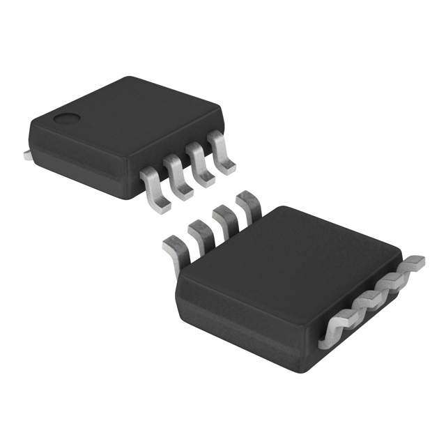
| 产品图片 |
|
| rohs | 符合RoHS无铅 / 符合限制有害物质指令(RoHS)规范要求 |
| 产品系列 | 放大器 IC,运算放大器 - 运放,Texas Instruments OPA2171AIDCUR- |
| 数据手册 | 点击此处下载产品Datasheethttp://www.ti.com/lit/pdf/slyb174 |
| 产品型号 | OPA2171AIDCUR |
| 产品种类 | 运算放大器 - 运放 |
| 供应商器件封装 | US8 |
| 共模抑制比—最小值 | 104 dB |
| 关闭 | No Shutdown |
| 其它名称 | 296-29399-6 |
| 包装 | Digi-Reel® |
| 压摆率 | 1.5 V/µs |
| 商标 | Texas Instruments |
| 增益带宽生成 | 3 MHz |
| 增益带宽积 | 3MHz |
| 安装类型 | 表面贴装 |
| 安装风格 | SMD/SMT |
| 封装 | Reel |
| 封装/外壳 | 8-VFSOP(0.091",2.30mm 宽) |
| 封装/箱体 | VSSOP-8 |
| 工作温度 | -40°C ~ 125°C |
| 工作电源电压 | 2.7 V to 36 V, +/- 1.35 V to +/- 18 V |
| 工厂包装数量 | 3000 |
| 放大器类型 | 通用 |
| 最大工作温度 | + 125 C |
| 最小双重电源电压 | +/- 1.35 V |
| 最小工作温度 | - 40 C |
| 标准包装 | 1 |
| 电压-电源,单/双 (±) | 2.7 V ~ 36 V, ±1.35 V ~ 18 V |
| 电压-输入失调 | 250µV |
| 电流-电源 | 475µA |
| 电流-输入偏置 | 8pA |
| 电流-输出/通道 | 35mA |
| 电源电流 | 0.475 mA |
| 电路数 | 2 |
| 系列 | OPA2171 |
| 设计资源 | http://www.digikey.com/product-highlights/cn/zh/texas-instruments-webench-design-center/3176 |
| 转换速度 | 1.5 V/us |
| 输入偏压电流—最大 | 15 pA |
| 输入参考电压噪声 | 3 nV |
| 输入补偿电压 | 1.8 mV |
| 输出电流 | 25 mA |
| 输出类型 | 满摆幅 |
| 通道数量 | 2 Channel |


- 商务部:美国ITC正式对集成电路等产品启动337调查
- 曝三星4nm工艺存在良率问题 高通将骁龙8 Gen1或转产台积电
- 太阳诱电将投资9.5亿元在常州建新厂生产MLCC 预计2023年完工
- 英特尔发布欧洲新工厂建设计划 深化IDM 2.0 战略
- 台积电先进制程称霸业界 有大客户加持明年业绩稳了
- 达到5530亿美元!SIA预计今年全球半导体销售额将创下新高
- 英特尔拟将自动驾驶子公司Mobileye上市 估值或超500亿美元
- 三星加码芯片和SET,合并消费电子和移动部门,撤换高东真等 CEO
- 三星电子宣布重大人事变动 还合并消费电子和移动部门
- 海关总署:前11个月进口集成电路产品价值2.52万亿元 增长14.8%


PDF Datasheet 数据手册内容提取
Product Order Technical Tools & Support & Reference Folder Now Documents Software Community Design OPA171,OPA2171,OPA4171 SBOS516F–SEPTEMBER2010–REVISEDAPRIL2018 OPAx171 36-V, Single-Supply, SOT-553, General-Purpose Operational Amplifiers 1 Features 3 Description • SupplyRange:2.7to36V, ±1.35Vto±18V The OPA171, OPA2171, and OPA4171 (OPAx171) 1 are a family of 36-V, single-supply, low-noise • LowNoise:14nV/√Hz operational amplifiers with the ability to operate on • LowOffsetDrift: ±0.3 µV/°C(Typical) supplies ranging from 2.7 V (±1.35 V) to 36 V (±18 • RFIFilteredInputs V). These devices are available in micro-packages and offer low offset, drift, and bandwidth with low • InputRangeIncludesTheNegativeSupply quiescent current. The single, dual, and quad • InputRangeOperatesToPositiveSupply versions all have identical specifications for maximum • Rail-to-RailOutput designflexibility. • GainBandwidth:3MHz Unlike most operational amplifiers, which are • LowQuiescentCurrent:475µAperAmplifier specified at only one supply voltage, the OPAx171 family is specified from 2.7 to 36 V. Input signals • HighCommon-ModeRejection:120dB(Typical) beyond the supply rails do not cause phase reversal. • Low-InputBiasCurrent:8pA The OPAx171 family is stable with capacitive loads • Industry-StandardPackages: up to 300 pF. The input can operate 100 mV below – 8-PinSOIC the negative rail and within 2 V of the top rail during normal operation. These devices can operate with full – 8-PinMSOP rail-to-rail input 100 mV beyond the top rail, but with – 14-PinTSSOP reducedperformancewithin2Vofthetoprail. • microPackages: The OPAx171 series of operational amplifiers are – SingleinSOT-553 specifiedfrom–40°Cto+125°C. – DualinVSSOP-8 DeviceInformation(1) 2 Applications PARTNUMBER PACKAGE BODYSIZE(NOM) OPA171 SOT-23(5) 1.60mm×2.90mm • TrackingAmplifierinPowerModules OPA2171 SOIC(8) 3.90mm×4.90mm • MerchantPowerSupplies TSSOP(14) 4.40mm×5.00mm • TransducerAmplifiers OPA4171 SOIC(14) 3.90mm×8.65mm • BridgeAmplifiers (1) For all available packages, see the orderable addendum at • TemperatureMeasurements theendofthedatasheet. • StrainGaugeAmplifiers • PrecisionIntegrators • Battery-PoweredInstruments • TestEquipment SPACE OffsetVoltagevsCommon-ModeVoltage OffsetVoltagevsPowerSupply 1000 350 10Typical Units Shown V = ±2.25 V to±18 V 800 SUPPLY 250 10Typical Units Shown 600 400 150 V) 200 V) 50 m m ( 0 ( S S O O -50 V -200 V -400 -150 -600 -250 -800 V = -18.1 V CM -1000 -350 -20 -15 -10 -5 0 5 10 15 20 0 2 4 6 8 10 12 14 16 18 20 V (V) V (V) CM SUPPLY 1 An IMPORTANT NOTICE at the end of this data sheet addresses availability, warranty, changes, use in safety-critical applications, intellectualpropertymattersandotherimportantdisclaimers.PRODUCTIONDATA.
OPA171,OPA2171,OPA4171 SBOS516F–SEPTEMBER2010–REVISEDAPRIL2018 www.ti.com Table of Contents 1 Features.................................................................. 1 7.2 FunctionalBlockDiagram.......................................18 2 Applications........................................................... 1 7.3 FeatureDescription.................................................18 3 Description............................................................. 1 7.4 DeviceFunctionalModes........................................20 4 RevisionHistory..................................................... 2 8 ApplicationandImplementation........................ 21 8.1 ApplicationInformation............................................21 5 PinConfigurationandFunctions......................... 4 8.2 TypicalApplication .................................................23 6 Specifications......................................................... 7 9 PowerSupplyRecommendations...................... 27 6.1 AbsoluteMaximumRatings......................................7 10 Layout................................................................... 27 6.2 ESDRatings..............................................................7 6.3 RecommendedOperatingConditions.......................7 10.1 LayoutGuidelines ................................................27 6.4 ThermalInformation:OPA171..................................8 10.2 LayoutExample....................................................27 6.5 ThermalInformation:OPA2171................................8 11 DeviceandDocumentationSupport................. 28 6.6 ThermalInformation:OPA4171................................8 11.1 RelatedLinks........................................................28 6.7 ElectricalCharacteristics...........................................9 11.2 CommunityResources..........................................28 6.8 TypicalCharacteristics:TableofGraphs................11 11.3 Trademarks...........................................................28 6.9 TypicalCharacteristics ...........................................12 11.4 ElectrostaticDischargeCaution............................28 7 DetailedDescription............................................ 18 11.5 Glossary................................................................28 7.1 Overview.................................................................18 12 Mechanical,Packaging,andOrderable Information........................................................... 28 4 Revision History NOTE:Pagenumbersforpreviousrevisionsmaydifferfrompagenumbersinthecurrentversion. ChangesfromRevisionE(April2015)toRevisionF Page • Changedminimumsupplyvoltagevaluefrom±20Vto0VinAbsoluteMaximumRatingstable ....................................... 7 • Addedmaximumsupplyvoltagevalueof40VtoAbsoluteMaximumRatingstable ........................................................... 7 • RewroteElectricalOverstresssubsectioncontentinApplicationInformationsection ........................................................ 21 ChangesfromRevisionD(September2012)toRevisionE Page • Changeddevicetitle(removed"ValueLineSeries").............................................................................................................. 1 • AddedESDRatingstable,FeatureDescriptionsection,DeviceFunctionalModes,ApplicationandImplementation section,PowerSupplyRecommendationssection,Layoutsection,DeviceandDocumentationSupportsection,and Mechanical,Packaging,andOrderableInformationsection ................................................................................................. 1 ChangesfromRevisionC(June2011)toRevisionD Page • Added"ValueLineSeries"totitle........................................................................................................................................... 1 ChangesfromRevisionB(November2010)toRevisionC Page • AddedMSOP-8packagetodevicegraphic........................................................................................................................... 1 • AddedMSOP-8packagetoFeaturesbullets......................................................................................................................... 1 • AddedMSOP-8packagetoProductFamilytable.................................................................................................................. 1 • UpdatedpinoutconfigurationsforOPA2171andOPA4171.................................................................................................. 4 • AddedMSOP-8packagetoOPA2171ThermalInformationtable......................................................................................... 8 • AddednewrowforVoltageOutputSwingfromRailparametertoOutputsubsectionofElectricalCharacteristics............10 • ChangedVoltageOutputSwingfromRailparametertoovertemperatureinOutputsubsectionofElectrical Characteristics...................................................................................................................................................................... 10 • ChangedFigure9................................................................................................................................................................. 12 2 SubmitDocumentationFeedback Copyright©2010–2018,TexasInstrumentsIncorporated ProductFolderLinks:OPA171 OPA2171 OPA4171
OPA171,OPA2171,OPA4171 www.ti.com SBOS516F–SEPTEMBER2010–REVISEDAPRIL2018 ChangesfromRevisionA(November,2010)toRevisionB Page • Changedinputoffsetvoltagespecification............................................................................................................................. 9 • Changedinputoffsetvoltage,overtemperaturespecification............................................................................................... 9 • Changedquiescentcurrentperamplifier,overtemperaturespecification........................................................................... 10 Copyright©2010–2018,TexasInstrumentsIncorporated SubmitDocumentationFeedback 3 ProductFolderLinks:OPA171 OPA2171 OPA4171
OPA171,OPA2171,OPA4171 SBOS516F–SEPTEMBER2010–REVISEDAPRIL2018 www.ti.com 5 Pin Configuration and Functions OPA171DRLPackage 5-PinSOT-553 TopView IN+ 1 5 V+ V- 2 IN- 3 4 OUT OPA171DBVPackage 5-PinSOT-23 TopView OUT 1 5 V+ V- 2 +IN 3 4 -IN OPA171DPackage 8-PinSOIC TopView NC(1) 1 8 NC(1) -IN 2 7 V+ +IN 3 6 OUT V- 4 5 NC(1) (1) NC-nointernalconnection PinFunctions:OPA171 PIN I/O DESCRIPTION NAME DRL DBV D +IN 1 3 3 I Noninvertinginput –IN 3 4 2 I Invertinginput OUT 4 1 6 O Output V+ 5 5 7 — Positive(highest)supply V– 2 2 4 — Negative(lowest)supply NC — — 1,5,8 — Nointernalconnection(canbeleftfloating) 4 SubmitDocumentationFeedback Copyright©2010–2018,TexasInstrumentsIncorporated ProductFolderLinks:OPA171 OPA2171 OPA4171
OPA171,OPA2171,OPA4171 www.ti.com SBOS516F–SEPTEMBER2010–REVISEDAPRIL2018 OPA2171D,DCU,andDCKPackages 8-PinSO,VSSOPandMSOP TopView OUT A 1 8 V+ -IN A 2 7 OUT B +IN A 3 6 -IN B V- 4 5 +IN B PinFunctions:OPA2171 PIN I/O DESCRIPTION NAME NO. +INA 3 I Noninvertinginput +INB 5 I Noninvertinginput –INA 2 I Invertinginput –INB 6 O Invertinginput OUTA 1 O Output OUTB 7 — Output V+ 8 — Positive(highest)supply V– 4 — Negative(lowest)supply Copyright©2010–2018,TexasInstrumentsIncorporated SubmitDocumentationFeedback 5 ProductFolderLinks:OPA171 OPA2171 OPA4171
OPA171,OPA2171,OPA4171 SBOS516F–SEPTEMBER2010–REVISEDAPRIL2018 www.ti.com OPA4171DandPWPackages 14-PinSOandTSSOP TopView OUT A 1 14 OUT D -IN A 2 13 -IN D +IN A 3 12 +IN D V+ 4 11 V- +IN B 5 10 +IN C -IN B 6 9 -IN C OUT B 7 8 OUT C PinFunctions:OPA4171 PIN I/O DESCRIPTION NAME NO. +INA 3 I Noninvertinginput +INB 5 I Noninvertinginput +INC 10 I Noninvertinginput +IND 12 I Noninvertinginput –INA 2 I Invertinginput –INB 6 I Invertinginput –INC 9 I Invertinginput –IND 13 I Invertinginput OUTA 1 O Output OUTB 7 O Output OUTC 8 O Output OUTD 14 O Output V+ 4 — Positive(highest)supply V– 11 — Negative(lowest)supply 6 SubmitDocumentationFeedback Copyright©2010–2018,TexasInstrumentsIncorporated ProductFolderLinks:OPA171 OPA2171 OPA4171
OPA171,OPA2171,OPA4171 www.ti.com SBOS516F–SEPTEMBER2010–REVISEDAPRIL2018 6 Specifications 6.1 Absolute Maximum Ratings overoperatingfree-airtemperaturerange,(unlessotherwisenoted) (1) MIN MAX UNIT Supplyvoltage 0 40 V Voltage (V–)–0.5 (V+)+0.5 V Signalinputterminals Current –10 10 mA Outputshortcircuit(2) Continuous Operatingtemperature –55 150 °C Junctiontemperature 150 °C Storagetemperature –65 150 °C (1) StressesbeyondthoselistedunderAbsoluteMaximumRatingsmaycausepermanentdamagetothedevice.Thesearestressratings only,whichdonotimplyfunctionaloperationofthedeviceattheseoranyotherconditionsbeyondthoseindicatedunderRecommended OperatingConditions.Exposuretoabsolute-maximum-ratedconditionsforextendedperiodsmayaffectdevicereliability. (2) Short-circuittoground,oneamplifierperpackage. 6.2 ESD Ratings VALUE UNIT Electrostatic Human-bodymodel(HBM),perANSI/ESDA/JEDECJS-001(1) ±4000 V V (ESD) discharge Charged-devicemodel(CDM),perJEDECspecificationJESD22-C101(2) ±750 (1) JEDECdocumentJEP155statesthat500-VHBMallowssafemanufacturingwithastandardESDcontrolprocess. (2) JEDECdocumentJEP157statesthat250-VCDMallowssafemanufacturingwithastandardESDcontrolprocess. 6.3 Recommended Operating Conditions overoperatingfree-airtemperaturerange(unlessotherwisenoted) MIN NOM MAX UNIT Supplyvoltage(V+–V–) 4.5(±2.25) 36(±18) V Specifiedtemperature –40 125 °C Copyright©2010–2018,TexasInstrumentsIncorporated SubmitDocumentationFeedback 7 ProductFolderLinks:OPA171 OPA2171 OPA4171
OPA171,OPA2171,OPA4171 SBOS516F–SEPTEMBER2010–REVISEDAPRIL2018 www.ti.com 6.4 Thermal Information: OPA171 OPA171 THERMALMETRIC(1) D(SO) DBV(SOT-23) DRL(SOT-553) UNIT 8PINS 5PINS 5PINS RθJA Junction-to-ambientthermalresistance 149.5 245.8 208.1 °C/W RθJC(top) Junction-to-case(top)thermalresistance 97.9 133.9 0.1 °C/W RθJB Junction-to-boardthermalresistance 87.7 83.6 42.4 °C/W ψJT Junction-to-topcharacterizationparameter 35.5 18.2 0.5 °C/W ψJB Junction-to-boardcharacterizationparameter 89.5 83.1 42.2 °C/W RθJC(bot) Junction-to-case(bottom)thermalresistance N/A N/A N/A °C/W (1) Formoreinformationabouttraditionalandnewthermalmetrics,seetheSemiconductorandICPackageThermalMetricsapplication report. 6.5 Thermal Information: OPA2171 OPA2171 THERMALMETRIC(1) D(SO) DGK(MSOP) DCU(VSSOP) UNIT 8PINS 8PINS 8PINS RθJA Junction-to-ambientthermalresistance 134.3 175.2 195.3 °C/W RθJC(top) Junction-to-case(top)thermalresistance 72.1 74.9 59.4 °C/W RθJB Junction-to-boardthermalresistance 60.6 22.2 115.1 °C/W ψJT Junction-to-topcharacterizationparameter 18.2 1.6 4.7 °C/W ψJB Junction-to-boardcharacterizationparameter 53.8 22.8 114.4 °C/W RθJC(bot) Junction-to-case(bottom)thermalresistance N/A N/A N/A °C/W (1) Formoreinformationabouttraditionalandnewthermalmetrics,seetheSemiconductorandICPackageThermalMetricsapplication report. 6.6 Thermal Information: OPA4171 OPA4171 THERMALMETRIC(1) D(SOIC) PW(TSSOP) UNIT 14PINS 14PINS RθJA Junction-to-ambientthermalresistance 93.2 106.9 °C/W RθJC(top) Junction-to-case(top)thermalresistance 51.8 24.4 °C/W RθJB Junction-to-boardthermalresistance 49.4 59.3 °C/W ψJT Junction-to-topcharacterizationparameter 13.5 0.6 °C/W ψJB Junction-to-boardcharacterizationparameter 42.2 54.3 °C/W RθJC(bot) Junction-to-case(bottom)thermalresistance N/A N/A °C/W (1) Formoreinformationabouttraditionalandnewthermalmetrics,seetheSemiconductorandICPackageThermalMetricsapplication report. 8 SubmitDocumentationFeedback Copyright©2010–2018,TexasInstrumentsIncorporated ProductFolderLinks:OPA171 OPA2171 OPA4171
OPA171,OPA2171,OPA4171 www.ti.com SBOS516F–SEPTEMBER2010–REVISEDAPRIL2018 6.7 Electrical Characteristics atT =25°C,V =2.7to36V,V =V =V /2,andR =10kΩconnectedtoV /2,(unlessotherwisenoted) A S CM OUT S LOAD S PARAMETER TESTCONDITIONS MIN TYP MAX UNIT OFFSETVOLTAGE V Inputoffsetvoltage 0.25 ±1.8 mV OS Overtemperature T =–40°Cto+125°C 0.3 ±2 mV A dV /dT Drift T =–40°Cto+125°C 0.3 ±2 µV/°C OS A V =4to36V vspowersupply S 1 ±3 µV/V T =–40°Cto+125°C A Channelseparation,DC DC 5 µV/V INPUTBIASCURRENT Inputbiascurrent ±8 ±15 pA I B Overtemperature T =–40°Cto+125°C ±3.5 nA A Inputoffsetcurrent ±4 pA I OS Overtemperature T =–40°Cto+125°C ±3.5 nA A NOISE Inputvoltagenoise f=0.1Hzto10Hz 3 µV PP f=100Hz 25 nV/√Hz e Inputvoltagenoisedensity n f=1kHz 14 nV/√Hz INPUTVOLTAGE V Common-modevoltagerange(1) (V–)–0.1 (V+)–2V V CM V V =±2V S (V–)–0.1V<V <(V+)–2V 90 104 dB CM T =–40°Cto+125°C A CMRR Common-moderejectionratio V =±18V S (V–)–0.1V<V <(V+)–2V 104 120 dB CM T =–40°Cto+125°C A INPUTIMPEDANCE Differential 100||3 MΩ||pF 1012Ω|| Common-mode 6||3 pF OPEN-LOOPGAIN V =4Vto36V S A Open-loopvoltagegain (V–)+0.35V<V <(V+)–0.35V 110 130 dB OL O T =–40°Cto+125°C A FREQUENCYRESPONSE GBP Gainbandwidthproduct 3 MHz SR Slewrate G=1 1.5 V/µs To0.1% V =±18V,G=1 6 µs S 10-Vstep t Settlingtime S To0.01%(12bit) V =±18V,G=1 10 µs S 10-Vstep Overloadrecoverytime V ×gain>V 2 µs IN S G=1,f=1kHz THD+N Totalharmonicdistortion+noise 0.0002% V =3V O RMS OUTPUT (1) Theinputrangecanbeextendedbeyond(V+)–2VuptoV+.SeeTypicalCharacteristicsandApplicationandImplementationfor additionalinformation. Copyright©2010–2018,TexasInstrumentsIncorporated SubmitDocumentationFeedback 9 ProductFolderLinks:OPA171 OPA2171 OPA4171
OPA171,OPA2171,OPA4171 SBOS516F–SEPTEMBER2010–REVISEDAPRIL2018 www.ti.com Electrical Characteristics (continued) atT =25°C,V =2.7to36V,V =V =V /2,andR =10kΩconnectedtoV /2,(unlessotherwisenoted) A S CM OUT S LOAD S PARAMETER TESTCONDITIONS MIN TYP MAX UNIT V =5V Voltageoutputswingfromrail S 30 mV R =10kΩ L VO RL=10kΩ (V–)+ (V+)– Overtemperature A ≥110dB V OL 0.35 0.35 T =–40°Cto+125°C A I Short-circuitcurrent +25/–35 mA SC C Capacitiveloaddrive SeeTypicalCharacteristics pF LOAD f=1MHz R Open-loopoutputresistance 150 Ω O I =0A O POWERSUPPLY V Specifiedvoltagerange 2.7 36 V S Quiescentcurrentperamplifier I =0A 475 595 µA O IQ Overtemperature IO=0A 650 µA T =–40°Cto+125°C A TEMPERATURE Specifiedrange –40 125 °C Operatingrange –55 150 °C 10 SubmitDocumentationFeedback Copyright©2010–2018,TexasInstrumentsIncorporated ProductFolderLinks:OPA171 OPA2171 OPA4171
OPA171,OPA2171,OPA4171 www.ti.com SBOS516F–SEPTEMBER2010–REVISEDAPRIL2018 6.8 Typical Characteristics: Table of Graphs Table1.CharacteristicPerformanceMeasurements DESCRIPTION FIGURE OffsetVoltageProductionDistribution Figure1 OffsetVoltageDriftDistribution Figure2 OffsetVoltagevsTemperature Figure3 OffsetVoltagevsCommon-ModeVoltage Figure4 OffsetVoltagevsCommon-ModeVoltage(UpperStage) Figure5 OffsetVoltagevsPowerSupply Figure6 I andI vsCommon-ModeVoltage Figure7 B OS InputBiasCurrentvsTemperature Figure8 OutputVoltageSwingvsOutputCurrent(MaximumSupply) Figure9 CMRRandPSRRvsFrequency(Referred-toInput) Figure10 CMRRvsTemperature Figure11 PSRRvsTemperature Figure12 0.1-Hzto10-HzNoise Figure13 InputVoltageNoiseSpectralDensityvsFrequency Figure14 THD+NRatiovsFrequency Figure15 THD+NvsOutputAmplitude Figure16 QuiescentCurrentvsTemperature Figure17 QuiescentCurrentvsSupplyVoltage Figure18 Open-LoopGainandPhasevsFrequency Figure19 Closed-LoopGainvsFrequency Figure20 Open-LoopGainvsTemperature Figure21 Open-LoopOutputImpedancevsFrequency Figure22 Small-SignalOvershootvsCapacitiveLoad(100-mVOutputStep) Figure23,Figure24 NoPhaseReversal Figure25 PositiveOverloadRecovery Figure26 NegativeOverloadRecovery Figure27 Small-SignalStepResponse(100mV) Figure28,Figure29 Large-SignalStepResponse Figure30,Figure31 Large-SignalSettlingTime(10-VPositiveStep) Figure32 Large-SignalSettlingTime(10-VNegativeStep) Figure33 Short-CircuitCurrentvsTemperature Figure34 MaximumOutputVoltagevsFrequency Figure35 ChannelSeparationvsFrequency Figure36 Copyright©2010–2018,TexasInstrumentsIncorporated SubmitDocumentationFeedback 11 ProductFolderLinks:OPA171 OPA2171 OPA4171
OPA171,OPA2171,OPA4171 SBOS516F–SEPTEMBER2010–REVISEDAPRIL2018 www.ti.com 6.9 Typical Characteristics V =±18V,V =V /2,R =10kΩconnectedtoV /2,andC =100pF,(unlessotherwisenoted) S CM S LOAD S L 16 25 Distribution Taken From 3500 Amplifiers Distribution Taken From 110 Amplifiers 14 age of Amplifiers (%) 112086 ge of Amplifiers (%) 211050 cent 4 enta Per erc 5 2 P 0 0000000000000000000000000 0 120110100-90-80-70-60-50-40-30-20-10 102030405060708090100110120 00.10.20.30.40.50.60.70.80.911.11.21.31.41.51.61.71.81.92 --- Offset Voltage (mV) Offset Voltage Drift (mV/°C) Figure1.OffsetVoltageProductionDistribution Figure2.OffsetVoltageDriftDistribution 600 1000 5 Typical Units Shown 10Typical Units Shown 800 400 600 V) 200 400 m age ( 0 mV) 200 et Volt -200 V(OS -2000 s Off -400 -400 -600 -600 -800 V = -18.1 V CM -800 -1000 -75 -50 -25 0 25 50 75 100 125 150 -20 -15 -10 -5 0 5 10 15 20 Temperature (°C) V (V) CM Figure3.OffsetVoltagevsTemperature Figure4.OffsetVoltagevsCommon-ModeVoltage 10000 350 10Typical Units Shown V = ±2.25 V to±18 V 8000 SUPPLY 250 10Typical Units Shown 6000 4000 150 V) 2000 V) 50 m m ( 0 ( S S O O -50 V -2000 V Normal -4000 Operation -150 V = 18.1 V CM -6000 -250 -8000 -10000 -350 15.5 16 16.5 17 17.5 18 18.5 0 2 4 6 8 10 12 14 16 18 20 V (V) V (V) CM SUPPLY Figure5.OffsetVoltagevsCommon-ModeVoltage(Upper Figure6.OffsetVoltagevsPowerSupply Stage) 12 SubmitDocumentationFeedback Copyright©2010–2018,TexasInstrumentsIncorporated ProductFolderLinks:OPA171 OPA2171 OPA4171
OPA171,OPA2171,OPA4171 www.ti.com SBOS516F–SEPTEMBER2010–REVISEDAPRIL2018 Typical Characteristics (continued) V =±18V,V =V /2,R =10kΩconnectedtoV /2,andC =100pF,(unlessotherwisenoted) S CM S LOAD S L 15 10000 14 -IB IB+ 111321 +-IIOBS pA) 1000 IIBO-S IB A) 10 nt ( p 9 e 100 d I(OS 87 s Curr an 6 Bia 10 IB 54 nput IOS 3 V =-18.1V V = 16V I 1 2 CM CM 1 0 0 -20 -18 -12 -6 0 6 12 18 20 -40 -25 0 25 50 75 100 125 V (V) Temperature (°C) CM Figure7.I andI vsCommon-ModeVoltage Figure8.InputBiasCurrentvsTemperature B OS 18 140 Output Voltage (V) -11---44111111..76555567 -+++42810552°5°°CCC°C Common-Mode Rejection Ratio (dB),Power-Supply Rejection Ratio (dB) 11208642000000 +-CPPMSSRRRRRR -18 0 0 2 4 6 8 10 12 14 16 1 10 100 1k 10k 100k 1M 10M Output Current (mA) Frequency (Hz) Figure9.OutputVoltageSwingvsOutputCurrent Figure10.CMRRandPSRRvsFrequency(Referred-to (MaximumSupply) Input) 30 3 mode Rejection Ratio (V/V) -2110000 mply Rejection Ratio (V/V) -2101 M p mmon- -20 VVSS== 24.V7V wer-Su -2 VS= 2.7V to 36V Co VS= 36V Po VS= 4V to 36V -30 -3 -75 -50 -25 0 25 50 75 100 125 150 -75 -50 -25 0 25 50 75 100 125 150 Temperature (°C) Temperature (°C) Figure11.CMRRvsTemperature Figure12.PSRRvsTemperature Copyright©2010–2018,TexasInstrumentsIncorporated SubmitDocumentationFeedback 13 ProductFolderLinks:OPA171 OPA2171 OPA4171
OPA171,OPA2171,OPA4171 SBOS516F–SEPTEMBER2010–REVISEDAPRIL2018 www.ti.com Typical Characteristics (continued) V =±18V,V =V /2,R =10kΩconnectedtoV /2,andC =100pF,(unlessotherwisenoted) S CM S LOAD S L 1000 )z H Ö V/ n y ( 100 div nsit 1V/m e De s oi N 10 e g a olt V 1 Time (1s/div) 1 10 100 1k 10k 100k 1M Frequency (Hz) Figure13.0.1-Hzto10-HzNoise Figure14.InputVoltageNoiseSpectralDensityvs Frequency 0.01 -80 0.1 -80 %) VOUT= 3VRMS To%) BW = 80kHz To se ( BW = 80kHz tal Hse ( tal H Noi armNoi 0.01 arm onic Distortion + 0.00.000011 --110200 onic Distortion +onic Distortion + 0.001 --110200 onic Distortion + Total Harm 0.00001 GG == -+11,, RRLL== 21k0WkW -140 Noise (dB)Total Harm 0.00.00000011 GG == -+11,, RRLL== 21k0WkW -140 Noise (dB) 10 100 1k 10k 20k 0.01 0.1 1 10 20 Frequency (Hz) Output Amplitude (V ) RMS Figure15.THD+NRatiovsFrequency Figure16.THD+NvsOutputAmplitude 0.65 0.6 0.55 0.6 0.5 0.55 A) A) 0.45 m 0.5 m ( ( IQ IQ 0.4 0.45 0.35 0.4 0.3 Specified Supply-Voltage Range 0.35 0.25 -75 -50 -25 0 25 50 75 100 125 150 0 4 8 12 16 20 24 28 32 36 Temperature (°C) Supply Voltage (V) Figure17.QuiescentCurrentvsTemperature Figure18.QuiescentCurrentvsSupplyVoltage 14 SubmitDocumentationFeedback Copyright©2010–2018,TexasInstrumentsIncorporated ProductFolderLinks:OPA171 OPA2171 OPA4171
OPA171,OPA2171,OPA4171 www.ti.com SBOS516F–SEPTEMBER2010–REVISEDAPRIL2018 Typical Characteristics (continued) V =±18V,V =V /2,R =10kΩconnectedtoV /2,andC =100pF,(unlessotherwisenoted) S CM S LOAD S L 180 180 25 Gain 20 135 135 15 Phase 10 B) 90 90 P B) Gain (d 45 45 hase ()° Gain (d 50 -5 0 0 -10 G = 10 -15 G = 1 G =-1 -45 -45 -20 1 10 100 1k 10k 100k 1M 10M 10k 100k 1M 10M 100M Frequency (Hz) Frequency (Hz) Figure19.Open-LoopGainandPhasevsFrequency Figure20.Closed-LoopGainvsFrequency 3 1M 5Typical Units Shown V = 2.7 V S 2.5 VS= 4 V 100k V = 36 V S 10k 2 V) mV/ 1.5 W() 1k ( O OL Z 100 A 1 10 0.5 1 0 1m -40 -25 0 25 50 75 100 125 1 10 100 1k 10k 100k 1M 10M Temperature (°C) Frequency (Hz) Figure21.Open-LoopGainvsTemperature Figure22.Open-LoopOutputImpedancevsFrequency 50 50 R = 0 W 45 45 OUT R = 25 W 40 40 OUT R = 50 W 35 35 OUT %) %) ot ( 30 ot ( 30 ho 25 ho 25 s s er 20 er 20 Ov 11505 RRROOOUUUTTT=== 02550ΩΩΩ TLV-1118781 -VQV1 ROUT GRL = C1L Ov 11505 RI=10 kW RTFLV1=187 11 -VQ01 kW GROU T= -1CL -18 V 0 0 0 100 200 300 400 500 600 700 800 900 1000 0 100 200 300 400 500 600 700 800 900 1000 Capacitive Load (pF) Capacitive Load (pF) Figure23.Small-SignalOvershootvsCapacitiveLoad Figure24.Small-SignalOvershootvsCapacitiveLoad (100-mVOutputStep) (100-mVOutputStep) Copyright©2010–2018,TexasInstrumentsIncorporated SubmitDocumentationFeedback 15 ProductFolderLinks:OPA171 OPA2171 OPA4171
OPA171,OPA2171,OPA4171 SBOS516F–SEPTEMBER2010–REVISEDAPRIL2018 www.ti.com Typical Characteristics (continued) V =±18V,V =V /2,R =10kΩconnectedtoV /2,andC =100pF,(unlessotherwisenoted) S CM S LOAD S L 18 V Output TLV171-Q1 VOUT -18 V 3S7in Ve PWPave div (±18.5 V) div VIN V/ V/ 5 5 20kW 2kW +18V Output OPA171 VOUT VIN -18V G =-10 Time (100ms/div) Time (5ms/div) Figure25.NoPhaseReversal Figure26.PositiveOverloadRecovery RL= 10kW +18V G = +1 C = 100pF L OPA171 -18V RL CL v VIN div V/di mV/ 5 0 20kW 2 2kW +18V OPA171 VOUT V VIN OUT -18V G =-10 Time (5ms/div) Time (1ms/div) Figure27.NegativeOverloadRecovery Figure28.Small-SignalStepResponse(100mV) C = 100pF L v mV/di RI=2kW RF=2kW V/div 20 +18V 2 OPA171 CL -18V G =-1 Time (20ms/div) Time (5ms/div) Figure29.Small-SignalStepResponse(100mV) Figure30.Large-SignalStepResponse 16 SubmitDocumentationFeedback Copyright©2010–2018,TexasInstrumentsIncorporated ProductFolderLinks:OPA171 OPA2171 OPA4171
OPA171,OPA2171,OPA4171 www.ti.com SBOS516F–SEPTEMBER2010–REVISEDAPRIL2018 Typical Characteristics (continued) V =±18V,V =V /2,R =10kΩconnectedtoV /2,andC =100pF,(unlessotherwisenoted) S CM S LOAD S L 10 8 V) 6 m e ( 4 12-Bit Settling V/div al Valu 20 2 n m Fi -2 (±1/2LSB =±0.024%) Fro -4 D -6 -8 -10 Time (4ms/div) 0 4 8 12 16 20 24 28 32 36 Time (ms) Figure31.Large-SignalStepResponse Figure32.Large-SignalSettlingTime(10-VPositiveStep) 10 50 8 45 V) 6 40 m e ( 4 12-Bit Settling 35 ISC, Sink al Valu 20 (mA) 3205 n C m Fi -2 (±1/2LSB =±0.024%) IS 20 ISC, Source Fro -4 15 D -6 10 -8 5 -10 0 0 4 8 12 16 20 24 28 32 36 -40 -25 0 25 50 75 100 125 Time (ms) Temperature (°C) Figure33.Large-SignalSettlingTime(10-VNegativeStep) Figure34.Short-CircuitCurrentvsTemperature 15 -60 V = ±15 V S 12.5 -70 B) V)PP 10 Maximum output voltage without n (d -80 utput Voltage ( 7.55 VS= ±5 V slew-rate induced distortion. nnel Separatio -1-0900 O a h C 2.5 -110 0 -120 10k 100k 1M 10M 10 100 1k 10k 100k Frequency (Hz) Frequency (Hz) Figure35.MaximumOutputVoltagevsFrequency Figure36.ChannelSeparationvsFrequency Copyright©2010–2018,TexasInstrumentsIncorporated SubmitDocumentationFeedback 17 ProductFolderLinks:OPA171 OPA2171 OPA4171
OPA171,OPA2171,OPA4171 SBOS516F–SEPTEMBER2010–REVISEDAPRIL2018 www.ti.com 7 Detailed Description 7.1 Overview The OPAx171 operational amplifiers provide high overall performance, and are designed for many general- purpose applications. The excellent offset drift of only 2 µV/°C provides excellent stability over the entire temperature range. In addition, the series offers good overall performance with high CMRR, PSRR, and A . As OL with all amplifiers, applications with noisy or high-impedance power supplies require decoupling capacitors close tothedevicepins.Inmostcases,0.1-µFcapacitorsareadequate. 7.2 Functional Block Diagram OPA171 PCH FF Stage Ca Cb +IN PCH 2nd Stage Output OUT Input Stage Stage -IN NCH Input Stage 7.3 Feature Description 7.3.1 OperatingCharacteristics The OPAx171 family of amplifiers is specified for operation from 2.7 to 36 V (±1.35 to ±18 V). Many of the specifications apply from –40°C to +125°C. Parameters that can exhibit significant variance with regard to operatingvoltageortemperaturearepresentedinTypicalCharacteristics. 7.3.2 Common-ModeVoltageRange The input common-mode voltage range of the OPAx171 series extends 100 mV below the negative rail and within2Vofthetoprailfornormaloperation. This family can operate with full rail-to-rail input 100 mV beyond the top rail, but with reduced performance within 2Vofthetoprail.ThetypicalperformanceinthisrangeissummarizedinTable2. 18 SubmitDocumentationFeedback Copyright©2010–2018,TexasInstrumentsIncorporated ProductFolderLinks:OPA171 OPA2171 OPA4171
OPA171,OPA2171,OPA4171 www.ti.com SBOS516F–SEPTEMBER2010–REVISEDAPRIL2018 Feature Description (continued) 7.3.3 Phase-ReversalProtection The OPAx171 family has an internal phase-reversal protection. Many operational amplifiers exhibit a phase reversal when the input is driven beyond its linear common-mode range. This condition is most often encountered in noninverting circuits when the input is driven beyond the specified common-mode voltage range, causing the output to reverse into the opposite rail. The input of the OPAx171 prevents phase reversal with excessive common-mode voltage. Instead, the output limits into the appropriate rail. This performance is shown inFigure37. 18 V Output TLV171-Q1 -18 V 3S7in Ve PWPave v (±18.5 V) di V/ 5 Output Time (100ms/div) Figure37. NoPhaseReversal Table2.TypicalPerformanceRange PARAMETER MIN TYP MAX UNIT Inputcommon-modevoltage (V+)–2 (V+)+0.1 V Offsetvoltage 7 mV vstemperature 12 µV/°C Common-moderejection 65 dB Open-loopgain 60 dB GBW 0.7 MHz Slewrate 0.7 V/µs Noiseatf=1kHz 30 nV/√Hz 7.3.4 CapacitiveLoadandStability The dynamic characteristics of the OPAx171-Q1 family of devices have been optimized for commonly encountered operating conditions. The combination of low closed-loop gain and high capacitive loads decreases the phase margin of the amplifier and can lead to gain peaking or oscillations. As a result, heavier capacitive loads must be isolated from the output. The simplest way to achieve this isolation is to add a small resistor (for example, R equal to 50 Ω) in series with the output. Figure 38 and Figure 39 show small-signal overshoot OUT versus capacitive load for several values of R . For details of analysis techniques and application circuits, see OUT ApplicationsBulletinAB-028,availablefordownloadfromTI.com. Copyright©2010–2018,TexasInstrumentsIncorporated SubmitDocumentationFeedback 19 ProductFolderLinks:OPA171 OPA2171 OPA4171
OPA171,OPA2171,OPA4171 SBOS516F–SEPTEMBER2010–REVISEDAPRIL2018 www.ti.com 50 50 R = 0 W 45 45 OUT R = 25 W 40 40 OUT R = 50 W 35 35 OUT %) %) ot ( 30 ot ( 30 ho 25 ho 25 s s er 20 er 20 Ov 11505 RRROOOUUUTTT=== 02550ΩΩΩ TLV-1118781 -VQV1 ROUT GRL = C1L Ov 11505 RI=10 kW RTFLV1=187 11 -VQ01 kW GROU T= -1CL -18 V 0 0 0 100 200 300 400 500 600 700 800 900 1000 0 100 200 300 400 500 600 700 800 900 1000 Capacitive Load (pF) Capacitive Load (pF) Figure38.Small-SignalOvershootvsCapacitiveLoad Figure39.Small-SignalOvershootvsCapacitiveLoad (100-mVOutputStep) (100-mVOutputStep) 7.4 Device Functional Modes 7.4.1 Common-ModeVoltageRange The input common-mode voltage range of the OPAx171 family extends 100 mV below the negative rail and within2Vofthetoprailfornormaloperation. These devices can operate with full rail-to-rail input 100 mV beyond the top rail, but with reduced performance within2Vofthetoprail.ThetypicalperformanceinthisrangeissummarizedinTable2. 20 SubmitDocumentationFeedback Copyright©2010–2018,TexasInstrumentsIncorporated ProductFolderLinks:OPA171 OPA2171 OPA4171
OPA171,OPA2171,OPA4171 www.ti.com SBOS516F–SEPTEMBER2010–REVISEDAPRIL2018 8 Application and Implementation NOTE Information in the following applications sections is not part of the TI component specification, and TI does not warrant its accuracy or completeness. TI’s customers are responsible for determining suitability of components for their purposes. Customers should validateandtesttheirdesignimplementationtoconfirmsystemfunctionality. 8.1 Application Information The OPAx171 operational amplifiers provide high overall performance, and are designed for many general- purpose applications. The excellent offset drift of only 2 µV/°C provides excellent stability over the entire temperature range. In addition, the series offers good overall performance with high CMRR, PSRR, and A . As OL with all amplifiers, applications with noisy or high-impedance power supplies require decoupling capacitors close tothedevicepins.Inmostcases,0.1-µFcapacitorsareadequate. 8.1.1 ElectricalOverstress Designers often ask questions about the capability of an operational amplifier to withstand electrical overstress. These questions tend to focus on the device inputs, but can involve the supply voltage pins or even the output pin. Each of these different pin functions have electrical stress limits determined by the voltage breakdown characteristics of the particular semiconductor fabrication process and specific circuits connected to the pin. Additionally, internal electrostatic discharge (ESD) protection is built into these circuits for protection from accidentalESDeventsbothbeforeandduringproductassembly. A good understanding of this basic ESD circuitry and the relevance to an electrical overstress event is helpful. Figure 40 shows the ESD circuits contained in the OPAx171 (indicated by the dashed line area). The ESD protection circuitry involves several current-steering diodes connected from the input and output pins and routed back to the internal power supply lines, where the diodes meet at an absorption device internal to the operational amplifier.Thisprotectioncircuitryisintendedtoremaininactiveduringnormalcircuitoperation. Copyright©2010–2018,TexasInstrumentsIncorporated SubmitDocumentationFeedback 21 ProductFolderLinks:OPA171 OPA2171 OPA4171
OPA171,OPA2171,OPA4171 SBOS516F–SEPTEMBER2010–REVISEDAPRIL2018 www.ti.com Application Information (continued) TVS RF +– +VS R1 IN– 2.5 N(cid:159)(cid:3) RS IN+ 2.5 N(cid:159)(cid:3) + Power-Supply ID ESD Cell RL + – VIN –+ –VS TVS Figure40. EquivalentInternalESDCircuitryRelativetoaTypicalCircuitApplication An ESD event produces a short duration, high-voltage pulse that is transformed into a short duration, high- current pulse when discharging through a semiconductor device. The ESD protection circuits are designed to provide a current path around the operational amplifier core to prevent damage. The energy absorbed by the protectioncircuitryisthendissipatedasheat. When an ESD voltage develops across two or more amplifier device pins, current flows through one or more steeringdiodes.Dependingonthepaththatthecurrenttakes,theabsorptiondevicecanactivate.Theabsorption device contains a trigger (or threshold voltage) that is above the normal operating voltage of the OPAx171 but below the device breakdown level. When this threshold is exceeded, the absorption device quickly activates and clampsthevoltageacrossthesupplyrailstoasafelevel. When the operational amplifier connects into a circuit (as shown in Figure 40), the ESD protection components are intended to remain inactive and do not become involved in the application circuit operation. However, circumstances may arise when an applied voltage exceeds the operating voltage of a given pin. If this condition occurs, there is a risk that some internal ESD protection circuits can turn on and conduct current. Any such currentflowoccursthroughsteering-diodepathsandrarelyinvolvestheabsorptiondevice. Figure 40 shows a specific example where the input voltage (V ) exceeds the positive supply voltage (V+) by IN 500 mV or more. Much of what happens in the circuit depends on the supply characteristics. If V+ can sink the current, one of the upper steering diodes conducts and directs current to V+. Excessively high current levels can flow with increasingly higher V . As a result, the data sheet specifications recommend that applications limit the IN inputcurrentto10mA. If the supply is not capable of sinking the current, V begins sourcing current to the operational amplifier and IN then take over as the source of positive supply voltage. The danger in this case is that the voltage can rise to levelsthatexceedtheoperationalamplifierabsolutemaximumratings. 22 SubmitDocumentationFeedback Copyright©2010–2018,TexasInstrumentsIncorporated ProductFolderLinks:OPA171 OPA2171 OPA4171
OPA171,OPA2171,OPA4171 www.ti.com SBOS516F–SEPTEMBER2010–REVISEDAPRIL2018 Application Information (continued) Another common question involves what happens to the amplifier if an input signal is applied to the input when thepowersupplies(V+orV–)areat0V.Thisquestiondependsonthesupplycharacteristicwhenat0V,orata level below the input signal amplitude. If the supplies appear to be high-impedance, then the input source supplies the operational amplifier current through the current-steering diodes. This state is not a normal bias condition. Most likely, the amplifier does not operate normally. If the supplies are low-impedance, then the currentthroughthesteeringdiodescanbequitehigh.Thecurrentleveldependsontheabilityoftheinputsource todelivercurrentandanyresistanceintheinputpath. If there is any uncertainty about the ability of the supply to absorb this current, add external Zener diodes to the supply pins; see Figure 40. Select the Zener voltage so that the diode does not turn on during normal operation. However,theZenervoltagemustbelowenoughsothattheZenerdiodeconductsifthesupplypinbeginstorise abovethesafeoperating,supply-voltagelevel. The OPAx171 input pins are protected from excessive differential voltage with back-to-back diodes; see Figure 40. In most circuit applications, the input protection circuitry does not affect the application. However, in low gain or G = 1 circuits, fast-ramping input signals can forward bias these diodes because the output of the amplifier cannot respond rapidly enough to the input ramp. If the input signal is fast enough to create this forward-bias condition, limit the input signal current to 10 mA or less. If the input signal current is not inherently limited, an input series resistor can be used to limit the input signal current. This input series resistor degrades the low noise performance of the OPAx171. Figure 40 shows an example configuration that implements a current-limitingfeedbackresistor. 8.2 Typical Application +V S V OUT R ISO + + CLOAD VIN – (cid:16)V S Figure41. Unity-GainBufferWithR StabilityCompensation ISO 8.2.1 DesignRequirements Thedesignrequirementsare: • Supplyvoltage:30V(±15V) • Capacitiveloads:100pF,1000pF,0.01 μF,0.1μF,and1μF • Phasemargin:45° and60° 8.2.2 DetailedDesignProcedure Figure 42 shows a unity-gain buffer driving a capacitive load. Equation 1 shows the transfer function for the circuitinFigure42.NotshowninFigure42 istheopen-loopoutputresistanceoftheoperationalamplifier,R . o 1 + C × R × s T(s) = LOAD ISO 1 + (cid:11)R + R (cid:12) × C × s o ISO LOAD (1) The transfer function in Equation 1 contains a pole and a zero. The frequency of the pole (f ) is determined by p (R + R ) and C . Components R and C determine the frequency of the zero (f ). Select R such o ISO LOAD ISO LOAD z ISO that the rate of closure (ROC) between the open-loop gain (A ) and 1/β is 20 dB/decade to obtain a stable OL system.Figure42showstheconcept.The1/β curveforaunity-gainbufferis0dB. Copyright©2010–2018,TexasInstrumentsIncorporated SubmitDocumentationFeedback 23 ProductFolderLinks:OPA171 OPA2171 OPA4171
OPA171,OPA2171,OPA4171 SBOS516F–SEPTEMBER2010–REVISEDAPRIL2018 www.ti.com Typical Application (continued) 120 AOL 100 1 f 80 p 2u(cid:140)u(cid:11)RISO (cid:14)Ro(cid:12)uCLOAD B) d n ( 60 40 dB ai G 1 f 40 z 2u(cid:140)uRISO uCLOAD 1 dec 1/(cid:21)(cid:3) 20 20 dB ROC dec 0 10 100 1k 10k 100k 1M 10M 100M Frequency (Hz) Figure42. Unity-GainAmplifierWithR Compensation ISO ROC stability analysis is typically simulated. The validity of the analysis depends on multiple factors, especially the accurate modeling of R . In addition to simulating the ROC, a robust stability analysis includes a o measurement of overshoot percentage and AC gain peaking of the circuit using a function generator, oscilloscope, and gain and phase analyzer. Phase margin is then calculated from these measurements. Table 3 shows the overshoot percentage and AC gain peaking that correspond to phase margins of 45° and 60°. For more details on this design and other alternative devices that can be used in place of the OPAx171, see CapacitiveLoadDriveSolutionusinganIsolationResistor. Table3.PhaseMarginversusOvershootandACGainPeaking PHASEMARGIN OVERSHOOT ACGAINPEAKING 45° 23.3% 2.35dB 60° 8.8% 0.28dB 8.2.2.1 CapacitiveLoadandStability The dynamic characteristics of the OPAx171 are optimized for commonly encountered operating conditions. The combination of low closed-loop gain and high capacitive loads decreases the phase margin of the amplifier and can lead to gain peaking or oscillations. As a result, heavier capacitive loads must be isolated from the output. The simplest way to achieve this isolation is to add a small resistor (for example, R equal to 50 Ω) in series OUT with the output. Figure 38 and Figure 39 illustrate graphs of small-signal overshoot versus capacitive load for several values of R . See Applications Bulletin AB-028, available for download from the TI website for details OUT ofanalysistechniquesandapplicationcircuits. 24 SubmitDocumentationFeedback Copyright©2010–2018,TexasInstrumentsIncorporated ProductFolderLinks:OPA171 OPA2171 OPA4171
OPA171,OPA2171,OPA4171 www.ti.com SBOS516F–SEPTEMBER2010–REVISEDAPRIL2018 50 50 R = 0 W 45 45 OUT R = 25 W 40 40 OUT R = 50 W 35 35 OUT %) %) ot ( 30 ot ( 30 ho 25 ho 25 s s er 20 er 20 Ov 11505 RRROOOUUUTTT=== 02550ΩΩΩ TLV-1118781 -VQV1 ROUT GRL = C1L Ov 11505 RI=10 kW RTFLV1=187 11 -VQ01 kW GROU T= -1CL -18 V 0 0 0 100 200 300 400 500 600 700 800 900 1000 0 100 200 300 400 500 600 700 800 900 1000 Capacitive Load (pF) Capacitive Load (pF) Figure43.Small-SignalOvershootvsCapacitiveLoad Figure44.Small-SignalOvershootvsCapacitiveLoad (100-mVOutputStep) (100-mVOutputStep) Copyright©2010–2018,TexasInstrumentsIncorporated SubmitDocumentationFeedback 25 ProductFolderLinks:OPA171 OPA2171 OPA4171
OPA171,OPA2171,OPA4171 SBOS516F–SEPTEMBER2010–REVISEDAPRIL2018 www.ti.com 8.2.3 ApplicationCurve The OPAx171 meets the supply voltage requirements of 30 V. The OPAx171 is tested for various capacitive loads and RISO is adjusted to get an overshoot corresponding to Table 3. The results of the these tests are summarizedinFigure45. 10000 45q Phase Margin 60q Phase Margin : ()O 1000 S RI or, st 100 si e R n o ati ol 10 s I 1 0.01 0.1 1 10 100 1000 Capacitive Load (nF) D001 Figure45.R vsC ISO LOAD 26 SubmitDocumentationFeedback Copyright©2010–2018,TexasInstrumentsIncorporated ProductFolderLinks:OPA171 OPA2171 OPA4171
OPA171,OPA2171,OPA4171 www.ti.com SBOS516F–SEPTEMBER2010–REVISEDAPRIL2018 9 Power Supply Recommendations The OPAx171 family is specified for operation from 4.5 V to 36 V (±2.25 V to ±18 V); many specifications apply from –40°C to +125°C. Parameters that can exhibit significant variance with regard to operating voltage or temperaturearepresentedintheSpecificationssection. CAUTION Supply voltages larger than 40 V can permanently damage the device; see the AbsoluteMaximumRatingstable. Place 0.1-μF bypass capacitors close to the power-supply pins to reduce errors coupling in from noisy or high- impedance power supplies. For detailed information on bypass capacitor placement, see the Layout Guidelines section. 10 Layout 10.1 Layout Guidelines For best operational performance of the devices, good printed circuit board (PCB) layout practices are recommended. Low-loss, 0.1-µF bypass capacitors must be connected between each supply pin and ground, placed as close to the devices as possible. A single bypass capacitor from V+ to ground is applicable to single- supplyapplications. 10.2 Layout Example Place components close Run the input traces to device and to each VS+ as far away from other to reduce parasitic the supply lines errors as possible RF NC NC Use a low-ESR, RG ceramic bypass GND –IN V+ capacitor VIN +IN OUTPUT V– NC GND VS– GND VOUT Ground (GND) plane on another layer Use low-ESR, ceramic bypass capacitor Figure46. OperationalAmplifierBoardLayoutforNoninvertingConfiguration Copyright©2010–2018,TexasInstrumentsIncorporated SubmitDocumentationFeedback 27 ProductFolderLinks:OPA171 OPA2171 OPA4171
OPA171,OPA2171,OPA4171 SBOS516F–SEPTEMBER2010–REVISEDAPRIL2018 www.ti.com 11 Device and Documentation Support 11.1 Related Links The table below lists quick access links. Categories include technical documents, support and community resources,toolsandsoftware,andquickaccesstosampleorbuy. Table4.RelatedLinks TECHNICAL TOOLS& SUPPORT& PARTS PRODUCTFOLDER ORDERNOW DOCUMENTS SOFTWARE COMMUNITY OPA171 Clickhere Clickhere Clickhere Clickhere Clickhere OPA2171 Clickhere Clickhere Clickhere Clickhere Clickhere OPA4171 Clickhere Clickhere Clickhere Clickhere Clickhere 11.2 Community Resources The following links connect to TI community resources. Linked contents are provided "AS IS" by the respective contributors. They do not constitute TI specifications and do not necessarily reflect TI's views; see TI's Terms of Use. TIE2E™OnlineCommunity TI'sEngineer-to-Engineer(E2E)Community.Createdtofostercollaboration amongengineers.Ate2e.ti.com,youcanaskquestions,shareknowledge,exploreideasandhelp solveproblemswithfellowengineers. DesignSupport TI'sDesignSupport QuicklyfindhelpfulE2Eforumsalongwithdesignsupporttoolsand contactinformationfortechnicalsupport. 11.3 Trademarks E2EisatrademarkofTexasInstruments. Allothertrademarksarethepropertyoftheirrespectiveowners. 11.4 Electrostatic Discharge Caution Thesedeviceshavelimitedbuilt-inESDprotection.Theleadsshouldbeshortedtogetherorthedeviceplacedinconductivefoam duringstorageorhandlingtopreventelectrostaticdamagetotheMOSgates. 11.5 Glossary SLYZ022—TIGlossary. Thisglossarylistsandexplainsterms,acronyms,anddefinitions. 12 Mechanical, Packaging, and Orderable Information The following pages include mechanical, packaging, and orderable information. This information is the most current data available for the designated devices. This data is subject to change without notice and revision of thisdocument.Forbrowser-basedversionsofthisdatasheet,refertotheleft-handnavigation. 28 SubmitDocumentationFeedback Copyright©2010–2018,TexasInstrumentsIncorporated ProductFolderLinks:OPA171 OPA2171 OPA4171
PACKAGE OPTION ADDENDUM www.ti.com 22-Dec-2018 PACKAGING INFORMATION Orderable Device Status Package Type Package Pins Package Eco Plan Lead/Ball Finish MSL Peak Temp Op Temp (°C) Device Marking Samples (1) Drawing Qty (2) (6) (3) (4/5) OPA171AID ACTIVE SOIC D 8 75 Green (RoHS CU NIPDAU Level-2-260C-1 YEAR -40 to 125 O171A & no Sb/Br) OPA171AIDBVR ACTIVE SOT-23 DBV 5 3000 Green (RoHS CU NIPDAU Level-2-260C-1 YEAR -40 to 125 OSUI & no Sb/Br) OPA171AIDBVT ACTIVE SOT-23 DBV 5 250 Green (RoHS CU NIPDAU Level-2-260C-1 YEAR -40 to 125 OSUI & no Sb/Br) OPA171AIDR ACTIVE SOIC D 8 2500 Green (RoHS CU NIPDAU Level-2-260C-1 YEAR -40 to 125 O171A & no Sb/Br) OPA171AIDRLR ACTIVE SOT-5X3 DRL 5 4000 Green (RoHS CU NIPDAUAG Level-1-260C-UNLIM -40 to 125 DAP & no Sb/Br) OPA171AIDRLT ACTIVE SOT-5X3 DRL 5 250 Green (RoHS CU NIPDAUAG Level-1-260C-UNLIM -40 to 125 DAP & no Sb/Br) OPA2171AID ACTIVE SOIC D 8 75 Green (RoHS CU NIPDAU Level-2-260C-1 YEAR -40 to 125 2171A & no Sb/Br) OPA2171AIDCUR ACTIVE VSSOP DCU 8 3000 Green (RoHS CU NIPDAU Level-1-260C-UNLIM -40 to 125 OPOC & no Sb/Br) OPA2171AIDCUT ACTIVE VSSOP DCU 8 250 Green (RoHS CU NIPDAU Level-1-260C-UNLIM -40 to 125 OPOC & no Sb/Br) OPA2171AIDGK ACTIVE VSSOP DGK 8 80 Green (RoHS CU NIPDAUAG Level-2-260C-1 YEAR -40 to 125 OPMI & no Sb/Br) OPA2171AIDGKR ACTIVE VSSOP DGK 8 2500 Green (RoHS CU NIPDAUAG Level-2-260C-1 YEAR -40 to 125 OPMI & no Sb/Br) OPA2171AIDR ACTIVE SOIC D 8 2500 Green (RoHS CU NIPDAU Level-2-260C-1 YEAR -40 to 125 2171A & no Sb/Br) OPA4171AID ACTIVE SOIC D 14 50 Green (RoHS CU NIPDAU Level-3-260C-168 HR -40 to 125 OPA4171 & no Sb/Br) OPA4171AIDR ACTIVE SOIC D 14 2500 Green (RoHS CU NIPDAU Level-3-260C-168 HR -40 to 125 OPA4171 & no Sb/Br) OPA4171AIPW ACTIVE TSSOP PW 14 90 Green (RoHS CU NIPDAU Level-2-260C-1 YEAR -40 to 125 OPA4171 & no Sb/Br) OPA4171AIPWR ACTIVE TSSOP PW 14 2000 Green (RoHS CU NIPDAU Level-2-260C-1 YEAR -40 to 125 OPA4171 & no Sb/Br) (1) The marketing status values are defined as follows: ACTIVE: Product device recommended for new designs. Addendum-Page 1
PACKAGE OPTION ADDENDUM www.ti.com 22-Dec-2018 LIFEBUY: TI has announced that the device will be discontinued, and a lifetime-buy period is in effect. NRND: Not recommended for new designs. Device is in production to support existing customers, but TI does not recommend using this part in a new design. PREVIEW: Device has been announced but is not in production. Samples may or may not be available. OBSOLETE: TI has discontinued the production of the device. (2) RoHS: TI defines "RoHS" to mean semiconductor products that are compliant with the current EU RoHS requirements for all 10 RoHS substances, including the requirement that RoHS substance do not exceed 0.1% by weight in homogeneous materials. Where designed to be soldered at high temperatures, "RoHS" products are suitable for use in specified lead-free processes. TI may reference these types of products as "Pb-Free". RoHS Exempt: TI defines "RoHS Exempt" to mean products that contain lead but are compliant with EU RoHS pursuant to a specific EU RoHS exemption. Green: TI defines "Green" to mean the content of Chlorine (Cl) and Bromine (Br) based flame retardants meet JS709B low halogen requirements of <=1000ppm threshold. Antimony trioxide based flame retardants must also meet the <=1000ppm threshold requirement. (3) MSL, Peak Temp. - The Moisture Sensitivity Level rating according to the JEDEC industry standard classifications, and peak solder temperature. (4) There may be additional marking, which relates to the logo, the lot trace code information, or the environmental category on the device. (5) Multiple Device Markings will be inside parentheses. Only one Device Marking contained in parentheses and separated by a "~" will appear on a device. If a line is indented then it is a continuation of the previous line and the two combined represent the entire Device Marking for that device. (6) Lead/Ball Finish - Orderable Devices may have multiple material finish options. Finish options are separated by a vertical ruled line. Lead/Ball Finish values may wrap to two lines if the finish value exceeds the maximum column width. Important Information and Disclaimer:The information provided on this page represents TI's knowledge and belief as of the date that it is provided. TI bases its knowledge and belief on information provided by third parties, and makes no representation or warranty as to the accuracy of such information. Efforts are underway to better integrate information from third parties. TI has taken and continues to take reasonable steps to provide representative and accurate information but may not have conducted destructive testing or chemical analysis on incoming materials and chemicals. TI and TI suppliers consider certain information to be proprietary, and thus CAS numbers and other limited information may not be available for release. In no event shall TI's liability arising out of such information exceed the total purchase price of the TI part(s) at issue in this document sold by TI to Customer on an annual basis. OTHER QUALIFIED VERSIONS OF OPA171, OPA2171, OPA4171 : •Automotive: OPA171-Q1, OPA2171-Q1, OPA4171-Q1 •Enhanced Product: OPA2171-EP NOTE: Qualified Version Definitions: •Automotive - Q100 devices qualified for high-reliability automotive applications targeting zero defects Addendum-Page 2
PACKAGE OPTION ADDENDUM www.ti.com 22-Dec-2018 •Enhanced Product - Supports Defense, Aerospace and Medical Applications Addendum-Page 3
PACKAGE MATERIALS INFORMATION www.ti.com 3-Aug-2017 TAPE AND REEL INFORMATION *Alldimensionsarenominal Device Package Package Pins SPQ Reel Reel A0 B0 K0 P1 W Pin1 Type Drawing Diameter Width (mm) (mm) (mm) (mm) (mm) Quadrant (mm) W1(mm) OPA171AIDBVR SOT-23 DBV 5 3000 180.0 8.4 3.23 3.17 1.37 4.0 8.0 Q3 OPA171AIDBVT SOT-23 DBV 5 250 179.0 8.4 3.2 3.2 1.4 4.0 8.0 Q3 OPA171AIDBVT SOT-23 DBV 5 250 180.0 8.4 3.23 3.17 1.37 4.0 8.0 Q3 OPA171AIDR SOIC D 8 2500 330.0 12.4 6.4 5.2 2.1 8.0 12.0 Q1 OPA171AIDRLR SOT-5X3 DRL 5 4000 180.0 8.4 1.98 1.78 0.69 4.0 8.0 Q3 OPA171AIDRLT SOT-5X3 DRL 5 250 180.0 8.4 1.98 1.78 0.69 4.0 8.0 Q3 OPA2171AIDCUR VSSOP DCU 8 3000 180.0 8.4 2.25 3.35 1.05 4.0 8.0 Q3 OPA2171AIDCUT VSSOP DCU 8 250 180.0 8.4 2.25 3.35 1.05 4.0 8.0 Q3 OPA2171AIDGKR VSSOP DGK 8 2500 330.0 12.4 5.3 3.4 1.4 8.0 12.0 Q1 OPA2171AIDR SOIC D 8 2500 330.0 12.4 6.4 5.2 2.1 8.0 12.0 Q1 OPA4171AIDR SOIC D 14 2500 330.0 16.4 6.5 9.0 2.1 8.0 16.0 Q1 OPA4171AIPWR TSSOP PW 14 2000 330.0 12.4 6.9 5.6 1.6 8.0 12.0 Q1 PackMaterials-Page1
PACKAGE MATERIALS INFORMATION www.ti.com 3-Aug-2017 *Alldimensionsarenominal Device PackageType PackageDrawing Pins SPQ Length(mm) Width(mm) Height(mm) OPA171AIDBVR SOT-23 DBV 5 3000 213.0 191.0 35.0 OPA171AIDBVT SOT-23 DBV 5 250 195.0 200.0 45.0 OPA171AIDBVT SOT-23 DBV 5 250 223.0 270.0 35.0 OPA171AIDR SOIC D 8 2500 367.0 367.0 35.0 OPA171AIDRLR SOT-5X3 DRL 5 4000 202.0 201.0 28.0 OPA171AIDRLT SOT-5X3 DRL 5 250 202.0 201.0 28.0 OPA2171AIDCUR VSSOP DCU 8 3000 202.0 201.0 28.0 OPA2171AIDCUT VSSOP DCU 8 250 202.0 201.0 28.0 OPA2171AIDGKR VSSOP DGK 8 2500 366.0 364.0 50.0 OPA2171AIDR SOIC D 8 2500 367.0 367.0 35.0 OPA4171AIDR SOIC D 14 2500 367.0 367.0 38.0 OPA4171AIPWR TSSOP PW 14 2000 367.0 367.0 35.0 PackMaterials-Page2
None
None
None
None
None
None
None
None
PACKAGE OUTLINE D0008A SOIC - 1.75 mm max height SCALE 2.800 SMALL OUTLINE INTEGRATED CIRCUIT C SEATING PLANE .228-.244 TYP [5.80-6.19] .004 [0.1] C A PIN 1 ID AREA 6X .050 [1.27] 8 1 2X .189-.197 [4.81-5.00] .150 NOTE 3 [3.81] 4X (0 -15 ) 4 5 8X .012-.020 B .150-.157 [0.31-0.51] .069 MAX [3.81-3.98] .010 [0.25] C A B [1.75] NOTE 4 .005-.010 TYP [0.13-0.25] 4X (0 -15 ) SEE DETAIL A .010 [0.25] .004-.010 0 - 8 [0.11-0.25] .016-.050 [0.41-1.27] DETAIL A (.041) TYPICAL [1.04] 4214825/C 02/2019 NOTES: 1. Linear dimensions are in inches [millimeters]. Dimensions in parenthesis are for reference only. Controlling dimensions are in inches. Dimensioning and tolerancing per ASME Y14.5M. 2. This drawing is subject to change without notice. 3. This dimension does not include mold flash, protrusions, or gate burrs. Mold flash, protrusions, or gate burrs shall not exceed .006 [0.15] per side. 4. This dimension does not include interlead flash. 5. Reference JEDEC registration MS-012, variation AA. www.ti.com
EXAMPLE BOARD LAYOUT D0008A SOIC - 1.75 mm max height SMALL OUTLINE INTEGRATED CIRCUIT 8X (.061 ) [1.55] SYMM SEE DETAILS 1 8 8X (.024) [0.6] SYMM (R.002 ) TYP [0.05] 5 4 6X (.050 ) [1.27] (.213) [5.4] LAND PATTERN EXAMPLE EXPOSED METAL SHOWN SCALE:8X SOLDER MASK SOLDER MASK METAL OPENING OPENING METAL UNDER SOLDER MASK EXPOSED METAL EXPOSED METAL .0028 MAX .0028 MIN [0.07] [0.07] ALL AROUND ALL AROUND NON SOLDER MASK SOLDER MASK DEFINED DEFINED SOLDER MASK DETAILS 4214825/C 02/2019 NOTES: (continued) 6. Publication IPC-7351 may have alternate designs. 7. Solder mask tolerances between and around signal pads can vary based on board fabrication site. www.ti.com
EXAMPLE STENCIL DESIGN D0008A SOIC - 1.75 mm max height SMALL OUTLINE INTEGRATED CIRCUIT 8X (.061 ) [1.55] SYMM 1 8 8X (.024) [0.6] SYMM (R.002 ) TYP [0.05] 5 4 6X (.050 ) [1.27] (.213) [5.4] SOLDER PASTE EXAMPLE BASED ON .005 INCH [0.125 MM] THICK STENCIL SCALE:8X 4214825/C 02/2019 NOTES: (continued) 8. Laser cutting apertures with trapezoidal walls and rounded corners may offer better paste release. IPC-7525 may have alternate design recommendations. 9. Board assembly site may have different recommendations for stencil design. www.ti.com
PACKAGE OUTLINE DBV0005A SOT-23 - 1.45 mm max height SCALE 4.000 SMALL OUTLINE TRANSISTOR C 3.0 2.6 0.1 C 1.75 1.45 B A 1.45 MAX PIN 1 INDEX AREA 1 5 2X 0.95 3.05 2.75 1.9 1.9 2 4 3 0.5 5X 0.3 0.15 0.2 C A B (1.1) TYP 0.00 0.25 GAGE PLANE 0.22 TYP 0.08 8 TYP 0.6 0 0.3 TYP SEATING PLANE 4214839/D 11/2018 NOTES: 1. All linear dimensions are in millimeters. Any dimensions in parenthesis are for reference only. Dimensioning and tolerancing per ASME Y14.5M. 2. This drawing is subject to change without notice. 3. Refernce JEDEC MO-178. 4. Body dimensions do not include mold flash, protrusions, or gate burrs. Mold flash, protrusions, or gate burrs shall not exceed 0.15 mm per side. www.ti.com
EXAMPLE BOARD LAYOUT DBV0005A SOT-23 - 1.45 mm max height SMALL OUTLINE TRANSISTOR PKG 5X (1.1) 1 5 5X (0.6) SYMM (1.9) 2 2X (0.95) 3 4 (R0.05) TYP (2.6) LAND PATTERN EXAMPLE EXPOSED METAL SHOWN SCALE:15X SOLDER MASK SOLDER MASK METAL UNDER METAL OPENING OPENING SOLDER MASK EXPOSED METAL EXPOSED METAL 0.07 MAX 0.07 MIN ARROUND ARROUND NON SOLDER MASK SOLDER MASK DEFINED DEFINED (PREFERRED) SOLDER MASK DETAILS 4214839/D 11/2018 NOTES: (continued) 5. Publication IPC-7351 may have alternate designs. 6. Solder mask tolerances between and around signal pads can vary based on board fabrication site. www.ti.com
EXAMPLE STENCIL DESIGN DBV0005A SOT-23 - 1.45 mm max height SMALL OUTLINE TRANSISTOR PKG 5X (1.1) 1 5 5X (0.6) SYMM 2 (1.9) 2X(0.95) 3 4 (R0.05) TYP (2.6) SOLDER PASTE EXAMPLE BASED ON 0.125 mm THICK STENCIL SCALE:15X 4214839/D 11/2018 NOTES: (continued) 7. Laser cutting apertures with trapezoidal walls and rounded corners may offer better paste release. IPC-7525 may have alternate design recommendations. 8. Board assembly site may have different recommendations for stencil design. www.ti.com
None
None
IMPORTANTNOTICEANDDISCLAIMER TIPROVIDESTECHNICALANDRELIABILITYDATA(INCLUDINGDATASHEETS),DESIGNRESOURCES(INCLUDINGREFERENCE DESIGNS),APPLICATIONOROTHERDESIGNADVICE,WEBTOOLS,SAFETYINFORMATION,ANDOTHERRESOURCES“ASIS” ANDWITHALLFAULTS,ANDDISCLAIMSALLWARRANTIES,EXPRESSANDIMPLIED,INCLUDINGWITHOUTLIMITATIONANY IMPLIEDWARRANTIESOFMERCHANTABILITY,FITNESSFORAPARTICULARPURPOSEORNON-INFRINGEMENTOFTHIRD PARTYINTELLECTUALPROPERTYRIGHTS. TheseresourcesareintendedforskilleddevelopersdesigningwithTIproducts.Youaresolelyresponsiblefor(1)selectingtheappropriate TIproductsforyourapplication,(2)designing,validatingandtestingyourapplication,and(3)ensuringyourapplicationmeetsapplicable standards,andanyothersafety,security,orotherrequirements.Theseresourcesaresubjecttochangewithoutnotice.TIgrantsyou permissiontousetheseresourcesonlyfordevelopmentofanapplicationthatusestheTIproductsdescribedintheresource.Other reproductionanddisplayoftheseresourcesisprohibited.NolicenseisgrantedtoanyotherTIintellectualpropertyrightortoanythird partyintellectualpropertyright.TIdisclaimsresponsibilityfor,andyouwillfullyindemnifyTIanditsrepresentativesagainst,anyclaims, damages,costs,losses,andliabilitiesarisingoutofyouruseoftheseresources. TI’sproductsareprovidedsubjecttoTI’sTermsofSale(www.ti.com/legal/termsofsale.html)orotherapplicabletermsavailableeitheron ti.comorprovidedinconjunctionwithsuchTIproducts.TI’sprovisionoftheseresourcesdoesnotexpandorotherwisealterTI’sapplicable warrantiesorwarrantydisclaimersforTIproducts. MailingAddress:TexasInstruments,PostOfficeBox655303,Dallas,Texas75265 Copyright©2019,TexasInstrumentsIncorporated