ICGOO在线商城 > OP501DA
 Datasheet下载
- 型号: OP501DA
- 制造商: OPTEK
- 库位|库存: xxxx|xxxx
- 要求:
| 数量阶梯 | 香港交货 | 国内含税 |
| +xxxx | $xxxx | ¥xxxx |
查看当月历史价格
查看今年历史价格
OP501DA产品简介:
ICGOO电子元器件商城为您提供OP501DA由OPTEK设计生产,在icgoo商城现货销售,并且可以通过原厂、代理商等渠道进行代购。 提供OP501DA价格参考以及OPTEKOP501DA封装/规格参数等产品信息。 你可以下载OP501DA参考资料、Datasheet数据手册功能说明书, 资料中有OP501DA详细功能的应用电路图电压和使用方法及教程。
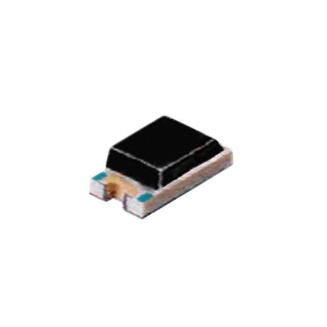
OP501DA(TT Electronics/Optek Technology)是一款NPN型硅光电晶体管,采用TO-18金属封装,带透明平顶透镜,具有高灵敏度、快速响应(典型上升/下降时间约15μs)和良好的可见光谱响应(峰值波长约850 nm,兼顾近红外)。其典型应用场景包括:

- 工业位置与限位检测:用于自动化产线中的物体有无检测、机械臂到位确认、传送带计数等,利用其抗电磁干扰能力强、无需物理接触的特点;
- 编码器与旋转检测:配合码盘或遮光片,实现电机转速测量、角度反馈及步进控制;
- 光隔离与信号耦合:在中低速数字隔离电路中作为接收端(如PLC输入模块、电源反馈回路),提供电气隔离(隔离电压达3000 Vrms);
- 消费电子与办公设备:应用于打印机纸张检测、复印机原稿定位、自动门感应等简单光控功能;
- 教育与原型开发:因结构坚固、驱动简单(仅需集电极接负载电阻+电源)、兼容TTL电平,常用于教学实验与嵌入式传感原型设计。

注意:该器件为模拟输出型光电晶体管,输出电流与光照强度近似线性,但非数字开关器件,实际应用中建议加施密特触发器或比较器以提升抗噪能力。不适用于高速通信或精密光强测量场景。
| 参数 | 数值 |
| 产品目录 | |
| 描述 | PHOTODARLINGTON NPN BLK 0805 SMD光电晶体管 Photo Darlington |
| 产品分类 | |
| 品牌 | TT Electronics/Optek Technology |
| 产品手册 | |
| 产品图片 |
|
| rohs | 符合RoHS无铅 / 符合限制有害物质指令(RoHS)规范要求 |
| 产品系列 | 光电晶体管,Optek / TT Electronics OP501DA- |
| 数据手册 | |
| 产品型号 | OP501DA |
| PCN过时产品 | |
| 上升时间 | 60 us |
| 下降时间 | 60 us |
| 产品目录页面 | |
| 产品种类 | 光电晶体管 |
| 其它名称 | 365-1480-2 |
| 功率-最大值 | 100mW |
| 商标 | Optek / TT Electronics |
| 安装类型 | 表面贴装 |
| 封装 | Reel |
| 封装/外壳 | 0805(2012 公制) |
| 封装/箱体 | SMD |
| 工厂包装数量 | 3000 |
| 最大功率耗散 | 100 mW |
| 最大工作温度 | + 85 C |
| 最大暗电流 | 100 nA |
| 最大集电极电流 | 32 mA |
| 最小工作温度 | - 25 C |
| 朝向 | 顶视图 |
| 标准包装 | 3,000 |
| 波长 | 935nm |
| 电压-集射极击穿(最大值) | 35V |
| 电流-暗(Id)(最大值) | 100nA |
| 电流-集电极(Ic)(最大值) | 32mA |
| 类型 | NPN Silicon Photo Darlington with Opaque Lens |
| 视角 | 150° |
| 集电极—发射极最大电压VCEO | 35 V |
| 集电极—射极击穿电压 | 35 V |
| 集电极—射极饱和电压 | 1 V |


- 商务部:美国ITC正式对集成电路等产品启动337调查
- 曝三星4nm工艺存在良率问题 高通将骁龙8 Gen1或转产台积电
- 太阳诱电将投资9.5亿元在常州建新厂生产MLCC 预计2023年完工
- 英特尔发布欧洲新工厂建设计划 深化IDM 2.0 战略
- 台积电先进制程称霸业界 有大客户加持明年业绩稳了
- 达到5530亿美元!SIA预计今年全球半导体销售额将创下新高
- 英特尔拟将自动驾驶子公司Mobileye上市 估值或超500亿美元
- 三星加码芯片和SET,合并消费电子和移动部门,撤换高东真等 CEO
- 三星电子宣布重大人事变动 还合并消费电子和移动部门
- 海关总署:前11个月进口集成电路产品价值2.52万亿元 增长14.8%


PDF Datasheet 数据手册内容提取
Silicon Phototransistor and Photo Darlington in Miniature 0805 SMD Package OP500, OP501, OP500DA, OP501DA OP501,DA Features: • High photo sensitivity • Fast response time • 0805 package size OP500,DA • Phototransistor or Photo Darlington Output • Choice of opaque or water clear flat lens Description: Each of these devices consists of a NPN silicon phototransistor mounted in a miniature SMT package with a 0805 size chip carrier that is compatible with most automated mounting and position sensing equipment. Both OP500, OP500DA and OP501, OP501DA have a flat lens. OP501 and OP501DA has an opaque lens that shields the device from stray light, whereas OP500 and OP500DA has a water clear lens. All devices have a wide viewing acceptance angle and higher collector current than devices without lenses especially on the OP500DA and OP501 which incorporate photo darlington die instead on the standard transistor. OP500, OP501, OP500DA and OP501DA are mechanically and spectrally matched to the OP200 series infrared LEDs. Applications: Ordering Information • Non-contact position sensing Part Number Sensor Viewing Angle Lead Length OP500 • Datum detection Phototransistor 150° OP501 • Machine automation OP500DA N/A Photo Darlington 150° • Optical encoders OP501DA OP500, OP501, OP500DA, OP501DA OP500 OP500DA OP501 OP501DA 1 1 SENSOR DICE 2 2 COLLECTOR Pin # Transistor 1 Collector 2 Emitter Recommended Solder Pad Patterns 2a RoHS Moisture OPTEK reserves the right to make changes at any time in order to improve design and to supply the best product possible. OPTEK Technology Inc. — 1645 Wallace Drive, Carrollton, Texas 75006 Issue A.4 02/09 Phone: (972) 323-2200 or (800) 341-4747 FAX: (972) 323-2396 sensors@optekinc.com www.optekinc.com Page 1 of 5
S ilicon Phototransistor and Photo Darlington in Miniature 0805 SMD Package OP500, OP501, OP500DA, OP501DA Absolute Maximum Ratings (T =25°C unless otherwise noted) A Storage Temperature Range -40o C to +100o C Operating Temperature Range -25o C to +85o C Lead Soldering Temperature(1) 260° C Collector-Emitter Voltage OP500, OP501 30 V OP500DA, OP501DA 35 V Emitter-Collector Voltage 5 V Collector Current OP500, OP501 20 mA OP500DA, OP501DA 32 mA Power Dissipation(2) OP500, OP501 75 mW OP500DA, OP501DA 100 mW Electrical Characteristics (T = 25°C unless otherwise noted) A SYMBOL PARAMETER MIN TYP MAX UNITS TEST CONDITIONS Input Diode On-State Collector Current I OP500, OP501 0.1 - - V = 5.0 V, E = 0.15 mW/cm2 (3) C(ON) mA CE E OP500DA, OP501DA 10.0 - - V = 5.0 V, E = 0.15 mW/cm2 (3) CE E Collector-Emitter Saturation Voltage V OP500, OP501 - - 0.3 I = 100 µA, E = 1.0 mW/cm2 (3) CE(SAT) V C E OP500DA, OP501DA - - 1.0 I = 1 mA, E = 0.15 mW/cm2 (3) C E I Collector-Emitter Dark Current - - 100 nA V = 5.0 V (4) CEO CC Collector-Emitter Breakdown Voltage 30 V OP500, OP501 - - V I = 100 µA, E = 0 BR(CEO) 35 C E OP500DA, OP501DA Emitter-Collector Breakdown Voltage V OP500, OP501 5 - - I = 100 µA, E = 0 BR(ECO) V E E OP500DA, OP501DA 5 - - I = 100 µA, E = 0 C E Rise and Fall Times OP500, OP501 15 - I = 1 mA, R = 1KΩ t t - µs C L r, f OP500DA, OP501DA 50 60 I = 1 mA, R = 1KΩ C L Notes: 1. Solder time less than 5 seconds at temperature extreme. 2. Derate linearly at 2.17 mW/° C above 25° C. 3. Light source is an unfiltered GaAs LED with a peak emission wavelength of 935 nm and a radiometric intensity level which varies less than 10% over the entire lens surface of the phototransistor being tested. 4. To calculate typical collector dark current in µA, use the formulate I = 10(0.04 t - ¾), where T is the ambient temperature in ° C. CEO A OPTEK reserves the right to make changes at any time in order to improve design and to supply the best product possible. Issue A.4 02/09 OPTEK Technology Inc. — 1645 Wallace Drive, Carrollton, Texas 75006 Page 2 of 5 Phone: (972) 323-2200 or (800) 341-4747 FAX: (972) 323-2396 sensors@optekinc.com www.optekinc.com
S ilicon Phototransistor and Photo Darlington in Miniature 0805 SMD Package OP500, OP501, OP500DA, OP501DA Relative Response vs. Wavelength 100% 80% e s n o 60% p s e R ative 40% OOPP550000,D A OOPP550011,D A el R 20% 0% 400 500 600 700 800 900 1000 1100 Wavelength (nm) OP500, OP501 Relative On-State Collector Current – Collector-Emitter Dark Current Ic (mA) vs. Temperature-T A vs. Collector-Emitter Voltage—V (V) CE 1000 2.00 Conditions: Ee = 0 mW/cm2 nA) VCE = 10V mA) 1.80 3 mW/cm2 ent ( 100 ent ( 1.60 2.5 mW/cm2 urr urr 1.40 C C Dark 10 ector 11..0200 2 mW/cm2 er oll 1.5 mW/cm2 mitt e C 0.80 E at or- St 0.60 1.0 mW/cm2 ct 1 n- e O 0.40 Coll - ON) 0.20 0.5 mW/cm2 C( 0 I -25 0 25 50 75 100 0 1 2 3 4 5 Temperature—(°C) Collector-Emitter Voltage (V) OPTEK reserves the right to make changes at any time in order to improve design and to supply the best product possible. OPTEK Technology Inc. — 1645 Wallace Drive, Carrollton, Texas 75006 Issue A.4 02/09 Phone: (972) 323-2200 or (800) 341-4747 FAX: (972) 323-2396 sensors@optekinc.com www.optekinc.com Page 3 of 5
S ilicon Phototransistor and Photo Darlington in Miniature 0805 SMD Package OP500, OP501, OP500DA, OP501DA OP500, OP501 Relative On-State Collector Current Relative On-State Collector Current-IC (mA) vs. Irradiance—Ee (mW/cm2) vs. Temperature-T A 160% 140% Normalized at Ee = 5mW/cm2 Normalized at TA = 25°C . Conditions: VCE = 5V, Conditions: VCE = 5V, 140% λ = 935nm, TA = 25 °C 130% λ = 935nm, TA = 25 °C nt urre 120% ent 120% or C 100% Curr 110% ct or olle 80% ect 100% e C Coll ativ 60% ve 90% Rel 40% elati 80% R 20% 70% 0 1.0 2.0 3.0 4.0 5.0 6.0 7.0 8.0 -25 0 25 50 75 100 Ee—Irradiance (mW/cm2) Temperature—(°C) OP500DA, OP501DA Relative On-State Collector Current – Collector-Emitter Dark Current Ic (mA) vs. Temperature-TA vs. Collector-Emitter Voltage—VCE (V) 30 1000 Conditions: Ee = 0 mW/cm2 1.2 mW/cm2 A) VCE = 10V mA) 25 n ( 1.0 mW/cm2 ent ( 100 rent 20 urr Cur 0.8 mW/cm2 k C or 17.5 ar ct er D 10 Colle 15.0 0.6 mW/cm2 ctor-Emitt 1 On-State 12.5 0.4 mW/cm2 Colle - ON) 10.0 0.2 mW/cm2 C( I 0 -25 0 25 50 75 100 0 0.5 1.0 1.5 2.5 3 Temperature—(°C) Collector-Emitter Voltage (V) OPTEK reserves the right to make changes at any time in order to improve design and to supply the best product possible. Issue A.4 02/09 OPTEK Technology Inc. — 1645 Wallace Drive, Carrollton, Texas 75006 Page 4 of 5 Phone: (972) 323-2200 or (800) 341-4747 FAX: (972) 323-2396 sensors@optekinc.com www.optekinc.com
Silicon Phototransistor and Photo Darlington in Miniature 0805 SMD Package OP500, OP501, OP500DA, OP501DA OP500DA, OP501DA Relative On-State Collector Current Relative On-State Collector Current-IC (mA) vs. Irradiance—Ee (mW/cm2) vs. Temperature-T A 140% Normalized at Ee = 1mW/cm2 Conditions: VCE = 5V, Normalized at TA = 25°C . % 160% λ = 935nm, TA = 25 °C 130% Conditions: VCE = 5V, — % nt 140% — 120% urre ent or C 120% Curr 110% ollect 100% ector 100% e C 80% Coll 90% ativ ve Rel 60% elati 80% R 40% 70% 0 0.50 1.0 1.5 2.0 -25 0 25 50 75 100 Irradiance- Ee(mW/cm2) Temperature—(°C) OPTEK reserves the right to make changes at any time in order to improve design and to supply the best product possible. OPTEK Technology Inc. — 1645 Wallace Drive, Carrollton, Texas 75006 Issue A.4 02/09 Phone: (972) 323-2200 or (800) 341-4747 FAX: (972) 323-2396 sensors@optekinc.com www.optekinc.com Page 5 of 5