ICGOO在线商城 > OP292GS

 Datasheet下载
- 型号: OP292GS
- 制造商: Analog
- 库位|库存: xxxx|xxxx
- 要求:
| 数量阶梯 | 香港交货 | 国内含税 |
| +xxxx | $xxxx | ¥xxxx |
查看当月历史价格
查看今年历史价格
OP292GS产品简介:
ICGOO电子元器件商城为您提供OP292GS由Analog设计生产,在icgoo商城现货销售,并且可以通过原厂、代理商等渠道进行代购。 提供OP292GS价格参考¥26.63-¥26.63以及AnalogOP292GS封装/规格参数等产品信息。 你可以下载OP292GS参考资料、Datasheet数据手册功能说明书, 资料中有OP292GS详细功能的应用电路图电压和使用方法及教程。
| 参数 | 数值 |
| -3db带宽 | - |
| 产品目录 | 集成电路 (IC) |
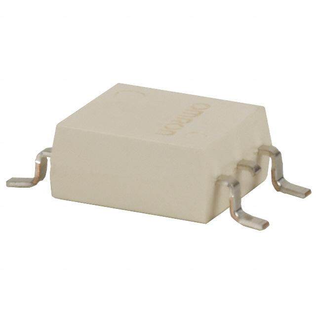
| 描述 | IC OPAMP GP 4MHZ 8SOIC |
| 产品分类 | Linear - Amplifiers - Instrumentation, OP Amps, Buffer Amps |
| 品牌 | Analog Devices Inc |
| 数据手册 | |
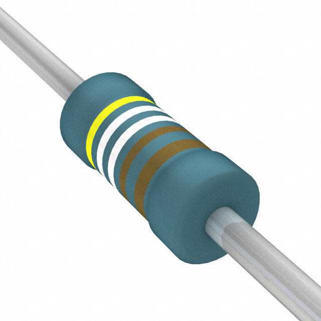
| 产品图片 |
|
| 产品型号 | OP292GS |
| rohs | 不符合限制有害物质指令(RoHS)规范要求 |
| 产品系列 | - |
| 产品培训模块 | http://www.digikey.cn/PTM/IndividualPTM.page?site=cn&lang=zhs&ptm=30008http://www.digikey.cn/PTM/IndividualPTM.page?site=cn&lang=zhs&ptm=26202 |
| 供应商器件封装 | 8-SOIC |
| 包装 | 管件 |
| 压摆率 | 4 V/µs |
| 增益带宽积 | 4MHz |
| 安装类型 | 表面贴装 |
| 封装/外壳 | 8-SOIC(0.154",3.90mm 宽) |
| 工作温度 | -40°C ~ 125°C |
| 放大器类型 | 通用 |
| 标准包装 | 98 |
| 电压-电源,单/双 (±) | 4.5 V ~ 33 V, ±2.25 V ~ 16.5 V |
| 电压-输入失调 | 1mV |
| 电流-电源 | 1mA |
| 电流-输入偏置 | 375nA |
| 电流-输出/通道 | 10.5mA |
| 电路数 | 2 |
| 视频文件 | http://www.digikey.cn/classic/video.aspx?PlayerID=1364138032001&width=640&height=505&videoID=2245193153001http://www.digikey.cn/classic/video.aspx?PlayerID=1364138032001&width=640&height=505&videoID=2245193159001 |
| 输出类型 | - |


- 商务部:美国ITC正式对集成电路等产品启动337调查
- 曝三星4nm工艺存在良率问题 高通将骁龙8 Gen1或转产台积电
- 太阳诱电将投资9.5亿元在常州建新厂生产MLCC 预计2023年完工
- 英特尔发布欧洲新工厂建设计划 深化IDM 2.0 战略
- 台积电先进制程称霸业界 有大客户加持明年业绩稳了
- 达到5530亿美元!SIA预计今年全球半导体销售额将创下新高
- 英特尔拟将自动驾驶子公司Mobileye上市 估值或超500亿美元
- 三星加码芯片和SET,合并消费电子和移动部门,撤换高东真等 CEO
- 三星电子宣布重大人事变动 还合并消费电子和移动部门
- 海关总署:前11个月进口集成电路产品价值2.52万亿元 增长14.8%


PDF Datasheet 数据手册内容提取
Dual/Quad Single-Supply Operational Amplifiers Data Sheet OP292/OP492 FEATURES PIN CONFIGURATIONS Single-supply operation: 4.5 V to 33 V OUTA 1 8 +V Input common-mode includes ground –INA 2 OP292 7 OUTB Output swings to ground +INA 3 TOP VIEW 6 –INB HHiigghh sglaeiwn braatned: 3w Vid/tμhs: 4 MHz –V 4 (Not to Scale) 5 +INB 00310-00 Figure 1. 8-Lead Narrow-Body SOIC (S-Suffix) Low input offset voltage High open-loop gain No phase inversion OUTA 1 14 OUTD APPLICATIONS –INA 2 13 –IND Disk drives +INA 3 OP492 12 +IND +V 4 TOP VIEW 11 –V Mobile phones (Not to Scale) +INB 5 10 +INC Servo controls MPaogdeerms s and fax machines O–UINTBB 67 98 –OIUNTCC 00310-002 Figure 2. 14-Lead Narrow-Body SOIC (S-Suffix) Power supply monitors and controls Battery-operated instrumentation GENERAL DESCRIPTION The OP292/OP492 are low cost, general-purpose dual and quad The OP292/OP492 series is unity-gain stable and features an operational amplifiers designed for single-supply applications outstanding combination of speed and performance for single- and are ideal for 5 V systems. or dual-supply operation. The OP292/OP492 provide a high slew rate, high bandwidth, with open-loop gain exceeding Fabricated on Analog Devices, Inc., CBCMOS process, the 40,000 and offset voltage under 0.8 mV (OP292) and 1 mV OP292/OP492 series has a PNP input stage that allows the input (OP492). With these combinations of features and low supply voltage range to include ground. A BiCMOS output stage enables current, the OP292/OP492 series is an excellent choice for the output to swing to ground while sinking current. battery-operated applications. The OP292/OP492 series performance is specified for single- or dual-supply voltage operation over the extended industrial temperature range (−40°C to +125°C). Rev. D Document Feedback Information furnished by Analog Devices is believed to be accurate and reliable. However, no responsibility is assumed by Analog Devices for its use, nor for any infringements of patents or other One Technology Way, P.O. Box 9106, Norwood, MA 02062-9106, U.S.A. rights of third parties that may result from its use. Specifications subject to change without notice. No license is granted by implication or otherwise under any patent or patent rights of Analog Devices. Tel: 781.329.4700 ©1993–2015 Analog Devices, Inc. All rights reserved. Trademarks and registered trademarks are the property of their respective owners. Technical Support www.analog.com
OP292/OP492 Data Sheet TABLE OF CONTENTS Features .............................................................................................. 1 Typical Applications ....................................................................... 14 Applications ....................................................................................... 1 Direct Access Arrangement for Telephone Line Interface ... 14 Pin Configurations ........................................................................... 1 Single-Supply Instrumentation Amplifier .............................. 14 General Description ......................................................................... 1 DAC Output Amplifier .............................................................. 14 Revision History ............................................................................... 2 50 Hz/60 Hz Single-Supply Notch Filter ................................. 15 Specifications ..................................................................................... 3 Four-Pole Bessel Low-Pass Filter ............................................. 15 Electrical Characteristics ............................................................. 3 Low Cost, Linearized Thermistor Amplifier .............................. 15 Absolute Maximum Ratings ............................................................ 6 Single-Supply Ultrasonic Clamping/Limiting Receiver Thermal Resistance ...................................................................... 6 Amplifier ..................................................................................... 16 ESD Caution .................................................................................. 6 Precision Single-Supply Voltage Comparator ........................ 16 Typical Performance Characteristics ............................................. 7 Programmable Precision Window Comparator .................... 16 Applications Information .............................................................. 13 Outline Dimensions ....................................................................... 17 Phase Reversal ............................................................................. 13 Ordering Guide .......................................................................... 17 Power Supply Considerations ................................................... 13 REVISION HISTORY 8/15—Rev. C to Rev. D Changes to Figure 39 and Figure 41............................................. 15 Change to General Description Section ........................................ 1 Deleted OP492 SPICE Macro-Model Section ............................ 16 Changes to Ordering Guide .......................................................... 17 Changes to Figure 44 ...................................................................... 16 Updated Outline Dimensions ....................................................... 17 5/09—Rev. B to Rev. C Changes to Ordering Guide .......................................................... 17 Deleted 8-Lead PDIP and 14-Lead PDIP ........................ Universal Changes to Features Section and General Description Section . 1 10/02—Rev. A to Rev. B Changed V = 5 V to V = ±15 V .................................................... 4 Edits to Outline Dimensions ......................................................... 18 S S Changes to Table 3 and Table 4 ....................................................... 6 Changes to Figure 21 Caption and Figure 24 Caption .............. 10 1/02—Rev. 0 to Rev. A Changes to Figure 29 ...................................................................... 11 Deleted Wafer Test Limits ................................................................ 4 Changes to Figure 35 ...................................................................... 13 Deleted Dice Characteristics ............................................................ 4 Deleted OP292 SPICE Macro-Model Section ............................ 14 Edits to Ordering Guide ................................................................ 20 Changes to Figure 38 ...................................................................... 14 Rev. D | Page 2 of 20
Data Sheet OP292/OP492 SPECIFICATIONS ELECTRICAL CHARACTERISTICS V = 5 V, V = 0 V, V = 2 V, T = 25°C, unless otherwise noted. S CM O A Table 1. Parameter Symbol Conditions Min Typ Max Unit INPUT CHARACTERISTICS Offset Voltage OP292 V 0.1 0.8 mV OS −40°C ≤ T ≤ +85°C 0.3 1.2 mV A −40°C ≤ T ≤ +125°C 0.5 2.5 mV A OP492 V 0.1 1 mV OS −40°C ≤ T ≤ +85°C 0.3 1.5 mV A −40°C ≤ T ≤ +125°C 0.5 2.5 mV A Input Bias Current I 450 700 nA B −40°C ≤ T ≤ +85°C 0.75 2.5 µA A −40°C ≤ T ≤ +125°C 3.0 5.0 µA A Input Offset Current I 7 50 nA OS −40°C ≤ T ≤ +85°C 100 700 nA A −40°C ≤ T ≤ +125°C 0.4 1.2 µA A Input Voltage Range 0 4.0 V Common-Mode Rejection Ratio CMRR V = 0 V to 4.0 V 75 95 dB CM −40°C ≤ T ≤ +85°C 70 93 dB A −40°C ≤ T ≤ +125°C 65 90 dB A Large Signal Voltage Gain A R = 10 kΩ, V = 0.1 V to 4 V 25 200 V/mV VO L O −40°C ≤ T ≤ +85°C 10 100 V/mV A −40°C ≤ T ≤ +125°C 5 50 V/mV A Offset Voltage Drift ΔV /ΔT −40°C ≤ T ≤ +125°C 2 10 µV/°C OS A Long-Term V Drift1 ΔV /ΔT 1 µV/Month OS OS Bias Current Drift ΔI /ΔT −40°C ≤ T ≤ +85°C 6 pA/°C B A −40°C ≤ T ≤ +125°C 400 pA/°C A Offset Current Drift ΔI /ΔT −40°C ≤ T ≤ +85°C 1.5 pA/°C OS A −40°C ≤ T ≤ +125°C 2 pA/°C A OUTPUT CHARACTERISTICS Output Voltage Swing High V R = 100 kΩ to GND OUT L −40°C ≤ T ≤ +125°C 4.0 4.3 V A R = 2 kΩ to GND 3.8 4.1 V L −40°C ≤ T ≤ +125°C 3.7 3.9 V A Low V R = 100 kΩ to V+ 8 20 mV OUT L −40°C ≤ T ≤ +125°C 12 20 mV A R = 2 kΩ to V+ 280 450 mV L −40°C ≤ T ≤ +125°C 300 550 mV A Short-Circuit Current Limit I 5 8 mA SC POWER SUPPLY Power Supply Rejection Ratio PSRR V = 4.5 V to 30 V, V = 2 V 75 95 dB S O −40°C ≤ T ≤ +125°C 70 90 dB A Supply Current Per Amp I V = 2 V 0.8 1.2 mA SY O Rev. D | Page 3 of 20
OP292/OP492 Data Sheet Parameter Symbol Conditions Min Typ Max Unit DYNAMIC PERFORMANCE Slew Rate SR R = 10 kΩ 3 V/µs L −40°C ≤ T ≤ +125°C 1 2 V/µs A Gain Bandwidth Product GBP 4 MHz Phase Margin φ 75 Degrees m Channel Separation CS f = 1 kHz 100 dB O NOISE PERFORMANCE Voltage Noise e p-p 0.1 Hz to 10 Hz 25 µV p-p n Voltage Noise Density e f = 1 kHz 15 nV/√Hz n Current Noise Density i 0.7 pA/√Hz n 1 Long-term offset voltage drift is guaranteed by 1,000 hours life test performed on three independent wafer lots at 125°C with LTPD of 1.3. Rev. D | Page 4 of 20
Data Sheet OP292/OP492 V =±15 V, V = 0 V, V = 2 V, T = 25°C, unless otherwise noted. S CM O A Table 2. Parameter Symbol Conditions Min Typ Max Unit INPUT CHARACTERISTICS Offset Voltage OP292 V 1.0 2.0 mV OS −40°C ≤ T ≤ +85°C 1.2 2.5 mV A −40°C ≤ T ≤ +125°C 1.5 3 mV A OP492 V 1.4 2.5 mV OS −40°C ≤ T ≤ +85°C 1.7 2.8 mV A −40°C ≤ T ≤ +125°C 2 3 mV A Input Bias Current I 375 700 nA B −40°C ≤ T ≤ +125°C 0.5 1 µA A Input Offset Current I 7 50 nA OS −40°C ≤ T ≤ +85°C 20 100 nA A −40°C ≤ T ≤ +125°C 0.4 1.2 µA A Input Voltage Range1 −11 +11 V Common-Mode Rejection Ratio CMRR V = ±11 V 78 100 dB CM −40°C ≤ T ≤ +125°C 75 95 dB A Large Signal Voltage Gain A R = 10 kΩ, V =±10 V 25 120 V/mV VO L O −40°C ≤ T ≤ +85°C 10 75 V/mV A −40°C ≤ T ≤ +125°C 5 60 V/mV A Offset Voltage Drift ΔV /ΔT −40°C ≤ T ≤ +125°C 4 10 µV/°C OS A Bias Current Drift ΔI /ΔT −40°C ≤ T ≤ +125°C 3 pA/°C B A OUTPUT CHARACTERISTICS Output Voltage Swing V R = 2 kΩ to GND ±11 ±12.2 V O L −40°C ≤ T ≤ +125°C ±10 ±11 V A R = 100 kΩ to GND ±13.8 ±14.3 V L −40°C ≤ T ≤ +125°C ±13.5 ±14.0 mV A Short-Circuit Current Limit I Short circuit to GND 8 10.5 mA SC POWER SUPPLY Power Supply Rejection Ratio PSRR V = ±2.25 V to ±15 V 75 86 dB S −40°C ≤ T ≤ +125°C 70 83 dB A Supply Current Per Amp I V = 0 V 1 1.4 mA SY O DYNAMIC PERFORMANCE Slew Rate SR R =10 kΩ 2.5 4 V/µs L −40°C ≤ T ≤ +125°C 2 3 V/µs A Gain Bandwidth Product GBP 4 MHz Phase Margin φ 75 Degrees m Channel Separation CS f = 1 kHz 100 dB O NOISE PERFORMANCE Voltage Noise e p-p 0.1 Hz to 10 Hz 25 µV p-p n Voltage Noise Density e f = 1 kHz 15 nV/√Hz n Current Noise Density i 0.7 pA/√Hz n 1 Input voltage range is guaranteed by CMRR tests. Rev. D | Page 5 of 20
OP292/OP492 Data Sheet ABSOLUTE MAXIMUM RATINGS THERMAL RESISTANCE Table 3. θ is specified for the worst-case conditions, that is, a device Parameter Rating JA soldered in the circuit board for the surface-mount packages. Supply Voltage 33 V Input Voltage Range1 −15 V to +14 V Table 4. Thermal Resistance Differential Input Voltage1 V1 Package Type θ θ Unit JA JC Output Short-Circuit Duration Unlimited 8-Lead SOIC 158 43 °C/W Storage Temperature Range −65°C to +150°C 14-Lead SOIC 120 36 °C/W Operating Temperature Range −40°C to +125°C Junction Temperature Range −65°C to +125°C Lead Temperature Range (Soldering, 60 sec) 300°C ESD CAUTION 1 For supply voltages less than 36 V, the absolute maximum input voltage is equal to the supply voltage. Stresses at or above those listed under Absolute Maximum Ratings may cause permanent damage to the product. This is a stress rating only; functional operation of the product at these or any other conditions above those indicated in the operational section of this specification is not implied. Operation beyond the maximum operating conditions for extended periods may affect product reliability. Rev. D | Page 6 of 20
Data Sheet OP292/OP492 TYPICAL PERFORMANCE CHARACTERISTICS 200 160 VS = 5V 175 VCM = 0V 140 VS = 5V TA= 25°C VCM = 0V 720 OP AMPS TA = 25°C 150 120 600 OP AMPS 125 100 UNITS100 UNITS 80 75 60 50 40 205–500 –400 –300INP–2U0T0 O–F1F0S0ET V0OLTA1G00E, VO20S0(µV)300 400 50000310-003 2–000.5 –0.4 –0.3IN–P0.U2T O–0F.1FSET0 VOL0T.1AGE0,. 2VOS0(.m3V)0.4 0.5 0.600310-006 Figure 3. OP292 Input Offset Voltage Distribution @ 5 V Figure 6. OP492 Input Offset Voltage Distribution @ 5 V 320 240 280 7VVT2ASC0 M== O =2±P 510 °5AVCVMPS 200 VVTASC M== =2± 510°5VCV 240 600 OP AMPS 160 200 UNITS160 UNITS 120 120 80 80 40 400 00310-004 0 0 0.2 0.4INPU0T.6 OFF0S.8ET V1O.0LTA1G.2E, VO1S.4(mV)1.6 1.8 2.0 0 0.2 0.4INPU0T.6 OFF0S.8ET V1O.0LTA1G.2E, VO1S.4(mV)1.6 1.8 2.0 00310-007 Figure 4. OP292 Input Offset Voltage Distribution @ ±15 V Figure 7. OP492 Input Offset Voltage Distribution @ ±15 V 160 160 140 6VV–04SC00 M= °O C =5P V≤0 AVTMAP≤S +125°C 140 VV–4SC0 M=° C =5 V≤0 VTA≤ +125°C 120 120 600 OP AMPS 100 100 NITS 80 NITS 80 U U 60 60 40 40 200 00310-005 200 0 0.4 0.8 1.2 1T.C6VOS2.(0µV/°C2.)4 2.8 3.2 3.6 4.0 0 0.5 1.0 1.5 T2C.0VOS2(.µ5V/°C3).0 3.5 4.0 4.5 5.0 00310-008 Figure 5. OP292 Temperature Drift (TCVOS) Distribution @ 5 V Figure 8. OP492 Temperature Drift (TCVOS) Distribution @ 5 V Rev. D | Page 7 of 20
OP292/OP492 Data Sheet 240 200 210 VV–4SC0 M=° C =5 V≤0 VTA≤ +125°C 175 6VV–04SC00 M= °O C =±P 1≤0 5 AVTVMAP≤S +125°C 180 600 OP AMPS 150 150 125 S S NIT120 NIT100 U U 90 75 60 50 30 25 00 1 2 3TCVOS4(µV/°C)5 6 7 8 00310-009 00 1 2 3TCVOS4(µV/°C)5 6 7 8 00310-012 Figure 9. OP292 Temperature Drift (TCVOS) Distribution @ ±15 V Figure 12. OP492 Temperature Drift (TCVOS) Distribution @ ±15 V 600 900 500 VVSO == 54VV 800 RL = 10kΩ VVSO == 54VV 700 V) V) m m V/400 V/ 600 N ( N ( AI AI 500 G G P 300 P O O 400 O O EN-L200 RL= 10kΩ EN-L 300 OP OP RL= 2kΩ 200 100 RL= 2kΩ 100 0–50 –25 0 TEMP2E5RATUR5E0 (°C) 75 100 125 00310-010 0–50 –25 0 TEM2P5ERATUR5E0 (°C) 75 100 125 00310-013 Figure 10. OP292 Open-Loop Gain vs. Temperature @ 5 V Figure 13. OP492 Open-Loop Gain vs. Temperature @ 5 V 250 400 VS = ±15V VS = ±15V VO = ±10V 350 VO = ±10V 200 mV) mV) 300 RL = 10kΩ OPEN-LOOP GAIN (V/110500 RL= 2kΩRL= 10kΩ OPEN-LOOP GAIN (V/ 112205050000 RL= 2kΩ 50 50 0–50 –25 0 TEMP2E5RATUR5E0 (°C) 75 100 125 00310-011 0–50 –25 0 TEM2P5ERATUR5E0 (°C) 75 100 125 00310-014 Figure 11. OP292 Open-Loop Gain vs. Temperature @ ±15 V Figure 14. OP492 Open-Loop Gain vs. Temperature @ ±15 V Rev. D | Page 8 of 20
Data Sheet OP292/OP492 1.4 1.4 A) A) ER (m 1.2 VS = ±15V ER (m 1.2 FI FI PLI 1.0 PLI 1.0 VS = ±15V M M A A R R PE 0.8 VS = +5V PE 0.8 T T N N E E R R R 0.6 R 0.6 VS = +5V U U C C Y Y L L PP 0.4 PP 0.4 U U S S 0.2 0.2 –50 –25 0 TEM2P5ERATUR5E0 (°C) 75 100 125 00310-015 –50 –25 0 TEM2P5ERATUR5E0 (°C) 75 100 125 00310-018 Figure 15. OP292 Supply Current per Amplifier vs. Temperature Figure 18. OP492 Supply Current per Amplifier vs. Temperature 6 6 VS = ±15V +SR VS = ±15V VO = ±10V VO = ±10V 5 5 +SR V/µs) 4 –SR V/µs) 4 –SR RATE ( 3 +SR RATE ( 3 +SR W W E E SL 2 SL 2 –SR –SR 1 1 VS = 5V VS = 5V VO = 0.1V, 4V VO = 0.1V, 4V 0 0 –50 –25 0 TEM2P5ERATUR5E0 (°C) 75 100 125 00310-016 –50 –25 0 TEM2P5ERATUR5E0 (°C) 75 100 125 00310-019 Figure 16. OP292 Slew Rate vs. Temperature Figure 19. OP492 Slew Rate vs. Temperature 90 90 80 TA = 25°C 80 TA = 25°C V+ = 5V VS = 10kΩ 70 VR–L == 01V0kΩ 70 RL = 10kΩ 60 60 GAIN GAIN B) 50 B) 50 d d N ( 40 N ( 40 GAI 30 PMHAARSGEIN 135 GAI 30 PMHAARSGEIN +135 S) 20 PHASE = 83° 90 ees) 20 PHASE = 92° +90 REE 10 45 Degr 10 +45 DEG E ( E ( 0 0 AS 0 0 AS H H P P –101k 10k FREQU1E0N0CkY (Hz) 1M 10M–45 00310-017 –101k 10k FREQU1E0N0CkY (Hz) 1M 10M–45 00310-020 Figure 17. OP292/OP492 Open-Loop Gain and Phase vs. Frequency @ 5 V Figure 20. OP292/OP492 Open-Loop Gain and Phase vs. Frequency @ ±15 V Rev. D | Page 9 of 20
OP292/OP492 Data Sheet 50 50 TA = 25°C 40 V+ = 5V 40 TA = 25°C V– = 0V VS = ±15V B) B) d d N ( 30 N ( 30 AI AI G G P P O 20 O 20 O O L L D- D- E E OS 10 OS 10 L L C C 0 0 –101k 10k FREQU1E0N0CkY (Hz) 1M 10M 00310-021 –101k 10k FREQU1E0N0CkY (Hz) 1M 10M 00310-024 Figure 21. OP292/OP492 Closed-Loop Gain vs. Frequency @ 5 V Figure 24. OP292/OP492 Closed-Loop Gain vs. Frequency @ ±15 V 120 120 TA = 25°C TA = 25°C V+ = 5V B)100 V– = 0V B)100 VS = ±15V d d N ( N ( O O TI 80 TI 80 C C E E J J E E E R 60 E R 60 D D O O M M N- 40 N- 40 O O M M M M O O C 20 C 20 0100 1k FREQUE10NkCY (Hz) 100k 1M 00310-022 0100 1k FREQUE10NkCY (Hz) 100k 1M 00310-025 Figure 22. OP292/OP492 CMR vs. Frequency @ 5 V Figure 25. OP292/OP492 CMR vs. Frequency @ ±15 V 120 120 TA = 25°C TA = 25°C dB)100 VS = 5V dB)100 VS = ±15V N ( N ( O O TI 80 TI 80 C C E E J J RE RE +PSSR Y 60 Y 60 L L P P P P U U –PSSR R S 40 R S 40 E E W W O O P 20 P 20 0 0 100 1k FREQUE10NkCY (Hz) 100k 1M 00310-023 100 1k FREQUE10NkCY (Hz) 100k 1M 00310-026 Figure 23. OP292/OP492 PSR vs. Frequency @ 5 V Figure 26. OP292/OP492 PSR vs. Frequency @ ±15 V Rev. D | Page 10 of 20
Data Sheet OP292/OP492 4.8 15.0 VS = ±15V RL = 100kΩ VS = 5V V) 14.0 WING (V) 4.6 RL= 100kΩ T SWING ( 13.0 RRLL == 21k0ΩkΩ GE S 4.4 UTPU 12.0 TA O 11.0 OL RL= 10kΩ V 4.2 T V) 10.0 PU G ( OUT 4.0 RL= 2kΩ SWIN–14.0 RL = 2kΩ PUT –14.5 RL = 100kΩ RL = 10kΩ T U 3.8–50 –25 0 TEM2P5ERATUR5E0 (°C) 75 100 125 00310-027 –O–15.0–50 –25 0 TEM2P5ERATUR5E0 (°C) 75 100 12500310-030 Figure 27. OP292/OP492 VOUT Swing vs. Temperature @ 5 V Figure 30. OP292/OP492 VOUT Swing vs. Temperature @ ±15 V 10 600 VS = 5V VS = ±15V VCM = 0V VCM = 0V 500 A) A) T (µ T (n 400 N N RE RE OP492 CUR 1 OP492 CUR 300 S S OP292 A A UT BI OP292 UT BI 200 P P N N I I 100 0.1–50 –25 0 TEM2P5ERATUR5E0 (°C) 75 100 125 00310-028 0–50 –25 0 TEM2P5ERATUR5E0 (°C) 75 100 125 00310-031 Figure 28. OP292/OP492 Input Bias Current vs. Temperature @ 5 V Figure 31. OP292/OP492 Input Bias Current vs. Temperature @ ±15 V –40 0.50 0.48 0.46 –60 –RAIL 0.44 dB) 0.42 +15V ON ( –80 RVSL == +2k5ΩV, ±15V A) 0.40 ANNEL SEPARATI–1–0900 VO = 3V p-p I CURRENT (nB000000......333323408286 VA IN–15V CH 0.26 –110 0.24 +RAIL 0.22 0.20 –120 0.18 0 10 F1R0E0QUENCY (H1kz) 10k 100k 00310-029 0 1 2 3 4 5 6 V7IN (V8) 9 10 11 12 13 14 15 00310-032 Figure 29. OP292/OP492 Channel Separation Figure 32. OP292/OP492 IB Current vs. Common-Mode Voltage Rev. D | Page 11 of 20
OP292/OP492 Data Sheet CHM AK R80:0 0H1d0zV00 FHSz 100dV/DIV BW2:5 k1H50zHMzKR: 16.9µV/Hz 00310-033 Figure 33. Voltage Noise Density Rev. D | Page 12 of 20
Data Sheet OP292/OP492 APPLICATIONS INFORMATION PHASE REVERSAL 1V/DIV The OP492 has built-in protection against phase reversal when the input voltage goes to either supply rail. In fact, it is safe for 5V the input to exceed either supply rail by up to 0.6 V with no risk 0V of phase reversal. However, the input should not go beyond the 10V p-p OP492 positive supply rail by more than 0.9 V; otherwise, the output will reverse phase. If this condition occurs, the problem can be ftihxee din bpyu ta dpidnin. Wg ait 5h kthΩis c audrdreitnito lnim, thitein ign preusti sctaonr gino stoer mieso rwei tthh an 2kΩ 4ms/DIV 00310-035 5 V beyond the positive rail without phase reversal. Figure 35. No Negative Rail Phase Reversal, Even with Input Signal at 5 V Below Ground An input voltage that is as much as 5 V below the negative rail will not result in phase reversal. POWER SUPPLY CONSIDERATIONS The OP292/OP492 are designed to operate equally well at single 1V +5 V or ±15 V supplies. The lowest supply voltage recommended 100 5V 90 is 4.5 V. It is a good design practice to bypass the supply pins with a 0V 11.8V p-p OP492 0.1 µF ceramic capacitor. It helps improve filtering of high 2kΩ frequency noise. 10 For dual-supply operation, the negative supply (V−) must be 0% 5µs 00310-034 aopr pinlie tdh ea tc tahsee soafm ae l otisms eo, fo trh bee Vfo−re s Vup+p. lIyf ,V w+h iisle a peiptlhieedr ibnepfourte i Vs −, Figure 34. Output Phase Reverse If Input Exceeds connected to ground or another low impedance source, excessive the Positive Supply (V+) by More Than 0.9 V input current may result. Potentially damaging levels of input current can destroy the amplifier. If this condition can exist, simply add a l kΩ or larger resistor in series with the input to eliminate the problem. Rev. D | Page 13 of 20
OP292/OP492 Data Sheet TYPICAL APPLICATIONS 5V DIRECT ACCESS ARRANGEMENT FOR TELEPHONE LINE INTERFACE 5 8 VIN OP1/2292 7 VOUT Figure 36 shows a 5 V single-supply transmit/receive telephone line 1/2 1 4 interface for a modem circuit. It allows full duplex transmission OP292 of modem signals on a transformer-coupled 600 V line in a differential manner. The transmit section gain can be set for the VREF 20kΩ 5kΩ 5kΩ 20kΩ sgpaeinc icfiacn m boe daepmpr odpevriiactee olyu stepluetc.t Sedim bialasreldy ,o tnh et hreec meioved eamm pdleifviiecre RG VOUT = 5 +40RkGΩ +VREF 00310-037 input requirements. The circuit operates on a single 5 V supply. Figure 37. Single-Supply Instrumentation Amplifier The standard value resistors allow the use of a SIP-packaged In this configuration, the output can swing to near 0 V; however, resistor array; coupled with a quad op amp in a single package, be careful because the common-mode voltage range of the input this offers a compact, low part count solution. cannot operate to 0 V. This is because of the limitation of the TX GAIN ADJUST circuit configuration where the first amplifier must be able to 50kΩ TO TELEPHONE swing below ground to attain a 0 V common-mode voltage, LINE 20kΩ 0.1µF which it cannot do. Depending on the gain of the instrumentation TRANSMIT 1:1 300kΩ 1/4 TXA amplifier, the input common-mode extends to within about 0.3 V OP492 300kΩ of zero. The worst-case common-mode limit for a given gain 20kΩ can be easily calculated. T1 20kΩ DAC OUTPUT AMPLIFIER 6.2V 6.2V The OP292/OP492 are ideal for buffering the output of single- 1/4 OP492 supply digital-to-analog converters (DACs). Figure 38 shows a 5V DC typical amplifier used to buffer the output of a CMOS DAC MODEM 5kΩ that is connected for single-supply operation. To do that, the normally current output 12-bit CMOS DAC (R-2R ladder 100pF 5kΩ 10µF type) is connected backward to produce a voltage output. This operating configuration necessitates a low voltage reference. In 20kΩ this case, a 1.235 V low power reference is used. The relatively 5V high output impedance (10 kΩ) is buffered by the OP292, and 0.1µF RX GAIN ADJUST 20kΩ at the same time, gained up to a much more usable level. The 20kΩ 50kΩ 0.1µF 1/4 RECEIVE potentiometer provides an accurate gain trim for a 4.095 V full- 20kΩ OP492 RXA scale, allowing 1 mV increment per LSB of control resolution. 20kΩ 00310-036 Ta hcoe sDt-AeCffe8c0t4i3ve d, ecvoimcep caocmt esos liunt aionn 8 t-ole aad 1 P2-DbIiPt apnaaclkoagg ec,h parnonveidl.i ng Figure 36. Universal Direct Access Arrangement for Telephone Line Interface 5V SINGLE-SUPPLY INSTRUMENTATION AMPLIFIER 1/2 A low cost, single-supply instrumentation amplifier can be built 5V OP292 VOUT 5V DAC8043 1mV/LSB as shown in Figure 37. The circuit uses two op amps to form a 1 VREF VVDDDD 8 0V – 4.095V high input impedance differential amplifier. Gain can be set by 7.5kΩ FS NC 2 RFB CLCKlk 7 20kΩ selecting resistor R , which can be calculated using the transfer G 1.235V function equation. Normally, V is set to 0 V. Then the output 3 IOUT SSRrIi 6 REF AD589 8.45kΩ voltage is a function of the gain times the differential input voltage. 4 GND LD 5 However, the output can be offset by setting V from 0 V to 500kΩ REF 4 V, as long as the input common-mode voltage of the amplifier is not exceeded. LDSRI CLK CDOINGTITRAOLL 00310-038 Figure 38. 12-Bit Single-Supply DAC with Serial Bus Control Rev. D | Page 14 of 20
Data Sheet OP292/OP492 50 Hz/60 Hz SINGLE-SUPPLY NOTCH FILTER 5V 5V 6 F60ig Hurze r3e9je schtioowns w ah niloet cpho wfiletreerd t hbayt oanchlyi eav seisn ngelea r1l2y V30 s duBpp olfy . 5kΩ 0.01µF2 1/2 8 1 0.022µF5OP1/2292 7 VOUT The circuit also works well on 5 V systems. The filter uses a VIN 3OP292 4 1.1kΩ 14.3kΩ twin-T configuration, whose frequency selectivity depends 100µF 1.78kΩ 16.2kΩ 2200pF htheea vtwiliyn o-Tn sthecet rioelna.t iMvey mlaart icsh ain ggo oofd t hceh coaicpea cfiotro rtsh aen cda preasciisttoorrss oinf 5kΩ 3300pF 00310-040 the twin-T, and the relative matching of the capacitors and resistors Figure 40. Four-Pole Bessel Low-Pass Filter Using Sallen-Key Topology determines the pass-band symmetry of the filter. Using 1% LOW COST, LINEARIZED THERMISTOR AMPLIFIER resistors and 5% capacitors produces satisfactory results. An inexpensive thermometer amplifier circuit can be implemented The amount of rejection and the Q of the filter is solely determined using low cost thermistors. One such implementation is shown by one resistor and is shown in the table with Figure 39. The in Figure 41. The circuit measures temperature over the range bottom amplifier is used to split the supply to bias the amplifier of 0°C to 70°C to an accuracy of ±0.3°C as the linearization to midlevel. The circuit can be modified to reject 50 Hz by simply circuit works well within a narrow temperature range. However, it changing the resistors in the twin-T section (R1 through R4) can measure higher temperatures but at a slightly reduced accuracy. from 2.67 kΩ to 3.16 kΩ and by changing R5 to ½ of 3.16 kΩ. For To achieve the aforementioned accuracy, the nonlinearity of the best results, the common value resistors can be from a resistor thermistor must be corrected. This is done by connecting the array for optimum matching characteristics. thermistor in parallel with the 10 kΩ in the feedback loop of the R2 first stage amplifier. A constant operating current of 281 µA is 2.67kΩ supplied by the resistor R1 with the 5 V reference from the 2.67kRΩ1 C1 C2 12V REF195 such that the self-heating error of the thermistor is 1/4 1µF 1µF kept below 0.1°C. OP492 1/4 VIN OP492 VOUT In many cases, the thermistor is placed some distance from the R3 R4 signal conditioning circuit. Under this condition, a 0.1 µF capacitor 2.67kΩ 2.67kΩ R6 placed across R2 will help to suppress noise pickup. 100kΩ C3 R5 (1µF2 ×µ F2) 1(2.3.6375kk Ω÷ 2) R1k7Ω R8kQΩ This linearization network creates an offset voltage that is corrected by summing a compensating current with Potentiometer P1. The 12V temperature dependent signal is amplified by the second stage, R8 1/4 6V 100kΩ OP492 producing a transfer coefficient of −10 mV/°C at the output. R9 +C4 To calibrate, a precision decade box can be used in place of the 100kΩ 1µF thermistor. For 0°C trim, the decade box is set to 32.650 kΩ, and P1 is adjusted until the output of the circuit reads 0 V. To FILTER Q RQ (kΩ) REJECTION (dB) VOLTAGE GAIN trim the circuit at the full-scale temperature of 70°C, the decade 0.75 1.0 40 1.33 box is then set to 1.752 kΩ, and P2 is adjusted until the circuit 1.00 2.0 35 1.50 reads −0.70 V. 1.25 3.0 30 1.60 2.50 8.0 25 1.80 RT1 5.00 18 20 1.90 15V 10kΩ NTC 10.00 38 15 1.95 R12 N1 . O FATONERDS 5R05H TzO A 1PF.Pi5gL8ukICrΩeA (T33I9.O1.6 NSk iΩCn Hg÷A l2eN)-SGuEp Rp1l2y T5O0 HR4z /T6O0 3H.1z6 NkΩotch Filter 00310-039 1.0µF REF1915µF 17.8kΩ 117/R2.81k2Ω 10Rk3Ω 7.8R76kΩP270020°CΩTRIM OP292 5V R4 1/2 FOUR-POLE BESSEL LOW-PASS FILTER 41.2kΩ OP292 VOUT R5 –10mV/°C The linear phase filter in Figure 40 is designed to roll off at a P1 806kΩ 10kΩ voice-band cutoff frequency of 3.6 kHz. The four poles are 0°CTRIM formed by two cascading stages of 2-pole Sallen-Key filters. 12RR1T == A0.L1P%H IAMTPHEERRIAMLI SATSOTRR O13NAIC10S0 M2-0C135.. 00310-041 NOTES 1. ALL RESISTORS ARE 1%, 25ppm/°C EXCEPT R5 = 1%, 100ppm/°C. Figure 41. Low Cost Linearized Thermistor Amplifier Rev. D | Page 15 of 20
OP292/OP492 Data Sheet SINGLE-SUPPLY ULTRASONIC PRECISION SINGLE-SUPPLY VOLTAGE CLAMPING/LIMITING RECEIVER AMPLIFIER COMPARATOR Figure 42 shows an ultrasonic receiver amplifier using the The OP292/OP492 have excellent overload recovery characteristics, nonlinear impedance of low cost diodes to effectively control making them suitable for precision comparator applications. the gain for wide dynamic range. This circuit amplifies a 40 kHz Figure 43 shows the saturation recovery characteristics of the ultrasonic signal through a pair of low cost clamping amplifiers OP492. The amplifier exhibits very little propagation delay. The before feeding a band-pass filter to extract a clean 40 kHz signal amplifier compares a signal to precisely <0.5 mV offset error. for processing. 1V The signal is ac-coupled into the false-ground bias node by 100 virtue of the capacitive piezoelectric sensing element. Rather 90 +5V than using an amplifier to generate a supply splitting bias, the 1kΩ false ground voltage is generated by a low cost resistive voltage 3V p-p OP492 divider. 2kΩ –15V Each amplifier stage provides ac gain while passing on the dc 10 sthelef -fboiraws.a Ards vloonltga gaes othf ea oduiotpduet, esiagcnha al matp elaifciher s htaagse u ins rleesstsr tihctaend 2.21kΩ 20kΩ 0% 5V 5µs 00310-043 gain to amplify low level signals. However, as the signal strength Figure 43. OP492 Has Fast Overload Recovery for Comparator Applications increases, the feedback diodes begin to conduct, shunting PROGRAMMABLE PRECISION WINDOW the feedback current, and thus reducing the gain. Although COMPARATOR distorting the waveform, the diodes effectively maintain a relatively constant amplitude even with large signals that The OP292/OP492 can be used for precise level detection, otherwise would saturate the amplifier. In addition, this design such as in test equipment where a signal is measured within a is considerably more stable than the feedback type AGC. range (see Figure 44). A pair of 12-bit DACs sets the threshold voltage level. The DACs have serial interface, which minimizes The overall circuit has a gain range from −2 to −400, where the interconnection requirements. The DAC8512 has a control inversion comes from the band-pass filter stage. Operating with resolution of 1 mV/bit. Therefore, for 5 V supply operation, the a Q of 5, the filter restores a clean, undistorted signal to the output. maximum DAC output is 4.095 V. However, the OP292 accepts The circuit also works well with 5 V supply systems. a maximum input of 4.0 V. 12V 68pF 5V 600kΩ 12V 5V RECEIVER 12V 1 DAC8512 8 3 8 1/4 7.5V 56.2kΩ REF DAC OP1/2292 1 1MΩ OP492 1/4 14kΩ CS DECODE 2 7 2 HIGH OP492 68pF OP1/4492 VOUT CLK 3 CONTROL 6 4 EPFARN-RATSBO4N0IKC2 12V SDI 4 5 600kΩ 390kΩ LD 7.5V 10kΩ 100kΩ 6.04kΩ CLR 10kΩ 1µF 1MΩ 0.01µF 5V 0.01µF 0.01µF 00310-042 1 REDFAC8D51A2C 8 6 1/2 7 OP292 Figure 42. 40 kHz Ultrasonic Clamping/Limiting Receiver Amplifier 2 7 5 LOW 3 CONTROL 6 4 5 ANIANLPOUGT 00310-044 Figure 44. Programmable Window Comparator with 12-Bit Threshold Level Control Rev. D | Page 16 of 20
Data Sheet OP292/OP492 OUTLINE DIMENSIONS 5.00(0.1968) 4.80(0.1890) 8 5 4.00 (0.1574) 6.20 (0.2441) 3.80 (0.1497) 1 4 5.80 (0.2284) 1.27 (0.0500) 0.50 (0.0196) BSC 1.75 (0.0688) 0.25 (0.0099) 45° 0.25 (0.0098) 1.35 (0.0532) 8° 0.10 (0.0040) 0° COPLANARITY 0.51 (0.0201) 0.10 SEATING 0.31 (0.0122) 0.25 (0.0098) 10..2470 ((00..00510507)) PLANE 0.17 (0.0067) COMPLIANTTO JEDEC STANDARDS MS-012-AA C(RINOEFNPEATRRREOENNLCLTEIHN EOGSN EDLSIYM)AEANNRDSEI AORRNOESU NANORDEET DAIN-PO MPFRIFLO LMPIIMRLELIATIMTEEER TFSEO; RIRN ECUQHSU EDI VIINMA LEDENENSSTIIOGSN NFS.OR 012407-A Figure 45. 8-Lead Standard Small Outline Package [SOIC_N] Narrow Body (R-8) Dimensions shown in millimeters and (inches) 8.75 (0.3445) 8.55 (0.3366) 4.00 (0.1575) 14 8 6.20 (0.2441) 3.80 (0.1496) 1 7 5.80 (0.2283) 1.27 (0.0500) 0.50 (0.0197) BSC 1.75 (0.0689) 0.25 (0.0098) 45° 0.25 (0.0098) 1.35 (0.0531) 8° 0.10 (0.0039) 0° COPLANARITY SEATING 0.10 0.51 (0.0201) PLANE 0.25 (0.0098) 1.27 (0.0500) 0.31 (0.0122) 0.17 (0.0067) 0.40 (0.0157) COMPLIANTTO JEDEC STANDARDS MS-012-AB C(RINOEFNPEATRRREOENNLCLTEIHN EOGSN EDLSIYM)AEANNRDSEI AORRNOESU NANORDEET DAIN-PO MPFRIFLO LMPIIMRLELIATIMTEEER TFSEO; RIRN ECUQHSU EDI VIINMA LEDENENSSTIIOGSN NFS.OR 060606-A Figure 46. 14-Lead Standard Small Outline Package [SOIC_N] Narrow Body (R-14) Dimensions shown in millimeters and (inches) ORDERING GUIDE Model1 Temperature Range Package Description Package Option OP292GS −40°C to +125°C 8-Lead Narrow Body SOIC_N R-8 OP292GS-REEL −40°C to +125°C 8-Lead Narrow Body SOIC_N R-8 OP292GSZ −40°C to +125°C 8-Lead Narrow Body SOIC_N R-8 OP292GSZ-REEL −40°C to +125°C 8-Lead Narrow Body SOIC_N R-8 OP492GSZ −40°C to +125°C 14-Lead Narrow Body SOIC_N R-14 OP492GSZ-REEL −40°C to +125°C 14-Lead Narrow Body SOIC_N R-14 1 Z = RoHS Compliant Part. Rev. D | Page 17 of 20
OP292/OP492 Data Sheet NOTES Rev. D | Page 18 of 20
Data Sheet OP292/OP492 NOTES Rev. D | Page 19 of 20
OP292/OP492 Data Sheet NOTES ©1993–2015 Analog Devices, Inc. All rights reserved. Trademarks and registered trademarks are the property of their respective owners. D00310-0-8/15(D) Rev. D | Page 20 of 20