
 Datasheet下载
- 型号: OKR-T/1.5-W12-C
- 制造商: Murata
- 库位|库存: xxxx|xxxx
- 要求:
| 数量阶梯 | 香港交货 | 国内含税 |
| +xxxx | $xxxx | ¥xxxx |
查看当月历史价格
查看今年历史价格
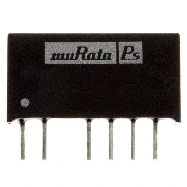
OKR-T/1.5-W12-C产品简介:
ICGOO电子元器件商城为您提供OKR-T/1.5-W12-C由Murata设计生产,在icgoo商城现货销售,并且可以通过原厂、代理商等渠道进行代购。 OKR-T/1.5-W12-C价格参考。MurataOKR-T/1.5-W12-C封装/规格:直流转换器, 非隔离 PoL 模块 DC/DC 转换器 1 输出 0.591 ~ 6 V 1.5A 4.5V - 14V 输入。您可以下载OKR-T/1.5-W12-C参考资料、Datasheet数据手册功能说明书,资料中有OKR-T/1.5-W12-C 详细功能的应用电路图电压和使用方法及教程。
Murata Power Solutions Inc. 的 OKR-T/1.5-W12-C 是一款直流转换器,广泛应用于需要高效、可靠电源转换的各类设备和系统中。该型号属于非隔离式直流-直流转换器(DC-DC Converter),主要功能是将输入的直流电压转换为所需的输出电压,以满足不同负载的需求。

 应用场景:

1. 工业自动化:
   在工业控制系统中,OKR-T/1.5-W12-C 可以为各种传感器、执行器、PLC(可编程逻辑控制器)等提供稳定的电源支持。它能够适应复杂的工业环境,确保设备在高电磁干扰和温度变化的情况下正常工作。

2. 通信设备:
   适用于通信基站、路由器、交换机等网络设备。这些设备通常需要多个不同的电压等级来为内部电路供电,OKR-T/1.5-W12-C 可以提供高效的电压转换,确保通信系统的稳定性和可靠性。

3. 医疗设备:
   医疗仪器如监护仪、便携式诊断设备等对电源要求极高,既要保证安全性,又要确保精度。OKR-T/1.5-W12-C 的低噪声和高稳定性特性使其成为医疗设备的理想选择。

4. 消费电子产品:
   在智能家居、便携式电子设备(如平板电脑、智能手表)中,该转换器可以为电池管理系统、显示屏和其他关键组件提供稳定的电源,延长设备的使用寿命并提高性能。

5. 汽车电子:
   汽车内的各种电子模块如导航系统、娱乐系统、安全系统等都需要可靠的电源支持。OKR-T/1.5-W12-C 能够应对车辆运行中的电压波动和瞬态冲击,确保电子系统的正常工作。

6. 物联网(IoT)设备:
   物联网设备通常需要长时间稳定运行,且功耗较低。OKR-T/1.5-W12-C 的高效能和小体积设计非常适合用于物联网传感器节点、网关等设备,帮助实现节能和小型化设计。

7. 测试与测量仪器:
   精密测试仪器如示波器、信号发生器等对电源的纯净度和稳定性有严格要求。OKR-T/1.5-W12-C 可以提供高质量的电源输出,减少测量误差,提升测试结果的准确性。

总之,OKR-T/1.5-W12-C 凭借其高效、紧凑的设计以及广泛的输入电压范围,适用于多种应用场景,特别是在对电源质量和可靠性要求较高的领域中表现出色。
| 参数 | 数值 |
| 产品目录 | |
| 描述 | DC/DC CONVERTER 0.591-6V 7.5W非隔离式DC/DC转换器 12Vin, 0.591-6Vout 1.5A, Positive Logic |
| 产品分类 | DC DC ConvertersDC/DC转换器 |
| 品牌 | Murata Power Solutions Inc |
| 产品手册 | |
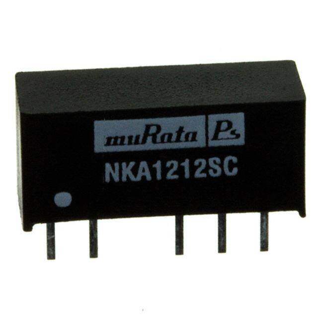
| 产品图片 |
|
| rohs | 符合RoHS无铅 / 符合限制有害物质指令(RoHS)规范要求 |
| 产品系列 | 非隔离式DC/DC转换器,Murata Power Solutions OKR-T/1.5-W12-COkami™ OKL-T/1-W12 |
| 数据手册 | |
| 产品型号 | OKR-T/1.5-W12-C |
| 产品 | Non-Isolated / POL |
| 产品种类 | 非隔离式DC/DC转换器 |
| 其它名称 | 811-2782 |
| 功率(W)-制造系列 | 8W |
| 功率(W)-最大值 | 9W |
| 包装 | 托盘 |
| 商标 | Murata Power Solutions |
| 大小/尺寸 | 0.41" 长 x 0.24" 宽 x 0.40" 高 (10.4mm x 6.1mm x 10.2mm) |
| 安装类型 | 通孔 |
| 安装风格 | Through Hole |
| 宽度 | 10.4 mm |
| 封装 | Tray |
| 封装/外壳 | 5-SIP 模块 |
| 封装/箱体尺寸 | SIP-5 |
| 尺寸 | 10.16 mm x 10.4 mm x 6.1 mm |
| 工作温度 | -40°C ~ 85°C |
| 工作温度范围 | - 40 C to + 85 C |
| 工厂包装数量 | 360 |
| 效率 | 95.5% |
| 标准包装 | 360 |
| 特性 | 远程开/关,OCP,OTP,SCP,UVLO |
| 电压-输入(最大值) | 14V |
| 电压-输入(最小值) | 4.5V |
| 电压-输出1 | 0.591 ~ 6 V |
| 电压-输出2 | - |
| 电压-输出3 | - |
| 电压-隔离 | - |
| 电流-输出(最大值) | 1.5A |
| 类型 | 非隔离 PoL 模块 |
| 输入电压—公称值 | 12 V |
| 输入电压范围 | 4.5 V to 14 V |
| 输出功率 | 7.5 W |
| 输出数 | 1 |
| 输出电压—通道1 | 0.591 V to 6 V |
| 输出电流—通道1 | 1.5 A |
| 输出端数量 | 1 |
| 输出类型 | Adjustable Output |
| 长度 | 10.16 mm |
| 高度 | 6.1 mm |


- 商务部:美国ITC正式对集成电路等产品启动337调查
- 曝三星4nm工艺存在良率问题 高通将骁龙8 Gen1或转产台积电
- 太阳诱电将投资9.5亿元在常州建新厂生产MLCC 预计2023年完工
- 英特尔发布欧洲新工厂建设计划 深化IDM 2.0 战略
- 台积电先进制程称霸业界 有大客户加持明年业绩稳了
- 达到5530亿美元!SIA预计今年全球半导体销售额将创下新高
- 英特尔拟将自动驾驶子公司Mobileye上市 估值或超500亿美元
- 三星加码芯片和SET,合并消费电子和移动部门,撤换高东真等 CEO
- 三星电子宣布重大人事变动 还合并消费电子和移动部门
- 海关总署:前11个月进口集成电路产品价值2.52万亿元 增长14.8%


PDF Datasheet 数据手册内容提取
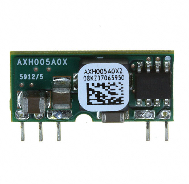
OKR-T/1.5-W12-C www.murata-ps.com Adjustable Output 1.5-Amp SIP-mount DC/DC Converters Typical unit FEATURES PRODUCT OVERVIEW 600 KHz operation The OKR-T/1.5-W12-C is a miniature SIP non-isolated Point-of-Load (PoL) DC/DC power converter measuring only 0.41 x 0.40 x 0.24 inches (10.4 x 10.16 x 6.1 mm). The wide input range is 4.5 to 14 Volts 4.5-14 Vdc input voltage range DC. Based on 600 KHz synchronous buck topology, the high power conversion effi cient Point of Load (PoL) Programmable output voltage from 0.591-6.0 VDC module features programmable output voltage and On/Off control, under voltage lock out (UVLO), overcur- High power conversion effi ciency at 93% rent and over temperature protections. These units are certifi ed to UL/EN/ IEC 60950-1 safety standards (2nd edition) and RoHS-6 hazardous substance compliance. Outstanding thermal derating performance Over temperature and over current protection On/Off control SIP, 0.41 x 0.40 x 0.24 inches (10.4 x 10.16 x 6.1 mm) Certifi ed to UL/EN/IEC 60950-1 safety standards, 2nd edition RoHS-6 hazardous substance compliance Figure 1. Connection Diagram +Vin +Vout F1 (cid:116)(cid:1)(cid:52)(cid:88)(cid:74)(cid:85)(cid:68)(cid:73)(cid:74)(cid:79)(cid:72) (cid:116)(cid:1)(cid:39)(cid:74)(cid:77)(cid:85)(cid:70)(cid:83)(cid:84) Rp On/Off Controller Control (cid:116)(cid:1)(cid:36)(cid:86)(cid:83)(cid:83)(cid:70)(cid:79)(cid:85)(cid:1)(cid:52)(cid:70)(cid:79)(cid:84)(cid:70) External Trim DC Power Q1 Reference and Source Error Amplifier Common Common For full details go to www.murata-ps.com/rohs www.murata-ps.com/support MDC_OKR-T/1.5-W12-C.A01.D5 Page 1 of 16
OKR-T/1.5-W12-C Adjustable Output 1.5-Amp SIP-mount DC/DC Converters PERFORMANCE SPECIFICATIONS SUMMARY AND ORDERING GUIDE Output Input IOUT R/N (mVp-p) Regulation (Max.) IIN, IIN, Effi ciency VOUT (Amps Power VIN Nom. Range no load full load Root Model (Volts) max) (Watts) Max. Line Load (Volts) (Volts) (mA) (Amps) Min. Typ. Dimensions (Inches) OKR-T/1.5-W12-C 0.591-6 1.5 7.5 25 ±0.3% ±0.5% 12 4.5-14 80 0.672 91% 93% 0.41x0.40x0.24 ➀ The input voltage range must be +2V greater for the 3.3V and 5V outputs. ➂ Ripple and Noise (R/N) is shown at Vout=1V. See specs for details. ➁ All specifi cations are at nominal line voltage, Vout=nominal (5V for W12 models) and full load, +25°C unless otherwise noted. PART NUMBER STRUCTURE OK R - T /1.5- W12 - C Okami Non-isolated PoL RoHS Hazardous Substance Compliance C = RoHS-6 (does not claim EU RoHS exemption 7b–lead in solder) SIP-Mount Wide Input Voltage Range W12 = 4.5 – 14 Volts Output Voltage Range Maximum Rated Output T = Trimmable, 0.591-6 Volts Current in Amps Note: Some model number combinations may not be available. Contact Murata Power Solutions for availability. Product Label Because of the small size of these products, the product label contains a Model Number Product Code character-reduced code to indicate the model number and manufacturing date OKR-T/1.5-W12-C 54733 code. Not all items on the label are always used. Please note that the label dif- fers from the product photograph on page 1. Here is the layout of the label: The manufacturing date code is four characters: First character – Last digit of manufacturing year, example 2009 Second character – Month code (1 through 9 = Jan-Sep; XXXXXX Product code Mfg. O, N, D = Oct, Nov, Dec) date YMDX Rev. Revision level code Third character – Day code (1 through 9 = 1 to 9, 10 = 0 and 11 through 31 = A through Z) Figure 2. Label Artwork Layout Fourth character – Manufacturing information The label contains three rows of information: First row – Murata Power Solutions logo Second row – Model number product code (see table) Third row – Manufacturing date code and revision level www.murata-ps.com/support MDC_OKR-T/1.5-W12-C.A01.D5 Page 2 of 16
OKR-T/1.5-W12-C Adjustable Output 1.5-Amp SIP-mount DC/DC Converters FUNCTIONAL SPECIFICATIONS ABSOLUTE MAXIMUM RATINGS Conditions ➀ Minimum Typical/Nominal Maximum Units Input Voltage, Continuous Full power operation 0 15 Vdc Input Reverse Polarity None, install external fuse None Vdc On/Off Remote Control Power on or off, referred to -Vin 0 14 Vdc Output Power 0 7.5 7.65 W Output Current Current-limited, no damage, short-circuit protected 0 1.5 A Storage Temperature Range Vin = Zero (no power) -55 125 °C Absolute maximums are stress ratings. Exposure of devices to greater than any of these conditions may adversely affect long-term reliability. Proper operation under conditions other than those listed in the Performance/Functional Specifi cations Table is not implied or recommended. INPUT Operating voltage range Vin≥Vout+2V for 3.3V and 5V 4.5 12 14 Vdc Recommended External Fuse Fast blow 3 A Turn On/Start-up threshold Rising input voltage 3.9 4.2 4.4 Vdc Turn Off/Undervoltage lockout 15 Falling input voltage 3 3.4 3.7 Vdc Reverse Polarity Protection None, install external fuse None Vdc Internal Filter Type C-TYPE Input current Full Load Conditions Vin = nominal (5Vo set) 0.672 0.701 A Low Line Vin @ min, 5 Vout 1.122 1.163 A Inrush Transient 0.4 A2-Sec. Short Circuit Input Current 60 mA No Load Input Current 5Vout, Iout @ 0 80 100 mA No Load Input Current 0.59V, Iout @ 0 40 55 Shut-Down Mode Input Current 5 mA Refl ected (back) ripple current ➁ Measured at input with specifi ed fi lter 20 mA, pk-pk GENERAL and SAFETY @ Vin nom, 5Vout 91 93 % @ Vin min, 5Vout 94 95.5 % @ Vin nom, 3.3Vout 88.5 90 % @ Vin nom, 2.5Vout 86 88 % Effi ciency @Vin nom, 1.8Vout 82.5 84.5 % @Vin nom, 1.5Vout 80 82.5 % @Vin nom, 1.2Vout 77 79 % @Vin nom, 1Vout 74 76 % Certifi ed to UL-60950-1, IEC/EN60950-1, Safety Yes 2nd Edition Calculated MTBF ➃ Per Telcordia SR332, issue 1, class 3, ground 10.7 Hours x 106 fi xed, Tambient=+25°C DYNAMIC CHARACTERISTICS Fixed Switching Frequency 600 KHz Power On to Vout regulated Startup Time 6 mS (100% resistive load) Startup Time Remote ON to 10% Vout (50% resistive load) 6 8 mS 50-100-50% load step, settling time to within Dynamic Load Response 50 100 μSec ±2% of Vout di/dt = 2.5 A/μSec Dynamic Load Peak Deviation same as above 100 200 mV FEATURES and OPTIONS Remote On/Off Control ➄ “P” suffi x: a 49.2KΩ pulldown to ground needed. Positive Logic, ON state Pin open=ON 2 +Vin V Positive Logic, OFF state 0 0.2 V Control Current open collector/drain 1 mA www.murata-ps.com/support MDC_OKR-T/1.5-W12-C.A01.D5 Page 3 of 16
OKR-T/1.5-W12-C Adjustable Output 1.5-Amp SIP-mount DC/DC Converters FUNCTIONAL SPECIFICATIONS (CONT.) OUTPUT Conditions ➀ Minimum Typical/Nominal Maximum Units Total Output Power 0 7.5 7.65 W Voltage Nominal Output Voltage Range 13 See trim formula 0.591 6 Vdc Setting Accuracy At 50% load -2 2 % of Vnom. Output Voltage Overshoot - Startup: 1 %Vo nom Current Output Current Range 0 1.5 1.5 A Minimum Load No minimum load Current Limit Inception ➅ 98% of Vnom., after warmup @5Vout 2.65 4.15 5.15 A Short Circuit Short Circuit Current ➆ Hiccup technique, autorecovery within 0.6 A ±1% of Vout Short Circuit Duration (remove short for Output shorted to ground, no damage Continuous recovery) Short circuit protection method Current limiting Regulation ➉ Total Regulation Band Over all line, load and temp conditions -3 Vo set 3 % Vo set Line Regulation Vin=min. to max. Vout=nom. ±0.3 % Load Regulation Iout=min. to max. Vin=48V. ±0.5 % 5Vo, 12Vin 75 mV pk-pk 3.3Vo, 12Vin 60 mV pk-pk Ripple and Noise ➇ 1.8Vo, 12Vin 40 mV pk-pk 1Vo, 12Vin 25 mV pk-pk Temperature Coeffi cient At all outputs ±0.02 % of Vnom./°C Maximum Capacitive Loading 14 low ESR; >0.001, <0.01 ohm 200 μF Maximum Capacitive Loading 0.01 ohm 1000 μF MECHANICAL Outline Dimensions 0.41x0.40x0.24 Inches 10.4x10.2x6.1 mm Weight 0.07 Ounces 2 Grams Pin Material copper alloy Pin Finish Pure Matte Tin 200-280 μ" Nickel 40-80 μ'' ENVIRONMENTAL Operating Ambient Temperature Range ➈ full power, all output voltages, -40 85 °C see derating curves Operating PCB Temperature 12 No derating -40 100 °C Storage Temperature Vin = Zero (no power) -55 125 °C Thermal Protection/Shutdown Measured in center 130 130 135 °C Electromagnetic Interference External fi lter required B Conducted, EN55022/CISPR22 Class Radiated, EN55022/CISPR22 B Class Notes: ➀ Specifi cations are typical at +25 deg.C, Vin=nominal (+12V.), Vout=nominal (+5V), full load, external caps and ➇ Output noise may be further reduced by adding an external fi lter. At zero output current, the output may contain natural convection unless otherwise indicated. Extended tests at higher power must supply substantial forced low frequency components which exceed the ripple specifi cation. The output may be operated indefi nitely with airfl ow. All models are tested and specifi ed with external 1 μF paralleled with 10 μF ceramic output capacitors no load. and a 22 μF external input capacitor. All capacitors are low ESR types. These capacitors are necessary to ➈ All models are fully operational and meet published specifi cations, including “cold start” at –40°C. accommodate our test equipment and may not be required to achieve specifi ed performance in your applica- tions. However, Murata Power Solutions recommends installation of these capacitors. All models are stable and ➉ Regulation specifi cations describe the deviation as the line input voltage or output load current is varied from a regulate within spec under no-load conditions. nominal midpoint value to either extreme. ➁ Input Back Ripple Current is tested and specifi ed over a 5 Hz to 20 MHz bandwidth. Input fi ltering is Cin=2 x 100 11 Other input or output voltage ranges will be reviewed under scheduled quantity special order. μF tantalum, Cbus=1000 μF electrolytic, Lbus=1 μH. 12 Maximum PC board temperature is measured with the sensor in the center of the converter. ➂ Note that Maximum Power Derating curves indicate an average current at nominal input voltage. At higher 13 Do not exceed maximum power specifi cations when adjusting the output trim. temperatures and/or lower airfl ow, the DC/DC converter will tolerate brief full current outputs if the total RMS current over time does not exceed the Derating curve. 14 The maximum output capacitive loads depend on the the Equivalent Series Resistance (ESR) of the external output capacitor and, to a lesser extent, the distance and series impedance to the load. Larger caps will reduce ➃ Mean Time Before Failure is calculated using the Telcordia (Belcore) SR-332 Method 1, Case 3, ISSUE 2, output noise but may change the transient response. Newer ceramic caps with very low ESR may require lower ground fi xed controlled conditions, Tambient=+25 deg.C, full output load, natural air convection. capacitor values to avoid instability. Thoroughly test your capacitors in the application. Please refer to the Output ➄ The On/Off Control Input should use either a switch or an open collector/open drain transistor referenced to Capacitive Load Application Note. -Input Common. A logic gate may also be used by applying appropriate external voltages which not exceed +Vin. 15 Do not allow the input voltage to degrade lower than the input undervoltage shutdown voltage at all times. ➅ Short circuit shutdown begins when the output voltage degrades approximately 1% from the selected setting. Otherwise, you risk having the converter turn off. The undervoltage shutdown is not latching and will attempt to ➆ “Hiccup” overcurrent operation repeatedly attempts to restart the converter with a brief, full-current output. If the recover when the input is brought back into normal operating range. overcurrent condition still exists, the restart current will be removed and then tried again. This short current pulse 16 The outputs are not intended to sink appreciable reverse current. prevents overheating and damaging the converter. Once the fault is removed, the converter immediately recovers normal operation. www.murata-ps.com/support MDC_OKR-T/1.5-W12-C.A01.D5 Page 4 of 16
OKR-T/1.5-W12-C Adjustable Output 1.5-Amp SIP-mount DC/DC Converters OKR-T/1.5-W12-C PERFORMANCE DATA Effi ciency vs. Line Voltage and Load Current @ 25°C (Vin = 1V) Effi ciency vs. Line Voltage and Load Current @ 25°C (Vin = 2.5V) 90 100 80 90 80 70 70 60 VIN = 14V VIN = 14V VIN = 12V 60 VIN = 12V %)50 VIN = 4.5V %) VIN = 4.5V ficiency (40 ficiency ( 4500 Ef Ef 30 30 20 20 10 10 0 0 0 0.2 0.4 0.6 0.8 1 1.2 1.4 1.6 0 0.2 0.4 0.6 0.8 1 1.2 1.4 1.6 Load Current (Amps) Load Current (Amps) Effi ciency vs. Line Voltage and Load Current @ 25°C (Vin = 3.3V) Effi ciency vs. Line Voltage and Load Current @ 25°C (Vin = 5V) 100 100 90 90 80 80 VIN = 14V 6700 VVIINN == 1142VV 6700 VVIINN == 172VV %) VIN = 5.5V %) ncy ( 50 ncy (50 ficie 40 ficie40 Ef Ef 30 30 20 20 10 10 0 0 0 0.2 0.4 0.6 0.8 1 1.2 1.4 1.6 0 0.2 0.4 0.6 0.8 1 1.2 1.4 1.6 Load Current (Amps) Load Current (Amps) OKR-T/1.5-W12-C OSCILLOGRAMS Maximum Current Temperature Derating @ Sea Level On/Off Enable Startup (Vin=12V, Vout=1.5V, Iout=1.5A, Cload=0) (VIN = 7V and 12V, VOUT = 5V and 6 V) Channel 2=Enable, Channel 1=Vout 4.0 3.5 3.0 Amps) 2.5 nt ( urre 2.0 C put 1.5 Out Natural convection 1.0 0.5 0.0 20 25 30 35 40 45 50 55 60 65 70 75 80 85 90 Ambient Temperature (ºC) There is no derating for Vout = 0.591V. to 5.5V. at full load. www.murata-ps.com/support MDC_OKR-T/1.5-W12-C.A01.D5 Page 5 of 16
OKR-T/1.5-W12-C Adjustable Output 1.5-Amp SIP-mount DC/DC Converters OKR-T/1.5-W12-C OSCILLOGRAMS – Vout = 1.8V Step Load Transient Response (Vin=12V, Vout=1.8V, Cload=5x10μF Step Load Transient Response (Vin=12V, Vout=1.8V, Cload=5x10μF X5R 0805 ceramic, total 50μF, Iout=0A to 1.5A) Top trace=Vout, Bottom trace=Iout X5R 0805 ceramic, total 50μF, Iout=1.5A to 0A) Top trace=Vout, Bottom trace=Iout Step Load Transient Response (Vin=4.5V, Vout=1.8V, Cload=5x10μF Step Load Transient Response (Vin=4.5V, Vout=1.8V, Cload=5x10μF X5R 0805 ceramic, total 50μF, Iout=0A to 1.5A) Top trace=Vout, Bottom trace=Iout X5R 0805 ceramic, total 50μF, Iout=1.5A to 0A) Top trace=Vout, Bottom trace=Iout Step Load Transient Response (Vin=12V, Vout=1.8V, Cload=12x10μF Step Load Transient Response (Vin=12V, Vout=1.8V, Cload=12x10μF X5R 0805 ceramic, total 120μF, Iout=0A to 1.5A) Top trace=Vout, Bottom trace=Iout X5R 0805 ceramic, total 120μF, Iout=1.5A to 0A) Top trace=Vout, Bottom trace=Iout www.murata-ps.com/support MDC_OKR-T/1.5-W12-C.A01.D5 Page 6 of 16
OKR-T/1.5-W12-C Adjustable Output 1.5-Amp SIP-mount DC/DC Converters OKR-T/1.5-W12-C OSCILLOGRAMS – Vout = 1.8V Step Load Transient Response (Vin=4.5V, Vout=1.8V, Cload=12x10μF Step Load Transient Response (Vin=4.5V, Vout=1.8V, Cload=12x10μF X5R 0805 ceramic, total 120μF, Iout=0A to 1.5A) Top trace=Vout, Bottom trace=Iout X5R 0805 ceramic, total 120μF, Iout=1.5A to 0A) Top trace=Vout, Bottom trace=Iout Step Load Transient Response (Vin=4.5V, Vout=1.8V, Cload=10x10μF X5R 0805 ceramic, plus Step Load Transient Response (Vin=4.5V, Vout=1.8V, Cload=10x10μF X5R 0805 ceramic, plus 1x470μF, 7mΩ POSCAP, total 570μF, Iout=0A to 1.5A) Top trace=Vout, Bottom trace=Iout 1x470μF, 7mΩ POSCAP, total 570μF, Iout=1.5A to 0A) Top trace=Vout, Bottom trace=Iout Step Load Transient Response (Vin=12V, Vout=1.8V, Cload=10x10μF X5R 0805 ceramic, plus Step Load Transient Response (Vin=12V, Vout=1.8V, Cload=10x10μF X5R 0805 ceramic, plus 1x470μF, 7mΩ POSCAP, total 570μF, Iout=0A to 1.5A) Top trace=Vout, Bottom trace=Iout 1x470μF, 7mΩ POSCAP, total 570μF, Iout=1.5A to 0A) Top trace=Vout, Bottom trace=Iout www.murata-ps.com/support MDC_OKR-T/1.5-W12-C.A01.D5 Page 7 of 16
OKR-T/1.5-W12-C Adjustable Output 1.5-Amp SIP-mount DC/DC Converters OKR-T/1.5-W12-C OSCILLOGRAMS – Vout = 3.3V Step Load Transient Response (Vin=12V, Vout=3.3V, Cload=5x10μF Step Load Transient Response (Vin=12V, Vout=3.3V, Cload=5x10μF X5R 0805 ceramic, total 50μF, Iout=0A to 1.5A) Top trace=Vout, Bottom trace=Iout X5R 0805 ceramic, total 50μF, Iout=1.5A to 0A) Top trace=Vout, Bottom trace=Iout Step Load Transient Response (Vin=5.5V, Vout=3.3V, Cload=5x10μF Step Load Transient Response (Vin=5.5V, Vout=3.3V, Cload=5x10μF X5R 0805 ceramic, total 50μF, Iout=0A to 1.5A) Top trace=Vout, Bottom trace=Iout X5R 0805 ceramic, total 50μF, Iout=1.5A to 0A) Top trace=Vout, Bottom trace=Iout Step Load Transient Response (Vin=12V, Vout=3.3V, Cload=12x10μF Step Load Transient Response (Vin=12V, Vout=3.3V, Cload=12x10μF X5R 0805 ceramic, total 120μF, Iout=0A to 1.5A) Top trace=Vout, Bottom trace=Iout X5R 0805 ceramic, total 120μF, Iout=1.5A to 0A) Top trace=Vout, Bottom trace=Iout www.murata-ps.com/support MDC_OKR-T/1.5-W12-C.A01.D5 Page 8 of 16
OKR-T/1.5-W12-C Adjustable Output 1.5-Amp SIP-mount DC/DC Converters OKR-T/1.5-W12-C OSCILLOGRAMS – Vout = 3.3V Step Load Transient Response (Vin=5.5V, Vout=3.3V, Cload=12x10μF Step Load Transient Response (Vin=5.5V, Vout=3.3V, Cload=12x10μF X5R 0805 ceramic, total 120μF, Iout=0A to 1.5A) Top trace=Vout, Bottom trace=Iout X5R 0805 ceramic, total 120μF, Iout=1.5A to 0A) Top trace=Vout, Bottom trace=Iout Step Load Transient Response (Vin=5.5V, Vout=3.3V, Cload=10x10μF X5R 0805 ceramic, plus Step Load Transient Response (Vin=5.5V, Vout=3.3V, Cload=10x10μF X5R 0805 ceramic, plus 1x470μF, 7mΩ POSCAP, total 570μF, Iout=0A to 1.5A) Top trace=Vout, Bottom trace=Iout 1x470μF, 7mΩ POSCAP, total 570μF, Iout=1.5A to 0A) Top trace=Vout, Bottom trace=Iout Step Load Transient Response (Vin=12V, Vout=3.3V, Cload=10x10μF X5R 0805 ceramic, plus Step Load Transient Response (Vin=12V, Vout=3.3V, Cload=10x10μF 5R 0805 ceramic, plus 1x470μF, 7mΩ POSCAP, total 570μF, Iout=0A to 1.5A) Top trace=Vout, Bottom trace=Iout 1x470μF, 7mΩ POSCAP, total 570μF, Iout=1.5A to 0A) Top trace=Vout, Bottom trace=Iout www.murata-ps.com/support MDC_OKR-T/1.5-W12-C.A01.D5 Page 9 of 16
OKR-T/1.5-W12-C Adjustable Output 1.5-Amp SIP-mount DC/DC Converters OKR-T/1.5-W12-C OSCILLOGRAMS – Vout = 5V Step Load Transient Response (Vin=12V, Vout=5V, Cload=5x10μF X5R Step Load Transient Response (Vin=12V, Vout=5V, Cload=5x10μF 0805 ceramic, total 50μF, Iout=0A to 1.5A) Top trace=Vout, Bottom trace=Iout X5R 0805 ceramic, total 50μF, Iout=1.5A to 0A) Top trace=Vout, Bottom trace=Iout Step Load Transient Response (Vin=7.5V, Vout=5V, Cload=5x10μF Step Load Transient Response (Vin=7.5V, Vout=5V, Cload=5x10μF X5R X5R 0805 ceramic, total 50μF, Iout=0A to 1.5A) Top trace=Vout, Bottom trace=Iout 0805 ceramic, total 50μF, Iout=1.5A to 0A) Top trace=Vout, Bottom trace=Iout Step Load Transient Response (Vin=12V, Vout=5V, Cload=12x10μF Step Load Transient Response (Vin=12V, Vout=5V, Cload=12x10μF X5R 0805 ceramic, total 120μF, Iout=0A to 1.5A) Top trace=Vout, Bottom trace=Iout X5R 0805 ceramic, total 120μF, Iout=1.5A to 0A) Top trace=Vout, Bottom trace=Iout www.murata-ps.com/support MDC_OKR-T/1.5-W12-C.A01.D5 Page 10 of 16
OKR-T/1.5-W12-C Adjustable Output 1.5-Amp SIP-mount DC/DC Converters OKR-T/1.5-W12-C OSCILLOGRAMS – Vout = 5V Step Load Transient Response (Vin=7.5V, Vout=5V, Cload=12x10μF Step Load Transient Response (Vin=7.5V, Vout=5V, Cload=12x10μF X5R 0805 ceramic, total 120μF, Iout=0A to 1.5A) Top trace=Vout, Bottom trace=Iout X5R 0805 ceramic, total 120μF, Iout=1.5A to 0A) Top trace=Vout, Bottom trace=Iout Step Load Transient Response (Vin=7.5V, Vout=5V, Cload=10x10μF X5R 0805 ceramic, plus Step Load Transient Response (Vin=7.5V, Vout=5V, Cload=10x10μF X5R 0805 ceramic, plus 1x470μF, 7mΩ POSCAP, total 570μF, Iout=0A to 1.5A) Top trace=Vout, Bottom trace=Iout 1x470μF, 7mΩ POSCAP, total 570μF, Iout=1.5A to 0A) Top trace=Vout, Bottom trace=Iout Step Load Transient Response (Vin=12V, Vout=5V, Cload=10x10μF X5R 0805 ceramic, plus Step Load Transient Response (Vin=12V, Vout=5V, Cload=10x10μF X5R 0805 ceramic, plus 1x470μF, 7mΩ POSCAP, total 570μF, Iout=0A to 1.5A) Top trace=Vout, Bottom trace=Iout 1x470μF, 7mΩ POSCAP, total 570μF, Iout=1.5A to 0A) Top trace=Vout, Bottom trace=Iout www.murata-ps.com/support MDC_OKR-T/1.5-W12-C.A01.D5 Page 11 of 16
OKR-T/1.5-W12-C Adjustable Output 1.5-Amp SIP-mount DC/DC Converters MECHANICAL SPECIFICATIONS 0.24 (6.1) 0.41 (10.4) REF 0.11 C 0.205 L (2.79) 0.05 (5.2) (1.3) REF REF THK 0.40 (10.16) Pin #1 0.15 (3.8) Pin #5 0.067 (1.7) 0.14 (3.56) 0.134 (3.4) 0.067 (1.7) 0.032 ±.002 TYP 0.134 (3.4) (0.813) Pin #1 Dimensions are in inches (mm shown for ref. only). Third Angle Projection Tolerances (unless otherwise specified): .XX ± 0.02 (0.5) .XXX ± 0.010 (0.25) Angles ± 2˚ Components are shown for reference only. 0.42 (10.67) 5X 0.047±.005 0.21 (1.19) (5.33) INPUT/OUTPUT CONNECTIONS OKR-T/1.5-W12-C 0.150 .26 MIN (3.81) Pin Function 1 Remote On/Off Control* 1 2 3 4 5 2 +VIN 3 Ground (Common) 4 +VOUT RECOMMENDED FOOTPRINT 5 Trim (VIEWED FROM TOP) * The Remote On/Off can be provided with either Figure 3. OKR-T/1.5-W12-C positive (P suffi x) or negative (N suffi x) logic. Component locations are typical. www.murata-ps.com/support MDC_OKR-T/1.5-W12-C.A01.D5 Page 12 of 16
OKR-T/1.5-W12-C Adjustable Output 1.5-Amp SIP-mount DC/DC Converters STANDARD PACKAGING Each static dissipative polyethylene foam tray accommodates 120 converters 2.5±.25 (63.5) Closed height 10.00 ±.25 10.00±.25 (254.0) (254.0) Carton accommodates four (3) trays of 120 yielding 360 converters per carton. 9.92 0.63 (16.0) (252.0) 6.5 X 45° 0.39 (10.0) 0.49 x4 (12.5) 0.94 (24.0) 9.92 (252.0) 0.2 (5.0) 0.33 0.43 0.2 (8.5) (11.0) (5.0) Dimensions are in inches (mm shown for ref. only). Third Angle Projection Notes: 1. Material: Dow 220 antistat ethafoam (Density: 34-35 kg/m3) Tolerances (unless otherwise specified): .XX ± 0.02 (0.5) 2. Dimensions: 252 x 252 x 16 mm .XXX ± 0.010 (0.25) 8 x 15 array (120 per tray) Angles ± 2˚ Components are shown for reference only. www.murata-ps.com/support MDC_OKR-T/1.5-W12-C.A01.D5 Page 13 of 16
OKR-T/1.5-W12-C Adjustable Output 1.5-Amp SIP-mount DC/DC Converters suggested capacitor values are 10 to 22 μF, rated at twice the expected maxi- TECHNICAL NOTES mum input voltage. Make sure that the input terminals do not go below the Input Fusing undervoltage shutdown voltage at all times. More input bulk capacitance may Certain applications and/or safety agencies may require fuses at the inputs of be added in parallel (either electrolytic or tantalum) if needed. power conversion components. Fuses should also be used when there is the Recommended Output Filtering possibility of sustained input voltage reversal which is not current-limited. For The minimum external output capacitance required for proper operation greatest safely, we recommend a fast blow fuse installed in the ungrounded is 50uF ceramic type. The maximum external output capacitance is 100uF input supply line. ceramic and 470uF POSCAP. Operating outside of these minimum and maxi- The installer must observe all relevant safety standards and regulations. For mum limits may affect the performance of the unit. safety agency approvals, install the converter in compliance with the end-user Input Ripple Current and Output Noise safety standard, i.e. IEC/EN/UL 60950-1. All models in this converter series are tested and specifi ed for input refl ected Input Under-Voltage Shutdown and Start-Up Threshold ripple current and output noise using designated external input/output compo- Under normal start-up conditions, converters will not begin to regulate properly nents, circuits and layout as shown in the fi gures below. In the fi gure below, until the ramping-up input voltage exceeds and remains at the Start-Up the Cbus and Lbus components simulate a typical DC voltage bus. Please Threshold Voltage (see Specifi cations). Once operating, converters will not note that the values of Cin, Lbus and Cbus will vary according to the specifi c turn off until the input voltage drops below the Under-Voltage Shutdown Limit. converter model. Subsequent restart will not occur until the input voltage rises again above the Start-Up Threshold. This built-in hysteresis prevents any unstable on/off opera- TO tion at a single input voltage. OSCILLOSCOPE CURRENT PROBE Users should be aware however of input sources near the Under-Voltage +VIN Shutdown whose voltage decays as input current is consumed (such as + LBUS capacitor inputs), the converter shuts off and then restarts as the external capacitor recharges. Such situations could oscillate. To prevent this, make VIN +– CBUS CIN sure the operating input voltage is well above the UV Shutdown voltage AT ALL – TIMES. -VIN Start-Up Time CIN = 2 x 100μF, ESR < 700mΩ @ 100kHz Assuming that the output current is set at the rated maximum, the Vin to Vout CBUS = 1000μF, ESR < 100mΩ @ 100kHz Start-Up Time (see Specifi cations) is the time interval between the point when LBUS = 1μH the ramping input voltage crosses the Start-Up Threshold and the fully loaded regulated output voltage enters and remains within its specifi ed accuracy band. Figure 4. Measuring Input Ripple Current Actual measured times will vary with input source impedance, external input capacitance, input voltage slew rate and fi nal value of the input voltage as it appears at the converter. These converters include a soft start circuit to moderate the duty cycle of its PWM controller at power up, thereby limiting the input inrush current. +VOUT The On/Off Remote Control interval from On command to Vout regulated assumes that the converter already has its input voltage stabilized above the Start-Up Threshold before the On command. The interval is measured from the C1 C2 SCOPE RLOAD On command until the output enters and remains within its specifi ed accuracy band. The specifi cation assumes that the output is fully loaded at maximum -VOUT rated current. Similar conditions apply to the On to Vout regulated specifi cation such as external load capacitance and soft start circuitry. Recommended Input Filtering C1 = 1μF The user must assure that the input source has low AC impedance to provide C2 = 10μF dynamic stability and that the input supply has little or no inductive content, LOAD 2-3 INCHES (51-76mm) FROM MODULE including long distributed wiring to a remote power supply. The converter will Figure 5. Measuring Output Ripple and Noise (PARD) operate with no additional external capacitance if these conditions are met. For best performance, we recommend installing a low-ESR capacitor immediately adjacent to the converter’s input terminals. The capacitor should be a ceramic type such as the Murata GRM32 series or a polymer type. Initial www.murata-ps.com/support MDC_OKR-T/1.5-W12-C.A01.D5 Page 14 of 16
OKR-T/1.5-W12-C Adjustable Output 1.5-Amp SIP-mount DC/DC Converters Minimum Output Loading Requirements CAUTION: If you routinely or accidentally exceed these Derating guidelines, All models regulate within specifi cation and are stable under no load to full the converter may have an unplanned Over Temperature shut down. Also, these load conditions. Operation under no load might however slightly increase graphs are all collected at slightly above Sea Level altitude. Be sure to reduce output ripple and noise. the derating for higher density altitude. Thermal Shutdown Output Current Limiting To prevent many over temperature problems and damage, these converters Current limiting inception is defi ned as the point at which full power falls below include thermal shutdown circuitry. If environmental conditions cause the the rated tolerance. See the Performance/Functional Specifi cations. Note par- temperature of the DC/DC’s to rise above the Operating Temperature Range ticularly that the output current may briefl y rise above its rated value in normal up to the shutdown temperature, an on-board electronic temperature sensor operation as long as the average output power is not exceeded. This enhances will power down the unit. When the temperature decreases below the turn-on reliability and continued operation of your application. If the output current is threshold, the converter will automatically restart. There is a small amount of too high, the converter will enter the short circuit condition. hysteresis to prevent rapid on/off cycling. The temperature sensor is typically Output Short Circuit Condition located adjacent to the switching controller, approximately in the center of the When a converter is in current-limit mode, the output voltage will drop as the unit. See the Performance and Functional Specifi cations. output current demand increases. If the output voltage drops too low (approxi- CAUTION: If you operate too close to the thermal limits, the converter may mately 98% of nominal output voltage for most models), the magnetically shut down suddenly without warning. Be sure to thoroughly test your applica- coupled voltage used to develop primary side voltages will also drop, thereby tion to avoid unplanned thermal shutdown. shutting down the PWM controller. Following a time-out period, the PWM will restart, causing the output voltage to begin ramping up to its appropriate value. Temperature Derating Curves If the short-circuit condition persists, another shutdown cycle will initiate. This The graphs in this data sheet illustrate typical operation under a variety of rapid on/off cycling is called “hiccup mode”. The hiccup cycling reduces the conditions. The Derating curves show the maximum continuous ambient air average output current, thereby preventing excessive internal temperatures temperature and decreasing maximum output current which is acceptable and/or component damage. A short circuit can be tolerated indefi nitely. under increasing forced airfl ow measured in Linear Feet per Minute (“LFM”). Note that these are AVERAGE measurements. The converter will accept brief The “hiccup” system differs from older latching short circuit systems increases in current or reduced airfl ow as long as the average is not exceeded. because you do not have to power down the converter to make it restart. The system will automatically restore operation as soon as the short circuit condi- Note that the temperatures are of the ambient airfl ow, not the converter tion is removed. itself which is obviously running at higher temperature than the outside air. Also note that very low fl ow rates (below about 25 LFM) are similar to “natural convection,” that is, not using fan-forced airfl ow. Murata Power Solutions makes Characterization measurements in a closed cycle wind tunnel with calibrated airfl ow. We use both thermocouples and an infrared camera system to observe thermal performance. www.murata-ps.com/support MDC_OKR-T/1.5-W12-C.A01.D5 Page 15 of 16
OKR-T/1.5-W12-C Adjustable Output 1.5-Amp SIP-mount DC/DC Converters Trim Connections Output Voltage Adustment The output voltage may be adjusted over a limited range by connecting an external trim resistor (Rtrim) between the Trim pin and Ground. The Rtrim +VOUT resistor must be a 1/10 Watt precision metal fi lm type, ±0.5% accuracy or better with low temperature coeffi cient, ±100 ppm/oC. or better. Mount the RTRIM resistor close to the converter with very short leads or use a surface mount Trim RLOAD trim resistor. Ground In the tables below, the calculated resistance is given. Do not exceed the specifi ed limits of the output voltage or the converter’s maximum power 1.182 rating when applying these resistors. Also, avoid high noise at the Trim RTRIM (kΩ) = VOUT − 0.591 input. However, to prevent instability, you should never connect any capaci- tors to Trim. OKR-T/1.5-W12-C Resistor Trim Equation, OKR-T/1.5-W12-C models: Output Voltage Calculated Rtrim (Ω) 6 V. 218.5 RTRIM (k) = ____1_.1_8_2______ (VOUT – 0.591) 5 V. 268 3.3 V. 436 2.5 V. 619 1.8 V. 978 1.5 V. 1300 1.2 V. 1940 1.0 V. 2890 0.591 V. ∞ (open) Soldering Guidelines Murata Power Solutions recommends the specifi cations below when installing these converters. These specifi cations vary depending on the solder type. Exceeding these specifi ca- tions may cause damage to the product. Your production environment may differ; therefore please thoroughly review these guidelines with your process engineers. Wave Solder Operations for through-hole mounted products (THMT) For Sn/Ag/Cu based solders: For Sn/Pb based solders: Maximum Preheat Temperature 115° C. Maximum Preheat Temperature 105° C. Maximum Pot Temperature 270° C. Maximum Pot Temperature 250° C. Maximum Solder Dwell Time 7 seconds Maximum Solder Dwell Time 6 seconds This product is subject to the following operating requirements Murata Power Solutions, Inc. and the Life and Safety Critical Application Sales Policy: 11 Cabot Boulevard, Mansfi eld, MA 02048-1151 U.S.A. Refer to: http://www.murata-ps.com/requirements/ ISO 9001 and 14001 REGISTERED Murata Power Solutions, Inc. makes no representation that the use of its products in the circuits described herein, or the use of other technical information contained herein, will not infringe upon existing or future patent rights. The descriptions contained herein do not imply the granting of licenses to make, use, or sell equipment constructed in accordance therewith. Specifi cations are subject to change without notice. © 2012 Murata Power Solutions, Inc. www.murata-ps.com/support MDC_OKR-T/1.5-W12-C.A01.D5 Page 16 of 16
Mouser Electronics Authorized Distributor Click to View Pricing, Inventory, Delivery & Lifecycle Information: M urata: OKR-T/1.5-W12-C