
 Datasheet下载
- 型号: OKL-T/3-W12P-C
- 制造商: Murata
- 库位|库存: xxxx|xxxx
- 要求:
| 数量阶梯 | 香港交货 | 国内含税 |
| +xxxx | $xxxx | ¥xxxx |
查看当月历史价格
查看今年历史价格
OKL-T/3-W12P-C产品简介:
ICGOO电子元器件商城为您提供OKL-T/3-W12P-C由Murata设计生产,在icgoo商城现货销售,并且可以通过原厂、代理商等渠道进行代购。 OKL-T/3-W12P-C价格参考¥38.19-¥43.12。MurataOKL-T/3-W12P-C封装/规格:直流转换器, 非隔离 PoL 模块 DC/DC 转换器 1 输出 0.591 ~ 5.5 V 3A 4.5V - 14V 输入。您可以下载OKL-T/3-W12P-C参考资料、Datasheet数据手册功能说明书,资料中有OKL-T/3-W12P-C 详细功能的应用电路图电压和使用方法及教程。
Murata Power Solutions Inc. 的 OKL-T/3-W12P-C 是一款直流转换器,主要用于工业、通信和消费电子领域。该型号的转换器具有高效能、高可靠性和紧凑设计的特点,适用于多种应用场景。

 1. 工业自动化
在工业自动化系统中,OKL-T/3-W12P-C 可以为各种传感器、执行器和控制器提供稳定的电源。它能够将输入的直流电压转换为所需的输出电压,确保设备在复杂电磁环境中稳定工作。例如,在工厂自动化生产线中,这款转换器可以为PLC(可编程逻辑控制器)、HMI(人机界面)和其他关键组件供电,保证系统的正常运行。

 2. 通信设备
对于通信设备而言,电源的稳定性至关重要。OKL-T/3-W12P-C 能够为路由器、交换机、基站等通信设备提供可靠的电源支持。它具备良好的抗干扰能力和宽泛的工作温度范围,能够在恶劣环境下保持性能稳定。此外,其高效的转换效率有助于降低功耗,减少散热需求,延长设备使用寿命。

 3. 医疗设备
在医疗设备中,电源的安全性和可靠性是首要考虑因素。OKL-T/3-W12P-C 可以为便携式医疗仪器、监护仪、诊断设备等提供稳定的电源。其紧凑的设计使其适合用于空间有限的医疗设备中,而高效能则有助于提高设备的整体性能,确保患者数据的准确性和安全性。

 4. 消费电子产品
在消费电子产品中,如笔记本电脑、平板电脑和智能家居设备,OKL-T/3-W12P-C 可以作为内部电源模块使用。它的高效转换效率和小尺寸设计使得它非常适合应用于对体积和功耗有严格要求的产品中。此外,其低噪声特性也有助于提升用户体验,减少电磁干扰对其他功能的影响。

 5. 汽车电子
在汽车电子领域,OKL-T/3-W12P-C 可以为车载信息系统、娱乐系统和辅助驾驶系统提供稳定的电源。它能够在车辆启动时承受较大的电压波动,并在行驶过程中保持稳定的输出,确保电子系统的正常工作。

总之,OKL-T/3-W12P-C 直流转换器凭借其高效能、高可靠性和紧凑设计,广泛应用于工业、通信、医疗、消费电子和汽车等多个领域,为各类设备提供稳定可靠的电源支持。
| 参数 | 数值 |
| 产品目录 | |
| 描述 | CONV DC/DC 15W 12VIN 3AOUT SMD非隔离式DC/DC转换器 12Vin 0.591-5.5Vout 3A 15W Pos Polarity |
| 产品分类 | DC DC ConvertersDC/DC转换器 |
| 品牌 | Murata Power Solutions |
| 产品手册 | |
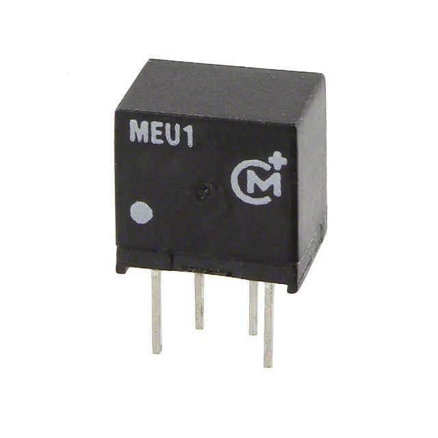
| 产品图片 |
|
| rohs | 符合RoHS无铅 / 符合限制有害物质指令(RoHS)规范要求 |
| 产品系列 | 非隔离式DC/DC转换器,Murata Power Solutions OKL-T/3-W12P-COkami™ OKL-T/3-W12 |
| 数据手册 | |
| 产品型号 | OKL-T/3-W12P-C |
| 产品 | Non-Isolated / POL |
| 产品种类 | 非隔离式DC/DC转换器 |
| 其它名称 | 811-2709-6 |
| 功率(W)-制造系列 | 15W |
| 功率(W)-最大值 | 15W |
| 包装 | Digi-Reel® |
| 商标 | Murata Power Solutions |
| 大小/尺寸 | 0.48" 长 x 0.48" 宽 x 0.25" 高(12.2mm x 12.2mm x 6.4mm) |
| 安装类型 | 表面贴装 |
| 安装风格 | SMD/SMT |
| 封装 | Reel |
| 封装/外壳 | 12-SMD 模块 |
| 封装/箱体尺寸 | 12.2 mm x 12.2 mm x 6.4 mm |
| 工作温度 | -40°C ~ 85°C |
| 工厂包装数量 | 400 |
| 效率 | 93% |
| 标准包装 | 1 |
| 特性 | 远程开/关,OCP,OTP,SCP,UVLO |
| 电压-输入(最大值) | 14V |
| 电压-输入(最小值) | 4.5V |
| 电压-输出1 | 0.591 ~ 5.5 V |
| 电压-输出2 | - |
| 电压-输出3 | - |
| 电压-隔离 | - |
| 电流-输出(最大值) | 3A |
| 类型 | 非隔离 PoL 模块 |
| 系列 | Okami |
| 输入电压—公称值 | 12 V |
| 输入电压范围 | 4.5 V to 14 V |
| 输出功率 | 15 W |
| 输出数 | 1 |
| 输出电压—通道1 | 0.591 V to 5.5 V |
| 输出电流—通道1 | 3 A |
| 输出端数量 | 1 |
| 输出类型 | Adjustable Output DC/DC Converters |


- 商务部:美国ITC正式对集成电路等产品启动337调查
- 曝三星4nm工艺存在良率问题 高通将骁龙8 Gen1或转产台积电
- 太阳诱电将投资9.5亿元在常州建新厂生产MLCC 预计2023年完工
- 英特尔发布欧洲新工厂建设计划 深化IDM 2.0 战略
- 台积电先进制程称霸业界 有大客户加持明年业绩稳了
- 达到5530亿美元!SIA预计今年全球半导体销售额将创下新高
- 英特尔拟将自动驾驶子公司Mobileye上市 估值或超500亿美元
- 三星加码芯片和SET,合并消费电子和移动部门,撤换高东真等 CEO
- 三星电子宣布重大人事变动 还合并消费电子和移动部门
- 海关总署:前11个月进口集成电路产品价值2.52万亿元 增长14.8%

PDF Datasheet 数据手册内容提取
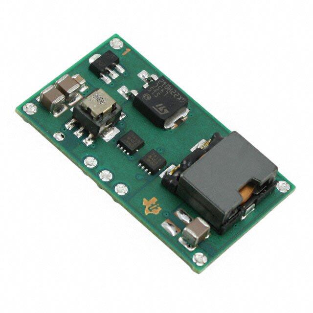
OKL-T/3-W12 Series www.murata-ps.com Programmable Output 3-Amp iLGA SMT PoLs Typical unit FEATURES PRODUCT OVERVIEW iLGA inspectable Land Grid Array The OKL-T/3-W12 series are miniature effi cient Point of Load (PoL) module features non -isolated Point-of-Load (PoL) DC/DC power programmable output voltage and On/Off control. 4.5-14Vdc input voltage range converters for embedded applications. Featuring These converters also include under voltage lock Programmable output voltage from 0.591-5.5Vdc inspectable Land Grid Array (iLGA) format, the out (UVLO), output short circuit protection, and Drives up to 200 μF ceramic capacitive loads OKL-T/3-W12 measures only 0.48 x 0.48 x 0.244 over-current protections. inches max. (12.2 x 12.2 x 6.2 mm max.). An optional sequence/tracking feature on High power conversion effi ciency at 93% The wide input range is 4.5 to 14 Volts DC. OKL2-T/3-W12 models allows power sequencing of Outstanding thermal derating performance The maximum output current is 3 Amps. Based PoL’s. These units are certifi ed to all standard UL/EN/ Short circuit and over current protection on fi xed-frequency synchronous buck converter IEC 60950-1 safety certifi cations (2nd Edition) and switching topology, the high power conversion RoHS-6 hazardous substance compliance. On/Off control and Power Good signal Optional Sequence/Tracking operation (OKL2-T/3-W12 models) Certifi ed to UL/EN/IEC 60950-1 safety, 2nd Edition RoHS-6 hazardous substance compliance Connection Diagram +Vin +Vout F1 (cid:116)(cid:1)(cid:52)(cid:88)(cid:74)(cid:85)(cid:68)(cid:73)(cid:74)(cid:79)(cid:72) On/Off Sense Control (cid:116)(cid:1)(cid:39)(cid:74)(cid:77)(cid:85)(cid:70)(cid:83)(cid:84) Controller (cid:116)(cid:1)(cid:36)(cid:86)(cid:83)(cid:83)(cid:70)(cid:79)(cid:85)(cid:1)(cid:52)(cid:70)(cid:79)(cid:84)(cid:70) External Trim DC Power Open = On Reference and Source Closed = Off Error Amplifier (Positive On/Off) Common Common Sequence/Tracking Power Good (OKL2 Models) Figure 1. OKL-T/3-W12 Note: Murata Power Solutions strongly recommends an external input fuse, F1. See specifi cations. For full details go to www.murata-ps.com/rohs www.murata-ps.com/support MDC_OKL-T/3-W12 Series.C03 Page 1 of 17
OKL-T/3-W12 Series Programmable Output 3-Amp iLGA SMT PoLs Performance Specifi cations and Ordering Guide ORDERING GUIDE Output Input Package - Pinout P83 Effi ciency On/Off Seq/ Model Number Vout Iout (Amps, Power R/N (mV p-p) Regulation (max.) Vin nom. Range Iin, no load Iin, full load Logic Track Case C83 (Volts) ➀ max.) (Watts) Max. ➃ Line Load (Volts) (Volts) (mA) ➃ (Amps) ➁ Min. Typ. inches (mm) 0.48x0.48x0.244 max OKL-T/3-W12P-C 0.591-5.5 3 15.0 37 ±0.25% ±0.25% 12 4.5-14 20 1.34 91% 93% Pos. no 12.2x12.2x6.2 max 0.48x0.48x0.244 max OKL-T/3-W12N-C 0.591-5.5 3 15.0 37 ±0.25% ±0.25% 12 4.5-14 20 1.34 91% 93% Neg. no 12.2x12.2x6.2 max 0.48x0.48x0.244 max OKL2-T/3-W12P-C 0.591-5.5 3 15.0 37 ±0.25% ±0.25% 12 4.5-14 20 1.34 91% 93% Pos. yes 12.2x12.2x6.2 max 0.48x0.48x0.244 max OKL2-T/3-W12N-C 0.591-5.5 3 15.0 37 ±0.25% ±0.25% 12 4.5-14 20 1.34 91% 93% Neg. yes 12.2x12.2x6.2 max ➀ The output range is limited by Vin. See detailed specs. I/O caps are necessary for our test equipment and may not be needed for your application. ➁ All specifi cations are at nominal line voltage, Vout=nominal (5V for W12 models) and full load, ➂ Use adequate ground plane and copper thickness adjacent to the converter. +25 deg.C. unless otherwise noted. Ripple and Noise (R/N) and no-load input current are shown at Vout=1V. See specs for details. Output capacitors are 10 μF ceramic. Input cap is 22 μF. See detailed specifi cations. PART NUMBER STRUCTURE OK L 2 - T / 3 -W12 N - C Non-isolated PoL LGA Surface Mount Sequence/tracking RoHS Hazardous Blank = Not installed Substance Compliance 2 = Installed C = RoHS-6 (does not claim EU RoHS exemption Trimmable Output 7b–lead in solder) Voltage Range On/Off Logic 0.591-5.5Vdc P = Positive Logic N = Negative Logic Maximum Rated Output Input Voltage Range Current in Amps 4.5-14Vdc Product Label Because of the small size of these products, the product label contains a Model Number Product Code character-reduced code to indicate the model number and manufacturing date OKL-T/3-W12P-C L01103 code. Not all items on the label are always used. Please note that the label OKL-T/3-W12N-C L00103 differs from the product photograph. Here is the layout of the label: OKL2-T/3-W12P-C L21103 OKL2-T/3-W12N-C L20103 The label contains three rows of information: The manufacturing date code is four characters: Mfg. XXXXXX Product code First character – Last digit of manufacturing year, example 2009 date YMDX Rev. Revision level Second character – Month code (1 through 9 = Jan-Sep; code O, N, D = Oct, Nov, Dec) Figure 2. Label Artwork Layout Third character – Day code (1 through 9 = 1 to 9, 10 = 0 and 11 through 31 = A through Z) Fourth character – Manufacturing information First row – Murata Power Solutions logo Second row – Model number product code (see table) Third row – Manufacturing date code and revision level www.murata-ps.com/support MDC_OKL-T/3-W12 Series.C03 Page 2 of 17
OKL-T/3-W12 Series Programmable Output 3-Amp iLGA SMT PoLs Performance and Functional Specifi cations See Note 1 Input Dynamic Characteristics Input Voltage Range See Ordering Guide and Note 7. Dynamic Load Response 200μSec max. to within ±2% of fi nal value Isolation Notisolated (50-100% load step, di/dt=1A/µSec) (Note 1) Start-Up Voltage 4.2 V Peak Deviation 250 mV Undervoltage Shutdown (see Note 15) 3.4 V Start-Up Time 6 mSec for Vout=nominal (Vin On) Overvoltage Shutdown None (Vin on or On/Off to Vout regulated) 6 mSec for Vout=nominal (Remote On/Off) Refl ected (Back) Ripple Current (Note 2) 49 mA pk-pk Switching Frequency 600 KHz Internal Input Filter Type Capacitive Environmental Recommended External Fuse 4A Calculated MTBF (hours) OKL-T/3-W12 OKL2-T/3-W12 Reverse Polarity Protection None, install external fuse Telecordia method (4a) 10,011,000 9,227,000 Input Current: Calculated MTBF (hours) Full Load Conditions See Ordering Guide MIL-HDBK-217N2 method (4b) 4,448,000 4,392,000 Inrush Transient 0.16 A2Sec. Operating Temperature Range (Ambient, vertical mount) Shutdown Mode (Off, UV, OT) 1 mA See derating curves -40 to +85 °C. with derating (Note 9) Output in Short Circuit 5 mA Storage Temperature Range -55 to +125 °C. Low Line (Vin=Vmin) 2.24 A. Thermal Protection/Shutdown Included in PWM Remote On/Off Control (Note 5) Negative Logic ON = Open pin or -0.2V to +0.3V. max. MSL Rating 2 OFF = +3.5V min. to +Vin max. Relative Humidity to 85%/+85 °C., non-condensing Positive Logic ON = Open pin (internally pulled up) or +3.5V to +Vin max. Physical OFF = -0.3V to +0.4V. max. or ground Outline Dimensions See Mechanical Specifi cations Current 1 mA max. Weight 0.06 ounces (1.6 grams) Tracking/Sequencing (optional) See technical note on page 16 Slew Rate 2 Volts per millisecond, max. Plating Thickness Gold overplate 1.18μ" (0.03μm) Tracking accuracy, rising input Vout = ±100 mV of Sequence In on Nickel subplate 118.1μ" (3.0μm) Tracking accuracy, falling input Vout = ±100 mV of Sequence In Safety Certifi ed to UL/cUL 60950-1, CSA- C22.2 No. 60950-1, IEC/EN 60950-1, Output 2nd Edition Output Power 16.5W max. Restriction of Hazardous Substances RoHS-6 (does not claim EU RoHS exemption Output Voltage Range See Ordering Guide 7b–lead in solder) Minimum Loading No minimum load Absolute Maximum Ratings Accuracy (50% load, untrimmed) ±1.5 % of Vnominal Input Voltage (Continuous or transient) 0 V. to +15 Volts max. Voltage Output Range (Note 13) See Ordering Guide On/Off Control 0 V. min. to +Vin max. Overvoltage Protection (Note 16) None Input Reverse Polarity Protection None, install external fuse Temperature Coeffi cient ±0.02% per °C of Vout range Output Current (Note 7) Current-limited. Devices can withstand a Ripple/Noise (20 MHz bandwidth) See Ordering Guide and note 8 sustained short circuit without damage. The outputs are not intended to accept Line/Load Regulation See Ordering Guide and note 10 appreciable reverse current. Effi ciency See Ordering Guide Storage Temperature -55 to +125 ˚C. Maximum Capacitive Loading (Note 14) Lead Temperature See soldering specifi cations Cap-ESR=0.001 to 0.01 Ohms 200 μF Absolute maximums are stress ratings. Exposure of devices to greater than any of Cap-ESR >0.01 Ohms TBD any of these conditions may adversely affect long-term reliability. Proper operation Current Limit Inception (Note 6) under conditions other than those listed in the Performance/Functional Specifi cations (98% of Vout setting, after warm up) 6 Amps Table is not implied or recommended. Short Circuit Mode Short Circuit Current Output 10 mA Specifi cation Notes: Protection Method Hiccup autorecovery upon overload (1) Specifi cations are typical at +25 °C, Vin=nominal (+12V.), Vout=nominal (+5V), full load, external caps and removal. (Note 17) natural convection unless otherwise indicated. Extended tests at full power must supply substantial forced Short Circuit Duration Continuous, no damage airfl ow. (output shorted to ground) All models are tested and specifi ed with external 10μF ceramic output capacitors and a 22 μF external Prebias Startup Converter will start up if the external input capacitor. All capacitors are low ESR types. These capacitors are necessary to accommodate our test output voltage is less than Vnominal. equipment and may not be required to achieve specifi ed performance in your applications. However, Murata Power Solutions recommends installation of these capacitors. All models are stable and regulate within Power Good output open drain confi guration, 5 mA sink max. spec under no-load conditions. PGood TRUE (HI) (Vset -10%) < Vout < (Vset +10%) (2) Input Back Ripple Current is tested and specifi ed over a 5 Hz to 20 MHz bandwidth. Input fi ltering is Cin=2 x PGood FALSE (LO) 0.0V < Vout < 0.4V. See App. note. 100 μF ceramic, Cbus=1000 μF electrolytic, Lbus=1 μH. External pullup voltage +5V max., referred to -Vin (3) Note that Maximum Power Derating curves indicate an average current at nominal input voltage. At higher temperatures and/or lower airfl ow, the DC/DC converter will tolerate brief full current outputs if the total RMS current over time does not exceed the Derating curve. www.murata-ps.com/support MDC_OKL-T/3-W12 Series.C03 Page 3 of 17
OKL-T/3-W12 Series Programmable Output 3-Amp iLGA SMT PoLs Specifi cation Notes, Cont.: (4a) Mean Time Before Failure is calculated using the Telcordia (Belcore) SR-332 Method 1, Case 3, ground fi xed (11) Other input or output voltage ranges will be reviewed under scheduled quantity special order. conditions, Tpcboard=+25 ˚C, full output load, natural air convection. (12) Maximum PC board temperature is measured with the sensor in the center of the converter. (4b) Mean Time Before Failure is calculated using the MIL-HDBK-217N2 method, ground benign, +25ºC., full output (13) Do not exceed maximum power specifi cations when adjusting the output trim. load, natural convection. (14) The maximum output capacitive loads depend on the the Equivalent Series Resistance (ESR) of the external (5) The On/Off Control Input should use either a switch or an open collector/open drain transistor referenced to output capacitor and, to a lesser extent, the distance and series impedance to the load. Larger caps will reduce -Input Common. A logic gate may also be used by applying appropriate external voltages which do not exceed output noise but may change the transient response. Newer ceramic caps with very low ESR may require lower +Vin. capacitor values to avoid instability. Thoroughly test your capacitors in the application. Please refer to the Output (6) Short circuit shutdown begins when the output voltage degrades approximately 2% from the selected setting. Capacitive Load Application Note. (7) Please observe the voltage input and output specifi cations in the Voltage Range Graph on page 16. (15) Do not allow the input voltage to degrade lower than the input undervoltage shutdown voltage at all times. (8) Output noise may be further reduced by adding an external fi lter. At zero output current, the output may contain Otherwise, you risk having the converter turn off. The undervoltage shutdown is not latching and will attempt to low frequency components which exceed the ripple specifi cation. The output may be operated indefi nitely with recover when the input is brought back into normal operating range. no load. (16) The outputs are not intended to sink appreciable reverse current. (9) All models are fully operational and meet published specifi cations, including “cold start” at –40˚ C. (17) “Hiccup” overcurrent operation repeatedly attempts to restart the converter with a brief, full-current output. If the (10) Regulation specifi cations describe the deviation as the line input voltage or output load current is varied from a overcurrent condition still exists, the restart current will be removed and then tried again. This short current pulse nominal midpoint value to either extreme. prevents overheating and damaging the converter. Once the fault is removed, the converter immediately recovers normal operation. www.murata-ps.com/support MDC_OKL-T/3-W12 Series.C03 Page 4 of 17
OKL-T/3-W12 Series Programmable Output 3-Amp iLGA SMT PoLs OKL-T/3-W12 PERFORMANCE DATA AND OSCILLOGRAMS OKL2-T/3-W12 Effi ciency vs. Line Voltage and Load Current +25 ˚C OKL-T/3-W12 Maximum Current Temperature Derating at Sea Level (Vout = 5V) (VIN = 12V, VOUT = 5V) 100 3.5 95 3.0 90 Natural convection 2.5 100 LFM Efficiency (%) 887505 VVVIIINNN === 11 624VVV Output Current (Amps) 12..50 1.0 70 0.5 65 0.0 0 1 2 3 20 30 40 50 60 70 80 90 Load Current (Amps) Ambient Temperature (ºC) Output Ripple and Noise (Vin=12V, Vout=5.0V, Iout=3A, Cload=0, ScopeBW=20MHz) On/Off Enable Startup Delay (Vin=12V, Vout=5.0V, Iout=3A, Cload=0) Trace 4=Enable In, Trace2=Vout Step Load Transient Response (Vin=12V, Vout=5.0V, Cload=0, Iout=1.5A to 3A) Step Load Transient Response (Vin=12V, Vout=5.0V, Cload=0, Iout=3A to 1.5A) Trace 2=Vout, 100 mV/div. Trace 4=Iout, 2.5A/div. Trace 2=Vout, 100 mV/div. Trace 4=Iout, 2.5A/div. www.murata-ps.com/support MDC_OKL-T/3-W12 Series.C03 Page 5 of 17
OKL-T/3-W12 Series Programmable Output 3-Amp iLGA SMT PoLs OKL-T/3-W12 PERFORMANCE DATA AND OSCILLOGRAMS OKL2-T/3-W12 Effi ciency vs. Line Voltage and Load Current +25 ˚C OKL-T/3-W12 Maximum Current Temperature Derating at Sea Level (Vout = 3.3V) (VIN = 12V, VOUT = 3.3V) 100 3.5 95 3.0 90 Natural convection 2.5 Efficiency (%) 887505 VVVIIINNN === 411.245VVV Output Current (Amps) 12..50 70 1.0 65 0.5 60 0.0 0 1 2 3 20 30 40 50 60 70 80 90 Load Current (Amps) Ambient Temperature (ºC) Output Ripple and Noise (Vin=12V, Vout=3.3V, Iout=3A, Cload=0, ScopeBW=20MHz) On/Off Enable Startup Delay (Vin=12V, Vout=3.3V, Iout=3A, Cload=0) Trace 4=Enable In, Trace2=Vout Step Load Transient Response (Vin=12V, Vout=3.3V, Cload=0, Iout=1.5A to 3A) Step Load Transient Response (Vin=12V, Vout=3.3V, Cload=0, Iout=3A to 1.5A) Trace 2=Vout, 100 mV/div. Trace 4=Iout, 2.5A/div. Trace 2=Vout, 100 mV/div. Trace 4=Iout, 2.5A/div. www.murata-ps.com/support MDC_OKL-T/3-W12 Series.C03 Page 6 of 17
OKL-T/3-W12 Series Programmable Output 3-Amp iLGA SMT PoLs OKL-T/3-W12 PERFORMANCE DATA AND OSCILLOGRAMS OKL2-T/3-W12 Effi ciency vs. Line Voltage and Load Current +25 ˚C OKL-T/3-W12 Maximum Current Temperature Derating at Sea Level (Vout = 2.5V) (VIN = 12V, VOUT = 2.5V) 95 3.5 90 3.0 Natural convection 85 2.5 Efficiency (%) 877050 VVVIIINNN === 411.245VVV Output Current (Amps) 12..50 1.0 65 0.5 60 0.0 0 1 2 3 20 30 40 50 60 70 80 90 Load Current (Amps) Ambient Temperature (ºC) Output Ripple and Noise (Vin=12V, Vout=2.5V, Iout=3A, Cload=0, ScopeBW=20MHz) On/Off Enable Startup Delay (Vin=12V, Vout=2.5V, Iout=3A, Cload=0) Trace 4=Enable In, Trace2=Vout Step Load Transient Response (Vin=12V, Vout=2.5V, Cload=0, Iout=1.5A to 3A) Step Load Transient Response (Vin=12V, Vout=2.5V, Cload=0, Iout=3A to 1.5A) Trace 2=Vout, 100 mV/div. Trace 4=Iout, 2.5A/div. Trace 2=Vout, 100 mV/div. Trace 4=Iout, 2.5A/div. www.murata-ps.com/support MDC_OKL-T/3-W12 Series.C03 Page 7 of 17
OKL-T/3-W12 Series Programmable Output 3-Amp iLGA SMT PoLs OKL-T/3-W12 PERFORMANCE DATA AND OSCILLOGRAMS Output Ripple and Noise (Vin=12V, Vout=1.8V, Iout=3A, Cload=0, ScopeBW=20MHz) Step Load Transient Response (Vin=12V, Vout=1.8V, Cload=0, Iout=1.5A to 3A) Trace 2=Vout, 100 mV/div. Trace 4=Iout, 2.5A/div. Step Load Transient Response (Vin=12V, Vout=1.8V, Cload=0, Iout=3A to 1.5A) Trace 2=Vout, 100 mV/div. Trace 4=Iout, 2.5A/div. www.murata-ps.com/support MDC_OKL-T/3-W12 Series.C03 Page 8 of 17
OKL-T/3-W12 Series Programmable Output 3-Amp iLGA SMT PoLs OKL-T/3-W12 PERFORMANCE DATA AND OSCILLOGRAMS OKL2-T/3-W12 Effi ciency vs. Line Voltage and Load Current +25 ˚C OKL-T/3-W12 Maximum Current Temperature Derating at Sea Level (Vout = 1.2V) (VIN = 12V, VOUT = 1.2V) 95 3.5 90 3.0 85 Natural convection 2.5 Efficiency (%) 877050 VVVIIINNN === 411.245VVV Output Current (Amps) 12..50 65 1.0 60 0.5 55 0.0 0 1 2 3 20 30 40 50 60 70 80 90 Load Current (Amps) Ambient Temperature (ºC) On/Off Enable Startup Delay (Vin=12V, Vout=1.2V, Iout=3A, Cload=0) Output Ripple and Noise (Vin=12V, Vout=1.2V, Iout=3A, Cload=0, ScopeBW=20MHz) Trace 4=Enable In, Trace2=Vout Step Load Transient Response (Vin=12V, Vout=1.2V, Cload=0, Iout=1.5A to 3A) Step Load Transient Response (Vin=12V, Vout=1.2V, Cload=0, Iout=3A to 1.5A) Trace 2=Vout, 100 mV/div. Trace 4=Iout, 2.5A/div. Trace 2=Vout, 100 mV/div. Trace 4=Iout, 2.5A/div. www.murata-ps.com/support MDC_OKL-T/3-W12 Series.C03 Page 9 of 17
OKL-T/3-W12 Series Programmable Output 3-Amp iLGA SMT PoLs OKL-T/3-W12 PERFORMANCE DATA AND OSCILLOGRAMS Output Ripple and Noise (Vin=12V, Vout=1.0V, Iout=3A, Cload=0, ScopeBW=20MHz) Step Load Transient Response (Vin=12V, Vout=1.0V, Cload=0, Iout=1.5A to 3A) Trace 2=Vout, 100 mV/div. Trace 4=Iout, 2.5A/div. Step Load Transient Response (Vin=12V, Vout=1.0V, Cload=0, Iout=3A to 1.5A) Trace 2=Vout, 100 mV/div. Trace 4=Iout, 2.5A/div. www.murata-ps.com/support MDC_OKL-T/3-W12 Series.C03 Page 10 of 17
OKL-T/3-W12 Series Programmable Output 3-Amp iLGA SMT PoLs MECHANICAL SPECIFICATIONS Top View 0.043 (1.09) INPUT/OUTPUT CONNECTIONS 0.48 NOM.PCB (12.19) THK Pin Function Bottom View 1 On/Off Control* 2 VIN 3 Ground 4 VOUT 5 Sense 0.48 6 Trim (12.19) 7 Ground 8 No Connection 9 Sequence/Tracking† 10 Power Good out Side View 11 No Connection 12 No Connection *The Remote On/Off can be provided with either positive (P suffi x) or negative (N 0.244 suffi x) logic (6.2) † OKL2 Models max. SOLDER PAD NOTES: [1] To avoid incorrect contacts with exposed via’s and plated through holes on the bottom of the converter, do not have any End View exposed copper around the unit aside from our recommended footprint. Except for connections to the pads, keep all external circuits away from the board edges. [2] Do not connect any additional components between the Trim pin and Vout or between the Trim and Sense pins. Use only the specifi ed connections. Recommended Footprint Bottom View -through the Board- 12.7 2) 5) 3) 0.50 4.57 0.070-0.080 [1.78-2.03mm] 0 (1.5 5 (4.9 5 (9.5 3.43 0.180 0.160-0.170x [4.06-4.32mm] 6 9 7 3 PLACES 0 0.0 0.1 0.3 0.135 1.14 1.27 0.045 0.050 (14 PLS) 4 3 2 2 3 4 0.420 (10.67) 00..234705 ((69..1503)) 5 VoutSenseGnd On/VOinff 1 102.5.70 04.1.5870 1 VOinn/Off GndSenVout1se 5 03.1.4335CL 102.4.4808 2.29 0.150 (3.81) 11 NC PGood 10 0.090 10 PG NC 11 4.57 0.180 6 Trim NC Gnd NC Seq NC Gnd NC Trim1 6 0.060 (1.52) 9 9 Seq 0 12 7 8 8 7 12 2.29 1) 0) 8) 7) 0.090 0.040-0.050 [1.02-1.27mm] 3.8 6.1 8.3 0.6 SQUARE PAD (9 PLS) Dimensions are in inches (mm shown for ref. only). 150 ( 240 ( 330 ( 20 (1 04.1.5870 02.0.2990 Third Angle Projection 0. 0. 0. 0.4 CL Copper Pads Plating Thickness: 12.40 No Exposed Gold overplate 1.18μ" (0.03μm) 0.488 Copper on Nickel subplate 118.1μ" (3.0μm) Permitted Tolerances (unless otherwise specified): .XX ± 0.02 (0.5) .XXX ± 0.010 (0.25) Angles ± 1˚ Figure 3. OKL-T/3-W12 Mechanical Outline Components are shown for reference only. www.murata-ps.com/support MDC_OKL-T/3-W12 Series.C03 Page 11 of 17
OKL-T/3-W12 Series Programmable Output 3-Amp iLGA SMT PoLs TAPE AND REEL INFORMATION (MSL RATING 2) Tape Detail 7.40±0.1 2.00±0.1 Round 1 ø1.50+-00.1 16.00±0.1 4.00±0.1 SpHroolcekset 75±0. 0.40±0.05 B’ 1. 1 0. ± YMDX Rev.L00103 YMDX Rev.L00103 YMDX Rev.L00103 11.50 24.00+0.3-0.1 2.60±0.1 B’ SECTION 1 - B B 0º) Vacuum Pickup A A’ 7. Point in Center Pulling direction ( 12.60±0.1 (7.0º) Notes 1) The radius (R) is 0.3mm max. 2) Cumulative tolerance of 10 pitches of the sprocket hole is ±0.2mm. A-A’ SECTION Reel Detail Reel diameter 330.2 Start of pocket tape A End of modules C B Start of Start of modules cover tape in pockets Hub diameter 13.00 Inner diameter 101.6 All dimensions are in millimeters. Reel Information (400 units per reel) Key Description Length (mm) A Tape trailer (no modules) 800 ±40 B Pocket tape length before modules 200 min. C Cover tape length before pocket tape 240 ±40 www.murata-ps.com/support MDC_OKL-T/3-W12 Series.C03 Page 12 of 17
OKL-T/3-W12 Series Programmable Output 3-Amp iLGA SMT PoLs TECHNICAL NOTES sure the operating input voltage is well above the UV Shutdown voltage AT ALL TIMES. Output Voltage Adustment The output voltage may be adjusted over a limited range by connecting an Start-Up Time external trim resistor (Rtrim) between the Trim pin and Ground. The Rtrim Assuming that the output current is set at the rated maximum, the Vin to resistor is recommended to have a ±0.5% accuracy (or better) with low Vout Start-Up Time (see Specifi cations) is the time interval between the temperature coeffi cient, ±100 ppm/°C or better. Mount the resistor close to point when the ramping input voltage crosses the Start-Up Threshold and the converter with very short leads or use a surface mount trim resistor. the fully loaded regulated output voltage enters and remains within its specifi ed accuracy band. Actual measured times will vary with input source In the tables below, the calculated resistance is given. Do not exceed the impedance, external input capacitance, input voltage slew rate and fi nal specifi ed limits of the output voltage or the converter’s maximum power rating value of the input voltage as it appears at the converter. when applying these resistors. Also, avoid high noise at the Trim input. However, to prevent instability, you should never connect any capacitors to Trim. These converters include a soft start circuit to moderate the duty cycle OKL-T/3-W12 of its PWM controller at power up, thereby limiting the input inrush current. Output Voltage Calculated Rtrim (KΩ) The On/Off Remote Control interval from On command to Vout regulated assumes that the converter already has its input voltage stabilized above 5.0 V. 1.34 the Start-Up Threshold before the On command. The interval is measured 3.3 V. 2.18 from the On command until the output enters and remains within its 2.5 V. 3.1 specifi ed accuracy band. The specifi cation assumes that the output is fully 2.0 V. 4.19 loaded at maximum rated current. Similar conditions apply to the On to 1.8 V. 4.88 Vout regulated specifi cation such as external load capacitance and soft start circuitry. 1.5 V. 6.50 1.2 V. 9.70 Recommended Input Filtering 1.0 V. 14.45 The user must assure that the input source has low AC impedance to provide dynamic stability and that the input supply has little or no inductive 0.591 V. ∞ (open) content, including long distributed wiring to a remote power supply. The Resistor Trim Equation, OKL-T/3-W12 models: converter will operate with no additional external capacitance if these RTRIM (k) = ____5_.9_1_______ conditions are met. VOUT – 0.591 For best performance, we recommend installing a low-ESR capacitor Do not connect any additional components between the Vtrim pin and Vout immediately adjacent to the converter’s input terminals. The capacitor should or between the Trim and Sense pins. Use only the specifi ed connections as be a ceramic type such as the Murata GRM32 series or a polymer type. Initial recommended per this data sheet. suggested capacitor values are 10 to 22 μF, rated at twice the expected maxi- mum input voltage. Make sure that the input terminals do not go below the Input Fusing undervoltage shutdown voltage at all times. More input bulk capacitance may Certain applications and/or safety agencies may require fuses at the inputs be added in parallel (either electrolytic or tantalum) if needed. of power conversion components. Fuses should also be used when there is the possibility of sustained input voltage reversal which is not current- Recommended Output Filtering limited. For greatest safety, we recommend a fast blow fuse installed in the The converter will achieve its rated output ripple and noise with no ungrounded input supply line. additional external capacitor. However, the user may install more external The installer must observe all relevant safety standards and regulations. output capacitance to reduce the ripple even further or for improved For safety agency approvals, install the converter in compliance with the dynamic response. Again, use low-ESR ceramic (Murata GRM32 series) end-user safety standard. or polymer capacitors. Initial values of 10 to 47 μF may be tried, either single or multiple capacitors in parallel. Mount these close to the converter. Input Under-Voltage Shutdown and Start-Up Threshold Measure the output ripple under your load conditions. Under normal start-up conditions, converters will not begin to regulate Use only as much capacitance as required to achieve your ripple and properly until the ramping-up input voltage exceeds and remains at the noise objectives. Excessive capacitance can make step load recovery slug- Start-Up Threshold Voltage (see Specifi cations). Once operating, convert- gish or possibly introduce instability. Do not exceed the maximum rated ers will not turn off until the input voltage drops below the Under-Voltage output capacitance listed in the specifi cations. Shutdown Limit. Subsequent restart will not occur until the input voltage rises again above the Start-Up Threshold. This built-in hysteresis prevents Input Ripple Current and Output Noise any unstable on/off operation at a single input voltage. All models in this converter series are tested and specifi ed for input Users should be aware however of input sources near the Under-Voltage refl ected ripple current and output noise using designated external input/ Shutdown whose voltage decays as input current is consumed (such as output components, circuits and layout as shown in the fi gures below. The capacitor inputs), the converter shuts off and then restarts as the external Cbus and Lbus components simulate a typical DC voltage bus. Please note capacitor recharges. Such situations could oscillate. To prevent this, make that the values of Cin, Lbus and Cbus will vary according to the specifi c converter model. www.murata-ps.com/support MDC_OKL-T/3-W12 Series.C03 Page 13 of 17
OKL-T/3-W12 Series Programmable Output 3-Amp iLGA SMT PoLs TO OSCILLOSCOPE CURRENT PROBE +VIN +VOUT + LBUS VIN +– CBUS CIN C1 C2 SCOPE RLOAD – -VIN -VOUT CIN = 2 x 100μF, ESR < 700mΩ @ 100kHz CBUS = 1000μF, ESR < 100mΩ @ 100kHz LBUS = 1μH C1 = 1μF Figure 4. Measuring Input Ripple Current C2 = 10μF LOAD 2-3 INCHES (51-76mm) FROM MODULE Figure 5. Measuring Output Ripple and Noise (PARD) Minimum Output Loading Requirements CAUTION: These graphs are all collected at slightly above Sea Level All models regulate within specifi cation and are stable under no load to full altitude. Be sure to reduce the derating for higher density altitude. load conditions. Operation under no load might however slightly increase Power Good Output output ripple and noise. The PGood signal is an open drain output requiring a user’s external pullup Thermal Shutdown resistor to +5V or less referred to -Vin. PGood indicates when the converter To prevent many over temperature problems and damage, these converters has stabilized and the output is approximately within regulation. PGood is include thermal shutdown circuitry. If environmental conditions cause the TRUE (open drain, high impedance state) if the converter’s power output temperature of the DC/DC’s to rise above the Operating Temperature Range voltage within about +/-10% of the setpoint. When PGood is FALSE (satu- up to the shutdown temperature, an on-board electronic temperature rated low impedance state, LOW), the output resides within about +0.4V or sensor will power down the unit. When the temperature decreases below less referred to -Vin, depending on the pullup current. the turn-on threshold, the converter will automatically restart. There is a Note that PGood does not directly measure an output overcurrent condi- small amount of hysteresis to prevent rapid on/off cycling. tion. However, gross overcurrent or output short circuit will set PGood to CAUTION: If you operate too close to the thermal limits, the converter FALSE (less than +0.4V saturation, low impedance condition). Because of may shut down suddenly without warning. Be sure to thoroughly test your the open drain design, several converters may connect their PGood’s in application to avoid unplanned thermal shutdown. parallel with a common external pullup resistor in a wired-OR method. The following conditions will render PGood as FALSE (Low): Temperature Derating Curves The graphs in this data sheet illustrate typical operation under a variety of +Vout is greater than 10% error from Vset. conditions. The Derating curves show the maximum continuous ambient air Softstart is active and not yet complete. temperature and decreasing maximum output current which is accept- An input undervoltage is present at +Vin. able under increasing forced airfl ow measured in Linear Feet per Minute An output short circuit has occurred. (“LFM”). Note that these are AVERAGE measurements. The converter will An over temperature (OT) condition has occurred. accept brief increases in current or reduced airfl ow as long as the average At power up, before the converter has achieved stable regulation, PGood is not exceeded. approximates a forward-biased diode to ground. Note that the temperatures are of the ambient airfl ow, not the converter CAUTION - PGood is connected directly to the PWM controller and a itself which is obviously running at higher temperature than the outside small signal FET inside the PWM. Use electrostatic protection. The PWM air. Also note that very low fl ow rates (below about 25 LFM) are similar to may be destroyed by inadvertant static discharge or excess current into “natural convection”, that is, not using fan-forced airfl ow. the PGood signal. Pull down current should be limited to 5 mA maximum Murata Power Solutions makes Characterization measurements in a and the external pullup voltage should never exceed +5V referred to the closed cycle wind tunnel with calibrated airfl ow. We use both thermocou- negative input, -Vin. ples and an infrared camera system to observe thermal performance. www.murata-ps.com/support MDC_OKL-T/3-W12 Series.C03 Page 14 of 17
OKL-T/3-W12 Series Programmable Output 3-Amp iLGA SMT PoLs External +Logic Supply OKL -T (+5V max.) +Vin Power Good 470K Window 5mA max. User’s External + Comparator Logic R1 OUT – –Vin SEQ 10K Logic SEQ Common Control Voltage Ground Power Output GND Figure 7. Sequencing Signal Interface of Module HI impedance (Open Drain) = Power Ok LO impedance (Saturation) = Power Not Ok Figure 6. Power Good Circuit Output Voltage Sequencing Voltage Range Graph The OKL modules include a sequencing feature that enables users to Please observe the limits below for voltage input and output ranges. These implement various types of output voltage sequencing in their applications. limits apply at all output currents. This is accomplished via an additional sequencing pin. When not using the sequencing feature, either tie the sequence pin to Vin or leave it uncon- 16 nected. 14 When an analog voltage is applied to the sequence pin, the output voltage tracks this voltage until the output reaches the set-point voltage. 12 Tphoien tfi nvoallt avagleu eo fo tfh teh em soedquulee.n Tchee v ooulttapguet mvoultsatg bee f oslelot whisg htheer tvhoaltna gthee o sne tth-e age (V) 10 Vin=14V / Vout=1V stoegqeutehnecr,e m puinlt iopnle a m oondeu-tleos-o cnaen v toraltc bka tshise.i rB oyu ctpountn veoclttiangge ms utolt itphlee vmooltdauglee s put Volt 68 Vin=4.5V / Vout=3.63V n applied on the sequence pin. I 4 For proper voltage sequencing, fi rst, input voltage is applied to the Upper Limit 2 module. The On/Off pin of the module is left unconnected (or tied to GND Lower Limit for negative logic modules or tied to Vin for positive logic modules) so that 0 0.5 1 1.5 2 2.5 3 3.5 4 4.5 5 5.5 the module is ON by default. After applying input voltage to the module, Output Voltage (V) a minimum 10msec delay is required before applying voltage on the sequence pin. During this time, a voltage of 50mV (± 20 mV) is maintained on the sequence pin. This delay gives the module enough time to complete Output Current Limiting its internal powerup soft-start cycle. During the delay time, the sequence Current limiting inception is defi ned as the point at which full power falls pin should be held close to ground (nominally 50mV ± 20 mV). This is re- below the rated tolerance. See the Performance/Functional Specific a- quired to keep the internal opamp out of saturation thus preventing output tions. Note particularly that the output current may briefly rise above its overshoot during the start of the sequencing ramp. By selecting resistor R1 rated value in normal operation as long as the average output power is according to the following equation not exceeded. This enhances reliability and continued operation of your 23500 application. If the output current is too high, the converter will enter the R1 = ———— ohms, Vin – 0.05 short circuit condition. the voltage at the sequencing pin will be 50mV when the sequencing Output Short Circuit Condition signal is at zero. See fi gure 7 for R1 connection for the sequencing signal to When a converter is in current-limit mode, the output voltage will drop the SEQ pin. as the output current demand increases. hCtltipc:k// whwerwe. mtou rvaietaw-p As.pcpolmic/adtaiotan/a Nponotete Ds/CdAcaNn--6611.pdf www.murata-ps.com/support MDC_OKL-T/3-W12 Series.C03 Page 15 of 17
OKL-T/3-W12 Series Programmable Output 3-Amp iLGA SMT PoLs Following a time-out period, the PWM will restart, causing the output voltage to OKL N Module begin rising to its appropri-ate value. If the short-circuit condition persists, another shutdown cycle will initiate. This rapid on/off cycling is called “hiccup +Vin +Vin mode”. The hiccup cycling reduces the average output current, thereby preventing excessive internal temperatures and/or component damage. E PWM Rp The “hiccup” system differs from older latching short circuit systems On/Off Q3 because you do not have to power down the converter to make it restart. The GND system will automatically restore operation as soon as the short circuit condi- tion is removed. Q1 Remote On/Off Control The OKL Series power modules can be specifi ed with either a positive or negative logic type. See Figures 7 and 8 for On/Off circuit control. In the positive logic on/off GND GND option the unit turns on during a logic high on the On/Off pin and turns off during a BOM Rp 20K logic low. In a negative logic on/off option, the unit turns off during logic high and BOM Q1 Q SMT MOS P 30V on during logic low. The On/Off signal should always be reference to ground. For Figure 8. On/Off Circuit Control for Using Negative On/Off Logic positive or negative option, leaving then On/Off pin disconnected will turn the unit on when input voltage is present. Soldering Guidelines Positive—Units are enabled when the on/off pin is left open or is pulled high to +Vin. The On/Off circuit control is shown in fi gure 7. When the external Murata Power Solutions recommends the specifi cations below when installing these tran-sistor Q1 is in the off state, the internal PWM enable pin is pull high converters. These specifi cations vary depending on the solder type. Exceeding these causing the unit to turn on. When Q1 is turn on, the On/Off pin is pulled low specifi cations may cause damage to the product. Your production environment may differ therefore please thoroughly review these guidelines with your process engineers. and the units is off. Rp should be around 20K ohms. Negative—Units are enabled when the ON/Off is open or brought to within a low voltage (see specifi cations) with respect to –Vin. The unit is off when the Reflow Solder Operations for surface-mount products (SMT) ON/Off is pulled high with respect to –Vin (see specifi cations). The On/ For Sn/Ag/Cu based solders: Off circuitry is shown in fi gure 8. The On/Off pin should be pulled high with an Preheat Temperature Less than 1 ºC. per second external pull-up resistor (20K ohms). When Q1 is in the off state, the On/Off pin Time over Liquidus 45 to 75 seconds is pulled high, transistor Q3 is turn on and the unit is off. To turn on the unit, Q1 is turn on, pulling the On/Off pin low and turning Q3 off resulting on the unit Maximum Peak Temperature 260 ºC. being on. Cooling Rate Less than 3 ºC. per second For Sn/Pb based solders: Dynamic control of the On/Off function should be able to sink the speci- fi ed signal current when brought low and withstand appropriate voltage when Preheat Temperature Less than 1 ºC. per second brought high. Be aware too that there is a fi nite time in milliseconds (see Time over Liquidus 60 to 75 seconds speci-fi cations) between the time of On/Off Control activation and stable, Maximum Peak Temperature 235 ºC. regulated output. This time will vary slightly with output load type and current Cooling Rate Less than 3 ºC. per second and input conditions. Output Capacitive Load 250 Peak Temp. 235-260° C These converters do not require external capacitance added to achieve rated specifi cations. Users should only consider adding capacitance to reduce 200 switching noise and/or to handle spike current load steps. Install only enough capacitance to achieve noise objectives. Excess external capacitance may ctiaouns oer riengsutalabtiiloitny. problems, degraded transient response and possible oscilla- Temperature (°C)110500 S1o2a0k isnegc Zmoanxe timRee 4afl5bo-ow7v5 eZ so2en1ce7° C <1.5° C/sec High trace = normal upper limit Preheating Zone Low trace = normal lower limit 50 240 sec max 0 0 30 60 90 120 150 180 210 240 270 300 Time (sec) Recommended Lead-free Solder Refl ow Profi le www.murata-ps.com/support MDC_OKL-T/3-W12 Series.C03 Page 16 of 17
OKL-T/3-W12 Series Programmable Output 3-Amp iLGA SMT PoLs Vertical Wind Tunnel Murata Power Solutions employs a computer controlled custom-designed closed loop vertical wind tunnel, infrared video camera system, and test instrumentation for accurate airfl ow and heat dissipation analysis of power products. IR Transparent The system includes a precision low fl ow-rate anemometer, optical window Variable variable speed fan, power supply input and load controls, Unit under speed fan temperature gauges, and adjustable heating element. test (UUT) The IR camera monitors the thermal performance of the IR Video Unit Under Test (UUT) under static steady-state conditions. A Camera special optical port is used which is transparent to infrared wavelengths. Both through-hole and surface mount converters are soldered down to a host carrier board for realistic heat absorption and spreading. Both longitudinal and transverse Heating airfl ow studies are possible by rotation of this carrier board element since there are often signifi cant differences in the heat Precision low-rate dissipation in the two airfl ow directions. The combination of anemometer adjustable airfl ow, adjustable ambient heat, and adjustable 3” below UUT Input/Output currents and voltages mean that a very wide range of measurement conditions can be studied. The collimator reduces the amount of turbulence adjacent Ambient to the UUT by minimizing airfl ow turbulence. Such turbu- temperature lence infl uences the effective heat transfer characteristics sensor and gives false readings. Excess turbulence removes more heat from some surfaces and less heat from others, possibly Airflow causing uneven overheating. collimator Both sides of the UUT are studied since there are different thermal gradients on each side. The adjustable heating element and fan, built-in temperature gauges, and no-contact IR camera mean that power supplies are tested in real-world conditions. Figure 9. Vertical Wind Tunnel This product is subject to the following operating requirements Murata Power Solutions, Inc. and the Life and Safety Critical Application Sales Policy: 129 Flanders Rd., Westborough, MA 01581 U.S.A. Refer to: http://www.murata-ps.com/requirements/ ISO 9001 and 14001 REGISTERED Murata Power Solutions, Inc. makes no representation that the use of its products in the circuits described herein, or the use of other technical information contained herein, will not infringe upon existing or future patent rights. The descriptions contained herein do not imply the granting of licenses to make, use, or sell equipment constructed in accordance therewith. Specifi cations are subject to change without notice. © 2018 Murata Power Solutions, Inc. www.murata-ps.com/support MDC_OKL-T/3-W12 Series.C03 Page 17 of 17
Mouser Electronics Authorized Distributor Click to View Pricing, Inventory, Delivery & Lifecycle Information: M urata: OKL-T/3-W12P-C OKL-T/3-W12N-C OKL2-T/3-W12N-C OKL2-T/3-W12P-C