ICGOO在线商城 > 集成电路(IC) > 接口 - 模拟开关,多路复用器,多路分解器 > NX3L1G53GD,125
 Datasheet下载
- 型号: NX3L1G53GD,125
- 制造商: NXP Semiconductors
- 库位|库存: xxxx|xxxx
- 要求:
| 数量阶梯 | 香港交货 | 国内含税 |
| +xxxx | $xxxx | ¥xxxx |
查看当月历史价格
查看今年历史价格
NX3L1G53GD,125产品简介:
ICGOO电子元器件商城为您提供NX3L1G53GD,125由NXP Semiconductors设计生产,在icgoo商城现货销售,并且可以通过原厂、代理商等渠道进行代购。 NX3L1G53GD,125价格参考。NXP SemiconductorsNX3L1G53GD,125封装/规格:接口 - 模拟开关,多路复用器,多路分解器, 1 Circuit IC Switch 2:1 750 mOhm 8-XSON, SOT996-2 (2x3)。您可以下载NX3L1G53GD,125参考资料、Datasheet数据手册功能说明书,资料中有NX3L1G53GD,125 详细功能的应用电路图电压和使用方法及教程。
NX3L1G53GD,125 是 NXP USA Inc. 生产的一款模拟开关,属于接口类中的模拟开关、多路复用器和多路分解器。该器件是一款低电压、低导通电阻、双通道、2:1多路复用器/解复用器,适用于需要高效模拟信号切换的多种场景。

其主要应用场景包括:

1. 便携式电子产品:如智能手机、平板电脑和笔记本电脑,用于切换音频、传感器或充电线路,支持多种功能共享同一接口。

2. 工业控制系统:在工业自动化中,用于选择和切换多个传感器或执行器信号,提升系统集成度和灵活性。

3. 通信设备:用于信号路由管理,如在射频前端模块或数据通信设备中实现多路信号的切换。

4. 测试与测量仪器:在多通道数据采集系统中,用于选择不同输入信号源,提高测试效率和精度。

5. 汽车电子:如车载娱乐系统、传感器信号切换等,满足汽车环境中对可靠性和低功耗的需求。

该器件支持1.8V至5.5V宽电源电压范围,具有低功耗、小封装(如XSON6)的特点,适合空间受限和功耗敏感的应用场景。
| 参数 | 数值 |
| 产品目录 | 集成电路 (IC)半导体 |
| 描述 | IC ANALOG SWITCH SPDT XSON8U模拟开关 IC 1SW SPDT 4.3V 60MHz |
| 产品分类 | |
| 品牌 | NXP Semiconductors |
| 产品手册 | |
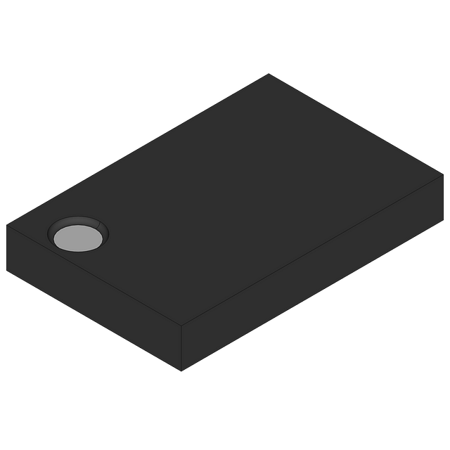
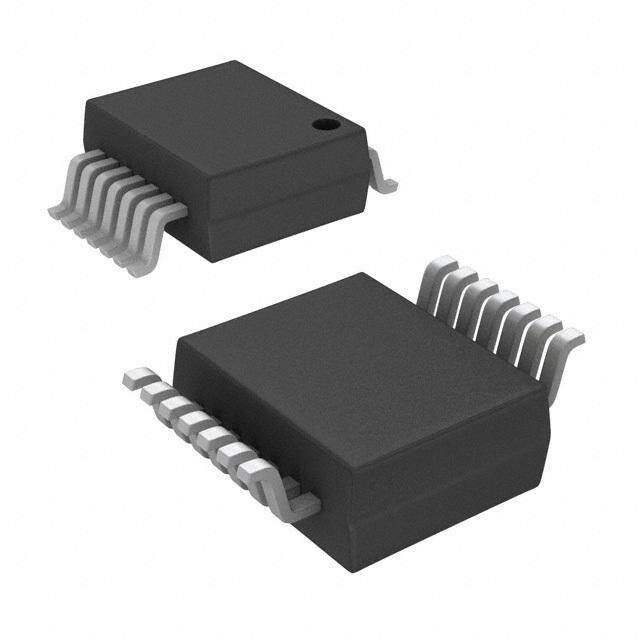
| 产品图片 |
|
| rohs | 符合RoHS无铅 / 符合限制有害物质指令(RoHS)规范要求 |
| 产品系列 | 开关 IC,模拟开关 IC,NXP Semiconductors NX3L1G53GD,125- |
| 数据手册 | |
| 产品型号 | NX3L1G53GD,125 |
| PCN封装 | |
| 产品种类 | 模拟开关 IC |
| 供应商器件封装 | 8-XSON,SOT996-2 (2x3) |
| 其它名称 | 568-5541-2 |
| 功能 | |
| 包装 | 带卷 (TR) |
| 商标 | NXP Semiconductors |
| 安装类型 | 表面贴装 |
| 安装风格 | SMD/SMT |
| 导通电阻 | 500 毫欧 |
| 导通电阻—最大值 | 1.6 Ohms |
| 封装 | Reel |
| 封装/外壳 | 8-XFDFN |
| 封装/箱体 | XSON-8U |
| 工作温度 | -40°C ~ 125°C |
| 工厂包装数量 | 3000 |
| 开关数量 | 1 |
| 开关电流—最大值 | +/- 350 mA, +/- 500 mA |
| 开关配置 | SPDT |
| 最大功率耗散 | 250 mW |
| 最大工作温度 | + 125 C |
| 最小工作温度 | - 40 C |
| 标准包装 | 3,000 |
| 特色产品 | http://www.digikey.com/product-highlights/cn/zh/nxp-semiconductors-micropak/1262 |
| 电压-电源,单/双 (±) | 1.4 V ~ 4.3 V |
| 电压源 | 单电源 |
| 电流-电源 | 150nA |
| 电源电流 | 690 nA, 800 nA |
| 电路 | 1 x SPDT |
| 空闲时间—最大值 | 23 ns |
| 运行时间—最大值 | 50 ns |


PDF Datasheet 数据手册内容提取
NX3L1G53 Low-ohmic single-pole double-throw analog switch Rev. 7.1 — 15 November 2016 Product data sheet 1. General description The NX3L1G53 is a low-ohmic single-pole double-throw analog switch suitable for use as an analog or digital 2:1 multiplexer/demultiplexer. It has a digital select input (S), two independent inputs/outputs (Y0 and Y1), a common input/output (Z) and an active LOW enable input (E). When pin E is HIGH, the switch is turned off. Schmitt trigger action at the digital inputs makes the circuit tolerant to slower input rise and fall times. The NX3L1G53 allows signals with amplitude up to V to be transmitted from Z to Y0 or CC Y1; or from Y0 or Y1 to Z. Its low ON resistance (0.5 ) and flatness (0.13 ) ensures minimal attenuation and distortion of transmitted signals. 2. Features and benefits Wide supply voltage range from 1.4V to 4.3V Very low ON resistance (peak): 1.6 (typical) at V =1.4V CC 1.0 (typical) at V =1.65V CC 0.55 (typical) at V =2.3V CC 0.50 (typical) at V =2.7V CC 0.50 (typical) at V =4.3V CC Break-before-make switching High noise immunity ESD protection: HBM JESD22-A114F Class 3A exceeds 7500V MM JESD22-A115-A exceeds 200V CDM AEC-Q100-011 revision B exceeds 1000V IEC61000-4-2 contact discharge exceeds 8000 V for switch ports CMOS low-power consumption Latch-up performance exceeds 100mA per JESD 78 Class II Level A Direct interface with TTL levels at 3.0 V Control input accepts voltages above supply voltage High current handling capability (350 mA continuous current under 3.3 V supply) Specified from 40C to +85C and from 40C to +125C
NX3L1G53 NXP Semiconductors Low-ohmic single-pole double-throw analog switch 3. Applications Cell phone PDA Portable media player 4. Ordering information Table 1. Ordering info rmation Type number Package Temperature range Name Description Version NX3L1G53GT 40Cto+125C XSON8 plastic extremely thin small outline package; no leads; SOT833-1 8terminals; body 1 1.95 0.5 mm NX3L1G53GD 40Cto+125C XSON8 plastic extremely thin small outline package; noleads; SOT996-2 8terminals; body 3 2 0.5 mm NX3L1G53GM 40C to +125C XQFN8 plastic, extremely thin quad flat package; noleads; SOT902-2 8terminals; body 1.61.60.5mm 5. Marking Table 2. Marking cod es[1] Type number Marking code NX3L1G53GT D53 NX3L1G53GD D53 NX3L1G53GM D53 [1] The pin 1 indicator is located on the lower left corner of the device, below the marking code. 6. Functional diagram 6 Y1 S 5 7 Y0 Z 1 E 2 001aad386 Fig 1. Logic symbol NX3L1G53 All information provided in this document is subject to legal disclaimers. © NXP B.V. 2016. All rights reserved. Product data sheet Rev. 7.1 — 15 November 2016 2 of 24
NX3L1G53 NXP Semiconductors Low-ohmic single-pole double-throw analog switch Y0 S Z Y1 E 001aad387 Fig 2. Logic diagram 7. Pinning information 7.1 Pinning NX3L1G53 Z 1 8 VCC NX3L1G53 E 2 7 Y0 Z 1 8 VCC E 2 7 Y0 GND 3 6 Y1 GND 3 6 Y1 GND 4 5 S GND 4 5 S 001aah454 001aaj534 Transparent top view Transparent top view Fig 3. Pin configuration SOT833-1 (XSON8) Fig 4. Pin configuration SOT996-2 (XSON8) NX3L1G53 All information provided in this document is subject to legal disclaimers. © NXP B.V. 2016. All rights reserved. Product data sheet Rev. 7.1 — 15 November 2016 3 of 24
NX3L1G53 NXP Semiconductors Low-ohmic single-pole double-throw analog switch NX3L1G53 terminal 1 C C index area V Y0 1 8 7 Z Y1 2 6 E S 3 5 GND 4 D GN 001aah455 Transparent top view Fig 5. Pin configuration SOT902-2 (XQFN8) 7.2 Pin description Table 3. Pin descripti on Symbol Pin Description SOT833-1 and SOT996-2 SOT902-2 Z 1 7 common output or input E 2 6 enable input (active LOW) GND 3 5 ground (0V) GND 4 4 ground (0V) S 5 3 select input Y1 6 2 independent input or output Y0 7 1 independent input or output V 8 8 supply voltage CC 8. Functional description Table 4. Function tab le[1] Input Channel S E L L Y0 to Z or Z to Y0 H L Y1 to Z or Z to Y1 X H switch off [1] H=HIGH voltage level; L=LOW voltage level; X=don’t care. NX3L1G53 All information provided in this document is subject to legal disclaimers. © NXP B.V. 2016. All rights reserved. Product data sheet Rev. 7.1 — 15 November 2016 4 of 24
NX3L1G53 NXP Semiconductors Low-ohmic single-pole double-throw analog switch 9. Limiting values Table 5. Limiting valu es In accordance with the Absolute Maximum Rating System (IEC 60134). Voltages are referenced to GND (ground = 0 V). Symbol Parameter Conditions Min Max Unit V supply voltage 0.5 +4.6 V CC V input voltage select input S and enable input E [1] 0.5 +4.6 V I V switch voltage [2] 0.5 V + 0.5 V SW CC I input clamping current V <0.5V 50 - mA IK I I switch clamping current V <0.5V or V >V + 0.5 V - 50 mA SK I I CC I switch current V >0.5V or V < V + 0.5 V; - 350 mA SW SW SW CC sourceorsink current V >0.5V or V < V + 0.5 V; - 500 mA SW SW CC pulsedat1msduration, < 10 % duty cycle; peak current T storage temperature 65 +150 C stg P total power dissipation T =40Cto+125C [3] - 250 mW tot amb [1] The minimum input voltage rating may be exceeded if the input current rating is observed. [2] The minimum and maximum switch voltage ratings may be exceeded if the switch clamping current rating is observed but may not exceed 4.6 V. [3] For XSON8 and XQFN8 packages: above 118C the value of Ptotderates linearly with 7.8mW/K. 10. Recommended operating conditions Table 6. Recommend ed operating conditions Symbol Parameter Conditions Min Max Unit V supply voltage 1.4 4.3 V CC V input voltage select input S and enable input E 0 4.3 V I V switch voltage [1] 0 V V SW CC T ambient temperature 40 +125 C amb t/V input transition rise and fall rate V =1.4Vto4.3V [2] - 200 ns/V CC [1] To avoid sinking GND current from terminal Z when switch current flows in terminal Yn, the voltage drop across the bidirectional switch must not exceed 0.4V. If the switch current flows into terminal Z, noGND current will flow from terminal Yn. In this case, there is no limit for the voltage drop across the switch. [2] Applies to control signals. NX3L1G53 All information provided in this document is subject to legal disclaimers. © NXP B.V. 2016. All rights reserved. Product data sheet Rev. 7.1 — 15 November 2016 5 of 24
NX3L1G53 NXP Semiconductors Low-ohmic single-pole double-throw analog switch 11. Static characteristics Table 7. Static charac teristics At recommended operating conditions; voltages are referenced to GND (ground 0V). Symbol Parameter Conditions 25 C 40 C to +125 C Unit Min Typ Max Min Max Max (85C) (125C) V HIGH-level V =1.4Vto1.95V 0.65V - - 0.65V - - V IH CC CC CC input voltage V =2.3 Vto2.7V 1.7 - - 1.7 - - V CC V =2.7 Vto3.6V 2.0 - - 2.0 - - V CC V =3.6 Vto4.3V 0.7V - - 0.7V - - V CC CC CC V LOW-level V =1.4Vto1.95V - - 0.35V - 0.35V 0.35V V IL CC CC CC CC input voltage V =2.3Vto2.7V - - 0.7 - 0.7 0.7 V CC V =2.7Vto3.6V - - 0.8 - 0.8 0.8 V CC V =3.6 Vto4.3V - - 0.3V - 0.3V 0.3V V CC CC CC CC I input leakage select input S and enable - - - - 0.5 1 A I current inputE; V =GNDto4.3V; I V =1.4Vto4.3V CC I OFF-state Y0 and Y1 port; S(OFF) leakage seeFigure6 current V =1.4Vto3.6V - - 5 - 50 500 nA CC V =3.6Vto4.3V - - 10 - 50 500 nA CC I ON-state Z port; seeFigure7 S(ON) leakage V =1.4Vto3.6V - - 5 - 50 500 nA CC current V =3.6Vto4.3V - - 10 - 50 500 nA CC I supply current V =V orGND; CC I CC V =GNDorV SW CC V =3.6V - - 100 - 690 6000 nA CC V =4.3V - - 150 - 800 7000 nA CC C input - 1.0 - - - - pF I capacitance C OFF-state - 35 - - - - pF S(OFF) capacitance C ON-state - 130 - - - - pF S(ON) capacitance NX3L1G53 All information provided in this document is subject to legal disclaimers. © NXP B.V. 2016. All rights reserved. Product data sheet Rev. 7.1 — 15 November 2016 6 of 24
NX3L1G53 NXP Semiconductors Low-ohmic single-pole double-throw analog switch 11.1 Test circuits VCC switch S E 1 VIL VIH S Y0 1 2 VIH VIH VIL or VIH switch Z Y1 2 IS E GND VIH VI VO 001aad390 VI=0.3VorVCC0.3 V; VO=VCC 0.3 V or 0.3 V. Fig 6. Test circuit for measuring OFF-state leakage current VCC switch S E 1 VIL VIL S Y0 1 2 VIH VIL VIL or VIH switch Z Y1 2 IS E GND VIL VI VO 001aad391 VI=0.3VorVCC0.3 V; VO=open circuit. Fig 7. Test circuit for measuring ON-state leakage current NX3L1G53 All information provided in this document is subject to legal disclaimers. © NXP B.V. 2016. All rights reserved. Product data sheet Rev. 7.1 — 15 November 2016 7 of 24
NX3L1G53 NXP Semiconductors Low-ohmic single-pole double-throw analog switch 11.2 ON resistance Table 8. ON resistanc e At recommended operating conditions; voltages are referenced to GND (ground = 0V); for graphs see Figure9 to Figure15. Symbol Parameter Conditions 40 C to +85 C 40 C to +125 C Unit Min Typ[1] Max Min Max R ON resistance (peak) V =GNDtoV ; ON(peak) I CC I =100mA; SW seeFigure8 V =1.4V - 1.6 3.7 - 4.1 CC V =1.65V - 1.0 1.6 - 1.7 CC V =2.3V - 0.55 0.8 - 0.9 CC V =2.7V - 0.5 0.75 - 0.9 CC V =4.3V - 0.5 0.75 - 0.9 CC R ON resistance mismatch V =GNDtoV ; [2] ON I CC between channels I =100mA SW V =1.4V - 0.04 0.3 - 0.3 CC V =1.65V - 0.04 0.2 - 0.3 CC V =2.3V - 0.02 0.08 - 0.1 CC V =2.7V - 0.02 0.075 - 0.1 CC V =4.3V - 0.02 0.075 - 0.1 CC R ON resistance (flatness) V =GNDtoV ; [3] ON(flat) I CC I =100mA SW V =1.4V - 1.0 3.3 - 3.6 CC V =1.65V - 0.5 1.2 - 1.3 CC V =2.3V - 0.15 0.3 - 0.35 CC V =2.7V - 0.13 0.3 - 0.35 CC V =4.3V - 0.2 0.4 - 0.45 CC [1] Typical values are measured at Tamb=25 C. [2] Measured at identical V , temperature and input voltage. CC [3] Flatness is defined as the difference between the maximum and minimum value of ON resistance measured at identical V and CC temperature. NX3L1G53 All information provided in this document is subject to legal disclaimers. © NXP B.V. 2016. All rights reserved. Product data sheet Rev. 7.1 — 15 November 2016 8 of 24
NX3L1G53 NXP Semiconductors Low-ohmic single-pole double-throw analog switch 11.3 ON resistance test circuit and waveforms V VCC switch S E VSW 1 VIL VIL 2 VIH VIL S Y0 1 VIL or VIH switch Z Y1 2 E VIL GND VI ISW 001aah456 R = V / I . ON SW SW Fig 8. Test circuit for measuring ON resistance 001aag564 1.6 RON (Ω) 1.2 (1) 0.8 (2) (3) 0.4 (4) (5) (6) 0 0 1 2 3 4 5 VI (V) (1) V =1.5V. CC (2) V =1.8V. CC (3) VCC=2.5V. (4) VCC=2.7V. (5) VCC=3.3V. (6) V =4.3V. CC Measured at Tamb=25C. Fig 9. ON resistance as a function of input voltage NX3L1G53 All information provided in this document is subject to legal disclaimers. © NXP B.V. 2016. All rights reserved. Product data sheet Rev. 7.1 — 15 November 2016 9 of 24
NX3L1G53 NXP Semiconductors Low-ohmic single-pole double-throw analog switch 001aag565 001aag566 1.6 1.0 R(ΩO)N R(ΩO)N 0.8 1.2 (1) (2) 0.6 (3) (1) (4) 0.8 (2) (3) (4) 0.4 0.4 0.2 0 0 0 1 2 3 0 1 2 3 VI (V) VI (V) (1) Tamb=125C. (1) Tamb=125C. (2) Tamb=85C. (2) Tamb=85C. (3) Tamb=25C. (3) Tamb=25C. (4) Tamb=40C. (4) Tamb=40C. Fig 10. ON resistance as a function of input voltage; Fig 11. ON resistance as a function of input voltage; V =1.5V V =1.8V CC CC 001aag567 001aaj896 1.0 1.0 RON RON (Ω) (Ω) 0.8 0.8 0.6 (1) 0.6 (1) (2) (2) (3) (3) (4) (4) 0.4 0.4 0.2 0.2 0 0 0 1 2 3 0 1 2 3 4 5 VI (V) VI (V) (1) Tamb=125C. (1) Tamb=125C. (2) Tamb=85C. (2) Tamb=85C. (3) Tamb=25C. (3) Tamb=25C. (4) Tamb=40C. (4) Tamb=40C. Fig 12. ON resistance as a function of input voltage; Fig 13. ON resistance as a function of input voltage; V =2.5V V =2.7V CC CC NX3L1G53 All information provided in this document is subject to legal disclaimers. © NXP B.V. 2016. All rights reserved. Product data sheet Rev. 7.1 — 15 November 2016 10 of 24
NX3L1G53 NXP Semiconductors Low-ohmic single-pole double-throw analog switch 001aag569 001aaj896 1.0 1.0 RON RON (Ω) (Ω) 0.8 0.8 0.6 0.6 (1) (1) (2) (2) (3) (3) (4) 0.4 (4) 0.4 0.2 0.2 0 0 0 1 2 3 4 0 1 2 3 4 5 VI (V) VI (V) (1) Tamb=125C. (1) Tamb=125C. (2) Tamb=85C. (2) Tamb=85C. (3) Tamb=25C. (3) Tamb=25C. (4) Tamb=40C. (4) Tamb=40C. Fig 14. ON resistance as a function of input voltage; Fig 15. ON resistance as a function of input voltage; V =3.3V V =4.3V CC CC 12. Dynamic characteristics Table 9. Dynamic cha racteristics At recommended operating conditions; voltages are referenced to GND (ground=0V); for load circuit see Figure18. Symbol Parameter Conditions 25 C 40 C to +125 C Unit Min Typ[1] Max Min Max Max (85C) (125C) t enable time S or E to Z or Yn; en seeFigure16 V =1.4Vto1.6V - 28 42 - 45 50 ns CC V =1.65Vto1.95V - 23 34 - 37 41 ns CC V =2.3Vto2.7V - 17 27 - 29 31 ns CC V =2.7Vto 3.6V - 15 24 - 26 28 ns CC V =3.6Vto 4.3V - 15 24 - 26 28 ns CC t disable time S or E to Z or Yn; dis seeFigure16 V =1.4Vto1.6V - 10 19 - 21 23 ns CC V =1.65Vto1.95V - 7 14 - 16 17 ns CC V =2.3Vto2.7V - 5 9 - 10 11 ns CC V =2.7Vto 3.6V - 4 8 - 9 9 ns CC V =2.7Vto 4.3V - 4 8 - 9 9 ns CC NX3L1G53 All information provided in this document is subject to legal disclaimers. © NXP B.V. 2016. All rights reserved. Product data sheet Rev. 7.1 — 15 November 2016 11 of 24
NX3L1G53 NXP Semiconductors Low-ohmic single-pole double-throw analog switch Table 9. Dynamic characteristics …continued At recommended operating conditions; voltages are referenced to GND (ground=0V); for load circuit see Figure18. Symbol Parameter Conditions 25 C 40 C to +125 C Unit Min Typ[1] Max Min Max Max (85C) (125C) t break-before-make see Figure17 [2] b-m time V =1.4Vto1.6V - 19 - 9 - - ns CC V =1.65Vto1.95V - 17 - 7 - - ns CC V =2.3Vto2.7V - 13 - 5 - - ns CC V =2.7Vto 3.6V - 10 - 3 - - ns CC V =2.7Vto 4.3V - 10 - 2 - - ns CC [1] Typical values are measured at Tamb=25 C and VCC = 1.5 V, 1.8 V, 2.5 V, 3.3 V and 4.3 V respectively. [2] Break-before-make guaranteed by design. 12.1 Waveform and test circuits VI S, E input VM VM GND ten tdis VOH output VX VX OFF to HIGH HIGH to OFF GND tdis ten VOH output VX VX HIGH to OFF OFF to HIGH GND 001aah457 Measurement points are given in Table10. Logic levels: VOL and VOH are typical output voltage levels that occur with the output load. Fig 16. Enable and disable times Table 10. Measuremen t points Supply voltage Input Output V V V CC M X 1.4V to 4.3V 0.5V 0.9V CC OH NX3L1G53 All information provided in this document is subject to legal disclaimers. © NXP B.V. 2016. All rights reserved. Product data sheet Rev. 7.1 — 15 November 2016 12 of 24
NX3L1G53 NXP Semiconductors Low-ohmic single-pole double-throw analog switch VCC S Y0 Z Y1 E VIL VI G V VO RL CL VEXT = 1.5 V GND 001aah458 a. Test circuit VI 0.5VI 0.9VO 0.9VO VO tb-m 001aag572 b. Input and output measurement points Fig 17. Test circuit for measuring break-before-make timing VCC S Y0 1 switch Z Y1 2 E VIL VI G V VO RL CL VEXT = 1.5 V GND 001aah459 Test data is given in Table11. Definitions test circuit: RL = Load resistance. CL = Load capacitance including jig and probe capacitance. V = External voltage for measuring switching times. EXT VI may be connected to S or E. Fig 18. Test circuit for measuring switching times NX3L1G53 All information provided in this document is subject to legal disclaimers. © NXP B.V. 2016. All rights reserved. Product data sheet Rev. 7.1 — 15 November 2016 13 of 24
NX3L1G53 NXP Semiconductors Low-ohmic single-pole double-throw analog switch Table 11. Test data Supply voltage Input Load V V t, t C R CC I r f L L 1.4V to 4.3V V 2.5ns 35pF 50 CC 12.2 Additional dynamic characteristics Table 12. Additional dy namic characteristics At recommended operating conditions; voltages are referenced to GND (ground=0V); V = GND or V (unless otherwise I CC specified); t =t 2.5ns; T =25C. r f amb Symbol Parameter Conditions Min Typ Max Unit THD total harmonic f =20Hzto20 kHz; R =32; seeFigure19 [1] i L distortion V =1.4V; V =1V(p-p) - 0.15 - % CC I V =1.65V; V =1.2V (p-p) - 0.10 - % CC I V =2.3V; V =1.5V(p-p) - 0.02 - % CC I V =2.7V; V =2V(p-p) - 0.02 - % CC I V =4.3V; V =2V(p-p) - 0.02 - % CC I f 3 dB frequency R =50; seeFigure20 [1] (3dB) L response V =1.4 V to 4.3V - 60 - MHz CC isolation (OFF-state) f =100kHz; R =50; seeFigure21 [1] iso i L V =1.4 V to 4.3V - 90 - dB CC V crosstalk voltage between digital inputs and switch; ct f =1MHz;C =50 pF; R =50; seeFigure22 i L L V =1.4 V to 3.6V - 0.2 - V CC V =3.6 V to 4.3V - 0.3 - V CC Xtalk crosstalk between switches; [1] f =100kHz;R =50;seeFigure23 i L V =1.4 V to 4.3V - 90 - dB CC Q charge injection f =1MHz; C =0.1 nF; R =1 M; V =0V; inj i L L gen R =0; see Figure24 gen V =1.5 V - 3 - pC CC V =1.8 V - 4 - pC CC V =2.5V - 6 - pC CC V =3.3V - 9 - pC CC V =4.3V - 15 - pC CC [1] f is biased at 0.5V . i CC NX3L1G53 All information provided in this document is subject to legal disclaimers. © NXP B.V. 2016. All rights reserved. Product data sheet Rev. 7.1 — 15 November 2016 14 of 24
NX3L1G53 NXP Semiconductors Low-ohmic single-pole double-throw analog switch 12.3 Test circuits VCC 0.5VCC switch S E RL 1 VIL VIL VIL or VIH S Y0 1 switch 2 VIH VIL Z Y1 2 E VIL fi D GND 001aah460 Fig 19. Test circuit for measuring total harmonic distortion VCC 0.5VCC switch S E RL 1 VIL VIL VIL or VIH S Y0 1 switch 2 VIH VIL Z Y1 2 E VIL fi dB GND 001aah461 Adjust fi voltage to obtain 0dBm level at output. Increase fi frequency until dB meter reads 3dB. Fig 20. Test circuit for measuring the frequency response when switch is in ON-state 0.5VCC VCC 0.5VCC switch S E RL RL 1 VIH VIH VIL or VIH S Y0 1 switch 2 VIL VIH Z Y1 2 E VIH fi dB GND 001aah462 Adjust f voltage to obtain 0dBm level at input. i Fig 21. Test circuit for measuring isolation (OFF-state) NX3L1G53 All information provided in this document is subject to legal disclaimers. © NXP B.V. 2016. All rights reserved. Product data sheet Rev. 7.1 — 15 November 2016 15 of 24
NX3L1G53 NXP Semiconductors Low-ohmic single-pole double-throw analog switch VCC E S Y0 VIL or VIH Z Y1 VI G liongpiuct RL RL CL V VO 0.5VCC 0.5VCC 001aah452 a. Test circuit logic input (S, E) off on off VO Vct 001aah453 b. Input and output pulse definitions V may be connected to S or E. I Fig 22. Test circuit for measuring crosstalk voltage between digital inputs and switch VCC 0.5VCC 0.5VCC RL RL S Y0 1 VIL or VIH Z Y1 2 E VIH fi dB GND 001aah463 Fig 23. Test circuit for measuring crosstalk NX3L1G53 All information provided in this document is subject to legal disclaimers. © NXP B.V. 2016. All rights reserved. Product data sheet Rev. 7.1 — 15 November 2016 16 of 24
NX3L1G53 NXP Semiconductors Low-ohmic single-pole double-throw analog switch VCC S Y0 1 switch Z Y1 2 E VIL Rgen G VI VO RL CL Vgen GND 001aad398 a. Test circuit logic input off on off (S, E) VO ΔVO 001aah451 b. Input and output pulse definitions Qinj=VO CL. VO = output voltage variation. Rgen = generator resistance. V = generator voltage. gen VI may be connected to S or E. Fig 24. Test circuit for measuring charge injection NX3L1G53 All information provided in this document is subject to legal disclaimers. © NXP B.V. 2016. All rights reserved. Product data sheet Rev. 7.1 — 15 November 2016 17 of 24
NX3L1G53 NXP Semiconductors Low-ohmic single-pole double-throw analog switch 13. Package outline XSON8: plastic extremely thin small outline package; no leads; 8 terminals; body 1 x 1.95 x 0.5 mm SOT833-1 b 1 2 3 4 4× L1 L (2) e 8 7 6 5 e1 e1 e1 8× A (2) A1 D E terminal 1 index area 0 1 2 mm scale DIMENSIONS (mm are the original dimensions) UNIT mA(a1x) mAa1x b D E e e1 L L1 0.25 2.0 1.05 0.35 0.40 mm 0.5 0.04 0.6 0.5 0.17 1.9 0.95 0.27 0.32 Notes 1. Including plating thickness. 2. Can be visible in some manufacturing processes. OUTLINE REFERENCES EUROPEAN ISSUE DATE VERSION IEC JEDEC JEITA PROJECTION 07-11-14 SOT833-1 - - - MO-252 - - - 07-12-07 Fig 25. Package outline SOT833-1 (XSON8) NX3L1G53 All information provided in this document is subject to legal disclaimers. © NXP B.V. 2016. All rights reserved. Product data sheet Rev. 7.1 — 15 November 2016 18 of 24
NX3L1G53 NXP Semiconductors Low-ohmic single-pole double-throw analog switch XSON8: plastic extremely thin small outline package; no leads; 8 terminals; body 3 x 2 x 0.5 mm SOT996-2 D B A E A A1 detail X terminal 1 index area e1 C v C A B L1 e b w C y1C y 1 4 L2 L 8 5 X 0 1 2 mm scale Dimensions (mm are the original dimensions) Unit(1) A A1 b D E e e1 L L1 L2 v w y y1 max 0.05 0.35 2.1 3.1 0.5 0.15 0.6 mm nom 0.5 0.5 1.5 0.1 0.05 0.05 0.1 min 0.00 0.15 1.9 2.9 0.3 0.05 0.4 sot996-2_po Outline References European Issue date version IEC JEDEC JEITA projection 07-12-21 SOT996-2 12-11-20 Fig 26. Package outline SOT996-2 (XSON8) NX3L1G53 All information provided in this document is subject to legal disclaimers. © NXP B.V. 2016. All rights reserved. Product data sheet Rev. 7.1 — 15 November 2016 19 of 24
NX3L1G53 NXP Semiconductors Low-ohmic single-pole double-throw analog switch XQFN8: plastic, extremely thin quad flat package; no leads; 8 terminals; body 1.6 x 1.6 x 0.5 mm SOT902-2 X D B A terminal 1 index area E A A1 detail X e C v C A B b w C y1C y 4 3 5 e1 terminal 1 index area 2 6 k L 1 7 8 metal area L2 not for soldering L k L3 L1 0 1 2 mm scale Dimensions Unit(1) A A1 b D E e e1 k L L1 L2 L3 v w y y1 max 0.5 0.05 0.25 1.65 1.65 0.35 0.15 0.25 0.35 mm nom 0.20 1.60 1.60 0.55 0.5 0.30 0.10 0.20 0.30 0.1 0.05 0.05 0.05 min 0.00 0.15 1.55 1.55 0.2 0.25 0.05 0.15 0.25 Note 1. Plastic or metal protrusions of 0.075 mm maximum per side are not included. sot902-2_po Outline References European Issue date version IEC JEDEC JEITA projection 16-07-14 SOT902-2 - - - MO-255 - - - 16-11-08 Fig 27. Package outline SOT902-2 (XQFN8) NX3L1G53 All information provided in this document is subject to legal disclaimers. © NXP B.V. 2016. All rights reserved. Product data sheet Rev. 7.1 — 15 November 2016 20 of 24
NX3L1G53 NXP Semiconductors Low-ohmic single-pole double-throw analog switch 14. Abbreviations Table 13. Abbreviation s Acronym Description CDM Charged Device Model CMOS Complementary Metal Oxide Semiconductor ESD ElectroStatic Discharge HBM Human Body Model MM Machine Model TTL Transistor-Transistor Logic 15. Revision history T able 14. Revision history Document ID Release date Data sheet status Change notice Supersedes NX3L1G53 v.7.1 20161115 Product data sheet - NX3L1G53 v.7 Modifications: • Updated Figure 27 “Package outline SOT902-2 (XQFN8)” NX3L1G53 v.7 20130208 Product data sheet - NX3L1G53 v.6 Modifications: • For type number NX3L1G53GD XSON8U has changed to XSON8 NX3L1G53 v.6 20120613 Product data sheet - NX3L1G53 v.5 NX3L1G53 v.5 20111109 Product data sheet - NX3L1G53 v.4 NX3L1G53 v.4 20100127 Product data sheet - NX3L1G53 v.3 NX3L1G53 v.3 20090417 Product data sheet - NX3L1G53 v.2 NX3L1G53 v.2 20080718 Product data sheet - NX3L1G53 v.1 NX3L1G53 v.1 20080408 Product data sheet - - NX3L1G53 All information provided in this document is subject to legal disclaimers. © NXP B.V. 2016. All rights reserved. Product data sheet Rev. 7.1 — 15 November 2016 21 of 24
NX3L1G53 NXP Semiconductors Low-ohmic single-pole double-throw analog switch 16. Legal information 16.1 Data sheet status Document status[1][2] Product status[3] Definition Objective [short] data sheet Development This document contains data from the objective specification for product development. Preliminary [short] data sheet Qualification This document contains data from the preliminary specification. Product [short] data sheet Production This document contains the product specification. [1] Please consult the most recently issued document before initiating or completing a design. [2] The term ‘short data sheet’ is explained in section “Definitions”. [3] The product status of device(s) described in this document may have changed since this document was published and may differ in case of multiple devices. The latest product status information is available on the Internet at URLhttp://www.nxp.com. 16.2 Definitions Suitability for use — NXP Semiconductors products are not designed, authorized or warranted to be suitable for use in life support, life-critical or safety-critical systems or equipment, nor in applications where failure or Draft — The document is a draft version only. The content is still under malfunction of an NXP Semiconductors product can reasonably be expected internal review and subject to formal approval, which may result in to result in personal injury, death or severe property or environmental modifications or additions. NXP Semiconductors does not give any damage. NXP Semiconductors and its suppliers accept no liability for representations or warranties as to the accuracy or completeness of inclusion and/or use of NXP Semiconductors products in such equipment or information included herein and shall have no liability for the consequences of applications and therefore such inclusion and/or use is at the customer’s own use of such information. risk. Short data sheet — A short data sheet is an extract from a full data sheet Applications — Applications that are described herein for any of these with the same product type number(s) and title. A short data sheet is intended products are for illustrative purposes only. NXP Semiconductors makes no for quick reference only and should not be relied upon to contain detailed and representation or warranty that such applications will be suitable for the full information. For detailed and full information see the relevant full data specified use without further testing or modification. sheet, which is available on request via the local NXP Semiconductors sales office. In case of any inconsistency or conflict with the short data sheet, the Customers are responsible for the design and operation of their applications full data sheet shall prevail. and products using NXP Semiconductors products, and NXP Semiconductors accepts no liability for any assistance with applications or customer product Product specification — The information and data provided in a Product design. It is customer’s sole responsibility to determine whether the NXP data sheet shall define the specification of the product as agreed between Semiconductors product is suitable and fit for the customer’s applications and NXP Semiconductors and its customer, unless NXP Semiconductors and products planned, as well as for the planned application and use of customer have explicitly agreed otherwise in writing. In no event however, customer’s third party customer(s). Customers should provide appropriate shall an agreement be valid in which the NXP Semiconductors product is design and operating safeguards to minimize the risks associated with their deemed to offer functions and qualities beyond those described in the applications and products. Product data sheet. NXP Semiconductors does not accept any liability related to any default, damage, costs or problem which is based on any weakness or default in the 16.3 Disclaimers customer’s applications or products, or the application or use by customer’s third party customer(s). Customer is responsible for doing all necessary testing for the customer’s applications and products using NXP Limited warranty and liability — Information in this document is believed to Semiconductors products in order to avoid a default of the applications and be accurate and reliable. However, NXP Semiconductors does not give any the products or of the application or use by customer’s third party representations or warranties, expressed or implied, as to the accuracy or customer(s). NXP does not accept any liability in this respect. completeness of such information and shall have no liability for the consequences of use of such information. NXP Semiconductors takes no Limiting values — Stress above one or more limiting values (as defined in responsibility for the content in this document if provided by an information the Absolute Maximum Ratings System of IEC60134) will cause permanent source outside of NXP Semiconductors. damage to the device. Limiting values are stress ratings only and (proper) operation of the device at these or any other conditions above those given in In no event shall NXP Semiconductors be liable for any indirect, incidental, the Recommended operating conditions section (if present) or the punitive, special or consequential damages (including - without limitation - lost Characteristics sections of this document is not warranted. Constant or profits, lost savings, business interruption, costs related to the removal or repeated exposure to limiting values will permanently and irreversibly affect replacement of any products or rework charges) whether or not such the quality and reliability of the device. damages are based on tort (including negligence), warranty, breach of contract or any other legal theory. Terms and conditions of commercial sale — NXP Semiconductors products are sold subject to the general terms and conditions of commercial Notwithstanding any damages that customer might incur for any reason whatsoever, NXP Semiconductors’ aggregate and cumulative liability towards sale, as published at http://www.nxp.com/profile/terms, unless otherwise customer for the products described herein shall be limited in accordance agreed in a valid written individual agreement. In case an individual with the Terms and conditions of commercial sale of NXP Semiconductors. agreement is concluded only the terms and conditions of the respective agreement shall apply. NXP Semiconductors hereby expressly objects to Right to make changes — NXP Semiconductors reserves the right to make applying the customer’s general terms and conditions with regard to the changes to information published in this document, including without purchase of NXP Semiconductors products by customer. limitation specifications and product descriptions, at any time and without notice. This document supersedes and replaces all information supplied prior No offer to sell or license — Nothing in this document may be interpreted or to the publication hereof. construed as an offer to sell products that is open for acceptance or the grant, conveyance or implication of any license under any copyrights, patents or other industrial or intellectual property rights. NX3L1G53 All information provided in this document is subject to legal disclaimers. © NXP B.V. 2016. All rights reserved. Product data sheet Rev. 7.1 — 15 November 2016 22 of 24
NX3L1G53 NXP Semiconductors Low-ohmic single-pole double-throw analog switch Export control — This document as well as the item(s) described herein NXP Semiconductors’ specifications such use shall be solely at customer’s may be subject to export control regulations. Export might require a prior own risk, and (c) customer fully indemnifies NXP Semiconductors for any authorization from competent authorities. liability, damages or failed product claims resulting from customer design and use of the product for automotive applications beyond NXP Semiconductors’ Non-automotive qualified products — Unless this data sheet expressly standard warranty and NXP Semiconductors’ product specifications. states that this specific NXP Semiconductors product is automotive qualified, the product is not suitable for automotive use. It is neither qualified nor tested Translations — A non-English (translated) version of a document is for in accordance with automotive testing or application requirements. NXP reference only. The English version shall prevail in case of any discrepancy Semiconductors accepts no liability for inclusion and/or use of between the translated and English versions. non-automotive qualified products in automotive equipment or applications. In the event that customer uses the product for design-in and use in 16.4 Trademarks automotive applications to automotive specifications and standards, customer (a) shall use the product without NXP Semiconductors’ warranty of the Notice: All referenced brands, product names, service names and trademarks product for such automotive applications, use and specifications, and (b) are the property of their respective owners. whenever customer uses the product for automotive applications beyond 17. Contact information For more information, please visit: http://www.nxp.com For sales office addresses, please send an email to: salesaddresses@nxp.com NX3L1G53 All information provided in this document is subject to legal disclaimers. © NXP B.V. 2016. All rights reserved. Product data sheet Rev. 7.1 — 15 November 2016 23 of 24
NX3L1G53 NXP Semiconductors Low-ohmic single-pole double-throw analog switch 18. Contents 1 General description. . . . . . . . . . . . . . . . . . . . . . 1 2 Features and benefits . . . . . . . . . . . . . . . . . . . . 1 3 Applications. . . . . . . . . . . . . . . . . . . . . . . . . . . . 2 4 Ordering information. . . . . . . . . . . . . . . . . . . . . 2 5 Marking. . . . . . . . . . . . . . . . . . . . . . . . . . . . . . . . 2 6 Functional diagram . . . . . . . . . . . . . . . . . . . . . . 2 7 Pinning information. . . . . . . . . . . . . . . . . . . . . . 3 7.1 Pinning . . . . . . . . . . . . . . . . . . . . . . . . . . . . . . . 3 7.2 Pin description . . . . . . . . . . . . . . . . . . . . . . . . . 4 8 Functional description . . . . . . . . . . . . . . . . . . . 4 9 Limiting values. . . . . . . . . . . . . . . . . . . . . . . . . . 5 10 Recommended operating conditions. . . . . . . . 5 11 Static characteristics. . . . . . . . . . . . . . . . . . . . . 6 11.1 Test circuits. . . . . . . . . . . . . . . . . . . . . . . . . . . . 7 11.2 ON resistance. . . . . . . . . . . . . . . . . . . . . . . . . . 8 11.3 ON resistance test circuit and waveforms . . . . 9 12 Dynamic characteristics. . . . . . . . . . . . . . . . . 11 12.1 Waveform and test circuits. . . . . . . . . . . . . . . 12 12.2 Additional dynamic characteristics . . . . . . . . . 14 12.3 Test circuits. . . . . . . . . . . . . . . . . . . . . . . . . . . 15 13 Package outline. . . . . . . . . . . . . . . . . . . . . . . . 18 14 Abbreviations. . . . . . . . . . . . . . . . . . . . . . . . . . 21 15 Revision history. . . . . . . . . . . . . . . . . . . . . . . . 21 16 Legal information. . . . . . . . . . . . . . . . . . . . . . . 22 16.1 Data sheet status . . . . . . . . . . . . . . . . . . . . . . 22 16.2 Definitions. . . . . . . . . . . . . . . . . . . . . . . . . . . . 22 16.3 Disclaimers. . . . . . . . . . . . . . . . . . . . . . . . . . . 22 16.4 Trademarks. . . . . . . . . . . . . . . . . . . . . . . . . . . 23 17 Contact information. . . . . . . . . . . . . . . . . . . . . 23 18 Contents. . . . . . . . . . . . . . . . . . . . . . . . . . . . . . 24 Please be aware that important notices concerning this document and the product(s) described herein, have been included in section ‘Legal information’. © NXP B.V. 2016. All rights reserved. For more information, please visit: http://www.nxp.com For sales office addresses, please send an email to: salesaddresses@nxp.com Date of release: 15 November 2016 Document identifier: NX3L1G53