ICGOO在线商城 > 集成电路(IC) > 逻辑 - 缓冲器,驱动器,接收器,收发器 > NL27WZ16DFT2G
 Datasheet下载
- 型号: NL27WZ16DFT2G
- 制造商: ON Semiconductor
- 库位|库存: xxxx|xxxx
- 要求:
| 数量阶梯 | 香港交货 | 国内含税 |
| +xxxx | $xxxx | ¥xxxx |
查看当月历史价格
查看今年历史价格
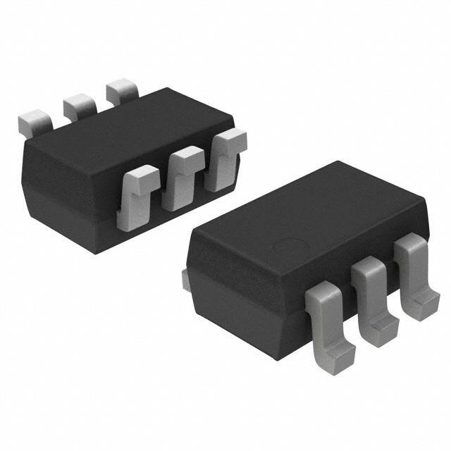
NL27WZ16DFT2G产品简介:
ICGOO电子元器件商城为您提供NL27WZ16DFT2G由ON Semiconductor设计生产,在icgoo商城现货销售,并且可以通过原厂、代理商等渠道进行代购。 NL27WZ16DFT2G价格参考。ON SemiconductorNL27WZ16DFT2G封装/规格:逻辑 - 缓冲器,驱动器,接收器,收发器, Buffer, Non-Inverting 2 Element 1 Bit per Element Push-Pull Output SC-88/SC70-6/SOT-363。您可以下载NL27WZ16DFT2G参考资料、Datasheet数据手册功能说明书,资料中有NL27WZ16DFT2G 详细功能的应用电路图电压和使用方法及教程。
ON Semiconductor的NL27WZ16DFT2G是一款低电压、低功耗的双通道反相缓冲器/驱动器,属于逻辑器件中的缓冲器类别。该器件采用先进的CMOS技术制造,工作电压范围宽(1.65V至5.5V),适用于多种电源环境,具备良好的电平转换能力。

NL27WZ16DFT2G常用于需要信号整形与增强的应用场景,例如便携式消费电子产品(如智能手机、平板电脑)、通信设备、工业控制模块以及电池供电系统。其高输出驱动能力使其适合驱动中等负载的信号线路,广泛应用于数据总线驱动、地址锁存、时钟信号缓冲和接口电平转换等场合。

由于其采用SOT-363(SC-88)小型封装,节省PCB空间,特别适用于对尺寸要求严格的高密度电路设计。此外,该器件具有高噪声抑制能力和稳定的输出特性,可在较宽的温度范围(-40°C 至 +85°C)内可靠工作,适用于工业级应用环境。

NL27WZ16DFT2G还具备低静态功耗和快速响应时间,有助于提升系统能效,延长电池寿命,因此在移动设备和嵌入式系统中广泛应用。总体而言,该器件是一款高性能、多功能的逻辑缓冲器,适用于各类需要信号隔离、驱动增强和电平兼容的数字电路系统。
| 参数 | 数值 |
| 产品目录 | 集成电路 (IC)半导体 |
| 描述 | IC BUFFER DUAL NON-INVERT SC88缓冲器和线路驱动器 1.65-5.5V Dual |
| 产品分类 | |
| 品牌 | ON Semiconductor |
| 产品手册 | |
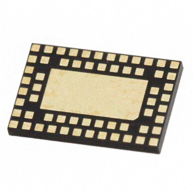
| 产品图片 |
|
| rohs | 符合RoHS无铅 / 符合限制有害物质指令(RoHS)规范要求 |
| 产品系列 | 逻辑集成电路,缓冲器和线路驱动器,ON Semiconductor NL27WZ16DFT2G27WZ |
| 数据手册 | |
| 产品型号 | NL27WZ16DFT2G |
| PCN设计/规格 | |
| 产品目录页面 | |
| 产品种类 | 缓冲器和线路驱动器 |
| 传播延迟时间 | 4.6 ns at 3.3 V, 3.8 ns at 5 V |
| 低电平输出电流 | 32 mA |
| 供应商器件封装 | SC-88/SC70-6/SOT-363 |
| 元件数 | 2 |
| 其它名称 | NL27WZ16DFT2GOSCT |
| 包装 | 剪切带 (CT) |
| 商标 | ON Semiconductor |
| 安装类型 | 表面贴装 |
| 安装风格 | SMD/SMT |
| 封装 | Reel |
| 封装/外壳 | 6-TSSOP,SC-88,SOT-363 |
| 封装/箱体 | SC-70-6 |
| 工作温度 | -55°C ~ 125°C |
| 工厂包装数量 | 3000 |
| 最大功率耗散 | 200 mW |
| 最大工作温度 | + 85 C |
| 最小工作温度 | - 40 C |
| 极性 | Non-Inverting |
| 标准包装 | 1 |
| 每元件位数 | 1 |
| 每芯片的通道数量 | 2 |
| 电压-电源 | 1.65 V ~ 5.5 V |
| 电流-输出高,低 | 32mA,32mA |
| 电源电压-最大 | 5.5 V |
| 电源电压-最小 | 1.65 V |
| 系列 | NL27WZ16 |
| 输入线路数量 | 2 |
| 输出线路数量 | 2 |
| 逻辑类型 | CMOS |
| 逻辑系列 | LCX |
| 高电平输出电流 | - 32 mA |


- 商务部:美国ITC正式对集成电路等产品启动337调查
- 曝三星4nm工艺存在良率问题 高通将骁龙8 Gen1或转产台积电
- 太阳诱电将投资9.5亿元在常州建新厂生产MLCC 预计2023年完工
- 英特尔发布欧洲新工厂建设计划 深化IDM 2.0 战略
- 台积电先进制程称霸业界 有大客户加持明年业绩稳了
- 达到5530亿美元!SIA预计今年全球半导体销售额将创下新高
- 英特尔拟将自动驾驶子公司Mobileye上市 估值或超500亿美元
- 三星加码芯片和SET,合并消费电子和移动部门,撤换高东真等 CEO
- 三星电子宣布重大人事变动 还合并消费电子和移动部门
- 海关总署:前11个月进口集成电路产品价值2.52万亿元 增长14.8%


PDF Datasheet 数据手册内容提取
NL27WZ16 Dual Buffer The NL27WZ16 is a high performance dual buffer operating from a 1.65 to 5.5 V supply. At V = 3 V, high impedance TTL compatible CC inputs significantly reduce current loading to input drivers while TTL compatible outputs offer improved switching noise performance. Features http://onsemi.com • Extremely High Speed: t 2.0 ns (typical) at V = 5 V PD CC • MARKING Designed for 1.65 V to 5.5 V V Operation CC DIAGRAMS • Over Voltage Tolerant Inputs • LVTTL Compatible − Interface Capability With 5 V TTL Logic with VCC = 3 V SC−88/SC−70−6/SOT−363 MMR M(cid:2) • DF SUFFIX (cid:2) LVCMOS Compatible 1 CASE 419B • 1 24 mA Balanced Output Sink and Source Capability • Near Zero Static Supply Current Substantially Reduces System Power Requirements • TSOP−6 Chip Complexity: FET = 72; Equivalent Gate = 18 MR M(cid:2) DT SUFFIX • (cid:2) These Devices are Pb−Free and are RoHS Compliant 1 CASE 318G • NLV Prefix for Automotive and Other Applications Requiring 1 Unique Site and Control Change Requirements; AEC−Q100 Qualified and PPAP Capable MR = Device Code M = Date Code* (cid:2) = Pb−Free Package (Note: Microdot may be in either location) IN A1 1 6 OUT Y1 *Date Code orientation and/or position may vary depending upon manufacturing location. GND 2 5 VCC PIN ASSIGNMENT Pin Function IN A2 3 4 OUT Y2 1 IN A1 2 GND 3 IN A2 Figure 1. Pinout (Top View) 4 OUT Y2 5 VCC 6 OUT Y1 IN A1 1 OUT Y1 FUNCTION TABLE IN A2 1 OUT Y2 A Input Y Output L L Figure 2. Logic Symbol H H ORDERING INFORMATION See detailed ordering and shipping information in the package dimensions section on page 4 of this data sheet. © Semiconductor Components Industries, LLC, 2012 1 Publication Order Number: May, 2012 − Rev. 9 NL27WZ16/D
NL27WZ16 MAXIMUM RATINGS Symbol Characteristics Value Units VCC DC Supply Voltage −0.5 to +7.0 V VI DC Input Voltage −0.5 ≤ VI ≤ +7.0 V VO DC Output Voltage −0.5 ≤ VO ≤ +7.0 V Output in Z or LOW State (Note 1) IIK DC Input Diode Current −50 mA VI < GND IOK DC Output Diode Current −50 mA VO < GND IO DC Output Sink Current ±50 mA ICC DC Supply Current per Supply Pin ±100 mA IGND DC Ground Current per Ground Pin ±100 mA TSTG Storage Temperature Range −65 to +150 °C PD Power Dissipation in Still Air mW SC−88, TSOP−6 200 (cid:2)JA Thermal Resistance °C/W SC−88, TSOP−6 333 TL Lead Temperature, 1 mm from Case for 10 Seconds 260 °C TJ Junction Temperature Under Bias +150 °C VESD ESD Withstand Voltage V Human Body Model (Note 2) > 2000 Machine Model (Note 3) > 200 Charged Device Model (Note 4) N/A ILatchup Latchup Performance mA Above VCC and Below GND at 85°C (Note 5) ±500 Stresses exceeding Maximum Ratings may damage the device. Maximum Ratings are stress ratings only. Functional operation above the Recommended Operating Conditions is not implied. Extended exposure to stresses above the Recommended Operating Conditions may affect device reliability. 1. IO absolute maximum rating must be observed. 2. Tested to EIA/JESD22−A114−A 3. Tested to EIA/JESD22−A115−A 4. Tested to JESD22−C101−A 5. Tested to EIA/JESD78 RECOMMENDED OPERATING CONDITIONS Symbol Parameter Min Max Units VCC Supply Voltage V Operating 1.65 5.5 Data Retention Only 1.5 5.5 VI Input Voltage 0 5.5 V VO Output Voltage (High or LOW State) 0 5.5 V TA Operating Free−Air Temperature −55 +125 °C (cid:3)t/(cid:3)V Input Transition Rise or Fall Rate ns/V VCC = 1.8 V ±0.15 V 0 20 VCC = 2.5 V ±0.2 V 0 20 VCC = 3.0 V ±0.3 V 0 10 VCC = 5.0 V ±0.5 V 0 5 http://onsemi.com 2
NL27WZ16 DC ELECTRICAL CHARACTERISTICS VCC TA = 25(cid:2)C −55(cid:2)C (cid:3) TA (cid:3) 125(cid:2)C Symbol Parameter Condition (V) Min Typ Max Min Max Units VIH High−Level Input 1.65 to 1.95 0.75 VCC 0.75 VCC Voltage 2.3 to 5.5 0.7 VCC 0.7 VCC V VIL Low−Level Input 1.65 to 1.95 0.25 VCC 0.25 VCC Voltage 2.3 to 5.5 0.3 VCC 0.3 VCC V VOH High−Level Output IOH = −100 (cid:4)A 1.65 1.55 1.65 1.55 Voltage 1.8 1.7 1.8 1.7 V VIN = VIH 2.3 2.2 2.3 2.2 3.0 2.9 3.0 2.9 4.5 4.4 4.5 4.4 IOH = −4 mA 1.65 1.29 1.52 1.29 IOH = −8 mA 2.3 1.9 2.15 1.9 V IOH = −16 mA 3.0 2.4 2.80 2.4 IOH = −24 mA 3.0 2.3 2.68 2.3 IOH = −32 mA 4.5 3.8 4.20 3.8 VOL Low−Level Output IOL = 100 (cid:4)A 1.65 0.0 0.1 0.1 Voltage 1.8 0.0 0.1 0.1 V VIN = VIL 2.3 0.0 0.1 0.1 3.0 0.0 0.1 0.1 4.5 0.0 0.1 0.1 IOL = 4 mA 1.65 0.08 0.24 0.24 IOL = 8 mA 2.3 0.10 0.30 0.30 V IOL = 16 mA 3.0 0.15 0.40 0.40 IOL = 24 mA 3.0 0.22 0.55 0.55 IOL = 32 mA 4.5 0.22 0.55 0.55 IIN Input Leakage Current VIN = 5.5 V or GND 0 to 5.5 ±0.1 ±1.0 (cid:4)A IOFF Power Off Leakage VIN = 5.5 V or 0 1 10 Current VOUT = 5.5 V (cid:4)A ICC Quiescent Supply VIN = 5.5 V or GND 5.5 1 10 (cid:4)A Current ÎÎÎÎÎÎÎÎÎÎÎÎÎÎÎÎÎÎÎÎÎÎÎÎÎÎÎÎÎÎÎÎÎ AC ELECTRICAL CHARACTERISTICS tR = tF = 2.5 ns; CL = 50 pF; RL = 500 (cid:5) ÎÎÎÎÎÎÎÎÎÎÎÎÎÎÎÎÎÎÎÎÎÎÎÎÎÎÎÎÎÎÎÎÎÎÎÎÎÎÎÎÎÎÎÎÎÎÎÎÎÎÎÎÎÎÎÎÎÎÎÎÎÎÎÎÎÎÎÎÎÎÎ TA = 25°C −55°C (cid:3) TA (cid:3) 125°C ÎÎÎÎÎÎÎÎÎÎÎÎÎÎÎÎÎÎÎÎÎÎÎÎÎÎÎÎÎÎÎÎÎÎÎÎÎÎÎÎÎÎÎÎÎÎÎÎÎÎÎÎÎÎÎ Symbol Parameter Condition VCC (V) Min Typ Max Min Max Units ÎÎÎÎÎÎÎÎÎÎÎÎÎÎÎÎÎÎÎÎÎÎÎÎÎÎÎÎÎÎÎÎÎÎÎÎÎÎÎÎÎÎÎÎÎÎÎÎÎÎÎÎÎÎÎÎÎÎÎÎÎÎÎÎÎÎÎÎÎÎÎÎÎÎÎÎÎÎÎÎÎÎ tPLH Propagation Delay RL = 1 M(cid:5)(cid:6) CL = 15 pF 1.8 ±0.15 1.8 8.0 9.6 1.8 10.2 ns ÎÎtPÎHL ÎÎ(FÎigurÎe 3 aÎnd 4Î) ÎÎÎÎÎRL ÎÎ= 1 MÎÎ(cid:5)(cid:6) ÎÎCL =ÎÎ 15 pÎÎÎÎF ÎÎ2.ÎÎ5 ±0ÎÎ.2 ÎÎÎÎÎÎ1.0ÎÎÎÎÎÎ3.0ÎÎÎÎÎÎ5.ÎÎ2 ÎÎÎÎÎÎ1.0ÎÎÎÎÎÎÎÎ5.8ÎÎÎÎ ÎÎÎÎÎÎÎÎÎÎÎÎÎÎÎÎÎÎÎÎÎÎÎÎÎÎÎÎÎÎÎÎÎÎÎÎÎÎÎÎÎÎÎÎÎÎÎÎÎÎÎÎÎÎÎÎÎÎÎÎÎÎÎÎÎÎÎÎÎÎ RL = 1 M(cid:5)(cid:6) CL = 15 pF 0.8 2.3 3.6 0.8 4.0 ÎÎÎÎÎÎÎÎÎÎÎÎÎÎÎÎÎÎÎÎÎÎÎÎÎÎ3.Î3 ±0Î.3 ÎÎÎÎÎÎÎÎÎÎÎÎÎÎÎÎÎÎÎÎÎÎÎÎÎÎÎÎÎÎÎÎÎÎÎÎÎ RL = 500 (cid:5)(cid:6) CL = 50 pF 1.2 3.0 4.6 1.2 5.1 ÎÎÎÎÎÎÎÎÎÎÎÎÎÎÎÎÎÎÎÎÎÎÎÎÎÎÎÎÎÎÎÎÎÎÎÎÎÎÎÎÎÎÎÎÎÎÎÎÎÎÎÎÎÎÎÎÎÎÎÎÎÎÎÎÎÎÎÎÎÎ RL = 1 M(cid:5)(cid:6) CL = 15 pF 0.5 1.8 2.9 0.5 3.2 ÎÎÎÎÎÎÎÎÎÎÎÎÎÎÎÎÎÎÎÎÎÎÎÎÎÎ5.Î0 ±0Î.5 ÎÎÎÎÎÎÎÎÎÎÎÎÎÎÎÎÎÎÎÎÎÎÎÎÎÎÎÎÎÎÎÎÎÎÎÎÎ RL = 500 (cid:5)(cid:6) CL = 50 pF 0.8 2.4 3.8 0.8 4.2 ÎÎÎÎÎÎÎÎÎÎÎÎÎÎÎÎÎÎÎÎÎÎÎÎÎÎÎÎÎÎÎÎÎÎÎÎÎÎÎÎÎ CAPACITIVE CHARACTERISTICS Symbol Parameter Condition Typical Units CIN Input Capacitance VCC = 5.5 V, VI = 0 V or VCC 7.0 pF CPD Power Dissipation Capacitance (Note 6) 10 MHz, VCC = 3.3 V, VI = 0 V or VCC 9 pF 10 MHz, VCC = 5.5 V, VI = 0 V or VCC 11 6. CPD is defined as the value of the internal equivalent capacitance which is calculated from the operating current consumption without load. Average operating current can be obtained by the equation: ICC(OPR) = CPD (cid:2) VCC (cid:2) fin (cid:2) ICC. CPD is used to determine the no−load dynamic power consumption; PD = CPD (cid:2) VCC2 (cid:2) fin (cid:2) ICC (cid:2) VCC. http://onsemi.com 3
NL27WZ16 A VCC 50% GND tPLH tPHL Y 50% VCC PROPAGATION DELAYS tR = tF = 2.5 ns, 10% to 90%; f = 1 MHz; tW = 500 ns Figure 3. Switching Waveforms VCC PULSE DUT GENERATOR RT CL RL RT = ZOUT of pulse generator (typically 50 (cid:5)) Figure 4. Test Circuit ORDERING INFORMATION Device Package Shipping† NL27WZ16DFT2G SC−88/SC−70/SOT−363 3000 /Tape & Reel (Pb−Free) NLV27WZ16DFT2G* SC−88/SC−70/SOT−363 3000 /Tape & Reel (Pb−Free) NL27WZ16DTT1G TSOP−6 3000 /Tape & Reel (Pb−Free) †For information on tape and reel specifications, including part orientation and tape sizes, please refer to our Tape and Reel Packaging Specifications Brochure, BRD8011/D. *NLV Prefix for Automotive and Other Applications Requiring Unique Site and Control Change Requirements; AEC−Q100 Qualified and PPAP Capable. http://onsemi.com 4
NL27WZ16 PACKAGE DIMENSIONS SC−88/SC70−6/SOT−363 CASE 419B−02 ISSUE W D NOTES: 1. DIMENSIONING AND TOLERANCING PER ANSI Y14.5M, 1982. e 2. CONTROLLING DIMENSION: INCH. 3. 419B−01 OBSOLETE, NEW STANDARD 419B−02. MILLIMETERS INCHES 6 5 4 DIM MIN NOM MAX MIN NOM MAX A 0.80 0.95 1.10 0.031 0.037 0.043 HE −E− A1 0.00 0.05 0.10 0.000 0.002 0.004 A3 0.20 REF 0.008 REF 1 2 3 b 0.10 0.21 0.30 0.004 0.008 0.012 C 0.10 0.14 0.25 0.004 0.005 0.010 D 1.80 2.00 2.20 0.070 0.078 0.086 E 1.15 1.25 1.35 0.045 0.049 0.053 e 0.65 BSC 0.026 BSC b6 PL L 0.10 0.20 0.30 0.004 0.008 0.012 0.2 (0.008) M E M HE 2.00 2.10 2.20 0.078 0.082 0.086 A3 C A A1 L SOLDERING FOOTPRINT* 0.50 0.0197 0.65 0.025 0.65 0.025 0.40 0.0157 1.9 0.0748 (cid:3) mm (cid:4) SCALE 20:1 inches *For additional information on our Pb−Free strategy and soldering details, please download the ON Semiconductor Soldering and Mounting Techniques Reference Manual, SOLDERRM/D. http://onsemi.com 5
NL27WZ16 PACKAGE DIMENSIONS TSOP−6 CASE 318G−02 ISSUE U D NOTES: 1. DIMENSIONING AND TOLERANCING PER ASME Y14.5M, 1994. H 2. CONTROLLING DIMENSION: MILLIMETERS. 3. MAXIMUM LEAD THICKNESS INCLUDES LEAD FINISH. MINIMUM LEAD THICKNESS IS THE MINIMUM THICKNESS OF BASE MATERIAL. 6 5 4 L2 4. DIMENSIONS D AND E1 DO NOT INCLUDE MOLD FLASH, ÉÉÉ GAUGE PROTRUSIONS, OR GATE BURRS. MOLD FLASH, PROTRUSIONS, OR E1 E PLANE GATE BURRS SHALL NOT EXCEED 0.15 PER SIDE. DIMENSIONS D ÉÉÉ AND E1 ARE DETERMINED AT DATUM H. 1 2 3 5. PIN ONE INDICATOR MUST BE LOCATED IN THE INDICATED ZONE. L NOTE 5 b M C PSLEAANTIENG DIM MIN MILLNIMOEMTERSMAX DETAIL Z A 0.90 1.00 1.10 e A1 0.01 0.06 0.10 b 0.25 0.38 0.50 c 0.10 0.18 0.26 c D 2.90 3.00 3.10 0.05 A EE1 21..5300 21..7550 31..0700 e 0.85 0.95 1.05 A1 L 0.20 0.40 0.60 DETAIL Z LM2 0° 0.25− BSC 10° RECOMMENDED SOLDERING FOOTPRINT* 6X 0.60 3.20 6X 0.95 0.95 PITCH DIMENSIONS: MILLIMETERS *For additional information on our Pb−Free strategy and soldering details, please download the ON Semiconductor Soldering and Mounting Techniques Reference Manual, SOLDERRM/D. ON Semiconductor and are registered trademarks of Semiconductor Components Industries, LLC (SCILLC). SCILLC reserves the right to make changes without further notice to any products herein. SCILLC makes no warranty, representation or guarantee regarding the suitability of its products for any particular purpose, nor does SCILLC assume any liability arising out of the application or use of any product or circuit, and specifically disclaims any and all liability, including without limitation special, consequential or incidental damages. “Typical” parameters which may be provided in SCILLC data sheets and/or specifications can and do vary in different applications and actual performance may vary over time. All operating parameters, including “Typicals” must be validated for each customer application by customer’s technical experts. SCILLC does not convey any license under its patent rights nor the rights of others. SCILLC products are not designed, intended, or authorized for use as components in systems intended for surgical implant into the body, or other applications intended to support or sustain life, or for any other application in which the failure of the SCILLC product could create a situation where personal injury or death may occur. Should Buyer purchase or use SCILLC products for any such unintended or unauthorized application, Buyer shall indemnify and hold SCILLC and its officers, employees, subsidiaries, affiliates, and distributors harmless against all claims, costs, damages, and expenses, and reasonable attorney fees arising out of, directly or indirectly, any claim of personal injury or death associated with such unintended or unauthorized use, even if such claim alleges that SCILLC was negligent regarding the design or manufacture of the part. SCILLC is an Equal Opportunity/Affirmative Action Employer. This literature is subject to all applicable copyright laws and is not for resale in any manner. PUBLICATION ORDERING INFORMATION LITERATURE FULFILLMENT: N. American Technical Support: 800−282−9855 Toll Free ON Semiconductor Website: www.onsemi.com Literature Distribution Center for ON Semiconductor USA/Canada P.O. Box 5163, Denver, Colorado 80217 USA Europe, Middle East and Africa Technical Support: Order Literature: http://www.onsemi.com/orderlit Phone: 303−675−2175 or 800−344−3860 Toll Free USA/Canada Phone: 421 33 790 2910 Fax: 303−675−2176 or 800−344−3867 Toll Free USA/Canada Japan Customer Focus Center For additional information, please contact your local Email: orderlit@onsemi.com Phone: 81−3−5817−1050 Sales Representative http://onsemi.com NL27WZ16/D 6
Mouser Electronics Authorized Distributor Click to View Pricing, Inventory, Delivery & Lifecycle Information: O N Semiconductor: NL27WZ16DFT2G NL27WZ16DTT1G NLV27WZ16DFT2G