ICGOO在线商城 > 集成电路(IC) > PMIC - 稳压器 - 专用型 > NCP5380MNR2G
 Datasheet下载
- 型号: NCP5380MNR2G
- 制造商: ON Semiconductor
- 库位|库存: xxxx|xxxx
- 要求:
| 数量阶梯 | 香港交货 | 国内含税 |
| +xxxx | $xxxx | ¥xxxx |
查看当月历史价格
查看今年历史价格
NCP5380MNR2G产品简介:
ICGOO电子元器件商城为您提供NCP5380MNR2G由ON Semiconductor设计生产,在icgoo商城现货销售,并且可以通过原厂、代理商等渠道进行代购。 NCP5380MNR2G价格参考¥询价-¥询价。ON SemiconductorNCP5380MNR2G封装/规格:PMIC - 稳压器 - 专用型, - Controller, Intel VR11 Voltage Regulator IC 1 Output 32-QFN (5x5)。您可以下载NCP5380MNR2G参考资料、Datasheet数据手册功能说明书,资料中有NCP5380MNR2G 详细功能的应用电路图电压和使用方法及教程。
NCP5380MNR2G 是一款由 ON Semiconductor(安森美半导体)推出的专用型电源管理集成电路(PMIC),属于稳压器系列。该器件主要应用于需要高效、低功耗和高集成度的电源管理系统中,以下是其典型应用场景:

1. 便携式电子设备
   NCP5380MNR2G 适用于便携式电子设备,例如智能手机、平板电脑、可穿戴设备(如智能手表和健康追踪器)。这些设备对电源效率和小型化要求较高,而该芯片能够提供稳定的电压输出并优化电池续航时间。

2. 通信设备
   在无线通信模块、路由器、调制解调器等设备中,NCP5380MNR2G 可以为射频(RF)电路、基带处理器和其他关键组件提供精确的电源管理。其高效的电源转换能力有助于降低系统功耗。

3. 工业控制与自动化
   该芯片可用于工业控制系统中的嵌入式模块,例如 PLC(可编程逻辑控制器)、数据采集系统和传感器接口。它能为微控制器、DSP 和其他数字信号处理单元提供稳定可靠的电源支持。

4. 消费类电子产品
   包括数码相机、游戏机、音频设备等在内的消费类电子产品也可以采用 NCP5380MNR2G。其紧凑的设计和高效的性能使其非常适合需要小尺寸 PCB 的应用场合。

5. 物联网(IoT)设备
   在物联网领域,该芯片广泛应用于智能家居设备、环境监测传感器、安防摄像头等。其低功耗特性特别适合电池供电或能量收集的 IoT 节点。

6. 汽车电子
   尽管 NCP5380MNR2G 主要面向消费级市场,但在某些非严苛环境下的汽车应用中(如信息娱乐系统、导航设备等),它也能发挥重要作用,提供稳定的电源供应。

总结来说,NCP5380MNR2G 的应用场景涵盖了从消费电子到工业控制的多个领域,其核心优势在于高效、低功耗以及对复杂负载条件的良好适应性。
| 参数 | 数值 |
| 产品目录 | 集成电路 (IC)半导体 |
| 描述 | IC CTLR SYNC BUCK IMVP6.5 32-QFN开关控制器 IMVP6.5 BUCK CTRL |
| 产品分类 | |
| 品牌 | ON Semiconductor |
| 产品手册 | |
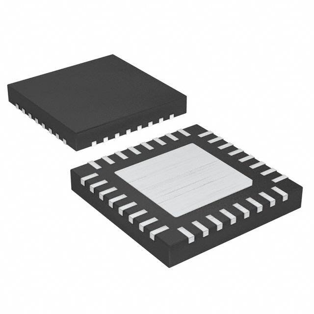
| 产品图片 |
|
| rohs | 符合RoHS无铅 / 符合限制有害物质指令(RoHS)规范要求 |
| 产品系列 | 电源管理 IC,开关控制器 ,ON Semiconductor NCP5380MNR2G- |
| 数据手册 | |
| 产品型号 | NCP5380MNR2G |
| 产品种类 | 开关控制器 |
| 供应商器件封装 | 32-QFN(5x5) |
| 其它名称 | NCP5380MNR2GOSDKR |
| 包装 | Digi-Reel® |
| 商标 | ON Semiconductor |
| 安装类型 | 表面贴装 |
| 安装风格 | SMD/SMT |
| 封装 | Reel |
| 封装/外壳 | 32-VFQFN 裸露焊盘 |
| 封装/箱体 | QFN-32 |
| 工作温度 | 0°C ~ 85°C |
| 工厂包装数量 | 5000 |
| 应用 | 控制器,Intel VR11 |
| 开关频率 | 390 kHz |
| 最大工作温度 | + 85 C |
| 最小工作温度 | 0 C |
| 标准包装 | 1 |
| 电压-输入 | 5V |
| 电压-输出 | 0.5 V ~ 1.6 V |
| 系列 | NCP5380 |
| 输入电压 | 4.75 V to 5.25 V |
| 输出数 | 1 |
| 输出电压 | 0 V to 1.6 V |
| 输出电流 | - 5 uA |
| 输出端数量 | 1 Output |

%20Renders/32-VQFN%20Exposed%20Pad.jpg)


- 商务部:美国ITC正式对集成电路等产品启动337调查
- 曝三星4nm工艺存在良率问题 高通将骁龙8 Gen1或转产台积电
- 太阳诱电将投资9.5亿元在常州建新厂生产MLCC 预计2023年完工
- 英特尔发布欧洲新工厂建设计划 深化IDM 2.0 战略
- 台积电先进制程称霸业界 有大客户加持明年业绩稳了
- 达到5530亿美元!SIA预计今年全球半导体销售额将创下新高
- 英特尔拟将自动驾驶子公司Mobileye上市 估值或超500亿美元
- 三星加码芯片和SET,合并消费电子和移动部门,撤换高东真等 CEO
- 三星电子宣布重大人事变动 还合并消费电子和移动部门
- 海关总署:前11个月进口集成电路产品价值2.52万亿元 增长14.8%


PDF Datasheet 数据手册内容提取
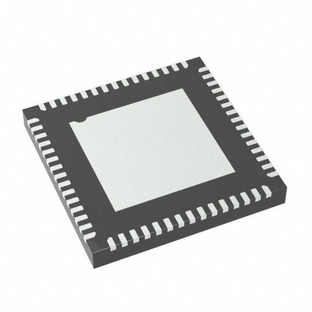
NCP5380, NCP5380A 7-Bit, Programmable, Single-Phase, Synchronous Buck Switching Regulator Controller http://onsemi.com General Description The NCP5380/A is a highly efficient, single−phase, synchronous MARKING buck switching regulator controller. With its integrated drivers, the DIAGRAM NCP5380/A is optimized for converting the silver box voltage to the supply voltage required by high performance Intel chipsets. An 1 internal 7−bit DAC is used to read a VID code directly from the 1 32 NCP5380 chipset. AWLYYWW(cid:2) QFN32, 5x5 (cid:2) The NCP5380/A uses a multimode architecture. It provides CASE 488AM programmable switching frequency that can be optimized for MN SUFFIX efficiency depending on the output current requirement. In addition, the NCP5380/A includes a programmable load line slope function to NCP5380 = Specific Device Code A = Assembly Location adjust the output voltage as a function of the load current so that the WL = Wafer Lot core voltage is always optimally positioned for a load transient. The YY = Year NCP5380/A also provides accurate and reliable current overload WW = Work Week protection and a delayed power−good output. The IC supports (cid:2) = Pb Free Package On−The−Fly (OTF) output voltage changes requested by the chipset. (Note: Microdot may be in either location) The NCP5380 is specified over the temperature range of 0°C to 85°C, while the NCP5380A extends the temperature range to −40°C to PIN CONFIGURATION 100°C. The NCP5380/A is available in a 32−lead QFN. 1234567 NDDDDDDD Features EVIVIVIVIVIVIVI • Single−chip Solution 1 • PWRGD VCC Fully Compatible with the Intel VR11 CPU Chipset Voltage IMON BST Regulator Specifications N/C NCP5380 DRVH • FBRTN SW Integrated MOSFET Drivers FB PVCC • ±8 mV Worst−case Differentially Sensed Core Voltage Error over COMP (Top View) DRVL GND PGND Temperature ILIM GND • Automatic Power−saving Modes Maximize Efficiency During Light FMTPEFBP Load Operation EPRMNEFM • Soft Transient Control Reduces Inrush Current and Audio Noise IRR RALLICSRCSSCO • C Independent Current Limit and Load Line Setting Inputs for Additional Design Flexibility ORDERING INFORMATION • Built−in Power−good Masking Supports Voltage Identification (VID) Device Package Shipping† OTF Transients • NCP5380MNR2G QFN−32 5000 / Tape & Reel 7−bit, Digitally Programmable DAC (Pb−Free) • Short−circuit Protection with Programmable Latchoff Delay NCP5380AMNR2G QFN−32 5000 / Tape & Reel • Current Monitor Output Signal (Pb−Free) • 32−lead QFN †For information on tape and reel specifications, • including part orientation and tape sizes, please This is a Pb−Free Device refer to our Tape and Reel Packaging Specifications Brochure, BRD8011/D. Applications • Desktop Power Supplies for Next−generation Intel Chipsets © Semiconductor Components Industries, LLC, 2011 1 Publication Order Number: April, 2011 − Rev. 3 NCP5380/D
NCP5380, NCP5380A V C V under the controller Controller GroundConnect Power Ground to SHORTPIN JP1 20.0kRA CBDNL470p CSenseRBCA 1.00k 0.01201nR22CA3C28 SSSense (cid:3) 1nC27R12 6041.00kRRAMVDC 200k80.6kRRPMRREF 10kRLIM ILIM22p8CFB7 6 5 40.1(cid:3)3866R192CMON1 RMON4.53k IMON PWRGD VR_ON VID0 VID1 VID2VID3 VID4 VID5 VID6 R kRP 390kRT 11109 IRRPEMF AGND COMPNFB FBRTN NC IMONPWRG VIEDN1333210 2 2 RT C D VID2 03 4DNL 111234 RLCLASIMRNEEPF P5380U1 VVVIIIDDD345222987 15 26 CSFB VID6 2 C 16 CSCOMPPGND DRVL PVCC SW DRVH BST VID725 1nC26 R551 .7n2.2n CCS1CS2 AGND33AGND17 18 19 20 21 RBST22 230VCC24 1(cid:3)C6 10R2 V 0 C 5 54.9k RCS1 1(cid:3)BST S 88.7k RCS2 Q 32 4 65 C84.7(cid:3) 3 7 4 5 1 8 23 6 Q 3 4 65 1 78 1 Q 2 4 7 4 5 1 8 3 6 2 Q 7 1 100k RPH DNL CSNB DNLRSNB8 560 n1 825V10(cid:3) C1 100 k(cid:2) % NTCRTH1 H/0.8 mL1 25V2101(cid:3)CC2 O 5V0(cid:3)3 h 2.5V220++C22 C41 m C33 V 25V10(cid:3)C4 VDC (cid:3) O U 2 ++ T .5V220(cid:3)C23 10 F(cid:3) 10 F(cid:3) x x 2 ++ 7 7 .52C V23 00 (cid:3) F C C 4 3 7 9 Figure 1. Application Schematic http://onsemi.com 2
NCP5380, NCP5380A GND VCC EN RPM RT RAMP BST UVLO Shutdown Oscillator and Bias DRVH COMP MOSFET SW VEA Driver FB − DRVL REF (cid:4) + + + PGND CSREF LLINE (cid:4) _ + OVP + − 1.55V OCP DAC + 200 mV Shutdown − Delay + CSREF Current Monitor IMON − Current + Limit DAC − 300 mV Circuit + CSREF PWRGD PWRGD Start Up − CSFB PWRGD Open Delay Drain Soft CSCOMP Transient ILIM Delay N/C Delay Disable GND Precision FBRTN Reference Soft Start and Soft VID Transient DAC Control DAC REF 7 6 5 4 3 2 1 F D D D D D D D E VI VI VI VI VI VI VI R I Figure 2. Functional Block Diagram ELECTRICAL CHARACTERISTICS VCC = 5.0 V, FBRTN = 112.5 mV, VVID = 1.25 V, TA = 0°C to 85°C (NCP5380), TA = −40°C to 100°C (NCP5380A), unless otherwise noted (Note 1). Current entering a pin (sunk by the device) has a positive sign. Parameter Symbol Conditions Min Typ Max Unit VOLTAGE CONTROL VOLTAGE ERROR AMPLIFIER (VEAMP) FB, LLINE Voltage Range (Note 2) VFB, Relative to CSREF = VDAC −200 +200 mV VLLINE FB, LLINE Offset Voltage (Note 2) VOSVEA Relative to CSREF = VDAC −0.5 +0.5 mV FB IFB −1.0 +1.0 (cid:3)A LLINE Bias Current ILLINE −10 +10 nA LLINE Positioning Accuracy VFB − Measured on FB relative to nominal VDAC mV VDAC −10°C to 100°C −78 −80 −82 −40°C to 100°C −77 −80 −83 COMP Voltage Range VCOMP Voltage range of interest 0.85 4.0 V 1. All limits at temperature extremes are guaranteed via correlation using standard statistical quality control (SQC). 2. Guaranteed by design or bench characterization, not production tested. http://onsemi.com 3
NCP5380, NCP5380A ELECTRICAL CHARACTERISTICS VCC = 5.0 V, FBRTN = 112.5 mV, VVID = 1.25 V, TA = 0°C to 85°C (NCP5380), TA = −40°C to 100°C (NCP5380A), unless otherwise noted (Note 1). Current entering a pin (sunk by the device) has a positive sign. Parameter Symbol Conditions Min Typ Max Unit VOLTAGE CONTROL VOLTAGE ERROR AMPLIFIER (VEAMP) COMP Current ICOMP COMP = 2.0 V, CSREF = VDAC FB forced 200 mV below CSREF −600 (cid:3)A FB forced 200 mV above CSREF 2.0 mA COMP Slew Rate SRCOMP CCOMP = 10 pF, CSREF = VDAC, Open V/(cid:3)s loop configuration FB forced 200 mV below CSREF 15 FB forced 200 mV above CSREF −20 Gain Bandwidth (Note 2) GBW Non−inverting unit gain 20 MHz configuration, RFB = 1 k(cid:2) VID DAC VOLTAGE REFERENCE VDAC Voltage Range (Note 2) See VID table 0 1.6 V VDAC Accuracy VFB − Measured on FB (includes offset), relative mV VDAC to nominal VDAC VDAC = 0.3 V to 1.2 V, −10°C to 100°C −7.0 +7.0 VDAC = 0.3 V to 1.2 V, −40°C to 100°C −9.0 +9.0 VDAC = 1.2125 V to 1.5 V, −40°C to 100°C −9.0 +9.0 VDAC Differential Nonlinearity −1 +1 LSB (Note 2) VDAC Line Regulation ΔVFB VCC = 4.75 V to 5.25 V 0.05 % VDAC Slew Rate Soft−start 0.0625 LSB/ Arbitrary VID step 1 (cid:3)s FBRTN Current IFBRTN 70 200 (cid:3)A BOOT VOLTAGE Boot Voltage Vboot 1.1 V Boot Voltage Timer tboot 50 70 100 (cid:3)s VID DAC INPUTS Input Low Voltage VIL VID(x) 0.5 0.3 V Input High Voltage VIH VID(x) 0.7 0.5 V Input Current IIN(VID) Sink current 1 (cid:3)A VID Transition Delay Time (Note 2) VID Code Change to FB Change 400 ns REFERENCE CURRENT IREF Voltage VIREF RIREF = 80 k(cid:2) to Set IREF = 20 (cid:3)A 1.55 1.6 1.65 (cid:3)A OSCILLATOR Frequency Range (Note 2) fOSC 0.3 3 MHz Oscillator Frequency FOSC TA = +25°C, VVID = 1.20 V, kHz Clocked PWM Mode RT = 60 k(cid:2) 900 1200 1500 RT = 120 k(cid:2) 465 600 725 RT = 180 k(cid:2) 300 400 500 RT Output Voltage VRT VVID = 1.6 V 1.08 1.2 1.35 V RPM Output Current IRPM VVID = 1.250 V, RT = 500 k(cid:2) −5 (cid:3)A RAMP Input Voltage VRAMP 0.9 1.0 1.1 V RAMP Input Current Range IRAMP EN = high 1 100 (cid:3)A RAMP Input Current in Shutdown EN = low or in UVLO, RAMP = 19V −0.5 +0.5 (cid:3)A 1. All limits at temperature extremes are guaranteed via correlation using standard statistical quality control (SQC). 2. Guaranteed by design or bench characterization, not production tested. http://onsemi.com 4
NCP5380, NCP5380A ELECTRICAL CHARACTERISTICS VCC = 5.0 V, FBRTN = 112.5 mV, VVID = 1.25 V, TA = 0°C to 85°C (NCP5380), TA = −40°C to 100°C (NCP5380A), unless otherwise noted (Note 1). Current entering a pin (sunk by the device) has a positive sign. Parameter Symbol Conditions Min Typ Max Unit CURRENT SENSE AMPLIFIER Offset Voltage VOS(CSA CSFB − CSREF −1.4 +1.4 mV ) Input Bias Current IBIAS(CS −50 +50 nA FB) Gain Bandwidth Product (Note 2) GBW(CS 20 MHz A) Slew Rate (Note 2) CCSCOMP = 10 pF 10 V/(cid:3)s Input Common−Mode Range (Note CSFB and CSREF 0 2 V 2) Output Voltage Range VCSCOM 0.05 2 V P Output Current ICSCOMP Source current −650 (cid:3)A Sink current 1 mA SWITCH AMPLIFIER Common−Mode Range (Note 2) VSW −400 +200 mV Input Resistance RSW 0.8 1.5 2.0 k(cid:2) Zero Current Switching Threshold VZCS(SW DCM Mode −6 mV ) DCM Minimum Off Time Masking tOFFMAS SW falling 700 ns K CURRENT LIMIT COMPARATOR ILIM Voltage VILIM− RILIMIT = 5 k(cid:2), −70 −100 −130 mV VCSCOM VCSREF − VCSCOMP = 100 mV P VILIM− RILIMIT = 5 k(cid:2), −1 0 1 mV VCSCOM VCSREF − VCSCOMP = 0 mV P Current Limit Latch Off Delay From OCP Event to PWRGD De−asser- 8 ms tion SOFT−START Soft−Start Time tss From FB = 0V to FB = Vboot 1.4 ms Soft−Start Delay From EN POS Edge to FB = 50 mV 200 (cid:3)s SOFT TRANSIENT CONTROL Output Voltage Positive Slew Rate 10 12.5 15 mV⁄(cid:3)s Output Voltage Negative Slew Rate −10 −12.5 −15 mV⁄(cid:3)s Extended PWRGD Masking VTH(ST) |ST − VVID|, ST falling 150 mV Comparator Threshold SYSTEM LOGIC INPUTS Input Voltage VEN Refers to driving signal level V Logic low, Isink = 1 (cid:3)A 0.3 Logic high, Isource = −5 (cid:3)A 0.7 V Input Current IEN VEN,VID[1:7] = 0 V 10 nA 0.2 V < VEN,VID[1:7] ≤ VCC 1 (cid:3)A 1. All limits at temperature extremes are guaranteed via correlation using standard statistical quality control (SQC). 2. Guaranteed by design or bench characterization, not production tested. http://onsemi.com 5
NCP5380, NCP5380A ELECTRICAL CHARACTERISTICS VCC = 5.0 V, FBRTN = 112.5 mV, VVID = 1.25 V, TA = 0°C to 85°C (NCP5380), TA = −40°C to 100°C (NCP5380A), unless otherwise noted (Note 1). Current entering a pin (sunk by the device) has a positive sign. Parameter Symbol Conditions Min Typ Max Unit POWER GOOD CSREF Undervoltage Threshold VUV(CSR For VID = 1.2 V −360 −300 −240 mV EF) CSREF Overvoltage Threshold VOV(CSR 150 200 250 mV EF) CSREF Crowbar (Overvoltage VCB(CSR FBRTN = 112.5 mV 1.5 1.55 1.6 V Protection) Threshold EF) CSREF Reverse Voltage Detection VRVP(CS CSREF falling −350 −300 mV Threshold REF) CSREF rising −75 −5 mV PWRGD Output Low Voltage VOL(PWR ISINK(PWRGD) = 4 mA 75 100 mV GD) PWRGD Output Leakage Current VPWRDG = 3.3 V 0.5 (cid:3)A PWRGD Masking Time 100 (cid:3)s PWRGD delay Time tPWRGD 6 10 11 ms CURRENT MONITOR IMON Output Current IIMON VCSREF − VCSCOMP = 100 mV 9 10 11 (cid:3)A IMON Output Current IIMON VCSREF − VCSCOMP = 10 mV 0.9 1 1.1 (cid:3)A IMON Clamp VIMON 1.0 1.15 V HIGH−SIDE MOSFET DRIVER Output Resistance, Sourcing Cur- BST − SW = 4.6 V 1.6 3.3 (cid:2) rent Output Resistance, Sinking Current BST − SW = 4.6 V 1.3 2.8 (cid:2) Transition Times trDRVH, BST − SW = 4.6 V, CL = 3 nF 15 35 ns tfDRVH BST − SW = 4.6 V, CL = 3 nF 13 31 ns Dead Delay Times tpdhDRV BST − SW = 4.6 V 20 45 ns H BST Quiescent Current EN = low, shutdown 5 15 (cid:3)A EN = high, no switching 200 (cid:3)A LOW−SIDE MOSFET DRIVER Output Resistance, Sourcing Cur- 1.4 3.0 (cid:2) rent Output Resistance, Sinking Current 1 2.7 (cid:2) Transition Times trDRVL CL = 3 nF 15 35 ns tfDRVL CL = 3 nF 14 35 ns Propagation Delay Times tpdhDRV CL = 3 nF 24 40 ns L SW Transition Timeout tTO(SW) BST − SW = 4.6 V 150 250 450 ns Zero−Crossing Threshold VZC 1.5 V PVCC Quiescent Current EN = low, shutdown 14 50 (cid:3)A EN = high, no switching 450 (cid:3)A BOOTSTRAP RECTIFIER Output Resistance 4.0 8.0 11 (cid:2) SOFT STOP CSREF Resistance to GND EN = low or latch off 70 (cid:2) 1. All limits at temperature extremes are guaranteed via correlation using standard statistical quality control (SQC). 2. Guaranteed by design or bench characterization, not production tested. http://onsemi.com 6
NCP5380, NCP5380A ELECTRICAL CHARACTERISTICS VCC = 5.0 V, FBRTN = 112.5 mV, VVID = 1.25 V, TA = 0°C to 85°C (NCP5380), TA = −40°C to 100°C (NCP5380A), unless otherwise noted (Note 1). Current entering a pin (sunk by the device) has a positive sign. Parameter Symbol Conditions Min Typ Max Unit SUPPLY Supply Voltage Range (Note 2) VCC 4.5 5.5 V Supply Current Normal mode 4.2 10 mA EN = 0 V 60 200 (cid:3)A VCC OK Threshold Voltage VCCOK VCC rising 4.4 4.5 V VCC UVLO Threshold Voltage VCCUVL VCC falling 4.0 4.2 V O UVLO Hysteresis (Note 2) 250 mV 1. All limits at temperature extremes are guaranteed via correlation using standard statistical quality control (SQC). 2. Guaranteed by design or bench characterization, not production tested. http://onsemi.com 7
NCP5380, NCP5380A Timing Diagram Timing is referenced to the 90% and 10% points, unless otherwise noted. IN tpdlDRVL tfDRVL trDRVL DRVL tpdlDRVH tpdhDRVH trDRVH tfDRVH VTH VTH DRVH (WITH RESPECT TO SW) tpdhDRVL SW Figure 3. Timing Diagram ABSOLUTE MAXIMUM RATING Parameter Rating VCC −0.3 V to +6.0 V FBRTN, PGND −0.3 V to +0.3 V BST DC −0.3 V to +28 V t < 200 ns −0.3 V to +33 V BST to SW −0.3 V to +6.0 V DRVH, SW DC −5.0 V to +21 V t < 200 ns −10 V to +26 V DRVH to SW −0.3 V to +6.0 V DRVL to PGND DC −0.3 V to +6.0 V t < 200 ns −5.0 V to +6.0 V RAMP (in Shutdown) DC −0.3 V to +21 V t < 200 ns −0.3 V to +26 V All Other Inputs and Outputs −0.3 V to +6.0 V Storage Temperature −65°C to +150°C Operating Ambient Temperature Range −40°C to 100°C Operating Junction Temperature 125°C Thermal Impedance (θJA) 2−Layer Board 32.6°C/W Lead Temperature Soldering (10 sec) 300°C Infrared (15 sec) 260°C Stresses exceeding Maximum Ratings may damage the device. Maximum Ratings are stress ratings only. Functional operation above the Recommended Operating Conditions is not implied. Extended exposure to stresses above the Recommended Operating Conditions may affect device reliability. http://onsemi.com 8
NCP5380, NCP5380A Pin Function Descriptions Pin No. Mnemonic Description 1 PWRGD Power−Good Output. Open−drain output. A low logic state means that the output voltage is outside of the VID DAC defined range. 2 IMON Current Monitor Output. This pin sources current proportional to the output load current. A resistor connected to VSS Sense sets the current monitor gain. 3 N/C 4 FBRTN Feedback Return Input/Output. This pin remotely senses the output voltage. It is also used as the ground return for the VID DAC and the voltage error amplifier blocks. It is also used to adjust the no−load offset. 5 FB Voltage Error Amplifier Feedback Input. The inverting input of the voltage error amplifier. 6 COMP Voltage Error Amplifier Output and Frequency Compensation Point. 7 GND Analog and digital signal ground. 8 ILIM Current Limit Set pin. Connect a resistor between ILIM and CSCOMP to the current limit threshold. 9 IREF This pin sets the internal bias currents. A 100 k(cid:2) is connected from IREF to ground. 10 RPM RPM Mode Timing Control Input. A resistor is connected from RPM to ground sets the RPM mode turn−on threshold voltage. 11 RT PWM Oscillator Frequency Setting Input. An external resistor from this pin to GND sets the PWM oscillator frequency. 12 RAMP PWM Ramp Slope Setting Input. An external resistor from the converter input voltage node to this pin sets the slope of the internal PWM stabilizing ramp. 13 LLINE Load Line Programming Input. The center point of a resistor divider connected between CSREF and CSCOMP tied to this pin sets the load line slope. 14 CSREF Current Sense Reference Input. This pin must be connected to the opposite side of the output inductor. 15 CSFB Noninverting Input of the Current Sense Amplifier. The combination of a resistor from the switch node to this pin and the feedback network from this pin to the CSCOMP pin sets the gain of the current sense amplifier. 16 CSCOMP Current Sense Amplifier Output. 17 GND Analog and Digital Signal Ground. 18 PGND Low−Side Driver Power Ground. This pin should be connected close to the source of the lower MOSFET(s). 19 DRVL Low−Side Gate Drive Output. 20 PVCC Power Supply Input/Output of Low−Side Gate Driver. 21 SW Current Return For High−Side Gate Drive. 22 DRVH High−Side Gate Drive Output. 23 BST High−Side Bootstrap Supply. A capacitor from this pin to SW holds the bootstrapped voltage while the high−side MOSFET is on. 24 VCC Power Supply Input/Output of the Controller. 25 to VID7 to VID1 Voltage Identification DAC Inputs. A 7−bit word (the VID code) programs the DAC output voltage, the 31 reference voltage of the voltage error amplifier without a load (see the VID code table, Table 4). In normal operation mode, the VID DAC output programs the output voltage to a value within the 0 V to 1.6 V range (with FBRTN = 112.5 mV). The input is actively pulled down. 32 EN Enable Input. Driving this pin low shuts down the chip, disables the driver outputs, and pulls PWRGD low. Flag PGND High current power supply return via metal pad (flag) underneath package. Connect to pin 7. http://onsemi.com 9
NCP5380, NCP5380A Typical Performance Characteristics V = 1.5 V, T = 20°C to 100°C, unless otherwise noted. VID A Output Voltage Output Voltage Switch Node Switch Node Inductor Current Inductor Current Low Side Gate Drive Low Side Gate Drive Figure 4. DCM Waveforms, 1 A Load Current Figure 5. CCM Waveforms, 10 A Load Current Output Voltage Output Voltage Switch Node Switch Node Load Current Load Current Figure 6. Load Transient, 2 A to 10 A, V = 19 V Figure 7. Load Transient, 2 A to 10 A, V = 19 V IN IN OUTPUT VOLTAGE Output Voltage VID 0 Figure 8. VID on the Fly, 1.25 V to 0.825 V Figure 9. Output Ripple, 15 A Load, C = 470 (cid:2)F, X C = 44 (cid:2)F Z http://onsemi.com 10
NCP5380, NCP5380A Theory of Operation The NCP5380/A is a ramp−pulse−modulated (RPM) Operation Modes controller for synchronous buck power supply. The internal The NCP5380/A runs in RPM mode for the purpose of fast 7−bit VID DAC conforms to the Intel VR11 specifications. transient response and high light load efficiency. During the The NCP5380/A is a stable, high performance architecture following transients, the NCP5380/A runs in PWM mode: • that includes Soft−Start • High speed response at the lowest possible switching • Soft transient: the period of 100 (cid:3)s following any VID frequency and minimal count of output decoupling change capacitors • Current overload • Minimized thermal switching losses due to lower frequency operation • High accuracy load line regulation • High power conversion efficiency with a light load by automatically switching to DCM operation VRMP IR = AR X IRAMP Flip−Flop 5.0 V - S Q + VCC Gate - + RD Driver BST CR BST DRVH IN DRVH RI L SW 400 ns Flip−Flop DCM SW DRVL 1.0 V DRVL Q S Q Q LOAD RD R2 R1 - - + + + 30 mV R2 R1 − 1.0 V CSREF + − + VDC − + + (cid:4) (cid:4) - - +VCS + CSFB COMP FB FBRTN LLINE CSCOMP RCS RPH RA CA CB CCS CFB RFB Figure 10. RPM Mode Operation http://onsemi.com 11
NCP5380, NCP5380A 5.0 V VCC Gate Driver IR = AR X IRAMP BST BST Flip−Flop DRVH Clock DRVH RI L Oscillator S Q IN SW SW DRVL + DRVL RD CR - LOAD VCC - CSREF AD + 0.2 V + − + VDC − + Ramp + (cid:4) (cid:4) - - +VCS + CSFB COMP FB FBRTN LLINE CSCOMP RCS RPH RA CA CB CCS CFB RFB Figure 11. PWM Mode Operation Setting Switch Frequency Master Clock Frequency in PWM Mode mode, the combination of the VID DAC and error amplifier When the NCP5380/A runs in PWM, the clock frequency maintain the output voltage for a worst−case scenario within is set by an external resistor connected from the RT pin to ±8mV of the full operating output voltage and temperature GND. The frequency varies with the VID voltage: the lower range. the VID voltage, the lower the clock frequency. The The output voltage is sensed between the FB and FBRTN variation of clock frequency with VID voltage maintains pins. FB should be connected through a resistor to the constant output ripple and improves power conversion positive regulation point. FBRTN should be connected efficiency at lower VID voltages. directly to the negative remote sensing point. The internal VID DAC and precision voltage reference are referenced to Switching Frequency in RPM Mode FBRTN thus allowing no load offset to be set using this pin. When the NCP5380/A operates in RPM mode, its switching frequency is controlled by the ripple voltage on Output Current Sensing the COMP pin. Each time the COMP pin voltage exceeds the The NCP5380/A includes a dedicated current sense RPM pin voltage threshold level determined by the VID amplifier (CSA) to monitor the total output current of the voltage and the external resistor connected between RPM converter for proper voltage positioning vs. load current and and ground, an internal ramp signal is started and DRVH is for overcurrent detection. Sensing the current delivered to driven high. The slew rate of the internal ramp is the load is an inherently more accurate method than programmed by the current entering the RAMP pin. detecting peak current or sampling the current across a sense One−third of the RAMP current charges an internal ramp element, such as the low−side MOSFET. The current sense capacitor (5 pF typical) and creates a ramp. When the amplifier can be configured several ways, depending on internal ramp signal intercepts the COMP voltage, the system optimization objectives, and the current information DRVH pin is reset low. can be obtained by In continuous current mode, the switching frequency of • Output inductor ESR sensing without the use of a RPM operation is almost constant. While in discontinuous thermistor for the lowest cost current conduction mode, the switching frequency is • Output inductor ESR sensing with the use of a reduced as a function of the load current. thermistor that tracks inductor temperature to improve accuracy Differential Sensing of Output Voltage • The NCP5380/A combines differential sensing with a Discrete resistor sensing for the highest accuracy high accuracy VID DAC, referenced by a precision band gap At the positive input of the CSA, the CSREF pin is source and a low offset error amplifier, In steady−state connected to the output voltage. At the negative input (that http://onsemi.com 12
NCP5380, NCP5380A is, the CSFB pin of the CSA), signals from the sensing output that can be pulled up through an external resistor to element (in the case of inductor DCR sensing, signals from a voltage rail − not necessarily the same VCC voltage rail the switch node side of the output inductors) are connected that is running the controller. A logic high level indicates with a resistor. The feedback resistor between the CSCOMP that the output voltage is within the voltage limits defined by and CSFB pins sets the gain of the current sense amplifier, a range around the VID voltage setting. PWRGD goes low and a filter capacitor is placed in parallel with this resistor. when the output voltage is outside of this range. The current information is then given as the voltage Following the CPU specification, the PWRGD range is difference between the CSCOMP and CSREF pins. This defined to be 300 mV less than and 200 mV greater than the signal is used internally as a differential input for the current actual VID DAC output voltage. To prevent a false alarm, limit comparator. the power−good circuit is masked during any VID change An additional resistor divider connected between the and during soft−start. The duration of the PWRGD mask is CSCOMP and CSREF pins with the midpoint connected to set to approximately 100 (cid:3)s by an internal timer. In addition, the LLINE pin can be used to set the load line. The current for a VID change from high to low, there is an additional information to set the load line is then given as the voltage period of PWRGD masking before the internal DAC voltage difference between the LLINE and CSREF pins. This drops within 200 mV of the new lower VID DAC output configuration allows the load line slope to be set voltage, as shown in Figure 12. independent from the current limit threshold. If the current limit threshold and load line do not have to be set VID SIGNAL CHANGE independently, the resistor divider between the CSCOMP and CSREF pins can be omitted and the CSCOMP pin can Internal DAC be connected directly to LLINE. To disable voltage VOLTAGE positioning entirely (that is, to set no load line), LLINE 200mV should be tied to CSREF. To provide the best accuracy for current sensing, the CSA PWRGD 100 (cid:3)s 100 (cid:3)s MASK 100μs 100μs has a low offset input voltage and the sensing gain is set by an external resistor ratio. Figure 12. PWRGD Masking for VID Change Active Impedance Control Mode Power−Up Sequence and Soft−Start To control the dynamic output voltage droop as a function The power−on ramp−up time of the output voltage is set of the output current, the signal that is proportional to the internally. The power−up sequence is illustrated in total output current, converted from the voltage difference Figure13. between LLINE and CSREF, can be scaled to be equal to the required droop voltage. This droop voltage is calculated by VCC = 5.0 V multiplying the droop impedance of the regulator by the output current. This value is used as the control voltage of EN the PWM regulator. The droop voltage is subtracted from the VBOOT = 1.0 V DAC reference output voltage, and the resulting voltage is DAC AND VCORE used as the voltage positioning setpoint. The arrangement results in an enhanced feedforward response. tBOOT Voltage Control Mode Figure 13. Power−Up Sequence for CPU A high−gain bandwidth error amplifier is used for the voltage mode control loop. The noninverting input voltage VID Change and Soft Transient is set via the 7−bit VID DAC. The noninverting input When a VID input changes, the NCP5380/A detects the voltage is offset by the droop voltage as a function of current, change but ignores new code for a minimum of 400 ns. This commonly known as active voltage positioning. The output delay is required to prevent the device from reacting to digital of the error amplifier is the COMP pin, which sets the signal skew while the 7−bit VID input code is in transition. termination voltage of the internal PWM ramps. Additionally, the VID change triggers a PWRGD masking At the negative input, the FB pin is tied to the output sense timer to prevent a PWRGD failure. Each VID change resets location using R , a resistor for sensing and controlling the and retriggers the internal PWRGD masking timer. B output voltage at the remote sensing point. The main loop The NCP5380/A provides a soft transient function to compensation is incorporated in the feedback network reduce inrush current during VID transitions. Reducing the connected between the FB and COMP pins. inrush current helps decrease the acoustic noise generated by the MLCC input capacitors and inductors. Power−Good Monitoring The soft transient feature is implemented internally. When The power−good comparator monitors the output voltage a new VID code is detected, the NCP5380/A steps via the CSREF pin. The PWRGD pin is an open−drain http://onsemi.com 13
NCP5380, NCP5380A sequentially through each VID voltage to the final VID Light Load RPM DCM Operation voltage. The NCP5380/A operates in RPM mode. With higher loads, the NCP5380/A operates in continuous conduction Current Limit, Short−Circuit, and Latchoff Protection mode (CCM), and the upper and lower MOSFETs run The NCP5380/A has an adjustable current limit set by the synchronously and in complementary phase. See Figure15 RCLIM resistor. The NCP5380/A compares a programmable for the typical waveforms of the NCP5380/A running in current−limit set point to the voltage from the output of the CCM with a 7 A load current. current−sense amplifier. The level of current limit is set with the resistor from the ILIM pin to CSCOMP. During OUTPUT VOLTAGE 20mV/DIV 4 operation, the voltage on ILIM is equal to the voltage on CSREF. The current through the external resistor connected between ILIM and CSCOMP is then compared to the INDUCTOR CURRENT 5A/DIV internal current limit current Icl. If the current generated through this resistor into the ILIM pin(Ilim) exceeds the 2 internal current−limit threshold current (Icl), the internal SWITCH NODE 5V/DIV current−limit amplifier controls the internal COMP voltage to maintain the average output current at the limit. 3 Normally, the NCP5380/A operates in RPM mode. LOW−SIDE GATE DRIVE 5V/DIV During a current overload, the NCP5380/A switches to 1 PWM mode. With low impedance loads, the NCP5380/A operates in a 1ms/DIV constant current mode to ensure that the external MOSFETs Figure 15. Single−Phase Waveforms in CCM and inductor function properly and to protect the CPU. With With lighter loads, the NCP5380/A enters discontinuous a low constant impedance load, the output voltage decreases conduction mode (DCM). Figure 16 shows a typical to supply only the set current limit. If the output voltage single-phase buck with one upper FET, one lower FET, an drops below the power−good limit, the PWRGD signal output inductor, an output capacitor, and a load resistor. transitions. After the PWRGD single transitions, internal Figure 17 shows the path of the inductor current with the waits 7 ms before latching off the NCP5380/A. upper FET on and the lower FET off. In Figure 18 the Figure 14 shows how the NCP5380/A reacts to a current high-side FET is off and the low-side FET is on. In CCM, if overload. one FET is on, its complementary FET must be off; however, in DCM, both high- and low-side FETs are off and no current flows into the inductor (see Figure 19). Figure 20 shows the inductor current and switch node voltage in DCM. In DCM with a light load, the NCP5380/A monitors the switch node voltage to determine when to turn off the low-side FET. Figure 20 shows a typical waveform in DCM with a 1 A load current. Between t1 and t2, the inductor current ramps down. The current flows through the source drain of the low-side FET and creates a voltage drop across the FET with a slightly negative switch node. As the inductor current ramps down to 0 A, the switch voltage approaches 0 V, as seen just before t2. When the switch voltage is approximately −6 mV, the low-side FET is turned off. Figure 20 shows a small, dampened ringing at t2. This is Figure 14. Current Overload caused by the LC created from capacitance on the switch node, including the CDS of the FETs and the output inductor. The latchoff function can be reset either by removing and This ringing is normal. reapplying VCC or by briefly pulling the EN pin low. The NCP5380/A automatically goes into DCM with a During startup, when the output voltage is below 200mV, light load. Figure 21 shows the typical DCM waveform of a secondary current limit is active. This is necessary because the NCP5380/A with a 1 A load current. As the load the voltage swing of CSCOMP cannot extend below ground. increases, the NCP5380/A enters into CCM. In DCM, This secondary current limit clamp controls the minimum frequency decreases with load current, and switching internal COMP voltage to the PWM comparators to 1.5V. frequency is a function of the inductor, load current, input This limits the voltage drop across the low−side MOSFETs voltage, and output voltage. through the current balance circuitry. http://onsemi.com 14
NCP5380, NCP5380A Q1 DRVH SWITCH OUTPUT NODE L VOLTAGE Inductor + INPUT Q2 Current − VOLTAGE LOAD C DRVL Figure 16. Buck Topology Switch Node ON Voltage L + − LOAD OFF C t t t t t 0 1 2 3 4 Figure 20. Inductor Current and Switch Node in DCM Figure 17. Buck Topology Inductor Current During t0 and t1 OUTPUT VOLTAGE 4 20mV/DIV OFF SWITCH NODE L 5V/DIV + 2 − LOAD ON C INDUCTOR CURRENT 3 5A/DIV 1 Figure 18. Buck Topology Inductor Current During LOW−SIDE GATE DRIVE 5V/DIV t and t 1 2 2(cid:3)s/DIV Figure 21. Single−Phase Waveforms in DCM with 1 A Load Current OFF L Output Crowbar + To protect the load and output components of the supply, − the DRVL output is driven high (turning the low−side LOAD OFF C MOSFETs on) and DRVH is driven low (turning the high−side MOSFETs off) when the output voltage exceeds the CPU OVP threshold. Figure 19. Buck Topology Inductor Current During Turning on the low−side MOSFETs forces the output t2 and t3 capacitor to discharge and the current to reverse due to current build up in the inductors. If the output overvoltage is due to a drain−source short of the high−side MOSFET, turning on the low−side MOSFET results in a crowbar across the input voltage rail. The crowbar action blows the fuse of the input rail, breaking the circuit and thus protecting the CPU chipset from destruction. When the OVP feature is triggered, the NCP5380 is latched off. The latchoff function can be reset by removing and reapplying VCC to the NCP5380/A or by briefly pulling the EN pin low. http://onsemi.com 15
NCP5380, NCP5380A Reverse Voltage Protection voltage is less than the V threshold or the EN pin is CCUVLO Very large reverse current in inductors can cause negative logic low, the NCP5380/A shuts off. In shutdown mode, the output voltage, which is harmful to the chipset and other controller holds DRVH and DRVL low, shorts the capacitors output components. The NCP5380/A provides a reverse of the SS and PGDELAY pins to ground, and drives voltage protection (RVP) function without additional PWRGD to low. system cost. The output voltage is monitored through the The user must adhere to proper power−supply sequencing CSREF pin. When the CSREF pin voltage drops to less than during startup and shutdown of the NCP5380/A. All input −190mV, the NCP5380/A triggers the RVP function by pins must be at ground prior to removing or applying V , CC setting both DRVH and DRVL low, thus turning off all and all output pins should be left in high impedance state MOSFETs. The reverse inductor currents can be quickly while V is off. CC reset to 0 by discharging the built−up energy in the inductor into the input dc voltage source via the forward−biased body Output Current Monitor diode of the high−side MOSFETs. The RVP function is The NCP5380/A includes an output current monitor terminated when the CSREF pin voltage returns to greater function. The IMON pin outputs an accurate current that is directly proportional to the output current. This current is than −150 mV. then run through a parallel RC connected from the IMON Sometimes the crowbar feature inadvertently results in pin to the FBRTN pin to generate an accurately scaled and negative voltage because turning on the low−side MOSFETs filtered voltage. The maximum voltage on IMON is results in a very large reverse inductor current. To prevent internally clamoed by the NCP5380/A at 1.15 V. damage to the chipset caused from negative voltage, the NCP5380/A maintains its RVP monitoring function even Output Voltage No-load Offset Adjustment after OVP latchoff. During OVP latchoff, if the CSREF pin The NCP5380/A output voltage can be offset from the voltage drops to less than −190 mV, the low−side MOSFETs nominal VID settings by adjusting one resistor value. The is turned off by setting DRVL low. DRVL will be set high following figure shows the components used for setting the again when the CSREF voltage recovers to greater than no-load output offset voltage. +50mV. Figure 22 shows the reverse voltage protection function of VCC (pin 24) the NCP5380/A. The CSREF pin is disconnected from the output voltage and pulled negative. As the CSREF pin drops Rofs to less than −190 mV, the low−side and high−side FETs turn off. FBRTN (pin 4) 0.1 (cid:3)F 20 −Vout Return 3 CSREF Figure 23. Setting the Output Offset Voltage The nominal VID table for the NCP5380/A is based on the PWRGD 2 voltage at FBRTN being 112.5 mV (Rofs nominal of DRVH 866ohms). If it is desired to adjust the no-load output 4 voltage to be above or below VID, then the value of R can ofs be changed. If we define the no-load offset from VID as DRVL V , then the following can be used to determine the value nlofs 1 for R (given V = 5 V); ofs CC (cid:3) (cid:6) Figure 22. NCP5380 RVP Function R (cid:2) 5 (cid:5)1 (cid:7)20 ofs 0.1125(cid:4)V Output Enable and UVLO nlofs For the NCP5380/A to begin switching, the VCC supply NOTE: The 20 ohm resistor and 0.1 (cid:3)F capacitor nominal voltage to the controller must be greater than the V CCOK values are fixed based on the design of the NCP5380/A so threshold and the EN pin must be driven high. If the V CC only R should be adjusted for changing the no−load offset. ofs http://onsemi.com 16
NCP5380, NCP5380A VID Codes (FBRTN = 112.5 mV) VID7 VID6 VID5 VID4 VID3 VID2 VID1 Output 0 0 0 0 0 0 1 1.6000 0 0 0 0 0 1 0 1.5875 0 0 0 0 0 1 1 1.5750 0 0 0 0 1 0 0 1.5625 0 0 0 0 1 0 1 1.5500 0 0 0 0 1 1 0 1.5375 0 0 0 0 1 1 1 1.5250 0 0 0 1 0 0 0 1.5125 0 0 0 1 0 0 1 1.5000 0 0 0 1 0 1 0 1.4875 0 0 0 1 0 1 1 1.4750 0 0 0 1 1 0 0 1.4625 0 0 0 1 1 0 1 1.4500 0 0 0 1 1 1 0 1.4375 0 0 0 1 1 1 1 1.4250 0 0 1 0 0 0 0 1.4125 0 0 1 0 0 0 1 1.4000 0 0 1 0 0 1 0 1.3875 0 0 1 0 0 1 1 1.3750 0 0 1 0 1 0 0 1.3625 0 0 1 0 1 0 1 1.3500 0 0 1 0 1 1 0 1.3375 0 0 1 0 1 1 1 1.3250 0 0 1 1 0 0 0 1.3125 0 0 1 1 0 0 1 1.3000 0 0 1 1 0 1 0 1.2875 0 0 1 1 0 1 1 1.2750 0 0 1 1 1 0 0 1.2625 0 0 1 1 1 0 1 1.2500 0 0 1 1 1 1 0 1.2375 0 0 1 1 1 1 1 1.2250 0 1 0 0 0 0 0 1.2125 0 1 0 0 0 0 1 1.2000 0 1 0 0 0 1 0 1.1875 0 1 0 0 0 1 1 1.1750 0 1 0 0 1 0 0 1.1625 0 1 0 0 1 0 1 1.1500 0 1 0 0 1 1 0 1.1375 0 1 0 0 1 1 1 1.1250 0 1 0 1 0 0 0 1.1125 0 1 0 1 0 0 1 1.1000 0 1 0 1 0 1 0 1.0875 0 1 0 1 0 1 1 1.0750 0 1 0 1 1 0 0 1.0625 0 1 0 1 1 0 1 1.0500 http://onsemi.com 17
NCP5380, NCP5380A VID Codes (FBRTN = 112.5 mV) VID7 VID6 VID5 VID4 VID3 VID2 VID1 Output 0 1 0 1 1 1 0 1.0375 0 1 0 1 1 1 1 1.0250 0 1 1 0 0 0 0 1.0125 0 1 1 0 0 0 1 1.0000 0 1 1 0 0 1 0 0.9875 0 1 1 0 0 1 1 0.9750 0 1 1 0 1 0 0 0.9625 0 1 1 0 1 0 1 0.9500 0 1 1 0 1 1 0 0.9375 0 1 1 0 1 1 1 0.9250 0 1 1 1 0 0 0 0.9125 0 1 1 1 0 0 1 0.9000 0 1 1 1 0 1 0 0.8875 0 1 1 1 0 1 1 0.8750 0 1 1 1 1 0 0 0.8625 0 1 1 1 1 0 1 0.8500 0 1 1 1 1 1 0 0.8375 0 1 1 1 1 1 1 0.8250 1 0 0 0 0 0 0 0.8125 1 0 0 0 0 0 1 0.8000 1 0 0 0 0 1 0 0.7875 1 0 0 0 0 1 1 0.7750 1 0 0 0 1 0 0 0.7625 1 0 0 0 1 0 1 0.7500 1 0 0 0 1 1 0 0.7375 1 0 0 0 1 1 1 0.7250 1 0 0 1 0 0 0 0.7125 1 0 0 1 0 0 1 0.7000 1 0 0 1 0 1 0 0.6875 1 0 0 1 0 1 1 0.6750 1 0 0 1 1 0 0 0.6625 1 0 0 1 1 0 1 0.6500 1 0 0 1 1 1 0 0.6375 1 0 0 1 1 1 1 0.6250 1 0 1 0 0 0 0 0.6125 1 0 1 0 0 0 1 0.6000 1 0 1 0 0 1 0 0.5875 1 0 1 0 0 1 1 0.5750 1 0 1 0 1 0 0 0.5625 1 0 1 0 1 0 1 0.5500 1 0 1 0 1 1 0 0.5375 1 0 1 0 1 1 1 0.5250 1 0 1 1 0 0 0 0.5125 1 0 1 1 0 0 1 0.5000 1 1 1 1 1 1 1 OFF http://onsemi.com 18
NCP5380, NCP5380A APPLICATION INFORMATION The design parameters for a typical VR11−compliant CPU A (cid:7)L core VR application are as follows: RR(cid:2)3(cid:7)A (cid:7)R R (cid:7)C (eq. 2) • D DS R Maximum Input Voltage (V ) = 19 V INMAX • 0.5(cid:7)360nH Minimum Input Voltage (VINMIN) = 8.0 V R (cid:2) • Output Voltage by VID Setting (V ) = 1.2375 V R 3(cid:7)5(cid:7)5.2m(cid:2)(cid:7)5pF VID • Maximum Output Current (IO) = 14 A Where: • Droop Resistance (RO) = 6.9 m(cid:2) AR is the internal ramp amplifier gain. • A is the current balancing amplifier gain. Nominal Output Voltage at 15 A Load D R is the total low−side MOSFET ON−resistance, (V ) = 1.1409 V DS OFL • Static output voltage drop from no load to full load CR is the internal ramp capacitor value. Another consideration in the selection of RR is the size of ((cid:5)V) = V − V = 1.2375 V − 1.1409 V = ONL OFL the internal ramp voltage (see Equation 3). For stability and 96.6 mV noise immunity, keep this ramp size larger than 0.5 V. Taking • Maximum Output Current Step ((cid:5)IO) = 11 A this into consideration, the value of RR is selected as 280 k(cid:2). • Number of Phases (n) = 1 The internal ramp voltage magnitude can be calculated • Switching Frequency (fSW) = 390 kHz using: • Duty Cycle at Maximum Input Voltage (D ) = MAX A (cid:7)(1(cid:5)D)(cid:7)V 0.15 V V (cid:2) R VID (eq. 3) • R R (cid:7)C (cid:7)f Duty Cycle at Minimum Input Voltage (DMIN) = 0.065 R R sw 0.5(cid:7)(1(cid:5)0.065)(cid:7)1.2375V SETTING THE CLOCK FREQUENCY FOR PWM V (cid:2) (cid:2)0.89V The NCP5380/A operates in fixed frequency PWM mode R 462k(cid:2)(cid:7)5pF(cid:7)280kHz during startup, for 100 (cid:3)s after a VID change, and in current The size of the internal ramp can be made larger or limit. In PWM operation, the NCP5380/A uses a smaller. If it is made larger, then stability and transient fixed−frequency control architecture. The frequency is set response improves, but thermal balance degrades. Likewise, by an external timing resistor (RT). The clock frequency if the ramp is made smaller, then thermal balance improves determines the switching frequency, which relates directly at the sacrifice of transient response and stability. The factor to the switching losses and the sizes of the inductors and of three in the denominator of Equation 2 sets a minimum input and output capacitors. For example, a clock frequency ramp size that gives an optimal balance for good stability, of 300 kHz sets the switching frequency to 300 kHz. This transient response, and thermal balance. selection represents the trade−off between the switching COMP PIN RAMP losses and the minimum sizes of the output filter In addition to the internal ramp, there is a ramp signal on components. To achieve a 300 kHz oscillator frequency at a VID voltage of 1.2 V, RT must be 391 k(cid:2). Alternatively, the the COMP pin due to the droop voltage and output voltage ramps. This ramp amplitude adds to the internal ramp to value for RT can be calculated by using the following produce the following overall ramp signal at the PWM equation: input: V (cid:4)1.0V R (cid:2) VID (cid:5)16k(cid:2) (eq. 1) V T 2(cid:7)f (cid:7)9pF V (cid:2) R (eq. 4) sw RT 1(cid:5) 2(cid:7)(1(cid:5)D) Where: f(cid:7)Cx(cid:7)RO 9 pF and 16 k(cid:2) are internal IC component values. Where C is the total bulk capacitance, and R is the droop X O V is the VID voltage in volts. VID resistance of the regulator. f is the switching frequency in hertz. SW For this example, the overall ramp signal is 0.23 V. For good initial accuracy and frequency stability, it is recommended to use a 1% resistor. SETTING THE SWITCHING FREQUENCY FOR RPM OPERATION RAMP RESISTOR SELECTION During the RPM operation, the NCP5380/A runs in The ramp resistor (R ) is used for setting the size of the R pseudoconstant frequency if the load current is high enough internal PWM ramp. The value of this resistor is chosen to for continuous current mode. While in DCM, the switching provide the best combination of thermal balance, stability, frequency is reduced with the load current in a linear and transient response. Use this equation to determine a manner. To save power with light loads, lower switching starting value: http://onsemi.com 19
NCP5380, NCP5380A frequency is usually preferred during RPM operation. If the resultant ripple voltage is less than the initially However, the V ripple specification of VR11 sets a selected value, the inductor can be changed to a smaller CC limitation for the lowest switching frequency. Therefore, value until the ripple value is met. This iteration allows depending on the inductor and output capacitors, the optimal transient response and minimum output decoupling. switching frequency in RPM can be equal to, greater than, In this example, the iteration showed that a 560 nH inductor or less than its counterpart in PWM. was sufficient to achieve a good ripple. A resistor from RPM to GND sets the pseudo constant The smallest possible inductor should be used to minimize frequency as following: the number of output capacitors. Choosing a 560 nH (eq. 5) inductor is a good choice for a starting point, and it provides 2(cid:7)R A (cid:7)(1(cid:5)D)(cid:7)V a calculated ripple current of 6.6 A. The inductor should not RRPM(cid:2)V (cid:4)1.T0V(cid:7) RR (cid:7)C (cid:7)f VID(cid:5)0.5k(cid:2) saturate at the peak current of 18.3 A, and it should be able VID R R sw to handle the sum of the power dissipation caused by the Where: winding’s average current (15 A) plus the ac core loss. AR is the internal ramp amplifier gain. Another important factor in the inductor design is the CR is the internal ramp capacitor value. DCR, which is used for measuring the inductor current. Too RR is an external resistor on the RAMPADJ pin to set the large of a DCR causes excessive power losses, whereas too internal ramp magnitude. small of a value leads to increased measurement error. For Because RR = 280 k(cid:2), the following resistance sets up this example, an inductor with a DCR of 1.3 m(cid:2) is used. 300 kHz switching frequency in RPM operation. Selecting a Standard Inductor 2(cid:7)280k(cid:2) After the inductance and DCR are known, select a R (cid:2) RPM 1.2375V(cid:4)1.0V standard inductor that best meets the overall design goals. It 0.5(cid:7)(1(cid:5)0.065)(cid:7)1.2375V is also important to specify the inductance and DCR (cid:7) (cid:5)500(cid:2) tolerance to maintain the accuracy of the system. Using 20% 462k(cid:2)(cid:7)5pF(cid:7)300kHz tolerance for the inductance and 15% for the DCR at room (cid:2)208k(cid:2) temperature are reasonable values that most manufacturers can meet. INDUCTOR SELECTION The choice of inductance determines the ripple current of Power Inductor Manufacturers the inductor. Less inductance results in more ripple current, The following companies provide surface−mount power which increases the output ripple voltage and the conduction inductors optimized for high power applications upon losses in the MOSFETs. However, this allows the use of request. • smaller−size inductors, and for a specified peak−to−peak Vishay Dale Electronics, Inc. transient deviation, it allows less total output capacitance. (605) 665−9301 Conversely, a higher inductance results in lower ripple • Panasonic current and reduced conduction losses, but it requires (714) 373−7334 larger−size inductors and more output capacitance for the • Sumida Electric Company same peak−to−peak transient deviation. For a buck (847) 545−6700 converter, the practical value for peak−to−peak inductor • NEC Tokin Corporation ripple current is less than 50% of the maximum dc current (510) 324−4110 of that inductor. Equation 6 shows the relationship between the inductance, oscillator frequency, and peak−to−peak Output Droop Resistance ripple current. Equation 7 can be used to determine the The design requires that the regulator output voltage minimum inductance based on a given output ripple voltage. measured at the chipset pins decreases when the output (cid:3) (cid:6) V (cid:7) 1(cid:5)D (eq. 6) current increases. The specified voltage drop corresponds to I (cid:2) VID MIN the droop resistance (R ). R f (cid:7)V O sw RIPPLE The output current is measured by low−pass filtering the V (cid:7)R (cid:7)(cid:3)1(cid:5)D (cid:6) (eq. 7) voltage across the inductor or current sense resistor. The L(cid:8) VID O MIN filter is implemented by the CS amplifier that is configured f (cid:7)V sw RIPPLE with RPH, RCS, and CCS. The output resistance of the In this example, RO is assumed to be the ESR of the output regulator is set by the following equations: capacitance, which results in an optimal transient response. R Solving Equation 7 for a 16 mV peak−to−peak output ripple R (cid:2) CS(cid:7)R (eq. 9) voltage yields: O RPH SENSE L(cid:8)1.2375V3(cid:7)906k.H9zm(cid:7)(cid:2)1(cid:7)6m(1V(cid:5)0.065)(cid:2)1.3(cid:3)(Heq. 8) CCS(cid:2)RSENSEL(cid:7)RCS (eq. 10) http://onsemi.com 20
NCP5380, NCP5380A Where R is the DCR of the output inductors. R (50°C)/R (25°C)) and B (B is SENSE TH TH Either RCS or RPH can be chosen for added flexibility. R (90°C)/R (25°C)). Note that the relative TH TH Due to the current drive ability of the CSCOMP pin, the RCS value of the NTC is always 1 at 25°C. resistance should be greater than 100 k(cid:2). For example, 3.Find the relative value of R required for each of CS initially select RCS to be equal to 200 k(cid:2), and then use the two temperatures. The relative value of R is CS Equation 10 to solve for CCS: based on the percentage of change needed, which is initially assumed to be 0.39%/°C in this 560nH C (cid:2) (cid:2)2.2nF example. The relative values are called r (r is CS 1.3m(cid:2)(cid:7)200k(cid:2) 1 1 1/(1+ TC x (T − 25))) and r (r is 1/(1 + TC x 1 2 2 If CCS is not a standard capacitance, RCS can be tuned. In this (T2 − 25))), where TC is 0.0039, T1 is 50°C, and case, the required CCS is a standard value and no tuning is T2 is 90°C. required. For best accuracy, CCS should be a 5% NPO 4.Compute the relative values for rCS1, rCS2, and rTH capacitor. by using the following equations: Next, solve for RPH by rearranging Equation 9 as follows: (cid:3)A(cid:5)B(cid:6)(cid:7)r (cid:7)r (cid:5)A(cid:7)(cid:3)1(cid:5)B(cid:6)(cid:7)r (cid:4)B(cid:7)(cid:3)1(cid:5)A(cid:6)(cid:7)r 1.3m(cid:2) rcs(cid:2) A(cid:7)(cid:3)11(cid:5)B(cid:6)2(cid:7)r (cid:5)B(cid:7)(cid:3)1(cid:5)A(cid:6)2(cid:7)r (cid:5)(cid:3)A(cid:5)B(cid:6) 1 R (cid:8) (cid:7)200k(cid:2)(cid:2)51.0k(cid:2) 1 2 PH 5.1m(cid:2) (1(cid:5)A) r (cid:2) The standard 1% resistor for R is 51.1 k(cid:2). CS1 1 (cid:5) A PH 1(cid:5)rCS2 r1(cid:5)rCS2 Inductor DCR Temperature Correction (1) If the DCR of the inductor is used as a sense element and r (cid:2) copper wire is the source of the DCR, the temperature TH 1 (cid:5) 1 changes associated with the inductor’s winding must be 1(cid:5)rCS2 rCS2 5.Calculate R = r x R , and then select a compensated for. Fortunately, copper has a well−known TH TH CS temperature coefficient (TC) of 0.39%/°C. thermistor of the closest value available. In addition, compute a scaling factor k based on the If RCS is designed to have an opposite but equal ratio of the actual thermistor value used relative to percentage of change in resistance, it cancels the the computed one: temperature variation of the inductor’s DCR. Due to the nonlinear nature of NTC thermistors, series resistors RCS1 R TH(ACTUAL) and RCS2 (see Figure 24) are needed to linearize the NTC k(cid:2) (eq. 11) R and produce the desired temperature coefficient tracking. TH(CALCULATED) 6.Calculate values for R and R by using the CS1 CS2 Place as close following equations: as possible to RTH To VOUT nearest inductor To Switch Node Sense RCS1(cid:2)RCS(cid:7)k(cid:7)rCS1 (eq. 12) RTH Keep this path as (cid:3) (cid:3) (cid:6)(cid:6) NCP5380 RC51 RC52 short as possible and R (cid:2)R (cid:7) (1(cid:5)k)(cid:4) k(cid:7)r 16 well away from the CS2 CS CS2 Switch Node Lines For example, if a thermistor value of 100 k(cid:2) is selected − 15 CC51 in Step 1, an available 0603−size thermistor with a value + 14 close to R is the Vishay NTHS0603N04 NTC thermistor, CS which has resistance values of A = 0.3359 and B = 0.0771. Figure 24. Temperature−Compensation Circuit Using the equations in Step 4, r is 0.359, r is 0.729, CS1 CS2 Values and r is 1.094. Solving for r yields 219 k(cid:2), so a TH TH thermistor of 220 k(cid:2) would be a reasonable selection, The following procedure and expressions yield values for making k equal to 1.005. Finally, R and R are found CS1 CS2 RCS1, RCS2, and RTH (the thermistor value at 25°C) for a to be 72.2 k(cid:2) and 146 k(cid:2). Choosing the closest 1% resistor given RCS value. values yields a choice of 71.5 k(cid:2) and 147 k(cid:2). 1.Select an NTC to be used based on its type and value. Because the value needed is not yet Cout SELECTION determined, start with a thermistor with a value The required output decoupling for processors and close to R and an NTC with an initial tolerance platforms is typically recommended by Intel. For systems CS of better than 5%. containing both bulk and ceramic capacitors, however, the 2.Find the relative resistance value of the NTC at following guidelines can be a helpful supplement. two temperatures. The appropriate temperatures Select the number of ceramics and determine the total will depend on the type of NTC, but 50°C and ceramic capacitance (CZ). This is based on the number and 90°C have been shown to work well for most types type of capacitors used. Keep in mind that the best location of NTCs. The resistance values are called A (A is to place ceramic capacitors is inside the socket; however, the http://onsemi.com 21
NCP5380, NCP5380A physical limit is twenty 0805−size pieces inside the socket. Ensure that the ESL of the bulk capacitors (L ) is low X Additional ceramic capacitors can be placed along the outer enough to limit the high frequency ringing during a load edge of the socket. A combined ceramic capacitor value of change. This is tested using: 40 (cid:3)F to 50 (cid:3)F is recommended and is usually composed of L (cid:14)C (cid:7)R 2(cid:7)Q2 (eq. 15) multiple 10 (cid:3)F or 22 (cid:3)F capacitors. X Z O Ensure that the total amount of bulk capacitance (CX) is LX(cid:14)44(cid:3)F(cid:7)(5.1m(cid:2))2(cid:7)2(cid:2)2.3nH within its limits. The upper limit is dependent on the VID Where: OTF output voltage stepping (voltage step, V , in time, t , V V Q is limited to the square root of 2 to ensure a critically with error of V ); the lower limit is based on meeting the ERR damped system. critical capacitance for load release at a given maximum load L is about 450 pH for the two SP capacitors, which is low step, (cid:5)I . The current version of the VR11 specification X O enough to avoid ringing during a load change. If the L of X allows a maximum V overshoot (V ) of 10 mV CC OSMAX the chosen bulk capacitor bank is too large, the number of more than the VID voltage for a step−off load current. ceramic capacitors may need to be increased to prevent (cid:10) (cid:12) excessive ringing. Cx(MIN)(cid:8)(cid:9)(cid:3) L(cid:7)(cid:5)IO (cid:6)(cid:5)Cz(cid:9) (eq. 13) Fcaopra cthitiosr mduelstiigmno dcea nc onbter olu steedc hniifq uteh,e anc onadlli ticoenrsa moicf (cid:11) V (cid:13) RO(cid:4) O(cid:5)SIMOAX(cid:7)VVID Equations 13, 14, and 15 are satisfied. V POWER MOSFETS Cx(MAX)(cid:14)(cid:15)k2(cid:7)LRO2(cid:7)VVVID (eq. 14) MOFoSrF EtyTpsi caarle 1s5el eAct eadp pfolirc oatnieo nhsi,g hth−es idNe− scwhaitncnhe la npdo twweor (cid:10) (cid:12) (cid:9) (cid:3) V k(cid:7)R (cid:6)2 (cid:9) low−side switch. The main selection parameters for the (cid:11) 1(cid:4) tv VVID(cid:7) L O (cid:5)1(cid:13)(cid:5)CZ power MOSFETs are VGS(TH), QG, CISS, CRSS, and V R . Because the voltage of the gate driver is 5.0 V, DS(ON) (cid:3) (cid:6) logic−level threshold MOSFETs must be used. Wherek(cid:2)−ln VERR The maximum output current, IO, determines the RDS(ON) V requirement for the low−side (synchronous) MOSFETs. V To meet the conditions of these expressions and the With conduction losses being dominant, the following transient response, the ESR of the bulk capacitor bank (R ) expression shows the total power that is dissipated in each X should be less than two times the droop resistance, R . If the synchronous MOSFET in terms of the ripple current per O CX(MIN) is greater than CX(MAX), the system does not meet phase (IR) and the a(cid:16)verage total output curre(cid:17)nt (IO): the VID OTF specifications and may require less inductance. (cid:3) (cid:6) (cid:3) (cid:6) 2 2 I I Iton madadiintitoanin, tthhee sowuittpcuhti nrigp fprleeq.uency may have to be increased PSF(cid:2)(1(cid:5)D)(cid:7) (cid:6)SOF (cid:4)112(cid:7) (cid:6)SRF (cid:7)RDS(cid:3)SF(cid:6) For example, if two pieces of 22 (cid:3)F, 0805−size MLC (eq. 16) capacitors (CZ = 44 (cid:3)F) are used during a VID voltage where: change, the VCC change is 220 mV in 22 (cid:3)s with a setting D is the duty cycle and is approximately the output voltage error of 10 mV. If k = 3.1, solving for the bulk capacitance divided by the input voltage. yields: I is the inductor peak−to−peak ripple current and is (cid:3) (cid:6) R approximately: CX(MIN)(cid:8) (cid:3)5.1m(cid:2)5(cid:6)6(cid:4)0n1H08mA(cid:7)V(cid:7)8A1.174V(cid:5)44(cid:3)F IR(cid:2)(1(cid:5)LD(cid:7))(cid:7)fswVOUT (cid:2)246(cid:3)F Knowing the maximum output current and the maximum 560nH(cid:7)220mV allowed power dissipation, the user can calculate the C )(cid:14) X(MAX 3.12(cid:7)(5.1m(cid:2))2(cid:7)1.174V required RDS(ON) for the MOSFET. For an 8−lead SOIC or (cid:3)(cid:15) (cid:6) 8−lead SOIC−compatible MOSFET, the (cid:3)22(cid:3)s(cid:7)1.174V(cid:7)3.1(cid:7)5.1m(cid:2) (cid:6) junction−to−ambient (PCB) thermal impedance is 50°C/W. (cid:7) 1(cid:4) 220mV(cid:7)560nH (cid:5)1 (cid:5)44(cid:3)F In the worst case, the PCB temperature is 70°C to 80°C during heavy load operation of the notebook, and a safe limit (cid:2)992(cid:3)F for PSF is about 0.8 W to 1.0 W at 120°C junction Using two 220 (cid:3)F Panasonic SP capacitors with a typical temperature. Therefore, for this example (15 A maximum), ESR of 7 m(cid:2) each yields C = 440 (cid:3)F and R = 3.5 m(cid:2). the RDS(SF) per MOSFET is less than 18.8 m(cid:2) for the X X http://onsemi.com 22
NCP5380, NCP5380A (cid:16) (cid:17) ltoemw−pesridateu rMe OoSf FaEbTo.u tT 1h2is0 °RCD; St(hSeFr)e fios rea,l stoh ea tR aD Sj(uSnF)c tpioenr PDRV(cid:2) 2f(cid:7)swn(cid:7)(cid:3)nMF(cid:7)QQFM(cid:4)nSF(cid:7)QGSF(cid:6)(cid:4)ICC MOSFET should be less than 13.3 m(cid:2) at room temperature, (cid:7)V (eq. 19) or 18.8 m(cid:2) at high temperature. CC Another important factor for the synchronous MOSFET where Q is the total gate charge for each main MOSFET, GMF is the input capacitance and feedback capacitance. The ratio and Q is the total gate charge for each synchronous GSF of the feedback to input must be small (less than 10% is MOSFET. recommended) to prevent accidentally turning on the The previous equation also shows the standby dissipation synchronous MOSFETs when the switch node goes high. (I times the V ) of the driver. CC CC The high−side (main) MOSFET must be able to handle two main power dissipation components: conduction losses Current Limit Setpoint and switching losses. Switching loss is related to the time for To select the current−limit set point, we need to find the the main MOSFET to turn on and off and to the current and resistor value for R . The current−limit threshold for the LIM NCP5380/A is set when the current in R is equal to the voltage that are being switched. Basing the switching speed LIM internal reference current of 20 (cid:3)A. The current in R is on the rise and fall times of the gate driver impedance and LIM equal to the inductor current times R . R can be found MOSFET input capacitance, the following expression O LIM using the following equation: provides an approximate value for the switching loss per main MOSFET: I (cid:7)R R (cid:2) LIM O (eq. 20) V (cid:7)I LIM 20(cid:3)A PS(MF)(cid:2)2(cid:7)fSW(cid:7) D(cid:6)SMF O(cid:7)RG(cid:7)(cid:6)MF(cid:7)CISS (eq. 17) Where: Where: RLIM is the current limit resistor. RLIM is connected from the nMF is the total number of main MOSFETs. ILIM pin to the CSCOMP pin. RG is the total gate resistance. RO is the output load line resistance. CISS is the input capacitance of the main MOSFET. ILIM is the current limit set point. This is the peak inductor current that will trip current limit. The most effective way to reduce switching loss is to use lower gate capacitance devices. In this example, if choosing 20 A for ILIM, RLIM is 6.9 k(cid:2), which is close to a standard 1% resistance of 6.98 k(cid:2). The conduction loss of the main MOSFET is given by the following equation: The per−phase current limit described earlier has its limit (cid:16) (cid:17) determined by the following: (cid:3) (cid:6) (cid:3) (cid:6) 2 2 PC(MF)(cid:2)D(cid:7) (cid:6)IMOF (cid:4)112(cid:7) (cid:6)IMRF (cid:7)RDS((eMqF. )18) IPHLIM(cid:18)VCOMPA(DM(cid:7)AX)R(cid:5)DSV(MRA(cid:5)X)VBIAS(cid:4)I2R (eq. 21) For the NCP5380/A, the maximum COMP voltage Where R is the on resistance of the MOSFET. DS(MF) (V ) is 3.3 V, the COMP pin bias voltage (V ) Typically, a user wants the highest speed (low C ) COMP(MAX) BIAS ISS is 1.0 V, and the current balancing amplifier gain (A ) is 5. device for a main MOSFET, but such a device usually has D Using a V of 0.55 V, and a R of 3.8 m(cid:2) (low−side higher on resistance. Therefore, the user must select a device R DS(MAX) on−resistance at 150°C) results in a per−phase limit of 85 A. that meets the total power dissipation (about 0.8 W to 1.0 W Although this number seems high, this current level can only for an 8−lead SOIC) when combining the switching and be reached with a absolute short at the output and the conduction losses. current−limit latchoff function shutting down the regulator For example, an NTMFS4821N device can be selected as before overheating occurs. the main MOSFET (one in total; that is, n = 1), with MF This limit can be adjusted by changing the ramp voltage approximately C = 1400 pF (maximum) and R = ISS DS(MF) 8.6 m(cid:2) (maximum at T = 120°C), and an NTMFS4846N VR. However, users should not set the per−phase limit lower J than the average per−phase current (I /n). device can be selected as the synchronous MOSFET (two in LIM total; that is, n = 2), with R = 3.8 m(cid:2) (maximum at There is also a per−phase initial duty−cycle limit at SF DS(SF) T = 120°C). Solving for the power dissipation per MOSFET maximum input voltage: J at I = 15 A and I = 5.0 A yields 178 mW for each V (cid:5)V O R COMP(MAX) BIAS synchronous MOSFET and 446 mW for each main DLIM(cid:2)DMIN(cid:7) V (eq. 22) R MOSFET. A third synchronous MOSFET is an option to further increase the conversion efficiency and reduce Current Monitor thermal stress. The NCP5380/A has an output current monitor. The Finally, consider the power dissipation in the driver. This IMON pin sources a current proportional to the total is best described in terms of the QG for the MOSFETs and inductor current. A resistor, RMON, from IMON to FBRTN is given by the following equation: http://onsemi.com 23
NCP5380, NCP5380A sets the gain of the output current monitor. A 0.1 (cid:3)F is placed VOLTAGE ERROR in parallel with R to filter the inductor current ripple and AMPLIFIER REFERENCE MON VOLTAGE high frequency load transients. Since the IMON pin is + connected directly to the CPU, it is clamped to prevent it − from going above 1.15 V. COMP FB NCP5380 The IMON pin current is equal to the R times a fixed gain LIM of 10. R can be found using the following equation: MON OUTPUT 1.15V(cid:7)R RA CA CFB VOLTAGE R (cid:2) LIM (eq. 23) MON 10(cid:7)R (cid:7)I O FS CB RFB Where: R is the current monitor resistor. R is connected MON MON Figure 25. Voltage Error Amplifier from IMON pin to FBRTN. RLIM is the current limit resistor. GAIN R is the output load line resistance. O I is the output current when the voltage on IMON is at full FS −20dB/DEC scale. −20dB/DEC Feedback Loop Compensation Design Optimized compensation of the NCP5380/A allows the best possible response of the regulator’s output to a load 0dB change. The basis for determining the optimum compensation is to make the regulator and output fP1 fZ2 fZ1 fP2 FREQUENCY decoupling appear as an output impedance that is entirely Figure 26. Poles and Zeros of Voltage Error resistive over the widest possible frequency range, including dc, and that is equal to the droop resistance (R ). With the O The following equations give the locations of the poles resistive output impedance, the output voltage droops in and zeros shown in Figure 26: proportion with the load current at any load current slew rate, ensuring the optimal position and allowing the f (cid:2) 1 minimization of the output decoupling. Z1 2(cid:7)(cid:7)C (cid:7)R (eq. 24) A A With the multimode feedback structure of the 1 f (cid:2) NCP5380/A, it is necessary to set the feedback Z2 2(cid:7)(cid:7)C (cid:7)R (eq. 25) FB FB compensation so that the converter’s output impedance works in parallel with the output decoupling. In addition, it f (cid:2) 1 P1 (cid:3) (cid:6) (eq. 26) is necessary to compensate for the several poles and zeros 2(cid:7)C (cid:4)C (cid:7)R A B FB created by the output inductor and decoupling capacitors 1 (output filter). fP2(cid:2)2(cid:7)(cid:7)R (cid:7)C (cid:7)C (eq. 27) A Type III compensator on the voltage feedback is A B A adequate for proper compensation of the output filter. The expressions that follow compute the time constants for Figure 25 shows the Type III amplifier used in the the poles and zeros in the system and are intended to yield NCP5380/A. Figure 26 shows the locations of the two poles an optimal starting point for the design; some adjustments and two zeros created by this amplifier. may be necessary to account for PCB and component parasitic effects (see the Tuning Procedure for NCP5380/A section): R (cid:7)V R (cid:2)R (cid:4)A (cid:7)R (cid:4) L RT E O D DS V VID (eq. 28) 2(cid:7)L(cid:7)(1(cid:5)(n(cid:7)D))(cid:7)V (cid:4) RT C (cid:7)R (cid:7)V X O VID TA(cid:2)CX(cid:7)(cid:3)RO(cid:5)R(cid:19)(cid:6)(cid:4)RLX(cid:7)ROR(cid:5)R(cid:19) (eq. 29) O X (cid:3) (cid:6) TB(cid:2) RX(cid:4)R(cid:19)(cid:5)RO (cid:7)CX (eq. 30) http://onsemi.com 24
NCP5380, NCP5380A (cid:3) (cid:6) V (cid:7) L(cid:5)AD(cid:7)RDS change is controlled by the ST pin capacitance. The ST pin RT 2(cid:7)f capacitance is set to satisfy the slew rate for a fast exit as TC(cid:2) V (cid:7)R (eq. 31) follows: VID E 7.5(cid:3)A TD(cid:2) C(cid:3)X(cid:7)CZ(cid:7)(cid:6) RO2 (eq. 32) CST(cid:2)SLEWRATE (eq. 38) C (cid:7) R (cid:5)R(cid:19) (cid:4)C (cid:7)R Where: X O Z O 7.5 (cid:3)A is the source/sink current of the ST pin. Where: SLEWRATE is the voltage slew rate after a change in VID R’ is the PCB resistance from the bulk capacitors to the voltage ceramics and is approximately 0.4 m(cid:2) (assuming an 8−layer and is defined as 10 mV/(cid:3)A in the VR11 specification. motherboard). CST is 750 pF, and the closest standard capacitance is R is the total low−side MOSFET for on resistance. DS 680 pF. A is 5. D VRT is 1.25 V. TUNING PROCEDURE FOR NCP5380 L is the ESL of the bulk capacitors (450 pH for the two X Set−Up and Test the Circuit Panasonic SP capacitors). 1.Build a circuit based on the compensation values The compensation values can be calculated as follows: computed from the design spreadsheet. R (cid:7)T 2.Connect a dc load to the circuit. CA(cid:2)RO(cid:7)RA (eq. 33) 3.Turn on the NCP5380/A and verify that it operates E B properly. T 4.Check for jitter with no load and full load RA(cid:2)CC (eq. 34) conditions. A Set the DC Load Line T CB(cid:2)RB (eq. 35) 1.Maneda vsuerrief yth teh aotu tthpiust vvoollttaaggee iws iwthit hnion l tohaed s(pVeNciLf)ied B tolerance range. T CFB(cid:2)RD (eq. 36) 2.Measure the output voltage with a full load when A the device is cold (VFLCOLD). Allow the board The standard values for these components are subject to the to run for ~10 minutes with a full load and then tuning procedure described in the Tuning Procedure for measure the output when the device is hot NCP5380/A section. (VFLHOT). If the difference between the two measured voltages is more than a few millivolts, CIN Selection and Input Current adjust RCS2 using Equation 39. di/dt Reduction V (cid:5)V of Itnh ec ohnigtihn−usoiudse iMndOuSctFoEr−Tc iusr raepnptr moxoidmea, ttehlye sao suqrucaer ceu wrraevnet RCS2(NEW)(cid:2)RCS2(OLD)(cid:7) VNNLL(cid:5)VFFLLCHOOLTD (eq. 39) with a duty ratio equal to VOUT/VIN. To prevent large voltage 3.Repeat Step 2 until no adjustment of RCS2 is transients, use a low ESR input capacitor sized for the needed. maximum rms current. The maximum rms capacitor current 4.Compare the output voltage with no load to that occurs at the lowest input voltage and is given by with a full load using 5 A steps. Compute the load (cid:15) 1 line slope for each change and then find the ICRMS(cid:2)D(cid:7)1O(cid:7) D(cid:5)1 (eq. 37) average to determine the overall load line slope (cid:15) (ROMEAS). 1 (cid:5)1 5.If the difference between R and R is more ICRMS(cid:2)0.15(cid:7)15A(cid:7) 05.1.536 A than 0.05 m(cid:2), use the followOMinEgA eSquationO to adjust the R values: Where I is the output current. PH O In a typical notebook system, the battery rail decoupling R is achieved by using MLC capacitors or a mixture of MLC RPH(NEW)(cid:2)RPH(OLD)(cid:7) ORMEAS (eq. 40) O capacitors and bulk capacitors. In this example, the input capacitor bank is formed by four pieces of 10 (cid:3)F, 25 V MLC 6.Repeat Steps 4 and 5 until no adjustment of RPH is needed. Once this is achieved, do not change R , capacitors, with a ripple current rating of about 1.5 A each. PH R , R , or R for the rest of the procedure. CS1 CS2 TH SOFT TRANSIENT SETTING 7.Measure the output ripple with no load and with a As described in the Theory of Operation section, during full load with scope, making sure both are within the soft transient, the slew rate of the V reference voltage the specifications. CC http://onsemi.com 25
NCP5380, NCP5380A Set the AC Load Line Set the Initial Transient 1.Remove the dc load from the circuit and connect a dynamic load. 2.Connect the scope to the output voltage and set it to dc coupling mode with a time scale of 100 (cid:3)s/div. 3.Set the dynamic load for a transient step of about 40 A at 1 kHz with 50% duty cycle. 4.Measure the output waveform (note that use of a dc offset on the scope may be necessary to see the waveform). Try to use a vertical scale of 100 mV/div or finer. 5.Do not measure the undershoot or overshoot that occurs immediately after the step. Figure 28. Transient Setting Waveform, Load Step 1.With the dynamic load set at its maximum step size, expand the scope time scale to 2 (cid:3)s/div to 5 (cid:3)s/div. This results in a waveform that may have two overshoots and one minor undershoot before achieving the final desired value after VDROOP (see Figure 28). 2.If both overshoots are larger than desired, try the following adjustments in the order shown. a.Increase the resistance of the ramp resistor (R ) by 25%. RAMP b.For V , increase C or increase the TRAN1 B Figure 27. AC Load Line Waveform switching frequency. c.For V , increase R by 25% and decrease TRAN2 A 6.If the difference between VACDRP and VDCDRP is CA by 25%. more than a couple of millivolts, use Equation 42 If these adjustments do not change the response, it is to adjust C . It may be necessary to try several because the system is limited by the output CS parallel values to obtain an adequate one because decoupling. Check the output response and the there are limited standard capacitor values switching nodes each time a change is made to available (it is a good idea to have locations for ensure that the output decoupling is stable. two capacitors in the layout for this reason). 3.For load release (see Figure 29), if VTRANREL is larger than the value specified by VR11, a greater V CCS(NEW)(cid:2)CCS(OLD)(cid:7)VACDRP (eq. 41) percentage of output capacitance is needed. Either DCDRP increase the capacitance directly or decrease the 7.Repeat Steps 5 and 6 until no adjustment of CCS is inductor values. (If inductors are changed, needed. Once this is achieved, do not change CCS however, it will be necessary to redesign the for the rest of the procedure. circuit using the information from the spreadsheet 8.Set the dynamic load step to its maximum step size and to repeat all tuning guide procedures). (but do not use a step size that is larger than needed) and verify that the output waveform is square, meaning V and V are equal. ACDRP DCDRP 9.Ensure that the load step slew rate and the power−up slew rate are set to ~150 A/(cid:3)s to 250 A/(cid:3)s (for example, a load step of 50 A should take 200 ns to 300 ns) with no overshoot. Some dynamic loads have an excessive overshoot at power−up if a minimum current is incorrectly set (this is an issue if a VTT tool is in use). Figure 29. Transient Setting Waveform, Load Release http://onsemi.com 26
NCP5380, NCP5380A LAYOUT AND COMPONENT PLACEMENT problems for the entire PC system as well as The following guidelines are recommended for optimal noise−related operational problems in the performance of a switching regulator in a PC system. power−converter control circuitry. The switching power path is the loop formed by the current path General Recommendations through the input capacitors and the power 1.For best results, use a PCB of four or more layers. MOSFETs, including all interconnecting PCB This should provide the needed versatility for traces and planes. The use of short, wide control circuitry interconnections with optimal interconnection traces is especially critical in this placement; power planes for ground, input, and path for two reasons: it minimizes the inductance output; and wide interconnection traces in the rest in the switching loop, which can cause high energy of the power delivery current paths. Keep in mind ringing, and it accommodates the high current that each square unit of 1 oz copper trace has a demand with minimal voltage loss. resistance of ~0.53 m(cid:2) at room temperature. 2.When a power−dissipating component (for 2.When high currents must be routed between PCB example, a power MOSFET) is soldered to a PCB, layers, vias should be used liberally to create the liberal use of vias, both directly on the several parallel current paths so that the resistance mounting pad and immediately surrounding it, is and inductance introduced by these current paths is recommended. Two important reasons for this are minimized and the via current rating is not improved current rating through the vias and exceeded. improved thermal performance from vias extended 3.If critical signal lines (including the output voltage to the opposite side of the PCB, where a plane can sense lines of the NCP5380/A) must cross through more readily transfer heat to the surrounding air. power circuitry, it is best if a signal ground plane To achieve optimal thermal dissipation, mirror the can be interposed between those signal lines and pad configurations used to heat sink the MOSFETs the traces of the power circuitry. This serves as a on the opposite side of the PCB. In addition, shield to minimize noise injection into the signals improvements in thermal performance can be at the expense of increasing signal ground noise. obtained using the largest possible pad area. 4.An analog ground plane should be used around 3.The output power path should also be routed to and under the NCP5380/A for referencing the encompass a short distance. The output power path components associated with the controller. This is formed by the current path through the inductor, plane should be tied to the nearest ground of the the output capacitors, and the load. output decoupling capacitor, but should not be tied 4.For best EMI containment, a solid power ground to any other power circuitry to prevent power plane should be used as one of the inner layers and currents from flowing into the plane. extended under all power components. 5.The components around the NCP5380/A should be located close to the controller with short traces. Signal Circuitry The most important traces to keep short and away 1.The output voltage is sensed and regulated from other traces are those to the FB and CSFB between the FB and FBRTN pins, and the traces of pins. Refer to Figure 24 for more details on the these pins should be connected to the signal layout for the CSFB node. ground of the load. To avoid differential mode 6.The output capacitors should be connected as close noise pickup in the sensed signal, the loop area as possible to the load (or connector) that receives should be as small as possible. Therefore, the FB the power (for example, a microprocessor core). If and FBRTN traces should be routed adjacent to the load is distributed, the capacitors should also each other, atop the power ground plane, and back be distributed and generally placed in greater to the controller. proportion where the load is more dynamic. 2.The feedback traces from the switch nodes should 7.Avoid crossing signal lines over the switching be connected as close as possible to the inductor. power path loop, as described in the Power The CSREF signal should be Kelvin connected to Circuitry section. the center point of the copper bar, which is the V common node for the inductor. CC Power Circuitry 3.On the back of the NCP5380/A package, there is a 1.The switching power path on the PCB should be metal pad that can be used to heat sink the device. routed to encompass the shortest possible length to Therefore, running vias under the NCP5380/A is minimize radiated switching noise energy (that is, not recommended because the metal pad may EMI) and conduction losses in the board. Failure cause shorting between vias. to take proper precautions often results in EMI http://onsemi.com 27
NCP5380, NCP5380A PACKAGE DIMENSIONS QFN32, 5x5, 0.5 P CASE 488AM−01 ISSUE O A NOTES: B 1. DIMENSIONS AND TOLERANCING PER D ASME Y14.5M, 1994. 2. CONTROLLING DIMENSION: MILLIMETERS. LPOICNA OTNIOEN ÉÉ 3. DIMENSION b APPLIES TO PLATED TERMINAL AND IS MEASURED BETWEEN ÉÉ 0.25 AND 0.30 MM TERMINAL 4. COPLANARITY APPLIES TO THE EXPOSED E PAD AS WELL AS THE TERMINALS. MILLIMETERS DIM MIN NOM MAX A 0.800 0.900 1.000 2 X 0.15 C TOP VIEW A1 0.000 0.025 0.050 A3 0.200 REF b 0.180 0.250 0.300 2 X 0.15 C D 5.00 BSC D2 2.950 3.100 3.250 (A3) E 5.00 BSC 0.10 C E2 2.950 3.100 3.250 e 0.500 BSC A K 0.200 −−− −−− 32 X 0.08 C SIDE VIEW A1 SPELAATNIENG L 0.300 0.400 0.500 C L EXPOSED PAD 32 X D2 K 9 16 17 32 X 8 SOLDERING FOOTPRINT* E2 5.30 1 24 32 25 3.20 32 Xb e 32 X 0.10 C A B 0.63 0.05 C BOTTOM VIEW 3.20 5.30 32 X 0.28 28 X 0.50 PITCH *For additional information on our Pb−Free strategy and soldering details, please download the ON Semiconductor Soldering and Mounting Techniques Reference Manual, SOLDERRM/D. Intel is a registered trademark of Intel Corporation. ON Semiconductor and are registered trademarks of Semiconductor Components Industries, LLC (SCILLC). SCILLC reserves the right to make changes without further notice to any products herein. SCILLC makes no warranty, representation or guarantee regarding the suitability of its products for any particular purpose, nor does SCILLC assume any liability arising out of the application or use of any product or circuit, and specifically disclaims any and all liability, including without limitation special, consequential or incidental damages. “Typical” parameters which may be provided in SCILLC data sheets and/or specifications can and do vary in different applications and actual performance may vary over time. All operating parameters, including “Typicals” must be validated for each customer application by customer’s technical experts. SCILLC does not convey any license under its patent rights nor the rights of others. SCILLC products are not designed, intended, or authorized for use as components in systems intended for surgical implant into the body, or other applications intended to support or sustain life, or for any other application in which the failure of the SCILLC product could create a situation where personal injury or death may occur. Should Buyer purchase or use SCILLC products for any such unintended or unauthorized application, Buyer shall indemnify and hold SCILLC and its officers, employees, subsidiaries, affiliates, and distributors harmless against all claims, costs, damages, and expenses, and reasonable attorney fees arising out of, directly or indirectly, any claim of personal injury or death associated with such unintended or unauthorized use, even if such claim alleges that SCILLC was negligent regarding the design or manufacture of the part. SCILLC is an Equal Opportunity/Affirmative Action Employer. This literature is subject to all applicable copyright laws and is not for resale in any manner. PUBLICATION ORDERING INFORMATION LITERATURE FULFILLMENT: N. American Technical Support: 800−282−9855 Toll Free ON Semiconductor Website: www.onsemi.com Literature Distribution Center for ON Semiconductor USA/Canada P.O. Box 5163, Denver, Colorado 80217 USA Europe, Middle East and Africa Technical Support: Order Literature: http://www.onsemi.com/orderlit Phone: 303−675−2175 or 800−344−3860 Toll Free USA/Canada Phone: 421 33 790 2910 Fax: 303−675−2176 or 800−344−3867 Toll Free USA/Canada Japan Customer Focus Center For additional information, please contact your local Email: orderlit@onsemi.com Phone: 81−3−5773−3850 Sales Representative http://onsemi.com NCP5380/D 28
Mouser Electronics Authorized Distributor Click to View Pricing, Inventory, Delivery & Lifecycle Information: O N Semiconductor: NCP5380MNR2G NCP5380AMNR2G