ICGOO在线商城 > 集成电路(IC) > PMIC - 稳压器 - 线性 > NCP4623HSN050T1G
 Datasheet下载
- 型号: NCP4623HSN050T1G
- 制造商: ON Semiconductor
- 库位|库存: xxxx|xxxx
- 要求:
| 数量阶梯 | 香港交货 | 国内含税 |
| +xxxx | $xxxx | ¥xxxx |
查看当月历史价格
查看今年历史价格
NCP4623HSN050T1G产品简介:
ICGOO电子元器件商城为您提供NCP4623HSN050T1G由ON Semiconductor设计生产,在icgoo商城现货销售,并且可以通过原厂、代理商等渠道进行代购。 NCP4623HSN050T1G价格参考。ON SemiconductorNCP4623HSN050T1G封装/规格:PMIC - 稳压器 - 线性, Linear Voltage Regulator IC Positive Fixed 1 Output 5V 150mA SOT-23-5。您可以下载NCP4623HSN050T1G参考资料、Datasheet数据手册功能说明书,资料中有NCP4623HSN050T1G 详细功能的应用电路图电压和使用方法及教程。
NCP4623HSN050T1G 是 ON Semiconductor(安森美半导体)生产的线性稳压器,属于 PMIC(电源管理集成电路)系列。它具有低功耗、高精度和稳定性等特点,适用于多种应用场景。

 1. 便携式电子设备
NCP4623HSN050T1G 的低静态电流(Iq)特性使其非常适合用于便携式电子设备,如智能手机、平板电脑、智能手表和其他可穿戴设备。这些设备通常依赖电池供电,因此对电源管理的要求非常高。NCP4623 能够提供稳定的电压输出,同时最大限度地减少能量损耗,延长电池寿命。

 2. 物联网 (IoT) 设备
在物联网设备中,电源效率至关重要。NCP4623HSN050T1G 可以为传感器节点、无线模块和其他低功耗设备提供稳定的电源支持。其紧凑的封装尺寸和低功耗特性使得它非常适合应用于小型化、长时间运行的 IoT 设备中。

 3. 工业自动化与控制
在工业环境中,电源的稳定性和可靠性是关键因素。NCP4623HSN050T1G 可以为工业控制器、传感器、通信模块等设备提供稳定的电源供应,确保系统在各种环境条件下都能正常工作。此外,该器件的宽输入电压范围使其能够适应不同的电源输入条件。

 4. 消费类电子产品
NCP4623HSN050T1G 还广泛应用于消费类电子产品中,如智能家居设备、音频设备、游戏机等。这些设备通常需要多个电源轨来为不同的电路供电,而 NCP4623 可以通过其灵活的配置选项满足这些需求,提供高效且稳定的电源管理。

 5. 汽车电子
在汽车电子领域,NCP4623HSN050T1G 可以为车载信息娱乐系统、传感器、摄像头等设备提供可靠的电源支持。其抗干扰能力强,能够在复杂的电磁环境下保持稳定工作,确保汽车电子系统的安全性和可靠性。

总之,NCP4623HSN050T1G 凭借其低功耗、高精度和稳定性,在便携式电子设备、物联网、工业自动化、消费类电子产品以及汽车电子等多个领域都有广泛的应用。
| 参数 | 数值 |
| 产品目录 | 集成电路 (IC) |
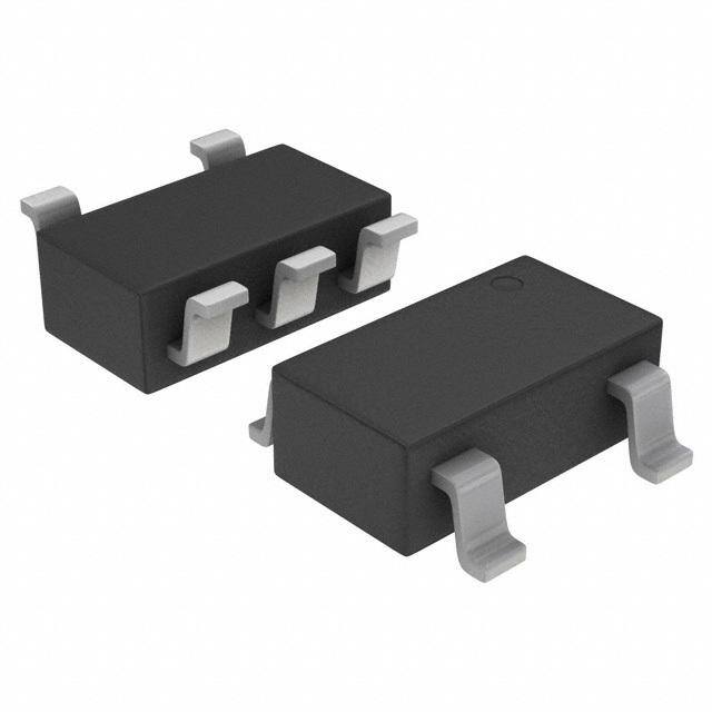
| 描述 | IC REG LDO 5V 0.15A SOT23-5 |
| 产品分类 | |
| 品牌 | ON Semiconductor |
| 数据手册 | |
| 产品图片 |
|
| 产品型号 | NCP4623HSN050T1G |
| rohs | 无铅 / 符合限制有害物质指令(RoHS)规范要求 |
| 产品系列 | - |
| 供应商器件封装 | SOT-23-5 |
| 其它名称 | NCP4623HSN050T1GOSCT |
| 包装 | 剪切带 (CT) |
| 安装类型 | 表面贴装 |
| 封装/外壳 | SC-74A,SOT-753 |
| 工作温度 | -40°C ~ 85°C |
| 标准包装 | 1 |
| 电压-跌落(典型值) | 0.2V @ 20mA |
| 电压-输入 | 最高 24V |
| 电压-输出 | 5V |
| 电流-输出 | 150mA |
| 电流-限制(最小值) | - |
| 稳压器拓扑 | 正,固定式 |
| 稳压器数 | 1 |


- 商务部:美国ITC正式对集成电路等产品启动337调查
- 曝三星4nm工艺存在良率问题 高通将骁龙8 Gen1或转产台积电
- 太阳诱电将投资9.5亿元在常州建新厂生产MLCC 预计2023年完工
- 英特尔发布欧洲新工厂建设计划 深化IDM 2.0 战略
- 台积电先进制程称霸业界 有大客户加持明年业绩稳了
- 达到5530亿美元!SIA预计今年全球半导体销售额将创下新高
- 英特尔拟将自动驾驶子公司Mobileye上市 估值或超500亿美元
- 三星加码芯片和SET,合并消费电子和移动部门,撤换高东真等 CEO
- 三星电子宣布重大人事变动 还合并消费电子和移动部门
- 海关总署:前11个月进口集成电路产品价值2.52万亿元 增长14.8%


PDF Datasheet 数据手册内容提取
NCP4623 150 mA, Wide Input Voltage Range, Low Dropout Regulator The NCP4623 is a CMOS Linear Voltage Regulator designed for wide input voltage range. The maximum operating input voltage is up www.onsemi.com to 24 V with a minimum voltage starting from 2 V. The Chip Enable (CE) pin allows the device to lower standby current to 0.1 (cid:2)A typ. The MARKING NCP4623 features many protections for any current or thermal DIAGRAMS sensitive devices with current fold−back protection, thermal shutdown protection, and peak and short current protection. This device is XXX available in adjustable and fixed voltage output in 0.1 V steps. They XDFN6 XMM are available in very thin XDFN6 1.6x1.6x0.4 mm in size and the very CASE 711AC 1 popular SOT23−5 and SOT89−5 packages. Please contact your local sales office for additional output voltage options. Features 1 • Maximum Operating Input Voltage: 24 V XXX • XZZ Output Voltage Range: 2.5 V to 12.0 V (available in 0.1 V steps) SOT−89 5 2.5 V to 24.0 V (adjustable version) CASE 528AB • Output Voltage Accuracy: ±2.0% • Supply Current: 5 (cid:2)A • Stable with Ceramic Capacitors: 1 (cid:2)F or more XXXM • Current Fold Back Protection SOT−23−5 • Peak and Short Current Protection CASE 1212 1 • Thermal Shutdown Protection • Available in XDFN6 1.6 x 1.6 mm, SOT23−5, SOT89−5 Packages XXX, XXXX= Specific Device Code • M, MM = Date Code These are Pb−Free Devices ZZ = Lot Code Typical Applications • Battery−powered Equipment ORDERING INFORMATION • Networking and Communication Equipment See detailed ordering and shipping information in the package • dimensions section on page 17 of this data sheet. Cameras, DVRs, STB and Camcorders • Home Appliances NCP4623x VIN VOUT VIN VOUT C1 C2 CE 100n 100n GND NCP4623xADJ VIN VOUT VIN VOUT R1 C1 C2 100n CE ADJ 100n GND R2 Figure 1. Typical Application Schematics © Semiconductor Components Industries, LLC, 2016 1 Publication Order Number: January, 2016 − Rev. 4 NCP4623/D
NCP4623 Thermal Thermal Protection Protection VIN VOUT VIN VOUT ADJ Vref Vref Short Peak Current Short Peak Current CE Protection Protection CE Protection Protection GND GND NCP4623Hxxxxx NCP4623HxxADJ Figure 2. Simplified Schematic Block Diagram PIN FUNCTION DESCRIPTION Pin No. XDFN Pin No. Pin No. (Note 1) SOT89−5 SOT23 Pin Name Description 3 1 1 VOUT Output pin 6 2 2 GND Ground 4 3 5 CE Chip enable pin (Active “H”) 1 5 3 VIN Input pin 5 4 4 NC/ADJ No connection (non ADJ versions) / Reference Voltage of Adjustable Output Pin (ADJ versions) 2 − − NC No connection 1. Tab is connected to GND. Tab should be connected to GND, but leaving it unconnected is also acceptable www.onsemi.com 2
NCP4623 ABSOLUTE MAXIMUM RATINGS Rating Symbol Value Unit Input Voltage (Note 2) VIN 26.0 V Output Voltage VOUT −0.3 to VIN + 0.3 V Chip Enable Input VCE −0.3 to VIN + 0.3 V Reference Input Voltage VADJ −0.3 to VIN + 0.3 V Output Current IOUT 250 mA Power Dissipation XDFN6−1616 640 Power Dissipation SOT89−5 PD 900 mW Power Dissipation SOT23−5 420 Junction Temperature T −40 to 150 °C J Operation Temperature TA −40 to 85 °C Storage Temperature T −55 to 125 °C STG ESD Capability, Human Body Model (Note 3) ESD 2000 V HBM ESD Capability, Machine Model (Note 3) ESD 200 V MM Stresses exceeding those listed in the Maximum Ratings table may damage the device. If any of these limits are exceeded, device functionality should not be assumed, damage may occur and reliability may be affected. 2. Refer to ELECTRICAL CHARACTERISTIS and APPLICATION INFORMATION for Safe Operating Area. 3. This device series incorporates ESD protection and is tested by the following methods: ESD Human Body Model tested per AEC−Q100−002 (EIA/JESD22−A114) ESD Machine Model tested per AEC−Q100−003 (EIA/JESD22−A115) Latchup Current Maximum Rating tested per JEDEC standard: JESD78. Latchup Current Maximum Rating tested per JEDEC standard: JESD78. THERMAL CHARACTERISTICS Rating Symbol Value Unit Thermal Characteristics, XDFN6 R(cid:3)JA 156 °C/W Thermal Resistance, Junction−to−Air Thermal Characteristics, SOT23−5 R(cid:3)JA 238 °C/W Thermal Resistance, Junction−to−Air Thermal Characteristics, SOT89−5 R(cid:3)JA 111 °C/W Thermal Resistance, Junction−to−Air ELECTRICAL CHARACTERISTICS NCP4623Hxxxx, CIN = COUT = 0.1 (cid:2)F, TA = +25°C Parameter Test Conditions Symbol Min Typ Max Unit Operating Input Voltage VIN 2 24 V Output Voltage VIN = VOUT(NOM) + 2.0 V, IOUT = 20 mA VOUT x0.98 x1.02 V Output Voltage Temp. Coeffi- VIN = VOUT(NOM) + 2.0 V, IOUT = 20 mA, (cid:4)VOUT/(cid:4)TA ±100 ppm/°C cient −40°C ≤ TA ≤ 105ºC Line Regulation VOUT(NOM) + 1 V ≤ VIN ≤ 24 V, IOUT = 20 mA LineReg 0.05 0.20 %/V Load Regulation VIN = VOUT(NOM) + 2.5 V ≤ VOUT ≤ 3.0 V LoadReg 20 50 2.0 V, IOUT = 1 mA to 40 mA 3.1 V ≤ VOUT ≤ 5.0 V 30 75 mV 5.1 V ≤ VOUT ≤ 12.0 V 40 115 IOUT = 20 mA 2.5 V ≤ VOUT ≤ 7.0 V VDO 0.20 0.40 V Dropout Voltage 7.1 V ≤ VOUT ≤ 10.0 V 0.25 0.50 10.1 V ≤ VOUT ≤ 12.0 V 0.30 0.55 Output Current VIN = VOUT(NOM) + 2.5 V ≤ VOUT ≤ 2.9 V IOUT 140 mA 2.0 V 3.0 V ≤ VOUT ≤ 12.0 V 150 www.onsemi.com 3
NCP4623 ELECTRICAL CHARACTERISTICS NCP4623Hxxxx, CIN = COUT = 0.1 (cid:2)F, TA = +25°C Parameter Test Conditions Symbol Min Typ Max Unit Short Current Limit VOUT = 0 V ISC 45 mA Quiescent Current VIN = VOUT(NOM) + 2.0 V, VCE = VIN IQ 5 10 (cid:2)A Standby Current VIN = 24 V, VCE = 0 V ISTB 0.1 1.0 (cid:2)A CE Pin Threshold Voltage CE Input Voltage “H” VCEH 2.1 VIN V CE Input Voltage “L” VCEL 0 0.3 Power Supply Rejection Ratio VOUT = 3.3V V, VIN = 5.3 V, (cid:4)VIN = 0.2 Vpk−pk, PSRR 35 dB IOUT = 30 mA, f = 1 kHz Output Noise Voltage f = 10 Hz to 100 kHz, VOUT = 3.3 V, VIN = 5.3 V, VN 90 (cid:2)Vrms IOUT = 30 mA Thermal Shutdown Temperature TSD 150 °C Thermal Shutdown Release TSR 125 °C Temperature ELECTRICAL CHARACTERISTICS NCP4623HxxxADJ, VADJ = VOUT, CIN = COUT = 0.1 (cid:2)F, TA = +25°C Parameter Test Conditions Symbol Min Typ Max Unit Operating Input Voltage VIN 2 24 V Output Voltage VIN = VOUT(NOM) + 2.0 V, IOUT = 20 mA VOUT 2.45 2.50 2.55 V Output Voltage Temp. Coeffi- VIN = VOUT(NOM) + 2.0 V, IOUT = 20 mA, (cid:4)VOUT/(cid:4)TA ±100 ppm/°C cient −40°C ≤ TA ≤ 105ºC Line Regulation VOUT(NOM) + 1 V ≤ VIN ≤ 24 V, IOUT = 20 mA LineReg 0.05 0.20 %/V Load Regulation VIN = VOUT(NOM) + 2.0 V, IOUT = 1 mA to 40 mA LoadReg 20 50 mV Dropout Voltage IOUT = 20 mA VDO 0.20 0.40 V Output Current VIN = VOUT(NOM) + 2.0 V IOUT 140 mA Short Current Limit VOUT = 0 V ISC 45 mA 3 Quiescent Current VIN = VOUT(NOM) + 2.0 V, VCE = VIN IQ 5 10 (cid:2)A Standby Current VIN = 24 V, VCE = 0 V ISTB 0.1 1.0 (cid:2)A CE Pin Threshold Voltage CE Input Voltage “H” VCEH 2.1 VIN V CE Input Voltage “L” VCEL 0 0.3 Power Supply Rejection Ratio VIN = 4.5 V, VOUT = 2.5 V, (cid:4)VIN = 0.2 Vpk−pk, PSRR 40 dB IOUT = 30 mA, f = 1 kHz Output Noise Voltage f = 10 Hz to 100 kHz, VOUT = 2.5 V, VIN = 4.5 V, VN 80 (cid:2)Vrms IOUT = 30 mA Thermal Shutdown Temperature TSD 150 °C Thermal Shutdown Release TSR 125 °C Temperature www.onsemi.com 4
NCP4623 TYPICAL CHARACTERISTICS 3.5 3.5 E (V) 3.0 VIN = 4.3 V 7.0 V E (V) 3.0 G 2.5 G 2.5 A A T T L L O 2.0 O 2.0 V V PUT 1.5 6.0 V PUT 1.5 TJ = −40°C 25°C T T U 5.0 V U O 1.0 O 1.0 , UT , UT 105°C O O V 0.5 V 0.5 0.0 0.0 0 50 100 150 200 250 300 0 50 100 150 200 250 300 IOUT, OUTPUT CURRENT (mA) IOUT, OUTPUT CURRENT (mA) Figure 3. Output Voltage vs. Output Current Figure 4. Output Voltage vs. Output Current 3.3 V Version (T = 25(cid:2)C) 3.3 V Version V = 5.3 V J IN 6.0 6.0 V) 5.0 V) 5.0 GE ( GE ( 25°C A 4.0 A 4.0 T T L L O O T V 3.0 T V 3.0 TJ = −40°C PU VIN = 6.5 V PU T T OU 2.0 8.0 V OU 2.0 , T , T U U VO 1.0 7.0 V VO 1.0 105°C 6.0 V 0.0 0.0 0 50 100 150 200 250 300 0 50 100 150 200 250 300 IOUT, OUTPUT CURRENT (mA) IOUT, OUTPUT CURRENT (mA) Figure 5. Output Voltage vs. Output Current Figure 6. Output Voltage vs. Output Current 5.0 V Version (T = 25(cid:2)C) 5.0 V Version V = 7.0 V J IN 14.0 14.0 V)12.0 V)12.0 E ( 15 V E ( G10.0 VIN = 13 V G10.0 A A OLT 8.0 13.5 V OLT 8.0 TJ = −40°C V V T T PU 6.0 14 V PU 6.0 T T OU 4.0 OU 4.0 25°C , T , T U U O O V 2.0 V 2.0 105°C 0.0 0.0 0 50 100 150 200 250 300 0 50 100 150 200 250 300 IOUT, OUTPUT CURRENT (mA) IOUT, OUTPUT CURRENT (mA) Figure 7. Output Voltage vs. Output Current Figure 8. Output Voltage vs. Output Current 12.0 V Version (T = 25(cid:2)C) 12.0 V Version V = 14.0 V J IN www.onsemi.com 5
NCP4623 TYPICAL CHARACTERISTICS 2.0 2.0 V) V) E ( E ( G 1.5 105°C G 1.5 A A T T OL 25°C OL V V 105°C T 1.0 T 1.0 25°C U U O O OP TJ = −40°C OP R R , DO 0.5 , DO 0.5 TJ = −40°C D D V V 0.0 0.0 0 30 60 90 120 150 0 30 60 90 120 150 IOUT, OUTPUT CURRENT (mA) IOUT, OUTPUT CURRENT (mA) Figure 9. Dropout Voltage vs. Output Current Figure 10. Dropout Voltage vs. Output Current 3.3 V Version 5.0 V Version 2.0 3.35 3.34 OLTAGE (V) 1.5 OLTAGE (V) 333...333123 V V UT 1.0 UT 3.30 O P 3.29 ROP 25°C 105°C OUT 3.28 V, DDO 0.5 TJ = −40°C V, OUT 33..2267 0.0 3.25 0 30 60 90 120 150 −40 −20 0 20 40 60 80 100 IOUT, OUTPUT CURRENT (mA) TJ, JUNCTION TEMPERATURE (°C) Figure 11. Dropout Voltage vs. Output Current Figure 12. Output Voltage vs. Temperature, 12.0 V Version 3.3 V Version, V = 5.3 V, I = 20 mA IN OUT 5.05 12.05 5.04 12.04 E (V)5.03 E (V)12.03 G5.02 G12.02 OLTA5.01 OLTA12.01 T V5.00 T V12.00 U U P4.99 P11.99 T T U U O4.98 O11.98 , OUT4.97 , OUT11.97 V4.96 V11.96 4.95 11.95 −40 −20 0 20 40 60 80 100 −40 −20 0 20 40 60 80 100 TJ, JUNCTION TEMPERATURE (°C) TJ, JUNCTION TEMPERATURE (°C) Figure 13. Output Voltage vs. Temperature, Figure 14. Output Voltage vs. Temperature, 5.0 V Version, V = 7.0 V, I = 20 mA 12.0 V Version, V = 14.0 V, I = 20 mA IN OUT IN OUT www.onsemi.com 6
NCP4623 TYPICAL CHARACTERISTICS 8 8 7 7 6 6 5 5 A) A) (cid:2) (cid:2) (D 4 (D 4 N N G G I 3 I 3 2 2 1 1 0 0 0 5 10 15 20 25 0 5 10 15 20 25 VIN, INPUT VOLTAGE (V) VIN, INPUT VOLTAGE (V) Figure 15. Supply Current vs. Input Voltage, Figure 16. Supply Current vs. Input Voltage, 3.3 V Version 5.0 V Version 8 8 7 7 6 6 5 5 A) A) (cid:2) (cid:2) (D 4 (D 4 N N G G I 3 I 3 2 2 1 1 0 0 0 5 10 15 20 25 −40 −20 0 20 40 60 80 100 VIN, INPUT VOLTAGE (V) TJ, JUNCTION TEMPERATURE (°C) Figure 17. Supply Current vs. Input Voltage, Figure 18. Supply Current vs. Temperature, 3.3 V 12.0 V Version Version, V = 5.3 V IN 8 8 7 7 6 6 5 5 A) A) (cid:2) (cid:2) (D 4 (D 4 N N G G I 3 I 3 2 2 1 1 0 0 −40 −20 0 20 40 60 80 100 −40 −20 0 20 40 60 80 100 TJ, JUNCTION TEMPERATURE (°C) TJ, JUNCTION TEMPERATURE (°C) Figure 19. Supply Current vs. Temperature, Figure 20. Supply Current vs. Temperature, 5.0 V Version, V = 7.0 V 12.0 V Version, V = 14.0 V IN IN www.onsemi.com 7
NCP4623 TYPICAL CHARACTERISTICS 3.5 6.0 V) 3.0 V) 5.0 E ( E ( G 2.5 G A A 4.0 T T L L VO 2.0 IOUT = 40 mA VO T T 3.0 PU 1.5 PU IOUT = 40 mA T 20 mA T U U 2.0 O 1.0 O , T , T 20 mA U U VO 0.5 1 mA VO 1.0 1 mA 0.0 0.0 0 5 10 15 20 25 0 5 10 15 20 25 VIN, INPUT VOLTAGE (V) VIN, INPUT VOLTAGE (V) Figure 21. Output Voltage vs. Input Voltage, Figure 22. Output Voltage vs. Input Voltage, 3.3 V Version 5.0 V Version 14.0 70 V) 12.0 60 E ( G 10.0 50 A T T VOL 8.0 R (dB) 40 IOUT = 1 mA U R P 6.0 S 30 30 mA T P OU 4.0 IOUT = 40 mA 20 , T OU 150 mA V 2.0 20 mA 10 1 mA 0.0 0 0 5 10 15 20 25 0.1 1 10 100 1000 VIN, INPUT VOLTAGE (V) FREQUENCY (kHz) Figure 23. Output Voltage vs. Input Voltage, Figure 24. PSRR, 3.3 V Version, V = 6.3 V IN 12.0 V Version 70 70 V) 60 60 E ( G 50 50 A T T VOL 40 30 mAIOUT = 1 mA R (dB) 40 30 mAIOUT = 1 mA U R P 30 S 30 T P U O 20 20 , T U O V 10 150 mA 10 150 mA 0 0 0.1 1 10 100 1000 0.1 1 10 100 1000 VIN, INPUT VOLTAGE (V) FREQUENCY (kHz) Figure 25. PSRR, 5.0 V Version, V = 8.0 V Figure 26. PSRR, 12.0 V Version, V = 15.0 V IN IN www.onsemi.com 8
NCP4623 TYPICAL CHARACTERISTICS 7.0 16 6.0 14 12 5.0 Hz) Hz) 10 √ 4.0 √ /s /s m m 8.0 (cid:2)Vr3.0 (cid:2)Vr (N (N 6.0 V V 2.0 4.0 1.0 2.0 0 0 0.01 0.1 1 10 100 1000 0.01 0.1 1 10 100 1000 FREQUENCY (kHz) FREQUENCY (kHz) Figure 27. Output Voltage Noise, 3.3 V Version, Figure 28. Output Voltage Noise, 5.0 V Version, V = 5.3 V, I = 30 mA V = 7.0 V, I = 30 mA IN OUT IN OUT 45 6.0 40 5.5 35 5.0 4.5 z) 30 H 3.1 (cid:2)√ (V/Nrms 122505 V (V)OUT 22..79 V (V)IN V 2.5 10 2.3 5.0 2.1 0 1.9 0.01 0.1 1 10 100 1000 0 0.1 0.2 0.3 0.4 0.5 0.6 0.7 0.8 0.9 1.0 FREQUENCY (kHz) t (ms) Figure 29. Output Voltage Noise, 12.0 V Version, Figure 30. Line Transients, 2.5 V Version, V = 14.0 V, I = 30 mA t = t = 5 (cid:2)s, I = 30 mA IN OUT R F OUT 6.8 6.3 5.8 5.3 3.9 (V)UT 3.7 (V)N VO 3.5 VI 3.3 3.1 2.9 2.7 0 0.1 0.2 0.3 0.4 0.5 0.6 0.7 0.8 0.9 1.0 t (ms) Figure 31. Line Transients, 3.3 V Version, t = t = 5 (cid:2)s, I = 30 mA R F OUT www.onsemi.com 9
NCP4623 TYPICAL CHARACTERISTICS 8.5 8.0 7.5 7.0 5.6 (V)UT 5.4 (V)N VO 5.2 VI 5.0 4.8 4.6 4.4 0 0.1 0.2 0.3 0.4 0.5 0.6 0.7 0.8 0.9 1.0 t (ms) Figure 32. Line Transients, 5.0 V Version, t = t = 5 (cid:2)s, I = 30 mA R F OUT 15.5 15.0 14.5 14.0 12.6 (V)UT12.4 (V)N VO12.2 VI 12.0 11.8 11.6 11.4 0 0.1 0.2 0.3 0.4 0.5 0.6 0.7 0.8 0.9 1.0 t (ms) Figure 33. Line Transients, 12.0 V Version, t = t = 5 (cid:2)s, I = 30 mA R F OUT 45 30 15 0 V) 3.1 A) (UT 2.9 (mT O U V 2.7 O I 2.5 2.3 2.1 1.9 0 0.4 0.8 1.2 1.6 2.0 2.4 2.8 3.2 3.6 4.0 t (ms) Load Transients, 2.5 V Version, I = 1 - OUT 30 mA, t = t = 50 (cid:2)s, V = 4.5 V R F IN www.onsemi.com 10
NCP4623 TYPICAL CHARACTERISTICS 45 30 15 0 3.9 V) A) (UT 3.7 (mT O 3.5 U V O I 3.3 3.1 2.9 2.7 0 0.4 0.8 1.2 1.6 2.0 2.4 2.8 3.2 3.6 4.0 t (ms) Figure 34 - Load Transients, 3.3 V Version, I = 1 - 30 mA, t = t = 50 (cid:2)s, V = 5.3 V OUT R F IN 45 30 15 0 V) 5.6 A) (UT 5.4 (mT O U V 5.2 O I 5.0 4.8 4.6 4.4 0 0.4 0.8 1.2 1.6 2.0 2.4 2.8 3.2 3.6 4.0 t (ms) Figure 35. Load Transients, 5.0 V Version, I = 1 − 30 mA, t = t = 50 (cid:2)s, V = 7.0 V OUT R F IN 45 30 15 0 V)12.6 A) (UT12.4 (mT O U V12.2 O I 12.0 11.8 11.6 11.4 0 0.4 0.8 1.2 1.6 2.0 2.4 2.8 3.2 3.6 4.0 t (ms) Figure 36. Load Transients, 12.0 V Version, I = 1 − 30 mA, t = t = 50 (cid:2)s, V = 14.0 V OUT R F IN www.onsemi.com 11
NCP4623 TYPICAL CHARACTERISTICS 150 100 50 0 V) 4.0 A) (UT 3.5 (mT O U V 3.0 O I 2.5 2.0 1.5 1.0 0 0.4 0.8 1.2 1.6 2.0 2.4 2.8 3.2 3.6 4.0 t (ms) Figure 37. Load Transients, 2.5 V Version, I = 1 − 100 mA, t = t = 50 (cid:2)s, V = 4.5 V OUT R F IN 150 100 50 0 V) 4.8 A) (UT 4.3 (mT O U V 3.8 O I 3.3 2.8 2.3 1.8 0 0.4 0.8 1.2 1.6 2.0 2.4 2.8 3.2 3.6 4.0 t (ms) Figure 38. Load Transients, 3.3 V Version, I = 1 − 100 mA, t = t = 50 (cid:2)s, V = 5.3 V OUT R F IN 150 100 50 0 V) 6.5 A) (UT 6.0 (mT O U V 5.5 O I 5.0 4.5 4.0 3.5 0 0.4 0.8 1.2 1.6 2.0 2.4 2.8 3.2 3.6 4.0 t (ms) Figure 39. Load Transients, 5.0 V Version, I = 1 − 100 mA, t = t = 50 (cid:2)s, V = 7.0 V OUT R F IN www.onsemi.com 12
NCP4623 TYPICAL CHARACTERISTICS 150 100 50 0 V) 13.5 A) (UT 13.0 (mT O U V 12.5 O I 12.0 11.5 11.0 10.5 0 0.4 0.8 1.2 1.6 2.0 2.4 2.8 3.2 3.6 4.0 t (ms) Figure 40. Load Transients, 12.0 V Version, I = 1 − 100 mA, t = t = 50 (cid:2)s, V = 14.0 V OUT R F IN 6.75 Chip Enable 4.50 2.25 0 V) 2.5 IOUT = 1 mA V) V (OUT 12..50 IOUT = 150 mA V (CE 1.0 0.5 IOUT = 30 mA 0 −0.5 0 0.1 0.2 0.3 0.4 0.5 0.6 0.7 0.8 0.9 1.0 t ((cid:2)s) Figure 41. Start−up, 2.5 V Version, V = 4.5 V IN 7.95 Chip Enable 5.30 2.65 0 V) V) V (OUT 34..00 IOUT = 1 mA V (CE 2.0 IOUT = 150 mA 1.0 0 IOUT = 30 mA −1.0 0 0.1 0.2 0.3 0.4 0.5 0.6 0.7 0.8 0.9 1.0 t ((cid:2)s) Figure 42. Start−up, 3.3 V Version, V = 5.3 V IN www.onsemi.com 13
NCP4623 TYPICAL CHARACTERISTICS 10.50 Chip Enable 7.00 3.50 0 5.0 V (V)OUT 34..00 IOUT = 1 mA IOUT = 150 mA V (V)CE 2.0 1.0 0 IOUT = 30 mA −1.0 0 0.1 0.2 0.3 0.4 0.5 0.6 0.7 0.8 0.9 1.0 t ((cid:2)s) Figure 43. Start−up, 5.0 V Version, V = 7.0 V IN 21 Chip Enable 14 7 0 V) V) V (OUT192..00 IOUT = 1 mA V (CE 6.0 IOUT = 30 mA 3.0 0 IOUT = 150 mA −3.0 0 0.1 0.2 0.3 0.4 0.5 0.6 0.7 0.8 0.9 1.0 t ((cid:2)s) Figure 45. Start−up, 12.0 V Version, V = 14.0 V IN 6.75 4.50 2.25 Chip Enable 0 2.5 V) V) V (OUT 12..50 IOUT = 1 mA V (CE 1.0 IOUT = 30 mA 0.5 0 −0.5 IOUT = 150 mA 0 0.1 0.2 0.3 0.4 0.5 0.6 0.7 0.8 0.9 1.0 t (ms) Figure 44. Shutdown, 2.5 V Version, V = 4.5 V IN www.onsemi.com 14
NCP4623 TYPICAL CHARACTERISTICS 7.95 5.30 2.65 Chip Enable 0 V) V) V (OUT 34..00 IOUT = 1 mA V (CE 2.0 IOUT = 30 mA 1.0 0 IOUT = 150 mA −1.0 0 0.1 0.2 0.3 0.4 0.5 0.6 0.7 0.8 0.9 1.0 t (ms) Figure 46. Shutdown, 3.3 V Version, V = 5.3 V IN 10.5 7.0 3.5 Chip Enable 0 5.0 V) V) V (OUT 34..00 IOUT = 1 mA V (CE 2.0 IOUT = 30 mA 1.0 0 IOUT = 150 mA −1.0 0 0.1 0.2 0.3 0.4 0.5 0.6 0.7 0.8 0.9 1.0 t (ms) Figure 47. Shutdown, 5.0 V Version, V = 7.0 V IN 21 14 7 Chip Enable 0 V (V)OUT192..00 IOUT = 1 mA V (V)CE 6.0 IOUT = 30 mA 3.0 0 IOUT = 150 mA −3.0 0 0.1 0.2 0.3 0.4 0.5 0.6 0.7 0.8 0.9 1.0 t (ms) Figure 48. Shutdown, 12.0 V Version, V = 14.0 V IN www.onsemi.com 15
NCP4623 APPLICATION INFORMATION A typical application circuits for NCP4623 series is of voltage divider low enough to achieve cross current shown in Figure 49. around 2 (cid:2)A to eliminate error. Output voltage can be computed from the equation: NCP4623x (cid:3) (cid:5) VIN VOUT R1 VIN VOUT VOUT(cid:2)2.5 1(cid:4)R2 (cid:4)R1(cid:6)IADJ (eq. 1) C1 C2 CE 100n 100n GND Enable Operation The enable pin CE may be used for turning the regulator on and off. The IC is switched on when a high level voltage is applied to the CE pin. Do not leave the CE pin unconnected or between VCEH and VCEL voltage levels as NCP4623xADJ this may leave the output voltage unstable or cause indefinite VIN VOUT VIN VOUT and unexpected currents flows internally. R1 C1 C2 100n CE ADJ 100n Current Limit GND R2 This regulator includes a fold−back type current limit circuit. This type of protection doesn’t limit output current up to specified current capability in normal operation, but when an over current occurs, output voltage and current decrease until the over current condition ends. Typical Figure 49. Typical Application Schematics characteristics of this protection type can be observed in the Output Voltage vs. Output Current graphs shown in the typical characteristics section of this datasheet. Input Decoupling Capacitor (C1) A 0.1 (cid:2)F ceramic input decoupling capacitor should be Thermal connected as close as possible to the input and ground pin of As power across the IC increase, it might become the NCP4623. Higher values and lower ESR improves line necessary to provide some thermal relief. The maximum transient response. power dissipation supported by the device is dependent upon board design and layout. Mounting pad configuration Output Decoupling Capacitor (C2) on the PCB, the board material, and also the ambient Recommended values of the ceramic output decoupling temperature affect the rate of temperature increase for the capacitor is in the range from 0.1 (cid:2)F to 2.2 (cid:2)F. Stable part. When the device has good thermal conductivity operation of the regulator should be achieved within this through the PCB the junction temperature will be relatively range. If a tantalum capacitor is used, and its ESR is high, low in high power dissipation applications. loop oscillation may result. The capacitors should be The IC includes internal thermal shutdown circuit that connected as close as possible to the output and ground pins. stops operation of regulator, if junction temperature is Larger values and lower ESR improves dynamic higher than 150°C. After that, when junction temperature parameters. decreases below 125°C, the operation of voltage regulator Output Voltage Setting (ADJ version) will resume. During high power dissipation condition, the The output voltage of the adjustable regulator may be set regulator shuts down and resumes repeatedly protecting for any output voltage from its voltage reference (2.5 V) up itself from overheating. to V voltage by an external voltage divider connected IN PCB layout between VOUT and GND pins with its center connected to Make the V and GND line as large as practical. If their the ADJ pin. The voltage divider is loaded by current into IN impedance is high, noise pickup or unstable operation may ADJ pin that is typically around 200 nA. This current may result. Connect capacitors C1 and C2 as close as possible to cause an error in V , therefore it is good to choose values OUT the IC, and make wiring as short as possible. www.onsemi.com 16
NCP4623 ORDERING INFORMATION Nominal Output Device Voltage Description Marking Package Shipping† NCP4623HSNADJT1G Adjustable Enable high J24 NCP4623HSN050T1G 5.0 V Enable high J50 SOT23−5 3000 / Tape & Reel (Pb−Free) NCP4623HSN100T1G 10.0 V Enable high J00 NCP4623HSN120T1G 12.0 V Enable high J20 NCP4623HMXADJTCG Adjustable Enable high BQ24 NCP4623HMX025TCG 2.5 V Enable high BQ25 NCP4623HMX033TCG 3.3 V Enable high BQ33 XDFN1616−6 NCP4623HMX045TCG 4.5 V Enable high BQ45 5000 / Tape & Reel (Pb−Free) NCP4623HMX048TCG 4.8 V Enable high BQ48 NCP4623HMX050TCG 5.0 V Enable high BQ50 NCP4623HMX080TCG 8.0 V Enable high BQ80 †For information on tape and reel specifications, including part orientation and tape sizes, please refer to our Tape and Reel Packaging Specifications Brochure, BRD8011/D. *To order other package and voltage variants, please contact your ON Semiconductor sales representative. www.onsemi.com 17
NCP4623 PACKAGE DIMENSIONS XDFN6 1.6x1.6, 0.5P CASE 711AC ISSUE O D A NOTES: 1. DIMENSIONING AND TOLERANCING PER 2X B ASME Y14.5M, 1994. 0.05 C 2. CONTROLLING DIMENSION: MILLIMETERS. 3. COPLANARITY APPLIES TO THE EXPOSED PAD AS WELL AS THE TERMINALS. ÉÉÉ PIN ONE E MILLIMETERS REFERENCE ÉÉÉ DIM MIN MAX A −−− 0.40 A1 0.00 0.05 2X b 0.15 0.25 0.05 C D 1.60 BSC D2 1.25 1.35 TOP VIEW E 1.60 BSC E2 0.65 0.75 A E3 0.15 REF 0.05 C A1 e 0.50 BSC L 0.15 0.25 L1 0.05 BSC 0.05 C NOTE 3 SIDE VIEW C SPELAATNIENG RECOMMENDED MOUNTING FOOTPRINT* 0.05 M C A B 1.70 D2 L 1 3 2X L1 E2 6X 0.38 0.77 1.79 0.05 M C A B 3XE3 6 4 PACKAGE 6Xb OUTLINE 1 e 0.05 M C A B 0.50 BOTTOM VIEW PITCH 6X 0.36 DIMENSIONS: MILLIMETERS *For additional information on our Pb−Free strategy and soldering details, please download the ON Semiconductor Soldering and Mounting Techniques Reference Manual, SOLDERRM/D. www.onsemi.com 18
NCP4623 PACKAGE DIMENSIONS SOT−89, 5 LEAD CASE 528AB ISSUE O D NOTES: 1. DIMENSIONING AND TOLERANCING PER ASME Y14.5M, 1994. 2. CONTROLLING DIMENSION: MILLIMETERS. 3. LEAD THICKNESS INCLUDES LEAD FINISH. 4. DIMENSIONS D AND E DO NOT INCLUDE MOLD FLASH, PROTRUSIONS, OR GATE BURRS. E H 5. DIMENSIONS L, L2, L3, L4, L5, AND H ARE MEAS- URED AT DATUM PLANE C. MILLIMETERS DIM MIN MAX 1 A 1.40 1.60 b 0.32 0.52 b1 0.37 0.57 TOP VIEW c 0.30 0.50 D 4.40 4.60 D2 1.40 1.80 E 2.40 2.60 c e 1.40 1.60 A H 4.25 4.45 L 1.10 1.50 0.10 C L2 0.80 1.20 L3 0.95 1.35 C SIDE VIEW L4 0.65 1.05 L5 0.20 0.60 e e RECOMMENDED b1 b L2 MOUNTING FOOTPRINT* L 1 2 3 4X0.57 1.75 1.50 L5 0.45 2.79 5 4 4.65 L3 L4 D2 1.65 BOTTOM VIEW 1.30 1 2X 0.62 2X1.50 DIMENSIONS: MILLIMETERS *For additional information on our Pb−Free strategy and soldering details, please download the ON Semiconductor Soldering and Mounting Techniques Reference Manual, SOLDERRM/D. www.onsemi.com 19
NCP4623 PACKAGE DIMENSIONS SOT−23 5−LEAD CASE 1212 ISSUE A NOTES: A 1. DIMENSIONING AND TOLERANCING PER ASME Y14.5M, 1994. A D B A2 2. CONTROLLING DIMENSIONS: MILLIMETERS. 0.05 S A1 3. DATUM C IS THE SEATING PLANE. MILLIMETERS 5 4 DIM MIN MAX E L A --- 1.45 1 2 3 A1 0.00 0.10 E1 A2 1.00 1.30 L1 5Xb C b 0.30 0.50 c 0.10 0.25 e 0.10 M C B S A S C D 2.70 3.10 E 2.50 3.10 E1 1.50 1.80 e 0.95 BSC RECOMMENDED L 0.20 --- SOLDERING FOOTPRINT* L1 0.45 0.75 3.30 5X 0.85 5X 0.56 0.95 PITCH DIMENSIONS: MILLIMETERS *For additional information on our Pb−Free strategy and soldering details, please download the ON Semiconductor Soldering and Mounting Techniques Reference Manual, SOLDERRM/D. ON Semiconductor and the are registered trademarks of Semiconductor Components Industries, LLC (SCILLC) or its subsidiaries in the United States and/or other countries. SCILLC owns the rights to a number of patents, trademarks, copyrights, trade secrets, and other intellectual property. A listing of SCILLC’s product/patent coverage may be accessed at www.onsemi.com/site/pdf/Patent−Marking.pdf. SCILLC reserves the right to make changes without further notice to any products herein. SCILLC makes no warranty, representation or guarantee regarding the suitability of its products for any particular purpose, nor does SCILLC assume any liability arising out of the application or use of any product or circuit, and specifically disclaims any and all liability, including without limitation special, consequential or incidental damages. “Typical” parameters which may be provided in SCILLC data sheets and/or specifications can and do vary in different applications and actual performance may vary over time. All operating parameters, including “Typicals” must be validated for each customer application by customer’s technical experts. SCILLC does not convey any license under its patent rights nor the rights of others. SCILLC products are not designed, intended, or authorized for use as components in systems intended for surgical implant into the body, or other applications intended to support or sustain life, or for any other application in which the failure of the SCILLC product could create a situation where personal injury or death may occur. Should Buyer purchase or use SCILLC products for any such unintended or unauthorized application, Buyer shall indemnify and hold SCILLC and its officers, employees, subsidiaries, affiliates, and distributors harmless against all claims, costs, damages, and expenses, and reasonable attorney fees arising out of, directly or indirectly, any claim of personal injury or death associated with such unintended or unauthorized use, even if such claim alleges that SCILLC was negligent regarding the design or manufacture of the part. SCILLC is an Equal Opportunity/Affirmative Action Employer. This literature is subject to all applicable copyright laws and is not for resale in any manner. PUBLICATION ORDERING INFORMATION LITERATURE FULFILLMENT: N. American Technical Support: 800−282−9855 Toll Free ON Semiconductor Website: www.onsemi.com Literature Distribution Center for ON Semiconductor USA/Canada 19521 E. 32nd Pkwy, Aurora, Colorado 80011 USA Europe, Middle East and Africa Technical Support: Order Literature: http://www.onsemi.com/orderlit Phone: 303−675−2175 or 800−344−3860 Toll Free USA/Canada Phone: 421 33 790 2910 Fax: 303−675−2176 or 800−344−3867 Toll Free USA/Canada Japan Customer Focus Center For additional information, please contact your local Email: orderlit@onsemi.com Phone: 81−3−5817−1050 Sales Representative www.onsemi.com NCP4623/D 20
Mouser Electronics Authorized Distributor Click to View Pricing, Inventory, Delivery & Lifecycle Information: O N Semiconductor: NCP4623HMX045TCG NCP4623HMX048TCG NCP4623HMX050TCG NCP4623HMXADJTCG NCP4623HSN050T1G NCP4623HSN120T1G