ICGOO在线商城 > 集成电路(IC) > PMIC - 配电开关,负载驱动器 > NCP45560IMNTWG-H
 Datasheet下载
- 型号: NCP45560IMNTWG-H
- 制造商: ON Semiconductor
- 库位|库存: xxxx|xxxx
- 要求:
| 数量阶梯 | 香港交货 | 国内含税 |
| +xxxx | $xxxx | ¥xxxx |
查看当月历史价格
查看今年历史价格
NCP45560IMNTWG-H产品简介:
ICGOO电子元器件商城为您提供NCP45560IMNTWG-H由ON Semiconductor设计生产,在icgoo商城现货销售,并且可以通过原厂、代理商等渠道进行代购。 NCP45560IMNTWG-H价格参考。ON SemiconductorNCP45560IMNTWG-H封装/规格:PMIC - 配电开关,负载驱动器, Power Switch/Driver 1:1 N-Channel 24A 12-DFN (3x3)。您可以下载NCP45560IMNTWG-H参考资料、Datasheet数据手册功能说明书,资料中有NCP45560IMNTWG-H 详细功能的应用电路图电压和使用方法及教程。
NCP45560IMNTWG-H是安森美(ON Semiconductor)推出的一款高效率、低压同步降压型DC-DC转换器,属于PMIC中的配电开关与负载驱动器类别。该器件主要面向便携式电子设备和低功耗系统,适用于对空间和能效要求较高的应用场景。

典型应用包括:智能手机、平板电脑、可穿戴设备(如智能手表和健康监测设备)、物联网(IoT)终端节点、无线传感器网络以及电池供电的嵌入式系统。其宽输入电压范围(2.7V至5.5V)支持单节锂离子/锂聚合物电池供电,输出电压可调,最大输出电流可达6A,适合为处理器、FPGA、ASIC等核心负载提供稳定的电源。

此外,该芯片采用小型化封装(如QFN),集成度高,配合外部少量元件即可实现紧凑的电源设计,有助于减小PCB面积。其支持脉冲频率调制(PFM)和脉宽调制(PWM)模式切换,在轻载时提升效率,延长电池续航时间。具备过温保护、过流保护等安全功能,确保系统稳定运行。

综上,NCP45560IMNTWG-H广泛应用于需要高效、小型化、长续航的便携式电子产品中,是现代低功耗系统电源管理的理想选择。
| 参数 | 数值 |
| 产品目录 | 集成电路 (IC)半导体 |
| 描述 | IC REG LDO电源开关 IC - 配电 NCP45560IMNTWG-H |
| 产品分类 | PMIC - 电源分配开关集成电路 - IC |
| 品牌 | ON Semiconductor |
| 产品手册 | |
| 产品图片 | |
| rohs | 符合RoHS无铅 / 符合限制有害物质指令(RoHS)规范要求 |
| 产品系列 | 开关 IC,电源开关 IC - 配电,ON Semiconductor NCP45560IMNTWG-HecoSWITCH™ |
| mouser_ship_limit | 该产品可能需要其他文件才能进口到中国。 |
| 数据手册 | |
| 产品型号 | NCP45560IMNTWG-H |
| Rds(On) | 5.1 毫欧 |
| 产品 | Load Switches |
| 产品种类 | 电源开关 IC - 配电 |
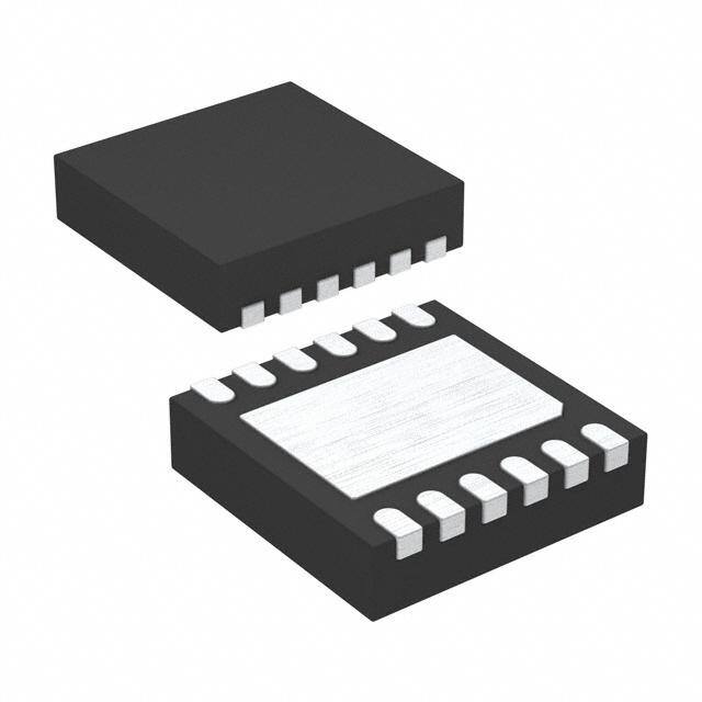
| 供应商器件封装 | 12-DFN(3x3) |
| 其它名称 | NCP45560IMNTWG-HOSDKR |
| 内部开关 | 是 |
| 包装 | Digi-Reel® |
| 商标 | ON Semiconductor |
| 安装类型 | 表面贴装 |
| 安装风格 | SMD/SMT |
| 导通电阻—最大值 | 3.2 mOhms |
| 封装 | Reel |
| 封装/外壳 | 12-VFDFN 裸露焊盘 |
| 封装/箱体 | DFN-12 |
| 工作温度 | -40°C ~ 85°C |
| 工作电源电压 | 3.3 V |
| 工厂包装数量 | 3000 |
| 最大功率耗散 | 3.49 W |
| 最大工作温度 | + 85 C |
| 最小工作温度 | - 40 C |
| 标准包装 | 1 |
| 电压-输入 | 0.5 V ~ 13.5 V |
| 电流限制 | 24A |
| 电源电流—最大值 | 24 A |
| 空闲时间—最大值 | 0.8 us |
| 类型 | 高端 |
| 系列 | NCP45560 |
| 输出数 | 1 |
| 输出端数量 | 1 |
| 运行时间—最大值 | 265 us |


- 商务部:美国ITC正式对集成电路等产品启动337调查
- 曝三星4nm工艺存在良率问题 高通将骁龙8 Gen1或转产台积电
- 太阳诱电将投资9.5亿元在常州建新厂生产MLCC 预计2023年完工
- 英特尔发布欧洲新工厂建设计划 深化IDM 2.0 战略
- 台积电先进制程称霸业界 有大客户加持明年业绩稳了
- 达到5530亿美元!SIA预计今年全球半导体销售额将创下新高
- 英特尔拟将自动驾驶子公司Mobileye上市 估值或超500亿美元
- 三星加码芯片和SET,合并消费电子和移动部门,撤换高东真等 CEO
- 三星电子宣布重大人事变动 还合并消费电子和移动部门
- 海关总署:前11个月进口集成电路产品价值2.52万亿元 增长14.8%


PDF Datasheet 数据手册内容提取
NCP45560 (cid:2) ecoSWITCH Advanced Load Management Controlled Load Switch with Low R ON The NCP45560 load switch provides a component and area-reducing solution for efficient power domain switching with www.onsemi.com inrush current limit via soft−start. In addition to integrated control functionality with ultra low on−resistance, this device offers system RON TYP VCC VIN IMAX safeguards and monitoring via fault protection and power good 4.1 m(cid:2) 3.3 V 1.8 V signaling. This cost effective solution is ideal for power management and hot-swap applications requiring low power consumption in a 4.3 m(cid:2) 3.3 V 5.0 V 24 A small footprint. 4.9 m(cid:2) 3.3 V 12 V Features • Advanced Controller with Charge Pump • Integrated N-Channel MOSFET with Ultra Low R ON • Input Voltage Range 0.5 V to 13.5 V • Soft-Start via Controlled Slew Rate 1 • Adjustable Slew Rate Control DFN12, 3x3 • Power Good Signal CASE 506CD • Thermal Shutdown • Undervoltage Lockout MARKING DIAGRAM • Short-Circuit Protection NCP45 • Extremely Low Standby Current 560−x • ALYW(cid:2) Load Bleed (Quick Discharge) (cid:2) • This is a Pb−Free Device Typical Applications x = H for NCP45560−H • = L for NCP45560−L Portable Electronics and Systems A = Assembly Location • Notebook and Tablet Computers L = Wafer Lot • Y = Year Telecom, Networking, Medical, and Industrial Equipment W = Work Week • Set−Top Boxes, Servers, and Gateways (cid:2) = Pb−Free Package • Hot−Swap Devices and Peripheral Ports (Note: Microdot may be in either location) VCC EN PG VIN PIN CONFIGURATION VIN 1 12 VOUT Thermal, Bandgap Undervoltage EN 2 11 VOUT Control & & Biases Logic Short−Circuit VCC 3 10 VOUT Protection 13: VIN GND 4 9 VOUT SR 5 8 VOUT Delay and Charge Slew Rate PG 6 7 BLEED Pump Control (Top View) ORDERING INFORMATION SR GND BLEED VOUT See detailed ordering and shipping information on page12 of Figure 1. Block Diagram this data sheet. © Semiconductor Components Industries, LLC, 2015 1 Publication Order Number: May, 2018 − Rev. 4 NCP45560/D
NCP45560 Table 1. PIN DESCRIPTION Pin Name Function 1, 13 VIN Drain of MOSFET (0.5 V – 13.5 V), Pin 1 must be connected to Pin 13 2 EN NCP45560−H − Active−high digital input used to turn on the MOSFET, pin has an internal pull down resistor to GND NCP45560−L − Active−low digital input used to turn on the MOSFET, pin has an internal pull up resistor to VCC 3 VCC Supply voltage to controller (3.0 V − 5.5 V) 4 GND Controller ground 5 SR Slew rate adjustment; float if not used 6 PG Active−high, open−drain output that indicates when the gate of the MOSFET is fully charged, external pull up resistor ≥ 1 k(cid:2) to an external voltage source required; tie to GND if not used. 7 BLEED Load bleed connection, must be tied to VOUT either directly or through a resistor ≤ 1 k(cid:2) 8−12 VOUT Source of MOSFET connected to load Table 2. ABSOLUTE MAXIMUM RATINGS Rating Symbol Value Unit Supply Voltage Range VCC −0.3 to 6 V Input Voltage Range VIN −0.3 to 18 V Output Voltage Range VOUT −0.3 to 18 V EN Digital Input Range VEN −0.3 to (VCC + 0.3) V PG Output Voltage Range (Note 1) VPG −0.3 to 6 V Thermal Resistance, Junction−to−Ambient, Steady State (Note 2) RθJA 28.6 °C/W Thermal Resistance, Junction−to−Ambient, Steady State (Note 3) RθJA 49.7 °C/W Thermal Resistance, Junction−to−Case (VIN Paddle) RθJC 1.7 °C/W Continuous MOSFET Current @ TA = 25°C (Notes 2 and 4) IMAX 24 A Continuous MOSFET Current @ TA = 25°C (Notes 3 and 4) IMAX 18.3 A Total Power Dissipation @ TA = 25°C (Note 2) PD 3.49 W Derate above TA = 25°C 34.9 mW/°C Total Power Dissipation @ TA = 25°C (Note 3) PD 2.01 W Derate above TA = 25°C 20.1 mW/°C Storage Temperature Range TSTG −40 to 150 °C Lead Temperature, Soldering (10 sec.) TSLD 260 °C ESD Capability, Human Body Model (Notes 5 and 6) ESDHBM 3.0 kV ESD Capability, Machine Model (Note 5) ESDMM 200 V ESD Capability, Charged Device Model (Note 5) ESDCDM 1.0 kV Latch−up Current Immunity (Notes 5 and 6) LU 100 mA Stresses exceeding those listed in the Maximum Ratings table may damage the device. If any of these limits are exceeded, device functionality should not be assumed, damage may occur and reliability may be affected. 1. PG is an open−drain output that requires an external pull up resistor ≥ 1 k(cid:2) to an external voltage source. 2. Surface−mounted on FR4 board using 1 sq−in pad, 1 oz Cu. 3. Surface−mounted on FR4 board using the minimum recommended pad size, 1 oz Cu. 4. Ensure that the expected operating MOSFET current will not cause the Short−Circuit Protection to turn the MOSFET off undesirably. 5. Tested by the following methods @ TA = 25°C: ESD Human Body Model tested per JESD22−A114 ESD Machine Model tested per JESD22−A115 ESD Charged Device Model per ESD STM5.3.1 Latch−up Current tested per JESD78 6. Rating is for all pins except for VIN and VOUT which are tied to the internal MOSFET’s Drain and Source. Typical MOSFET ESD performance for VIN and VOUT should be expected and these devices should be treated as ESD sensitive. www.onsemi.com 2
NCP45560 Table 3. OPERATING RANGES Rating Symbol Min Max Unit Supply Voltage VCC 3 5.5 V Input Voltage VIN 0.5 13.5 V Ground GND 0 V Ambient Temperature TA −40 85 °C Junction Temperature TJ −40 125 °C Table 4. ELECTRICAL CHARACTERISTICS (TJ = 25°C unless otherwise specified) Parameter Conditions (Note 7) Symbol Min Typ Max Unit MOSFET On−Resistance VCC = 3.3 V; VIN = 1.8 V RON 4.1 5.0 m(cid:2) VCC = 3.3 V; VIN = 5 V 4.3 5.3 VCC = 3.3 V; VIN = 12 V 4.9 6.8 Leakage Current (Note 8) VEN = 0 V; VIN = 13.5 V ILEAK 0.1 1.0 (cid:3)A CONTROLLER Supply Standby Current (Note 9) VEN = 0 V; VCC = 3 V ISTBY 0.65 2.0 (cid:3)A VEN = 0 V; VCC = 5.5 V 3.2 4.5 Supply Dynamic Current (Note 10) VEN = VCC = 3 V; VIN = 12 V IDYN 280 400 (cid:3)A VEN = VCC = 5.5 V; VIN = 1.8 V 530 750 Bleed Resistance VEN = 0 V; VCC = 3 V RBLEED 86 115 144 (cid:2) VEN = 0 V; VCC = 5.5 V 72 97 121 Bleed Pin Leakage Current VEN = VCC = 3 V, VIN = 1.8 V IBLEED 6.0 10 (cid:3)A VEN = VCC = 3 V, VIN = 12 V 60 70 EN Input High Voltage VCC = 3 V − 5.5 V VIH 2.0 V EN Input Low Voltage VCC = 3 V − 5.5 V VIL 0.8 V EN Input Leakage Current NCP45560−H; VEN = 0 V IIL 90 500 nA NCP45560−L; VEN = VCC IIH 90 500 EN Pull Down Resistance NCP45560−H RPD 76 100 124 k(cid:2) EN Pull Up Resistance NCP45560−L RPU 76 100 124 k(cid:2) PG Output Low Voltage (Note 11) VCC = 3 V; ISINK = 5 mA VOL 0.2 V PG Output Leakage Current (Note 12) VCC = 3 V; VTERM = 3.3 V IOH 5.0 100 nA Slew Rate Control Constant (Note 13) VCC = 3 V KSR 26 33 40 (cid:3)A FAULT PROTECTIONS Thermal Shutdown Threshold (Note 14) VCC = 3 V − 5.5 V TSDT 145 °C Thermal Shutdown Hysteresis (Note 14) VCC = 3 V − 5.5 V THYS 20 °C VIN Undervoltage Lockout Threshold VCC = 3 V VUVLO 0.25 0.35 0.45 V VIN Undervoltage Lockout Hysteresis VCC = 3 V VHYS 25 40 60 mV Short−Circuit Protection Threshold VCC = 3 V; VIN = 0.5 V VSC 200 265 350 mV VCC = 3 V; VIN = 13.5 V 100 285 500 7. VEN shown only for NCP45560−H, (EN Active−High) unless otherwise specified. 8. Average current from VIN to VOUT with MOSFET turned off. 9. Average current from VCC to GND with MOSFET turned off. 10.Average current from VCC to GND after charge up time of MOSFET. 11.PG is an open-drain output that is pulled low when the MOSFET is disabled. 12.PG is an open-drain output that is not driven when the gate of the MOSFET is fully charged, requires an external pull up resistor ≥ 1 k(cid:2) to an external voltage source, VTERM. 13.See Applications Information section for details on how to adjust the slew rate. 14.Operation above TJ = 125°C is not guaranteed. Product parametric performance is indicated in the Electrical Characteristics for the listed test conditions, unless otherwise noted. Product performance may not be indicated by the Electrical Characteristics if operated under different conditions. www.onsemi.com 3
NCP45560 Table 5. SWITCHING CHARACTERISTICS (TJ = 25°C unless otherwise specified) (Notes 15 and 16) Parameter Conditions Symbol Min Typ Max Unit Output Slew Rate VCC = 3.3 V; VIN = 1.8 V SR 12.4 kV/s VCC = 5.0 V; VIN = 1.8 V 12.6 VCC = 3.3 V; VIN = 12 V 13.7 VCC = 5.0 V; VIN = 12 V 14.0 Output Turn−on Delay VCC = 3.3 V; VIN = 1.8 V TON 195 (cid:3)s VCC = 5.0 V; VIN = 1.8 V 180 VCC = 3.3 V; VIN = 12 V 280 VCC = 5.0 V; VIN = 12 V 265 Output Turn−off Delay VCC = 3.3 V; VIN = 1.8 V TOFF 4.1 (cid:3)s VCC = 5.0 V; VIN = 1.8 V 3.5 VCC = 3.3 V; VIN = 12 V 1.4 VCC = 5.0 V; VIN = 12 V 0.8 Power Good Turn−on Time VCC = 3.3 V; VIN = 1.8 V TPG,ON 1.71 ms VCC = 5.0 V; VIN = 1.8 V 1.08 VCC = 3.3 V; VIN = 12 V 2.15 VCC = 5.0 V; VIN = 12 V 1.35 Power Good Turn−off Time VCC = 3.3 V; VIN = 1.8 V TPG,OFF 28 ns VCC = 5.0 V; VIN = 1.8 V 21 VCC = 3.3 V; VIN = 12 V 28 VCC = 5.0 V; VIN = 12 V 21 15.See below figure for Test Circuit and Timing Diagram. 16.Tested with the following conditions: VTERM = VCC; RPG = 100 k(cid:2); RL = 10 (cid:2); CL = 0.1 (cid:3)F. VTERM RPG OFF ON EN PG VIN NCP45560−H VOUT VCC BLEED RL CL SR GND 50% 50% VEN TON (cid:4)t TOFF 90% 90% (cid:4)V SR = (cid:4)V VOUT 10% (cid:4)t TPG,ON TPG,OFF 50% 50% VPG Figure 2. Switching Characteristics Test Circuit and Timing Diagrams www.onsemi.com 4
NCP45560 TYPICAL CHARACTERISTICS (TJ = 25°C unless otherwise specified) 5.5 7.5 (cid:2)m) 55..13 VVCCCC == 53. 5V V (cid:2)m) 67..50 VCC = 3.3 V VIN = 12 V E ( 4.9 E ( C C 6.0 N N A 4.7 A VIN = 5.0 V T T 5.5 S S SI 4.5 SI E E 5.0 R 4.3 R N− N− 4.5 VIN = 1.8 V O 4.1 O , ON 3.9 , ON 4.0 R R 3.7 3.5 3.5 3.0 0.5 2.5 4.5 6.5 8.5 10.5 12.5 −45 −30 −15 0 15 30 45 60 75 90 105 120 VIN, INPUT VOLTAGE (V) TJ, JUNCTION TEMPERATURE (°C) Figure 3. On−Resistance vs. Input Voltage Figure 4. On−Resistance vs. Temperature A) 3.5 A) 7 (cid:3) (cid:3) T ( T ( N N 6 E 3.0 E R R R R 5 U U C 2.5 C Y Y B B 4 D D TAN 2.0 TAN 3 VCC = 5.5 V S S Y 1.5 Y PL PL 2 P P U U , SY 1.0 , SY 1 VCC = 3 V B B ST 0.5 ST 0 I 3.0 3.5 4.0 4.5 5.0 5.5 I −45 −30−15 0 15 30 45 60 75 90 105 120 VCC, SUPPLY VOLTAGE (V) TJ, JUNCTION TEMPERATURE (°C) Figure 5. Supply Standby Current vs. Supply Figure 6. Supply Standby Current vs. Voltage Temperature A) 550 A) 600 (cid:3) (cid:3) T ( 500 T ( 550 N N E E R 450 R 500 CUR CUR 450 VIN = 1.8 V C 400 C MI MI 400 A 350 A N N 350 Y Y Y D 300 VCC = 5.5 V Y D 300 PL 250 PL VIN = 12 V P P 250 U U , SN 200 VCC = 3 V , SN 200 Y Y D 150 D 150 I 0.5 2.5 4.5 6.5 8.5 10.5 12.5 I 3.0 3.5 4.0 4.5 5.0 5.5 VIN, INPUT VOLTAGE (V) VCC, SUPPLY VOLTAGE (V) Figure 7. Supply Dynamic Current vs. Input Figure 8. Supply Dynamic Current vs. Supply Voltage Voltage www.onsemi.com 5
NCP45560 TYPICAL CHARACTERISTICS (TJ = 25°C unless otherwise specified) A) 700 115 (cid:3) T ( 650 VCC = 5.5 V, VIN = 1.8 V (cid:2)) RREN 600 NCE ( 110 U 550 TA C S C 500 SI MI E NA 450 D R 105 Y 400 E D E PLY 350 , BLD 100 P 300 E U E , SN 250 VCC = 3.0 V, VIN = 12 V RBL DY 200 95 I −45 −15 15 45 75 105 3.0 3.5 4.0 4.5 5.0 5.5 TJ, JUNCTION TEMPERATURE (°C) VCC, SUPPLY VOLTAGE (V) Figure 9. Supply Dynamic Current vs. Figure 10. Bleed Resistance vs. Supply Temperature Voltage 145 70 (cid:2)) E ( 135 GE 60 C A VCC = 3 V AN VCC = 3 V AK 50 ED RESIST 111255 VCC = 5.5 V EED PIN LE(cid:3)RRENT (A) 3400 VCC = 5.5 V E LU , BLD 105 , BEDC 20 E E E 95 L L B 10 B I R 85 0 −45 −15 15 45 75 105 0.5 2.5 4.5 6.5 8.5 10.5 12.5 TJ, JUNCTION TEMPERATURE (°C) VIN, INPUT VOLTAGE (V) Figure 11. Bleed Resistance vs. Temperature Figure 12. Bleed Pin Leakage Current vs. Input Voltage A) (cid:2)) (cid:3) 80 k 120 T ( E ( N C RE 70 VCC = 3 V, VIN = 12 V AN 115 R T U 60 S C SI 110 E E G 50 R A P 105 K U EA 40 N/ L W 100 N 30 O D PI 20 LL D 95 E U E P BL 10 VCC = 3 V, VIN = 1.8 V N 90 , ED 0 , EU 85 E P IBL −45 −1T5J, JUNC1T5ION TEM4P5ERATUR75E (°C) 105 IPD/ −45 −1T5J, JUNC1T5ION TEM4P5ERATUR75E (°C) 105 Figure 13. Bleed Pin Leakage Current vs. Figure 14. EN Pull Down/Up Resistance vs. Temperature Temperature www.onsemi.com 6
NCP45560 TYPICAL CHARACTERISTICS (TJ = 25°C unless otherwise specified) 0.140 0.20 E (V) ISINK = 5 mA E (V) ISINK = 5 mA G0.135 G 0.18 A A LT LT VCC = 3 V O O V0.130 V 0.16 W W O O L0.125 L 0.14 UT UT VCC = 5.5 V P P T0.120 T 0.12 U U O O G G P0.115 P 0.10 , L , L O O V V 0.110 0.08 3.0 3.5 4.0 4.5 5.0 5.5 −45 −15 15 45 75 105 VCC, SUPPLY VOLTAGE (V) TJ, JUNCTION TEMPERATURE (°C) Figure 15. PG Output Low Voltage vs. Supply Figure 16. PG Output Low Voltage vs. Voltage Temperature A) A) (cid:3) 37 (cid:3) 35.5 T ( T ( N 36 N STA 35 VCC = 5.5 V STA35.0 VCC = 5.5 V N N O O34.5 C 34 C ROL 33 VCC = 3 V ROL 34.0 T T N N O 32 O33.5 C C E 31 E VCC = 3 V T T33.0 A A R 30 R W W 32.5 E 29 E L L S S , R 28 , R32.0 S 0.5 2.5 4.5 6.5 8.5 10.5 12.5 S −45 −15 15 45 75 105 K K VIN, INPUT VOLTAGE (V) TJ, JUNCTION TEMPERATURE (°C) Figure 17. Slew Rate Control Constant vs. Figure 18. Slew Rate Control Constant vs. Input Voltage Temperature 320 14.5 N CTIO 310 V/s) 14.0 VCC = 5.5 V OTEV)300 VCC = 5.5 V TE (k 1133..05 VCC = 3 V Rm A T PD (290 W R 12.5 RCUIHOL VCC = 3 V SLE 12.0 CIES280 T 11.5 −R U ORTTH270 UTP 11.0 H O 10.5 , SC 260 SR, 10.0 S V 250 9.5 0.5 2.5 4.5 6.5 8.5 10.5 12.5 0.5 2.5 4.5 6.5 8.5 10.5 12.5 VIN, INPUT VOLTAGE (V) VIN, INPUT VOLTAGE (V) Figure 19. Short−Circuit Protection Threshold Figure 20. Output Slew Rate vs. Input Voltage vs. Input Voltage www.onsemi.com 7
NCP45560 TYPICAL CHARACTERISTICS (TJ = 25°C unless otherwise specified) 14.0 310 V/s) VCC = 3.3 V, VIN = 12 V (cid:3)Y (s) 290 E (k 13.5 ELA 270 VCC = 3 V T D EW RA 13.0 N−ON 250 VCC = 5.5 V L R 230 S U PUT 12.5 VCC = 5 V, VIN = 1.8 V UT T 210 T P U T 190 SR, O 12.0 , OUN 170 O T 11.5 150 −40 −20 0 20 40 60 80 100 120 0.5 2.5 4.5 6.5 8.5 10.5 12.5 TJ, JUNCTION TEMPERATURE (°C) VIN, INPUT VOLTAGE (V) Figure 21. Output Slew Rate vs. Temperature Figure 22. Output Turn−on Delay vs. Input Voltage s) 300 (cid:3)s) 7 (cid:3)Y ( 275 VCC = 3.3 V, VIN = 12 V AY ( 6 A L L E N DE 250 FF D 5 O O − − 4 N N R 225 R VCC = 3 V U U T T 3 T T U 200 U TP TP 2 VCC = 5.5 V OU 175 VCC = 5 V, VIN = 1.8 V OU T, ON 150 T, OFF 01 −40 −20 0 20 40 60 80 100 120 0.5 2.5 4.5 6.5 8.5 10.5 12.5 TJ, JUNCTION TEMPERATURE (°C) VIN, INPUT VOLTAGE (V) Figure 23. Output Turn−on Delay vs. Figure 24. Output Turn−off Delay vs. Input Temperature Voltage s) 4.5 4.0 (cid:3) AY ( 4.0 ms) 3.5 EL VCC = 5 V, VIN = 1.8 V E ( F D 3.5 TIM 3.0 OF ON VCC = 3 V UT TURN− 32..05 G TURN− 22..05 UTP 2.0 , PON 1.5 VCC = 5.5 V , OF 1.5 VCC = 3.3 V, VIN = 12 V PG, 1.0 F T O T 1.0 0.5 −40 −20 0 20 40 60 80 100 120 0.5 2.5 4.5 6.5 8.5 10.5 12.5 TJ, JUNCTION TEMPERATURE (°C) VIN, INPUT VOLTAGE (V) Figure 25. Output Turn−off Delay vs. Figure 26. Power Good Turn−on Time vs. Input Temperature Voltage www.onsemi.com 8
NCP45560 TYPICAL CHARACTERISTICS (TJ = 25°C unless otherwise specified) 2.8 32 E (ms) 22..46 ME (ns) 30 VIN = 13.5 V N TIM 2.2 VCC = 3.3 V, VIN = 12 V FF TI 28 O 2.0 O 26 − − RN 1.8 RN VIN = 0.5 V U U 24 T 1.6 T G G , PG,ON 11..24 VCC = 5 V, VIN = 1.8 V , PG,OFF 2202 TP 1.0 TP 0.8 18 −40 −20 0 20 40 60 80 100 120 3.0 3.5 4.0 4.5 5.0 5.5 TJ, JUNCTION TEMPERATURE (°C) VCC, SUPPLY VOLTAGE (V) Figure 27. Power Good Turn−on Time vs. Figure 28. Power Good Turn−off Time vs. Temperature Supply Voltage 35.0 s) E (n 32.5 M VCC = 3.3 V, VIN = 12 V TI 30.0 F F O 27.5 − N R U 25.0 T G , PF22.5 VCC = 5 V, VIN = 1.8 V F O G,20.0 P T 17.5 −40 −20 0 20 40 60 80 100 120 TJ, JUNCTION TEMPERATURE (°C) Figure 29. Power Good Turn−off Time vs. Temperature www.onsemi.com 9
NCP45560 APPLICATIONS INFORMATION Enable Control The power good output can be used as the enable signal for The NCP45560 has two part numbers, NCP45560−H and other active−high devices in the system (as shown in NCP45560−L, that only differ in the polarity of the enable Figure 32). This allows for guaranteed by design power control. sequencing and reduces the number of enable signals needed The NCP45560−H device allows for enabling the from the system controller. If the power good feature is not MOSFET in an active−high configuration. When the VCC used in the application, the PG pin should be tied to GND. supply pin has an adequate voltage applied and the EN pin is at a logic high level, the MOSFET will be enabled. Slew Rate Control Similarly, when the EN pin is at a logic low level, the The NCP45560 devices are equipped with controlled output slew rate which provides soft start functionality. This MOSFET will be disabled. An internal pull down resistor to limits the inrush current caused by capacitor charging and ground on the EN pin ensures that the MOSFET will be enables these devices to be used in hot swap applications. disabled when not being driven. The slew rate can be decreased with an external capacitor The NCP45560−L device allows for enabling the added between the SR pin and ground (as shown in MOSFET in an active−low configuration. When the V CC supply pin has an adequate voltage applied and the EN pin Figures 30 and 31). With an external capacitor present, the is at a logic low level, the MOSFET will be enabled. slew rate can be determined by the following equation: Similarly, when the EN pin is at a logic high level, the K SlewRate(cid:2) SR [V(cid:3)s] (eq. 1) MOSFET will be disabled. An internal pull up resistor to C SR V on the EN pin ensures that the MOSFET will be CC where K is the specified slew rate control constant, found disabled when not being driven. SR in Table 4, and C is the slew rate control capacitor added SR Power Sequencing between the SR pin and ground. The slew rate of the device The NCP45560 devices will function with any power will always be the lower of the default slew rate and the sequence, but the output turn−on delay performance may adjusted slew rate. Therefore, if the C is not large enough SR vary from what is specified. To achieve the specified to decrease the slew rate more than the specified default performance, there are two recommended power sequences: value, the slew rate of the device will be the default value. 1.V → V → V The SR pin can be left floating if the slew rate does not need CC IN EN 2.V → V → V to be decreased. IN CC EN Load Bleed (Quick Discharge) Short−Circuit Protection The NCP45560 devices have an internal bleed resistor, The NCP45560 devices are equipped with short−circuit R , which is used to bleed the charge off of the load to protection that is used to help protect the part and the system BLEED ground after the MOSFET has been disabled. In series with from a sudden high−current event, such as the output, V , OUT the bleed resistor is a bleed switch that is enabled whenever being shorted to ground. This circuitry is only active when the MOSFET is disabled. The MOSFET and the bleed the gate of the MOSFET is fully charged. switch are never concurrently active. Once active, the circuitry monitors the difference in the It is required that the BLEED pin be connected to V voltage on the V pin and the voltage on the BLEED pin. OUT IN either directly (as shown in Figure 31) or through an external In order for the V voltage to be monitored through the OUT resistor, R (as shown in Figure 30). R should not BLEED pin, it is required that the BLEED pin be connected EXT EXT exceed 1 k(cid:2) and can be used to increase the total bleed to V either directly (as shown in Figure 31) or through OUT resistance. a resistor, R (as shown in Figure 30), which should not EXT Care must be taken to ensure that the power dissipated exceed 1 k(cid:2). With the BLEED pin connected to V , the OUT across R is kept at a safe level. The maximum short−circuit protection is able to monitor the voltage drop BLEED continuous power that can be dissipated across R is across the MOSFET. BLEED 0.4 W. R can be used to decrease the amount of power If the voltage drop across the MOSFET is greater than or EXT dissipated across R . equal to the short−circuit protection threshold voltage, the BLEED MOSFET is immediately turned off and the load bleed is Power Good activated. The part remains latched in this off state until EN The NCP45560 devices have a power good output (PG) is toggled or V supply voltage is cycled, at which point the CC that can be used to indicate when the gate of the MOSFET MOSFET will be turned on in a controlled fashion with the is fully charged. The PG pin is an active−high, open−drain normal output turn−on delay and slew rate. The current output that requires an external pull up resistor, R , greater PG through the MOSFET that will cause a short−circuit event than or equal to 1 k(cid:2) to an external voltage source, V , TERM can be calculated by dividing the short−circuit protection compatible with input levels of other devices connected to threshold by the expected on−resistance of the MOSFET. this pin (as shown in Figures 30 and 31). www.onsemi.com 10
NCP45560 Thermal Shutdown Undervoltage Lockout The thermal shutdown of the NCP45560 devices protects The undervoltage lockout of the NCP45560 devices turns the part from internally or externally generated excessive the MOSFET off and activates the load bleed when the input temperatures. This circuitry is disabled when EN is not voltage, V , is less than or equal to the undervoltage IN active to reduce standby current. When an over−temperature lockout threshold. This circuitry is disabled when EN is not condition is detected, the MOSFET is immediately turned active to reduce standby current. off and the load bleed is activated. If the V voltage rises above the undervoltage lockout IN The part comes out of thermal shutdown when the threshold, and EN remains active, the MOSFET will be junction temperature decreases to a safe operating turned on in a controlled fashion with the normal output temperature as dictated by the thermal hysteresis. Upon turn−on delay and slew rate. exiting a thermal shutdown state, and if EN remains active, the MOSFET will be turned on in a controlled fashion with the normal output turn−on delay and slew rate. V = 3.3 V TERM Power Supply or Battery R PG 100 k(cid:2) 3.0 V − 5.5 V 0.5 V − 13.5 V Controller VCC EN PG VIN Thermal, Bandgap Control Undervoltage & & Logic Biases Short−Circuit Protection Delay and Charge Slew Rate Pump Control R D D T S N E U G E VO L CSR B R EXT Load Figure 30. Typical Application Diagram − Load Switch www.onsemi.com 11
NCP45560 VCC EN PG VTERM GND VIN 3.0 V − 5.5 V 0.5 V − 13.5 V R PG BACKPLANE REMOVABLE CARD VCC EN PG VIN Thermal, Bandgap Undervoltage Control & & Logic Biases Short−Circuit Protection Delay and Charge Slew Rate Pump Control R D D UT S N E O G E V C L SR B Load Figure 31. Typical Application Diagram − Hot Swap V = 3.3 V TERM R PG Controller 10 k(cid:2) N G N G E P E P R R PD PD 100 k(cid:2) 100 k(cid:2) PG PG NCP45560−H NCP45560−H Figure 32. Simplified Application Diagram − Power Sequencing with PG Output ORDERING INFORMATION Device EN Polarity Package Shipping† NCP45560IMNTWG−H Active−High DFN12 3000 / Tape & Reel NCP45560IMNTWG−L Active−Low (Pb−Free) †For information on tape and reel specifications, including part orientation and tape sizes, please refer to our Tape and Reel Packaging Specifications Brochure, BRD8011/D. www.onsemi.com 12
NCP45560 PACKAGE DIMENSIONS DFN12 3x3, 0.5P CASE 506CD ISSUE A NOTES: D A B L L 1. DIMENSIONING AND TOLERANCING PER ASME Y14.5M, 1994. 2. CONTROLLING DIMENSION: MILLIMETERS. L1 3. DIMENSION b APPLIES TO PLATED TERMINAL AND IS MEASURED BETWEEN DETAIL A 0.15 AND 0.30 MM FROM TERMINAL TIP. 4. COPLANARITY APPLIES TO THE EXPOSED INDPICINA OTONRE ÇÇÇ E COANLSTTERRUNCATTIOENS PAD AS WELL AS THE TERMINALS. MILLIMETERS ÇÇÇ DIM MIN MAX A 0.80 1.00 2X 0.10 C ÇÇÇ MOLD CMPD A1 0.00 0.05 EXPOSED Cu A3 0.20 REF 2X 0.10 C TOP VIEW ÇÇ Db 0.32.000 BS0C.30 ÉÉ D2 2.60 2.80 0.05 C DETAIL B A3 E 3.00 BSC A1 A3 E2 1.90 2.10 e 0.50 BSC A DETAIL B L 0.20 0.40 ALTERNATE L1 −−− 0.15 0.05 C CONSTRUCTION L2 0.10 REF A1 K 0.15 MIN NOTE 4 SIDE VIEW C SPELAATNIENG RECOMMENDED SOLDERING FOOTPRINT* 0.10 M C A B 2.86 DETAIL A D2 12X L 011.X32 1 6 0.10 M C A B L2 12X 0.48 E2 2.10 3.30 PACKAGE OUTLINE K 12 7 12Xb e 0.10 M C A-B B 1 e/2 0.05 M C NOTE 3 0.45 0.50 BOTTOM VIEW PITCH DIMENSIONS: MILLIMETERS *For additional information on our Pb−Free strategy and soldering details, please download the ON Semiconductor Soldering and Mounting Techniques Reference Manual, SOLDERRM/D. ecoSWITCH is a trademark of Semiconductor Components Industries, LLC (SCILLC). ON Semiconductor and are trademarks of Semiconductor Components Industries, LLC dba ON Semiconductor or its subsidiaries in the United States and/or other countries. ON Semiconductor owns the rights to a number of patents, trademarks, copyrights, trade secrets, and other intellectual property. A listing of ON Semiconductor’s product/patent coverage may be accessed at www.onsemi.com/site/pdf/Patent−Marking.pdf. ON Semiconductor reserves the right to make changes without further notice to any products herein. ON Semiconductor makes no warranty, representation or guarantee regarding the suitability of its products for any particular purpose, nor does ON Semiconductor assume any liability arising out of the application or use of any product or circuit, and specifically disclaims any and all liability, including without limitation special, consequential or incidental damages. Buyer is responsible for its products and applications using ON Semiconductor products, including compliance with all laws, regulations and safety requirements or standards, regardless of any support or applications information provided by ON Semiconductor. “Typical” parameters which may be provided in ON Semiconductor data sheets and/or specifications can and do vary in different applications and actual performance may vary over time. All operating parameters, including “Typicals” must be validated for each customer application by customer’s technical experts. ON Semiconductor does not convey any license under its patent rights nor the rights of others. ON Semiconductor products are not designed, intended, or authorized for use as a critical component in life support systems or any FDA Class 3 medical devices or medical devices with a same or similar classification in a foreign jurisdiction or any devices intended for implantation in the human body. Should Buyer purchase or use ON Semiconductor products for any such unintended or unauthorized application, Buyer shall indemnify and hold ON Semiconductor and its officers, employees, subsidiaries, affiliates, and distributors harmless against all claims, costs, damages, and expenses, and reasonable attorney fees arising out of, directly or indirectly, any claim of personal injury or death associated with such unintended or unauthorized use, even if such claim alleges that ON Semiconductor was negligent regarding the design or manufacture of the part. ON Semiconductor is an Equal Opportunity/Affirmative Action Employer. This literature is subject to all applicable copyright laws and is not for resale in any manner. PUBLICATION ORDERING INFORMATION LITERATURE FULFILLMENT: N. American Technical Support: 800−282−9855 Toll Free ON Semiconductor Website: www.onsemi.com Literature Distribution Center for ON Semiconductor USA/Canada 19521 E. 32nd Pkwy, Aurora, Colorado 80011 USA Europe, Middle East and Africa Technical Support: Order Literature: http://www.onsemi.com/orderlit Phone: 303−675−2175 or 800−344−3860 Toll Free USA/Canada Phone: 421 33 790 2910 Fax: 303−675−2176 or 800−344−3867 Toll Free USA/Canada For additional information, please contact your local Email: orderlit@onsemi.com Sales Representative ◊ www.onsemi.com NCP45560/D 13
Mouser Electronics Authorized Distributor Click to View Pricing, Inventory, Delivery & Lifecycle Information: O N Semiconductor: NCP45560IMNTWG-H