ICGOO在线商城 > 集成电路(IC) > 逻辑 - 缓冲器,驱动器,接收器,收发器 > NC7WZ17P6
 Datasheet下载
- 型号: NC7WZ17P6
- 制造商: Fairchild Semiconductor
- 库位|库存: xxxx|xxxx
- 要求:
| 数量阶梯 | 香港交货 | 国内含税 |
| +xxxx | $xxxx | ¥xxxx |
查看当月历史价格
查看今年历史价格
NC7WZ17P6产品简介:
ICGOO电子元器件商城为您提供NC7WZ17P6由Fairchild Semiconductor设计生产,在icgoo商城现货销售,并且可以通过原厂、代理商等渠道进行代购。 NC7WZ17P6价格参考¥0.88-¥1.75。Fairchild SemiconductorNC7WZ17P6封装/规格:逻辑 - 缓冲器,驱动器,接收器,收发器, Buffer, Non-Inverting 2 Element 1 Bit per Element Push-Pull Output SC-70-6。您可以下载NC7WZ17P6参考资料、Datasheet数据手册功能说明书,资料中有NC7WZ17P6 详细功能的应用电路图电压和使用方法及教程。
ON Semiconductor的NC7WZ17P6属于逻辑IC中的缓冲器/驱动器类别,是一款双路施密特触发缓冲器,具有高噪声抑制能力。该器件广泛应用于需要信号整形和增强驱动能力的数字电路中。

其主要应用场景包括:

1. 信号调理:用于清理带有噪声或抖动的输入信号,提升信号完整性;
2. 接口电路:在不同电压域之间进行电平转换和缓冲,确保信号稳定传输;
3. 时钟分配系统:对时钟信号进行缓冲和驱动,提高时钟网络的稳定性;
4. 工业控制设备:如PLC、传感器模块等,用于增强控制信号的驱动能力和抗干扰性能;
5. 通信设备:用于数据线路的缓冲与驱动,保障高速数据传输的可靠性;
6. 消费电子产品:如智能家电、穿戴设备中,用于逻辑信号处理与驱动。

该器件采用微型6引脚封装,适用于空间受限的设计,且支持宽工作温度范围,适合工业级应用需求。
| 参数 | 数值 |
| 产品目录 | 集成电路 (IC)半导体 |
| 描述 | IC BUFF DL SCHMT TRIG UHS SC706缓冲器和线路驱动器 UHS Dual Buffer w/Schmitt Trigger |
| 产品分类 | |
| 品牌 | Fairchild Semiconductor |
| 产品手册 | |
| 产品图片 |
|
| rohs | 符合RoHS无铅 / 符合限制有害物质指令(RoHS)规范要求 |
| 产品系列 | 逻辑集成电路,缓冲器和线路驱动器,Fairchild Semiconductor NC7WZ17P67WZ |
| 数据手册 | |
| 产品型号 | NC7WZ17P6 |
| PCN封装 | |
| PCN设计/规格 | |
| 产品种类 | 缓冲器和线路驱动器 |
| 传播延迟时间 | 6.6 ns at 3.3 V, 5.6 ns at 5 V |
| 低电平输出电流 | 32 mA |
| 供应商器件封装 | SC-70-6 |
| 元件数 | 2 |
| 其它名称 | NC7WZ17P6CT |
| 包装 | 剪切带 (CT) |
| 单位重量 | 28 mg |
| 商标 | Fairchild Semiconductor |
| 安装类型 | 表面贴装 |
| 安装风格 | SMD/SMT |
| 封装 | Reel |
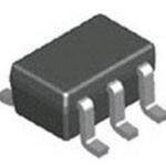
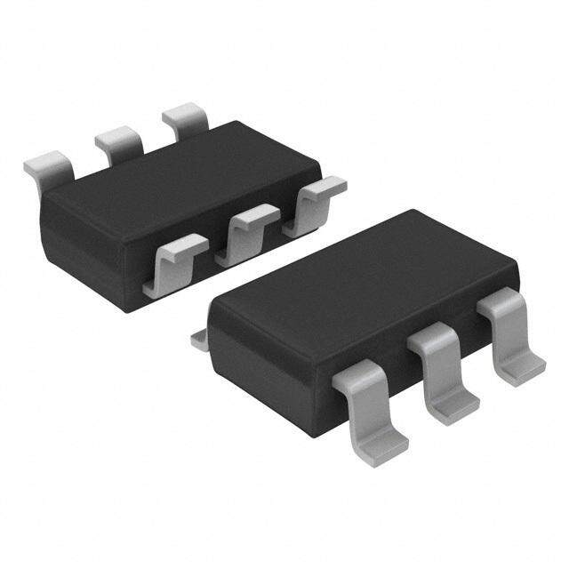
| 封装/外壳 | 6-TSSOP,SC-88,SOT-363 |
| 封装/箱体 | SC-70-6 |
| 工作温度 | -40°C ~ 85°C |
| 工厂包装数量 | 250 |
| 最大功率耗散 | 180 mW |
| 最大工作温度 | + 85 C |
| 最小工作温度 | - 40 C |
| 极性 | Non-Inverting |
| 标准包装 | 1 |
| 每元件位数 | 1 |
| 每芯片的通道数量 | 2 |
| 电压-电源 | 1.65 V ~ 5.5 V |
| 电流-输出高,低 | 32mA,32mA |
| 电源电压-最大 | 5.5 V |
| 电源电压-最小 | 1.65 V |
| 系列 | NC7WZ17 |
| 输入线路数量 | 2 |
| 输出线路数量 | 2 |
| 逻辑类型 | CMOS |
| 逻辑系列 | TinyLogic UHS |
| 零件号别名 | NC7WZ17P6_NL |
| 高电平输出电流 | - 32 mA |


- 商务部:美国ITC正式对集成电路等产品启动337调查
- 曝三星4nm工艺存在良率问题 高通将骁龙8 Gen1或转产台积电
- 太阳诱电将投资9.5亿元在常州建新厂生产MLCC 预计2023年完工
- 英特尔发布欧洲新工厂建设计划 深化IDM 2.0 战略
- 台积电先进制程称霸业界 有大客户加持明年业绩稳了
- 达到5530亿美元!SIA预计今年全球半导体销售额将创下新高
- 英特尔拟将自动驾驶子公司Mobileye上市 估值或超500亿美元
- 三星加码芯片和SET,合并消费电子和移动部门,撤换高东真等 CEO
- 三星电子宣布重大人事变动 还合并消费电子和移动部门
- 海关总署:前11个月进口集成电路产品价值2.52万亿元 增长14.8%


PDF Datasheet 数据手册内容提取
Is Now Part of To learn more about ON Semiconductor, please visit our website at www.onsemi.com Please note: As part of the Fairchild Semiconductor integration, some of the Fairchild orderable part numbers will need to change in order to meet ON Semiconductor’s system requirements. Since the ON Semiconductor product management systems do not have the ability to manage part nomenclature that utilizes an underscore (_), the underscore (_) in the Fairchild part numbers will be changed to a dash (-). This document may contain device numbers with an underscore (_). Please check the ON Semiconductor website to verify the updated device numbers. The most current and up-to-date ordering information can be found at www.onsemi.com. Please email any questions regarding the system integration to Fairchild_questions@onsemi.com. ON Semiconductor and the ON Semiconductor logo are trademarks of Semiconductor Components Industries, LLC dba ON Semiconductor or its subsidiaries in the United States and/or other countries. ON Semiconductor owns the rights to a number of patents, trademarks, copyrights, trade secrets, and other intellectual property. A listing of ON Semiconductor’s product/patent coverage may be accessed at www.onsemi.com/site/pdf/Patent-Marking.pdf. ON Semiconductor reserves the right to make changes without further notice to any products herein. ON Semiconductor makes no warranty, representation or guarantee regarding the suitability of its products for any particular purpose, nor does ON Semiconductor assume any liability arising out of the application or use of any product or circuit, and specifically disclaims any and all liability, including without limitation special, consequential or incidental damages. Buyer is responsible for its products and applications using ON Semiconductor products, including compliance with all laws, regulations and safety requirements or standards, regardless of any support or applications information provided by ON Semiconductor. “Typical” parameters which may be provided in ON Semiconductor data sheets and/or specifications can and do vary in different applications and actual performance may vary over time. All operating parameters, including “Typicals” must be validated for each customer application by customer’s technical experts. ON Semiconductor does not convey any license under its patent rights nor the rights of others. ON Semiconductor products are not designed, intended, or authorized for use as a critical component in life support systems or any FDA Class 3 medical devices or medical devices with a same or similar classification in a foreign jurisdiction or any devices intended for implantation in the human body. Should Buyer purchase or use ON Semiconductor products for any such unintended or unauthorized application, Buyer shall indemnify and hold ON Semiconductor and its officers, employees, subsidiaries, affiliates, and distributors harmless against all claims, costs, damages, and expenses, and reasonable attorney fees arising out of, directly or indirectly, any claim of personal injury or death associated with such unintended or unauthorized use, even if such claim alleges that ON Semiconductor was negligent regarding the design or manufacture of the part. ON Semiconductor is an Equal Opportunity/Affirmative Action Employer. This literature is subject to all applicable copyright laws and is not for resale in any manner.
N C 7 W Z January 2012 1 7 — T i n y NC7WZ17 L o g TinyLogic® UHS Dual Buffer with Schmitt Trigger Inputs i c ® U H S D Features Description u a Ultra-High Speed: t 3.6ns (Typical) into 50pF The NC7WZ17 is a dual buffer with Schmitt trigger l PD B at 5V VCC inputs from Fairchild's Ultra-High Speed (UHS) series u of TinyLogic® products. The device is fabricated with f High Output Drive: ±24mA at 3V VCC advanced CMOS technology to achieve ultra-high fe r Broad V Operating Range: 1.65V to 5.5V speed with high output drive, while maintaining low w CC Matches Performance of LCX when Operated sotpaetirca tinpgo wrearn ged.is sTihpea tidoenv icoev eirs sap evceifriey d btroo aodp erVaCteC ith at 3.3V VCC over the 1.65V to 5.5V VCC range. The inputs and S c Power Down High Impedance Inputs/Outputs outputs are high-impedance when VCC is 0V. Inputs h Over-Voltage Tolerance Inputs Facilitate 5V to 3V toopleerraattein g vovoltaltaggees . Supc hmtoit t 7trVig, geinr dienppeuntsd eanct hieovf e V1CVC mi t Translation typical hysteresis between the positive- and negative- t T Proprietary Noise/EMI Reduction Circuitry going input threshold voltage at 5V. r i g Ultra-Small MicroPak™ Packages g e Space-Saving SC70 Package r I n p u t s Ordering Information Operating Packing Part Number Top Mark Package Temperature Method 3000 Units on NC7WZ17P6X -40 to +85°C Z17 6-Lead SC70, EIAJ SC-88a, 1.25mm Wide Tape & Reel 5000 Units on NC7WZ17L6X -40 to +85°C A5 6-Lead MicroPak™, 1.00mm Wide Tape & Reel 5000 Units on NC7WZ17FHX -40 to +85°C A5 6-Lead, MicroPak2, 1x1mm Body, .35mm Pitch Tape & Reel © 1999 Fairchild Semiconductor Corporation www.fairchildsemi.com NC7WZ17 • Rev. 1.0.6
N C Connection Diagrams 7 W IEEC/IEC Z 1 7 A 1 Y 1 1 — T A Y i 2 2 n y L o Figure 1. Logic Symbol g i c ® Pin Configurations U H S D A1 1 6 Y1 A1 1 6 Y1 u a l GND 2 5 VCC GND 2 5 VCC B u f f A2 3 4 Y2 A2 3 4 Y2 er w i Figure 2. SC70 (Top View) Figure 3. MicroPak (Top Through View) th S c h m AAA i t t T r i g Pin One g e r Notes: I n 1. AAA represents Product Code Top Mark (see ordering code). p 2. Orientation of Top Mark determines Pin One location. Read the top product code mark left to right. u t Pin One is the lower left pin. s Figure 4. SC70 Pin 1 Orientation Pin Definitions Pin # SC70 Pin # MicroPak Name Description 1 1 A Input 1 2 2 GND Ground 3 3 A Input 2 4 4 Y Output 2 5 5 V Supply Voltage CC 6 6 Y Output 1 Function Table Y = A Inputs Output A Y L L H H H = HIGH Logic Level L = LOW Logic Level © 1999 Fairchild Semiconductor Corporation www.fairchildsemi.com NC7WZ17 • Rev. 1.0.6 2
N C Absolute Maximum Ratings 7 W Stresses exceeding the absolute maximum ratings may damage the device. The device may not function or be Z operable above the recommended operating conditions and stressing the parts to these levels is not recommended. 1 7 In addition, extended exposure to stresses above the recommended operating conditions may affect device reliability. — The absolute maximum ratings are stress ratings only. T Symbol Parameter Min. Max. Unit in y V Supply Voltage -0.5 7.0 V L CC o V DC Input Voltage -0.5 7.0 V g IN i c V DC Output Voltage -0.5 7.0 V ® OUT U I DC Input Diode Current V < -0.5V -50 mA IK IN H I DC Output Diode Current V < -0.5V -50 mA S OK OUT D I DC Output Current ±50 mA OUT u a ICC or IGND DC VCC or Ground Current ±100 mA l B TSTG Storage Temperature Range -65 +150 °C u f T Junction Temperature Under Bias +150 °C f J e r T Junction Lead Temperature (Soldering, 10 Seconds) +260 °C L w SC70-6 180 it h PD Power Dissipation at 85°C MicroPak-6 130 mW S c MicroPak2-6 120 h m Human Body Model, JEDEC:JESD22-A114 4000 i ESD V t t Charge Device Model, JEDEC:JESD22-C101 2000 T r i g g e r I n Recommended Operating Conditions(3) p u t The Recommended Operating Conditions table defines the conditions for actual device operation. Recommended s operating conditions are specified to ensure optimal performance to the datasheet specifications. Fairchild does not recommend exceeding them or designing to Absolute Maximum Ratings. Symbol Parameter Conditions Min. Max. Unit Supply Voltage Operating 1.65 5.50 V V CC Supply Voltage Data Retention 1.5 5.5 V Input Voltage 0 5.5 V IN V Output Voltage 0 V V OUT CC T Operating Temperature -40 +85 °C A SC70-6 350 Thermal Resistance MicroPak-6 500 °C/W JA MicroPak2-6 560 Note: 3. Unused inputs must be held HIGH or LOW. They may not float. © 1999 Fairchild Semiconductor Corporation www.fairchildsemi.com NC7WZ17 • Rev. 1.0.6 3
N C DC Electrical Characteristics 7 W T =25°C T =-40 to 85°C Z Symbol Parameter V (V) Conditions A A Units 1 CC 7 Min. Typ. Max. Min. Max. — 1.65 0.60 1.00 1.40 0.60 1.40 T 1.80 0.70 1.07 1.50 0.70 1.50 in y Positive Threshold 2.30 1.00 1.38 1.80 1.00 1.80 L V V P Voltage 3.00 1.30 1.74 2.20 1.30 2.20 o g 4.50 1.90 2.43 3.10 1.90 3.10 ic ® 5.50 2.20 2.88 3.60 2.20 3.60 U 1.65 0.20 0.50 0.80 0.20 0.80 H S 1.80 0.25 0.56 0.90 0.25 0.90 D Negative Threshold 2.30 0.40 0.75 1.15 0.40 1.15 u V V a N Voltage 3.00 0.60 0.98 1.50 0.60 1.50 l B 4.50 1.00 1.42 2.00 1.00 2.00 u f 5.50 1.20 1.68 2.30 1.20 2.30 f e r 1.65 0.10 0.48 0.90 0.10 0.90 w 1.80 0.15 0.51 1.00 0.15 1.00 i t h 2.30 0.25 0.62 1.10 0.25 1.10 V Hysteresis Voltage V S H 3.00 0.40 0.76 1.20 0.40 1.20 c h 4.50 0.60 1.01 1.50 0.60 1.50 m i 5.50 0.70 1.20 1.70 0.70 1.70 t t 1.65 1.55 1.65 1.55 T r i 1.80 1.70 1.80 1.70 g V =V , g 2.30 IN IH 2.20 2.30 2.20 e IOH=-100µA r 3.00 2.90 3.00 2.90 I n HIGH Level Output 4.50 4.40 4.50 4.40 p V V u OH Voltage 1.65 I =-4mA 1.29 1.52 1.29 t OH s 2.30 I =-8mA 1.90 2.14 1.90 OH 3.00 I =-16mA 2.40 2.75 2.40 OH 3.00 I =-24mA 2.30 2.62 2.30 OH 4.50 I =-32mA 3.80 4.13 3.80 OH 1.65 0.00 0.10 0.10 1.80 0.00 0.10 0.10 2.30 V =V , I =100µA 0.00 0.10 0.10 IN IL OL 3.00 0.00 0.10 0.10 LOW Level Output 4.50 0.00 0.10 0.10 V V OL Voltage 1.65 I =4mA 0.08 0.24 0.24 OL 2.30 I =8mA 0.10 0.30 0.30 OL 3.00 I =16mA 0.16 0.40 0.40 OL 3.00 I =24mA 0.24 0.55 0.55 OL 4.50 I =32mA 0.25 0.55 0.55 OL I Input Leakage Current 0 to 5.5 V =5.5V, GND ±0.1 ±1.0 µA IN IN Power Off Leakage I 0 V or V =5.5V 1 10 µA OFF Current IN OUT I Quiescent Supply Current 1.65 to 5.50 V =5.5V, GND 1 10 µA CC IN © 1999 Fairchild Semiconductor Corporation www.fairchildsemi.com NC7WZ17 • Rev. 1.0.6 4
N C AC Electrical Characteristics 7 W T =-40 to Z Symbol Parameter V (V) Conditions TA=25°C A85°C Units Figure 17 CC — Min. Typ. Max. Min. Max. T 1.65 2.0 8.3 14.3 2.0 15.8 i n 1.80 2.0 6.9 11.9 2.0 13.1 y C=15pF, Figure 5 L 2.50 ± 0.20 L 1.5 4.8 8.2 1.5 9.0 o RL=1M Figure 6 g tPLH, tPHL Propagation Delay 3.30 ± 0.30 1.0 3.7 5.6 1.0 6.2 ns ic ® 5.00 ± 0.50 0.8 3.0 4.7 0.8 5.2 U 3.30 ± 0.30 C=50pF, 1.5 4.3 6.6 1.5 7.3 Figure 5 H L 5.00 ± 0.50 RL=500 1.0 3.6 5.6 1.0 6.2 Figure 6 S D CIN Input Capacitance 0.00 2.5 pF u Power Dissipation 3.30 10.0 al CPD Capacitance(4) 5.00 12.0 pF Figure 7 B u Note: ff e 4. CPD is defined as the value of the internal equivalent capacitance which is derived from dynamic operating r current consumption (I ) at no output loading and operating at 50% duty cycle. C is related to I dynamic w CCD PD CCD operating current by the expression: ICCD=(CPD)(VCC)(fIN)+(ICCstatic). ith S c h tr = 3ns tf= 3ns m i t V VCC 90% 90% t T CC r Input i 50% 50% g g Input Output GND 10% 10% e t r CL RL W In p t t PLH PHL u t Note: s V 5. C includes load and stray capacitance; OH L Input PRR=1.0MHz; tW=500ns Output 50% 50% V OL Figure 5. AC Test Circuit Figure 6. AC Waveforms V CC A Input Note: 6. Input=AC Waveform; t=t=1.8ns; PRR=10MHz; Duty Cycle =50%. r f Figure 7. I Test Circuit CCD © 1999 Fairchild Semiconductor Corporation www.fairchildsemi.com NC7WZ17 • Rev. 1.0.6 5
N C Physical Dimensions 7 W SYMM Z CL 1 7 2.00±0.20 A 0.65 — 0.50 MIN T 6 4 B in y L PIN ONE o 1.25±0.10 1.90 g i c ® U 1 3 H S (0.25) 0.30 D 0.15 0.40 MIN u 0.10 A B 1.30 a 0.65 l B LAND PATTERN RECOMMENDATION 1.30 u f f e 1.00 SEE DETAIL A r 0.80 w i t h 1.10 S 0.80 c h m 0.10 0.10 C C 0.00 2.10±0.30 itt SEATING T PLANE r i g g NOTES: UNLESS OTHERWISE SPECIFIED e r GAGE A) THIS PACKAGE CONFORMS TO EIAJ I n PLANE (R0.10) SC-88, 1996. p B) ALL DIMENSIONS ARE IN MILLIMETERS. u C) DIMENSIONS DO NOT INCLUDE BURRS t 0.25 s 0.10 OR MOLD FLASH. 0.20 D) DRAWING FILENAME: MKT-MAA06AREV6 0.46 30° 0.26 0° DETAIL A SCALE: 60X Figure 8. 6-Lead, SC70, EIAJ SC-88a, 1.25mm Wide Package drawings are provided as a service to customers considering Fairchild components. Drawings may change in any manner without notice. Please note the revision and/or date on the drawing and contact a Fairchild Semiconductor representative to verify or obtain the most recent revision. Package specifications do not expand the terms of Fairchild’s worldwide terms and conditions, specifically the warranty therein, which covers Fairchild products. Always visit Fairchild Semiconductor’s online packaging area for the most recent package drawings: http://www.fairchildsemi.com/packaging/. Tape and Reel Specification Please visit Fairchild Semiconductor’s online packaging area for the most recent tape and reel specifications: http://www.fairchildsemi.com/products/analog/pdf/sc70-6_tr.pdf. Package Designator Tape Section Cavity Number Cavity Status Cover Type Status Leader (Start End) 125 (Typical) Empty Sealed P6X Carrier 3000 Filled Sealed Trailer (Hub End) 75 (Typical) Empty Sealed © 1999 Fairchild Semiconductor Corporation www.fairchildsemi.com NC7WZ17 • Rev. 1.0.6 6
N C Physical Dimensions 7 W Z 2X 1 7 0.05 C 1.45 B — 2X (1) 0.05 C T i n y L (0.254) 1.00 (0.49) o 5X g i (0.75) c ® U (0.52) H PIN 1 IDENTIFIER TOP VIEW A 1X S 5 D 0.55MAX (0.30) u PIN 1 6X a 0.05 C l B 0.05 RECOMMENED u 0.00 f LAND PATTERN f e 0.05 C r C w 0.45 0.106X 0.35 it 0.25 0.00 h 0.15 6X S DETAIL A 1.0 0.10 C B A c h 0.05 C 0.40 m 0.30 i t t 0.35 5X T 0.25 r i g g 00..4300 5X DETAIL A er 0.075 X 45 PIN 1 TERMINAL In (0.05) 0.5 CHAMFER p (0.13) u 6X 4X t BOTTOM VIEW s Notes: 1. CONFORMS TO JEDEC STANDARD M0-252 VARIATION UAAD 2. DIMENSIONS ARE IN MILLIMETERS 3. DRAWING CONFORMS TO ASME Y14.5M-1994 4. FILENAME AND REVISION: MAC06AREV4 5. PIN ONE IDENTIFIER IS 2X LENGTH OF ANY OTHER LINE IN THE MARK CODE LAYOUT. Figure 9. 6-Lead, MicroPak™, 1.0mm Wide Package drawings are provided as a service to customers considering Fairchild components. Drawings may change in any manner without notice. Please note the revision and/or date on the drawing and contact a Fairchild Semiconductor representative to verify or obtain the most recent revision. Package specifications do not expand the terms of Fairchild’s worldwide terms and conditions, specifically the warranty therein, which covers Fairchild products. Always visit Fairchild Semiconductor’s online packaging area for the most recent package drawings: http://www.fairchildsemi.com/packaging/. Tape and Reel Specification Please visit Fairchild Semiconductor’s online packaging area for the most recent tape and reel specifications: http://www.fairchildsemi.com/products/logic/pdf/micropak_tr.pdf. Package Designator Tape Section Cavity Number Cavity Status Cover Type Status Leader (Start End) 125 (Typical) Empty Sealed L6X Carrier 5000 Filled Sealed Trailer (Hub End) 75 (Typical) Empty Sealed © 1999 Fairchild Semiconductor Corporation www.fairchildsemi.com NC7WZ17 • Rev. 1.0.6 7
N C Physical Dimensions 7 W 0.89 Z 1 0.05 C 0.35 7 2X 1.00 B A — 5X 0.40 T i n PIN 1 0.66 y MIN 250uM L 1.00 o 1X 0.45 g i c ® 6X 0.19 U TOP VIEW 2X 0.05 C RECOMMENDED LAND PATTERN HS FOR SPACE CONSTRAINED PCB D 0.90 u 0.05 C 0.35 a l B u C 0.55MAX 5X0.52 ff e r SIDE VIEW 0.73 w i t h (0.08) 4X 0.09 1X0.57 S DETAIL A 1 2 3 0.19 6X c h m 0.20 6X i t ALTERNATIVE LAND PATTERN t T FOR UNIVERSAL APPLICATION r i g (0.05) 6X g e 5X0.35 r 0.25 0.60 In 6 5 4 0.10 C B A p 0.35 (0.08) .05 C 0.40 u 4X 0.30 ts BOTTOM VIEW NOTES: A. COMPLIES TO JEDEC MO-252 STANDARD B. DIMENSIONS ARE IN MILLIMETERS. C. DIMENSIONS AND TOLERANCES PER ASME Y14.5M, 1994 0.075X45° D. LANDPATTERN RECOMMENDATION IS BASED ON FSC CHAMFER DETAIL A DESIGN. PIN 1 LEAD SCALE: 2X E. DRAWING FILENAME AND REVISION: MGF06AREV3 Figure 10. 6-Lead, MicroPak2, 1x1mm Body, .35mm Pitch Package drawings are provided as a service to customers considering Fairchild components. Drawings may change in any manner without notice. Please note the revision and/or date on the drawing and contact a Fairchild Semiconductor representative to verify or obtain the most recent revision. Package specifications do not expand the terms of Fairchild’s worldwide terms and conditions, specifically the warranty therein, which covers Fairchild products. Always visit Fairchild Semiconductor’s online packaging area for the most recent package drawings: http://www.fairchildsemi.com/packaging/. Tape and Reel Specification Please visit Fairchild Semiconductor’s online packaging area for the most recent tape and reel specifications: http://www.fairchildsemi.com/packaging/MicroPAK2_6L_tr.pdf. Package Designator Tape Section Cavity Number Cavity Status Cover Type Status Leader (Start End) 125 (Typical) Empty Sealed FHX Carrier 5000 Filled Sealed Trailer (Hub End) 75 (Typical) Empty Sealed © 1999 Fairchild Semiconductor Corporation www.fairchildsemi.com NC7WZ17 • Rev. 1.0.6 8
N C 7 W Z 1 7 — T i n y L o g i c ® U H S D u a l B u f f e r w i t h S c h m i t t T r i g g e r I n p u t s © 1999 Fairchild Semiconductor Corporation www.fairchildsemi.com NC7WZ17 • Rev. 1.0.6 9
ON Semiconductor and are trademarks of Semiconductor Components Industries, LLC dba ON Semiconductor or its subsidiaries in the United States and/or other countries. ON Semiconductor owns the rights to a number of patents, trademarks, copyrights, trade secrets, and other intellectual property. A listing of ON Semiconductor’s product/patent coverage may be accessed at www.onsemi.com/site/pdf/Patent−Marking.pdf. ON Semiconductor reserves the right to make changes without further notice to any products herein. ON Semiconductor makes no warranty, representation or guarantee regarding the suitability of its products for any particular purpose, nor does ON Semiconductor assume any liability arising out of the application or use of any product or circuit, and specifically disclaims any and all liability, including without limitation special, consequential or incidental damages. Buyer is responsible for its products and applications using ON Semiconductor products, including compliance with all laws, regulations and safety requirements or standards, regardless of any support or applications information provided by ON Semiconductor. “Typical” parameters which may be provided in ON Semiconductor data sheets and/or specifications can and do vary in different applications and actual performance may vary over time. All operating parameters, including “Typicals” must be validated for each customer application by customer’s technical experts. ON Semiconductor does not convey any license under its patent rights nor the rights of others. ON Semiconductor products are not designed, intended, or authorized for use as a critical component in life support systems or any FDA Class 3 medical devices or medical devices with a same or similar classification in a foreign jurisdiction or any devices intended for implantation in the human body. Should Buyer purchase or use ON Semiconductor products for any such unintended or unauthorized application, Buyer shall indemnify and hold ON Semiconductor and its officers, employees, subsidiaries, affiliates, and distributors harmless against all claims, costs, damages, and expenses, and reasonable attorney fees arising out of, directly or indirectly, any claim of personal injury or death associated with such unintended or unauthorized use, even if such claim alleges that ON Semiconductor was negligent regarding the design or manufacture of the part. ON Semiconductor is an Equal Opportunity/Affirmative Action Employer. This literature is subject to all applicable copyright laws and is not for resale in any manner. PUBLICATION ORDERING INFORMATION LITERATURE FULFILLMENT: N. American Technical Support: 800−282−9855 Toll Free ON Semiconductor Website: www.onsemi.com Literature Distribution Center for ON Semiconductor USA/Canada 19521 E. 32nd Pkwy, Aurora, Colorado 80011 USA Europe, Middle East and Africa Technical Support: Order Literature: http://www.onsemi.com/orderlit Phone: 303−675−2175 or 800−344−3860 Toll Free USA/Canada Phone: 421 33 790 2910 Fax: 303−675−2176 or 800−344−3867 Toll Free USA/Canada Japan Customer Focus Center For additional information, please contact your local Email: orderlit@onsemi.com Phone: 81−3−5817−1050 Sales Representative © Semiconductor Components Industries, LLC www.onsemi.com www.onsemi.com 1
Mouser Electronics Authorized Distributor Click to View Pricing, Inventory, Delivery & Lifecycle Information: O N Semiconductor: NC7WZ17P6 NC7WZ17P6X NC7WZ17L6X NC7WZ17FHX