ICGOO在线商城 > 集成电路(IC) > 逻辑 - 信号开关,多路复用器,解码器 > NC7SZ18P6X

 Datasheet下载
- 型号: NC7SZ18P6X
- 制造商: Fairchild Semiconductor
- 库位|库存: xxxx|xxxx
- 要求:
| 数量阶梯 | 香港交货 | 国内含税 |
| +xxxx | $xxxx | ¥xxxx |
查看当月历史价格
查看今年历史价格
NC7SZ18P6X产品简介:
ICGOO电子元器件商城为您提供NC7SZ18P6X由Fairchild Semiconductor设计生产,在icgoo商城现货销售,并且可以通过原厂、代理商等渠道进行代购。 NC7SZ18P6X价格参考。Fairchild SemiconductorNC7SZ18P6X封装/规格:逻辑 - 信号开关,多路复用器,解码器, Demultiplexer 1 x 1:2 SC-70-6。您可以下载NC7SZ18P6X参考资料、Datasheet数据手册功能说明书,资料中有NC7SZ18P6X 详细功能的应用电路图电压和使用方法及教程。
NC7SZ18P6X 是一款由 ON Semiconductor 提供的逻辑信号开关,属于多路复用器/解码器系列。它是一种低电压、高速 CMOS 器件,适用于多种电子系统中的信号切换和数据路由场景。以下是该型号的主要应用场景:

 1. 消费电子产品
   - 音频/视频切换:在电视、投影仪或多媒体设备中,用于在多个输入源(如 HDMI、USB 或 AV)之间进行信号切换。
   - 显示控制:用于控制显示屏的电源管理或背光调节电路。

 2. 通信设备
   - 数据通道选择:在路由器、交换机或其他网络设备中,用于选择不同的数据传输路径。
   - 信号路由:在通信模块中实现信号的动态分配和切换,例如在蜂窝基站或物联网网关中。

 3. 工业自动化
   - 传感器信号切换:在工业控制系统中,用于在多个传感器输入之间切换,将特定信号传递给处理器。
   - PLC 控制:可作为可编程逻辑控制器 (PLC) 的一部分,用于信号管理和数据处理。

 4. 汽车电子
   - 车载信息娱乐系统:用于在不同音视频输入源之间切换,例如导航系统、蓝牙连接或外部设备。
   - 诊断接口:在 OBD(车载诊断系统)中,用于选择不同的诊断信号路径。

 5. 计算机与外设
   - USB 和其他接口切换:在扩展坞或多端口设备中,用于管理多个 USB 设备的连接。
   - 存储设备控制:在 SSD 或 HDD 控制器中,用于信号的分配和切换。

 6. 医疗设备
   - 信号采集与处理:在监护仪、超声设备等中,用于在多个传感器或数据通道之间切换。
   - 电源管理:用于控制不同模块的供电状态。

 特性优势
- 低功耗:适合电池供电设备,延长工作时间。
- 小型封装:节省 PCB 空间,便于紧凑型设计。
- 高可靠性:能够在宽温度范围内稳定工作,适用于工业和汽车环境。

综上所述,NC7SZ18P6X 因其高性能和灵活性,广泛应用于需要信号切换和多路复用的各类电子系统中。
| 参数 | 数值 |
| 产品目录 | 集成电路 (IC)半导体 |
| 描述 | IC DEMUX UHS 1:2 NONINV SC70-6编码器、解码器、复用器和解复用器 UHS Non-Inv Demul |
| 产品分类 | |
| 品牌 | Fairchild Semiconductor |
| 产品手册 | |
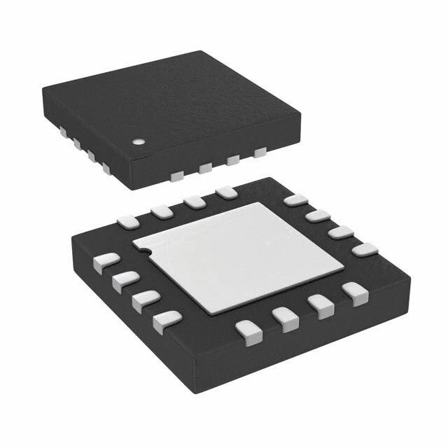
| 产品图片 |
|
| rohs | 符合RoHS无铅 / 符合限制有害物质指令(RoHS)规范要求 |
| 产品系列 | 逻辑集成电路,编码器、解码器、复用器和解复用器,Fairchild Semiconductor NC7SZ18P6X7SZ |
| 数据手册 | |
| 产品型号 | NC7SZ18P6X |
| PCN封装 | |
| PCN设计/规格 | |
| 产品 | Decoders, Encoders, Multiplexers & Demultiplexers |
| 产品种类 | 编码器、解码器、复用器和解复用器 |
| 供应商器件封装 | SC-70-6 |
| 其它名称 | NC7SZ18P6X-ND |
| 功率耗散 | 180 mW |
| 包装 | 带卷 (TR) |
| 单位重量 | 28 mg |
| 商标 | Fairchild Semiconductor |
| 安装类型 | 表面贴装 |
| 安装风格 | SMD/SMT |
| 封装 | Reel |
| 封装/外壳 | 6-TSSOP,SC-88,SOT-363 |
| 封装/箱体 | SC-70-6 |
| 工作温度 | -40°C ~ 85°C |
| 工厂包装数量 | 3000 |
| 最大工作温度 | + 85 C |
| 最小工作温度 | - 40 C |
| 标准包装 | 3,000 |
| 独立电路 | 1 |
| 电压-电源 | 1.65 V ~ 5.5 V |
| 电压源 | 单电源 |
| 电流-输出高,低 | 32mA,32mA |
| 电源电压-最大 | 5.5 V |
| 电源电压-最小 | 1.65 V |
| 电路 | 1 x 1:2 |
| 类型 | 多路分解器 |
| 系列 | NC7SZ18 |
| 输入/输出线数量 | 1 / 2 |
| 输入线路数量 | 1 |
| 输出线路数量 | 2 |
| 逻辑系列 | NC7 |
| 零件号别名 | NC7SZ18P6X_NL |


- 商务部:美国ITC正式对集成电路等产品启动337调查
- 曝三星4nm工艺存在良率问题 高通将骁龙8 Gen1或转产台积电
- 太阳诱电将投资9.5亿元在常州建新厂生产MLCC 预计2023年完工
- 英特尔发布欧洲新工厂建设计划 深化IDM 2.0 战略
- 台积电先进制程称霸业界 有大客户加持明年业绩稳了
- 达到5530亿美元!SIA预计今年全球半导体销售额将创下新高
- 英特尔拟将自动驾驶子公司Mobileye上市 估值或超500亿美元
- 三星加码芯片和SET,合并消费电子和移动部门,撤换高东真等 CEO
- 三星电子宣布重大人事变动 还合并消费电子和移动部门
- 海关总署:前11个月进口集成电路产品价值2.52万亿元 增长14.8%


PDF Datasheet 数据手册内容提取
N C 7 S Z June 2011 1 8 — T in y L NC7SZ18 o g TinyLogic® UHS 1-of-2 Non-Inverting De-multiplexer ic ® U with 3-STATE Deselected Output H S 1 - o f - 2 Features Description N o Ultra-High Speed: t 2.5ns Typical at 5V The NC7SZ18 is a 1-of-2 non-inverting demultiplexer. n PD VCC Teihthee dr eovuictpeu wt Yill bourf fYer dtheep ednadtae notn o nth ew hAe tphienr asntadt ep aosf st htoe -In High Impedance Output when Deselected select pin (S)0 is L1OW or HIGH respectively. The ve r Broad VCC Operating Range: 1.65V to 5.50V dsteasteel.e cTtheed oduetvpicuet wisil l fbaeb rpiclaatceedd winittoh aa dhvigahn cimedp eCdManOcSe tin Power Down High Impedance Inputs/Outputs technology to achieve ultra high speed with high output g D Over-Voltage Tolerance Inputs Facilitate 5V to 3V drive while maintaining low static power dissipation over e Translation a broad VCC operating range. The device is specified to -m operate over the 1.65V to 5.5V V operating range. Proprietary Noise/EMI Reduction Circuitry The inputs and outputs are high impCeCdance when VCC is ult Ultra-Small MicroPak™ Packages 0V. Inputs tolerate voltages up to 5.5V independent of ip VCC operating range. le x e r w it h Ordering Information 3 - S T Part Number Top Mark Package Packing Method A T NC7SZ18P6X Z18 6-Lead SC70, EIAJ SC88 1.25mm Wide 3000 Units on Tape & Reel E NC7SZ18L6X D5 6-Lead MicroPak™, 1.00mm Wide 5000 Units on Tape & Reel D e NC7SZ18FHX D5 6-Lead, MicroPak2™, 1x1mm Body, .35mm Pitch 5000 Units on Tape & Reel s e l e c t e d O u t p u t TinyLogic® is a registered trademark of Fairchild Semiconductor Corporation. MicroPak™ is a trademark of Fairchild Semiconductor Corporation. © 1999 Fairchild Semiconductor Corporation www.fairchildsemi.com NC7SZ18 • Rev. 1.0.2
N C Pin Configurations 7 S Z 1 8 — T i n y L o g i c ® U H S 1 -o f - 2 Figure 1. SC70 (Top View) Figure 2. MicroPak™ (Top Through View) N o n - I n v e r t i n g D e - m u Figure 3. Pin 1 Orientation l t i p Notes: l e 1. AAA represents product code top mark (see Ordering Information). x e 2. Orientation of top mark determines pin one location. r 3. Reading the top mark left to right, pin one is the lower left pin. w i Pin Definitions th 3 Pin # SC70 Pin # MicroPak™ Name Description - S 1 1 S Data Input T A 2 2 GND Ground T E 3 3 A Demultiplexer Data D 4 4 Y Output e 1 s 5 5 V Supply Voltage e CC l e 6 6 Y0 Output c t e d Function Table O u Inputs Output t p u S A Y Y 0 1 t L L L Z L H H Z H L Z L H H Z H H = HIGH Logic Level L = LOW Logic Level X = 3-STATE © 1999 Fairchild Semiconductor Corporation www.fairchildsemi.com NC7SZ18 • Rev. 1.0.2 2
N C Absolute Maximum Ratings 7 S Stresses exceeding the absolute maximum ratings may damage the device. The device may not function or be Z 1 operable above the recommended operating conditions and stressing the parts to these levels is not recommended. 8 In addition, extended exposure to stresses above the recommended operating conditions may affect device reliability. — The absolute maximum ratings are stress ratings only. T i Symbol Parameter Min. Max. Unit n y L VCC Supply Voltage -0.5 7.0 V o g VIN DC Input Voltage -0.5 7.0 V ic V DC Output Voltage -0.5 7.0 V ® OUT U I DC Input Diode Current V -0.5V -50 mA H IK IN S IOK DC Output Diode Current VIN -0.5V -50 mA 1 - I DC Output Current ±50 mA o OUT f - I or I DC V or Ground Current ±100 mA 2 CC GND CC N T Storage Temperature Range -65 +150 °C STG o T Junction Temperature Under Bias +150 °C n J - I T Junction Lead Temperature (Soldering, 10 Seconds) +260 °C n L v e SC70-6 180 r t i P Power Dissipation at +85°C MicroPak™-6 130 mW n D g MicroPak2™-6 120 D Human Body Model, JEDEC:JESD22-A114 4000 e - ESD V m Charge Device Model, JEDEC:JESD22-C101 2000 u l t i p Recommended Operating Conditions l e x The Recommended Operating Conditions table defines the conditions for actual device operation. Recommended e operating conditions are specified to ensure optimal performance to the datasheet specifications. Fairchild does not r w recommend exceeding them or designing to Absolute Maximum Ratings. i t h Symbol Parameter Conditions Min. Max. Unit 3 - S Supply Voltage Operating 1.65 5.50 T V V CC A Supply Voltage Data Retention 1.5 5.5 T V Input Voltage 0 5.5 V E IN D VOUT Output Voltage 0 VCC V e s V2.C5CV a ±t 10..82VV, ±0.15V, 0 20 ele t, t Input Rise and Fall Times ns/V c r f V at 3.3V ± 0.3V 0 10 t CC e d VCC at 5.0V ± 0.5V 0 5 O T Operating Temperature -40 +85 °C u A t p SC70-6 425 u t Thermal Resistance MicroPak™-6 500 °C/W JA MicroPak2™-6 560 © 1999 Fairchild Semiconductor Corporation www.fairchildsemi.com NC7SZ18 • Rev. 1.0.2 3
N C DC Electrical Characteristics 7 S Z T =+25°C TA=-40 to 1 A +85°C 8 Symbol Parameter V Condition Unit CC — Min. Typ. Max. Min. Max. T V HIGH Level Input 1.65 to 1.95 0.75VCC 0.75VCC V iny IH Voltage 2.30 to 5.50 0.70V 0.70V L CC CC o VIL LVOolWtag Lee vel Input 12..6350 ttoo 15..9550 00..2350VVCC 00..2350VVCC V gic® CC CC U 1.65 1.55 1.65 1.55 H 2.30 V =V , 2.20 2.30 2.20 S IN IH 1 3.00 IOH=-100µA 2.90 3.00 2.90 -o f 4.50 4.40 4.50 4.40 - 2 HIGH Level V 1.65 I =-4mA 1.29 1.52 1.29 V N OH Output Voltage OH o 2.30 IOH=-8mA 1.90 2.15 1.90 n - 3.00 IOH=-16mA 2.40 2.80 2.40 In v 3.00 I =-24mA 2.30 3.68 2.30 e OH r t 4.50 IOH=-32mA 3.80 4.20 3.80 in g 1.65 0.00 0.10 0.10 D 2.30 V =V 0.00 0.10 0.10 e IN IL - 3.00 IOL=100µA 0.00 0.10 0.10 m u 4.50 0.00 0.10 0.10 l t LOW Level ip V 1.65 I =4mA 0.08 0.24 0.24 V OL Output Voltage OL le 2.30 I =8mA 0.10 0.30 0.30 x OL e 3.00 IOL=16mA 0.15 0.40 0.40 r w 3.00 I =24mA 0.22 0.55 0.55 i OL t h 4.50 IOL=32mA 0.22 0.55 0.55 3 - Input Leakage S IIN Current 0 to 5.5 VIN=5.5V, GND ±0.1 ±1.0 µA T A 3-STATE Output V =V or V T I 1.65 to 5.50 IN IL OH ±0.5 ±5.0 µA E OZ Leakage 0<VOUT 5.5V D Power Off e I 0 V or V =5.5V 1 10 µA s OFF Leakage Current IN OUT e l Quiescent e I 1.65 to 5.50 V =5.5V, GND 1 10 µA c CC Supply Current IN t e d O u t p u t © 1999 Fairchild Semiconductor Corporation www.fairchildsemi.com NC7SZ18 • Rev. 1.0.2 4
N C AC Electrical Characteristics 7 S Z T =+25°C TA=-40 to 1 A +85°C 8 Symbol Parameter V Condition Unit Figure CC — Min. Typ. Max. Min. Max. T i 1.80 ± 0.15 2.0 6.3 10.1 2.0 10.5 n y 2.50 ± 0.20 CL=15pF, 1.0 3.6 5.7 1.0 6.0 L R =1M o 3.30 ± 0.30 D 0.8 2.7 4.0 0.8 4.3 g t , t Propagation Delay V1=OPEN ns Figure 4 ic PLH PHL A to Y or Y 5.00 ± 0.50 0.5 2.0 3.1 0.5 3.3 Figure 6 ® 0 1 U 3.30 ± 0.30 C =50pF, 1.2 3.4 4.9 1.2 5.4 L H RD=500 0.8 0.8 S 5.00 ± 0.50 V1=OPEN 2.5 3.9 4.2 1 - 1.80 ± 0.15 C =50pF, 3.0 6.9 12.0 3.0 12.5 o L f 2.50 ± 0.20 RD,RU=500 1.8 4.2 6.8 1.8 7.3 -2 Output Enable V1=GND for Figure 4 N 3.30 ± 0.30 t 1.2 3.2 5.0 1.2 5.5 ns o Time VPZ=H V for Figure 6 n 1 IN - 5.00 ± 0.50 tPZL 0.8 2.5 4.0 0.8 4.3 In V =2 x V v t , t IN CC e PZL PHZ r 1.80 ± 0.15 CL=50pF, 2.5 6.0 10.0 2.5 10.5 ti R R =500 n 2.50 ± 0.20 D, U 1.5 4.0 6.8 1.5 7.1 g Output Disable 3.30 ± 0.30 Vt 1=GND for 0.8 2.9 4.9 0.8 5.3 ns Figure 4 D Time PHZ Figure 6 e V =V for - 1 IN m 5.00 ± 0.50 tPLZ 0.3 1.8 3.5 0.3 3.7 u VIN=2 x VCC lt i C Input Capacitance 0 2.5 pF p IN l e Output x COUT Capacitance 0 4.0 pF er w CPD PCoawpaecr iDtainscseip(4a)t ion 35..3000 1196..50 pF Figure 5 ith 3 Note: - S 4. CPD is defined as the value of the internal equivalent capacitance which is derived from dynamic operating T current consumption (I ) at no output loading and operating at 50% duty cycle. C is related to I dynamic A CCD PD CCD T operating current by the expression: I =(C )(V )(f )+(I static). CCD PD CC IN CC E D e s e l e c t e d O u t p u t © 1999 Fairchild Semiconductor Corporation www.fairchildsemi.com NC7SZ18 • Rev. 1.0.2 5
N C 7 AC Loadings and Waveforms S Z 1 8 — T i n y L o g i c ® U H S 1 - o f -2 Notes: N 5. C includes load and stray capacitance. o L n 6. Input PRR = 1.0MHz, tW = 500ns. -I Figure 4. AC Test Circuit Figure 5. ICCD Test Circuit nv e r t i n g D e - m u l t i p l e x e r w i t h 3 - S T A T E Figure 6. AC Waveforms D e s e l e c t e d O u t p u t © 1999 Fairchild Semiconductor Corporation www.fairchildsemi.com NC7SZ18 • Rev. 1.0.2 6
N C Physical Dimensions 7 S Z 1 SYMM 8 CL — 2.00±0.20 A 0.65 T 0.50 MIN i n 6 4 B y L o g PIN ONE i 1.25±0.10 1.90 c ® U H 1 3 S 1 (0.25) 00..3105 0.40 MIN -o 0.65 0.10 A B 1.30 f-2 LAND PATTERN RECOMMENDATION N 1.30 o n - 10..0800 SEE DETAIL A In v e r t 1.10 i 0.80 n g 0.10 0.10 C D C 0.00 e 2.10±0.30 - SEATING m PLANE u l t i NOTES: UNLESS OTHERWISE SPECIFIED p l e GAGE A) THIS PACKAGE CONFORMS TO EIAJ x PLANE (R0.10) SC-88, 1996. e B) ALL DIMENSIONS ARE IN MILLIMETERS. r C) DIMENSIONS DO NOT INCLUDE BURRS w 0.25 0.10 OR MOLD FLASH. it 0.20 D) DRAWING FILENAME: MKT-MAA06AREV6 h 3 - 0.46 30° S 0.26 0° T A DETAIL A T SCALE: 60X E Figure 7. 6-Lead, SC70, EIAJ SC88, 1.25mm Wide D e s Package drawings are provided as a service to customers considering Fairchild components. Drawings may change in any manner e without notice. Please note the revision and/or date on the drawing and contact a Fairchild Semiconductor representative to verify or le obtain the most recent revision. Package specifications do not expand the terms of Fairchild’s worldwide terms and conditions, specifically the c t warranty therein, which covers Fairchild products. e d Always visit Fairchild Semiconductor’s online packaging area for the most recent package drawings: O http://www.fairchildsemi.com/packaging/. u tp u Tape and Reel Specification t Please visit Fairchild Semiconductor’s online packaging area for the most recent tape and reel specifications: http://www.fairchildsemi.com/products/analog/pdf/sc70-6_tr.pdf. Package Designator Tape Section Cavity Number Cavity Status Cover Type Status Leader (Start End) 125 (Typical) Empty Sealed P6X Carrier 3000 Filled Sealed Trailer (Hub End) 75 (Typical) Empty Sealed © 1999 Fairchild Semiconductor Corporation www.fairchildsemi.com NC7SZ18 • Rev. 1.0.2 7
N C 7 Physical Dimensions S Z 1 2X 8 0.05 C 1.45 B — 2X (1) T 0.05 C in y L o (0.254) 1.00 (0.49) gi 5X c ® (0.75) U H (0.52) S PIN 1 IDENTIFIER TOP VIEW A 1X 1 5 -o 0.55MAX (0.30) f - PIN 1 6X 2 0.05 C N 00..0050 RECOMMENED on LAND PATTERN - I 0.05 C n v C 0.45 e 0.25 6X 00..10006X 0.35 rtin 0.15 g DETAIL A 1.0 0.10 C B A D 0.05 C 0.40 e 0.30 - m u 00..3255 5X lti p l e 00..4300 5X DETAIL A xe 0.075 X 45 PIN 1 TERMINAL r w (0.05) 0.5 (0.13) CHAMFER it 6X h 4X BOTTOM VIEW 3 Notes: - S 1. CONFORMS TO JEDEC STANDARD M0-252 VARIATION UAAD T 2. DIMENSIONS ARE IN MILLIMETERS A 3. DRAWING CONFORMS TO ASME Y14.5M-1994 T E 4. FILENAME AND REVISION: MAC06AREV4 5. PIN ONE IDENTIFIER IS 2X LENGTH OF ANY D e OTHER LINE IN THE MARK CODE LAYOUT. s e Figure 8. 6-Lead, MicroPak™, 1.0mm Wide l e c Package drawings are provided as a service to customers considering Fairchild components. Drawings may change in any manner t without notice. Please note the revision and/or date on the drawing and contact a Fairchild Semiconductor representative to verify or e d obtain the most recent revision. Package specifications do not expand the terms of Fairchild’s worldwide terms and conditions, specifically the O warranty therein, which covers Fairchild products. u t Always visit Fairchild Semiconductor’s online packaging area for the most recent package drawings: p http://www.fairchildsemi.com/packaging/. u t Tape and Reel Specification Please visit Fairchild Semiconductor’s online packaging area for the most recent tape and reel specifications: http://www.fairchildsemi.com/products/logic/pdf/micropak_tr.pdf. Package Designator Tape Section Cavity Number Cavity Status Cover Type Status Leader (Start End) 125 (Typical) Empty Sealed L6X Carrier 5000 Filled Sealed Trailer (Hub End) 75 (Typical) Empty Sealed © 1999 Fairchild Semiconductor Corporation www.fairchildsemi.com NC7SZ18 • Rev. 1.0.2 8
N C 7 Physical Dimensions S Z 1 0.89 8 — 0.05 C 0.35 2X 1.00 B A T 5X 0.40 in y L PIN 1 o 0.66 MIN 250uM g 1.00 ic 1X 0.45 ® U H 6X 0.19 S 0.05 C TOP VIEW 2X RECOMMENDED LAND PATTERN 1 - FOR SPACE CONSTRAINED PCB o f 0.90 - 2 0.05 C 0.35 N o n C 0.55MAX 5X0.52 -I n v e SIDE VIEW 0.73 r t i n (0.08) 4X 0.09 1X0.57 g DETAIL A 1 2 3 0.19 6X D e - 0.20 6X m u ALTERNATIVE LAND PATTERN l t FOR UNIVERSAL APPLICATION i p l (0.05) 6X e x e 5X0.35 r 0.25 0.60 w 0.35 6 5 4 (0.08) .00.510C C B A 0.40 ith 4X 0.30 3 BOTTOM VIEW - S NOTES: T A. COMPLIES TO JEDEC MO-252 STANDARD A B. DIMENSIONS ARE IN MILLIMETERS. T C. DIMENSIONS AND TOLERANCES PER ASME Y14.5M, 1994 0.075X45° E D. LANDPATTERN RECOMMENDATION IS BASED ON FSC CHAMFER DETAIL A DESIGN. PIN 1 LEAD SCALE: 2X D E. DRAWING FILENAME AND REVISION: MGF06AREV3 es Figure 9. 6-Lead, MicroPak2™, 1x1mm Body, .35mm Pitch e l e Package drawings are provided as a service to customers considering Fairchild components. Drawings may change in any manner c without notice. Please note the revision and/or date on the drawing and contact a Fairchild Semiconductor representative to verify or te obtain the most recent revision. Package specifications do not expand the terms of Fairchild’s worldwide terms and conditions, specifically the d warranty therein, which covers Fairchild products. O u Always visit Fairchild Semiconductor’s online packaging area for the most recent package drawings: tp http://www.fairchildsemi.com/packaging/. u t Tape and Reel Specification Please visit Fairchild Semiconductor’s online packaging area for the most recent tape and reel specifications: http://www.fairchildsemi.com/packaging/MicroPAK2_6L_tr.pdf. Package Designator Tape Section Cavity Number Cavity Status Cover Type Status Leader (Start End) 125 (Typical) Empty Sealed FHX Carrier 5000 Filled Sealed Trailer (Hub End) 75 (Typical) Empty Sealed © 1999 Fairchild Semiconductor Corporation www.fairchildsemi.com NC7SZ18 • Rev. 1.0.2 9
N C 7 S Z 1 8 — T i n y L o g i c ® U H S 1 - o f - 2 N o n - I n v e r t i n g D e - m u l t i p l e x e r w i t h 3 - S T A T E D e s e l e c t e d O u t p u t © 1999 Fairchild Semiconductor Corporation www.fairchildsemi.com NC7SZ18 • Rev. 1.0.2 10
Mouser Electronics Authorized Distributor Click to View Pricing, Inventory, Delivery & Lifecycle Information: O N Semiconductor: NC7SZ18L6X NC7SZ18P6X NC7SZ18FHX