ICGOO在线商城 > 集成电路(IC) > 逻辑 - 栅极和逆变器 - 多功能,可配置 > NC7SV58P6X
 Datasheet下载
- 型号: NC7SV58P6X
- 制造商: Fairchild Semiconductor
- 库位|库存: xxxx|xxxx
- 要求:
| 数量阶梯 | 香港交货 | 国内含税 |
| +xxxx | $xxxx | ¥xxxx |
查看当月历史价格
查看今年历史价格
NC7SV58P6X产品简介:
ICGOO电子元器件商城为您提供NC7SV58P6X由Fairchild Semiconductor设计生产,在icgoo商城现货销售,并且可以通过原厂、代理商等渠道进行代购。 NC7SV58P6X价格参考。Fairchild SemiconductorNC7SV58P6X封装/规格:逻辑 - 栅极和逆变器 - 多功能,可配置, Configurable Multiple Function Configurable 1 Circuit 3 Input SC-70-6。您可以下载NC7SV58P6X参考资料、Datasheet数据手册功能说明书,资料中有NC7SV58P6X 详细功能的应用电路图电压和使用方法及教程。
ON Semiconductor的NC7SV58P6X是一款单栅极、低功耗、高速的多功能可配置逻辑器件,属于微型逻辑IC系列,常用于需要灵活逻辑功能配置的数字电路设计中。

 主要应用场景包括:

1. 逻辑功能定制:
   NC7SV58P6X可通过输入端配置为实现多种逻辑功能(如AND、OR、NAND、NOR、XOR、XNOR等),适用于需要灵活实现不同逻辑功能的小型数字系统。

2. 信号处理与转换:
   广泛应用于数字信号路径中的逻辑转换、电平转换和信号处理,尤其适合空间受限的便携设备和通信设备。

3. 便携式电子产品:
   因其低功耗和小封装(如SC-70或TDFN),常用于手机、平板、可穿戴设备等对功耗和尺寸要求严格的场景。

4. 工业控制与接口电路:
   在PLC、传感器接口、继电器控制等工业应用中,用于实现逻辑控制和信号调节。

5. 测试与测量设备:
   用于逻辑分析仪、示波器等测试设备中,实现灵活的信号处理和逻辑判断。

6. 汽车电子:
   适用于车载控制系统、车身电子模块等对可靠性要求较高的汽车应用。

总结来说,NC7SV58P6X适用于需要多功能、低功耗、高集成度逻辑解决方案的多种电子系统中。
| 参数 | 数值 |
| 产品目录 | 集成电路 (IC)半导体 |
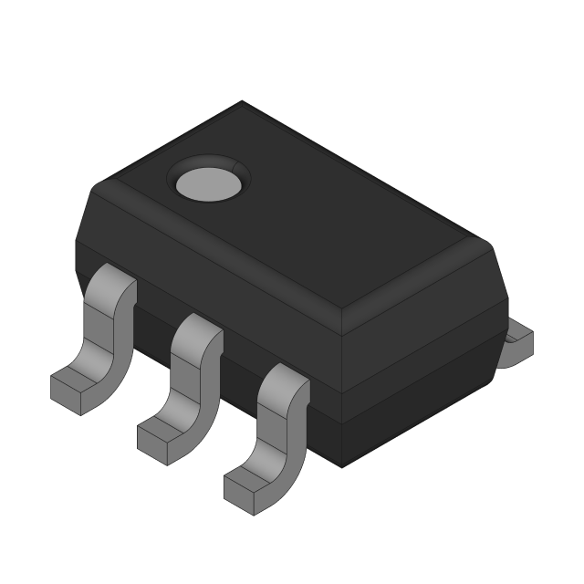
| 描述 | IC CONFIG MULT FUNCTION SC70-6逻辑门 2-Input Logic Gate |
| 产品分类 | |
| 品牌 | Fairchild Semiconductor |
| 产品手册 | |
| 产品图片 |
|
| rohs | 符合RoHS无铅 / 符合限制有害物质指令(RoHS)规范要求 |
| 产品系列 | 逻辑集成电路,逻辑门,Fairchild Semiconductor NC7SV58P6X7SV |
| 数据手册 | |
| 产品型号 | NC7SV58P6X |
| PCN封装 | |
| PCN设计/规格 | |
| 产品 | MUX Gates |
| 产品种类 | 逻辑门 |
| 传播延迟时间 | 9.1 ns |
| 低电平输出电流 | 24 mA |
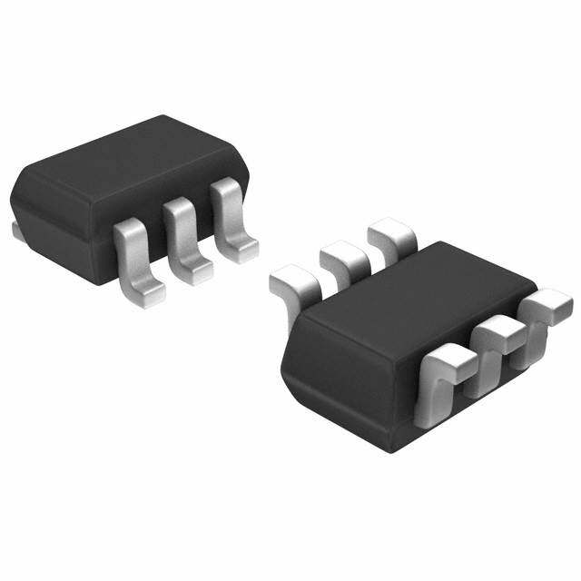
| 供应商器件封装 | SC-70-6 |
| 其它名称 | NC7SV58P6XCT |
| 包装 | 剪切带 (CT) |
| 单位重量 | 28 mg |
| 商标 | Fairchild Semiconductor |
| 安装类型 | 表面贴装 |
| 安装风格 | SMD/SMT |
| 封装 | Reel |
| 封装/外壳 | 6-TSSOP,SC-88,SOT-363 |
| 封装/箱体 | SC-70 |
| 工作温度 | -40°C ~ 85°C |
| 工厂包装数量 | 3000 |
| 施密特触发器输入 | 是 |
| 最大工作温度 | + 85 C |
| 最小工作温度 | - 40 C |
| 栅极数量 | 1 Gate |
| 标准包装 | 1 |
| 电压-电源 | 0.9 V ~ 3.6 V |
| 电流-输出高,低 | 24mA,24mA |
| 电源电压-最大 | 3.6 V |
| 电源电压-最小 | 0.9 V |
| 电路数 | 1 |
| 系列 | NC7SV58 |
| 输入/输出线数量 | 2 / 1 |
| 输入数 | 2 |
| 输入线路数量 | 2 |
| 输出类型 | 单端 |
| 输出线路数量 | 1 |
| 逻辑类型 | 可配置多功能 |
| 逻辑系列 | NC7SV |
| 高电平输出电流 | - 24 mA |


- 商务部:美国ITC正式对集成电路等产品启动337调查
- 曝三星4nm工艺存在良率问题 高通将骁龙8 Gen1或转产台积电
- 太阳诱电将投资9.5亿元在常州建新厂生产MLCC 预计2023年完工
- 英特尔发布欧洲新工厂建设计划 深化IDM 2.0 战略
- 台积电先进制程称霸业界 有大客户加持明年业绩稳了
- 达到5530亿美元!SIA预计今年全球半导体销售额将创下新高
- 英特尔拟将自动驾驶子公司Mobileye上市 估值或超500亿美元
- 三星加码芯片和SET,合并消费电子和移动部门,撤换高东真等 CEO
- 三星电子宣布重大人事变动 还合并消费电子和移动部门
- 海关总署:前11个月进口集成电路产品价值2.52万亿元 增长14.8%


PDF Datasheet 数据手册内容提取
Is Now Part of To learn more about ON Semiconductor, please visit our website at www.onsemi.com Please note: As part of the Fairchild Semiconductor integration, some of the Fairchild orderable part numbers will need to change in order to meet ON Semiconductor’s system requirements. Since the ON Semiconductor product management systems do not have the ability to manage part nomenclature that utilizes an underscore (_), the underscore (_) in the Fairchild part numbers will be changed to a dash (-). This document may contain device numbers with an underscore (_). Please check the ON Semiconductor website to verify the updated device numbers. The most current and up-to-date ordering information can be found at www.onsemi.com. Please email any questions regarding the system integration to Fairchild_questions@onsemi.com. ON Semiconductor and the ON Semiconductor logo are trademarks of Semiconductor Components Industries, LLC dba ON Semiconductor or its subsidiaries in the United States and/or other countries. ON Semiconductor owns the rights to a number of patents, trademarks, copyrights, trade secrets, and other intellectual property. A listing of ON Semiconductor’s product/patent coverage may be accessed at www.onsemi.com/site/pdf/Patent-Marking.pdf. ON Semiconductor reserves the right to make changes without further notice to any products herein. ON Semiconductor makes no warranty, representation or guarantee regarding the suitability of its products for any particular purpose, nor does ON Semiconductor assume any liability arising out of the application or use of any product or circuit, and specifically disclaims any and all liability, including without limitation special, consequential or incidental damages. Buyer is responsible for its products and applications using ON Semiconductor products, including compliance with all laws, regulations and safety requirements or standards, regardless of any support or applications information provided by ON Semiconductor. “Typical” parameters which may be provided in ON Semiconductor data sheets and/or specifications can and do vary in different applications and actual performance may vary over time. All operating parameters, including “Typicals” must be validated for each customer application by customer’s technical experts. ON Semiconductor does not convey any license under its patent rights nor the rights of others. ON Semiconductor products are not designed, intended, or authorized for use as a critical component in life support systems or any FDA Class 3 medical devices or medical devices with a same or similar classification in a foreign jurisdiction or any devices intended for implantation in the human body. Should Buyer purchase or use ON Semiconductor products for any such unintended or unauthorized application, Buyer shall indemnify and hold ON Semiconductor and its officers, employees, subsidiaries, affiliates, and distributors harmless against all claims, costs, damages, and expenses, and reasonable attorney fees arising out of, directly or indirectly, any claim of personal injury or death associated with such unintended or unauthorized use, even if such claim alleges that ON Semiconductor was negligent regarding the design or manufacture of the part. ON Semiconductor is an Equal Opportunity/Affirmative Action Employer. This literature is subject to all applicable copyright laws and is not for resale in any manner.
N C 7 S V December 2010 5 7 / N C NC7SV57 / NC7SV58 7 S ® V TinyLogic ULP-A Universal Configurable Two-Input 5 8 Logic Gates — T i n Features Description y L o (cid:131) 0.9V to 3.6V VCC Supply Operation The NC7SV57 and NC7SV58 are universal configurable g two-input logic gates from Fairchild’s Ultra-Low Power i (cid:131) 3.6V Over-Voltage Tolerant I/Os at VCC (ULP-A) series of TinyLogic®. ULP-A is ideal for c® from 0.9V to 3.6V applications that require extreme high-speed, high U (cid:131) Extremely High Speed tPD drive, and low power. This product is designed for a LP - 2.5ns: Typical for 2.7V to 3.6V VCC wide low-voltage operating range (0.9V to 3.6V VCC) -A and applications that require more drive and speed than - 3.1ns: Typical for 2.3V to 2.7V VCC the TinyLogic® ULP series, but still offer best-in-class, U - 4.0ns: Typical for 1.65V to 1.95V VCC low-power operation. n i - 6.0ns: Typical for 1.4V to 1.6V VCC Each device is capable of being configured for 1 of 5 ve - 8.0ns: Typical for 1.1V to 1.3V VCC unique two-input logic functions. Any possible two-input rs - 23.0ns: Typical for 0.9V VCC combinatorial logic function can be implemented, as al (cid:131) Power-Off High-Impedance Inputs and Outputs shown in the Function Selection Table. Device C functionality is selected by how the device is wired at o (cid:131) High Static Drive (I /I ) n OH OL the board level. Figures 1 through 10 illustrate how to f - ±24mA at 3.00V VCC connect the NC7SV57 and NC7SV58, respectively, for ig u - ±18mA at 2.30V VCC the desired logic function. All inputs have been r implemented with hysteresis. a - ±6mA at 1.65V VCC ti o - ±4mA at 1.4V VCC The NC7SV57 and NC7SV58 are uniquely designed for n optimized power and speed and are fabricated with an - ±2mA at 1.1V VCC T advanced CMOS technology to achieve high-speed w - ±0.1mA at 0.9V VCC operation while maintaining low CMOS power o (cid:131) Proprietary Quiet Series™ Noise/EMI Reduction dissipation. -I n (cid:131) Ultra-Small MicroPak™ Package pu (cid:131) Ultra-Low Dynamic Power t L o g Ordering Information ic G Part Number Top Mark Package Packing Method a t e s 3000 Units on NC7SV57P6X V57 6-Lead SC70, EIAJ SC-88a, 1.25mm Wide Tape & Reel NC7SV57L6X H3 6-Lead Micropak™, 1.0mm Wide 5000 Units on NC7SV57FHX H3 6-Lead, MicroPak2™, 1x1mm Body, .35mm Pitch Tape & Reel 3000 Units on NC7SV58P6X V58 6-Lead SC70, EIAJ SC-88a, 1.25mm Wide Tape & Reel NC7SV58L6X H4 6-Lead Micropak™, 1.0mm Wide 5000 Units on NC7SV58FHX H4 6-Lead, MicroPak2™, 1x1mm Body, .35mm Pitch Tape & Reel © 2002 Fairchild Semiconductor Corporation www.fairchildsemi.com NC7SV57 • NC7SV58 • Rev. 1.0.4
N C Battery Life 7 S V 5 7 / N C 7 V 5 8 — T i n y L o g i c ® Figure 1. Battery Life vs. VCC Supply Voltage U L Notes: P 1. TinyLogic® ULP and ULP-A with up to 50% less power consumption can extend your battery life significantly. A Battery Life = (Vbattery•Ibattery•.9)/(Pdevice)/24hrs/day U where P = (I • V ) + (C + C ) • V 2• f. n device CC CC PD L CC i 2. Assumes ideal 3.6V Lithium Ion battery with current rating of 900mAH and derated 90% and device frequency at v e 10MHz, with CL = 15pF load. r s a l C o n f i g u r a t i o n T w o - I n p u t L o g i c G a t e s © 2002 Fairchild Semiconductor Corporation www.fairchildsemi.com NC7SV57 • NC7SV58 • Rev. 1.0.4 2
N C Pin Configurations 7 S V 5 7 / N C 7 V 5 8 — T i n y L o Figure 2. SC70 (Top View) Figure 3. MicroPak™ (Top Through View) g i c ® U L P A U n i v e r s a l Figure 4. Pin 1 Orientation C o n Notes: f i 3. AAA represents product code top mark (see Ordering Information). g u 4. Orientation of top mark determines pin one location. r 5. Reading the top mark left to right, pin one is the lower left pin. a t i o n T w o - I n p u Pin Definitions t L o Pin # SC70 Pin # MicroPak™ Name Description g i c 1 1 I1 Data Input G 2 2 GND Ground a t e 3 3 I0 Data Input s 4 4 Y Output 5 5 V Supply Voltage CC 6 6 I Data Input 2 © 2002 Fairchild Semiconductor Corporation www.fairchildsemi.com NC7SV57 • NC7SV58 • Rev. 1.0.4 3
N C Function Table 7 S V Inputs NC7SV57 NC7SV58 5 7 I2 I1 I0 Y = (I0) • (I2) + (I1) • (I2) Y = (I0) • (I2) + (I1) • (I2) / N L L L H L C 7 L L H L H V 5 L H L H L 8 — L H H L H T H L L L H i n H L H L H y L H H L H L o g H H H H L ic ® U H = HIGH Logic Level L L = LOW Logic Level P A U n i Function Selection Table v e r s 2-Input Logic Function Device Selection Connection Configuration a l 2-Input AND NC7SV57 Figure 5 C o 2-Input AND with Inverted Input NC7SV58 Figure 11, Figure 12 n f i 2-Input AND with Both Inputs Inverted NC7SV57 Figure 8 g u 2-Input NAND NC7SV58 Figure 10 ra t 2-Input NAND with Inverted Input NC7SV57 Figure 6, Figure 7 io n 2-Input NAND with Both Inputs Inverted NC7SV58 Figure 13 T 2-Input OR NC7SV58 Figure 13 w o 2-Input OR with Inverted Input NC7SV57 Figure 6, Figure 7 - I n 2-Input OR with Both Inputs Inverted NC7SV58 Figure 10 p u 2-Input NOR NC7SV57 Figure 8 t L 2-Input NOR with Inverted Input NC7SV58 Figure 10, Figure 11 o g 2-Input NOR with Both Inputs Inverted NC7SV57 Figure 5 ic 2-Input XOR NC7SV58 Figure 14 G a 2-Input XNOR NC7SV57 Figure 9 t e s © 2002 Fairchild Semiconductor Corporation www.fairchildsemi.com NC7SV57 • NC7SV58 • Rev. 1.0.4 4
N C NC7SV57 Logic Configurations 7 S Figure 5 through Figure 9 show the logical functions implementation is next to the board-level physical V that can be implemented using the NC7SV57. The implementation of how the pins of the function should 5 7 diagrams show the DeMorgan’s equivalent logic duals be connected. / for a given two-input function. The logical N C 7 V 5 8 — T i n y L o g ic ® Figure 5. 2-Input AND Gate Figure 6. 2-Input NAND Gate with Inverted A Input U L P A U n i v e r s a l C o n fi g Figure 7. 2-Input NAND with Inverted B Input Figure 8. 2-Input NOR Gate u r a t i o n T w o - I n p u t L o g i Figure 9. 2-Input XNOR Gate c G a t e s © 2002 Fairchild Semiconductor Corporation www.fairchildsemi.com NC7SV57 • NC7SV58 • Rev. 1.0.4 5
N C NC7SV58 Logic Configurations 7 S Figure 10 through Figure 14 show the logical functions implementation is next to the board-level physical V that can be implemented using the NC7SV58. The implementation of how the pins of the function should 5 7 diagrams show the DeMorgan’s equivalent logic duals be connected. / for a given two-input function. The logical N C 7 V 5 8 — T i n y L o g i c Figure 10. 2-Input NAND Gate Figure 11. 2-Input AND Gate with Inverted A Input ® U L P A U n i v e r s a l C o n f Figure 12. 2-Input AND with Inverted B Input Figure 13. 2-Input OR Gate ig u r a t i o n T w o - I n p u t L o g Figure 14. 2-Input XOR Gate i c G a t e s © 2002 Fairchild Semiconductor Corporation www.fairchildsemi.com NC7SV57 • NC7SV58 • Rev. 1.0.4 6
N C Absolute Maximum Ratings 7 S Stresses exceeding the absolute maximum ratings may damage the device. The device may not function or be V operable above the recommended operating conditions and stressing the parts to these levels is not recommended. 5 7 In addition, extended exposure to stresses above the recommended operating conditions may affect device / reliability. The absolute maximum ratings are stress ratings only. N C Symbol Parameter Min. Max. Unit 7 V 5 VCC Supply Voltage -0.5 4.6 V 8 V DC Input Voltage -0.5 4.6 V — IN HIGH or LOW State(6) -0.5 V + 0.5 T VOUT DC Output Voltage CC V in VCC=0V -0.5 4.6 y L IIK DC Input Diode Current VIN < 0V ±50 mA o g VOUT < 0V -50 ic I DC Output Diode Current mA OK ® VOUT > VCC +50 U I / I DC Output Source / Sink Current ±50 mA L OH OL P ICC or IGND DC VCC or Ground Current per Supply Pin ±50 mA A T Storage Temperature Range -65 +150 °C U STG n MicroPak™-6 130 i v e P Power Dissipation at +85°C SC70-6 150 mW D r s MicroPak2™-6 120 a l Human Body Model, JEDEC:JESD22-A114 4000 C ESD V o Charged Device Model, JEDEC:JESD22-C101 2000 n f i Note: g u 6. IO absolute maximum rating must be observed. r a t i Recommended Operating Conditions o n The Recommended Operating Conditions table defines the conditions for actual device operation. Recommended T w operating conditions are specified to ensure optimal performance to the datasheet specifications. Fairchild does not o recommend exceeding them or designing to Absolute Maximum Ratings. - I n p Symbol Parameter Conditions Min. Max. Unit u t VCC Supply Voltage Operating 0.9 3.6 V L o VIN Input Voltage 0 3.6 V g i V =0V 0 3.6 c CC V Output Voltage V G OUT HIGH or LOW State 0 VCC a t V =3.0V to 3.6V ±24.0 e CC s V =2.3V to 2.7V ±18.0 CC V =1.65V to 1.95V ±6.0 mA CC I /I Output Current OH OL V =1.4V to 1.6V ±4.0 CC V =1.1V to 1.3V ±2.0 CC V =0.9V ±0.1 µA CC T Operating Temperature, Free Air -40 +85 °C A Δt/ΔV Minimum Input Edge Rate VIN=0.8V to 2.0, VCC=3.0V 10 ns/V SC70-6 425 θ Thermal Resistance MicroPak™-6 500 °C/W JA MicroPak2™-6 560 Note: 7. Unused inputs must be held HIGH or LOW. They may not float. © 2002 Fairchild Semiconductor Corporation www.fairchildsemi.com NC7SV57 • NC7SV58 • Rev. 1.0.4 7
N C DC Electrical Characteristics 7 S V T =25°C T =-40 to 85°C Symbol Parameter V Conditions A A Units 5 CC 7 Min. Max. Min. Max. / 0.90 0.30 0.70 0.30 0.70 N C 1.10 0.40 1.00 0.40 1.00 7 V Positive Threshold 1.40 0.50 1.40 0.50 1.40 5 VP Voltage 1.65 0.70 1.50 0.70 1.50 V 8 — 2.30 1.00 1.80 1.00 1.80 T 2.70 1.30 2.20 1.30 2.20 i n 0.90 0.10 0.60 0.10 0.60 y L 1.10 0.15 0.70 0.15 0.70 o g Negative Threshold 1.40 0.20 0.80 0.20 0.80 ic VN Voltage 1.65 0.25 0.90 0.25 0.90 V ® U 2.30 0.40 1.15 0.40 1.15 L P 2.70 0.60 1.50 0.60 1.50 A 0.90 0.07 0.50 0.07 0.50 U n 1.10 0.08 0.60 0.08 0.60 i v 1.40 0.10 0.80 0.10 0.80 e VH Hysteresis Voltage 1.65 0.15 1.00 0.15 1.00 V rs a 2.30 0.25 1.10 0.25 1.10 l C 2.70 0.40 1.20 0.40 1.20 o n 0.90 VCC-0.1 VCC-0.1 fi g 1.10 ≤ VCC ≤ 1.30 VCC-0.1 VCC-0.1 u r 11.6.450 ≤ ≤ V VCCCC ≤≤ 11..9650 IOH=-100µA VVCCCC--00..22 VVCCCC--00..22 ation 2.30 ≤ VCC ≤ 2.70 VCC-0.2 VCC-0.2 T w 2.70 ≤ VCC ≤ 3.60 VCC-0.2 VCC-0.2 o - 1.10 ≤ VCC ≤ 1.30 IOH=-2mA .75 x VCC .75 x VCC In HIGH Level Output p VOH Voltage 1.40 ≤ VCC ≤ 1.60 IOH=-4mA .75 x VCC .75 x VCC V u 12..6350 ≤≤ VVCCCC ≤≤ 12..9750 IOH=-6mA 12..205 12..205 t Log 2.30 ≤ VCC ≤ 2.70 1.8 1.8 ic IOH=-12mA G 2.70 ≤ VCC ≤ 3.60 2.2 2.2 a 2.30 ≤ VCC ≤ 2.70 1.7 1.7 te IOH=-18mA s 2.70 ≤ VCC ≤ 3.60 2.4 2.4 2.70 ≤ VCC ≤ 3.60 IOH=-24mA 2.2 2.2 Continued on following page…. © 2002 Fairchild Semiconductor Corporation www.fairchildsemi.com NC7SV57 • NC7SV58 • Rev. 1.0.4 8
N C DC Electrical Characteristics (Continued) 7 S V T =25°C T =-40 to 85°C A A 5 Symbol Parameter VCC Conditions Units 7 Min. Max. Min. Max. / N 0.90 0.1 0.1 C 1.10 ≤ VCC ≤ 1.30 0.1 0.1 7V 1.40 ≤ VCC ≤ 1.60 0.2 0.2 58 IOL=100µA 1.65 ≤ VCC ≤ 1.95 0.2 0.2 — 2.30 ≤ VCC ≤ 2.70 0.2 0.2 T i 2.70 ≤ VCC ≤ 3.60 0.2 0.2 ny L LOW Level Output 1.10 ≤ VCC ≤ 1.30 IOL=2mA .25 x VCC .25 x VCC o VOL Voltage 1.40 ≤ VCC ≤ 1.60 IOL=4mA .25 x VCC .25 x VCC V gi c 1.65 ≤ VCC ≤ 1.95 IOL=6mA 0.3 0.3 ® U 2.30 ≤ VCC ≤ 2.70 0.4 0.4 L IOL=12mA P 2.70 ≤ VCC ≤ 3.60 0.4 0.4 A 2.30 ≤ VCC ≤ 2.70 IOL=18mA 0.6 0.6 U 2.70 ≤ VCC ≤ 3.60 0.4 0.4 n i v 2.70 ≤ VCC ≤ 3.60 IOL=24mA 0.55 0.55 e r Input Leakage s IIN Current 0.90 to 3.60 0 ≤ VIN ≤ 3.6V ±0.1 ±0.5 µA a l Power Off Leakage C IOFF Current 0 0 ≤ (VIN, VO) ≤ 3.60 0.5 0.5 µA o n ICC QCuurieresncte nt Supply 0.90 to 3.60 VVICNC= V≤ CVCI No ≤r G3.N6DV 0. 9 ±00.9.9 µA figur a t i o n AC Electrical Characteristics T w o T =25°C T =-40 to 85°C A A - Symbol Parameter VCC Conditions Units Figure In Min. Typ. Min. Typ. Min. p u 0.90 CRLL==11M5pΩF , 15.0 t Lo tPHL, tPLH PDreolapya gation 11..1400 ≤≤ VVCCCC ≤≤ 11..3600 CL=15pF, RL=2KΩ 24..00 86..00 1106..05 23..03 1321..00 ns FFiigguurree 1165 gic G 1.65 ≤ VCC ≤ 1.95 2.0 4.0 9.1 1.9 10.0 a 2.30 ≤ VCC ≤ 2.70 CRLL==53000pΩF, 1.5 3.1 6.2 1.4 6.7 tes 2.70 ≤ VCC ≤ 3.60 1.2 2.5 5.4 1.2 6.1 Input CIN Capacitance 0 8 pF Output COUT Capacitance 0 12 pF Power CPD Dissipation 0.90 to 3.60 Vf=I=100MV Horz VCC, 10 pF Capacitance © 2002 Fairchild Semiconductor Corporation www.fairchildsemi.com NC7SV57 • NC7SV58 • Rev. 1.0.4 9
N C AC Loadings and Waveforms 7 S V 5 7 / N C 7 V 5 8 — T i n y L o g Figure 15. AC Test Circuit ic ® U L P A U n i v e r s a l C o n f i g u r a Figure 16. AC Waveforms t i o n T w V CC o Symbol - 3.3V ± 0.3V 2.5V ± 0.2V 1.8V ± 0.15V 1.5V ± 0.10V 1.2V ± 0.10V 0.9V In p V 1.5V V /2 V /2 V /2 V /2 V /2 u mi CC CC CC CC CC t V 1.5V V /2 V /2 V /2 V /2 V /2 L mo CC CC CC CC CC o g i c G a t e s © 2002 Fairchild Semiconductor Corporation www.fairchildsemi.com NC7SV57 • NC7SV58 • Rev. 1.0.4 10
N C Physical Dimensions 7 S SYMM V CL 5 7 2.00±0.20 A 0.65 / 0.50 MIN N C 6 4 B 7 V 5 8 PIN ONE 1.25±0.10 1.90 — T i n 1 3 y L (0.25) 00..3105 0.40 MIN og i 0.10 A B 1.30 c 0.65 ® U LAND PATTERN RECOMMENDATION 1.30 L P A 1.00 SEE DETAIL A 0.80 U n i v 1.10 e 0.80 r s a 0.10 0.10 C l C 0.00 C 2.10±0.30 o SEATING n PLANE f i g u NOTES: UNLESS OTHERWISE SPECIFIED r a GAGE A) THIS PACKAGE CONFORMS TO EIAJ ti PLANE (R0.10) SC-88, 1996. on B) ALL DIMENSIONS ARE IN MILLIMETERS. C) DIMENSIONS DO NOT INCLUDE BURRS T 00..2150 OR MOLD FLASH. w 0.20 D) DRAWING FILENAME: MKT-MAA06AREV6 o - I n 0.46 30° p 0.26 0° u t L DETAIL A SCALE: 60X o g Figure 17. 6-Lead, SC70, EIAJ SC-88a, 1.25mm Wide i c Package drawings are provided as a service to customers considering Fairchild components. Drawings may change in any manner G without notice. Please note the revision and/or date on the drawing and contact a Fairchild Semiconductor representative to verify a or obtain the most recent revision. Package specifications do not expand the terms of Fairchild’s worldwide terms and conditions, specifically te the warranty therein, which covers Fairchild products. s Always visit Fairchild Semiconductor’s online packaging area for the most recent package drawings: http://www.fairchildsemi.com/packaging/. Tape and Reel Specifications Please visit Fairchild Semiconductor’s online packaging area for the most recent tape and reel specifications: http://www.fairchildsemi.com/products/analog/pdf/sc70-6_tr.pdf Package Designator Tape Section Cavity Number Cavity Status Cover Type Status Leader (Start End) 125 (Typical) Empty Sealed P6X Carrier 3000 Filled Sealed Trailer (Hub End) 75 (Typical) Empty Sealed © 2002 Fairchild Semiconductor Corporation www.fairchildsemi.com NC7SV57 • NC7SV58 • Rev. 1.0.4 11
N C 7 Physical Dimensions S V 5 2X 7 0.05 C 1.45 B / 2X (1) N C 0.05 C 7 V 5 8 (0.254) 1.00 (0.49) — 5X (0.75) T i n y (0.52) L PIN 1 IDENTIFIER TOP VIEW A 1X o g 5 i 0.55MAX (0.30) c ® PIN 1 6X U 0.05 C L 0.05 RECOMMENED P 0.00 LAND PATTERN A 0.05 C U C n 0.25 00..10006X 00..4355 ive 6X r 0.15 s DETAIL A 1.0 a 0.10 C B A l 0.05 C 0.40 C 0.30 o n f 0.35 5X ig 0.25 u r a t 00..4300 5X 0.075 X 45 DPIENT 1A ITLE ARMINAL ion (0.05) 0.5 (0.13) CHAMFER Tw 6X 4X o BOTTOM VIEW - I Notes: n p 1. CONFORMS TO JEDEC STANDARD M0-252 VARIATION UAAD u 2. DIMENSIONS ARE IN MILLIMETERS t 3. DRAWING CONFORMS TO ASME Y14.5M-1994 L o 4. FILENAME AND REVISION: MAC06AREV4 g 5. PIN ONE IDENTIFIER IS 2X LENGTH OF ANY i c OTHER LINE IN THE MARK CODE LAYOUT. G Figure 18. 6-Lead, MicroPak™, 1.0mm Wide a t e Package drawings are provided as a service to customers considering Fairchild components. Drawings may change in any manner s without notice. Please note the revision and/or date on the drawing and contact a Fairchild Semiconductor representative to verify or obtain the most recent revision. Package specifications do not expand the terms of Fairchild’s worldwide terms and conditions, specifically the warranty therein, which covers Fairchild products. Always visit Fairchild Semiconductor’s online packaging area for the most recent package drawings: http://www.fairchildsemi.com/packaging/. Tape and Reel Specifications Please visit Fairchild Semiconductor’s online packaging area for the most recent tape and reel specifications: http://www.fairchildsemi.com/products/logic/pdf/micropak_tr.pdf. Package Designator Tape Section Cavity Number Cavity Status Cover Type Status Leader (Start End) 125 (Typical) Empty Sealed L6X Carrier 5000 Filled Sealed Trailer (Hub End) 75 (Typical) Empty Sealed © 2002 Fairchild Semiconductor Corporation www.fairchildsemi.com NC7SV57 • NC7SV58 • Rev. 1.0.4 12
N C Physical Dimensions 7 S V 0.89 5 7 0.05 C 0.35 / 2X 1.00 B A N 5X 0.40 C 7 V PIN 1 5 0.66 MIN 250uM 8 1.00 — 1X 0.45 T i n 6X 0.19 y 0.05 C L TOP VIEW 2X RECOMMENDED LAND PATTERN o g FOR SPACE CONSTRAINED PCB i c 0.90 ® 0.05 C 0.35 U L P C 0.55MAX 5X0.52 A U n SIDE VIEW 0.73 iv e r (0.08) 4X 0.09 1X0.57 sa DETAIL A 1 2 3 0.19 6X l C o 0.20 6X n f ALTERNATIVE LAND PATTERN ig FOR UNIVERSAL APPLICATION u r a (0.05) 6X ti o n 5X 0.35 T 0.25 6 5 4 0.60 w 0.10 C B A 0.35 0.40 o (0.08) .05 C - 4X 0.30 In BOTTOM VIEW p NOTES: u t A. COMPLIES TO JEDEC MO-252 STANDARD L B. DIMENSIONS ARE IN MILLIMETERS. o C. DIMENSIONS AND TOLERANCES PER ASME Y14.5M, 1994 0.075X45° g D. LANDPATTERN RECOMMENDATION IS BASED ON FSC CHAMFER DETAIL A i DESIGN. PIN 1 LEAD SCALE: 2X c E. DRAWING FILENAME AND REVISION: MGF06AREV3 G a Figure 19. 6-Lead, MicroPak2, 1x1mm Body, .35mm Pitch t e Package drawings are provided as a service to customers considering Fairchild components. Drawings may change in any manner s without notice. Please note the revision and/or date on the drawing and contact a Fairchild Semiconductor representative to verify or obtain the most recent revision. Package specifications do not expand the terms of Fairchild’s worldwide terms and conditions, specifically the warranty therein, which covers Fairchild products. Always visit Fairchild Semiconductor’s online packaging area for the most recent package drawings: http://www.fairchildsemi.com/packaging/. Tape and Reel Specifications Please visit Fairchild Semiconductor’s online packaging area for the most recent tape and reel specifications: http://www.fairchildsemi.com/packaging/MicroPAK2_6L_tr.pdf . Package Designator Tape Section Cavity Number Cavity Status Cover Type Status Leader (Start End) 125 (Typical) Empty Sealed FHX Carrier 5000 Filled Sealed Trailer (Hub End) 75 (Typical) Empty Sealed © 2002 Fairchild Semiconductor Corporation www.fairchildsemi.com NC7SV57 • NC7SV58 • Rev. 1.0.4 13
N C 7 S V 5 7 / N C 7 V 5 8 — T i n y L o g i c ® U L P A U n i v e r s a l C o n f i g u r a t i o n T w o - I n p u t L o g i c G a t e s © 2002 Fairchild Semiconductor Corporation www.fairchildsemi.com NC7SV57 • NC7SV58 • Rev. 1.0.4 14
ON Semiconductor and are trademarks of Semiconductor Components Industries, LLC dba ON Semiconductor or its subsidiaries in the United States and/or other countries. ON Semiconductor owns the rights to a number of patents, trademarks, copyrights, trade secrets, and other intellectual property. A listing of ON Semiconductor’s product/patent coverage may be accessed at www.onsemi.com/site/pdf/Patent−Marking.pdf. ON Semiconductor reserves the right to make changes without further notice to any products herein. ON Semiconductor makes no warranty, representation or guarantee regarding the suitability of its products for any particular purpose, nor does ON Semiconductor assume any liability arising out of the application or use of any product or circuit, and specifically disclaims any and all liability, including without limitation special, consequential or incidental damages. Buyer is responsible for its products and applications using ON Semiconductor products, including compliance with all laws, regulations and safety requirements or standards, regardless of any support or applications information provided by ON Semiconductor. “Typical” parameters which may be provided in ON Semiconductor data sheets and/or specifications can and do vary in different applications and actual performance may vary over time. All operating parameters, including “Typicals” must be validated for each customer application by customer’s technical experts. ON Semiconductor does not convey any license under its patent rights nor the rights of others. ON Semiconductor products are not designed, intended, or authorized for use as a critical component in life support systems or any FDA Class 3 medical devices or medical devices with a same or similar classification in a foreign jurisdiction or any devices intended for implantation in the human body. Should Buyer purchase or use ON Semiconductor products for any such unintended or unauthorized application, Buyer shall indemnify and hold ON Semiconductor and its officers, employees, subsidiaries, affiliates, and distributors harmless against all claims, costs, damages, and expenses, and reasonable attorney fees arising out of, directly or indirectly, any claim of personal injury or death associated with such unintended or unauthorized use, even if such claim alleges that ON Semiconductor was negligent regarding the design or manufacture of the part. ON Semiconductor is an Equal Opportunity/Affirmative Action Employer. This literature is subject to all applicable copyright laws and is not for resale in any manner. PUBLICATION ORDERING INFORMATION LITERATURE FULFILLMENT: N. American Technical Support: 800−282−9855 Toll Free ON Semiconductor Website: www.onsemi.com Literature Distribution Center for ON Semiconductor USA/Canada 19521 E. 32nd Pkwy, Aurora, Colorado 80011 USA Europe, Middle East and Africa Technical Support: Order Literature: http://www.onsemi.com/orderlit Phone: 303−675−2175 or 800−344−3860 Toll Free USA/Canada Phone: 421 33 790 2910 Fax: 303−675−2176 or 800−344−3867 Toll Free USA/Canada Japan Customer Focus Center For additional information, please contact your local Email: orderlit@onsemi.com Phone: 81−3−5817−1050 Sales Representative © Semiconductor Components Industries, LLC www.onsemi.com www.onsemi.com 1
Mouser Electronics Authorized Distributor Click to View Pricing, Inventory, Delivery & Lifecycle Information: O N Semiconductor: NC7SV58L6X NC7SV58P6X NC7SV58FHX