ICGOO在线商城 > 集成电路(IC) > 时钟/计时 - 时钟缓冲器,驱动器 > NB3F8L3010CMNG
 Datasheet下载
- 型号: NB3F8L3010CMNG
- 制造商: ON Semiconductor
- 库位|库存: xxxx|xxxx
- 要求:
| 数量阶梯 | 香港交货 | 国内含税 |
| +xxxx | $xxxx | ¥xxxx |
查看当月历史价格
查看今年历史价格
NB3F8L3010CMNG产品简介:
ICGOO电子元器件商城为您提供NB3F8L3010CMNG由ON Semiconductor设计生产,在icgoo商城现货销售,并且可以通过原厂、代理商等渠道进行代购。 NB3F8L3010CMNG价格参考。ON SemiconductorNB3F8L3010CMNG封装/规格:时钟/计时 - 时钟缓冲器,驱动器, Clock Fanout Buffer (Distribution), Multiplexer IC 3:10 200MHz 32-VFQFN Exposed Pad。您可以下载NB3F8L3010CMNG参考资料、Datasheet数据手册功能说明书,资料中有NB3F8L3010CMNG 详细功能的应用电路图电压和使用方法及教程。
NB3F8L3010CMNG 是安森美半导体(ON Semiconductor)推出的一款时钟缓冲器和驱动器芯片,属于时钟/计时类器件。该器件主要用于高性能时钟分配系统中,具有低相位噪声、低抖动和高输出频率等特性。

其主要应用场景包括:

1. 通信设备:如基站、无线接入系统和传输设备,用于提供稳定、低抖动的时钟信号,确保数据传输的准确性与时效性。

2. 网络设备:在路由器、交换机等高速网络设备中,用于时钟信号的缓冲与分配,提升系统的同步性能。

3. 工业控制系统:在高精度工业自动化系统中,为处理器、FPGA和ADC/DAC等关键器件提供可靠的时钟驱动。

4. 测试与测量仪器:用于示波器、频谱分析仪等精密仪器中,保障测量精度与时钟稳定性。

5. 消费类电子产品:高端音视频设备或嵌入式系统中,用于改善时钟信号质量,提升整体性能。

该芯片采用多路输出设计,支持不同电压电平的时钟信号输出,适用于多种系统架构。其封装形式为10引脚DFN,适合高密度PCB布局,广泛应用于对时钟性能要求较高的电子系统中。
| 参数 | 数值 |
| 产品目录 | 集成电路 (IC)半导体 |
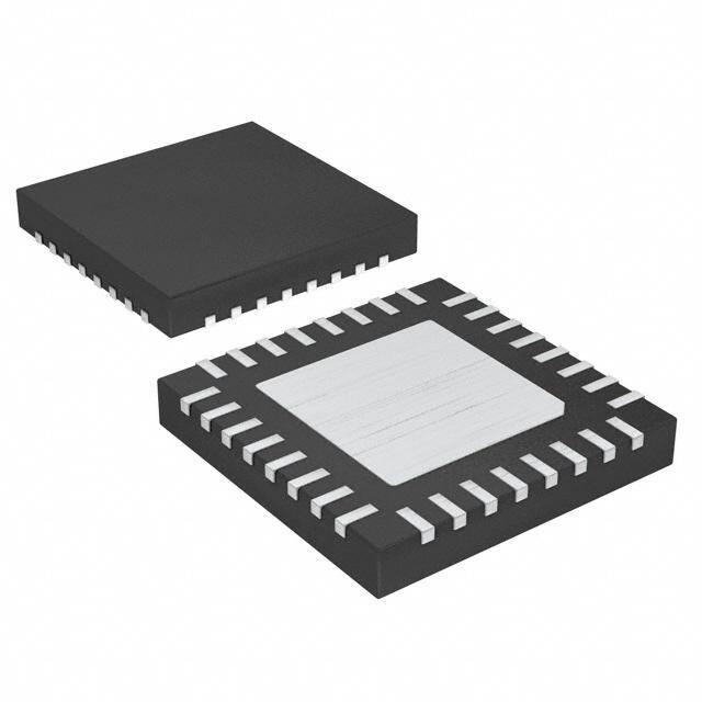
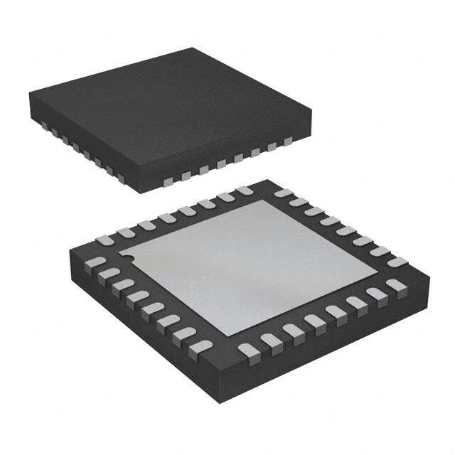
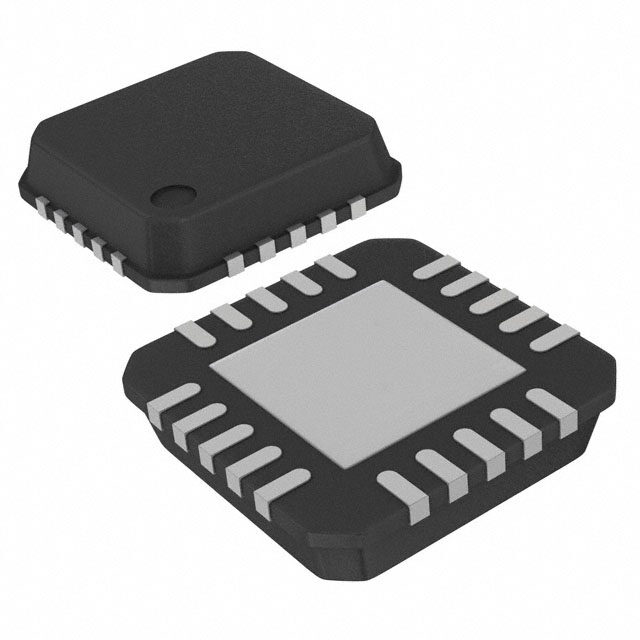
| 描述 | IC CLK BUFFER 3:10 200MHZ 32QFN时钟缓冲器 1:10 LVCMOS FANOUT BUFFER |
| 产品分类 | |
| 品牌 | ON Semiconductor |
| 产品手册 | |
| 产品图片 |
|
| rohs | 符合RoHS无铅 / 符合限制有害物质指令(RoHS)规范要求 |
| 产品系列 | 时钟和计时器IC,时钟缓冲器,ON Semiconductor NB3F8L3010CMNG- |
| mouser_ship_limit | 该产品可能需要其他文件才能进口到中国。 |
| 数据手册 | |
| 产品型号 | NB3F8L3010CMNG |
| 产品种类 | 时钟缓冲器 |
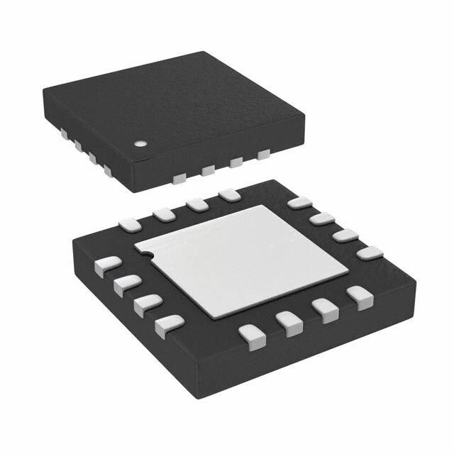
| 供应商器件封装 | 32-QFN(5x5) |
| 其它名称 | NB3F8L3010CMNG-ND |
| 包装 | 管件 |
| 商标 | ON Semiconductor |
| 安装类型 | 表面贴装 |
| 安装风格 | SMD/SMT |
| 封装 | Tube |
| 封装/外壳 | 32-VFQFN 裸露焊盘 |
| 封装/箱体 | QFN-32 |
| 工作温度 | -40°C ~ 85°C |
| 工厂包装数量 | 74 |
| 差分-输入:输出 | 是/无 |
| 最大工作温度 | + 85 C |
| 最大输入频率 | 40 MHz |
| 最小工作温度 | - 40 C |
| 标准包装 | 74 |
| 比率-输入:输出 | 3:10 |
| 电压-电源 | 2.375 V ~ 3.465 V |
| 电源电压-最大 | 3.3 V |
| 电源电压-最小 | 1.5 V |
| 电源电流 | 50 mA |
| 电路数 | 1 |
| 类型 | 扇出缓冲器(分配),多路复用器 |
| 系列 | NB3F8L3010C |
| 输入 | HCSL,LVDS,LVPECL,SSTL,晶体 |
| 输出 | LVCMOS,LVTTL |
| 频率-最大值 | 200MHz |


- 商务部:美国ITC正式对集成电路等产品启动337调查
- 曝三星4nm工艺存在良率问题 高通将骁龙8 Gen1或转产台积电
- 太阳诱电将投资9.5亿元在常州建新厂生产MLCC 预计2023年完工
- 英特尔发布欧洲新工厂建设计划 深化IDM 2.0 战略
- 台积电先进制程称霸业界 有大客户加持明年业绩稳了
- 达到5530亿美元!SIA预计今年全球半导体销售额将创下新高
- 英特尔拟将自动驾驶子公司Mobileye上市 估值或超500亿美元
- 三星加码芯片和SET,合并消费电子和移动部门,撤换高东真等 CEO
- 三星电子宣布重大人事变动 还合并消费电子和移动部门
- 海关总署:前11个月进口集成电路产品价值2.52万亿元 增长14.8%


PDF Datasheet 数据手册内容提取
3.3V / 2.5V / 1.8V / 1.5V 3:1:10 LVCMOS Fanout Buffer NB3F8L3010C Description The NB3F8L3010C is a 3:1:10 Clock / Data fanout buffer operating on a 3.3 V / 2.5 V Core VDD and two flexible 3.3 V / 2.5 V / 1.8 V / www.onsemi.com 1.5 V VDDO supplies which must be equal or less than V . n DD A Mux selects between a Crystal input, or either of two differential/SE Clock / Data inputs. Differential Inputs accept MARKING LVPECL, LVDS, HCSL, or SSTL and Single−Ended levels. The DIAGRAM MUX control lines, SEL0 and SEL1, select CLK0/CLK0, 1 CLK1/CLK1, or Crystal input pins per Table 3. The Crystal input is 1 32 NB3F8L disabled when a Clock input is selected. Output enable pin, OE, 3010C QFN32 synchronously forces a High Impedance state (HZ) when Low per AWLYYWWG G SUFFIX Table 4. CASE 488AM Outputs consist of 10 single−ended LVCMOS outputs. A = Assembly Location Features WL = Wafer Lot • Ten CMOS / LVTTL Outputs up to 200 MHz YY = Year • WW = Work Week Differential Inputs Accept LVPECL, LVDS, HCSL, or SSTL • G = Pb−Free Package Crystal Oscillator Interface • Crystal Input Frequency Range: 10 MHz to 50 MHz • ORDERING INFORMATION Output Skew: 10 ps Typical See detailed ordering and shipping information page 12 of this • Additive RMS Phase Jitter @ 125 MHz, (12 kHz – 20 MHz): 0.03 ps data sheet. (Typical) • Synchronous Output Enable • Output Defined Level When Input is Floating • Power Supply Modes: ♦ Single 3.3 V ♦ Single 2.5 V ♦ Mixed 3.3 V ± 5% Core/2.5 V ± 5% Output Operating Supply ♦ Mixed 3.3 V ± 5% Core/1.8 V ± 0.2 V Output Operating Supply ♦ Mixed 3.3 V ± 5% Core/1.5 V ± 0.15 V Output Operating Supply ♦ Mixed 2.5 V ± 5% Core/ 1.8 V ± 0.2 V Output Operating Supply ♦ Mixed 2.5 V ± 5% Core /1.5 V ± 0.15 V Output Operating Supply • Two Separate Output Bank Power Supplies • Industrial temp. range -40°C to 85°C • These are Pb−Free Devices Applications • Clock Distribution • Networking and Communications • High End Computing • Wireless and Wired Infrastructure End Products • Servers • Ethernet Switch/Routers • ATE • Test and Measurement © Semiconductor Components Industries, LLC, 2016 1 Publication Order Number: December, 2019 − Rev. 8 NB3F8L3010C/D
NB3F8L3010C BANK A VDD Q0 VDDOA VDDOB Q1 GND SEL0 Q2 SEL1 CLK0 Q3 CLK0 Q4 CLK1 CLK1 XTAL_IN BANK B OSC XTAL_OUT Q5 Q6 Q7 Q8 Q9 OE SYNC Figure 1. Simplified Logic Diagram GND OE SEL0 SEL1 CLK1 CLK1 GND GND Exposed Pad (EP) 2 1 0 9 8 7 6 5 3 3 3 2 2 2 2 2 Q0 1 24 Q9 VDDOA 2 23 VDDOB Q1 3 22 Q8 GND 4 21 GND NB3F8L3010C Q2 5 20 Q7 VDDOA 6 19 VDDOB Q3 7 18 Q6 Q4 8 17 Q5 9 10 11 12 13 14 15 16 GND VDD AL_IN _OUT CLK0 CLK0 GND GND T L X A T X Figure 2. Pinout Configuration (Top View) www.onsemi.com 2
NB3F8L3010C Table 1. PIN DESCRIPTION Input Number Name Type Default Description 1, 3, 5, 7, Q0, Q1, Q2, LVCMOS Outputs − Bank A 8 Q3, Q4 17, 18, Q5, Q6, Q7, LVCMOS Outputs − Bank B 20, 22, 24 Q8, Q9 2, 6 VDDOA Power Positive Supply Pins for Bank A Outputs Q0 − Q4 19, 23 VDDOB Power Positive Supply Pins for Bank B Outputs Q5 − Q9 4, 9, 15, GND GND Ground Supply 16, 21, 25, 26, 32 10 VDD Power VDD Positive Supply pin for Core and Inputs. 11 XTAL_IN XTAL OSC / CLK Input Crystal Oscillator Interface or External Clock Source at LVCMOS Levels 12 XTAL_OUT XTAL OSC Output Crystal Oscillator Interface 13 CLK0 Diff / SE Input Pulldown Non-inverting clock/data input 0. 14 CLK0 Diff / SE Input Pullup / Inverting differential clock input 0. Pulldown 27 CLK1 Diff / SE Input Pullup / Inverting differential clock input 1 Pulldown 28 CLK1 Diff / SE Input Pulldown Non-inverting clock/data input 1 29 SEL1 LVCMOS / LVTTL Pulldown Input clock select. See Table 3 for function. Input Pulldown Input 30 SEL0 LVCMOS / LVTTL Pulldown Input clock select. See Table 3 for function. Input Pulldown Input 31 OE LVCMOS / LVTTL Pulldown Output Enable Control. See Table 4 for function. Input − EP − The Exposed Pad (EP) on the QFN−32 package bottom is thermally connected to the die for improved heat transfer out of package. The exposed pad must be attached to a heat− sinking conduit. The pad is electrically connected to the die, and must be electrically connected to GND. 1. All VDD, VDDOn and GND pins must be externally connected to a power supply to guarantee proper operation. Bypass each VDD and VDDOn with 0.01 (cid:2)F CAP to GND. Table 2. PIN CHARACTERISTICS Symbol Parameter Min Typ Max Unit CIN Input Capacitance 4 pF R Input Pulldown Resistor; Input Pulldown Resistor 50 k(cid:3) CPD Power Dissipation Capacitance (per output) pF VDDO = 3.3 V VDDO = 2.5 V VDDO = 1.8 V VDDO = 1.5 V ROUT Output Impedance (cid:3) VDDO = 3.3 V VDDO = 2.5 V VDDO = 1.8 V 20 VDDO = 1.5 V www.onsemi.com 3
NB3F8L3010C FUNCTION TABLES Table 3. CLOCK ENABLE (SELx) FUNCTION TABLE Table 5. DIFF IN/OUT TABLE (Diff or S.E.) SEL[1:0] Input Selected Input Clock Input Condition Output 00 CLK0/CLK0 CLK0/1; CLK0/1 = OPEN Logic LOW 01 CLK1/CLK1 CLK0/1; CLK0/1 = GND Undefined 10 Crystal Osc Input CLK0/1 = HIGH; CLK0/1 = LOW Logic HIGH 11 Crystal Osc Input CLK0/1 = LOW; CLK0/1 = HIGH Logic LOW Table 4. CLOCK OUTPUT ENABLE (OE) FUNCTION TABLE OE Input Q[9:0] Output 0 High Impedance 1 Outputs Enabled Table 6. CRYSTAL CHARACTERISTICS Parameter Min Typ Max Unit Mode of Oscillation Fundamental Frequency 10 50 MHz Equivalent Series Resistance (ESR) 50 (cid:3) Shunt Capacitance 7 pF Drive Power 100 (cid:2)W Table 7. ATTRIBUTES Characteristic Value ESD Protection Human Body Model >2 kV Machine Model 200 V Moisture Sensitivity (Note 2) QFN32 Level 1 Flammability Rating Oxygen Index: 28 to 34 UL 94 V−0 @ 0.125 in Transistor Count 474 Devices Meets or exceeds JEDEC Spec EIA/JESD78 IC Latchup Test 2. For additional information, see Application Note AND8003/D. Table 8. MAXIMUM RATINGS (Note 3) Symbol Parameter Condition Rating Unit VDD, Positive Power Supply GND = 0 V 4.6 V VDDOn VI Input Voltage V XTAL_IN 0 (cid:2) VI (cid:2) VDD Diff, SELx, OE Inputs –0.5 (cid:2) VI (cid:2) VDD + 0.5 VO Output Voltage – 0.5 (cid:2) VO (cid:2) VDDOn + 0.5 V TA Operating Temperature Range, Industrial −40 to +85 (cid:2)C Tstg Storage Temperature Range −65 to +150 (cid:2)C θJA Thermal Resistance (Junction−to−Ambient) 0 lfpm 31 (cid:2)C/W 500 lfpm 27 θJC Thermal Resistance (Junction−to−Case) (Note 3) 12 (cid:2)C/W Stresses exceeding those listed in the Maximum Ratings table may damage the device. If any of these limits are exceeded, device functionality should not be assumed, damage may occur and reliability may be affected. 3. JEDEC standard multilayer board − 2S2P (2 signal, 2 power). www.onsemi.com 4
NB3F8L3010C Table 9. POWER SUPPLY DC CHARACTERISTICS VDD = 3.3 V ± 5% (3.135 V to 3.465 V) or VDD = 2.5 V ±5% (2.375 V to 2.625 V) and VDDOn = 3.3 V ± 5% (3.135 V to 3.465 V) or 2.5 V ± 5% (2.375 V to 2.625 V) or 1.8 V ± 0.2 V (1.6 V to 2.0 V) or 1.5 V ± 0.15 V (1.35 V to 1.65 V); TA = −40°C to 85°C Symbol Parameter Test Conditions Min Typ Max Unit IDD VDD Power Supply OE = 0, no load 30 50 mA Current 3.3 V ± 5%; VDDOn = 3.3 V ± 5% or 2.5 V ± 5% or 1.8 V ± 0.2 V or 1.5 V ± 0.15 V 2.5 V ± 5%; VDDOn = 2.5 V ± 5% or 1.8 V ± 0.2 V or 1.5 V ± 0.15 V IDDO VDDO Power Supply OE = 0, no load 5 mA Current 3.3 V ± 5%; VDDOn = 3.3 V ± 5% or 2.5 V ± 5% or 1.8 V ± 0.2 V or 1.5 V ± 0.15 V 2.5 V ± 5%; VDDOn = 2.5 V ± 5% or 1.8 V ± 0.2 V or 1.5 V ± 0.15 V NOTE:Device will meet the specifications after thermal equilibrium has been established when mounted in a test socket or printed circuit board with maintained transverse airflow greater than 500 lfpm. Table 10. DC CHARACTERISTICS TA = −40°C to 85°C Symbol Parameter Test Conditions Min Typ Max Unit VIH LVCMOS / LVTTL Input High Voltage VDD = 3.3 V ±5% 2 VDD + 0.3 V (OE, SELx) VDD = 2.5 V ± 5% 1.7 VDD + 0.3 VIL LVCMOS / LVTTL Input Low Voltage VDD = 3.3 V ±5% −0.3 0.8 V (OE, SELx) VDD = 2.5 V ± 5% −0.3 0.7 IIH Input High Current (cid:2)A OE, SELx, VDD = VIN = 3.465 V 150 CLKx/CLKx VDD = VIN = 3.465 V or 2.625 V 150 IIL Input Low Current (cid:2)A OE, SELx VDD = 3.465 V; VIN = 0.0 V −5 CLKx VDD = 3.465 V or 2.625 V VIN = 0.0 V −5 CLKx VDD = 3.465 V or 2.625 V VIN = 0.0 V −150 VOH Output High Voltage (Note 4) VDDOn = 3.3 V ± 5% 2.6 V VDDOn = 2.5 V ± 5% 1.8 VDDOn = 1.8 V ± 0.2 V 1.2 VDDOn = 1.5 V ± 0.15 V 0.9 VOL Output Low Voltage (Note 4) VDDOn = 3.3 V ± 5% or 2.5 V ± 5% 0.5 V VDDOn = 1.8 V ± 0.2 V 0.4 VDDOn = 1.5 V ± 0.15 V 0.37 VPP Peak−to−Peak Input Voltage VDD = 3.3 V ±5% or VDD = 2.5 V ± 5% 0.15 1.3 V VIL > −0.3 V CLKx/CLKx VIHCMR Input High Level Common Mode VDD = 3.3 V ±5% or VDD = 2.5 V ± 5% 0.5 VDD − 0.85 V Range VCM = VIH; VIL > −0.3 V CLKx/CLKx NOTE:Device will meet the specifications after thermal equilibrium has been established when mounted in a test socket or printed circuit board with maintained transverse airflow greater than 500 lfpm. 4. Outputs terminated with 50 (cid:3) to VDDOn/2. See Parameter Measurement Information.. Table 11. AC CHARACTERISTICS VDD = 3.3 V ± 5% (3.135 V to 3.465 V) or VDD = 2.5 V ±5% (2.375 V to 2.625 V) and VDDOn = 3.3 V ± 5% (3.135 V to 3.465 V) or 2.5 V ± 5% (2.375 V to 2.625 V) or 1.8 V ± 0.2 V (1.6 V to 2.0 V) or 1.5 V ± 0.15 V (1.35 V to 1.65 V); TA = −40°C to 85°C Symbol Parameter Test Conditions Min Typ Max Unit fMAX Output Frequency Using External 10 50 MHz Crystal Using External DC 200 MHz Clock Source (Note 5) www.onsemi.com 5
NB3F8L3010C Table 11. AC CHARACTERISTICS VDD = 3.3 V ± 5% (3.135 V to 3.465 V) or VDD = 2.5 V ±5% (2.375 V to 2.625 V) and VDDOn = 3.3 V ± 5% (3.135 V to 3.465 V) or 2.5 V ± 5% (2.375 V to 2.625 V) or 1.8 V ± 0.2 V (1.6 V to 2.0 V) or 1.5 V ± 0.15 V (1.35 V to 1.65 V); TA = −40°C to 85°C Symbol Parameter Test Conditions Min Typ Max Unit tsk(o) Output Skew (Notes 6 and 7) 10 55 ps tJITTER(cid:4) Additive RMS Input clock from VDDOn = 3.3 V ± 5% 0.03 ps Phase Jitter CLK0/CLK0 or (Integrated CLK1/CLK1 VDDOn = 2.5 V ± 5% 0.03 1202 MkHHzz (cid:3)) VDDOn = 1.8 V ± 0.2 V 0.03 (Note 8) VDDOn = 1.5 V ± 0.15 V 0.03 External clock VDDOn = 3.3 V ± 5% 0.03 over drives crystal interface VDDOn = 2.5 V ± 5% 0.03 VDDOn = 1.8 V ± 0.2 V 0.03 VDDOn = 1.5 V ± 0.15 V 0.03 Input clock from VDDOn = 3.3 V ± 5% 0.03 crystal VDDOn = 2.5 V ± 5% 0.03 VDDOn = 1.8 V ± 0.2 V 0.03 VDDOn = 1.5 V ± 0.15 V 0.03 tR / tF Output Rise/Fall Time (20% and 80%) VDDOn = 3.3 V ± 5% 150 350 500 ps VDDOn = 2.5 V ± 5% 150 350 500 VDDOn = 1.8 V ± 0.2 V 150 350 600 VDDOn = 1.5 V ± 0.15 V 150 350 600 odc Output Duty Cycle VDDOn = 3.3 V ± 5% 45 55 % VDDOn = 2.5 V ± 5% 40 60 VDDOn = 1.8 V ± 0.2 V 40 60 VDDOn = 1.5 V ± 0.15 V 40 60 tEN Output Enable OE 4 cycles Time (Note 9) tDIS Output Disable OE 4 cycles Time (Note 9) MUX_ISOLATION MUX_ISOLATION 155.52 MHz 55 dB NOTE:Device will meet the specifications after thermal equilibrium has been established when mounted in a test socket or printed circuit board with maintained transverse airflow greater than 500 lfpm. 5. XTAL_IN can be overdriven relative to a signal a crystal would provide. 6. Defined as skew between outputs at the same supply voltage and with equal load conditions. Measured at VDDOn/2. 7. This parameter is defined in accordance with JEDEC Standard 65. 8. See phase noise plot. 9. These parameters are guaranteed by characterization. Not tested in production. See Parameter Measurement Information www.onsemi.com 6
NB3F8L3010C PARAMETER MEASUREMENT INFORMATION VDD = +1.65 V ±5% VDD = +1.25 V ±5% VDDOn = VDD = +1.65 V ±5% SCOPE VDDOn = VDD = +1.25 V ±5% SCOPE Qx Qx LVCMOS Z = 50 (cid:3) LVCMOS Z = 50 (cid:3) 50 (cid:3) 50 (cid:3) GND = +1.65 V ±5% GND = +1.25 V ±5% 3.3 V Core / 3.3 V Output Load AC Test Circuit 2.5 V Core / 2.5 V Output Load AC Test Circuit (Terminating to VDDOn/2) (Terminating to VDDOn/2) VDD = +2.05 V ±5% VDD = +2.4 V ±5% VDDOn = +1.25 V ±5% SCOPE VDDOn = +0.9 V ±0.1 V SCOPE Qx Qx LVCMOS Z = 50 (cid:3) LVCMOS Z = 50 (cid:3) 50 (cid:3) 50 (cid:3) GND = +1.25 V ±5% GND = +0.9 V ±0.1 V 3.3 V Core / 2.5 V Output Load AC Test Circuit 3.3 V Core / 1.8 V Output Load AC Test Circuit (Terminating to VDDOn/2) (Terminating to VDDOn/2) VDD = +2.55 V ±5% VDD = +1.6 V ±5% VDDOn = +0.75 V ±0.15 V SCOPE VDDOn = +0.9 V ±0.1 V SCOPE Qx Qx LVCMOS Z = 50 (cid:3) LVCMOS Z = 50 (cid:3) 50 (cid:3) 50 (cid:3) GND = +0.75 V ±0.15 V GND = +0.9 V ±0.1 V 3.3 V Core / 1.5 V Output Load AC Test Circuit 2.5 V Core / 1.8 V Output Load AC Test Circuit (Terminating to VDDOn/2) (Terminating to VDDOn/2) VDD = +1.75 V ±5% VDDOn = +0.75 V ±0.15 V SCOPE Qx LVCMOS Z = 50 (cid:3) 50 (cid:3) GND = +0.75 V ±0.5 V 2.5 V Core / 1.5 V Output Load AC Test Circuit (Terminating to VDDOn/2) Figure 3. Operational Supply and Termination Test Conditions www.onsemi.com 7
NB3F8L3010C PARAMETER MEASUREMENT INFORMATION VDD VDDOn/2 Qx CLK VPP Xpoint VCMR CLK VDDOn/2 GND Qv tsk(0) Differential Input Level Within Device Output Skew VDD VDD/2 OE 0 V VDDOn/2 tEN tDIS VOH Qx tPW Qx VDDOn/2 VDDOn/2VOL odc = (tPW / tPeriod) x 10tP0e%riod Output Enable /Disable Output Duty Cycle / Pulse Width / Period (OE HIGH = Enabled) Spectrum of Output Signal Qx MUX selects 80% 80% B) A0 active input clock e (d MUX(cid:2) _ISOL= A0- A1 signal d MUX selects u A1 Qx 20% 20% mplit static input tR tF A Output Rise/Fall Time Frequency (Hz) fc (Fundamental) MUX Isolation Figure 4. Operational Waveforms and MUX Input Isolation Plot APPLICATION INFORMATION Recommendations for Unused LVCMOS Output Pins LVCMOS Control Pins All control pins have internal pulldowns; additional Inputs: resistance is not required but can be added for additional protection. A 1 k(cid:3) resistor can be used. CLK/CLK Inputs For applications not requiring the use of the differential Power Supplies input, both CLK and CLK can be left floating. Though not VDD is the power supply for the core and input circuitry. required, but for additional protection, a 1 k(cid:3) resistor can be VDDOA and VDDOB are two separate positive power tied from CLK to ground. supplies for two banks of outputs: Crystal Inputs VDDOA pins 2 and 6 are connected internally for outputs For applications not requiring the use of the crystal Q0 − Q4. oscillator input, both XTAL_IN and XTAL_OUT can be left VDDOB pins 19 and 23 are connected internally for outputs floating. Though not required, but for additional protection, Q5 − Q9. a 1 k(cid:3) resistor can be tied from XTAL_IN to ground. LVCMOS Outputs A 33 (cid:3) series terminating resistor may be used on each clock output if the trace is longer than 1 inch. www.onsemi.com 8
NB3F8L3010C Differential Input with Single−Ended Interconnect amplitude in half. Termination may be done by using Rs or Refer to Figure 5 to interconnect a single−ended to a by using R1 and R2. First, Rs = 0 and then R3 and R4 in Differential Pair of inputs. The reference bias voltage VREF parallel should equal the transmission line impedance. For = VDD/2 is generated by the resistor divider of R3 and R4. most 50 (cid:3) applications, R1 and R2 can be 100 (cid:3). The Bypass capacitor (C1) can filter noise on the DC bias. This differential input can handle full rail LVCMOS signaling, bias circuit should be located as close to the input pin as but it is recommended that the amplitude be reduced. The possible. Adjust R1 and R2 to common mode voltage of the datasheet specifies a differential amplitude which needs to signal input swing to preserve duty cycle. be doubled for a single ended equivalent stimulus. V ILmin This configuration requires that the sum of the output cannot be less than −0.3 V and V cannot be more than IHmax impedance of the driver (Ro) and the series resistance (Rs) V + 0.3 V. The datasheet specifications are characterized DD equals the transmission line impedance. In addition, and guaranteed by using a differential signal. matched termination by R1 and R2 will attenuate the signal VDD VDD VDD R1 R3 Single Rs 100 (cid:3) 1 k(cid:3) CLKx Ended RO Zo = 50 (cid:3) Driver Z0 = RO + Rs Differential In R2 R4 CLKx 100 (cid:3) 1 k(cid:3) C0.11 (cid:2)F GND = 0.0 GND = 0.0 GND = 0.0 Figure 5. Differential Input with Single−ended Interconnect Crystal Input Interface CLOCK Overdriving the XTAL Interface The device has been characterized with 18 pF parallel The XTAL_IN input can accept a single−ended LVCMOS resonant crystals. The capacitor values, C1 and C2, shown signal through an AC coupling capacitor. A general in Figure 6 below as 15 pF were determined using an 18 pF LVCMOS interface diagram is shown in Figure 7 and a parallel resonant crystal and were chosen to minimize the general LVPECL interface in Figure 8. The XTAL_OUT ppm error. The optimum C1 and C2 values can be slightly pin must be left floating. The maximum amplitude of the adjusted for different board layouts. input signal should not exceed 2 V and the input edge rate can be as slow as 10 ns. This configuration requires that the output impedance of the driver (Ro) plus the series resistance (Rs) equals the transmission line impedance. In addition, matched termination at the crystal input will attenuate the signal in half. This can be done in one of two ways. First, R1 and R2 in parallel should equal the transmission line impedance. For most 50 (cid:3) applications, R1 and R2 can be 100 (cid:3). This can also be accomplished by removing R1 and making R2 50 (cid:3). By overdriving the crystal oscillator, the device will be functional, but note, the device performance is guaranteed by using a quartz crystal. Figure 6. Crystal Input Interface www.onsemi.com 9
NB3F8L3010C VDD VDD R1 C1 LVMOS Rs 100 (cid:3) 0.1 (cid:2)F RO Zo = 50 (cid:3) XTAL_IN Z0 = RO + Rs R2 100 (cid:3) XTAL_OUT GND = 0.0 V GND = 0.0 V Figure 7. General Diagram for LVCMOS Driver to XTAL Input Interface Use Rs or R1 / R2 VDD C1 0.1 (cid:2)F Zo = 50 (cid:3) XTAL_IN LVPECL Zo = 50 (cid:3) XTAL_OUT 50 (cid:3) 50 (cid:3) GND = 0.0 V VTT = VDD − 2.0 V Figure 8. General Diagram for LVPECL Driver to XTAL Input Interface www.onsemi.com 10
NB3F8L3010C Differential Clock Input Interface input interfaces suggested here are examples only. If the The CLK / CLK accept LVDS, LVPECL, SSTL, HCSL driver is from another vendor, use their termination differential signals. Signals must meet the VPP and VCMR recommendation. Please consult with the vendor of the input requirements. Figures 9 to 13 show interface driver component to confirm the driver termination examples for the CLK / CLK input with built−in 50 (cid:3) requirements. terminations driven by the most common driver types. The VDD = +3.3 V VDD = +3.3 V VDD = +3.3 V VDD = +3.3 V VDD = +3.3 V 125 (cid:3) 125 (cid:3) Qx CLKx Qx CLKx Zo = 50 (cid:3) Zo = 50 (cid:3) LVPECL Differential LVPECL Differential CLKx In CLKx In Zo = 50 (cid:3) Zo = 50 (cid:3) Qx 84 (cid:3) 84 (cid:3) Qx 50 (cid:3) 50 (cid:3) GND = 0.0 V GND = 0.0 V GND = 0.0 V GND = 0.0 V 50 (cid:3) GND = 0.0 V GND = 0.0 V Figure 9. CLK / CLK Input Driven by 3.3 V LVPECL Figure 10. CLK / CLK Input Driven by 3.3 V Driver (Thevenin Parallel Termination) LVPECL Driver (“Y” Parallel Termination) VDD = +3.3 V VDD = +3.3 V VDD = +3.3 V VDD = +3.3 V Qx 33 (cid:3) (Opt) CLKx Qx CLKx Zo = 50 (cid:3) Zo = 50 (cid:3) HCSL Differential LVDS 100 (cid:3) Differential CLKx In CLKx In Zo = 50 (cid:3) Zo = 50 (cid:3) Qx 33 (cid:3) (Opt) 50 (cid:3) 50 (cid:3) Qx GND = 0.0 V GND = 0.0 V GND = 0.0 V GND = 0.0 V GND = 0.0 V Figure 11. CLK / CLK Input Driven by a 3.3 V Figure 12. CLK / CLK Input Driven by 3.3 V HCSL Driver LVDS Driver VDD = +2.5 V VDD = +2.5 V VDD = +3.3 V 120 (cid:3) 120 (cid:3) Qx CLKx Zo = 50 (cid:3) SSTL Differential CLKx In Zo = 50 (cid:3) Qx 120 (cid:3) 120 (cid:3) GND = 0.0 V GND = 0.0 V GND = 0.0 V Figure 13. CLK / CLK Input Driven by 2.5 V SSTL Driver www.onsemi.com 11
NB3F8L3010C VFQFN EPAD Thermal Release Path to ground through these vias. The vias act as “heat pipes”. In order to maximize both the removal of heat from the The number of vias (i.e. “heat pipes”) is application specific package and the electrical performance, a land pattern must and dependent upon the package power dissipation as well be incorporated on the Printed Circuit Board (PCB) within as electrical conductivity requirements. Thus, thermal and the footprint of the package corresponding to the exposed electrical analysis and/or testing are recommended to metal pad or exposed heat slug on the package, as shown in determine the minimum number needed. Maximum thermal Figure 14. The solderable area on the PCB, as defined by the and electrical performance is achieved when an array of vias solder mask, should be at least the same size/shape as the is incorporated in the land pattern. It is recommended to use exposed pad/slug area on the package to maximize the as many vias connected to ground as possible. It is also thermal/electrical performance. Sufficient clearance should recommended that the via diameter should be 12 to 13 mils be designed on the PCB between the outer edges of the land (0.30 to 0.33 mm) with 1 oz copper via barrel plating. This pattern and the inner edges of pad pattern for the leads to is desirable to avoid any solder wicking inside the via during avoid any shorts. While the land pattern on the PCB provides the soldering process which may result in voids in solder a means of heat transfer and electrical grounding from the between the exposed pad/slug and the thermal land. package to the board through a solder joint, thermal vias are Precautions should be taken to eliminate any solder voids necessary to effectively conduct from the surface of the PCB between the exposed heat slug and the land pattern. Note: to the ground plane(s). The land pattern must be connected These recommendations are to be used as a guideline only. Figure 14. Suggested Assembly for Exposed Pad Thermal Release Path – Cut−away View (not to scale) ORDERING INFORMATION Device Package Shipping† NB3F8L3010CMNG QFN32 74 Units / Rail (Pb−Free) NB3F8L3010CMNR4G QFN32 1000 / Tape & Reel (Pb−Free) NB3F8L3010CMNTWG QFN32 1000 / Tape & Reel (Pb−Free) †For information on tape and reel specifications, including part orientation and tape sizes, please refer to our Tape and Reel Packaging Specifications Brochure, BRD8011/D. www.onsemi.com 12
NB3F8L3010C PACKAGE DIMENSIONS QFN32 5x5, 0.5P CASE 488EW ISSUE O D A NOTES: B 1. DIMENSIONS AND TOLERANCING PER ASME Y14.5M, 1994. PIN ONE ÉÉ 2. CONTROLLING DIMENSION: MILLIMETERS. LOCATION 3. DIMENSION b APPLIES TO PLATED TERMINAL AND IS MEASURED BETWEEN ÉÉ 0.15 AND 0.30MM FROM THE TERMINAL TIP. 4. COPLANARITY APPLIES TO THE EXPOSED E PAD AS WELL AS THE TERMINALS. MILLIMETERS DIM MIN MAX 0.15 C A 0.80 1.00 A1 −−− 0.05 A3 0.20 REF 0.15 C TOP VIEW b 0.18 0.30 D 5.00 BSC D2 2.95 3.25 A E 5.00 BSC 0.10 C (A3) E2 2.95 3.25 A1 e 0.50 BSC K 0.20 −−− L 0.30 0.50 0.08 C NOTE 4 SIDE VIEW C SPELAATNIENG RECOMMENDED SOLDERING FOOTPRINT* D2 K 5.30 9 32X 3.35 0.63 8 17 32X L 1 E2 1 3.35 5.30 32 25 32Xb e 0.10 M C A B e/2 0.05 M C NOTE 3 BOTTOM VIEW POAUCTKLAIGNEE 0.50 32X PITCH 0.30 DIMENSION: MILLIMETERS *For additional information on our Pb−Free strategy and soldering details, please download the ON Semiconductor Soldering and Mounting Techniques Reference Manual, SOLDERRM/D. ON Semiconductor and are trademarks of Semiconductor Components Industries, LLC dba ON Semiconductor or its subsidiaries in the United States and/or other countries. ON Semiconductor owns the rights to a number of patents, trademarks, copyrights, trade secrets, and other intellectual property. A listing of ON Semiconductor’s product/patent coverage may be accessed at www.onsemi.com/site/pdf/Patent−Marking.pdf. ON Semiconductor reserves the right to make changes without further notice to any products herein. ON Semiconductor makes no warranty, representation or guarantee regarding the suitability of its products for any particular purpose, nor does ON Semiconductor assume any liability arising out of the application or use of any product or circuit, and specifically disclaims any and all liability, including without limitation special, consequential or incidental damages. Buyer is responsible for its products and applications using ON Semiconductor products, including compliance with all laws, regulations and safety requirements or standards, regardless of any support or applications information provided by ON Semiconductor. “Typical” parameters which may be provided in ON Semiconductor data sheets and/or specifications can and do vary in different applications and actual performance may vary over time. All operating parameters, including “Typicals” must be validated for each customer application by customer’s technical experts. ON Semiconductor does not convey any license under its patent rights nor the rights of others. ON Semiconductor products are not designed, intended, or authorized for use as a critical component in life support systems or any FDA Class 3 medical devices or medical devices with a same or similar classification in a foreign jurisdiction or any devices intended for implantation in the human body. Should Buyer purchase or use ON Semiconductor products for any such unintended or unauthorized application, Buyer shall indemnify and hold ON Semiconductor and its officers, employees, subsidiaries, affiliates, and distributors harmless against all claims, costs, damages, and expenses, and reasonable attorney fees arising out of, directly or indirectly, any claim of personal injury or death associated with such unintended or unauthorized use, even if such claim alleges that ON Semiconductor was negligent regarding the design or manufacture of the part. ON Semiconductor is an Equal Opportunity/Affirmative Action Employer. This literature is subject to all applicable copyright laws and is not for resale in any manner. PUBLICATION ORDERING INFORMATION LITERATURE FULFILLMENT: TECHNICAL SUPPORT Email Requests to: orderlit@onsemi.com North American Technical Support: Europe, Middle East and Africa Technical Support: Voice Mail: 1 800−282−9855 Toll Free USA/Canada Phone: 00421 33 790 2910 ON Semiconductor Website: www.onsemi.com Phone: 011 421 33 790 2910 For additional information, please contact your local Sales Representative ◊ www.onsemi.com 13
Mouser Electronics Authorized Distributor Click to View Pricing, Inventory, Delivery & Lifecycle Information: O N Semiconductor: NB3F8L3010CMNR4G NB3F8L3010CMNG