ICGOO在线商城 > 集成电路(IC) > 数据采集 - 触摸屏控制器 > MTCH6301-I/ML

 Datasheet下载
- 型号: MTCH6301-I/ML
- 制造商: Microchip
- 库位|库存: xxxx|xxxx
- 要求:
| 数量阶梯 | 香港交货 | 国内含税 |
| +xxxx | $xxxx | ¥xxxx |
查看当月历史价格
查看今年历史价格
MTCH6301-I/ML产品简介:
ICGOO电子元器件商城为您提供MTCH6301-I/ML由Microchip设计生产,在icgoo商城现货销售,并且可以通过原厂、代理商等渠道进行代购。 MTCH6301-I/ML价格参考¥15.30-¥15.30。MicrochipMTCH6301-I/ML封装/规格:数据采集 - 触摸屏控制器, IC SCREEN CNTRL 44QFN。您可以下载MTCH6301-I/ML参考资料、Datasheet数据手册功能说明书,资料中有MTCH6301-I/ML 详细功能的应用电路图电压和使用方法及教程。
MTCH6301-I/ML 是 Microchip Technology 推出的一款数据采集 - 触摸屏控制器,适用于电容式触摸屏应用。以下是其主要应用场景:

 1. 消费电子设备
   - 智能手机和平板电脑:支持多点触控功能,能够实现流畅的滑动、缩放和点击操作。
   - 家用电器:如智能冰箱、微波炉、洗衣机等,提供直观的触摸控制界面,取代传统机械按钮。
   - 遥控器:用于电视、音响等设备的遥控器,提升用户体验。

 2. 工业自动化
   - 人机界面 (HMI):在工业控制面板中,用于操作员与设备之间的交互,提供清晰、灵敏的触摸体验。
   - 仪器仪表:如便携式测量设备、示波器等,支持触摸屏操作以简化设置和数据分析。

 3. 医疗设备
   - 患者监护仪:用于触摸屏界面,方便医护人员快速调整参数。
   - 超声设备:支持高精度触摸操作,便于医生进行图像调节和诊断。
   - 便携式医疗设备:如血糖仪、血压计等,提供简单易用的触摸屏界面。

 4. 汽车电子
   - 车载信息娱乐系统:用于导航、音乐播放和空调控制等功能的触摸屏操作。
   - 仪表盘显示:支持触摸交互,使驾驶员能够更方便地访问车辆信息。

 5. 零售与服务行业
   - POS 终端:用于收银机和支付终端,支持快速、准确的操作。
   - 自助服务终端:如自动售货机、取票机等,提供用户友好的触摸屏界面。

 6. 教育与办公设备
   - 电子白板:支持多点触控功能,适合教学和会议场景。
   - 平板电脑和笔记本电脑:用于教育和办公领域,提供高效的操作体验。

 特性优势
- 支持多种屏幕尺寸和分辨率。
- 高抗噪能力,确保在复杂电磁环境下稳定运行。
- 超低功耗设计,延长电池寿命。
- 集成 I2C 和 SPI 接口,易于与其他系统组件集成。

综上所述,MTCH6301-I/ML 广泛应用于需要高灵敏度、可靠性和低功耗的触摸屏控制场景,为各类设备提供卓越的用户体验。
| 参数 | 数值 |
| 产品目录 | |
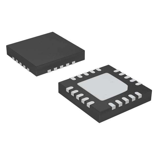
| 描述 | IC TOUCH CTRLR 44QFN电容触摸传感器 32KB Flash 8KB RAM, 40 MHz |
| 产品分类 | 电容式触摸传感器,接近传感器 IC电容触摸传感器 |
| 品牌 | Microchip Technology |
| 产品手册 | |
| 产品图片 | |
| rohs | 符合RoHS无铅 / 符合限制有害物质指令(RoHS)规范要求 |
| 产品系列 | Microchip Technology MTCH6301-I/ML* |
| 数据手册 | http://www.microchip.com/mymicrochip/filehandler.aspx?ddocname=en560085http://www.microchip.com/mymicrochip/filehandler.aspx?ddocname=en560084 |
| 产品型号 | MTCH6301-I/ML |
| PCN组件/产地 | 点击此处下载产品Datasheethttp://www.microchip.com/mymicrochip/NotificationDetails.aspx?id=5928&print=viewhttp://www.microchip.com/mymicrochip/NotificationDetails.aspx?id=6011&print=view |
| PCN设计/规格 | http://www.microchip.com/mymicrochip/NotificationDetails.aspx?id=5845&print=view |
| 产品种类 | 电容触摸传感器 |
| 商标 | Microchip Technology |
| 封装 | Tube |
| 工厂包装数量 | 45 |
| 标准包装 | 45 |


- 商务部:美国ITC正式对集成电路等产品启动337调查
- 曝三星4nm工艺存在良率问题 高通将骁龙8 Gen1或转产台积电
- 太阳诱电将投资9.5亿元在常州建新厂生产MLCC 预计2023年完工
- 英特尔发布欧洲新工厂建设计划 深化IDM 2.0 战略
- 台积电先进制程称霸业界 有大客户加持明年业绩稳了
- 达到5530亿美元!SIA预计今年全球半导体销售额将创下新高
- 英特尔拟将自动驾驶子公司Mobileye上市 估值或超500亿美元
- 三星加码芯片和SET,合并消费电子和移动部门,撤换高东真等 CEO
- 三星电子宣布重大人事变动 还合并消费电子和移动部门
- 海关总署:前11个月进口集成电路产品价值2.52万亿元 增长14.8%


PDF Datasheet 数据手册内容提取
MTCH6301 MTCH6301 Projected Capacitive Touch Controller Description: Touch Features: MTCH6301 is a turnkey projected capacitive controller • Multi-touch (up to ten touches) that allows easy integration of multi-touch and gestures • Gesture Detection and Reporting to create a rich user interface in your design. Through • Single and Dual Touch Drawing a sophisticated combination of Self and Mutual • Self and Mutual Signal Acquisition Capacitive scanning for both XY screens and touch • Built-in Noise Detection and Filtering pads, the MTCH6301 allows designers to quickly and easily integrate projected capacitive touch into their Power Management: application. • Configurable Sleep mode Applications: • Integrated Power-on Reset and Brown-out Reset • 200 µA Sleep Current (typical) • Human-Machine Interfaces with Configurable Button, Keypad or Scrolling Functions Communication Interface: • Single-Finger Gesture-Based Interfaces to Swipe, Scroll or Doubletap Controls • I2C™ (up to 400 kbps) • Home Automation Control Panels • Security Control Keypads Operating Conditions: • Automotive Center Stack Controls • 2.4V to 3.6V, -40ºC to +105ºC • Gaming Devices • Remote Control Touch Pads Package Types: Touch Sensor Support: • 44-Lead TQFP • 44-Lead QFN • Up to 13RX x 18TX Channels • Individual Channel Tuning for Optimal Sensitivity • Works with Printed Circuit Board (PCB) Sensors, Film, Glass and Flexible Printed Circuit (FPC) Sensors • Cover Layer Support: - Plastic: up to 3 mm - Glass: up to 5 mm Touch Performance: • > 100 Reports per Second Single Touch • > 60 Reports per Second Dual Touch • Up to 12-Bit Resolution Coordinate Reporting 2012-2014 Microchip Technology Inc. DS40001663B-page 1
MTCH6301 Table of Contents 1.0 System Block Diagram.................................................................................................................................................................3 2.0 Configuration and Setup...............................................................................................................................................................3 3.0 Pin Diagram..................................................................................................................................................................................4 4.0 Pinout I/O Descriptions.................................................................................................................................................................5 5.0 Layout...........................................................................................................................................................................................6 6.0 Communication Protocol............................................................................................................................................................12 7.0 Memory Map..............................................................................................................................................................................21 8.0 Special Features........................................................................................................................................................................23 9.0 Electrical Characteristics............................................................................................................................................................26 10.0 Ordering Information..................................................................................................................................................................30 11.0 Packaging Information................................................................................................................................................................31 The Microchip Web Site........................................................................................................................................................................ 38 Customer Change Notification Service................................................................................................................................................. 38 Customer Support................................................................................................................................................................................ 38 Worldwide Sales and Service............................................................................................................................................................... 40 TO OUR VALUED CUSTOMERS It is our intention to provide our valued customers with the best documentation possible to ensure successful use of your Microchip products. To this end, we will continue to improve our publications to better suit your needs. Our publications will be refined and enhanced as new volumes and updates are introduced. If you have any questions or comments regarding this publication, please contact the Marketing Communications Department via E-mail at docerrors@microchip.com. We welcome your feedback. Most Current Data Sheet To obtain the most up-to-date version of this data sheet, please register at our Worldwide Web site at: http://www.microchip.com You can determine the version of a data sheet by examining its literature number found on the bottom outside corner of any page. The last character of the literature number is the version number, (e.g., DS30000000A is version A of document DS30000000). Errata An errata sheet, describing minor operational differences from the data sheet and recommended workarounds, may exist for current devices. As device/documentation issues become known to us, we will publish an errata sheet. The errata will specify the revision of silicon and revision of document to which it applies. To determine if an errata sheet exists for a particular device, please check with one of the following: • Microchip’s Worldwide Web site; http://www.microchip.com • Your local Microchip sales office (see last page) When contacting a sales office, please specify which device, revision of silicon and data sheet (include literature number) you are using. Customer Notification System Register on our web site at www.microchip.com to receive the most current information on all of our products. DS40001663B-page 2 2012-2014 Microchip Technology Inc.
MTCH6301 1.0 SYSTEM BLOCK DIAGRAM FIGURE 1-1: SYSTEM BLOCK DIAGRAM MTCH6301 Touch Sensor User Configuration Data C o m m unications Engine GeMstDuulertcieTo oEdnuegchin e Noise Reduction / Filtering En Signal Acquisition Contro ADCTX DriSveeRnXs e TRXX00....1172 I2CTM gin lle Module e r [Master Controller] Touch Data MICROCHIP USB PICkitTM Serial Analyzer Connection only for initial tuning or configuration 2.0 CONFIGURATION AND SETUP The MTCH6301 is preconfigured for a 12Receiver(RX)/9 Transmitter (TX) touch sensor, mapped as shown in Section5.1 “Typical Application Circuit”. While the device will work out-of-the-box using this specific sensor configuration, most applications will require additional configuration and sensor tuning to determine the correct set of parameters to be used in the final application. Microchip provides a PC-based configuration tool for this purpose, available in the mTouch™ Sensing Solution Design Center (www.microchip.com/mtouch). Use of this tool requires a PICkit™ Serial Analyzer (updated with MTCH6301 support), as well as access to the I2C communications bus of the MTCH6301 device. Once the development process is complete, this modified parameter set must either be written permanently to the controller via NVRAM (see Section8.3 “Nonvolatile RAM (NVRAM)”), or alternatively, it can be sent every time the system is powered on. Both the PICkit Serial Analyzer and the master I2C controller can be used for this purpose. 2012-2014 Microchip Technology Inc. DS40001663B-page 3
MTCH6301 3.0 PIN DIAGRAM FIGURE 3-1: 44-PIN TQFP, QFN(1,2) 10 CLX1X1X9 DD SSX5X6X7X8X4 STTTVVTTTTT 4 3 2 1 0 9 8 7 6 5 4 4 4 4 4 4 3 3 3 3 3 3 SDA 1 33 TX0 TX17 2 32 TX1 TX16 3 31 TX2 TX15 4 30 TX3 TX14 5 29 V MTCH6301 SS V 6 MTCH6301 28 V SS DD VCAP 7 27 RX0 INT 8 26 RX1 N/C 9 25 RX2 RX12 10 24 RX3 RX11 11 23 RX4 2 3 4 5 6 7 8 9 0 1 2 1 1 1 1 1 1 1 1 2 2 2 3209 S DT8765 X1X1X1RXVSVDSERXRXRXRX TTR E R Note1: All RX/TX are remappable. Refer to Section5.6 “Sensor Layout Configuration” for further information. 2: The metal plate at the bottom of the device is not connected to any pins and it is recommended to be connected to VSS externally. DS40001663B-page 4 2012-2014 Microchip Technology Inc.
MTCH6301 4.0 PINOUT I/O DESCRIPTIONS TABLE 4-1: PINOUT I/O DESCRIPTIONS Pin Name Pin Number Pin Type Description RESET 18 I/P Reset Device (active-low) SCL 44 I Synchronous Serial Clock Input/Output for I2C™ SDA 1 I/O Synchronous Serial Data Input/Output for I2C™ INT 8 O Interrupt (from MTCH6301 to master) for I2C™ RX0 27* I/O RX1 26 I/O RX2 25 I/O RX3 24 I/O RX4 23 I/O RX5 22 I/O RX Sense (or TX Drive) RX6 21 I/O (*RX0/RX12 cannot be used for TX Drive) RX7 20 I/O RX8 19 I/O RX9 15 I/O RX10 14 I/O RX11 11 I/O RX12 10* I/O TX0 33 O TX1 32 O TX2 31 O TX3 30 O TX4 34 O TX5 38 O TX6 37 O TX7 36 O TX8 35 O TX Drive TX9 41 O TX10 42 O TX11 43 O TX12 13 O TX13 12 O TX14 5 O TX15 4 O TX16 3 O TX17 2 O N/C 9 N/C No Connect VCAP 7 P CPU Logic Filter Capacitor Connection VDD 17, 28, 40 P Positive Supply for Peripheral Logic and I/O Pins Ground Reference for Logic and I/O Pins; VSS 6, 16, 29, 39 P This pin must be connected at all times. 2012-2014 Microchip Technology Inc. DS40001663B-page 5
MTCH6301 5.0 LAYOUT 5.1 Typical Application Circuit The following schematic portrays a typical application circuit, based on a 12RX/ 9TX touch sensor. FIGURE 5-1: TYPICAL APPLICATION CIRCUIT MICROCHIP VDD PICkitTMSerial Analyzer 0.1 µF 43210987654 SCL 44444333333 SDA 1 SCLX11X10TX9VDDVSSTX5TX6TX7TX8TX4 33 TX0 SDA TT TX0 GPIO/INT 2 32 TX17 TX1 3 31 TX16 TX2 Master I2CTM 4 TX15 TX3 30 Controller 567 TVXSS14 MTCH6301 VVDSDS 222987 VDD 0.1 µF 8 VCAP RX0 26 T 10 µF INT RX1 X 9 25 8 N/C RX2 RX0 RX11 10 24 RX12 RX3 11 23 RX11 RX4 TX13TX12RX10 RX9VSSVDDRESETRX8RX7 RX6RX5 23456789012 11111111222 VDD 20 k O 0.1 µF 5.2 Decoupling Capacitors 3. Handling high-frequency noise: If the board is experiencing high-frequency noise, The use of decoupling capacitors on power supply upward of tens of MHz, add a second ceramic-type pins, such as VDD and VSS, is required (see capacitor in parallel to the above-described decoupling Figure5-1). Consider the following criteria when using capacitor. The value of the second capacitor can be in decoupling capacitors: the range of 0.01 µF to 0.001 µF. Place this second 1. Value and type of capacitor: capacitor next to the primary decoupling capacitor. In A value of 0.1 µF (100 nF), 10-20V is recommended. high-speed circuit designs, consider implementing a The capacitor should be a low Equivalent Series decade pair of capacitances as close to the power and Resistance (low ESR) capacitor and have resonance ground pins as possible (for example, 0.1 µF in parallel frequency in the range of 20 MHz and higher. It is with 0.001 µF). further recommended that ceramic capacitors be used. 4. Maximizing performance: 2. Placement on the Printed Circuit Board: On the board layout from the power supply circuit, run The decoupling capacitors should be placed as close to the power and return traces to the decoupling the pins as possible. It is recommended that the capacitors first, and then to the device pins. This capacitors be placed on the same side of the board as ensures that the decoupling capacitors are first in the the device. If layout space is constrained, the capacitor power chain. It is equally important to keep the trace can be placed on another layer on the PCB and length between the capacitor and the power pins to a connected using a via. Please ensure that the trace minimum, thereby reducing PCB track inductance. length from the pin to the capacitor is less than one-quarter inch (6 mm) in length. DS40001663B-page 6 2012-2014 Microchip Technology Inc.
MTCH6301 5.3 Bulk Capacitors 5.5.4 OPERATION WITH AN LCD The use of a bulk capacitor is recommended to improve MTCH6301 has integrated algorithms to detect and power supply stability. Typical values range from 4.7 µF minimize the effects of noise, but proper care should to 47 µF. This capacitor should be located as close to always be taken in selecting an LCD and support the device as possible. components with a focus on reducing noise as much as possible. Since the interaction between the touch sensor and display is highly dependent upon the 5.4 Capacitor on Internal Voltage physical arrangement of the components, proper Regulator (VCAP) testing should always be executed with a fully A low ESR (1 ohm) capacitor is required on the VCAP integrated device. Please reference your projected pin, which is used to stabilize the internal voltage capacitive touch screen manufacturer’s integration regulator output. The VCAP pin must not be connected guide for additional design considerations. to VDD and must have a CEFC capacitor with at least a 6V rating, connected to ground. The type can be 5.6 Sensor Layout Configuration ceramic or tantalum. To properly configure a sensor from a physical layout standpoint, the following registers must be correctly 5.5 Touch Sensor Design set: Considerations • RX Pin Map/TX Pin Map 5.5.1 SENSOR PATTERNS AND PCB • RX Scaling Coefficient/TX Scaling Coefficient LAYOUT • Flip State With regard to touch sensor patterns, please refer to 5.6.1 RX/TX PIN MAP the mTouch Design Center (www.micro- chip.com/mtouch) for additional information on design- By default, the RX and TX pins are set as shown in the ing and laying out a touch sensor pattern, as well as Typical Application Circuit (see Section5.1 “Typical using the correct techniques for PCB trace routing. Application Circuit”). It is recommended to keep this layout if possible. If a different layout or a different 5.5.2 PROTOTYPING DESIGNS amount of sensor channels is required, the RX and TX pins are configured via the Pin Map register arrays. To Due to their complexity, touch sensor designs typically access these arrays, please reference Section6.0 require a thorough debugging phase to ensure a “Communication Protocol” and Section7.0 reliable product. If possible, it is suggested that flexible “Memory Map”. prototyping hardware be created with this in mind. A common example is providing external access to the The RX and TX lines are configurable for the purpose communication lines for quick test and tuning while of making trace routing and board layout more in-circuit. Microchip’s Projected Capacitive convenient. Please note that while RX pins can be Configuration Utility (PCU) and a configured PICkit used as TX pins instead, a single pin cannot be used Serial Analyzer can assist with early prototype as both an RX and a TX channel concurrently. The pin development. See the online Microchip MTCH6301 maps are comprised of Pin Map ID numbers, which are device page for these and other support materials. shown in Table5-1. 5.5.3 SENSOR OVERLAY MATERIAL To prevent saturation of sensor levels, a minimum 0.5mm plastic or glass overlay is required for proper operation of the device, even during a prototyping phase, even if this value is different than the final design. Note: At no time should the device be expected to respond correctly to a user touching a bare PCB sensor. 2012-2014 Microchip Technology Inc. DS40001663B-page 7
MTCH6301 5.6.2 RX/ TX SCALING COEFFICIENT TABLE 5-1: PIN MAP ID CHART Scaling coefficient registers exist in RAM for each axis Map ID Map ID (RX/TX) and must be modified in accordance with the Pin (RX) (TX) number of channels that are in use (see Table5-2). See Section7.0 “Memory Map” for the location of RX0 8 — these parameters. RX1 7 26 RX2 6 25 TABLE 5-2: RX/TX SCALING RX3 5 12 COEFFICIENTS RX4 4 11 Number of RX/TX Scaling Coefficient RX5 3 10 Channels RX6 2 9 (Base 10) (Base 16) RX7 1 1 3 21845 0x5555 RX8 0 0 4 16384 0x4000 RX9 9 24 5 13107 0x3333 RX10 10 23 6 10922 0x2AAA RX11 11 22 7 9362 0x2492 RX12 12 — 8 8192 0x2000 TX0 — 13 9 7281 0x1C71 TX1 — 6 10 6553 0x1999 TX2 — 3 11 5957 0x1745 TX3 — 2 12 5461 0x1555 TX4 — 4 13 5041 0x13B1 TX5 — 30 14 4681 0x1249 TX6 — 29 15 4369 0x1111 TX7 — 28 16 4096 0x1000 TX8 — 7 17 3855 0x0F0F TX9 — 14 18 3640 0x0E38 TX10 — 15 TX11 — 16 TX12 — 5 TX13 — 8 TX14 — 34 TX15 — 33 TX16 — 32 TX17 — 31 DS40001663B-page 8 2012-2014 Microchip Technology Inc.
MTCH6301 5.6.3 SENSOR ORIENTATION (FLIP STATE) Once the sensor layout is complete, the final output orientation is configured using the Flip State register, as shown in Register5-1. The Flip State register can be adjusted during operation to support applications where rotation occurs during use. Possible flip state configurations are detailed in Figure5-2. Figure5-2 shows the flip state values for all possible sensor orientations. REGISTER 5-1: FLIP STATE REGISTER U-0 U-0 U-0 U-0 U-0 R/W-0 R/W-0 R/W-1 — — — — — SWAP TXFLIP RXFLIP bit 7 bit 0 Legend: R = Readable bit W = Writable bit U = Unimplemented bit, read as ‘0’ -n = Value at POR ‘1’ = Bit is set ‘0’ = Bit is cleared x = Bit is unknown bit 7-3 Unimplemented: Read as ‘0’ bit 2 SWAP: 1 = RX axis horizontal; TX axis vertical 0 = RX axis vertical; TX axis horizontal bit 1 TXFLIP: 1 = Invert the TX axis 0 = Do not invert the TX axis bit 0 RXFLIP: 1 = Invert the RX axis 0 = Do not invert the RX axis 2012-2014 Microchip Technology Inc. DS40001663B-page 9
MTCH6301 FIGURE 5-2: SENSOR ORIENTATION CHART TXn 0, 0 4096, 0 SWAP 0 RXn 0, 0 4096, 0 SWAP 1 TXFLIP 1 TXFLIP 1 SENSOR RXFLIP 0 SENSOR RXFLIP 0 0, 4096 4096, 4096 0, 4096 4096, 4096 TX0 RX0 RX0 RXn TX0 TXn TXn 0, 0 4096, 0 SWAP 0 RXn 0, 0 4096, 0 SWAP 1 TXFLIP 1 TXFLIP 1 SENSOR RXFLIP 1 SENSOR RXFLIP 1 0, 4096 4096, 4096 0, 4096 4096, 4096 TX0 RX0 RXn RX0 TXn TX0 TX0 0, 0 4096, 0 SWAP 0 RX0 0, 0 4096, 0 SWAP 1 TXFLIP 0 TXFLIP 0 SENSOR RXFLIP 0 SENSOR RXFLIP 0 0, 4096 4096, 4096 0, 4096 4096, 4096 TXn RXn RX0 RXn TX0 TXn TX0 0, 0 4096, 0 SWAP 0 RX0 0, 0 4096, 0 SWAP 1 TXFLIP 0 TXFLIP 0 SENSOR RXFLIP 1 SENSOR RXFLIP 1 0, 4096 4096, 4096 0, 4096 4096, 4096 TXn RXn RXn RX0 TXn TX0 Default Configuration 5.6.4 UNUSED RX/TX PINS Unused RX/TX pins are driven to VSS automatically and should be left as no connects. DS40001663B-page 10 2012-2014 Microchip Technology Inc.
MTCH6301 5.7 Example Custom Application Layout An example 4RX/11TX sensor is shown in Figure5-3. In addition to using a completely modified pin layout, this example differs from the default configuration by also having the TX axis along the bottom (X) and RX axis along the side (Y). Note that some RX pins are also used as TX lines in this example. FIGURE 5-3: CUSTOM APPLICATION LAYOUT Sensor Line MTCH6301 Pin Map ID L109DS56784 0 TX10 15 SCX1X1TXVDVSTXTXTXTXTX 1 TX11 16 SDA TT TX0 TX17 TX1 2 TX17 31 TX16 TX2 3 TX16 32 TX15 TX3 4 TX15 33 TX14 VSS TX 5 TX14 34 VSS MTCH6301 VDD 6 RX11 22 VCAP RX0 7 TX13 8 INT RX1 N/C RX2 8 TX12 5 RX12 RX3 9 RX10 23 RX11 RX4 10 RX9 24 T X13 X12 X10 X9 SS DD ESE X8 X7 X6 X5 0 RX5 3 T T R R V V R R R R R 1 RX6 2 RX 2 RX7 1 3 RX8 0 3 The Pin Map register array for this particular setup is set X SENSOR R as follows: RX Pin Map: {3,2,1,0} 0 X TX Pin Map: {15,16,31,32,33,34,22,8,5,23,24} R TX0 TX10 The resulting scaling coefficient for the custom application example is shown in Table5-3. The scaling coefficients were derived using Table5-2. TABLE 5-3: CUSTOM APPLICATION SCALING VALUES Axis Channels Scaling Coefficient RX 4 16384 TX 11 5957 Using Figure5-2, the Flip State register should be set to ‘0b110’ or 0x6. 2012-2014 Microchip Technology Inc. DS40001663B-page 11
MTCH6301 6.0 COMMUNICATION PROTOCOL 6.1 Overview The MTCH6301 I2C protocol follows a serial streaming format, not a register-based protocol. To achieve this, the device will assert the INT pin whenever a new packet of data is ready to be transmitted to the host. This will happen under two conditions: 1. New touch or gesture data is available. 2. A command has been sent to the controller and the response to this command is ready. Note: Note that initiating a read from the device when INT is in a logic ‘0’ state will result in an unpredictable response. 6.2 I2C™ Pin Specification 6.2.1 SERIAL DATA (SDA) The Serial Data (SDA) signal is the data signal of the device. The value on this pin is latched on the rising edge of the SCL signal when the signal is an input. With the exception of the Start (Restart) and Stop conditions, the high or low state of the SDA pin can only change when the clock signal on the SCL pin is low. During the high period of the clock, the SDA pin’s value (high or low) must be stable. Changes in the SDA pin’s value while the SCL pin is HIGH will be interpreted as a Start or a Stop condition. 6.2.2 SERIAL CLOCK (SCL) The Serial Clock (SCL) signal is the clock input signal of the device, generated by the host. The rising edge of the SCL signal latches the value on the SDA pin. MTCH6301 employs clock stretching and this should be taken into account by the master controller. The maximum speed at which MTCH6301 can operate is 400kbps. 6.2.3 INTERRUPT (INT) This pin is utilized by MTCH6301 to signal that data is available and that the master controller should invoke a master read. INT is an active-high pin and is held low during all other activities. Note: If the device is not read within 25ms of asserting the INT pin, a timeout will occur and data will no longer be available. 6.2.4 DEVICE ADDRESSING The MTCH6301 7-bit base address is 0x25 and is not configurable by the user. Every transmission must be prefixed with this address, as well as a bit signifying whether the transmission is a master write (‘0’) or master read (‘1’). After appending this Read/Write bit to the base address, this first byte becomes either 0x4A (write) or 0x4B (read). DS40001663B-page 12 2012-2014 Microchip Technology Inc.
MTCH6301 6.3 Generic Read/Write Protocol 6.3.1 MASTER READ WAVEFORM FIGURE 6-1: MASTER READ WAVEFORM 1 2 (DATA) 0x25 1 [NUM_BYTES] [DATA0] [DATAn] SDA S R ACK D7 D6 D5 D4 D3 D2 D1 D0 ACK D7 D6 D5 D4 D3 D2 D1 D0 ACK D7 D6 D5 D4 D3 D2 D1 D0NACK P SCL INT Start 3 4 Stop Note1: The first byte read from the device denotes the number of bytes to follow. 2: The last byte read from the device must be followed by a nACK (‘1’) from the host controller. All other bytes should be followed with ACK (‘0’). 3: INT will be set low within 10 uS of a correct I2C™ address match. 4: All data (DATA0 – DATAn) must be read at once within a single I2C™ transaction, and Restart conditions are not supported. 6.3.2 MASTER WRITE WAVEFORM FIGURE 6-2: MASTER WRITE WAVEFORM 2 1 (DATA) 0x25 0 [NUM_BYTES] [DATA0] [DATAn] SDA S W ACK D7 D6 D5 D4 D3 D2 D1 D0 ACK D7 D6 D5 D4 D3 D2 D1 D0 ACK D7 D6 D5 D4 D3 D2 D1 D0 ACK P SCL INT Start 3 Stop Note1: If the device is sleeping, it will ACK the address byte, but will not ACK the first byte of the transmission until it is awake. See Section9. “Send Enable Touch command (0x00).” for details. 2: The first byte written to the controller denotes the number of bytes to follow. 3: Although it is not required all data be written in a single I2C™ transaction, it is recommended to reduce the chance of a timeout occurring. 2012-2014 Microchip Technology Inc. DS40001663B-page 13
MTCH6301 6.3.3 TOUCH PACKET PROTOCOL Fully-processed touch coordinates will be sent out as they are processed by MTCH6301. Since it is a slave device, the INT pin will be asserted whenever one of these packets is ready for transmission, requiring the master to initiate a Read command. In other words, no Write command is necessary before reading one of these packets. FIGURE 6-3: EXAMPLE TOUCH PACKET WAVEFORM INT SCL DATA 0x4B 0x05 0x81 0x7D 0x05 0x6A 0x01 Start Stop Touch ID0, Pen X: 765 Y: 234 Down 0x4B 0x05 [D0] [D1] [D2] [D3] [D4] Byte Bit 7 Bit 6 Bit 5 Bit 4 Bit 3 Bit 2 Bit 1 Bit 0 D0 1 TOUCHID<3:0> TCH (0) 0 PEN D1 0 X<6:0> D2 0 0 0 X<11:7> D3 0 Y<6:0> D4 0 0 0 Y<11:7> TOUCHID: Touch ID (0-9) PEN: Pen State 0 = Pen Up 1 = Pen Down X: X Coordinate of touch Y: Y Coordinate of touch TCH: Always ‘0’; it denotes a touch packet (vs. gesture) DS40001663B-page 14 2012-2014 Microchip Technology Inc.
MTCH6301 6.4 Gesture Protocol Similar to touch packets, the following packet is transmitted whenever a gesture is performed on the sensor. This feature can be enabled via the Comm Packet CFG register (see Section7.0 “Memory Map”). Note1: Gestures are not enabled by default. 2: For any hold gestures, packets are continuously sent until the gesture is no longer being held. FIGURE 6-4: GESTURE PACKET WAVEFORM INT SCL DATA 0x4B 0x02 0x84 0x61 Start Stop Gesture from Swipe Left ID1 0x4B 0x02 [D0] [D1] Byte Bit 7 Bit 6 Bit 5 Bit 4 Bit 3 Bit 2 Bit 1 Bit 0 D0 1 TOUCHID<3:0> GEST -1 0 0 D1 0 GESTURE<6:0> TOUCHID: Touch ID (0-9) GESTURE: Gesture ID 0x10 Single Tap 0x11 Single Tap (hold) 0x20 Double Tap 0x31 Up Swipe 0x32 Up Swipe (hold) 0x41 Right Swipe 0x42 Right Swipe (hold) 0x51 Down Swipe 0x52 Down Swipe (hold) 0x61 Left Swipe 0x62 Left Swipe (hold) GEST: Always ‘1’; it denotes a gesture packet (vs. touch) 2012-2014 Microchip Technology Inc. DS40001663B-page 15
MTCH6301 6.5 Command Protocol Bidirectional communication protocol (for reading/writing configuration data) is shown in Figure6-5. FIGURE 6-5: COMMAND PROTOCOL I2CTMData 0x4A 0x55 NUM CMD [D0] ... [D ] n Command (I2CTMWrite) INT I2CTMData 0x4B NUM 0x55 NUM RES CMD [D0] ... [D ] 0 1 n Response (I2CTMRead) INT NUM: Number of bytes to follow (true for NUM, NUM , NUM ). 0 1 CMD: Command sent/ responded to RES: Status result of command: 0x00 = Success 0x80 = Parameter out of range 0xFE= Timeout (not enough bytes received) 0xFF = Unrecognized command 0xFD= Invalid parameter 0xFC= Missing or extra parameter D - D : Data associated with command 0 n 6.6 Full Command Set A complete listing of MTCH6301 commands is shown in Table6-1. Any commands which contain additional data bytes, either sent or received, are shown alongside an example data stream in the following sections. 6.6.1 OVERVIEW TABLE 6-1: COMMAND SET CMD ID Name Description 0x00 Enable Touch Enable Touch functionality 0x01 Disable Touch Disable Touch functionality 0x14 Scan Baseline Instruct controller to scan for new sensor baseline immediately 0x15 Write Register Write data to specified register 0x16 Read Register Read data from specified register 0x17 Write NVRAM Write all current register values to NVRAM 0x18 Software Sleep Instruct controller to enter Sleep mode 0x19 Erase NVRAM Erase the contents of the nonvolatile RAM section 0x1A Manufacturing Test Perform manufacturing tests on all sensor I/O channels 0x83 Device ID Retrieve device ID/version DS40001663B-page 16 2012-2014 Microchip Technology Inc.
MTCH6301 6.6.2 WRITE REGISTER/ READ REGISTER It writes or reads to a single register. Please note that all registers are volatile, and any modified data will be lost on power-down. To store the current register configuration permanently, the Write NVRAM command should be used. FIGURE 6-6: WRITE REGISTER COMMAND Command 0x4A 0x55 0x04 0x15 [D0] [D1] [D2] (I2CTMWrite) INT Response 0x4B 0x04 0x55 0x02 0x00 0x15 (I2CTMRead) INT D0 = Index Location D1 = Offset Location D2 = Value to Write to Specified Register FIGURE 6-7: READ REGISTER COMMAND Command 0x4A 0x55 0x03 0x15 [D0] [D1] (I2CTMWrite) INT Response 0x4B 0x05 0x55 0x03 0x00 0x16 [D2] (I2CTMRead) INT D0 = Index Location D1 = Offset Location D2 = Read Value at Specified Register 2012-2014 Microchip Technology Inc. DS40001663B-page 17
MTCH6301 6.6.3 MANUFACTURING TEST This test performs the following checks on all mapped sensor pins: 1. Short to VDD 2. Short to GND 3. Pin-to-pin short. If an I/O error is discovered, bits for the pins in question will be set in the TX Short Status and RX Short Status registers. Please note that: 1. The RX7/RX8 pins will always report an error. 2. If the sensor has more than 16 TX channels, then channels 17 and 18 will never report an error. FIGURE 6-8: MANUFACTURING TEST Command 0x4A 0x55 0x01 0x1A (I2CTMWrite) INT Response 0x4B 0x05 0x55 0x03 0x00 0x1A [D0] (I2CTMRead) INT D0 = Result; 0 = success, 1 = I/O error 6.6.4 DEVICE ID It allows the host to read the device ID. FIGURE 6-9: DEVICE ID Command 0x4A 0x55 0x01 0x83 (I2CTMWrite) INT Response 0x4B 0x05 0x55 0x03 0x00 0x83 0X00 0X10 0X02 0X05 (I2CTMRead) INT DS40001663B-page 18 2012-2014 Microchip Technology Inc.
MTCH6301 6.6.5 TYPICAL I2C COMMAND TRANSMISSION Figure6-10 depicts the master controller reading from RAM location 0x01, to determine the number of RX channels the controller is configured to use (0x0C or 12). FIGURE 6-10: I2C™ COMMAND READ AND WRITE INT e Writ SDA er ast SCL M DATA 4A 55 03 16 00 01 Start Stop INT e) s n do aster Reaoller Resp SSDCAL Mntr Co DATA 4B 05 55 03 00 16 0C ( Start Stop 6.7 Wake on I2C 6.8 RESET Pin Behavior The MTCH6301 is capable of waking up upon receiving The MTCH6301 can be reset by driving the RESET pin an I2C command from the host. Please note that since low. When released, the device will assert the INT pin wake-up time can take up to 350 µs, the controller must until it has finished initialization routines. During this resend any I2C bytes that were not acknowledged time, any communication to the I2C address (0x25) will (ACK) before continuing the transmission. result in a nACK. Since the controller will wake up upon a correct I2C FIGURE 6-11: INT BEHAVIOR AFTER address match, it does not matter which command is sent. For simplicity, the Enable Touch command is RESET recommended. t RST RESET INT 80 ms < t < 100 ms RST 2012-2014 Microchip Technology Inc. DS40001663B-page 19
MTCH6301 6.9 Recommended Start-up Sequence For ease of use, it is recommended that all custom parameters be stored in NVRAM at the time of production (or on first power-on) for the lifetime of the chip. Once this has been completed, the start-up procedure for the rest of the product’s life should be as follows: 1. Prepare I2C master/host controller; initialize any components of the system that depend upon the MTCH6301 output. 2. Set RESET low for > 5 µs. 3. Set RESET high. 4. Wait for low state on INT. 5. If desired, check for correct device operation by using the Device ID command. Note: If the application is designed to use the default parameters, the above start-up procedure should be used. If the application is such that using the NVRAM to store custom parameters isn’t possible, the following start-up procedure is recommended: 1. Prepare I2C master/host controller; initialize any components of the system that depend upon the MTCH6301 output. 2. Set RESET low for > 5 µs. 3. Set RESET high. 4. Wait for low state on INT. 5. If desired, check for correct device operation by using the Device ID command. 6. Send Disable Touch command (0x01). 7. Write all desired parameters to the device. 8. Send Scan Baseline command (0x14). 9. Send Enable Touch command (0x00). DS40001663B-page 20 2012-2014 Microchip Technology Inc.
7.0 MEMORY MAP 2 0 1 TABLE 7-1: MTCH6301 MEMORY MAP 2 -2 0 Index Offset Size 1 Group Register Name Description Data Range Default Value 4 M Byte Byte (Bytes) icro General 0x00 0x01 RX Channels 1 Number of RX Sensor Channels 3-13 12 c h 0x02 TX Channels 1 Number of TX Sensor Channels 3-18 9 ip T 0x04 RX Scaling <7:0> 2 RX Scaling Coefficient 3640-21845 5461 e c h 0x05 RX Scaling <15:8> n o lo 0x06 TX Scaling <7:0> 2 TX Scaling Coefficient 3640-21845 7281 g y In 0x07 TX Scaling <15:8> c. Sensor Map 0x01 0x00-0x0C RX Pin Map 13 RX Pin Map Array 0-12 Section5.6.1 “RX/TX Pin Map” 0x02 0x00-0x12 TX Pin Map 18 TX Pin Map Array 0-34 Section5.6.1 “RX/TX Pin Map” Self 0x10 0x00 Self Scan Time 1 Number of self readings to sum per electrode 1-30 5 0x01 Self Threshold 1 Threshold at which a touch may be present 10-150 40 Mutual 0x20 0x00 Mutual Scan Time 1 Number of mutual readings to sum per node 1-30 9 0x01 Mutual Threshold 1 Threshold at which a touch may be present 10-150 40 Decoding 0x30 0x00 Flip State 1 This determines the orientation of the sensor with respect to the 0b000-0b111 0b001 coordinate output 0x01 Number of Averages 1 Number of previous touch coordinates to average with current position 1-16 8 coordinate (smoothing filter) 0x04 Minimum Touch Distance 1 Minimum distance (interpolated coordinates) allowed between two touch 0-255 150 locations before suppressing the weaker touch. 0x05 Pen Down Timer 1 Number of successive sensor scans identifying a touch required prior to 0-10 3 transmitting touch data 0x06 Pen Up Timer 1 Number of successive sensor scans without detecting a touch prior to a 0-10 3 touch up packet being sent M 0x07 Touch Suppression Value 1 The maximum number of touch points to transmit. Note that ten touch IDs 0-10 0 T are still analyzed and tracked, just not reported; 0 = Disabled D S C 4 0 0 H 0 1 66 6 3 B 3 -p a 0 g e 2 1 1
D TABLE 7-1: MTCH6301 MEMORY MAP (CONTINUED) M S 4 00 Group Index Offset Register Name Size Description Data Range Default Value T 016 Byte Byte (Bytes) C 6 3 Gestures 0x50 0x00 RX Swipe Length 1 Minimum swipe distance in the RX direction before gesture is recognized 10-255 160 B H -p 0x01 TX Swipe Length 1 Minimum swipe distance in the TX direction before gesture is recognized 10-255 150 a g 6 e 0x02 Swipe Boundary 1 The distance (in interpolated positions) a swipe can move, in the direction 0-255 150 22 opposite to the direction being swiped, before the gesture is canceled. 3 0x03 Swipe Hold Threshold 1 The maximum distance (in interpolated positions) a swipe-and-hold 0-255 70 0 gesture can move before the gesture is canceled 1 0x04 Swipe Time <7:0> 2 The maximum amount of time (in ms) the user has to perform a swipe 0-65535 200 0x05 Swipe Time <15:8> after initial pen down 0x06 Tap Time <7:0> 2 The maximum amount of time (in ms) the user has to perform a click after 0-65535 500 0x07 Tap Time <15:8> initial pen down 0x08 Tap Threshold 1 The maximum distance (in interpolated positions) a tap gesture can move 1-255 120 before it is no longer recognized as a tap 0x09 Minimum Swipe Velocity 1 The minimum velocity a swipe must maintain to be a swipe gesture. 1-50 3 Values below this will either cancel the gesture (if touch removed) or move to the swipe-and-hold state (if touch is still present) 0x0A Double Tap Time <7:0> 2 The maximum amount of time allowed between the two taps of a double 50-1000 350 0x0B Double Tap Time <15:8> tap (in ms) 0x0C Gesture Edge Keep-out 1 This value determines the width of a keep-out barrier around the edge of 0-255 128 the active touch area. This helps remove edge-effect issues. Configuration 0xF0 0x00 SLP <7:0> 4 Duration (in ms) without touch activity before the controller enters Sleep 0-4,294,967,295 8000 0x01 SLP <15:8> state 0x02 SLP <23:16> 0x03 SLP <31:24> 0x07 Touch Packet CFG 1 Touch Packet Configuration – Enabled: 0x81, Disabled: 0x01 0x81, 0x01 0x81 2 0x09 Gesture Packet CFG 1 Gesture Packet Configuration – Enabled: 0x81, Disabled: 0x01 0x81, 0x01 0x01 0 1 2 0x0A Status Packet CFG 1 Status Packet Configuration – Enabled: 0x81, Disabled: 0x01 0x81, 0x01 0x01 -2 0 I/O Status 0xF1 0x02 TX Short Status <7:0> 2 Identifies which TX pins are shorted after using Manufacturing Test 0x00-0xFF 0x00 1 4 M 0x03 TX Short Status <15:8> command - read only ic ro 0x06 RX Short Status <7:0> 2 Identifies which RX pins are shorted after using Manufacturing Test 0x00-0xFF 0x00 ch 0x07 RX Short Status <15:8> command - read only ip T e c h n o lo g y In c .
MTCH6301 8.0 SPECIAL FEATURES 8.1 Gestures Single-finger gestures are a fast and intuitive way to navigate a feature-rich human-machine interface. MTCH6301 supports 11 single finger gestures natively, without requiring interaction from the master processor. Tuning may be required depending on the layout of the sensor, the time duration and length of activation required for your gesture-supported application. The most common defaults are already preloaded and should serve most applications. These parameters and their descriptions are available in the “Gestures” section of the memory map (see Section7.0 “Memory Map”). Note: Gestures are not enabled by default, and must be enabled via the gesture packet configuration byte in RAM (see Section7.0 “Memory Map”). If your application requires only gesture functionality, and does not require touch coordinates, the touch packet configuration byte (see Section7.0 “Memory Map”) can be used to turn off all touch coordinate data. TABLE 8-1: GESTURE TYPES Icon Gesture Type Icon Gesture Type Tap (Click) Tap and Hold Double Tap (Double Click) Swipe Down Swipe Down and Hold Swipe Up Swipe Up and Hold Swipe Right Swipe Right and Hold Swipe Left Swipe Left and Hold 2012-2014 Microchip Technology Inc. DS40001663B-page 23
MTCH6301 8.2 Sleep Sleep functionality is enabled by default, and follows the behavior shown in Figure8-1. This functionality can be modified via the SLP register (see Section7.0 “Memory Map”). The SLP register is the time (in ms) without touch activity before controller enters Sleep mode. FIGURE 8-1: SLEEP FUNCTIONALITY [Normal Full Decode of Sensor] Touch? Yes No Transmit No Touch No touch for [SLP] ms? Yes Sleep for (cid:18)(cid:19)(cid:25) ms No Wake up; Touch exists? Yes 8.3 Nonvolatile RAM (NVRAM) Permanent storage of parameters that have been modified can be achieved using the internal NVRAM. This NVRAM is not meant for continuous writing, as it has a low write-cycle limit of 20,000. Upon start-up, the NVRAM’s data (if present) is loaded into the controller. If no data is available in the NVRAM, the device defaults are loaded instead. Please note that RAM parameters cannot be individually written to the NVRAM. They are all written with only one command. See the applicable command within the command set for more details. (Section6.6 “Full Command Set”) DS40001663B-page 24 2012-2014 Microchip Technology Inc.
MTCH6301 8.4 Touch Performance Using default acquisition parameters, Figure8-2 shows the relationship of single-touch report rate with regard to sensor size. FIGURE 8-2: REPORT RATE VS SENSOR SIZE Report Rate (PPS) vs Sensor Size (Channels) 400 300 200 100 0 2x2 4x4 6x6 8x8 12x9 13x15 2012-2014 Microchip Technology Inc. DS40001663B-page 25
MTCH6301 9.0 ELECTRICAL CHARACTERISTICS This section provides an overview of the MTCH6301 electrical characteristics. Additional information will be provided in future revisions of this document as it becomes available. 9.1 Absolute Maximum Ratings(†) Ambient temperature under bias........................................................................................................ -40°C to +85°C Storage temperature........................................................................................................................ -65°C to +150°C Voltage on pins with respect to VSS on VDD pin.................................................................................................................................-0.3V to +4.0V on all other pins...............................................................................................................0.3V to (VDD + 0.3V) Maximum current out of VSS pin.......................................................................................................................................300 mA into VDD pin(s) .....................................................................................................................................300 mA sunk by all ports ..................................................................................................................................200 mA sourced by all ports .............................................................................................................................200 mA Maximum output current sunk by any I/O pin ................................................................................................................................15 mA sourced by any I/O pin ..........................................................................................................................15 mA Note: This device is sensitive to ESD damage and must be handled appropriately. Failure to properly handle and protect the device in an application may cause partial to complete failure of the device. † NOTICE: Stresses above those listed under “Absolute Maximum Ratings” may cause permanent damage to the device. This is a stress rating only and functional operation of the device at those or any other conditions above those indicated in the operation listings of this specification is not implied. Exposure above maximum rating conditions for extended periods may affect device reliability. 9.2 Standard Operating Conditions The standard operating conditions for any device are defined as: Operating Voltage: VDDMIN VDD VDDMAX Operating Temperature: TA_MIN TA TA_MAX VDD — Operating Supply Voltage(1) MTCH6301 VDDMIN .................................................................................................................................... +2.4V VDDMAX.................................................................................................................................... +3.6V TA — Operating Ambient Temperature Range Industrial Temperature TA_MIN...................................................................................................................................... -40°C TA_MAX.................................................................................................................................. +105°C Note 1: Maximum current rating requires even load distribution across I/O pins. Maximum current rating may be limited by the device package power dissipation characterizations. See Table9-1 to calculate device specifications. DS40001663B-page 26 2012-2014 Microchip Technology Inc.
MTCH6301 9.3 DC Characteristics TABLE 9-1: THERMAL OPERATING CONDITIONS Symbol Rating Min. Typ. Max. Units TJ Operating Junction Temperature Range -40 — +125 ⁰C TA Operating Ambient Temperature Range -40 — +85 ⁰C Power Dissipation: Internal Chip Power Dissipation: PD PINT = VDD x (IDD-? IOH) PINT + PI/O W I/O Pin Power Dissipation: PI/O = ? (({VDD - VOH} x IOH) + ? (VOLx IOL)) PDMAX Maximum Allowed Power Dissipation (TJ-TA)/θJA W TABLE 9-2: THERMAL PACKAGING CHARACTERISTICS Symbol Characteristics Typ. Max. Units θJA Package Thermal Resistance, 44-pin QFN 32 — ⁰C/W θJA Package Thermal Resistance, 44-pin TQFP 45 — ⁰C/W TABLE 9-3: OPERATING VOLTAGE AND CURRENT Symbol Characteristics Min. Typ. Max. Units Conditions VDD Supply Voltage 2.3 — 3.6 V — VBOR BOR Event on VDD transition high-to-low 2.0 — 2.3 V — IDD Operating Current — 19 25 mA Note 1 ISLP Sleep Current — 200 245 µA Note 1, 2 Note 1: Parameter is characterized, but not tested. 2: Device configured with default parameters. TABLE 9-4: PIN INPUT AND OUTPUT SPECIFICATIONS Symbol Characteristic / Pins Min. Max. Units Conditions VIL Input Low Voltage RX, TX VSS 0.15 VDD V — SDA, SCL VSS 0.3 VDD V Note 1 VIH Input High Voltage RX, TX 0.65 VDD VDD V Note 1 SDA, SCL 0.65 VDD VDD V Note 1 VOL Output Low Voltage INT, RX, TX VSS 0.4 V IOL 10 mA, VDD = 3.3V SDA, SCL VSS 0.4 V IOL 10 mA, VDD = 3.3V(1,2) VOH Output High Voltage INT, RX, TX 2.4 VDD V IOH 10 mA, VDD = 3.3V SDA, SCL — — V Note 2 VBOR Brown-out Event on VDD 2.0 2.3 V Min. not tested Transition high-to-low Note 1: Parameter is characterized, but not tested. 2: Open drain structure. 2012-2014 Microchip Technology Inc. DS40001663B-page 27
MTCH6301 9.4 AC Characteristics and Timing Parameters TABLE 9-5: RESET TIMING Symbol Characteristic Min. Typ. Max. Units Conditions TPU Power-up Period — 400 — µs Notes 1, 2 TBOR Brown-out Pulse Width (Low) — 1 — µs Note 1 Note 1: Parameter is characterized, but not tested. 2: Power-up period is for core operation to begin and it does not reflect response time to a touch. FIGURE 9-1: I2C™ BUS START/STOP BIT TIMING CHARACTERISTICS FIGURE 9-2: I2C™ BUS DATA TIMING CHARACTERISTICS DS40001663B-page 28 2012-2014 Microchip Technology Inc.
MTCH6301 TABLE 9-6: I2C™ BUS DATA TIMING REQUIREMENTS Parameter Symbol Characteristic Min. Max. Units Conditions Number IS1 TLO:SCL Clock Low Time 100 kHz mode 4.7 — µs — 400 kHz mode 1.3 — µs IS2 THI:SCL Clock High Time 100 kHz mode 4.0 — µs — 400 kHz mode 0.6 — µs IS3 TF:SCL SDA and SCL 100 kHz mode — 300 ns — Fall Time 400 kHz mode 20+0.1 CB 300 ns IS4 TR:SCL SDA and SCL 100 kHz mode — 1000 ns — Rise Time 400 kHz mode 20+0.1 CB 300 ns IS5 TSU:DAT Data Input Setup 100 kHz mode 250 — ns — Time 400 kHz mode 100 — ns IS6 THD:DAT Data Input Hold 100 kHz mode 0 — ns — Time 400 kHz mode 0 0.9 µs IS7 TSU:STA Start Condition 100 kHz mode 4700 — ns Only relevant for repeated Setup Time 400 kHz mode 600 — ns Start condition IS8 THD:STA Start Condition 100 kHz mode 4000 — ns After this period, the first Hold Time 400 kHz mode 600 — ns clock pulse is generated IS9 TSU:STO Stop Condition 100 kHz mode 4000 — ns — Setup Time 400 kHz mode 600 — ns IS10 THD:STO Stop Condition 100 kHz mode 4000 — ns — Hold Time 400 kHz mode 600 — ns IS11 TAA:SCL Output Valid from 100 kHz mode 0 3500 ns — Clock 400 kHz mode 0 1000 ns IS12 TBF:SDA Bus Free Time 100 kHz mode 4.7 — µs Time bus must be free before 400 kHz mode 1.3 — µs new transmission can start — CB SCL, SDC Capacitive Loading — 400 pF Note 1 Note 1: Parameter is characterized, but not tested. 2012-2014 Microchip Technology Inc. DS40001663B-page 29
MTCH6301 10.0 ORDERING INFORMATION TABLE 10-1: ORDERING INFORMATION Part Number Pin Package Packing MTCH6301-I/PT 44 TQFP 10x10x1mm Tray MTCH6301-I/ML 44 QFN 8x8x0.9mm Tube MTCH6301T-I/PT 44 TQFP 10x10x1mm T/R MTCH6301T-I/ML 44 QFN 8x8x0.9mm T/R DS40001663B-page 30 2012-2014 Microchip Technology Inc.
MTCH6301 11.0 PACKAGING INFORMATION 11.1 Package Marking Information 44-Lead QFN (8x8x0.9 mm) Example PIN 1 PIN 1 XXXXXXXXXXX MTCH6301 XXXXXXXXXXX -I/ML e3 XXXXXXXXXXX 1403017 YYWWNNN 44-Lead TQFP (10x10x1 mm) Example XXXXXXXXXX MTCH6301 XXXXXXXXXX -I/PT e3 XXXXXXXXXX 1403017 YYWWNNN Legend: XX...X Customer-specific information Y Year code (last digit of calendar year) YY Year code (last 2 digits of calendar year) WW Week code (week of January 1 is week ‘01’) NNN Alphanumeric traceability code e3 Pb-free JEDEC® designator for Matte Tin (Sn) * This package is Pb-free. The Pb-free JEDEC designator ( e 3 ) can be found on the outer packaging for this package. Note: In the event the full Microchip part number cannot be marked on one line, it will be carried over to the next line, thus limiting the number of available characters for customer-specific information. 2012-2014 Microchip Technology Inc. DS40001663B-page 31
MTCH6301 11.2 Package Details DS40001663B-page 32 2012-2014 Microchip Technology Inc.
MTCH6301 2012-2014 Microchip Technology Inc. DS40001663B-page 33
MTCH6301 DS40001663B-page 34 2012-2014 Microchip Technology Inc.
MTCH6301 (cid:2)(cid:2)(cid:3)(cid:4)(cid:5)(cid:6)(cid:7)(cid:8)(cid:9)(cid:10)(cid:6)(cid:11)(cid:12)(cid:13)(cid:14)(cid:8)(cid:15)(cid:16)(cid:13)(cid:17)(cid:8)(cid:18)(cid:19)(cid:6)(cid:7)(cid:8)(cid:20)(cid:10)(cid:6)(cid:12)(cid:21)(cid:6)(cid:14)(cid:22)(cid:8)(cid:23)(cid:9)(cid:15)(cid:24)(cid:8)(cid:25)(cid:8)(cid:26)(cid:27)(cid:28)(cid:26)(cid:27)(cid:28)(cid:26)(cid:8)(cid:29)(cid:29)(cid:8)(cid:30)(cid:31)(cid:7) !(cid:8)"#(cid:27)(cid:27)(cid:8)(cid:29)(cid:29)(cid:8)$(cid:15)(cid:18)(cid:20)(cid:9)% &(cid:31)(cid:12)(cid:5)’ 3(cid:23)(cid:22)(cid:14)&(cid:24)(cid:13)(cid:14)’(cid:23)!&(cid:14)(cid:21)"(cid:22)(cid:22)(cid:13)(cid:26)&(cid:14)(cid:10)(cid:11)(cid:21)4(cid:11)(cid:12)(cid:13)(cid:14)#(cid:22)(cid:11)*(cid:20)(cid:26)(cid:12)!((cid:14)(cid:10)(cid:27)(cid:13)(cid:11)!(cid:13)(cid:14)!(cid:13)(cid:13)(cid:14)&(cid:24)(cid:13)(cid:14)(cid:19)(cid:20)(cid:21)(cid:22)(cid:23)(cid:21)(cid:24)(cid:20)(cid:10)(cid:14)(cid:31)(cid:11)(cid:21)4(cid:11)(cid:12)(cid:20)(cid:26)(cid:12)(cid:14)(cid:3)(cid:10)(cid:13)(cid:21)(cid:20)%(cid:20)(cid:21)(cid:11)&(cid:20)(cid:23)(cid:26)(cid:14)(cid:27)(cid:23)(cid:21)(cid:11)&(cid:13)#(cid:14)(cid:11)&(cid:14) (cid:24)&&(cid:10)255***(cid:30)’(cid:20)(cid:21)(cid:22)(cid:23)(cid:21)(cid:24)(cid:20)(cid:10)(cid:30)(cid:21)(cid:23)’5(cid:10)(cid:11)(cid:21)4(cid:11)(cid:12)(cid:20)(cid:26)(cid:12) D D1 E e E1 N b NOTE1 1 2 3 NOTE2 α A c φ β A1 A2 L L1 6(cid:26)(cid:20)&! (cid:19)(cid:29)77(cid:29)(cid:19).(cid:25).(cid:8)(cid:3) (cid:2)(cid:20)’(cid:13)(cid:26)!(cid:20)(cid:23)(cid:26)(cid:14)7(cid:20)’(cid:20)&! (cid:19)(cid:29)8 89(cid:19) (cid:19)(cid:7): 8"’)(cid:13)(cid:22)(cid:14)(cid:23)%(cid:14)7(cid:13)(cid:11)#! 8 (cid:5)(cid:5) 7(cid:13)(cid:11)#(cid:14)(cid:31)(cid:20)&(cid:21)(cid:24) (cid:13) (cid:4)(cid:30);(cid:4)(cid:14)1(cid:3)+ 9 (cid:13)(cid:22)(cid:11)(cid:27)(cid:27)(cid:14)<(cid:13)(cid:20)(cid:12)(cid:24)& (cid:7) = = (cid:15)(cid:30)(cid:17)(cid:4) (cid:19)(cid:23)(cid:27)#(cid:13)#(cid:14)(cid:31)(cid:11)(cid:21)4(cid:11)(cid:12)(cid:13)(cid:14)(cid:25)(cid:24)(cid:20)(cid:21)4(cid:26)(cid:13)!! (cid:7)(cid:17) (cid:4)(cid:30)(cid:6)/ (cid:15)(cid:30)(cid:4)(cid:4) (cid:15)(cid:30)(cid:4)/ (cid:3)&(cid:11)(cid:26)#(cid:23)%%(cid:14)(cid:14) (cid:7)(cid:15) (cid:4)(cid:30)(cid:4)/ = (cid:4)(cid:30)(cid:15)/ 3(cid:23)(cid:23)&(cid:14)7(cid:13)(cid:26)(cid:12)&(cid:24) 7 (cid:4)(cid:30)(cid:5)/ (cid:4)(cid:30)>(cid:4) (cid:4)(cid:30)(cid:18)/ 3(cid:23)(cid:23)&(cid:10)(cid:22)(cid:20)(cid:26)& 7(cid:15) (cid:15)(cid:30)(cid:4)(cid:4)(cid:14)(cid:8).3 3(cid:23)(cid:23)&(cid:14)(cid:7)(cid:26)(cid:12)(cid:27)(cid:13) (cid:3) (cid:4)? (cid:16)(cid:30)/? (cid:18)? 9 (cid:13)(cid:22)(cid:11)(cid:27)(cid:27)(cid:14)@(cid:20)#&(cid:24) . (cid:15)(cid:17)(cid:30)(cid:4)(cid:4)(cid:14)1(cid:3)+ 9 (cid:13)(cid:22)(cid:11)(cid:27)(cid:27)(cid:14)7(cid:13)(cid:26)(cid:12)&(cid:24) (cid:2) (cid:15)(cid:17)(cid:30)(cid:4)(cid:4)(cid:14)1(cid:3)+ (cid:19)(cid:23)(cid:27)#(cid:13)#(cid:14)(cid:31)(cid:11)(cid:21)4(cid:11)(cid:12)(cid:13)(cid:14)@(cid:20)#&(cid:24) .(cid:15) (cid:15)(cid:4)(cid:30)(cid:4)(cid:4)(cid:14)1(cid:3)+ (cid:19)(cid:23)(cid:27)#(cid:13)#(cid:14)(cid:31)(cid:11)(cid:21)4(cid:11)(cid:12)(cid:13)(cid:14)7(cid:13)(cid:26)(cid:12)&(cid:24) (cid:2)(cid:15) (cid:15)(cid:4)(cid:30)(cid:4)(cid:4)(cid:14)1(cid:3)+ 7(cid:13)(cid:11)#(cid:14)(cid:25)(cid:24)(cid:20)(cid:21)4(cid:26)(cid:13)!! (cid:21) (cid:4)(cid:30)(cid:4)(cid:6) = (cid:4)(cid:30)(cid:17)(cid:4) 7(cid:13)(cid:11)#(cid:14)@(cid:20)#&(cid:24) ) (cid:4)(cid:30)(cid:16)(cid:4) (cid:4)(cid:30)(cid:16)(cid:18) (cid:4)(cid:30)(cid:5)/ (cid:19)(cid:23)(cid:27)#(cid:14)(cid:2)(cid:22)(cid:11)%&(cid:14)(cid:7)(cid:26)(cid:12)(cid:27)(cid:13)(cid:14)(cid:25)(cid:23)(cid:10) (cid:4) (cid:15)(cid:15)? (cid:15)(cid:17)? (cid:15)(cid:16)? (cid:19)(cid:23)(cid:27)#(cid:14)(cid:2)(cid:22)(cid:11)%&(cid:14)(cid:7)(cid:26)(cid:12)(cid:27)(cid:13)(cid:14)1(cid:23)&&(cid:23)’ (cid:5) (cid:15)(cid:15)? (cid:15)(cid:17)? (cid:15)(cid:16)? &(cid:31)(cid:12)(cid:5)(cid:11)’ (cid:15)(cid:30) (cid:31)(cid:20)(cid:26)(cid:14)(cid:15)(cid:14) (cid:20)!"(cid:11)(cid:27)(cid:14)(cid:20)(cid:26)#(cid:13)$(cid:14)%(cid:13)(cid:11)&"(cid:22)(cid:13)(cid:14)’(cid:11)(cid:28)(cid:14) (cid:11)(cid:22)(cid:28)((cid:14))"&(cid:14)’"!&(cid:14))(cid:13)(cid:14)(cid:27)(cid:23)(cid:21)(cid:11)&(cid:13)#(cid:14)*(cid:20)&(cid:24)(cid:20)(cid:26)(cid:14)&(cid:24)(cid:13)(cid:14)(cid:24)(cid:11)&(cid:21)(cid:24)(cid:13)#(cid:14)(cid:11)(cid:22)(cid:13)(cid:11)(cid:30) (cid:17)(cid:30) +(cid:24)(cid:11)’%(cid:13)(cid:22)!(cid:14)(cid:11)&(cid:14)(cid:21)(cid:23)(cid:22)(cid:26)(cid:13)(cid:22)!(cid:14)(cid:11)(cid:22)(cid:13)(cid:14)(cid:23)(cid:10)&(cid:20)(cid:23)(cid:26)(cid:11)(cid:27),(cid:14)!(cid:20)-(cid:13)(cid:14)’(cid:11)(cid:28)(cid:14) (cid:11)(cid:22)(cid:28)(cid:30) (cid:16)(cid:30) (cid:2)(cid:20)’(cid:13)(cid:26)!(cid:20)(cid:23)(cid:26)!(cid:14)(cid:2)(cid:15)(cid:14)(cid:11)(cid:26)#(cid:14).(cid:15)(cid:14)#(cid:23)(cid:14)(cid:26)(cid:23)&(cid:14)(cid:20)(cid:26)(cid:21)(cid:27)"#(cid:13)(cid:14)’(cid:23)(cid:27)#(cid:14)%(cid:27)(cid:11)!(cid:24)(cid:14)(cid:23)(cid:22)(cid:14)(cid:10)(cid:22)(cid:23)&(cid:22)"!(cid:20)(cid:23)(cid:26)!(cid:30)(cid:14)(cid:19)(cid:23)(cid:27)#(cid:14)%(cid:27)(cid:11)!(cid:24)(cid:14)(cid:23)(cid:22)(cid:14)(cid:10)(cid:22)(cid:23)&(cid:22)"!(cid:20)(cid:23)(cid:26)!(cid:14)!(cid:24)(cid:11)(cid:27)(cid:27)(cid:14)(cid:26)(cid:23)&(cid:14)(cid:13)$(cid:21)(cid:13)(cid:13)#(cid:14)(cid:4)(cid:30)(cid:17)/(cid:14)’’(cid:14)(cid:10)(cid:13)(cid:22)(cid:14)!(cid:20)#(cid:13)(cid:30) (cid:5)(cid:30) (cid:2)(cid:20)’(cid:13)(cid:26)!(cid:20)(cid:23)(cid:26)(cid:20)(cid:26)(cid:12)(cid:14)(cid:11)(cid:26)#(cid:14)&(cid:23)(cid:27)(cid:13)(cid:22)(cid:11)(cid:26)(cid:21)(cid:20)(cid:26)(cid:12)(cid:14)(cid:10)(cid:13)(cid:22)(cid:14)(cid:7)(cid:3)(cid:19).(cid:14)0(cid:15)(cid:5)(cid:30)/(cid:19)(cid:30) 1(cid:3)+2 1(cid:11)!(cid:20)(cid:21)(cid:14)(cid:2)(cid:20)’(cid:13)(cid:26)!(cid:20)(cid:23)(cid:26)(cid:30)(cid:14)(cid:25)(cid:24)(cid:13)(cid:23)(cid:22)(cid:13)&(cid:20)(cid:21)(cid:11)(cid:27)(cid:27)(cid:28)(cid:14)(cid:13)$(cid:11)(cid:21)&(cid:14) (cid:11)(cid:27)"(cid:13)(cid:14)!(cid:24)(cid:23)*(cid:26)(cid:14)*(cid:20)&(cid:24)(cid:23)"&(cid:14)&(cid:23)(cid:27)(cid:13)(cid:22)(cid:11)(cid:26)(cid:21)(cid:13)!(cid:30) (cid:8).32 (cid:8)(cid:13)%(cid:13)(cid:22)(cid:13)(cid:26)(cid:21)(cid:13)(cid:14)(cid:2)(cid:20)’(cid:13)(cid:26)!(cid:20)(cid:23)(cid:26)((cid:14)"!"(cid:11)(cid:27)(cid:27)(cid:28)(cid:14)*(cid:20)&(cid:24)(cid:23)"&(cid:14)&(cid:23)(cid:27)(cid:13)(cid:22)(cid:11)(cid:26)(cid:21)(cid:13)((cid:14)%(cid:23)(cid:22)(cid:14)(cid:20)(cid:26)%(cid:23)(cid:22)’(cid:11)&(cid:20)(cid:23)(cid:26)(cid:14)(cid:10)"(cid:22)(cid:10)(cid:23)!(cid:13)!(cid:14)(cid:23)(cid:26)(cid:27)(cid:28)(cid:30) (cid:19)(cid:20)(cid:21)(cid:22)(cid:23)(cid:21)(cid:24)(cid:20)(cid:10)(cid:25)(cid:13)(cid:21)(cid:24)(cid:26)(cid:23)(cid:27)(cid:23)(cid:12)(cid:28)(cid:2)(cid:22)(cid:11)*(cid:20)(cid:26)(cid:12)+(cid:4)(cid:5)(cid:9)(cid:4)(cid:18)>1 2012-2014 Microchip Technology Inc. DS40001663B-page 35
MTCH6301 Note: For the most current package drawings, please see the Microchip Packaging Specification located at http://www.microchip.com/packaging DS40001663B-page 36 2012-2014 Microchip Technology Inc.
MTCH6301 APPENDIX A: DATA SHEET REVISION HISTORY Revision A (2012) Initial release of the document. Revision B (03/2014) Updated the Device Overview page; Added Chapter 4; Updated Chapters 1 through 9 and Chapter 11; Other minor corrections. 2012-2014 Microchip Technology Inc. DS40001663B-page 37
MTCH6301 THE MICROCHIP WEB SITE CUSTOMER SUPPORT Microchip provides online support via our WWW site at Users of Microchip products can receive assistance www.microchip.com. This web site is used as a means through several channels: to make files and information easily available to • Distributor or Representative customers. Accessible by using your favorite Internet • Local Sales Office browser, the web site contains the following • Field Application Engineer (FAE) information: • Technical Support • Product Support – Data sheets and errata, application notes and sample programs, design Customers should contact their distributor, resources, user’s guides and hardware support representative or Field Application Engineer (FAE) for documents, latest software releases and archived support. Local sales offices are also available to help software customers. A listing of sales offices and locations is included in the back of this document. • General Technical Support – Frequently Asked Questions (FAQ), technical support requests, Technical support is available through the web site online discussion groups, Microchip consultant at: http://microchip.com/support program member listing • Business of Microchip – Product selector and ordering guides, latest Microchip press releases, listing of seminars and events, listings of Microchip sales offices, distributors and factory representatives CUSTOMER CHANGE NOTIFICATION SERVICE Microchip’s customer notification service helps keep customers current on Microchip products. Subscribers will receive e-mail notification whenever there are changes, updates, revisions or errata related to a specified product family or development tool of interest. To register, access the Microchip web site at www.microchip.com. Under “Support”, click on “Customer Change Notification” and follow the registration instructions. DS40001663B-page 38 2012-2014 Microchip Technology Inc.
Note the following details of the code protection feature on Microchip devices: • Microchip products meet the specification contained in their particular Microchip Data Sheet. • Microchip believes that its family of products is one of the most secure families of its kind on the market today, when used in the intended manner and under normal conditions. • There are dishonest and possibly illegal methods used to breach the code protection feature. All of these methods, to our knowledge, require using the Microchip products in a manner outside the operating specifications contained in Microchip’s Data Sheets. Most likely, the person doing so is engaged in theft of intellectual property. • Microchip is willing to work with the customer who is concerned about the integrity of their code. • Neither Microchip nor any other semiconductor manufacturer can guarantee the security of their code. Code protection does not mean that we are guaranteeing the product as “unbreakable.” Code protection is constantly evolving. We at Microchip are committed to continuously improving the code protection features of our products. Attempts to break Microchip’s code protection feature may be a violation of the Digital Millennium Copyright Act. If such acts allow unauthorized access to your software or other copyrighted work, you may have a right to sue for relief under that Act. Information contained in this publication regarding device Trademarks applications and the like is provided only for your convenience The Microchip name and logo, the Microchip logo, dsPIC, and may be superseded by updates. It is your responsibility to FlashFlex, KEELOQ, KEELOQ logo, MPLAB, PIC, PICmicro, ensure that your application meets with your specifications. PICSTART, PIC32 logo, rfPIC, SST, SST Logo, SuperFlash MICROCHIP MAKES NO REPRESENTATIONS OR and UNI/O are registered trademarks of Microchip Technology WARRANTIES OF ANY KIND WHETHER EXPRESS OR Incorporated in the U.S.A. and other countries. IMPLIED, WRITTEN OR ORAL, STATUTORY OR OTHERWISE, RELATED TO THE INFORMATION, FilterLab, Hampshire, HI-TECH C, Linear Active Thermistor, INCLUDING BUT NOT LIMITED TO ITS CONDITION, MTP, SEEVAL and The Embedded Control Solutions QUALITY, PERFORMANCE, MERCHANTABILITY OR Company are registered trademarks of Microchip Technology FITNESS FOR PURPOSE. Microchip disclaims all liability Incorporated in the U.S.A. arising from this information and its use. Use of Microchip Silicon Storage Technology is a registered trademark of devices in life support and/or safety applications is entirely at Microchip Technology Inc. in other countries. the buyer’s risk, and the buyer agrees to defend, indemnify and Analog-for-the-Digital Age, Application Maestro, BodyCom, hold harmless Microchip from any and all damages, claims, chipKIT, chipKIT logo, CodeGuard, dsPICDEM, suits, or expenses resulting from such use. No licenses are dsPICDEM.net, dsPICworks, dsSPEAK, ECAN, conveyed, implicitly or otherwise, under any Microchip ECONOMONITOR, FanSense, HI-TIDE, In-Circuit Serial intellectual property rights. Programming, ICSP, Mindi, MiWi, MPASM, MPF, MPLAB Certified logo, MPLIB, MPLINK, mTouch, Omniscient Code Generation, PICC, PICC-18, PICDEM, PICDEM.net, PICkit, PICtail, REAL ICE, rfLAB, Select Mode, SQI, Serial Quad I/O, Total Endurance, TSHARC, UniWinDriver, WiperLock, ZENA and Z-Scale are trademarks of Microchip Technology Incorporated in the U.S.A. and other countries. SQTP is a service mark of Microchip Technology Incorporated in the U.S.A. GestIC and ULPP are registered trademarks of Microchip Technology Germany II GmbH & Co. KG, a subsidiary of Microchip Technology Inc., in other countries. All other trademarks mentioned herein are property of their respective companies. © 2013, Microchip Technology Incorporated, Printed in the U.S.A., All Rights Reserved. Printed on recycled paper. ISBN: 978-1-63276-011-1 QUALITY MANAGEMENT SYSTEM Microchip received ISO/TS-16949:2009 certification for its worldwide headquarters, design and wafer fabrication facilities in Chandler and CERTIFIED BY DNV Tempe, Arizona; Gresham, Oregon and design centers in California and India. The Company’s quality system processes and procedures == ISO/TS 16949 == are for its PIC® MCUs and dsPIC® DSCs, KEELOQ® code hopping devices, Serial EEPROMs, microperipherals, nonvolatile memory and analog products. In addition, Microchip’s quality system for the design and manufacture of development systems is ISO 9001:2000 certified. 2012-2014 Microchip Technology Inc. DS40001663B-page 39
Worldwide Sales and Service AMERICAS ASIA/PACIFIC ASIA/PACIFIC EUROPE Corporate Office Asia Pacific Office India - Bangalore Austria - Wels 2355 West Chandler Blvd. Suites 3707-14, 37th Floor Tel: 91-80-3090-4444 Tel: 43-7242-2244-39 Chandler, AZ 85224-6199 Tower 6, The Gateway Fax: 91-80-3090-4123 Fax: 43-7242-2244-393 Tel: 480-792-7200 Harbour City, Kowloon India - New Delhi Denmark - Copenhagen Fax: 480-792-7277 Hong Kong Tel: 91-11-4160-8631 Tel: 45-4450-2828 Technical Support: Tel: 852-2401-1200 Fax: 91-11-4160-8632 Fax: 45-4485-2829 http://www.microchip.com/ support Fax: 852-2401-3431 India - Pune France - Paris Web Address: Australia - Sydney Tel: 91-20-3019-1500 Tel: 33-1-69-53-63-20 Tel: 61-2-9868-6733 Fax: 33-1-69-30-90-79 www.microchip.com Japan - Osaka Atlanta Fax: 61-2-9868-6755 Tel: 81-6-6152-7160 Germany - Dusseldorf Duluth, GA China - Beijing Fax: 81-6-6152-9310 Tel: 49-2129-3766400 TFealx: :6 67788-9-95577-9-1641545 TFealx: :8 866-1-100-8-8556298-7-2010004 JTealp: a8n1 --3 T-6o8k8y0o- 3770 GTeel:r m49a-n8y9 --6 M27u-n1i4c4h-0 China - Chengdu Fax: 49-89-627-144-44 Austin, TX Fax: 81-3-6880-3771 Tel: 512-257-3370 Tel: 86-28-8665-5511 Korea - Daegu Germany - Pforzheim Fax: 86-28-8665-7889 Tel: 49-7231-424750 Boston Tel: 82-53-744-4301 Westborough, MA China - Chongqing Fax: 82-53-744-4302 Italy - Milan Tel: 774-760-0087 Tel: 86-23-8980-9588 Korea - Seoul Tel: 39-0331-742611 Fax: 774-760-0088 Fax: 86-23-8980-9500 Tel: 82-2-554-7200 Fax: 39-0331-466781 Chicago China - Hangzhou Fax: 82-2-558-5932 or Italy - Venice Itasca, IL Tel: 86-571-8792-8115 82-2-558-5934 Tel: 39-049-7625286 Tel: 630-285-0071 Fax: 86-571-8792-8116 Malaysia - Kuala Lumpur Netherlands - Drunen Fax: 630-285-0075 China - Hong Kong SAR Tel: 60-3-6201-9857 Tel: 31-416-690399 Cleveland Tel: 852-2943-5100 Fax: 60-3-6201-9859 Fax: 31-416-690340 Independence, OH Fax: 852-2401-3431 Malaysia - Penang Poland - Warsaw Tel: 216-447-0464 China - Nanjing Tel: 60-4-227-8870 Tel: 48-22-3325737 Fax: 216-447-0643 Tel: 86-25-8473-2460 Fax: 60-4-227-4068 Spain - Madrid Dallas Fax: 86-25-8473-2470 Philippines - Manila Tel: 34-91-708-08-90 Addison, TX China - Qingdao Tel: 63-2-634-9065 Fax: 34-91-708-08-91 Tel: 972-818-7423 Tel: 86-532-8502-7355 Fax: 63-2-634-9069 Sweden - Stockholm Fax: 972-818-2924 Fax: 86-532-8502-7205 Singapore Tel: 46-8-5090-4654 Detroit Novi, MI China - Shanghai Tel: 65-6334-8870 UK - Wokingham Tel: 248-848-4000 Tel: 86-21-5407-5533 Fax: 65-6334-8850 Tel: 44-118-921-5800 Fax: 86-21-5407-5066 Taiwan - Hsin Chu Fax: 44-118-921-5820 Houston, TX China - Shenyang Tel: 886-3-5778-366 Tel: 281-894-5983 Tel: 86-24-2334-2829 Fax: 886-3-5770-955 Indianapolis Fax: 86-24-2334-2393 Noblesville, IN Taiwan - Kaohsiung China - Shenzhen Tel: 886-7-213-7830 Tel: 317-773-8323 Tel: 86-755-8864-2200 Fax: 317-773-5453 Taiwan - Taipei Fax: 86-755-8203-1760 Tel: 886-2-2508-8600 Los Angeles China - Wuhan Fax: 886-2-2508-0102 Mission Viejo, CA Tel: 86-27-5980-5300 Tel: 949-462-9523 Thailand - Bangkok Fax: 86-27-5980-5118 Fax: 949-462-9608 Tel: 66-2-694-1351 China - Xian Fax: 66-2-694-1350 New York, NY Tel: 86-29-8833-7252 Tel: 631-435-6000 Fax: 86-29-8833-7256 San Jose, CA Tel: 408-735-9110 China - Xiamen Tel: 86-592-2388138 Canada - Toronto Fax: 86-592-2388130 Tel: 905-673-0699 Fax: 905-673-6509 China - Zhuhai Tel: 86-756-3210040 03/13/14 Fax: 86-756-3210049 DS40001663B-page 40 2012-2014 Microchip Technology Inc.
Mouser Electronics Authorized Distributor Click to View Pricing, Inventory, Delivery & Lifecycle Information: M icrochip: MTCH6301-I/ML MTCH6301-I/PT MTCH6301T-I/PT MTCH6301T-I/ML